US7280014B2 - Micro-electro-mechanical switch and a method of using and making thereof - Google Patents
Micro-electro-mechanical switch and a method of using and making thereofDownload PDFInfo
- Publication number
- US7280014B2 US7280014B2US10/096,472US9647202AUS7280014B2US 7280014 B2US7280014 B2US 7280014B2US 9647202 AUS9647202 AUS 9647202AUS 7280014 B2US7280014 B2US 7280014B2
- Authority
- US
- United States
- Prior art keywords
- switch
- chamber
- set forth
- conductive line
- control electrodes
- Prior art date
- Legal status (The legal status is an assumption and is not a legal conclusion. Google has not performed a legal analysis and makes no representation as to the accuracy of the status listed.)
- Expired - Lifetime, expires
Links
Images


Classifications
- H—ELECTRICITY
- H01—ELECTRIC ELEMENTS
- H01H—ELECTRIC SWITCHES; RELAYS; SELECTORS; EMERGENCY PROTECTIVE DEVICES
- H01H59/00—Electrostatic relays; Electro-adhesion relays
- H01H59/0009—Electrostatic relays; Electro-adhesion relays making use of micromechanics
- H—ELECTRICITY
- H01—ELECTRIC ELEMENTS
- H01H—ELECTRIC SWITCHES; RELAYS; SELECTORS; EMERGENCY PROTECTIVE DEVICES
- H01H59/00—Electrostatic relays; Electro-adhesion relays
- H01H2059/009—Electrostatic relays; Electro-adhesion relays using permanently polarised dielectric layers
Definitions
- This inventionrelates generally to switches and, more particularly, to a micro-electro-mechanical switch (MEMS) and a method of using and making thereof.
- MEMSmicro-electro-mechanical switch
- Micro-electro-mechanical switchesare operated by an electrostatic charge, thermal, piezoelectric or other actuation mechanism.
- Application of an electrostatic charge to a control electrode in the MEMScauses the switch to close, while removal of the electrostatic charge on the control electrode, allowing the mechanical spring restoration force of the armature to open the switch.
- cantilever type MEMSFor example, one problem with cantilever type MEMS is that they often freeze into a closed position due to a phenomenon known as stiction. These cantilever type MEMS may be actuated by electrostatic forces, however there is no convenient way to apply a force in the opposite direction to release the MEMS to the open position.
- the improved switchincludes an insulating substrate, a conductive contact, a cantilever support, a first conductive surface and a cantilever beam. Additionally, a first control surface is provided on the lower surface of and is insulated from the beam by a layer of insulation. A second control surface is disposed over and is separated from the first conductive surface by a layer of insulative material. A variable capacitor is formed by the two control surfaces and the dielectric between them. This capacitor must be considered in addition to the capacitors formed by the first control surface, the layer of insulation and the beam and by the second control surface, the layer of insulation and the first conductive surface.
- a switch in accordance with one embodiment of the present inventionincludes at least one portion of a conductive line in the chamber, a beam with imbedded charge, and control electrodes.
- the beamhas a conductive section which is positioned in substantial alignment with the at least one portion of the conductive line.
- the conductive section of the beamhas an open position spaced away from the conductive line and a closed position on the conductive line.
- Each of the control electrodesis spaced away from an opposing side of the beam to control movement of the beam.
- a method for making a switch in accordance with another embodiment of the present inventionincludes forming a chamber in a switch housing, forming separated portions of a conductive line in the chamber, forming a beam with imbedded charge which extends into the chamber, and forming a pair of control electrodes spaced away from opposing sides of the beam.
- the beamhas a conductive section located at or adjacent an edge of the beam and which is positioned in substantial alignment with the separated portions of the conductive line.
- the conductive section of the beamhas an open position spaced away from the separated portions of the conductive line and a closed position on a part of each of the separated portions of the conductive line to couple the separated portions of the conductive line together.
- a method of using a switch in accordance with another embodiment of the present inventionincludes applying a first potential to control electrodes and moving a conductive section on a beam to one of an open position spaced away from at least one portion of a conductive line or a closed position on the at least one portion of the conductive line in response to the applied first potential.
- the beamhas imbedded charge and a conductive section that is located at or adjacent an edge of the beam and is positioned in substantial alignment with the at least one portion of a conductive line.
- Each of the control electrodesis spaced away from an opposing side of the beam to control movement of the beam.
- a method for making a switch in accordance with another embodiment of the present inventionincludes forming at least one portion of a conductive line, forming a beam with imbedded charge, and forming control electrodes.
- the beamhas a conductive section which is positioned in substantial alignment with the at least one portion of the conductive line.
- the conductive section of the beamhas an open position spaced away from the at least one portion of the conductive line and a closed position on the at least one portion of the conductive line.
- Each of the control electrodesis spaced away from an opposing side of the beam to control movement of the beam.
- a method for making a switch in accordance with another embodiment of the present inventionincludes filling at least three trenches in a base material with a first conductive material.
- the first conductive material in two of the trenchesforms separated portions of a conductive line and the first conductive material in the other trench forms a first control electrode.
- a first insulating layeris deposited on at least a portion of the first conductive material and the base material.
- a trenchis formed in a portion of the first insulating layer which extends to at least a portion of the first conductive material in the trenches in the base material.
- the trench in the portion of the first insulating layeris filled with a first sacrificial material.
- a trenchis formed in the first sacrificial material which is at least partially in alignment with at least a portion of the first conductive material in the trenches in the base material that form the separated portions of the conductive line.
- the trench in the first sacrificial materialis filled with a second conductive material to form a contactor.
- a charge holding beamis formed over at least a portion of the first insulating layer, the first sacrificial material, and the second conductive material in the trench in the first sacrificial material.
- the beamis connected to the beam.
- a second insulating layeris deposited over at least a portion of the beam, the first sacrificial material, and the first insulating layer.
- a trenchis formed in the second insulating layer which extends to at least a portion of the beam and the first sacrificial material.
- the trench in the second insulating layeris filled with a second sacrificial material.
- a chargeis inbedded on the beam.
- a third conductive materialis deposited over at least a portion of the second insulating layer and the second sacrificial material.
- a second control electrodeis formed from the third conductive material over at least a portion of the second insulating layer and the second sacrificial material.
- a third insulating layeris deposited over at least a portion of the second control electrode, the second sacrificial material, and the second insulating layer.
- At least one access holeis formed to the first and second sacrificial materials. The first and second sacrificial materials are removed to form a chamber and sealing the access hole to form a vacuum or a gas filled chamber.
- the present inventionprovides a switch that utilizes fixed static charge to apply attractive and repulsive forces for activation. With the present invention, the parasitic capacitance is minimal, while the switching speed or response is high. The switch does not add extra mass and only requires one power supply.
- the present inventioncan be used in a variety of different applications, such as wireless communications, cell phones, robotics, micro-robotics, and/or autonomous sensors.
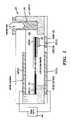
- FIG. 1is a cross sectional, side view of a switch in accordance with one embodiment of the present invention
- FIG. 2Ais a cross sectional, side view of a switch in accordance with another embodiment of the present invention.
- FIG. 2Bis a cross sectional, side view of a switch in accordance with yet another embodiment of the present invention.
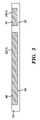
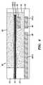
- FIGS. 3 and 5 - 11are cross sectional, side views of steps in a method of making a switch in accordance with another embodiment of the present invention.
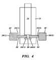
- FIG. 4is a partial, cross sectional, top-view of a step in the method of making the switch.
- FIGS. 12-14are partial, cross sectional, top-view of additional steps in the method of making the switch.
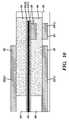
- FIG. 1A switch 10 ( 1 ) in accordance with at least one embodiment of the present invention is illustrated in FIG. 1 .
- the switch 10 ( 1 )includes a switch housing 12 with a chamber 14 , separated portions of a conductive line 16 ( 1 ) and 16 ( 2 ), a beam 18 with imbedded charge and a contactor 20 , and control electrodes 22 ( 1 ) and 22 ( 2 ).
- the present inventionprovides a switch 10 ( 1 ) that utilizes fixed static charge to apply attractive and repulsive forces for activation of the switch and to overcome stiction.
- This switch 10 ( 1 )has lower power requirements to operate, less parasitic capacitance, less mass, and faster switching speed or response than prior designs.
- the switch housing 12defines a chamber 14 in which the switch 10 ( 1 ) is located.
- the switch housing 12is made of several layers of an insulating material, such as silicon dioxide, although other types of materials can be used and the switch housing 12 could comprise a single layer of material in which the chamber 14 is formed.
- the chamber 14has a size which is sufficiently large to hold the components of the switch 10 ( 1 ), although the chamber 14 can have other dimensions.
- control electrodes 22 ( 1 ) and 22 ( 2 ) in the switch housing 12may be separated from each other by a distance of about one micron with each of the control electrodes 22 ( 1 ) and 22 ( 2 ) spaced from the beam 18 by about 0.5 microns, although these dimensions can vary based on the particular application.
- the chamber 14has an access hole 17 used in removing sacrificial material from the chamber 14 although the chamber 14 can have other numbers of access holes.
- a plug 19seals the access hole 17 .
- the chamber 14is vacuum sealed, although it is not required.
- the switch housing 12is vacuum sealed which helps to protect the switch 10 ( 1 ) from contaminates which, for example, might be attracted and adhere to the beam 18 with the imbedded charge.
- each of the separated portions 16 ( 1 ) and 16 ( 2 ) of the conductive line or conductorhas an end 24 ( 1 ) and 24 ( 2 ) which is adjacent to and spaced from the other end 24 ( 1 ) and 24 ( 2 ) in the chamber 14 to form an open circuit along the conductive line.
- the other end 26 ( 1 ) and 26 ( 2 ) of each of the separated portions of the conductive lineextends out from the chamber to form a contact pad.
- the separated portions 16 ( 1 ) and 16 ( 2 ) of the conductive lineare made of a conductive material, such as copper, although another material or materials could be used.
- the beam 18has one end 28 ( 1 ) which is secured to the switch housing 12 and the other end 28 ( 2 ) of the beam 18 extends into the chamber 14 and is spaced from the other side of the chamber 14 , although other configurations for the beam 18 can be used.
- both ends 28 ( 1 ) and 28 ( 2 ) of the beam 18could be secured to the switch housing 12 , although this embodiment would provide less flexibility than having the beam 18 secured at just one end 28 ( 1 ) to the switch housing 12 as shown in FIGS. 1 and 2 .
- the beam 18is made of a material which can hold an imbedded charge.
- the beam 18is made of a composite of silicon oxide and silicon nitride, although the beam 18 could be made of another material or materials.
- the beam 18could be a composite of a plurality of layers of different materials.
- the contactor 20is located at or adjacent one end 28 ( 2 ) of the beam 18 , although the contactor 20 could be located in other locations or could be part of the end 28 ( 1 ) or another section of the beam 18 that was made conductive.
- the contactor 20is positioned on the beam 18 to be in substantial alignment with the ends 24 ( 1 ) and 24 ( 2 ) of the separated portions 16 ( 1 ) and 16 ( 2 ) of the conductive line.
- the contactor 20is made of a conductive material, such as copper, although another material or materials could be used.
- the contactor 20In an open position, the contactor 20 is spaced away from the ends 24 ( 1 ) and 24 ( 2 ) of the separated portions 16 ( 1 ) and 16 ( 2 ) of the conductive line and in a closed position the contractor 20 is located on the ends 24 ( 1 ) and 24 ( 2 ) of each of the separated portions 16 ( 1 ) and 16 ( 2 ) of the conductive line to couple the separated portions 16 ( 1 ) and 16 ( 2 ) of the conductive line together.
- control electrodes 22 ( 1 ) and 22 ( 2 )are located in the chamber 14 of the switch housing 12 and are spaced away from opposing sides of the beam 18 , although other configurations are possible.
- one of the control electrodes 22 ( 1 )could be located outside of the chamber 14 , as shown in the switch 10 ( 2 ) in FIG. 2 or both of the control electrodes 22 ( 1 ) and 22 ( 2 ) could be located outside of the chamber 14 .
- Each of the control electrodes 22 ( 1 ) and 22 ( 2 )is made of a conductive material, such as chrome, although another material or materials could be used.
- a power supply 30is coupled to each of the control electrodes 22 ( 1 ) and 22 ( 2 ) and is used to apply the potential to the control electrodes 22 ( 1 ) and 22 ( 2 ) to open and close the switch 10 ( 1 ).
- the switch 10 ( 1 )is operated by applying a potential across the control electrodes 22 ( 1 ) and 22 ( 2 ).
- a potentialis applied across the control electrodes 22 ( 1 ) and 22 ( 2 )
- the beam 18 with the imbedded chargeis drawn towards one of the control electrodes 22 ( 1 ) or 22 ( 2 ) depending on the polarity of the applied potential.
- This movement of the beam 18 towards one of the control electrodes 22 ( 1 ) or 22 ( 2 )moves the contactor 20 to a closed position resting on ends 24 ( 1 ) and 24 ( 2 ) of each of the separated portions 16 ( 1 ) and 16 ( 2 ) of the conductive line to couple them together.
- the beam 18is repelled away from the control electrode 22 ( 1 ) or 22 ( 2 ) moving the contactor 20 to an open position spaced from the ends 24 ( 1 ) and 24 ( 2 ) of each of the separated portions 16 ( 1 ) and 16 ( 2 ) of the conductive line to open the connection along the conductive line.
- the switch 10 ( 1 )is controlled by electrostatic forces that can be applied to both close and to open the switch 10 ( 1 ). No extraneous current path exists, the energy used to open and close the switch is limited to capacitively coupled displacement current, and the dual force directionality overcomes stiction.
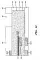
- FIGS. 2A and 2BThe components and operation of the switches 10 ( 2 ) 10 ( 3 ), and 10 ( 4 ) shown in FIGS. 2A and 2B are identical to those for the switch 10 ( 1 ) shown and described with reference FIG. 1 , except as described and illustrated herein. Components in FIGS. 2A and 2B which are identical to components in FIG. 1 have the same reference numeral as those in FIG. 1 .
- control electrode 22 ( 2 )is located outside of the chamber 14 .
- a portion 29 of the switch housing 12separates the control electrode 22 ( 2 ) from the chamber 14 .
- portion 29is made of an insulating material although another material or materials could be used.
- control electrode 22 ( 1 )could be outside of chamber 14 and control electrode 22 ( 2 ) could be inside chamber 14 .
- control electrodes 22 ( 1 ) and 22 ( 2 )are located outside of the chamber 14 .
- Portions 29 and 31 of the switch housing 12separate the control electrodes 22 ( 1 ) and 22 ( 2 ) from the chamber 14 .
- portions 29 and 31 of the switch housing 12are each made of an insulating material, although another material or materials could be used.
- FIGS. 3-14a method for making a switch 10 ( 1 ) in accordance with at least one embodiment will be described.
- three trenches 32 , 34 , and 36are etched into a base material 38 .
- Two of the etched trenches 32 and 34have ends located adjacent and spaced from each other and are used in the forming the separated portions 16 ( 1 ) and 16 ( 2 ) of the conductive line.
- the other trench 36is used to form one of the control electrodes 22 ( 1 ).
- etchingis used in this particular embodiment to form the trenches 32 , 34 , and 36 , other techniques for forming the trenches or opening can also be used.
- a conductive material 40is deposited in the trenches in the base material 38 .
- the conductive material 40 in the two trenches 32 and 34 with the adjacent endsforms the separated portions 16 ( 1 ) and 16 ( 2 ) of the conductive line.
- the conductive material 40 in the other trench 36forms control electrode 22 ( 1 ).
- the conductive material 40 deposited in these trenches 32 , 34 , and 36may also be planarized. Again although in this embodiment, the control electrodes 22 ( 1 ) is formed in the chamber 14 of the switch housing 12 , the control electrode 22 ( 1 ) could be positioned outside of the switch housing 12 .
- an insulating material 42is deposited over the base material 38 and the conductive material 40 in the trenches 32 , 34 , and 36 .
- silicon dioxide, SiO 2is used as the insulating material 42 , although other types of insulating materials can be used.
- the insulating material 42is deposited, the insulating material 42 is etched to extend down to a portion of the conductive material 40 in the trenches 32 , 34 , and 36 .
- a sacrificial material 44is deposited in the etched opening or trench 46 in the insulating material.
- polysiliconis used as the sacrificial material 44 , although another material or materials can be used.
- the sacrificial material 44may be planarized. Although etching is used in this particular embodiment to form opening or trench 46 , other techniques for forming trenches or openings can be used.
- a trench 48is etched into the sacrificial material 44 at a location which is in alignment with a portion of the conductive material 40 in the trenches that form the separated portions 16 ( 1 ) and 16 ( 2 ) of the conductive line.
- a conductive material 50is deposited in the trench 48 in the sacrificial material 44 to form a contactor 20 .
- the conductive material 50may be planarized. Although etching is used in this particular embodiment to form opening or trench 48 , other techniques for forming trenches or openings can be used.
- an insulator 52comprising a pair of insulating layers 53 (1) and 53 (2) are deposited over the insulating material 42 , the sacrificial material 44 , and the conductive material 44 that forms the contactor 20 .
- the insulator 52is patterned to form a cantilever charge holding beam 18 which extends from the insulating layer 42 across a portion of the sacrificial layer 44 and is connected to the contactor 20 .
- the beam 18is patterned, other techniques for forming the beam 18 can be used.
- insulator 52comprises two insulating layers, insulator 52 can be made of more or fewer layers and can be made of another material or materials that can hold fixed charge.
- an insulating material 54is deposited over the insulating material 42 , the beam 18 , and the sacrificial material 44 .
- a trench 56is etched into the insulating material 54 which extends down to a portion of the beam 18 and the sacrificial material 44 .
- a sacrificial material 58is deposited in the trench 56 in the insulating material 54 .
- the sacrificial material 58can be planarized. Sacrificial material 58 can be made of the same or a different material from sacrificial layer 44 and in this embodiment is polysilicon, although another material or materials could be used. Although etching is used in this particular embodiment to form opening or trench 56 , other techniques for forming trenches or openings can be used.
- electronsare injected into the beam 18 from a ballistic energy source 60 to imbed charge in the beam 18 , although other techniques for imbedding the electrons can be used, such as applying an electrical bias to the beam 18 .
- a conductive material 62is deposited over the insulating material 54 and the sacrificial material 58 .
- the conductive material 62is etched to form a control electrode 22 ( 2 ) for the switch 10 ( 1 ).
- the control electrode 22 ( 2 )is formed by patterning, other techniques for forming the control electrode can be used.
- control electrode 22 ( 1 )is formed, an insulating material 64 is deposited over the conductive material, the sacrificial material, and the insulating material.
- the base material 38 and insulating materials 42 , 54 , and 64form the switch housing 12 with the chamber 14 which is filled with the sacrificial materials 44 and 58 , although switch housing 12 could be made from one or other numbers of layers.
- an access hole 66is drilled through the insulating layer 64 to the sacrificial material 58 .
- a single access hole 66is etched, other numbers of access holes can be formed and the hole or holes can be formed through other materials to the sacrificial material 44 and 58 .
- Contact vias to separated portions 16 ( 1 ) and 16 ( 2 ) of the conductive line and control electrodes 22 ( 1 ) and 22 ( 2 )may also be etched or otherwise formed at this time.
- the sacrificial materials 44 and 58removed using xenon difluoride (XeF 2 ) via the access hole 66 , although other techniques for removing sacrificial materials 44 and 58 can be used.
- XeF 2xenon difluoride
- the chamber 14is vacuum sealed when the sacrificial materials 44 and 58 are removed and access hole 66 is sealed with a plug 68 , although the chamber 14 does not have to be vacuum sealed. Once the chamber 14 is sealed, the switch is ready for use.
- the present inventionprovides a switch that utilizes fixed static charge to apply attractive and repulsive forces for activation and is easy to manufacture.
- one method for making a switchis disclosed, other steps in this method and other methods for making the switch can also be used.
- other techniques for imbedding charge in the beamcan be used, such as applying a bias to the beam to imbed charge.
Landscapes
- Micromachines (AREA)
Abstract
Description
Claims (22)
Priority Applications (1)
| Application Number | Priority Date | Filing Date | Title |
|---|---|---|---|
| US10/096,472US7280014B2 (en) | 2001-03-13 | 2002-03-12 | Micro-electro-mechanical switch and a method of using and making thereof |
Applications Claiming Priority (2)
| Application Number | Priority Date | Filing Date | Title |
|---|---|---|---|
| US27538601P | 2001-03-13 | 2001-03-13 | |
| US10/096,472US7280014B2 (en) | 2001-03-13 | 2002-03-12 | Micro-electro-mechanical switch and a method of using and making thereof |
Publications (2)
| Publication Number | Publication Date |
|---|---|
| US20020131228A1 US20020131228A1 (en) | 2002-09-19 |
| US7280014B2true US7280014B2 (en) | 2007-10-09 |
Family
ID=23052073
Family Applications (1)
| Application Number | Title | Priority Date | Filing Date |
|---|---|---|---|
| US10/096,472Expired - LifetimeUS7280014B2 (en) | 2001-03-13 | 2002-03-12 | Micro-electro-mechanical switch and a method of using and making thereof |
Country Status (2)
| Country | Link |
|---|---|
| US (1) | US7280014B2 (en) |
| WO (1) | WO2002073673A1 (en) |
Cited By (22)
| Publication number | Priority date | Publication date | Assignee | Title |
|---|---|---|---|---|
| US20050162244A1 (en)* | 2002-07-26 | 2005-07-28 | Yasuyuki Naito | Switch |
| US20070046214A1 (en)* | 2005-08-26 | 2007-03-01 | Pasch Nicholas F | Apparatus comprising an array of switches and display |
| US20070236307A1 (en)* | 2006-04-10 | 2007-10-11 | Lianjun Liu | Methods and apparatus for a packaged MEMS switch |
| US20070256918A1 (en)* | 2004-03-31 | 2007-11-08 | Chou Tsung-Kuan A | Collapsible contact switch |
| US20080060919A1 (en)* | 2005-01-21 | 2008-03-13 | Matsushita Electric Industrial Co., Ltd. | Electro-Mechanical Switch |
| US7378775B2 (en) | 2001-10-26 | 2008-05-27 | Nth Tech Corporation | Motion based, electrostatic power source and methods thereof |
| US7408236B2 (en) | 2003-08-29 | 2008-08-05 | Nth Tech | Method for non-damaging charge injection and system thereof |
| US20080283373A1 (en)* | 2004-06-14 | 2008-11-20 | Stmicroelectronics S.A. | Assembly of a Microswitch and of an Acoustic Resonator |
| US20090026880A1 (en)* | 2007-07-26 | 2009-01-29 | Lianjun Liu | Micromechanical device with piezoelectric and electrostatic actuation and method therefor |
| US20090071807A1 (en)* | 2007-08-08 | 2009-03-19 | Kabushiki Kaisha Toshiba | Mems switch and method of fabricating the same |
| US20100163376A1 (en)* | 2007-06-22 | 2010-07-01 | Korea Advanced Institute Of Science And Technology | Electrostatic Actuator |
| US20110063713A1 (en)* | 2009-09-17 | 2011-03-17 | Qualcomm Mems Technologies, Inc. | Anti-stiction electrode |
| US20120169179A1 (en)* | 2008-12-08 | 2012-07-05 | Omron Corporation | Energy conversion device of electrostatic induction type |
| US20120175715A1 (en)* | 2011-01-11 | 2012-07-12 | Rf Micro Devices, Inc. | Encapsulated micro-electromechanical system switch and method of manufacturing the same |
| US20130192964A1 (en)* | 2008-04-22 | 2013-08-01 | International Business Machines Corporation | Mems switches with reduced switching voltage and methods of manufacture |
| US8581308B2 (en) | 2004-02-19 | 2013-11-12 | Rochester Institute Of Technology | High temperature embedded charge devices and methods thereof |
| US9446940B2 (en) | 2014-10-03 | 2016-09-20 | Freescale Semiconductor, Inc. | Stress isolation for MEMS device |
| US9458008B1 (en)* | 2015-03-16 | 2016-10-04 | Freescale Semiconductor, Inc. | Method of making a MEMS die having a MEMS device on a suspended structure |
| US9828241B2 (en)* | 2015-12-11 | 2017-11-28 | Hyundai Motor Company | Manufacturing method of micro-electro-mechanical system sensor capable of preventing diffusion phenomenon and reflow phenomenon |
| US9837526B2 (en) | 2014-12-08 | 2017-12-05 | Nxp Usa, Inc. | Semiconductor device wtih an interconnecting semiconductor electrode between first and second semiconductor electrodes and method of manufacture therefor |
| US10348295B2 (en) | 2015-11-19 | 2019-07-09 | Nxp Usa, Inc. | Packaged unidirectional power transistor and control circuit therefore |
| US20210356336A1 (en)* | 2020-05-14 | 2021-11-18 | Commissariat A L'energie Atomique Et Aux Energies Alternatives | Detection device using piezoresistive transduction |
Families Citing this family (42)
| Publication number | Priority date | Publication date | Assignee | Title |
|---|---|---|---|---|
| US6872984B1 (en) | 1998-07-29 | 2005-03-29 | Silicon Light Machines Corporation | Method of sealing a hermetic lid to a semiconductor die at an angle |
| US6303986B1 (en) | 1998-07-29 | 2001-10-16 | Silicon Light Machines | Method of and apparatus for sealing an hermetic lid to a semiconductor die |
| US6956878B1 (en) | 2000-02-07 | 2005-10-18 | Silicon Light Machines Corporation | Method and apparatus for reducing laser speckle using polarization averaging |
| WO2002097865A2 (en) | 2001-05-31 | 2002-12-05 | Rochester Institute Of Technology | Fluidic valves, agitators, and pumps and methods thereof |
| US6865346B1 (en) | 2001-06-05 | 2005-03-08 | Silicon Light Machines Corporation | Fiber optic transceiver |
| US6747781B2 (en) | 2001-06-25 | 2004-06-08 | Silicon Light Machines, Inc. | Method, apparatus, and diffuser for reducing laser speckle |
| US6829092B2 (en)* | 2001-08-15 | 2004-12-07 | Silicon Light Machines, Inc. | Blazed grating light valve |
| US6930364B2 (en) | 2001-09-13 | 2005-08-16 | Silicon Light Machines Corporation | Microelectronic mechanical system and methods |
| US7211923B2 (en) | 2001-10-26 | 2007-05-01 | Nth Tech Corporation | Rotational motion based, electrostatic power source and methods thereof |
| US20040031912A1 (en)* | 2001-10-31 | 2004-02-19 | Wong Marvin Glenn | Method of eliminating brownian noise in micromachined varactors |
| DE60229675D1 (en)* | 2001-11-09 | 2008-12-11 | Wispry Inc | Three-layer beam MEMS device and related methods |
| US6800238B1 (en) | 2002-01-15 | 2004-10-05 | Silicon Light Machines, Inc. | Method for domain patterning in low coercive field ferroelectrics |
| US6839479B2 (en) | 2002-05-29 | 2005-01-04 | Silicon Light Machines Corporation | Optical switch |
| US7054515B1 (en) | 2002-05-30 | 2006-05-30 | Silicon Light Machines Corporation | Diffractive light modulator-based dynamic equalizer with integrated spectral monitor |
| US6822797B1 (en) | 2002-05-31 | 2004-11-23 | Silicon Light Machines, Inc. | Light modulator structure for producing high-contrast operation using zero-order light |
| WO2003106326A2 (en)* | 2002-06-13 | 2003-12-24 | Coventor, Incorporated | Micro-electro-mechanical system (mems) variable capacitor apparatuses and related methods |
| US6829258B1 (en) | 2002-06-26 | 2004-12-07 | Silicon Light Machines, Inc. | Rapidly tunable external cavity laser |
| US6813059B2 (en) | 2002-06-28 | 2004-11-02 | Silicon Light Machines, Inc. | Reduced formation of asperities in contact micro-structures |
| US6908201B2 (en) | 2002-06-28 | 2005-06-21 | Silicon Light Machines Corporation | Micro-support structures |
| US7057795B2 (en) | 2002-08-20 | 2006-06-06 | Silicon Light Machines Corporation | Micro-structures with individually addressable ribbon pairs |
| US6928207B1 (en) | 2002-12-12 | 2005-08-09 | Silicon Light Machines Corporation | Apparatus for selectively blocking WDM channels |
| US6987600B1 (en) | 2002-12-17 | 2006-01-17 | Silicon Light Machines Corporation | Arbitrary phase profile for better equalization in dynamic gain equalizer |
| US7057819B1 (en) | 2002-12-17 | 2006-06-06 | Silicon Light Machines Corporation | High contrast tilting ribbon blazed grating |
| US6934070B1 (en) | 2002-12-18 | 2005-08-23 | Silicon Light Machines Corporation | Chirped optical MEM device |
| US6927891B1 (en) | 2002-12-23 | 2005-08-09 | Silicon Light Machines Corporation | Tilt-able grating plane for improved crosstalk in 1×N blaze switches |
| KR100506283B1 (en)* | 2003-01-14 | 2005-08-05 | 삼성전자주식회사 | Ear-microphone connection apparatus by using a interface connector of portable phone |
| US7068372B1 (en) | 2003-01-28 | 2006-06-27 | Silicon Light Machines Corporation | MEMS interferometer-based reconfigurable optical add-and-drop multiplexor |
| US6947613B1 (en) | 2003-02-11 | 2005-09-20 | Silicon Light Machines Corporation | Wavelength selective switch and equalizer |
| US6922272B1 (en) | 2003-02-14 | 2005-07-26 | Silicon Light Machines Corporation | Method and apparatus for leveling thermal stress variations in multi-layer MEMS devices |
| US6922273B1 (en) | 2003-02-28 | 2005-07-26 | Silicon Light Machines Corporation | PDL mitigation structure for diffractive MEMS and gratings |
| US7027202B1 (en) | 2003-02-28 | 2006-04-11 | Silicon Light Machines Corp | Silicon substrate as a light modulator sacrificial layer |
| US6967718B1 (en) | 2003-02-28 | 2005-11-22 | Silicon Light Machines Corportion | Method and apparatus for monitoring WDM channels and for analyzing dispersed spectrum of light |
| US7391973B1 (en) | 2003-02-28 | 2008-06-24 | Silicon Light Machines Corporation | Two-stage gain equalizer |
| US7042611B1 (en) | 2003-03-03 | 2006-05-09 | Silicon Light Machines Corporation | Pre-deflected bias ribbons |
| JP4333417B2 (en)* | 2003-04-02 | 2009-09-16 | ソニー株式会社 | Micromachine manufacturing method |
| US7287328B2 (en) | 2003-08-29 | 2007-10-30 | Rochester Institute Of Technology | Methods for distributed electrode injection |
| DE102004010150B9 (en) | 2004-02-27 | 2012-01-26 | Eads Deutschland Gmbh | High-frequency MEMS switch with bent switching element and method for its production |
| CN101438366B (en)* | 2006-03-08 | 2011-10-26 | 维斯普瑞公司 | Microelectromechanical systems (MEMS) variable capacitors, actuation components, and related methods |
| JP5127210B2 (en)* | 2006-11-30 | 2013-01-23 | 株式会社日立製作所 | Semiconductor device in which MEMS sensor is embedded |
| US7692519B2 (en) | 2007-12-21 | 2010-04-06 | General Electric Company | MEMS switch with improved standoff voltage control |
| US20110168378A1 (en)* | 2010-01-14 | 2011-07-14 | Irvine Sensors Corporation | Thermal power distribution system |
| CN111446089B (en)* | 2020-03-12 | 2022-04-26 | 上海集成电路研发中心有限公司 | MEMS switch structure and manufacturing method |
Citations (208)
| Publication number | Priority date | Publication date | Assignee | Title |
|---|---|---|---|---|
| US2567373A (en) | 1949-06-10 | 1951-09-11 | Rca Corp | Electrostatic generator |
| US2588513A (en) | 1949-06-10 | 1952-03-11 | Rca Corp | Electrostatic high-voltage generator |
| US2978066A (en) | 1959-05-07 | 1961-04-04 | Honeywell Regulator Co | Gas cleaning apparatus |
| US3118022A (en) | 1961-08-07 | 1964-01-14 | Bell Telephone Labor Inc | Electroacoustic transducer |
| US3397278A (en) | 1965-05-06 | 1968-08-13 | Mallory & Co Inc P R | Anodic bonding |
| US3405334A (en) | 1967-03-06 | 1968-10-08 | Homer H. Jewett | Electrostatic power generator driven by pneumatic power means |
| US3487610A (en) | 1965-03-26 | 1970-01-06 | Du Pont | Electrostatic filter unit with high stable charge and its manufacture |
| US3715500A (en) | 1971-07-21 | 1973-02-06 | Bell Telephone Labor Inc | Unidirectional microphones |
| US3731163A (en) | 1972-03-22 | 1973-05-01 | United Aircraft Corp | Low voltage charge storage memory element |
| US3742767A (en) | 1971-02-02 | 1973-07-03 | Onera (Off Nat Aerospatiale) | Ball electrostatic accelerometer |
| US3786495A (en) | 1972-05-17 | 1974-01-15 | Ncr | Stored charge transducer |
| US3858307A (en) | 1969-12-11 | 1975-01-07 | Matsushita Electric Industrial Co Ltd | Electrostatic transducer |
| US3924324A (en) | 1973-07-05 | 1975-12-09 | Sony Corp | Method of making electret |
| US4047214A (en) | 1975-09-04 | 1977-09-06 | Westinghouse Electric Corporation | Electrostatically bonded dielectric-on-semiconductor device, and a method of making the same |
| US4102202A (en) | 1976-11-26 | 1978-07-25 | The Singer Company | Electrostatic accelerometer |
| US4115914A (en) | 1976-03-26 | 1978-09-26 | Hughes Aircraft Company | Electrically erasable non-volatile semiconductor memory |
| US4126822A (en) | 1977-05-27 | 1978-11-21 | Wahlstrom Sven E | Electrostatic generator and motor |
| US4160882A (en) | 1978-03-13 | 1979-07-10 | Driver Michael L | Double diaphragm electrostatic transducer each diaphragm comprising two plastic sheets having different charge carrying characteristics |
| US4166729A (en) | 1977-07-26 | 1979-09-04 | The United States Of America As Represented By The Secretary Of The Navy | Collector plates for electrostatic precipitators |
| US4285714A (en) | 1978-12-07 | 1981-08-25 | Spire Corporation | Electrostatic bonding using externally applied pressure |
| US4288735A (en) | 1979-09-17 | 1981-09-08 | Mcdonnell Douglas Corp. | Vibrating electret reed voltage generator |
| US4340953A (en) | 1979-05-14 | 1982-07-20 | Nippon Hoso Kyokai | Information recording medium and recording and reproducing system using the same |
| JPS5829379A (en) | 1981-08-13 | 1983-02-21 | Toko Seiki Seisakusho:Kk | Electrostatic generator |
| US4375718A (en) | 1981-03-12 | 1983-03-08 | Surgikos, Inc. | Method of making fibrous electrets |
| US4490772A (en) | 1983-06-13 | 1984-12-25 | Blickstein Martin J | Voltage and mechanically variable trimmer capacitor |
| US4504550A (en) | 1982-07-21 | 1985-03-12 | James Frederick John Johnson | Releasably mutually-adherent materials |
| US4513049A (en) | 1983-04-26 | 1985-04-23 | Mitsui Petrochemical Industries, Ltd. | Electret article |
| US4581624A (en) | 1984-03-01 | 1986-04-08 | Allied Corporation | Microminiature semiconductor valve |
| US4585209A (en) | 1983-10-27 | 1986-04-29 | Harry E. Aine | Miniature valve and method of making same |
| US4626729A (en) | 1984-05-04 | 1986-12-02 | Jacques Lewiner | Electroacoustic piezoelectric transducers |
| US4626263A (en) | 1984-04-24 | 1986-12-02 | Mitsui Petrochemical Industries, Ltd. | High-performance electret and air filter |
| US4701640A (en) | 1985-03-11 | 1987-10-20 | Telex Communications, Inc. | Electret transducer and method of fabrication |
| JPS62297534A (en) | 1986-06-17 | 1987-12-24 | Seiko Epson Corp | electric field bearing |
| US4716331A (en) | 1985-12-30 | 1987-12-29 | Motorola Inc. | Electrically variable piezoelectric hybrid capacitor |
| US4736629A (en) | 1985-12-20 | 1988-04-12 | Silicon Designs, Inc. | Micro-miniature accelerometer |
| US4789803A (en) | 1987-08-04 | 1988-12-06 | Sarcos, Inc. | Micropositioner systems and methods |
| US4789504A (en) | 1984-03-19 | 1988-12-06 | Toyo Boseki Kabushiki Kaisha | Electretized material for a dust filter |
| US4794370A (en) | 1984-08-21 | 1988-12-27 | Bos-Knox Ltd. | Peristaltic electrostatic binary device |
| US4874659A (en) | 1984-10-24 | 1989-10-17 | Toray Industries | Electret fiber sheet and method of producing same |
| US4905701A (en) | 1988-06-15 | 1990-03-06 | National Research Development Corporation | Apparatus and method for detecting small changes in attached mass of piezoelectric devices used as sensors |
| US4922756A (en) | 1988-06-20 | 1990-05-08 | Triton Technologies, Inc. | Micro-machined accelerometer |
| US4945068A (en) | 1988-10-25 | 1990-07-31 | Matsushita Electronics Corporation | Manufacturing method of semiconductor nonvolatile memory device |
| US4944854A (en) | 1983-11-08 | 1990-07-31 | Celanese Corporation | Electret process and products |
| JPH02219478A (en) | 1989-02-17 | 1990-09-03 | Seiko Epson Corp | electret generator |
| US4958317A (en) | 1987-07-27 | 1990-09-18 | Mitsubishi Denki Kabushiki Kaisha | Nonvolatile semiconductor memory device and a writing method using electron tunneling |
| US4965244A (en) | 1988-09-19 | 1990-10-23 | Regents Of The University Of Minnesota | CaF2 passivation layers for high temperature superconductors |
| US4996627A (en) | 1989-01-30 | 1991-02-26 | Dresser Industries, Inc. | High sensitivity miniature pressure transducer |
| US4997521A (en) | 1987-05-20 | 1991-03-05 | Massachusetts Institute Of Technology | Electrostatic micromotor |
| US5020030A (en) | 1988-10-31 | 1991-05-28 | Huber Robert J | Nonvolatile SNOS memory cell with induced capacitor |
| US5050435A (en) | 1989-07-18 | 1991-09-24 | The Boeing Company | Position detection system for a suspended particle accelerometer |
| US5054081A (en) | 1985-04-02 | 1991-10-01 | West Roger A | Electrostatic transducer with improved bass response utilizing disturbed bass resonance energy |
| US5057710A (en) | 1988-05-13 | 1991-10-15 | Toray Industries, Inc. | Electret materials and the method for preparing the electret materials |
| US5081513A (en) | 1991-02-28 | 1992-01-14 | Xerox Corporation | Electronic device with recovery layer proximate to active layer |
| US5082242A (en) | 1989-12-27 | 1992-01-21 | Ulrich Bonne | Electronic microvalve apparatus and fabrication |
| US5088326A (en) | 1989-05-24 | 1992-02-18 | Mitsubishi Denki K.K. | Piezoelectric accelerometer for automobiles |
| US5092174A (en) | 1989-10-19 | 1992-03-03 | Texas Instruments Incorporated | Capacitance accelerometer |
| US5096388A (en) | 1990-03-22 | 1992-03-17 | The Charles Stark Draper Laboratory, Inc. | Microfabricated pump |
| US5095752A (en) | 1988-11-15 | 1992-03-17 | Hitachi, Ltd. | Capacitance type accelerometer |
| US5108470A (en) | 1988-11-01 | 1992-04-28 | William Pick | Charging element having odor and gas absorbing properties for an electrostatic air filter |
| US5112677A (en) | 1987-11-28 | 1992-05-12 | Toyo Boseki Kabushiki Kaisha | Electret sheet and a method for the production of the same |
| US5118942A (en) | 1990-02-05 | 1992-06-02 | Hamade Thomas A | Electrostatic charging apparatus and method |
| US5129794A (en) | 1990-10-30 | 1992-07-14 | Hewlett-Packard Company | Pump apparatus |
| US5132934A (en) | 1989-06-23 | 1992-07-21 | The Board Of Trustees Of The Leland Stanford Junior University | Method and apparatus for storing digital information in the form of stored charges |
| JPH04236172A (en) | 1991-01-18 | 1992-08-25 | Masafumi Yano | Space holding device using electrostatic force or magnetic force |
| US5143854A (en) | 1989-06-07 | 1992-09-01 | Affymax Technologies N.V. | Large scale photolithographic solid phase synthesis of polypeptides and receptor binding screening thereof |
| US5156810A (en) | 1989-06-15 | 1992-10-20 | Biocircuits Corporation | Biosensors employing electrical, optical and mechanical signals |
| US5164319A (en) | 1985-08-22 | 1992-11-17 | Molecular Devices Corporation | Multiple chemically modulated capacitance determination |
| US5180623A (en) | 1989-12-27 | 1993-01-19 | Honeywell Inc. | Electronic microvalve apparatus and fabrication |
| US5189641A (en) | 1987-06-08 | 1993-02-23 | Fujitsu Limited | Non-volatile random access memory device |
| US5207103A (en) | 1987-06-01 | 1993-05-04 | Wise Kensall D | Ultraminiature single-crystal sensor with movable member |
| US5228373A (en) | 1990-01-08 | 1993-07-20 | Robert A. Foisie | Method and apparatus using electrostatic charges to temporarily hold packets of paper |
| US5231045A (en) | 1988-12-08 | 1993-07-27 | Fujitsu Limited | Method of producing semiconductor-on-insulator structure by besol process with charged insulating layers |
| US5238223A (en) | 1989-08-11 | 1993-08-24 | Robert Bosch Gmbh | Method of making a microvalve |
| US5256176A (en) | 1990-03-12 | 1993-10-26 | Mitsui Petrochemical Industries, Ltd. | Film electret and an electret filter |
| US5284179A (en) | 1991-05-30 | 1994-02-08 | Hitachi, Ltd. | Valve and semiconductor fabricating equipment using the same |
| US5284692A (en) | 1991-10-24 | 1994-02-08 | Bell Dennis J | Electrostatic evacuated insulating sheet |
| US5323999A (en) | 1991-08-08 | 1994-06-28 | Honeywell Inc. | Microstructure gas valve control |
| US5334238A (en) | 1990-11-27 | 1994-08-02 | United Technologies Corporation | Cleaner method for electrostatic precipitator |
| US5336904A (en) | 1991-05-10 | 1994-08-09 | Mitsubishi Denki Kabushiki Kaisha | Field effect element utilizing resonant-tunneling and a method of manufacturing the same |
| US5336062A (en) | 1990-02-27 | 1994-08-09 | Fraunhofer-Gesellschaft Zur Forderung Der Angewandten Forschung E.V. | Microminiaturized pump |
| US5349492A (en) | 1991-12-26 | 1994-09-20 | Yamatake-Honeywell Co., Ltd. | Capacitive pressure sensor |
| US5348571A (en) | 1992-01-09 | 1994-09-20 | Metallgesellschaft Aktiengesellschaft | Apparatus for dedusting a gas at high temperature |
| US5355577A (en) | 1992-06-23 | 1994-10-18 | Cohn Michael B | Method and apparatus for the assembly of microfabricated devices |
| US5365790A (en) | 1992-04-02 | 1994-11-22 | Motorola, Inc. | Device with bonded conductive and insulating substrates and method therefore |
| US5367429A (en) | 1991-10-18 | 1994-11-22 | Hitachi, Ltd | Electrostatic type micro transducer and control system using the same |
| US5392650A (en) | 1991-01-11 | 1995-02-28 | Northrop Grumman Corporation | Micromachined accelerometer gyroscope |
| US5417312A (en) | 1990-05-30 | 1995-05-23 | Hitachi, Ltd. | Semiconductor acceleration sensor and vehicle control system using the same |
| US5417235A (en) | 1993-07-28 | 1995-05-23 | Regents Of The University Of Michigan | Integrated microvalve structures with monolithic microflow controller |
| US5419953A (en) | 1993-05-20 | 1995-05-30 | Chapman; Rick L. | Multilayer composite air filtration media |
| US5441597A (en) | 1992-12-01 | 1995-08-15 | Honeywell Inc. | Microstructure gas valve control forming method |
| US5445008A (en) | 1994-03-24 | 1995-08-29 | Martin Marietta Energy Systems, Inc. | Microbar sensor |
| US5474599A (en) | 1992-08-11 | 1995-12-12 | United Air Specialists, Inc. | Apparatus for electrostatically cleaning particulates from air |
| US5488864A (en) | 1994-12-19 | 1996-02-06 | Ford Motor Company | Torsion beam accelerometer with slotted tilt plate |
| US5491604A (en) | 1992-12-11 | 1996-02-13 | The Regents Of The University Of California | Q-controlled microresonators and tunable electronic filters using such resonators |
| US5496507A (en) | 1993-08-17 | 1996-03-05 | Minnesota Mining And Manufacturing Company | Method of charging electret filter media |
| US5512882A (en) | 1991-08-07 | 1996-04-30 | Transducer Research, Inc. | Chemical sensing apparatus and methods |
| US5519240A (en) | 1993-02-26 | 1996-05-21 | Nec Corporation | Microshutter horizontally movable by electrostatic repulsion |
| US5520522A (en) | 1993-10-01 | 1996-05-28 | Tdk Corporation | Valve arrangement for a micro pump |
| US5526172A (en) | 1993-07-27 | 1996-06-11 | Texas Instruments Incorporated | Microminiature, monolithic, variable electrical signal processor and apparatus including same |
| US5567336A (en) | 1994-10-24 | 1996-10-22 | Matsushita Electric Industrial Co., Ltd. | Laser ablation forward metal deposition with electrostatic assisted bonding |
| JPH08308258A (en) | 1995-05-10 | 1996-11-22 | Kansai Electric Power Co Inc:The | Running water generator |
| US5591679A (en) | 1995-04-12 | 1997-01-07 | Sensonor A/S | Sealed cavity arrangement method |
| US5593479A (en) | 1995-02-02 | 1997-01-14 | Hmi Industries, Inc. | Filter system |
| US5593476A (en) | 1994-06-09 | 1997-01-14 | Coppom Technologies | Method and apparatus for use in electronically enhanced air filtration |
| US5616844A (en) | 1993-12-27 | 1997-04-01 | Hitachi, Ltd. | Capacitance type acceleration sensor |
| US5635739A (en) | 1990-02-14 | 1997-06-03 | The Charles Stark Draper Laboratory, Inc. | Micromechanical angular accelerometer with auxiliary linear accelerometer |
| US5640133A (en) | 1995-06-23 | 1997-06-17 | Cornell Research Foundation, Inc. | Capacitance based tunable micromechanical resonators |
| US5668303A (en) | 1992-04-30 | 1997-09-16 | Forschung E.V Fraunhofer-Gesellschaft Zur Foerderung Der Angewandten | Sensor having a membrane as part of an electromechanical resonance circuit forming receiver and transmitter converter with interdigital structures spaced apart from one another |
| US5671905A (en) | 1995-06-21 | 1997-09-30 | Hopkins, Jr.; Dean A. | Electrochemical actuator and method of making same |
| US5677617A (en) | 1994-09-16 | 1997-10-14 | Kabushiki Kaisha Toshiba | Micro power supply device using switching element |
| US5698771A (en) | 1995-03-30 | 1997-12-16 | The United States Of America As Represented By The United States National Aeronautics And Space Administration | Varying potential silicon carbide gas sensor |
| US5739834A (en) | 1989-11-29 | 1998-04-14 | Dai Nippon Printing Co., Ltd. | Electrostatic charge information reproducing method |
| US5747692A (en) | 1991-01-28 | 1998-05-05 | Sarcos Group | Sensor system for determining acceleration |
| US5771148A (en) | 1995-11-17 | 1998-06-23 | Motorola, Inc. | Intercalation-based voltage variable capacitor |
| US5777977A (en) | 1995-08-23 | 1998-07-07 | Sony Corporation | Recording and reproducing apparatus |
| US5788468A (en) | 1994-11-03 | 1998-08-04 | Memstek Products, Llc | Microfabricated fluidic devices |
| US5793485A (en) | 1995-03-20 | 1998-08-11 | Sandia Corporation | Resonant-cavity apparatus for cytometry or particle analysis |
| US5798146A (en) | 1995-09-14 | 1998-08-25 | Tri-Star Technologies | Surface charging to improve wettability |
| US5807425A (en) | 1993-07-17 | 1998-09-15 | Gibbs; Robert William | Electrofilter |
| US5812163A (en) | 1996-02-13 | 1998-09-22 | Hewlett-Packard Company | Ink jet printer firing assembly with flexible film expeller |
| US5839062A (en) | 1994-03-18 | 1998-11-17 | The Regents Of The University Of California | Mixing, modulation and demodulation via electromechanical resonators |
| US5846708A (en) | 1991-11-19 | 1998-12-08 | Massachusetts Institiute Of Technology | Optical and electrical methods and apparatus for molecule detection |
| US5846302A (en) | 1997-04-24 | 1998-12-08 | Aqua-Air Technologies, Inc. | Electrostatic air filter device |
| US5871567A (en) | 1996-12-12 | 1999-02-16 | Dana Corporation | Dual Media air filter with electrostatic charge |
| US5897097A (en) | 1996-09-06 | 1999-04-27 | Xerox Corporation | Passively addressable fluid valves having S-shaped blocking films |
| US5908603A (en) | 1997-07-03 | 1999-06-01 | Industrial Technology Research Institute | Ozone generator having micro pump |
| US5914553A (en) | 1997-06-16 | 1999-06-22 | Cornell Research Foundation, Inc. | Multistable tunable micromechanical resonators |
| US5919364A (en) | 1996-06-24 | 1999-07-06 | Regents Of The University Of California | Microfabricated filter and shell constructed with a permeable membrane |
| US5920011A (en) | 1991-02-08 | 1999-07-06 | Alliedsignal Inc. | Micromachined rate and acceleration sensor |
| US5941501A (en) | 1996-09-06 | 1999-08-24 | Xerox Corporation | Passively addressable cantilever valves |
| US5959516A (en) | 1998-01-08 | 1999-09-28 | Rockwell Science Center, Llc | Tunable-trimmable micro electro mechanical system (MEMS) capacitor |
| US5969250A (en) | 1990-10-17 | 1999-10-19 | The Charles Stark Draper Laboratory, Inc. | Micromechanical accelerometer having a peripherally suspended proof mass |
| US5967163A (en) | 1996-01-30 | 1999-10-19 | Abbott Laboratories | Actuator and method |
| US5971355A (en) | 1996-11-27 | 1999-10-26 | Xerox Corporation | Microdevice valve structures to fluid control |
| US5993520A (en) | 1998-01-16 | 1999-11-30 | Yu; Chi-Chin | Electronic dust collecting type air purifier |
| US5994982A (en) | 1997-07-18 | 1999-11-30 | Trw Inc. | MEMS switched resonators for VCO applications |
| US6007309A (en) | 1995-12-13 | 1999-12-28 | Hartley; Frank T. | Micromachined peristaltic pumps |
| US6032923A (en) | 1998-01-08 | 2000-03-07 | Xerox Corporation | Fluid valves having cantilevered blocking films |
| US6033852A (en) | 1996-09-27 | 2000-03-07 | University Of Maine | Monolithic piezoelectric sensor (MPS) for sensing chemical, biochemical and physical measurands |
| US6037797A (en) | 1997-07-11 | 2000-03-14 | Semiconductor Diagnostics, Inc. | Measurement of the interface trap charge in an oxide semiconductor layer interface |
| US6048692A (en) | 1997-10-07 | 2000-04-11 | Motorola, Inc. | Sensors for electrically sensing binding events for supported molecular receptors |
| US6051853A (en) | 1996-10-03 | 2000-04-18 | Hitachi, Ltd. | Semiconductor pressure sensor including reference capacitor on the same substrate |
| US6089534A (en) | 1998-01-08 | 2000-07-18 | Xerox Corporation | Fast variable flow microelectromechanical valves |
| US6094102A (en) | 1999-04-30 | 2000-07-25 | Rockwell Science Center, Llc | Frequency synthesizer using micro electro mechanical systems (MEMS) technology and method |
| US6106245A (en) | 1997-10-09 | 2000-08-22 | Honeywell | Low cost, high pumping rate electrostatically actuated mesopump |
| US6124632A (en) | 1999-07-23 | 2000-09-26 | Industrial Technology Research Institute | Monolithic silicon mass flow control structure |
| US6123316A (en) | 1996-11-27 | 2000-09-26 | Xerox Corporation | Conduit system for a valve array |
| US6126140A (en) | 1997-12-29 | 2000-10-03 | Honeywell International Inc. | Monolithic bi-directional microvalve with enclosed drive electric field |
| US6127812A (en) | 1999-02-16 | 2000-10-03 | General Electric Company | Integrated environmental energy extractor |
| JP2000304567A (en) | 1999-04-16 | 2000-11-02 | Matsushita Electric Ind Co Ltd | Displacement sensor |
| US6149190A (en) | 1993-05-26 | 2000-11-21 | Kionix, Inc. | Micromechanical accelerometer for automotive applications |
| US6168395B1 (en) | 1996-02-10 | 2001-01-02 | Fraunhofer-Gesellschaft Zur Foerderung Der Angewandten Forschung E.V. | Bistable microactuator with coupled membranes |
| US6168948B1 (en) | 1995-06-29 | 2001-01-02 | Affymetrix, Inc. | Miniaturized genetic analysis systems and methods |
| US6170332B1 (en) | 1993-05-26 | 2001-01-09 | Cornell Research Foundation, Inc. | Micromechanical accelerometer for automotive applications |
| US6177351B1 (en) | 1997-12-24 | 2001-01-23 | Texas Instruments Incorporated | Method and structure for etching a thin film perovskite layer |
| US6181009B1 (en) | 1994-07-12 | 2001-01-30 | Mitsubishi Denki Kabushiki Kaisha | Electronic component with a lead frame and insulating coating |
| US6197139B1 (en) | 1998-01-09 | 2001-03-06 | Korea Institute Of Science & Tech. | Method for electrostatic thermal bonding of a pair of glass substrates by utilizing a silicon thin film |
| US6204737B1 (en) | 1998-06-02 | 2001-03-20 | Nokia Mobile Phones, Ltd | Piezoelectric resonator structures with a bending element performing a voltage controlled switching function |
| US6214094B1 (en) | 1997-10-01 | 2001-04-10 | 3M Innovative Properties Company | Electret filters that exhibit increased oily mist resistance |
| US6238946B1 (en) | 1999-08-17 | 2001-05-29 | International Business Machines Corporation | Process for fabricating single crystal resonant devices that are compatible with integrated circuit processing |
| US6255758B1 (en) | 1998-12-29 | 2001-07-03 | Honeywell International Inc. | Polymer microactuator array with macroscopic force and displacement |
| US6265758B1 (en) | 1992-05-19 | 2001-07-24 | Sel Corporation | Semiconductor active electrostatic device |
| US6275122B1 (en) | 1999-08-17 | 2001-08-14 | International Business Machines Corporation | Encapsulated MEMS band-pass filter for integrated circuits |
| US6287776B1 (en) | 1998-02-02 | 2001-09-11 | Signature Bioscience, Inc. | Method for detecting and classifying nucleic acid hybridization |
| US6324914B1 (en) | 1997-03-20 | 2001-12-04 | Alliedsignal, Inc. | Pressure sensor support base with cavity |
| US20010047689A1 (en) | 1998-03-10 | 2001-12-06 | Mcintosh Robert B. | Method to force-balance capacitive transducers |
| US20020000649A1 (en)* | 1998-04-17 | 2002-01-03 | Tilmans Hendrikus A.C. | Method of fabrication of a microstructure having an internal cavity |
| US6336353B2 (en) | 1997-10-08 | 2002-01-08 | Symyx Technologies, Inc. | Method and apparatus for characterizing materials by using a mechanical resonator |
| US20020012937A1 (en) | 2000-06-23 | 2002-01-31 | Tender Leonard M. | Microelectronic device and method for label-free detection and quantification of biological and chemical molecules |
| US6384353B1 (en)* | 2000-02-01 | 2002-05-07 | Motorola, Inc. | Micro-electromechanical system device |
| US6395638B1 (en) | 1997-05-12 | 2002-05-28 | Fraunhofer-Gesellschaft Zur Forderung Der Angewandten Forschung E.V. | Method for producing a micromembrane pump body |
| US20020072201A1 (en) | 2000-12-13 | 2002-06-13 | Rochester Institute Of Technology | Method for electrostatic force bonding and a system thereof |
| US6423148B1 (en) | 1998-09-07 | 2002-07-23 | Nec Corporation | Substrate-cleaning method and substrate-cleaning solution |
| US6431212B1 (en) | 2000-05-24 | 2002-08-13 | Jon W. Hayenga | Valve for use in microfluidic structures |
| US20020131230A1 (en) | 2001-03-13 | 2002-09-19 | Potter Michael D. | Micro-electro-mechanical varactor and a method of making and using thereof |
| US6469785B1 (en) | 1996-08-16 | 2002-10-22 | Zeptosens Ag | Optical detection device based on semi-conductor laser array |
| US6470754B1 (en) | 1998-08-19 | 2002-10-29 | Wisconsin Alumni Research Foundation | Sealed capacitive pressure sensors |
| US6485273B1 (en) | 2000-09-01 | 2002-11-26 | Mcnc | Distributed MEMS electrostatic pumping devices |
| US20020182091A1 (en) | 2001-05-31 | 2002-12-05 | Potter Michael D. | Micro fluidic valves, agitators, and pumps and methods thereof |
| US20020187618A1 (en) | 2001-06-11 | 2002-12-12 | Rochester Institute Of Technology | Electrostatic interaction systems and methods thereof |
| US20020185003A1 (en) | 2001-06-11 | 2002-12-12 | Rochester Institute Of Technology | Electrostatic filter and a method thereof |
| US20020197761A1 (en) | 2001-05-22 | 2002-12-26 | Reflectivity, Inc. | Method for making a micromechanical device by removing a sacrificial layer with multiple sequential etchants |
| US6504118B2 (en)* | 2000-10-27 | 2003-01-07 | Daniel J Hyman | Microfabricated double-throw relay with multimorph actuator and electrostatic latch mechanism |
| US20030081397A1 (en) | 2001-10-26 | 2003-05-01 | Potter Michael D. | Electrostatic based power source and methods thereof |
| US20030079543A1 (en) | 2001-10-26 | 2003-05-01 | Potter Michael D. | Accelerometer and methods thereof |
| US20030080839A1 (en)* | 2001-10-31 | 2003-05-01 | Wong Marvin Glenn | Method for improving the power handling capacity of MEMS switches |
| US20030079548A1 (en) | 2001-10-26 | 2003-05-01 | Potter Michael D. | Electrostatic pressure transducer and a method thereof |
| US6580280B2 (en) | 2000-12-08 | 2003-06-17 | Denso Corporation | Multilayered gas sensor and a related gas concentration detecting system |
| US20030112096A1 (en) | 2001-09-13 | 2003-06-19 | Potter Michael D. | Resonator and a method of making thereof |
| US6626417B2 (en) | 2001-02-23 | 2003-09-30 | Becton, Dickinson And Company | Microfluidic valve and microactuator for a microvalve |
| US20030201784A1 (en) | 2001-09-13 | 2003-10-30 | Potter Michael D. | Biohazard sensing system and methods thereof |
| US6674132B2 (en) | 2000-08-09 | 2004-01-06 | Infineon Technologies Ag | Memory cell and production method |
| US6673677B2 (en) | 2000-07-28 | 2004-01-06 | Infineon Technologies Ag | Method for manufacturing a multi-bit memory cell |
| US20040023236A1 (en) | 2001-10-26 | 2004-02-05 | Potter Michael D. | Chemical and biological hazard sensor system and methods thereof |
| US6707355B1 (en) | 2001-06-29 | 2004-03-16 | Teravicta Technologies, Inc. | Gradually-actuating micromechanical device |
| US6734770B2 (en)* | 2000-02-02 | 2004-05-11 | Infineon Technologies Ag | Microrelay |
| US20040113752A1 (en) | 2001-01-25 | 2004-06-17 | Israel Schuster | Method for the implementation of electronic components in via-holes of a multi-layer multi-chip module |
| US20040145271A1 (en) | 2001-10-26 | 2004-07-29 | Potter Michael D | Electrostatic based power source and methods thereof |
| US20040155555A1 (en) | 2001-10-26 | 2004-08-12 | Potter Michael D. | Electrostatic based power source and methods thereof |
| US6787438B1 (en) | 2001-10-16 | 2004-09-07 | Teravieta Technologies, Inc. | Device having one or more contact structures interposed between a pair of electrodes |
| US6798132B2 (en) | 2001-04-23 | 2004-09-28 | Semiconductor Energy Laboratory Co., Ltd. | Display device and method of manufacturing the same |
| US20050035683A1 (en) | 2002-01-17 | 2005-02-17 | Heikki Raisanen | Electromechanical transducer element, method for forming an electromechanical transducer element and transducer formed by said method |
| US20050044955A1 (en) | 2003-08-29 | 2005-03-03 | Potter Michael D. | Methods for distributed electrode injection and systems thereof |
| US20050079640A1 (en) | 2003-08-29 | 2005-04-14 | Potter Michael D. | Method for non-damaging charge injection and a system thereof |
| US20050186117A1 (en) | 2004-02-19 | 2005-08-25 | Hiroyuki Uchiyama | Gas detecting method and gas sensors |
| US20050205966A1 (en) | 2004-02-19 | 2005-09-22 | Potter Michael D | High Temperature embedded charge devices and methods thereof |
| US20060131692A1 (en) | 2002-09-20 | 2006-06-22 | Hidetoshi Saitoh | Light-emitting device |
| US20070074731A1 (en) | 2005-10-05 | 2007-04-05 | Nth Tech Corporation | Bio-implantable energy harvester systems and methods thereof |
Family Cites Families (3)
| Publication number | Priority date | Publication date | Assignee | Title |
|---|---|---|---|---|
| GB8921722D0 (en)* | 1989-09-26 | 1989-11-08 | British Telecomm | Micromechanical switch |
| US5596194A (en)* | 1994-08-19 | 1997-01-21 | Hughes Aircraft Company | Single-wafer tunneling sensor and low-cost IC manufacturing method |
| US5874675A (en)* | 1997-03-20 | 1999-02-23 | Interscience, Inc. | Wideband vibration sensor |
- 2002
- 2002-03-12USUS10/096,472patent/US7280014B2/ennot_activeExpired - Lifetime
- 2002-03-12WOPCT/US2002/007518patent/WO2002073673A1/ennot_activeApplication Discontinuation
Patent Citations (228)
| Publication number | Priority date | Publication date | Assignee | Title |
|---|---|---|---|---|
| US2567373A (en) | 1949-06-10 | 1951-09-11 | Rca Corp | Electrostatic generator |
| US2588513A (en) | 1949-06-10 | 1952-03-11 | Rca Corp | Electrostatic high-voltage generator |
| US2978066A (en) | 1959-05-07 | 1961-04-04 | Honeywell Regulator Co | Gas cleaning apparatus |
| US3118022A (en) | 1961-08-07 | 1964-01-14 | Bell Telephone Labor Inc | Electroacoustic transducer |
| US3487610A (en) | 1965-03-26 | 1970-01-06 | Du Pont | Electrostatic filter unit with high stable charge and its manufacture |
| US3397278A (en) | 1965-05-06 | 1968-08-13 | Mallory & Co Inc P R | Anodic bonding |
| US3405334A (en) | 1967-03-06 | 1968-10-08 | Homer H. Jewett | Electrostatic power generator driven by pneumatic power means |
| US3858307A (en) | 1969-12-11 | 1975-01-07 | Matsushita Electric Industrial Co Ltd | Electrostatic transducer |
| US3742767A (en) | 1971-02-02 | 1973-07-03 | Onera (Off Nat Aerospatiale) | Ball electrostatic accelerometer |
| US3715500A (en) | 1971-07-21 | 1973-02-06 | Bell Telephone Labor Inc | Unidirectional microphones |
| US3731163A (en) | 1972-03-22 | 1973-05-01 | United Aircraft Corp | Low voltage charge storage memory element |
| US3786495A (en) | 1972-05-17 | 1974-01-15 | Ncr | Stored charge transducer |
| US3924324A (en) | 1973-07-05 | 1975-12-09 | Sony Corp | Method of making electret |
| US4047214A (en) | 1975-09-04 | 1977-09-06 | Westinghouse Electric Corporation | Electrostatically bonded dielectric-on-semiconductor device, and a method of making the same |
| US4115914A (en) | 1976-03-26 | 1978-09-26 | Hughes Aircraft Company | Electrically erasable non-volatile semiconductor memory |
| US4102202A (en) | 1976-11-26 | 1978-07-25 | The Singer Company | Electrostatic accelerometer |
| US4126822A (en) | 1977-05-27 | 1978-11-21 | Wahlstrom Sven E | Electrostatic generator and motor |
| US4166729A (en) | 1977-07-26 | 1979-09-04 | The United States Of America As Represented By The Secretary Of The Navy | Collector plates for electrostatic precipitators |
| US4160882A (en) | 1978-03-13 | 1979-07-10 | Driver Michael L | Double diaphragm electrostatic transducer each diaphragm comprising two plastic sheets having different charge carrying characteristics |
| US4285714A (en) | 1978-12-07 | 1981-08-25 | Spire Corporation | Electrostatic bonding using externally applied pressure |
| US4340953A (en) | 1979-05-14 | 1982-07-20 | Nippon Hoso Kyokai | Information recording medium and recording and reproducing system using the same |
| US4288735A (en) | 1979-09-17 | 1981-09-08 | Mcdonnell Douglas Corp. | Vibrating electret reed voltage generator |
| US4375718A (en) | 1981-03-12 | 1983-03-08 | Surgikos, Inc. | Method of making fibrous electrets |
| JPS5829379A (en) | 1981-08-13 | 1983-02-21 | Toko Seiki Seisakusho:Kk | Electrostatic generator |
| US4504550A (en) | 1982-07-21 | 1985-03-12 | James Frederick John Johnson | Releasably mutually-adherent materials |
| US4513049A (en) | 1983-04-26 | 1985-04-23 | Mitsui Petrochemical Industries, Ltd. | Electret article |
| US4490772A (en) | 1983-06-13 | 1984-12-25 | Blickstein Martin J | Voltage and mechanically variable trimmer capacitor |
| US4585209A (en) | 1983-10-27 | 1986-04-29 | Harry E. Aine | Miniature valve and method of making same |
| US4944854A (en) | 1983-11-08 | 1990-07-31 | Celanese Corporation | Electret process and products |
| US4581624A (en) | 1984-03-01 | 1986-04-08 | Allied Corporation | Microminiature semiconductor valve |
| US4789504A (en) | 1984-03-19 | 1988-12-06 | Toyo Boseki Kabushiki Kaisha | Electretized material for a dust filter |
| US4626263A (en) | 1984-04-24 | 1986-12-02 | Mitsui Petrochemical Industries, Ltd. | High-performance electret and air filter |
| US4626729A (en) | 1984-05-04 | 1986-12-02 | Jacques Lewiner | Electroacoustic piezoelectric transducers |
| US4794370A (en) | 1984-08-21 | 1988-12-27 | Bos-Knox Ltd. | Peristaltic electrostatic binary device |
| US4874659A (en) | 1984-10-24 | 1989-10-17 | Toray Industries | Electret fiber sheet and method of producing same |
| US4701640A (en) | 1985-03-11 | 1987-10-20 | Telex Communications, Inc. | Electret transducer and method of fabrication |
| US5054081B1 (en) | 1985-04-02 | 1994-06-28 | Roger A West | Electrostatic transducer with improved bass response utilizing distributed bass resonance energy |
| US5054081A (en) | 1985-04-02 | 1991-10-01 | West Roger A | Electrostatic transducer with improved bass response utilizing disturbed bass resonance energy |
| US5164319A (en) | 1985-08-22 | 1992-11-17 | Molecular Devices Corporation | Multiple chemically modulated capacitance determination |
| US4736629A (en) | 1985-12-20 | 1988-04-12 | Silicon Designs, Inc. | Micro-miniature accelerometer |
| US4716331A (en) | 1985-12-30 | 1987-12-29 | Motorola Inc. | Electrically variable piezoelectric hybrid capacitor |
| JPS62297534A (en) | 1986-06-17 | 1987-12-24 | Seiko Epson Corp | electric field bearing |
| US4997521A (en) | 1987-05-20 | 1991-03-05 | Massachusetts Institute Of Technology | Electrostatic micromotor |
| US5207103A (en) | 1987-06-01 | 1993-05-04 | Wise Kensall D | Ultraminiature single-crystal sensor with movable member |
| US5189641A (en) | 1987-06-08 | 1993-02-23 | Fujitsu Limited | Non-volatile random access memory device |
| US4958317A (en) | 1987-07-27 | 1990-09-18 | Mitsubishi Denki Kabushiki Kaisha | Nonvolatile semiconductor memory device and a writing method using electron tunneling |
| US4789803A (en) | 1987-08-04 | 1988-12-06 | Sarcos, Inc. | Micropositioner systems and methods |
| US5112677A (en) | 1987-11-28 | 1992-05-12 | Toyo Boseki Kabushiki Kaisha | Electret sheet and a method for the production of the same |
| US5057710A (en) | 1988-05-13 | 1991-10-15 | Toray Industries, Inc. | Electret materials and the method for preparing the electret materials |
| US4905701A (en) | 1988-06-15 | 1990-03-06 | National Research Development Corporation | Apparatus and method for detecting small changes in attached mass of piezoelectric devices used as sensors |
| US4922756A (en) | 1988-06-20 | 1990-05-08 | Triton Technologies, Inc. | Micro-machined accelerometer |
| US4965244A (en) | 1988-09-19 | 1990-10-23 | Regents Of The University Of Minnesota | CaF2 passivation layers for high temperature superconductors |
| US4945068A (en) | 1988-10-25 | 1990-07-31 | Matsushita Electronics Corporation | Manufacturing method of semiconductor nonvolatile memory device |
| US5020030A (en) | 1988-10-31 | 1991-05-28 | Huber Robert J | Nonvolatile SNOS memory cell with induced capacitor |
| US5108470A (en) | 1988-11-01 | 1992-04-28 | William Pick | Charging element having odor and gas absorbing properties for an electrostatic air filter |
| US5095752A (en) | 1988-11-15 | 1992-03-17 | Hitachi, Ltd. | Capacitance type accelerometer |
| US5231045A (en) | 1988-12-08 | 1993-07-27 | Fujitsu Limited | Method of producing semiconductor-on-insulator structure by besol process with charged insulating layers |
| US4996627A (en) | 1989-01-30 | 1991-02-26 | Dresser Industries, Inc. | High sensitivity miniature pressure transducer |
| JPH02219478A (en) | 1989-02-17 | 1990-09-03 | Seiko Epson Corp | electret generator |
| US5088326A (en) | 1989-05-24 | 1992-02-18 | Mitsubishi Denki K.K. | Piezoelectric accelerometer for automobiles |
| US5143854A (en) | 1989-06-07 | 1992-09-01 | Affymax Technologies N.V. | Large scale photolithographic solid phase synthesis of polypeptides and receptor binding screening thereof |
| US5156810A (en) | 1989-06-15 | 1992-10-20 | Biocircuits Corporation | Biosensors employing electrical, optical and mechanical signals |
| US5132934A (en) | 1989-06-23 | 1992-07-21 | The Board Of Trustees Of The Leland Stanford Junior University | Method and apparatus for storing digital information in the form of stored charges |
| US5050435A (en) | 1989-07-18 | 1991-09-24 | The Boeing Company | Position detection system for a suspended particle accelerometer |
| US5238223A (en) | 1989-08-11 | 1993-08-24 | Robert Bosch Gmbh | Method of making a microvalve |
| US5092174A (en) | 1989-10-19 | 1992-03-03 | Texas Instruments Incorporated | Capacitance accelerometer |
| US5739834A (en) | 1989-11-29 | 1998-04-14 | Dai Nippon Printing Co., Ltd. | Electrostatic charge information reproducing method |
| US5180623A (en) | 1989-12-27 | 1993-01-19 | Honeywell Inc. | Electronic microvalve apparatus and fabrication |
| US5082242A (en) | 1989-12-27 | 1992-01-21 | Ulrich Bonne | Electronic microvalve apparatus and fabrication |
| US5228373A (en) | 1990-01-08 | 1993-07-20 | Robert A. Foisie | Method and apparatus using electrostatic charges to temporarily hold packets of paper |
| US5118942A (en) | 1990-02-05 | 1992-06-02 | Hamade Thomas A | Electrostatic charging apparatus and method |
| US5635739A (en) | 1990-02-14 | 1997-06-03 | The Charles Stark Draper Laboratory, Inc. | Micromechanical angular accelerometer with auxiliary linear accelerometer |
| US5336062A (en) | 1990-02-27 | 1994-08-09 | Fraunhofer-Gesellschaft Zur Forderung Der Angewandten Forschung E.V. | Microminiaturized pump |
| US5256176A (en) | 1990-03-12 | 1993-10-26 | Mitsui Petrochemical Industries, Ltd. | Film electret and an electret filter |
| US5096388A (en) | 1990-03-22 | 1992-03-17 | The Charles Stark Draper Laboratory, Inc. | Microfabricated pump |
| US5417312A (en) | 1990-05-30 | 1995-05-23 | Hitachi, Ltd. | Semiconductor acceleration sensor and vehicle control system using the same |
| US5969250A (en) | 1990-10-17 | 1999-10-19 | The Charles Stark Draper Laboratory, Inc. | Micromechanical accelerometer having a peripherally suspended proof mass |
| US5129794A (en) | 1990-10-30 | 1992-07-14 | Hewlett-Packard Company | Pump apparatus |
| US5334238A (en) | 1990-11-27 | 1994-08-02 | United Technologies Corporation | Cleaner method for electrostatic precipitator |
| US5392650A (en) | 1991-01-11 | 1995-02-28 | Northrop Grumman Corporation | Micromachined accelerometer gyroscope |
| JPH04236172A (en) | 1991-01-18 | 1992-08-25 | Masafumi Yano | Space holding device using electrostatic force or magnetic force |
| US5747692A (en) | 1991-01-28 | 1998-05-05 | Sarcos Group | Sensor system for determining acceleration |
| US5920011A (en) | 1991-02-08 | 1999-07-06 | Alliedsignal Inc. | Micromachined rate and acceleration sensor |
| US5081513A (en) | 1991-02-28 | 1992-01-14 | Xerox Corporation | Electronic device with recovery layer proximate to active layer |
| US5336904A (en) | 1991-05-10 | 1994-08-09 | Mitsubishi Denki Kabushiki Kaisha | Field effect element utilizing resonant-tunneling and a method of manufacturing the same |
| US5284179A (en) | 1991-05-30 | 1994-02-08 | Hitachi, Ltd. | Valve and semiconductor fabricating equipment using the same |
| US5380396A (en) | 1991-05-30 | 1995-01-10 | Hitachi, Ltd. | Valve and semiconductor fabricating equipment using the same |
| US5512882A (en) | 1991-08-07 | 1996-04-30 | Transducer Research, Inc. | Chemical sensing apparatus and methods |
| US5323999A (en) | 1991-08-08 | 1994-06-28 | Honeywell Inc. | Microstructure gas valve control |
| US5367429A (en) | 1991-10-18 | 1994-11-22 | Hitachi, Ltd | Electrostatic type micro transducer and control system using the same |
| US5284692A (en) | 1991-10-24 | 1994-02-08 | Bell Dennis J | Electrostatic evacuated insulating sheet |
| US5846708A (en) | 1991-11-19 | 1998-12-08 | Massachusetts Institiute Of Technology | Optical and electrical methods and apparatus for molecule detection |
| US5349492A (en) | 1991-12-26 | 1994-09-20 | Yamatake-Honeywell Co., Ltd. | Capacitive pressure sensor |
| US5348571A (en) | 1992-01-09 | 1994-09-20 | Metallgesellschaft Aktiengesellschaft | Apparatus for dedusting a gas at high temperature |
| US5365790A (en) | 1992-04-02 | 1994-11-22 | Motorola, Inc. | Device with bonded conductive and insulating substrates and method therefore |
| US5668303A (en) | 1992-04-30 | 1997-09-16 | Forschung E.V Fraunhofer-Gesellschaft Zur Foerderung Der Angewandten | Sensor having a membrane as part of an electromechanical resonance circuit forming receiver and transmitter converter with interdigital structures spaced apart from one another |
| US6265758B1 (en) | 1992-05-19 | 2001-07-24 | Sel Corporation | Semiconductor active electrostatic device |
| US5355577A (en) | 1992-06-23 | 1994-10-18 | Cohn Michael B | Method and apparatus for the assembly of microfabricated devices |
| US5474599A (en) | 1992-08-11 | 1995-12-12 | United Air Specialists, Inc. | Apparatus for electrostatically cleaning particulates from air |
| US5441597A (en) | 1992-12-01 | 1995-08-15 | Honeywell Inc. | Microstructure gas valve control forming method |
| US5955932A (en) | 1992-12-11 | 1999-09-21 | The Regents Of The University Of California | Q-controlled microresonators and tunable electric filters using such resonators |
| US5491604A (en) | 1992-12-11 | 1996-02-13 | The Regents Of The University Of California | Q-controlled microresonators and tunable electronic filters using such resonators |
| US5519240A (en) | 1993-02-26 | 1996-05-21 | Nec Corporation | Microshutter horizontally movable by electrostatic repulsion |
| US5419953A (en) | 1993-05-20 | 1995-05-30 | Chapman; Rick L. | Multilayer composite air filtration media |
| US6170332B1 (en) | 1993-05-26 | 2001-01-09 | Cornell Research Foundation, Inc. | Micromechanical accelerometer for automotive applications |
| US6199874B1 (en) | 1993-05-26 | 2001-03-13 | Cornell Research Foundation Inc. | Microelectromechanical accelerometer for automotive applications |
| US6149190A (en) | 1993-05-26 | 2000-11-21 | Kionix, Inc. | Micromechanical accelerometer for automotive applications |
| US5807425A (en) | 1993-07-17 | 1998-09-15 | Gibbs; Robert William | Electrofilter |
| US5526172A (en) | 1993-07-27 | 1996-06-11 | Texas Instruments Incorporated | Microminiature, monolithic, variable electrical signal processor and apparatus including same |
| US5417235A (en) | 1993-07-28 | 1995-05-23 | Regents Of The University Of Michigan | Integrated microvalve structures with monolithic microflow controller |
| US6119691A (en) | 1993-08-17 | 2000-09-19 | Minnesota Mining And Manufacturing Company | Electret filter media |
| US5496507A (en) | 1993-08-17 | 1996-03-05 | Minnesota Mining And Manufacturing Company | Method of charging electret filter media |
| US5520522A (en) | 1993-10-01 | 1996-05-28 | Tdk Corporation | Valve arrangement for a micro pump |
| US5616844A (en) | 1993-12-27 | 1997-04-01 | Hitachi, Ltd. | Capacitance type acceleration sensor |
| US5839062A (en) | 1994-03-18 | 1998-11-17 | The Regents Of The University Of California | Mixing, modulation and demodulation via electromechanical resonators |
| US5445008A (en) | 1994-03-24 | 1995-08-29 | Martin Marietta Energy Systems, Inc. | Microbar sensor |
| US5593476A (en) | 1994-06-09 | 1997-01-14 | Coppom Technologies | Method and apparatus for use in electronically enhanced air filtration |
| US6181009B1 (en) | 1994-07-12 | 2001-01-30 | Mitsubishi Denki Kabushiki Kaisha | Electronic component with a lead frame and insulating coating |
| US5677617A (en) | 1994-09-16 | 1997-10-14 | Kabushiki Kaisha Toshiba | Micro power supply device using switching element |
| US5567336A (en) | 1994-10-24 | 1996-10-22 | Matsushita Electric Industrial Co., Ltd. | Laser ablation forward metal deposition with electrostatic assisted bonding |
| US5788468A (en) | 1994-11-03 | 1998-08-04 | Memstek Products, Llc | Microfabricated fluidic devices |
| US5488864A (en) | 1994-12-19 | 1996-02-06 | Ford Motor Company | Torsion beam accelerometer with slotted tilt plate |
| US5593479A (en) | 1995-02-02 | 1997-01-14 | Hmi Industries, Inc. | Filter system |
| US5793485A (en) | 1995-03-20 | 1998-08-11 | Sandia Corporation | Resonant-cavity apparatus for cytometry or particle analysis |
| US5698771A (en) | 1995-03-30 | 1997-12-16 | The United States Of America As Represented By The United States National Aeronautics And Space Administration | Varying potential silicon carbide gas sensor |
| US5591679A (en) | 1995-04-12 | 1997-01-07 | Sensonor A/S | Sealed cavity arrangement method |
| JPH08308258A (en) | 1995-05-10 | 1996-11-22 | Kansai Electric Power Co Inc:The | Running water generator |
| US5671905A (en) | 1995-06-21 | 1997-09-30 | Hopkins, Jr.; Dean A. | Electrochemical actuator and method of making same |
| US5640133A (en) | 1995-06-23 | 1997-06-17 | Cornell Research Foundation, Inc. | Capacitance based tunable micromechanical resonators |
| US6168948B1 (en) | 1995-06-29 | 2001-01-02 | Affymetrix, Inc. | Miniaturized genetic analysis systems and methods |
| US5777977A (en) | 1995-08-23 | 1998-07-07 | Sony Corporation | Recording and reproducing apparatus |
| US5798146A (en) | 1995-09-14 | 1998-08-25 | Tri-Star Technologies | Surface charging to improve wettability |
| US5771148A (en) | 1995-11-17 | 1998-06-23 | Motorola, Inc. | Intercalation-based voltage variable capacitor |
| US6007309A (en) | 1995-12-13 | 1999-12-28 | Hartley; Frank T. | Micromachined peristaltic pumps |
| US5967163A (en) | 1996-01-30 | 1999-10-19 | Abbott Laboratories | Actuator and method |
| US6168395B1 (en) | 1996-02-10 | 2001-01-02 | Fraunhofer-Gesellschaft Zur Foerderung Der Angewandten Forschung E.V. | Bistable microactuator with coupled membranes |
| US5812163A (en) | 1996-02-13 | 1998-09-22 | Hewlett-Packard Company | Ink jet printer firing assembly with flexible film expeller |
| US5919364A (en) | 1996-06-24 | 1999-07-06 | Regents Of The University Of California | Microfabricated filter and shell constructed with a permeable membrane |
| US6469785B1 (en) | 1996-08-16 | 2002-10-22 | Zeptosens Ag | Optical detection device based on semi-conductor laser array |
| US5941501A (en) | 1996-09-06 | 1999-08-24 | Xerox Corporation | Passively addressable cantilever valves |
| US5897097A (en) | 1996-09-06 | 1999-04-27 | Xerox Corporation | Passively addressable fluid valves having S-shaped blocking films |
| US6033852A (en) | 1996-09-27 | 2000-03-07 | University Of Maine | Monolithic piezoelectric sensor (MPS) for sensing chemical, biochemical and physical measurands |
| US6051853A (en) | 1996-10-03 | 2000-04-18 | Hitachi, Ltd. | Semiconductor pressure sensor including reference capacitor on the same substrate |
| US5971355A (en) | 1996-11-27 | 1999-10-26 | Xerox Corporation | Microdevice valve structures to fluid control |
| US6123316A (en) | 1996-11-27 | 2000-09-26 | Xerox Corporation | Conduit system for a valve array |
| US5871567A (en) | 1996-12-12 | 1999-02-16 | Dana Corporation | Dual Media air filter with electrostatic charge |
| US6324914B1 (en) | 1997-03-20 | 2001-12-04 | Alliedsignal, Inc. | Pressure sensor support base with cavity |
| US5846302A (en) | 1997-04-24 | 1998-12-08 | Aqua-Air Technologies, Inc. | Electrostatic air filter device |
| US6395638B1 (en) | 1997-05-12 | 2002-05-28 | Fraunhofer-Gesellschaft Zur Forderung Der Angewandten Forschung E.V. | Method for producing a micromembrane pump body |
| US5914553A (en) | 1997-06-16 | 1999-06-22 | Cornell Research Foundation, Inc. | Multistable tunable micromechanical resonators |
| US5908603A (en) | 1997-07-03 | 1999-06-01 | Industrial Technology Research Institute | Ozone generator having micro pump |
| US6037797A (en) | 1997-07-11 | 2000-03-14 | Semiconductor Diagnostics, Inc. | Measurement of the interface trap charge in an oxide semiconductor layer interface |
| US5994982A (en) | 1997-07-18 | 1999-11-30 | Trw Inc. | MEMS switched resonators for VCO applications |
| US6214094B1 (en) | 1997-10-01 | 2001-04-10 | 3M Innovative Properties Company | Electret filters that exhibit increased oily mist resistance |
| US6048692A (en) | 1997-10-07 | 2000-04-11 | Motorola, Inc. | Sensors for electrically sensing binding events for supported molecular receptors |
| US6393895B1 (en) | 1997-10-08 | 2002-05-28 | Symyx Technologies, Inc. | Method and apparatus for characterizing materials by using a mechanical resonator |
| US6336353B2 (en) | 1997-10-08 | 2002-01-08 | Symyx Technologies, Inc. | Method and apparatus for characterizing materials by using a mechanical resonator |
| US6106245A (en) | 1997-10-09 | 2000-08-22 | Honeywell | Low cost, high pumping rate electrostatically actuated mesopump |
| US6177351B1 (en) | 1997-12-24 | 2001-01-23 | Texas Instruments Incorporated | Method and structure for etching a thin film perovskite layer |
| US6126140A (en) | 1997-12-29 | 2000-10-03 | Honeywell International Inc. | Monolithic bi-directional microvalve with enclosed drive electric field |
| US6120002A (en) | 1998-01-08 | 2000-09-19 | Xerox Corporation | Fluid valves having cantilevered blocking films |
| US6032923A (en) | 1998-01-08 | 2000-03-07 | Xerox Corporation | Fluid valves having cantilevered blocking films |
| US6089534A (en) | 1998-01-08 | 2000-07-18 | Xerox Corporation | Fast variable flow microelectromechanical valves |
| US5959516A (en) | 1998-01-08 | 1999-09-28 | Rockwell Science Center, Llc | Tunable-trimmable micro electro mechanical system (MEMS) capacitor |
| US6197139B1 (en) | 1998-01-09 | 2001-03-06 | Korea Institute Of Science & Tech. | Method for electrostatic thermal bonding of a pair of glass substrates by utilizing a silicon thin film |
| US5993520A (en) | 1998-01-16 | 1999-11-30 | Yu; Chi-Chin | Electronic dust collecting type air purifier |
| US6287776B1 (en) | 1998-02-02 | 2001-09-11 | Signature Bioscience, Inc. | Method for detecting and classifying nucleic acid hybridization |
| US6496348B2 (en) | 1998-03-10 | 2002-12-17 | Mcintosh Robert B. | Method to force-balance capacitive transducers |
| US20010047689A1 (en) | 1998-03-10 | 2001-12-06 | Mcintosh Robert B. | Method to force-balance capacitive transducers |
| US20020000649A1 (en)* | 1998-04-17 | 2002-01-03 | Tilmans Hendrikus A.C. | Method of fabrication of a microstructure having an internal cavity |
| US6204737B1 (en) | 1998-06-02 | 2001-03-20 | Nokia Mobile Phones, Ltd | Piezoelectric resonator structures with a bending element performing a voltage controlled switching function |
| US6470754B1 (en) | 1998-08-19 | 2002-10-29 | Wisconsin Alumni Research Foundation | Sealed capacitive pressure sensors |
| US6423148B1 (en) | 1998-09-07 | 2002-07-23 | Nec Corporation | Substrate-cleaning method and substrate-cleaning solution |
| US6255758B1 (en) | 1998-12-29 | 2001-07-03 | Honeywell International Inc. | Polymer microactuator array with macroscopic force and displacement |
| US6127812A (en) | 1999-02-16 | 2000-10-03 | General Electric Company | Integrated environmental energy extractor |
| JP2000304567A (en) | 1999-04-16 | 2000-11-02 | Matsushita Electric Ind Co Ltd | Displacement sensor |
| US6094102A (en) | 1999-04-30 | 2000-07-25 | Rockwell Science Center, Llc | Frequency synthesizer using micro electro mechanical systems (MEMS) technology and method |
| US6124632A (en) | 1999-07-23 | 2000-09-26 | Industrial Technology Research Institute | Monolithic silicon mass flow control structure |
| US6275122B1 (en) | 1999-08-17 | 2001-08-14 | International Business Machines Corporation | Encapsulated MEMS band-pass filter for integrated circuits |
| US6238946B1 (en) | 1999-08-17 | 2001-05-29 | International Business Machines Corporation | Process for fabricating single crystal resonant devices that are compatible with integrated circuit processing |
| US6384353B1 (en)* | 2000-02-01 | 2002-05-07 | Motorola, Inc. | Micro-electromechanical system device |
| US6734770B2 (en)* | 2000-02-02 | 2004-05-11 | Infineon Technologies Ag | Microrelay |
| US6431212B1 (en) | 2000-05-24 | 2002-08-13 | Jon W. Hayenga | Valve for use in microfluidic structures |
| US20020012937A1 (en) | 2000-06-23 | 2002-01-31 | Tender Leonard M. | Microelectronic device and method for label-free detection and quantification of biological and chemical molecules |
| US6673677B2 (en) | 2000-07-28 | 2004-01-06 | Infineon Technologies Ag | Method for manufacturing a multi-bit memory cell |
| US6674132B2 (en) | 2000-08-09 | 2004-01-06 | Infineon Technologies Ag | Memory cell and production method |
| US6485273B1 (en) | 2000-09-01 | 2002-11-26 | Mcnc | Distributed MEMS electrostatic pumping devices |
| US6504118B2 (en)* | 2000-10-27 | 2003-01-07 | Daniel J Hyman | Microfabricated double-throw relay with multimorph actuator and electrostatic latch mechanism |
| US6580280B2 (en) | 2000-12-08 | 2003-06-17 | Denso Corporation | Multilayered gas sensor and a related gas concentration detecting system |
| US20020072201A1 (en) | 2000-12-13 | 2002-06-13 | Rochester Institute Of Technology | Method for electrostatic force bonding and a system thereof |
| US6638627B2 (en) | 2000-12-13 | 2003-10-28 | Rochester Institute Of Technology | Method for electrostatic force bonding and a system thereof |
| US20040113752A1 (en) | 2001-01-25 | 2004-06-17 | Israel Schuster | Method for the implementation of electronic components in via-holes of a multi-layer multi-chip module |
| US6626417B2 (en) | 2001-02-23 | 2003-09-30 | Becton, Dickinson And Company | Microfluidic valve and microactuator for a microvalve |
| US6597560B2 (en) | 2001-03-13 | 2003-07-22 | Rochester Institute Of Technology | Micro-electro-mechanical varactor and a method of making and using thereof |
| US20020131230A1 (en) | 2001-03-13 | 2002-09-19 | Potter Michael D. | Micro-electro-mechanical varactor and a method of making and using thereof |
| US6798132B2 (en) | 2001-04-23 | 2004-09-28 | Semiconductor Energy Laboratory Co., Ltd. | Display device and method of manufacturing the same |
| US20020197761A1 (en) | 2001-05-22 | 2002-12-26 | Reflectivity, Inc. | Method for making a micromechanical device by removing a sacrificial layer with multiple sequential etchants |
| US7195393B2 (en)* | 2001-05-31 | 2007-03-27 | Rochester Institute Of Technology | Micro fluidic valves, agitators, and pumps and methods thereof |
| US20020182091A1 (en) | 2001-05-31 | 2002-12-05 | Potter Michael D. | Micro fluidic valves, agitators, and pumps and methods thereof |
| US20020187618A1 (en) | 2001-06-11 | 2002-12-12 | Rochester Institute Of Technology | Electrostatic interaction systems and methods thereof |
| US6841917B2 (en) | 2001-06-11 | 2005-01-11 | Rochester Institute Of Technology | Electrostatic levitation and attraction systems and methods |
| US20020185003A1 (en) | 2001-06-11 | 2002-12-12 | Rochester Institute Of Technology | Electrostatic filter and a method thereof |
| US6773488B2 (en) | 2001-06-11 | 2004-08-10 | Rochester Institute Of Technology | Electrostatic filter and a method thereof |
| US6707355B1 (en) | 2001-06-29 | 2004-03-16 | Teravicta Technologies, Inc. | Gradually-actuating micromechanical device |
| US6842009B2 (en) | 2001-09-13 | 2005-01-11 | Nth Tech Corporation | Biohazard sensing system and methods thereof |
| US20030201784A1 (en) | 2001-09-13 | 2003-10-30 | Potter Michael D. | Biohazard sensing system and methods thereof |
| US20030112096A1 (en) | 2001-09-13 | 2003-06-19 | Potter Michael D. | Resonator and a method of making thereof |
| US6717488B2 (en) | 2001-09-13 | 2004-04-06 | Nth Tech Corporation | Resonator with a member having an embedded charge and a method of making thereof |
| US6787438B1 (en) | 2001-10-16 | 2004-09-07 | Teravieta Technologies, Inc. | Device having one or more contact structures interposed between a pair of electrodes |
| US6688179B2 (en) | 2001-10-26 | 2004-02-10 | Nth Tech Corporation | Electrostatic pressure transducer and a method thereof |
| US20030079548A1 (en) | 2001-10-26 | 2003-05-01 | Potter Michael D. | Electrostatic pressure transducer and a method thereof |
| US6750590B2 (en) | 2001-10-26 | 2004-06-15 | Nth Tech Corporation | Electrostatic based power source and method thereof |
| US20040155555A1 (en) | 2001-10-26 | 2004-08-12 | Potter Michael D. | Electrostatic based power source and methods thereof |
| US20040023236A1 (en) | 2001-10-26 | 2004-02-05 | Potter Michael D. | Chemical and biological hazard sensor system and methods thereof |
| US20030081397A1 (en) | 2001-10-26 | 2003-05-01 | Potter Michael D. | Electrostatic based power source and methods thereof |
| US20030079543A1 (en) | 2001-10-26 | 2003-05-01 | Potter Michael D. | Accelerometer and methods thereof |
| US6854330B2 (en)* | 2001-10-26 | 2005-02-15 | Nth Tech Corporation | Accelerometer and methods thereof |
| US20040145271A1 (en) | 2001-10-26 | 2004-07-29 | Potter Michael D | Electrostatic based power source and methods thereof |
| US7211923B2 (en) | 2001-10-26 | 2007-05-01 | Nth Tech Corporation | Rotational motion based, electrostatic power source and methods thereof |
| US20030080839A1 (en)* | 2001-10-31 | 2003-05-01 | Wong Marvin Glenn | Method for improving the power handling capacity of MEMS switches |
| US20050035683A1 (en) | 2002-01-17 | 2005-02-17 | Heikki Raisanen | Electromechanical transducer element, method for forming an electromechanical transducer element and transducer formed by said method |
| US20060131692A1 (en) | 2002-09-20 | 2006-06-22 | Hidetoshi Saitoh | Light-emitting device |
| US20050079640A1 (en) | 2003-08-29 | 2005-04-14 | Potter Michael D. | Method for non-damaging charge injection and a system thereof |
| US20050044955A1 (en) | 2003-08-29 | 2005-03-03 | Potter Michael D. | Methods for distributed electrode injection and systems thereof |
| US7217582B2 (en) | 2003-08-29 | 2007-05-15 | Rochester Institute Of Technology | Method for non-damaging charge injection and a system thereof |
| US20050186117A1 (en) | 2004-02-19 | 2005-08-25 | Hiroyuki Uchiyama | Gas detecting method and gas sensors |
| US20050205966A1 (en) | 2004-02-19 | 2005-09-22 | Potter Michael D | High Temperature embedded charge devices and methods thereof |
| US20070074731A1 (en) | 2005-10-05 | 2007-04-05 | Nth Tech Corporation | Bio-implantable energy harvester systems and methods thereof |
Non-Patent Citations (26)
| Title |
|---|
| "MEMS Technology Developers," at http://www.ida.org/DIVISIONS/std/MEMS/tech<SUB>-</SUB>fluids.html [Retrieved from the internet on Jun. 13, 2002]. |
| "MEMS Technology Developers," at http://www.ida.org/DIVISIONS/std/MEMS/tech—fluids.html [Retrieved from the internet on Jun. 13, 2002]. |
| Aguilera et al., "Electron Energy Distribution at the Insulator-Semiconductor Interface in AC Thin Film Electroluminescent Display Devices," IEEE Transactions on Electron Devices 41(8):1357-1363 (1994). |
| Brown, et al., "A Varactor-Tuned RF Filter," IEEE Trans. on MTT, pp. 1-4 (1999). |
| Cass, S., "Large Jobs for Little Devices," IEEE Spectrum, pp. 72-73 (2001). |
| Cui, Z., "Basic Information in Microfluidic System: A Knowledge Base for Microfluidic Devices," retrieved from the internet at http://web.archive.org/web/20011015071501/http://www.ccmicro.rl.ac.uk/info<SUB>-</SUB>microfluidics.html (Oct. 15, 2001). |
| Cui, Z., "Basic Information in Microfluidic System: A Knowledge Base for Microfluidic Devices," retrieved from the internet at http://web.archive.org/web/20011015071501/http://www.ccmicro.rl.ac.uk/info—microfluidics.html (Oct. 15, 2001). |
| Genda et al., "High Power Electrostatic Motor and Generator Using Electrets," 12<SUP>th </SUP>International Conference on Solid State Sensors, Actuators and Microsytems, pp. 492-495, Boston, MA (Jun. 8-12, 2003). |
| Genda et al., "High Power Electrostatic Motor and Generator Using Electrets," 12th International Conference on Solid State Sensors, Actuators and Microsytems, pp. 492-495, Boston, MA (Jun. 8-12, 2003). |
| Gracewski et al., "Design and Modeling of a Micro-Energy Harvester Using an Embedded Charge Layer," J. Micromech. Microeng. 16:235-241 (2006). |
| http://ucsub.colorado.edu/~maz/research/background.html [Retrieved from Web site on Apr. 4, 2001]. |
| http://ucsub.colorado.edu/˜maz/research/background.html [Retrieved from Web site on Apr. 4, 2001]. |
| http://www.eecs.umich.edu/RADLAB/bio/rebeiz/Current<SUB>-</SUB>Research.html [Retrieved from Web site on Apr. 4, 2001]. |
| http://www.eecs.umich.edu/RADLAB/bio/rebeiz/Current—Research.html [Retrieved from Web site on Apr. 4, 2001]. |
| Ilic et al., "Mechanical Resonant Immunospecific Biological Detector," Appl. Phys. Lett. 77(3):450-452 (2000). |
| Ilic et al., "Single Cell Detection with Micromechanical Oscillators," J. Vac. Sci. Technol. B 19(6):2825-2828 (2001). |
| Jefimenko & Walker, "Electrostatic Current Generator Having a Disk Electret as an Active Element," Transactions on Industry Applications 1A-14(6):537-540 (1978). |
| Judy et al., "Surface Machined Micromechanical Membrane Pump," IEEE, pp. 182-186 (1991). |
| Kobayashi et al., "Distribution of Trapped Electrons at Interface State in ACTFEL Devices," in Proceedings of the Sixth International Workshop on Electroluminescence, El Paso, Texas, May 11-13, 1992. |
| Laser & Santiago, "A Review of Micropumps," J. Micromech. Microeng. 14:R35-R64 (2004). |
| Peano & Tambosso, "Design and Optimization of MEMS Electret-Based Capacitive Energy Scavenger," J. Microelectromechanical Systems 14(3):429-435 (2005). |
| Shoji & Esashi, "Microflow Devices and Systems," J. Micromech. Microeng. 4:157-171 (1994). |
| Sterken et al., "An Electret-Based Electrostatic mu-Generator," 12<SUP>th </SUP>International Conference on Solid State Sensors, Actuators and Microsystems, pp. 1291-1294, Boston, MA (Jun. 8-12, 2003). |
| Sterken et al., "An Electret-Based Electrostatic μ-Generator," 12th International Conference on Solid State Sensors, Actuators and Microsystems, pp. 1291-1294, Boston, MA (Jun. 8-12, 2003). |
| Tada, Y., "Experimental Characteristics of Electret Generator, Using Polymer Film Electrets," Jpn. J. Appl. Phys. 31:846-851 (1992). |
| Tada, Y.., "Improvement of Conventional Electret Motors," IEEE Transactions on Electrical Insulation 28(3): 402-410 (1993). |
Cited By (44)
| Publication number | Priority date | Publication date | Assignee | Title |
|---|---|---|---|---|
| US7378775B2 (en) | 2001-10-26 | 2008-05-27 | Nth Tech Corporation | Motion based, electrostatic power source and methods thereof |
| US20050162244A1 (en)* | 2002-07-26 | 2005-07-28 | Yasuyuki Naito | Switch |
| US7408236B2 (en) | 2003-08-29 | 2008-08-05 | Nth Tech | Method for non-damaging charge injection and system thereof |
| US8581308B2 (en) | 2004-02-19 | 2013-11-12 | Rochester Institute Of Technology | High temperature embedded charge devices and methods thereof |
| US20070256918A1 (en)* | 2004-03-31 | 2007-11-08 | Chou Tsung-Kuan A | Collapsible contact switch |
| US7705699B2 (en)* | 2004-03-31 | 2010-04-27 | Intel Corporation | Collapsible contact switch |
| US20080283373A1 (en)* | 2004-06-14 | 2008-11-20 | Stmicroelectronics S.A. | Assembly of a Microswitch and of an Acoustic Resonator |
| US7960900B2 (en)* | 2004-06-14 | 2011-06-14 | Stmicroelectronics S.A. | Assembly of a microswitch and of an acoustic resonator |
| US20080060919A1 (en)* | 2005-01-21 | 2008-03-13 | Matsushita Electric Industrial Co., Ltd. | Electro-Mechanical Switch |
| US7683746B2 (en)* | 2005-01-21 | 2010-03-23 | Panasonic Corporation | Electro-mechanical switch |
| US20070046214A1 (en)* | 2005-08-26 | 2007-03-01 | Pasch Nicholas F | Apparatus comprising an array of switches and display |
| US20070236307A1 (en)* | 2006-04-10 | 2007-10-11 | Lianjun Liu | Methods and apparatus for a packaged MEMS switch |
| US20100163376A1 (en)* | 2007-06-22 | 2010-07-01 | Korea Advanced Institute Of Science And Technology | Electrostatic Actuator |
| US8120451B2 (en)* | 2007-06-22 | 2012-02-21 | Korea Advanced Institute Of Science And Technology | Electrostatic actuator |
| US7830066B2 (en) | 2007-07-26 | 2010-11-09 | Freescale Semiconductor, Inc. | Micromechanical device with piezoelectric and electrostatic actuation and method therefor |
| US20090026880A1 (en)* | 2007-07-26 | 2009-01-29 | Lianjun Liu | Micromechanical device with piezoelectric and electrostatic actuation and method therefor |
| US20090071807A1 (en)* | 2007-08-08 | 2009-03-19 | Kabushiki Kaisha Toshiba | Mems switch and method of fabricating the same |
| US9944518B2 (en) | 2008-04-22 | 2018-04-17 | International Business Machines Corporation | Method of manufacture MEMS switches with reduced voltage |
| US9824834B2 (en) | 2008-04-22 | 2017-11-21 | International Business Machines Corporation | Method of manufacturing MEMS switches with reduced voltage |
| US10640373B2 (en) | 2008-04-22 | 2020-05-05 | International Business Machines Corporation | Methods of manufacturing for MEMS switches with reduced switching voltage |
| US20130192964A1 (en)* | 2008-04-22 | 2013-08-01 | International Business Machines Corporation | Mems switches with reduced switching voltage and methods of manufacture |
| US10745273B2 (en) | 2008-04-22 | 2020-08-18 | International Business Machines Corporation | Method of manufacturing a switch |
| US10017383B2 (en) | 2008-04-22 | 2018-07-10 | International Business Machines Corporation | Method of manufacturing MEMS switches with reduced switching voltage |
| US9019049B2 (en)* | 2008-04-22 | 2015-04-28 | International Business Machines Corporation | MEMS switches with reduced switching voltage and methods of manufacture |
| US9287075B2 (en) | 2008-04-22 | 2016-03-15 | International Business Machines Corporation | MEMS switches with reduced switching voltage and methods of manufacture |
| US9944517B2 (en) | 2008-04-22 | 2018-04-17 | International Business Machines Corporation | Method of manufacturing MEMS switches with reduced switching volume |
| US10941036B2 (en) | 2008-04-22 | 2021-03-09 | International Business Machines Corporation | Method of manufacturing MEMS switches with reduced switching voltage |
| US9718681B2 (en) | 2008-04-22 | 2017-08-01 | International Business Machines Corporation | Method of manufacturing a switch |
| US10647569B2 (en) | 2008-04-22 | 2020-05-12 | International Business Machines Corporation | Methods of manufacture for MEMS switches with reduced switching voltage |
| US10836632B2 (en) | 2008-04-22 | 2020-11-17 | International Business Machines Corporation | Method of manufacturing MEMS switches with reduced switching voltage |
| US20120169179A1 (en)* | 2008-12-08 | 2012-07-05 | Omron Corporation | Energy conversion device of electrostatic induction type |
| US8841816B2 (en)* | 2008-12-08 | 2014-09-23 | Omron Corporation | Energy conversion device of electrostatic induction type |
| US9859076B2 (en) | 2009-08-27 | 2018-01-02 | Qorvo Us, Inc. | Encapsulated micro-electromechanical system switch and method of manufacturing the same |
| US20110063713A1 (en)* | 2009-09-17 | 2011-03-17 | Qualcomm Mems Technologies, Inc. | Anti-stiction electrode |
| US8115989B2 (en) | 2009-09-17 | 2012-02-14 | Qualcomm Mems Technologies, Inc. | Anti-stiction electrode |
| US9892879B2 (en)* | 2011-01-11 | 2018-02-13 | Qorvo Us, Inc. | Encapsulated micro-electromechanical system switch and method of manufacturing the same |
| US20120175715A1 (en)* | 2011-01-11 | 2012-07-12 | Rf Micro Devices, Inc. | Encapsulated micro-electromechanical system switch and method of manufacturing the same |
| US9446940B2 (en) | 2014-10-03 | 2016-09-20 | Freescale Semiconductor, Inc. | Stress isolation for MEMS device |
| US9837526B2 (en) | 2014-12-08 | 2017-12-05 | Nxp Usa, Inc. | Semiconductor device wtih an interconnecting semiconductor electrode between first and second semiconductor electrodes and method of manufacture therefor |
| US9458008B1 (en)* | 2015-03-16 | 2016-10-04 | Freescale Semiconductor, Inc. | Method of making a MEMS die having a MEMS device on a suspended structure |
| US10348295B2 (en) | 2015-11-19 | 2019-07-09 | Nxp Usa, Inc. | Packaged unidirectional power transistor and control circuit therefore |
| US9828241B2 (en)* | 2015-12-11 | 2017-11-28 | Hyundai Motor Company | Manufacturing method of micro-electro-mechanical system sensor capable of preventing diffusion phenomenon and reflow phenomenon |
| US20210356336A1 (en)* | 2020-05-14 | 2021-11-18 | Commissariat A L'energie Atomique Et Aux Energies Alternatives | Detection device using piezoresistive transduction |
| US12055450B2 (en)* | 2020-05-14 | 2024-08-06 | Commissariat A L'energie Atomique Et Aux Energies Alternatives | Detection device having a piezoresistive element having increased capacitance |
Also Published As
| Publication number | Publication date |
|---|---|
| WO2002073673A1 (en) | 2002-09-19 |
| WO2002073673A9 (en) | 2004-04-08 |
| US20020131228A1 (en) | 2002-09-19 |
Similar Documents
| Publication | Publication Date | Title |
|---|---|---|
| US7280014B2 (en) | Micro-electro-mechanical switch and a method of using and making thereof | |
| US6701779B2 (en) | Perpendicular torsion micro-electromechanical switch | |
| US8111118B2 (en) | Multi-stable micro electromechanical switches and methods of fabricating same | |
| US6597560B2 (en) | Micro-electro-mechanical varactor and a method of making and using thereof | |
| US6841839B2 (en) | Microrelays and microrelay fabrication and operating methods | |
| US20040017644A1 (en) | Overdrive structures for flexible electrostatic switch | |
| US20020079550A1 (en) | Conductive equipotential landing pads formed on the underside of a MEMS device | |
| JP2001179699A (en) | Double microelectronic machine actuator device | |
| KR100492004B1 (en) | Radio frequency device using microelectronicmechanical system technology | |
| KR20010030305A (en) | Folded spring based micro electromechanical RF switch and method of making | |
| KR101745722B1 (en) | Micro-electromechanical system switch | |
| WO2001001434A1 (en) | High voltage micromachined electrostatic switch | |
| CN1650383A (en) | Diaphragm-Actuated MEMS Switches | |
| EP2144265A1 (en) | RF MEMS switch | |
| US8207460B2 (en) | Electrostatically actuated non-latching and latching RF-MEMS switch | |
| KR101832134B1 (en) | Electrostatically actuated micro-mechanical switching device | |
| JP2004319498A (en) | Insertable liquid metal latching relay | |
| US20070217120A1 (en) | Microelectrical Device With Space Charge Effect | |
| US20020097118A1 (en) | Current actuated switch | |
| US12230457B2 (en) | Method for manufacturing a MEMS switch having an embedded metal contact | |
| JP5763942B2 (en) | High frequency MEMS switch | |
| KR20040053127A (en) | A micromechanical switch and method of manufacturing the same | |
| KR100636351B1 (en) | Electrostatic force driven RF MEMS switch and its manufacturing method | |
| JP2010097833A (en) | Electrical connection reaching microelectromechanical device penetrating substrate |
Legal Events
| Date | Code | Title | Description |
|---|---|---|---|
| AS | Assignment | Owner name:ROCHESTER INSTITUTE OF TECHNOLOGY, NEW YORK Free format text:ASSIGNMENT OF ASSIGNORS INTEREST;ASSIGNOR:POTTER, MICHAEL D.;REEL/FRAME:014585/0641 Effective date:20031002 | |
| STCF | Information on status: patent grant | Free format text:PATENTED CASE | |
| FPAY | Fee payment | Year of fee payment:4 | |
| FEPP | Fee payment procedure | Free format text:PAYOR NUMBER ASSIGNED (ORIGINAL EVENT CODE: ASPN); ENTITY STATUS OF PATENT OWNER: MICROENTITY | |
| FEPP | Fee payment procedure | Free format text:PATENT HOLDER CLAIMS MICRO ENTITY STATUS, ENTITY STATUS SET TO MICRO (ORIGINAL EVENT CODE: STOM); ENTITY STATUS OF PATENT OWNER: MICROENTITY | |
| REFU | Refund | Free format text:REFUND - PAYMENT OF MAINTENANCE FEE, 8TH YR, SMALL ENTITY (ORIGINAL EVENT CODE: R2552); ENTITY STATUS OF PATENT OWNER: MICROENTITY | |
| FPAY | Fee payment | Year of fee payment:8 | |
| MAFP | Maintenance fee payment | Free format text:PAYMENT OF MAINTENANCE FEE, 12TH YEAR, MICRO ENTITY (ORIGINAL EVENT CODE: M3553); ENTITY STATUS OF PATENT OWNER: MICROENTITY Year of fee payment:12 |