US7279727B2 - Semiconductor device - Google Patents
Semiconductor deviceDownload PDFInfo
- Publication number
- US7279727B2 US7279727B2US11/148,208US14820805AUS7279727B2US 7279727 B2US7279727 B2US 7279727B2US 14820805 AUS14820805 AUS 14820805AUS 7279727 B2US7279727 B2US 7279727B2
- Authority
- US
- United States
- Prior art keywords
- gate
- polysilicon film
- type
- semiconductor device
- type polysilicon
- Prior art date
- Legal status (The legal status is an assumption and is not a legal conclusion. Google has not performed a legal analysis and makes no representation as to the accuracy of the status listed.)
- Active, expires
Links
Images


Classifications
- H—ELECTRICITY
- H01—ELECTRIC ELEMENTS
- H01L—SEMICONDUCTOR DEVICES NOT COVERED BY CLASS H10
- H01L21/00—Processes or apparatus adapted for the manufacture or treatment of semiconductor or solid state devices or of parts thereof
- H01L21/70—Manufacture or treatment of devices consisting of a plurality of solid state components formed in or on a common substrate or of parts thereof; Manufacture of integrated circuit devices or of parts thereof
- H01L21/71—Manufacture of specific parts of devices defined in group H01L21/70
- H01L21/768—Applying interconnections to be used for carrying current between separate components within a device comprising conductors and dielectrics
- H01L21/76838—Applying interconnections to be used for carrying current between separate components within a device comprising conductors and dielectrics characterised by the formation and the after-treatment of the conductors
- H01L21/76895—Local interconnects; Local pads, as exemplified by patent document EP0896365
- H—ELECTRICITY
- H10—SEMICONDUCTOR DEVICES; ELECTRIC SOLID-STATE DEVICES NOT OTHERWISE PROVIDED FOR
- H10D—INORGANIC ELECTRIC SEMICONDUCTOR DEVICES
- H10D84/00—Integrated devices formed in or on semiconductor substrates that comprise only semiconducting layers, e.g. on Si wafers or on GaAs-on-Si wafers
- H10D84/01—Manufacture or treatment
- H10D84/0123—Integrating together multiple components covered by H10D12/00 or H10D30/00, e.g. integrating multiple IGBTs
- H10D84/0126—Integrating together multiple components covered by H10D12/00 or H10D30/00, e.g. integrating multiple IGBTs the components including insulated gates, e.g. IGFETs
- H10D84/0149—Manufacturing their interconnections or electrodes, e.g. source or drain electrodes
- H—ELECTRICITY
- H10—SEMICONDUCTOR DEVICES; ELECTRIC SOLID-STATE DEVICES NOT OTHERWISE PROVIDED FOR
- H10D—INORGANIC ELECTRIC SEMICONDUCTOR DEVICES
- H10D84/00—Integrated devices formed in or on semiconductor substrates that comprise only semiconducting layers, e.g. on Si wafers or on GaAs-on-Si wafers
- H10D84/01—Manufacture or treatment
- H10D84/02—Manufacture or treatment characterised by using material-based technologies
- H10D84/03—Manufacture or treatment characterised by using material-based technologies using Group IV technology, e.g. silicon technology or silicon-carbide [SiC] technology
- H10D84/038—Manufacture or treatment characterised by using material-based technologies using Group IV technology, e.g. silicon technology or silicon-carbide [SiC] technology using silicon technology, e.g. SiGe
- H—ELECTRICITY
- H10—SEMICONDUCTOR DEVICES; ELECTRIC SOLID-STATE DEVICES NOT OTHERWISE PROVIDED FOR
- H10D—INORGANIC ELECTRIC SEMICONDUCTOR DEVICES
- H10D89/00—Aspects of integrated devices not covered by groups H10D84/00 - H10D88/00
- H10D89/10—Integrated device layouts
Definitions
- the present inventionrelates to a semiconductor device having a miniaturized transistor, and particularly to a measure against an optical proximity effect.
- Main factors causing variations in propagation delay time in a design of a semiconductor integrated circuitinclude variations in operating power supply voltage, temperature, process, etc.
- the LSIshould be designed so that its operation is ensured even when all the factors are worst.
- the gate lengthis a particularly important determinant which defines the operation of the transistor.
- the variations in the gate lengththus affect variations in process greatly.
- the gate lengthhas been becoming much shorter and the variations in the gate length have been widening.
- the variations in propagation delay timehave also widened and the design margin has increased, and thereby it has become difficult to provide the LSI having high performance.
- a photolithographic stepincluding resist application, light exposure and development, an etching step for patterning the elements with a resist mask, and a resist removing step are repeated to form an integrated circuit on a semiconductor substrate.
- the photolithographic step, the etching step and the resist removing stepare also performed.
- the exposure of the photolithographic stepif the pattern dimension is not more than the exposure wavelength, the optical proximity effect generated by the influence of diffracted light causes a large error between the pattern dimension in the layout design and the actual pattern dimension on the semiconductor substrate.
- Techniques for solving the above problemsinclude a super resolution technique using a phase shift mask and an OPC (Optical Proximity Correction) technique for correcting the influence of the optical proximity effect by modifying a circuit pattern drawn on the mask (see e.g., Japanese Unexamined Patent Publication No. H08-272075).
- OPCOptical Proximity Correction
- the optical proximity effectinevitably occurs, and it is difficult to prevent the optical proximity effect only by manufacturing and process techniques such as the super resolution technique and the OPC technique. Therefore, a structure of the semiconductor device which can utilize to the optical proximity effect is desired at the design stage.
- a continuous gate polysilicon filmincludes a gate electrode part which is a transistor element existing on an active region; a gate interconnect part extending from the gate electrode part onto an element isolation region; and a pad for forming a contact which connects the gate interconnect and an interconnect provided in an upper level.
- a reflex angle at the boundary between the pad and the gate interconnect partis rounded due to the optical proximity effect, which causes errors in the dimension of the gate electrode part provided on the active region, namely in the gate length of the transistor.
- FIGS. 7A and 7Bare a plan view illustrating the design geometry of a known semiconductor device (e.g., standard cell) and a plan view illustrating the geometry of the known semiconductor device after fabricated, respectively.
- a known semiconductor devicee.g., standard cell
- a gate polysilicon filmis provided across a P-type diffusion region and an N-type diffusion region which are surrounded with an element isolation region made of STI or the like.
- the gate polysilicon film provided across the P-type and N-type diffusion regions and the element isolation regionparts located on the P-type and N-type diffusion regions serve as gate electrode parts (gates) G 101
- a part located on the element isolation regionserves as a gate interconnect part G 102 .
- a rectangular enlarged part having a large area near the center of the gate interconnect part G 102serves as a contact pad G 103
- the contact pad G 103includes a contact C 103 connecting the gate interconnect part G 102 and an interconnect provided in an upper level.
- the P-type diffusion regionis provided with a P-type transistor with a gate G 101 having a gate width W 1 and a gate length L
- the N-type diffusion regionis provided with an N-type transistor with a gate G 101 having a gate width W 2 and a gate length L.
- the P-type diffusion regionis provided with source/drain contacts C 101 and C 102
- the N-type diffusion regionsis provided with source/drain contacts C 104 and C 105 .
- FIG. 7Billustrates the geometry of a semiconductor device which has been actually formed on the semiconductor substrate by subjecting the semiconductor device having the design geometry illustrated in FIG. 7A to a semiconductor device manufacturing process including a photolithographic step, an etching step and a resist removing step.
- the boundary between the gate interconnect part G 102 and the contact pad G 103has a reflex angle rounded under the influence of the optical proximity effect when exposed to light.
- the end of the diffusion region located on the side near the contact pad G 103has a gate length of L′+ ⁇ L of which ⁇ L is an error with respect to the desired gate length L′ on the design geometry. It is possible to suppress the error of the gate length caused by the optical proximity effect by keeping a sufficient distance between the contact pad G 103 and the diffusion region. However, this increases the area of the semiconductor device, decreases integration density, and hence is not practical.
- the object of the present inventionis to provide a structure of a semiconductor device which can suppress variations in gate length caused by an optical proximity effect and realize an LSI having high performance even in a miniaturization process.
- the semiconductor device of the present inventionis provided with a gate conductor film of constant dimension in the gate length direction including a gate electrode part located on a diffusion region and a gate interconnect part located on an element isolation region, wherein the dimension of the gate contact in the gate length direction is larger than that of the gate interconnect part in the gate length direction.
- the gate conductor filmhas no reflex angle in the plan geometry. This provides a semiconductor device which can suppress variations in the gate length of a MIS transistor caused by the optical proximity effect.
- the semiconductor deviceachieves the same function as the MIS transistor having a comb gate while preventing the variations in the gate length of the MIS transistor which would be caused by the optical proximity effect in the known comb gates.
- a common gate contact extending across the gate interconnect partsis used as the gate contact, thereby simplifying the structure.
- the gate conductor filmhas an N-type polysilicon film and a P-type polysilicon film
- a pair of gate contactsare provided which are individually connected to gate interconnect parts for the N-type and P-type polysilicon films, and an interconnect connected to the pair of gate contacts is provided. According to this structure, it is possible to maintain electrical connection of the gate conductor film even when the gate conductor film is broken at the P-N boundary.
- a conductor pad having a larger plane area than the gate contactmay be further provided on each gate interconnect part to bring the gate contact into contact with the conductor pad. According to this structure, in forming a gate contact hole and source/drain contact holes simultaneously, the gate contact hole can be prevented from reaching the element isolation region.
- the present inventionit is possible to suppress variations in gate length of various MIS transistors caused by the generation of the optical proximity effect in the photolithographic step of the MIS transistors. As a result, the design margin can be reduced, and hence the LSI having high performance can be provided.
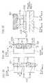
- FIGS. 1A and 1Bare a plan view of the design geometry of a semiconductor device according to a first embodiment of the present invention, and a plan view of the geometry of the semiconductor device after fabricated, respectively;
- FIGS. 2A , 2 B and 2 Care a plan view of the geometry of a gate polysilicon film provided on an element isolation region prior to the formation of an interconnect of a semiconductor device according to a second embodiment of the invention, a plan view of the geometry of the gate polysilicon film and other features after the formation of the interconnect, and a cross sectional view of the geometry thereof taken along line IIc-IIc of FIG. 2B , respectively;
- FIGS. 3A and 3Bare a plan view of a gate polysilicon film and other features of a semiconductor device according to a third embodiment of the invention, and a cross sectional view thereof taken along line IIIb-IIIb of FIG. 3A , respectively;
- FIGS. 4A and 4Bare a plan view illustrating a first modification of the third embodiment, and a cross sectional view illustrating a second modification. thereof, respectively;
- FIGS. 5A to 5Care cross sectional views illustrating parts of a manufacturing process of a semiconductor device according to a fourth embodiment of the invention, and right sides of FIGS. 5A to 5C are plan views thereof;
- FIGS. 6A , 6 B and 6 Care a plan view of the geometry of the gate polysilicon film provided on the element isolation region prior to the formation of the interconnect of the semiconductor device according to a modification of the fourth embodiment, a plan view of the geometry of the gate polysilicon film and other features after the formation of the interconnect, and a cross sectional view of the geometry thereof taken along line VIc-VIc of FIG. 6B , respectively; and
- FIGS. 7A and 7Bare a plan view illustrating the design geometry of a known semiconductor device (e.g., standard cell) and a plan view illustrating the geometry of the known semiconductor device after fabricated, respectively.
- a known semiconductor devicee.g., standard cell
- FIGS. 1A and 1Bare a plan view of the design geometry of a semiconductor device (e.g., standard cell) according to the first embodiment of the invention, and a plan view of the geometry thereof after fabricated, respectively.
- a semiconductor devicee.g., standard cell
- a gate polysilicon filmis provided across a P-type diffusion region and an N-type diffusion region which are surrounded with an element isolation region made of STI or the like.
- the gate polysilicon film G 0which is used as a gate conductor film provided across the P-type and N-type diffusion regions and the element isolation region, its parts located on the P-type and N-type diffusion regions serve as gate electrode parts (gates) G 1 , and its part located on the element isolation region serves as a gate interconnect part G 2 .
- the gate interconnect part G 2is provided with a contact C 3 for connecting the gate interconnect part G 2 to an interconnect provided in an upper level.
- the P-type diffusion regionis provided with a P-type transistor with a gate G 1 having a gate width W 1 and a gate length L
- the N-type diffusion regionis provided with an N-type transistor with a gate G 1 having a gate width W 2 and a gate length L
- the P-type diffusion regionis provided with source/drain contacts C 1 and C 2
- the N-type diffusion regionis provided with source/drain contacts C 4 and C 5 .
- the features of the design geometry of the semiconductor device according to the first embodimentreside in that a contact pad is not provided in the gate interconnect part while it is provided in the known semiconductor devices, and that the plan geometry of the gate polysilicon film G 0 is linear (rectangular).
- the contact C 3 provided on the gate polisilicon film G 0has a diameter R (especially a dimension in the gate length direction) larger than the dimension of the gate polysilicon film G 0 in the gate length direction.
- FIG. 1Billustrates the geometry of a semiconductor device which has been actually formed on the semiconductor substrate by subjecting the semiconductor device having the design geometry illustrated in FIG. 1A to a semiconductor device manufacturing process including a photolithographic step, an etching step and a resist removing step.
- the gate polysilicon film G 0 formed on the semiconductor substratemaintains a linear (rectangular) shape. This is because the design geometry of the gate polysilicon film G 0 shown in FIG. 1A has no reflex angle, and thereby no optical proximity effect occurs. Accordingly, in the semiconductor device of the first embodiment, the dimension of the gate polysilicon film in the gate length direction has a substantially constant value L′ in all over the element isolation region and the P-type and the N-type diffusion regions.
- the plan design geometry of the gate polysilicon film G 0is made linear (rectangular) and the dimension thereof in the gate length direction is made constant. Therefore, it is possible to keep the dimensions of gate electrode parts G 1 ′ in the gate length direction, which are provided on the diffusion regions, constant without widening the width of the element isolation region separating the active regions. As a result, it is possible to suppress variations in the dimension in the gate length direction due to the optical proximity effect while keeping the integration density of the semiconductor device high.
- the above first embodimenthas described the structure of the semiconductor device which suppresses variations in the gate length of the MIS transistor due to the optical proximity effect by making the gate electrode linear (rectangular) and the dimension thereof in the gate length direction constant.
- a gate polysilicon filmincludes part that provides an N-type polysilicon film on a P-type well region and part that provides a P-type polysilicon film on an N-type well region. Therefore, when the dimension of the gate polysilicon film in the gate length direction at the boundary between the N-type and the P-type polysilicon films is smaller than a certain value, the gate polysilicon film may be broken.
- a second embodiment of the inventionwill describe a structure that can maintain electrical connection even at the breakage of the gate polysilicon film while having a gate polysilicon film of linear (rectangular) plan geometry.
- FIGS. 2A , 2 B and 2 Care a plan view of the geometry of a gate polysilicon film provided on an element isolation region prior to the formation of an interconnect of a semiconductor device according to the second embodiment, a plan view of the geometry of the gate polysilicon film and a metal interconnect after the formation of the interconnect, and a cross sectional view thereof taken along line IIc-IIc of FIG. 2B , respectively.
- FIG. 2Can interlayer insulating film on which a contact is formed is not shown.
- a gate interconnect part G 12 of a gate polysilicon film G 10which is used as a linear (rectangular) gate conductor film having a constant dimension in the gate length direction includes an N-type polysilicon film G 12 a located on a P-type well region and a P-type polysilicon film G 12 b located on an N-type well region.
- a first contact C 13 ais provided on the N-type polysilicon film G 12 a and a second contact C 13 b is on the P-type polysilicon film G 12 b .
- Each diameter R of the first and the second contacts C 13 a , C 13 bis larger than the dimension L of the gate polysilicon film G 10 in the gate length direction.
- a metal interconnect M 11is formed on the first and the second contacts C 13 a , C 13 b to connect them to each other.
- the semiconductor device of the second embodimentis provided with the linear (rectangular) gate polysilicon film G 10 having the first and the second contacts C 13 a , C 13 b and the metal interconnect M 11 , whereby electrical connection between the N-type polysilicon film G 12 a and the P-type polysilicon film G 12 b can be maintained even when the boundary therebetween is broken.
- the breakage of the gate polysilicon film G 10can be prevented in the boundary region between the P-type well and the N-type well regions, i.e., between the N-type polysilicon film and the P-type polysilicon film.
- FIGS. 3A and 3Bare a plan view illustrating the plan geometry of a gate polysilicon film and a metal interconnect of a semiconductor device according to a third embodiment of the invention, and a cross sectional view thereof taken along line IIIb-IIIb of FIG. 3A , respectively.
- FIG. 3Ban interlayer insulating film on which a contact is formed is not shown.
- the third embodimentemploys, instead of the comb gate, a structure in which gate interconnect parts G 21 a to G 21 c of a plurality of linear (rectangular) gate polysilicon films G 20 a to G 20 c are electrically connected to one another via a metal interconnect M 21 .
- the gate polysilicon filmsare provided across a P-type diffusion region and an N-type diffusion region which are surrounded with an element isolation region made of STI or the like.
- the gate polysilicon films G 20 a to G 20 c formed across the P-type and the N-type diffusion regions and the element isolation regiontheir parts located on the P-type diffusion region serve as gate electrode parts (gates) G 21 a to G 21 c , respectively, and their parts located on the N-type region serve as gate interconnect parts G 22 a to G 22 c , respectively.
- the semiconductor devicehas gate contacts C 23 a to C 23 c that pass through the interlayer insulating film and is then connected to the gate interconnect parts G 22 a to G 22 c to connect an upper interconnect to the gate polysilicon films G 20 a to G 20 c .
- the semiconductor devicehas the metal interconnect M 21 that is connected to the gate contact C 23 a to C 23 c .
- the gate contacts C 23 a to C 23 chave a diameter R (especially a dimension in the gate length direction) larger than the dimension L of the gate polysilicon film G 20 in the gate length direction.
- the P-type diffusion regionis provided with a P-type MIS transistor with gates G 21 a to G 21 c having a gate width W 1 and a gate length L
- the N-type diffusion regionis provided with an N-type MIS transistor with the gates G 21 a to G 21 c having a gate width W 2 and a gate length L.
- each of the P-type and N-type diffusion regionsis provided with source/drain contacts C 26 .
- the known comb gate electrodehas a structure in which a reflex angle always exists at the connection part of each gate, which generates variations in the gate length of the MIS transistor due to the optical proximity effect in the manufacturing process.
- the plurality of gate polysilicon filmsare electrically connected to one another by the metal interconnect via the contacts provided on the gate interconnect parts, and therefore it is possible to make each gate polysilicon film linear (rectangular) and keep the constant dimension in the gate length direction. As a result, the variations in the gate length of the MIS transistor due to the optical proximity effect can be suppressed.
- FIGS. 4A and 4Bare a plan view illustrating a first modification of the third embodiment, and a cross sectional view illustrating a second modification thereof, respectively.
- a semiconductor devicehas, instead of the contacts provided on the gate interconnect parts and on part of the element isolation region located between the P-type and the. N-type diffusion regions, pairs of contacts C 23 a , C 23 a to C 23 c , C 23 c provided on the gate interconnect parts G 22 a to G 22 c and on parts of the element isolation region between which the P-type diffusion region and the N-type diffusion region are interposed.
- the semiconductor devicealso has a metal interconnect M 21 provided on the pairs of contacts C 23 a , C 23 a to C 23 c , C 23 c to electrically connect the contacts C 23 a , C 23 a to C 23 c , C 23 c to one another.
- the structures of the gate polysilicon films G 20 a to G 20 c , the P-type diffusion region and the N-type diffusion region and the source/drain contacts C 26are the same as in the third embodiment.
- each of the gate polysilicon films G 20 a to G 20 chas the boundary between the P-type polysilicon film and the N-type polysilicon film in the vicinity of the middle between the N-type and P-type well regions.
- the first modificationlike the third embodiment, it is possible to suppress the variations in the gate length of the MIS transistor which would be caused by the optical proximity effect in comb gates.
- the second embodimentit is possible to maintain electrical connection of each of the gate polysilicon films G 20 a to G 20 c even when the boundary region between the N-type polysilicon film and the P-type polysilicon film is broken.
- the gate interconnect parts G 22 a to G 22 c of the gate polysilicon films G 20 a to G 20 care electrically connected to one another via a common gate contact P 21 which is formed thereon.
- a common gate contact P 21is provided instead of the contacts C 23 a to C 23 c and the metal interconnect M 21 of the third embodiment.
- the second modificationlike the third embodiment, it is possible to suppress the variations in the gate length of the MIS transistor which would be caused by the optical proximity effect in comb gates.
- the common gate contact P 21is set to have such a dimension in the direction perpendicular to the gate length that the common gate contact P 21 is overlapped with both the N-type polysilicon film and the P-type polysilicon film in plan view.
- the semiconductor devicemay be provided with a pad formed on each gate interconnect part as in a fourth embodiment which will be described later, and a plurality of gate contacts each reaching the pad. According to this structure, the effects obtained in the third and the fourth embodiments can be achieved.
- the padis provided across the boundary region between the N-type polysilicon film and the P-type polysilicon film.
- a maskis not aligned in introducing the p-type and the n-type impurities for a dual gate into the gate polysilicon film G 20 .
- the padis set to have such a dimension in the direction perpendicular to the gate length that the pad is overlapped with both the N-type polysilicon film and the P-type polysilicon film.
- FIGS. 5A to 5Care cross sectional views illustrating parts of a manufacturing process of a semiconductor device according to a fourth embodiment of the invention, and right sides of FIGS. 5A to 5C are plan views thereof.
- the left side of each of FIGS. 5A to 5Cillustrate different cross sectional structures in different two places (i.e., on the diffusion region and the element isolation region), taken along the lines Va 1 -Va 1 and Va 2 -Va 2 in the right side of FIG. 5A , the lines Vb 1 -Vb 1 and Vb 2 -Vb 2 in the right side of FIG. 5B , and the lines Vc 1 -Vc 1 and Vc 2 -Vc 2 in the right side of FIG. 5C .
- a linear (rectangular) gate polysilicon film G 30 having a constant dimension in the gate length directionis formed across an element isolation region and active regions of a substrate.
- the gate polysilicon film G 30parts located on the active regions serve as gate electrode parts (gates) G 31 , G 31 and a part located on the element isolation region serves as a gate interconnect part G 32 .
- a thin oxide film or nitride filmis deposited on the substrate on which the gate polysilicon film G 30 is formed, the oxide film or the nitride film is then anisotropically etched to form sidewalls 35 on the side surfaces of the gate polysilicon film G 30 .
- P-type source/drain regions (P-type diffusion regions) 31 aare formed in a region of the substrate for the formation of a P-channel MIS transistor and N-type source/drain regions (N-type diffusion regions) 31 b are formed in a region of the substrate for the formation of an N-channel MIS transistor.
- a first interlayer insulating film 36 made of an oxide filmis deposited on the substrate to cover the gate polysilicon film G 30 and the sidewalls 35 , and then subjected to a planarization processing by CMP (Chemical Mechanical Polishing) or dry etching to make the top surfaces of the first interlayer insulating film 36 , the gate polysilicon film G 30 and the sidewalls 35 flush with each other.
- CMPChemical Mechanical Polishing
- a second interlayer insulating film 37 made of an oxide filmis formed on the first interlayer insulating film 36 , the gate polysilicon film G 30 and the sidewalls 35 , and a hole is formed through the second interlayer insulating film 37 and reach the gate interconnect part G 32 of the gate polysilicon film G 30 .
- This holehas a diameter larger than the dimension of the gate polysilicon film G 30 in the gate length direction and the diameter of a gate contact hole described later, and is overlapped with the N-type polysilicon film and the P-type polysilicon film of the gate polysilicon film G 30 .
- planarization processingis performed by CMP (Chemical Mechanical Polishing) or dry etching to form a pad 38 by embedding a metal film into the hole of the second interlayer insulating film 37 .
- a third interlayer insulating film 39 made of an oxide filmis formed to cover the second interlayer insulating film 37 and the pad 38 , and a gate contact hole is formed which passes through the third interlayer insulating film 39 to reach the pad 38 .
- source/drain contact holesare simultaneously formed which pass through the third interlayer insulating film 39 , the second interlayer insulating film 37 and the first interlayer insulating film 36 and reach the P-type source/drain regions 31 a and the N-type source/drain regions 31 b .
- the contact holesare filled with tungsten or the like to form a gate contact 40 and source/drain contacts 41 a and 41 b.
- the gate polysilicon film G 30is linear (rectangular) and has a constant dimension in the gate length direction. Thus, if the contact hole formation step shown in FIG. 5C is performed directly, the gate contact hole reaching the gate interconnect part G 32 may pass through the first interlayer insulating film 36 and the element isolation region to reach the well regions.
- the pad 38is formed on the gate interconnect part G 32 to have a diameter larger than the dimension of the gate polysilicon film G 30 in the gate length direction and the diameter of the gate contact, followed by simultaneous formation of the gate contact hole and the source/drain contact holes. Therefore, it is possible to definitely prevent the gate contact hole from reaching the element isolation region in spite of the linear gate polysilicon film G 30 having a constant dimension in the gate length direction.
- the maskis not aligned in introducing p-type and n-type impurities for a dual gate into the gate polysilicon film G 30 .
- the size of the pad 38is set such that the pad 38 is overlapped with both the N-type polysilicon film and the P-type polysilicon film.
- FIGS. 6A , 6 B and 6 Care a plan view of the geometry of the gate polysilicon film provided on the element isolation region prior to the formation of the interconnect of the semiconductor device according to the modification of the fourth embodiment, a plan view of the geometry of the gate polysilicon film and the metal interconnect after the formation of the interconnect, and a cross sectional view thereof taken along line VIc-VIc of FIG. 6B , respectively.
- FIG. 6Cthe interlayer insulating film on which the contact is formed is not shown.
- a gate interconnect part G 42 of a linear (rectangular) gate polysilicon film G 40has an N-type polysilicon film G 42 a located on a P-type well region and a P-type polysilicon film G 42 b located on an N-type well region.
- a first contact C 43 ais provided via a pad P 41 a on the N-type polysilicon film G 42 a
- a second contact C 43 bis provided via a pad P 41 b on the P-type polysilicon film G 42 b .
- the diameter R of the first and the second contacts C 43 a , C 43 bis larger than the dimension L of the gate polysilicon film G 40 in the gate length direction, and the diameter of the pads P 41 a , P 41 b is larger than the diameter R of the first and the second contacts C 43 a , C 43 b.
- a metal interconnect M 41is formed on the first and the second contacts C 43 a , C 43 b to electrically connect them to each other.
- the first and the second contacts C 43 a , C 43 b and the metal interconnect M 41ensure electrical connection between the N-type polysilicon film G 42 a and the P-type polysilicon film G 42 b even when the boundary between the N-type polysilicon film G 42 a and the P-type polysilicon film G 42 b is broken because of the linear (rectangular) gate polysilicon film G 40 .
- the breakage of the gate polysilicon film G 40 in the boundary region between the P-type well and the N-type well regions, i.e., between the N-type polysilicon film and the P-type polysilicon film,can be compensated for, even when the gate polysilicon film G 40 has a linear (rectangular) plan geometry and a constant dimension in the gate length direction.
- the gate polysilicon filmis used as the gate conductor film, but the gate conductor film of the present invention is not limited to the polysilicon film.
- the gate conductor filmmay be other conductor films such as a metal film or a polymetallic film in which metal films and polysilicon films are stacked. Also in these cases, the same effects as in each embodiment can be achieved.
- upper portions of the gate polysilicon film and the source/drain regionsare in general silicified by a so-called salicide process in employing the present invention although the description is omitted in each embodiment.
- the semiconductor device of the present inventioncan be used for LSIs which are mounted on various electronics, in particular for an LSI with high performance in which variations in the gate length of a MIS transistor are small.
Landscapes
- Engineering & Computer Science (AREA)
- Physics & Mathematics (AREA)
- Condensed Matter Physics & Semiconductors (AREA)
- General Physics & Mathematics (AREA)
- Manufacturing & Machinery (AREA)
- Computer Hardware Design (AREA)
- Microelectronics & Electronic Packaging (AREA)
- Power Engineering (AREA)
- Metal-Oxide And Bipolar Metal-Oxide Semiconductor Integrated Circuits (AREA)
- Internal Circuitry In Semiconductor Integrated Circuit Devices (AREA)
- Electrodes Of Semiconductors (AREA)
Abstract
Description
Claims (11)
Priority Applications (1)
| Application Number | Priority Date | Filing Date | Title |
|---|---|---|---|
| US11/892,053US7709900B2 (en) | 2004-07-22 | 2007-08-20 | Semiconductor device |
Applications Claiming Priority (2)
| Application Number | Priority Date | Filing Date | Title |
|---|---|---|---|
| JP2004-213903 | 2004-07-22 | ||
| JP2004213903AJP4175649B2 (en) | 2004-07-22 | 2004-07-22 | Semiconductor device |
Related Child Applications (1)
| Application Number | Title | Priority Date | Filing Date |
|---|---|---|---|
| US11/892,053DivisionUS7709900B2 (en) | 2004-07-22 | 2007-08-20 | Semiconductor device |
Publications (2)
| Publication Number | Publication Date |
|---|---|
| US20060017070A1 US20060017070A1 (en) | 2006-01-26 |
| US7279727B2true US7279727B2 (en) | 2007-10-09 |
Family
ID=35656210
Family Applications (2)
| Application Number | Title | Priority Date | Filing Date |
|---|---|---|---|
| US11/148,208Active2026-03-06US7279727B2 (en) | 2004-07-22 | 2005-06-09 | Semiconductor device |
| US11/892,053Expired - LifetimeUS7709900B2 (en) | 2004-07-22 | 2007-08-20 | Semiconductor device |
Family Applications After (1)
| Application Number | Title | Priority Date | Filing Date |
|---|---|---|---|
| US11/892,053Expired - LifetimeUS7709900B2 (en) | 2004-07-22 | 2007-08-20 | Semiconductor device |
Country Status (3)
| Country | Link |
|---|---|
| US (2) | US7279727B2 (en) |
| JP (1) | JP4175649B2 (en) |
| CN (1) | CN100539144C (en) |
Cited By (26)
| Publication number | Priority date | Publication date | Assignee | Title |
|---|---|---|---|---|
| US20080042214A1 (en)* | 2004-07-22 | 2008-02-21 | Matsushita Electric Industrial Co., Ltd. | Semiconductor device |
| US20100187627A1 (en)* | 2008-03-13 | 2010-07-29 | Tela Innovations, Inc. | Channelized Gate Level Cross-Coupled Transistor Device with Overlapping PMOS Transistors and Overlapping NMOS Transistors Relative to Direction of Gate Electrodes |
| US20110133253A1 (en)* | 2009-10-19 | 2011-06-09 | Panasonic Corporation | Semiconductor device |
| US20110193170A1 (en)* | 2010-02-11 | 2011-08-11 | United Microelectronics Corporation | Electro-Static Discharge (ESD) Clamping Device |
| US20120292666A1 (en)* | 2010-03-05 | 2012-11-22 | Panasonic Corporation | Semiconductor device |
| US20130161760A1 (en)* | 2006-03-09 | 2013-06-27 | Scott T. Becker | Integrated Circuit Including Gate Electrode Tracks Including Offset End-to-End Spacings |
| US8541879B2 (en) | 2007-12-13 | 2013-09-24 | Tela Innovations, Inc. | Super-self-aligned contacts and method for making the same |
| US8549455B2 (en) | 2007-08-02 | 2013-10-01 | Tela Innovations, Inc. | Methods for cell phasing and placement in dynamic array architecture and implementation of the same |
| US8653857B2 (en) | 2006-03-09 | 2014-02-18 | Tela Innovations, Inc. | Circuitry and layouts for XOR and XNOR logic |
| US8661392B2 (en) | 2009-10-13 | 2014-02-25 | Tela Innovations, Inc. | Methods for cell boundary encroachment and layouts implementing the Same |
| US8658542B2 (en) | 2006-03-09 | 2014-02-25 | Tela Innovations, Inc. | Coarse grid design methods and structures |
| US8667443B2 (en) | 2007-03-05 | 2014-03-04 | Tela Innovations, Inc. | Integrated circuit cell library for multiple patterning |
| US8680626B2 (en) | 2007-10-26 | 2014-03-25 | Tela Innovations, Inc. | Methods, structures, and designs for self-aligning local interconnects used in integrated circuits |
| US8701071B2 (en) | 2008-01-31 | 2014-04-15 | Tela Innovations, Inc. | Enforcement of semiconductor structure regularity for localized transistors and interconnect |
| US8756551B2 (en) | 2007-08-02 | 2014-06-17 | Tela Innovations, Inc. | Methods for designing semiconductor device with dynamic array section |
| US8759985B2 (en) | 2008-03-27 | 2014-06-24 | Tela Innovations, Inc. | Methods for multi-wire routing and apparatus implementing same |
| US8839175B2 (en) | 2006-03-09 | 2014-09-16 | Tela Innovations, Inc. | Scalable meta-data objects |
| US8863063B2 (en) | 2009-05-06 | 2014-10-14 | Tela Innovations, Inc. | Finfet transistor circuit |
| US9035359B2 (en) | 2006-03-09 | 2015-05-19 | Tela Innovations, Inc. | Semiconductor chip including region including linear-shaped conductive structures forming gate electrodes and having electrical connection areas arranged relative to inner region between transistors of different types and associated methods |
| US9122832B2 (en) | 2008-08-01 | 2015-09-01 | Tela Innovations, Inc. | Methods for controlling microloading variation in semiconductor wafer layout and fabrication |
| US9159627B2 (en) | 2010-11-12 | 2015-10-13 | Tela Innovations, Inc. | Methods for linewidth modification and apparatus implementing the same |
| US9230910B2 (en) | 2006-03-09 | 2016-01-05 | Tela Innovations, Inc. | Oversized contacts and vias in layout defined by linearly constrained topology |
| US9449970B2 (en) | 2014-08-22 | 2016-09-20 | Samsung Electronics Co., Ltd. | Semiconductor devices and methods of forming the same |
| US9563733B2 (en) | 2009-05-06 | 2017-02-07 | Tela Innovations, Inc. | Cell circuit and layout with linear finfet structures |
| US9754878B2 (en) | 2006-03-09 | 2017-09-05 | Tela Innovations, Inc. | Semiconductor chip including a chip level based on a layout that includes both regular and irregular wires |
| US10276488B2 (en) | 2012-06-01 | 2019-04-30 | Taiwan Semiconductor Manufacturing Company, Ltd. | Method of fabricating field effect transistor having non-orthogonal gate electrode |
Families Citing this family (11)
| Publication number | Priority date | Publication date | Assignee | Title |
|---|---|---|---|---|
| JP2006054430A (en)* | 2004-07-12 | 2006-02-23 | Renesas Technology Corp | Semiconductor device |
| WO2008029334A1 (en)* | 2006-09-04 | 2008-03-13 | Nxp B.V. | Fabrication of self-assembled nanowire-type interconnects on a semiconductor device |
| JP2009152437A (en)* | 2007-12-21 | 2009-07-09 | Nec Electronics Corp | Semiconductor device |
| US8018000B2 (en)* | 2008-01-11 | 2011-09-13 | Taiwan Semiconductor Manufacturing Company, Ltd. | Electrostatic discharge protection pattern for high voltage applications |
| JP2010050311A (en)* | 2008-08-22 | 2010-03-04 | Elpida Memory Inc | Semiconductor device, and method of manufacturing the same |
| JP2010118410A (en)* | 2008-11-11 | 2010-05-27 | Nec Electronics Corp | Semiconductor device |
| GB2466313A (en) | 2008-12-22 | 2010-06-23 | Cambridge Silicon Radio Ltd | Radio Frequency CMOS Transistor |
| JP6083930B2 (en) | 2012-01-18 | 2017-02-22 | キヤノン株式会社 | Photoelectric conversion device, imaging system, and method of manufacturing photoelectric conversion device |
| US20150061076A1 (en)* | 2013-08-27 | 2015-03-05 | International Business Machines Corporation | High density resistor |
| US9640444B2 (en) | 2014-07-23 | 2017-05-02 | Samsung Electronics Co., Ltd. | Semiconductor device and method of fabricating the same |
| EP3113477B1 (en)* | 2015-06-30 | 2017-08-02 | Axis AB | Monitoring camera |
Citations (5)
| Publication number | Priority date | Publication date | Assignee | Title |
|---|---|---|---|---|
| US5420447A (en)* | 1993-01-29 | 1995-05-30 | Sgs-Thomson Microelectronics, Inc. | Double buffer base gate array cell |
| US5498897A (en)* | 1994-07-01 | 1996-03-12 | Texas Instruments Incorporated | Transistor layout for semiconductor integrated circuit |
| JPH08272075A (en) | 1995-03-06 | 1996-10-18 | Lsi Logic Corp | System and method for optical proximity correction on macrocell library |
| JPH1032253A (en) | 1996-07-15 | 1998-02-03 | Toshiba Corp | Semiconductor device and its manufacturing method, basic cell library and its forming method, mask |
| JP2002026125A (en) | 2000-07-10 | 2002-01-25 | Mitsubishi Electric Corp | Semiconductor device |
Family Cites Families (13)
| Publication number | Priority date | Publication date | Assignee | Title |
|---|---|---|---|---|
| JPS6450443U (en) | 1987-09-24 | 1989-03-29 | ||
| JPS6489468A (en) | 1987-09-30 | 1989-04-03 | Toshiba Corp | Semiconductor device |
| JPH056965A (en) | 1991-06-26 | 1993-01-14 | Nec Ic Microcomput Syst Ltd | Semiconductor integrated circuit and manufacture thereof |
| JPH05251649A (en) | 1991-12-20 | 1993-09-28 | Nippon Steel Corp | MOS semiconductor device and method of manufacturing the same |
| JPH09246541A (en) | 1996-03-07 | 1997-09-19 | Sony Corp | Manufacture of semiconductor device |
| JPH11297850A (en) | 1998-04-15 | 1999-10-29 | Hitachi Ltd | Semiconductor integrated circuit device and method of manufacturing the same |
| JP3394022B2 (en) | 1999-08-16 | 2003-04-07 | 松下電器産業株式会社 | Semiconductor device and manufacturing method thereof |
| JP2001168212A (en) | 1999-12-07 | 2001-06-22 | Mitsubishi Electric Corp | Semiconductor storage device |
| US6376351B1 (en)* | 2001-06-28 | 2002-04-23 | Taiwan Semiconductor Manufacturing Company | High Fmax RF MOSFET with embedded stack gate |
| JP2003218117A (en) | 2002-01-28 | 2003-07-31 | Mitsubishi Electric Corp | Semiconductor device manufacturing method and semiconductor device |
| KR100553682B1 (en)* | 2003-03-07 | 2006-02-24 | 삼성전자주식회사 | A semiconductor device having a gate electrode and a method of forming the same |
| JP4175649B2 (en)* | 2004-07-22 | 2008-11-05 | 松下電器産業株式会社 | Semiconductor device |
| JP2007073709A (en) | 2005-09-06 | 2007-03-22 | Nec Electronics Corp | Semiconductor device |
- 2004
- 2004-07-22JPJP2004213903Apatent/JP4175649B2/ennot_activeExpired - Lifetime
- 2005
- 2005-06-09USUS11/148,208patent/US7279727B2/enactiveActive
- 2005-07-20CNCNB2005100859849Apatent/CN100539144C/ennot_activeExpired - Lifetime
- 2007
- 2007-08-20USUS11/892,053patent/US7709900B2/ennot_activeExpired - Lifetime
Patent Citations (6)
| Publication number | Priority date | Publication date | Assignee | Title |
|---|---|---|---|---|
| US5420447A (en)* | 1993-01-29 | 1995-05-30 | Sgs-Thomson Microelectronics, Inc. | Double buffer base gate array cell |
| US5498897A (en)* | 1994-07-01 | 1996-03-12 | Texas Instruments Incorporated | Transistor layout for semiconductor integrated circuit |
| JPH08272075A (en) | 1995-03-06 | 1996-10-18 | Lsi Logic Corp | System and method for optical proximity correction on macrocell library |
| JPH1032253A (en) | 1996-07-15 | 1998-02-03 | Toshiba Corp | Semiconductor device and its manufacturing method, basic cell library and its forming method, mask |
| US5847421A (en)* | 1996-07-15 | 1998-12-08 | Kabushiki Kaisha Toshiba | Logic cell having efficient optical proximity effect correction |
| JP2002026125A (en) | 2000-07-10 | 2002-01-25 | Mitsubishi Electric Corp | Semiconductor device |
Cited By (124)
| Publication number | Priority date | Publication date | Assignee | Title |
|---|---|---|---|---|
| US20080042214A1 (en)* | 2004-07-22 | 2008-02-21 | Matsushita Electric Industrial Co., Ltd. | Semiconductor device |
| US7709900B2 (en)* | 2004-07-22 | 2010-05-04 | Panasonic Corporation | Semiconductor device |
| US9589091B2 (en) | 2006-03-09 | 2017-03-07 | Tela Innovations, Inc. | Scalable meta-data objects |
| US8946781B2 (en) | 2006-03-09 | 2015-02-03 | Tela Innovations, Inc. | Integrated circuit including gate electrode conductive structures with different extension distances beyond contact |
| US10230377B2 (en) | 2006-03-09 | 2019-03-12 | Tela Innovations, Inc. | Circuitry and layouts for XOR and XNOR logic |
| US10217763B2 (en) | 2006-03-09 | 2019-02-26 | Tela Innovations, Inc. | Semiconductor chip having region including gate electrode features of rectangular shape on gate horizontal grid and first-metal structures of rectangular shape on at least eight first-metal gridlines of first-metal vertical grid |
| US10186523B2 (en) | 2006-03-09 | 2019-01-22 | Tela Innovations, Inc. | Semiconductor chip having region including gate electrode features formed in part from rectangular layout shapes on gate horizontal grid and first-metal structures formed in part from rectangular layout shapes on at least eight first-metal gridlines of first-metal vertical grid |
| US10141334B2 (en) | 2006-03-09 | 2018-11-27 | Tela Innovations, Inc. | Semiconductor chip including region having rectangular-shaped gate structures and first-metal structures |
| US8952425B2 (en) | 2006-03-09 | 2015-02-10 | Tela Innovations, Inc. | Integrated circuit including at least four linear-shaped conductive structures having extending portions of different length |
| US20130168777A1 (en)* | 2006-03-09 | 2013-07-04 | Scott T. Becker | Integrated Circuit Including Gate Electrode Tracks Forming Gate Electrodes of Different Transistor Types and Linear Shaped Conductor Electrically Connecting Gate Electrodes |
| US20130168778A1 (en)* | 2006-03-09 | 2013-07-04 | Scott T. Becker | Integrated Circuit Including Gate Electrode Tracks That Each Form Gate Electrodes of Different Transistor Types With Intervening Non-Gate-Forming Gate Electrode Track |
| US10141335B2 (en) | 2006-03-09 | 2018-11-27 | Tela Innovations, Inc. | Semiconductor CIP including region having rectangular-shaped gate structures and first metal structures |
| US8823062B2 (en) | 2006-03-09 | 2014-09-02 | Tela Innovations, Inc. | Integrated circuit with offset line end spacings in linear gate electrode level |
| US9917056B2 (en)* | 2006-03-09 | 2018-03-13 | Tela Innovations, Inc. | Coarse grid design methods and structures |
| US9905576B2 (en) | 2006-03-09 | 2018-02-27 | Tela Innovations, Inc. | Semiconductor chip including region having rectangular-shaped gate structures and first metal structures |
| US9859277B2 (en) | 2006-03-09 | 2018-01-02 | Tela Innovations, Inc. | Methods, structures, and designs for self-aligning local interconnects used in integrated circuits |
| US9754878B2 (en) | 2006-03-09 | 2017-09-05 | Tela Innovations, Inc. | Semiconductor chip including a chip level based on a layout that includes both regular and irregular wires |
| US9741719B2 (en) | 2006-03-09 | 2017-08-22 | Tela Innovations, Inc. | Methods, structures, and designs for self-aligning local interconnects used in integrated circuits |
| US20170186771A1 (en)* | 2006-03-09 | 2017-06-29 | Tela Innovations, Inc. | Semiconductor Chip and Method for Manufacturing the Same |
| US9711495B2 (en) | 2006-03-09 | 2017-07-18 | Tela Innovations, Inc. | Oversized contacts and vias in layout defined by linearly constrained topology |
| US9425272B2 (en) | 2006-03-09 | 2016-08-23 | Tela Innovations, Inc. | Semiconductor chip including integrated circuit including four transistors of first transistor type and four transistors of second transistor type with electrical connections between various transistors and methods for manufacturing the same |
| US8839175B2 (en) | 2006-03-09 | 2014-09-16 | Tela Innovations, Inc. | Scalable meta-data objects |
| US20170053937A1 (en)* | 2006-03-09 | 2017-02-23 | Tela Innovations, Inc. | Semiconductor Chip and Method for Manufacturing the Same |
| US9443947B2 (en) | 2006-03-09 | 2016-09-13 | Tela Innovations, Inc. | Semiconductor chip including region having integrated circuit transistor gate electrodes formed by various conductive structures of specified shape and position and method for manufacturing the same |
| US8653857B2 (en) | 2006-03-09 | 2014-02-18 | Tela Innovations, Inc. | Circuitry and layouts for XOR and XNOR logic |
| US20160254223A1 (en)* | 2006-03-09 | 2016-09-01 | Tela Innovations, Inc. | Coarse Grid Design Methods and Structures |
| US8658542B2 (en) | 2006-03-09 | 2014-02-25 | Tela Innovations, Inc. | Coarse grid design methods and structures |
| US8921896B2 (en) | 2006-03-09 | 2014-12-30 | Tela Innovations, Inc. | Integrated circuit including linear gate electrode structures having different extension distances beyond contact |
| US9425145B2 (en) | 2006-03-09 | 2016-08-23 | Tela Innovations, Inc. | Oversized contacts and vias in layout defined by linearly constrained topology |
| US9425273B2 (en) | 2006-03-09 | 2016-08-23 | Tela Innovations, Inc. | Semiconductor chip including integrated circuit including at least five gate level conductive structures having particular spatial and electrical relationship and method for manufacturing the same |
| US9673825B2 (en) | 2006-03-09 | 2017-06-06 | Tela Innovations, Inc. | Circuitry and layouts for XOR and XNOR logic |
| US9336344B2 (en) | 2006-03-09 | 2016-05-10 | Tela Innovations, Inc. | Coarse grid design methods and structures |
| US9240413B2 (en) | 2006-03-09 | 2016-01-19 | Tela Innovations, Inc. | Methods, structures, and designs for self-aligning local interconnects used in integrated circuits |
| US9230910B2 (en) | 2006-03-09 | 2016-01-05 | Tela Innovations, Inc. | Oversized contacts and vias in layout defined by linearly constrained topology |
| US9035359B2 (en) | 2006-03-09 | 2015-05-19 | Tela Innovations, Inc. | Semiconductor chip including region including linear-shaped conductive structures forming gate electrodes and having electrical connection areas arranged relative to inner region between transistors of different types and associated methods |
| US9009641B2 (en) | 2006-03-09 | 2015-04-14 | Tela Innovations, Inc. | Circuits with linear finfet structures |
| US20130161760A1 (en)* | 2006-03-09 | 2013-06-27 | Scott T. Becker | Integrated Circuit Including Gate Electrode Tracks Including Offset End-to-End Spacings |
| US8921897B2 (en) | 2006-03-09 | 2014-12-30 | Tela Innovations, Inc. | Integrated circuit with gate electrode conductive structures having offset ends |
| US10074640B2 (en) | 2007-03-05 | 2018-09-11 | Tela Innovations, Inc. | Integrated circuit cell library for multiple patterning |
| US8667443B2 (en) | 2007-03-05 | 2014-03-04 | Tela Innovations, Inc. | Integrated circuit cell library for multiple patterning |
| US9633987B2 (en) | 2007-03-05 | 2017-04-25 | Tela Innovations, Inc. | Integrated circuit cell library for multiple patterning |
| US9595515B2 (en) | 2007-03-07 | 2017-03-14 | Tela Innovations, Inc. | Semiconductor chip including integrated circuit defined within dynamic array section |
| US9910950B2 (en) | 2007-03-07 | 2018-03-06 | Tela Innovations, Inc. | Methods for cell phasing and placement in dynamic array architecture and implementation of the same |
| US9424387B2 (en) | 2007-03-07 | 2016-08-23 | Tela Innovations, Inc. | Methods for cell phasing and placement in dynamic array architecture and implementation of the same |
| US8966424B2 (en) | 2007-03-07 | 2015-02-24 | Tela Innovations, Inc. | Methods for cell phasing and placement in dynamic array architecture and implementation of the same |
| US8549455B2 (en) | 2007-08-02 | 2013-10-01 | Tela Innovations, Inc. | Methods for cell phasing and placement in dynamic array architecture and implementation of the same |
| US8756551B2 (en) | 2007-08-02 | 2014-06-17 | Tela Innovations, Inc. | Methods for designing semiconductor device with dynamic array section |
| US8759882B2 (en) | 2007-08-02 | 2014-06-24 | Tela Innovations, Inc. | Semiconductor device with dynamic array sections defined and placed according to manufacturing assurance halos |
| US10734383B2 (en) | 2007-10-26 | 2020-08-04 | Tela Innovations, Inc. | Methods, structures, and designs for self-aligning local interconnects used in integrated circuits |
| US8680626B2 (en) | 2007-10-26 | 2014-03-25 | Tela Innovations, Inc. | Methods, structures, and designs for self-aligning local interconnects used in integrated circuits |
| US8951916B2 (en) | 2007-12-13 | 2015-02-10 | Tela Innovations, Inc. | Super-self-aligned contacts and method for making the same |
| US8541879B2 (en) | 2007-12-13 | 2013-09-24 | Tela Innovations, Inc. | Super-self-aligned contacts and method for making the same |
| US9818747B2 (en) | 2007-12-13 | 2017-11-14 | Tela Innovations, Inc. | Super-self-aligned contacts and method for making the same |
| US10461081B2 (en) | 2007-12-13 | 2019-10-29 | Tel Innovations, Inc. | Super-self-aligned contacts and method for making the same |
| US9281371B2 (en) | 2007-12-13 | 2016-03-08 | Tela Innovations, Inc. | Super-self-aligned contacts and method for making the same |
| US9530734B2 (en) | 2008-01-31 | 2016-12-27 | Tela Innovations, Inc. | Enforcement of semiconductor structure regularity for localized transistors and interconnect |
| US8701071B2 (en) | 2008-01-31 | 2014-04-15 | Tela Innovations, Inc. | Enforcement of semiconductor structure regularity for localized transistors and interconnect |
| US9202779B2 (en) | 2008-01-31 | 2015-12-01 | Tela Innovations, Inc. | Enforcement of semiconductor structure regularity for localized transistors and interconnect |
| US8669595B2 (en) | 2008-03-13 | 2014-03-11 | Tela Innovations, Inc. | Integrated circuit including cross-coupled transistors having gate electrodes formed within gate level feature layout channels with gate contact position, alignment, and offset specifications |
| US8587034B2 (en) | 2008-03-13 | 2013-11-19 | Tela Innovations, Inc. | Integrated circuit including cross-coupled transistors having gate electrodes formed within gate level feature layout channels with four inside positioned gate contacts and electrical connection of transistor gates through linear interconnect conductors in single interconnect layer |
| US8872283B2 (en) | 2008-03-13 | 2014-10-28 | Tela Innovations, Inc. | Integrated circuit including cross-coupled transistors having gate electrodes formed within gate level feature layout channels with shared diffusion regions on opposite sides of two-transistor-forming gate level feature |
| US8742463B2 (en) | 2008-03-13 | 2014-06-03 | Tela Innovations, Inc. | Integrated circuit including cross-coupled transistors having gate electrodes formed within gate level feature layout channels with outer positioned gate contacts |
| US8735995B2 (en) | 2008-03-13 | 2014-05-27 | Tela Innovations, Inc. | Cross-coupled transistor circuit defined on three gate electrode tracks with diffusion regions of common node on opposing sides of same gate electrode track |
| US8735944B2 (en) | 2008-03-13 | 2014-05-27 | Tela Innovations, Inc. | Integrated circuit including cross-coupled transistors having gate electrodes formed within gate level feature layout channels with serially connected transistors |
| US8581303B2 (en) | 2008-03-13 | 2013-11-12 | Tela Innovations, Inc. | Integrated circuit including cross-coupled trasistors having gate electrodes formed within gate level feature layout channels with four inside positioned gate contacts having offset relationships and electrical connection of cross-coupled transistors through same interconnect layer |
| US8729606B2 (en) | 2008-03-13 | 2014-05-20 | Tela Innovations, Inc. | Integrated circuit including cross-coupled transistors having gate electrodes formed within gate level feature layout channels |
| US8729643B2 (en) | 2008-03-13 | 2014-05-20 | Tela Innovations, Inc. | Cross-coupled transistor circuit including offset inner gate contacts |
| US9081931B2 (en) | 2008-03-13 | 2015-07-14 | Tela Innovations, Inc. | Cross-coupled transistor circuit having diffusion regions of common node on opposing sides of same gate electrode track and gate node connection through single interconnect layer |
| US9117050B2 (en) | 2008-03-13 | 2015-08-25 | Tela Innovations, Inc. | Integrated circuit including cross-coupled transistors having gate electrodes formed within gate level feature layout channels with gate contact position and offset specifications |
| US8772839B2 (en) | 2008-03-13 | 2014-07-08 | Tela Innovations, Inc. | Integrated circuit including cross-coupled transistors having gate electrodes formed within gate level feature layout channels with four inside positioned gate contacts having offset and aligned relationships and electrical connection of transistor gates through linear interconnect conductors in single interconnect layer |
| US10727252B2 (en) | 2008-03-13 | 2020-07-28 | Tela Innovations, Inc. | Semiconductor chip including integrated circuit having cross-coupled transistor configuration and method for manufacturing the same |
| US8866197B2 (en) | 2008-03-13 | 2014-10-21 | Tela Innovations, Inc. | Integrated circuit including cross-coupled transistors having gate electrodes formed within gate level feature layout channels with at least two gate electrodes electrically connected to each other through another transistor forming gate level feature |
| US9208279B2 (en) | 2008-03-13 | 2015-12-08 | Tela Innovations, Inc. | Semiconductor chip including digital logic circuit including linear-shaped conductive structures having electrical connection areas located within inner region between transistors of different type and associated methods |
| US9213792B2 (en) | 2008-03-13 | 2015-12-15 | Tela Innovations, Inc. | Semiconductor chip including digital logic circuit including at least six transistors with some transistors forming cross-coupled transistor configuration and associated methods |
| US10658385B2 (en) | 2008-03-13 | 2020-05-19 | Tela Innovations, Inc. | Cross-coupled transistor circuit defined on four gate electrode tracks |
| US8680583B2 (en) | 2008-03-13 | 2014-03-25 | Tela Innovations, Inc. | Integrated circuit including cross-coupled transistors having gate electrodes formed within at least nine gate level feature layout channels |
| US9245081B2 (en) | 2008-03-13 | 2016-01-26 | Tela Innovations, Inc. | Semiconductor chip including digital logic circuit including at least nine linear-shaped conductive structures collectively forming gate electrodes of at least six transistors with some transistors forming cross-coupled transistor configuration and associated methods |
| US10651200B2 (en) | 2008-03-13 | 2020-05-12 | Tela Innovations, Inc. | Cross-coupled transistor circuit defined on three gate electrode tracks |
| US8853793B2 (en) | 2008-03-13 | 2014-10-07 | Tela Innovations, Inc. | Integrated circuit including gate electrode level region including cross-coupled transistors having gate contacts located over inner portion of gate electrode level region and offset gate level feature line ends |
| US8853794B2 (en) | 2008-03-13 | 2014-10-07 | Tela Innovations, Inc. | Integrated circuit within semiconductor chip including cross-coupled transistor configuration |
| US8785979B2 (en) | 2008-03-13 | 2014-07-22 | Tela Innovations, Inc. | Integrated circuit including cross-coupled transistors having gate electrodes formed within gate level feature layout channels with two inside positioned gate contacts and two outside positioned gate contacts and electrical connection of cross-coupled transistors through same interconnect layer |
| US8847329B2 (en) | 2008-03-13 | 2014-09-30 | Tela Innovations, Inc. | Cross-coupled transistor circuit defined having diffusion regions of common node on opposing sides of same gate electrode track with at least two non-inner positioned gate contacts |
| US8669594B2 (en) | 2008-03-13 | 2014-03-11 | Tela Innovations, Inc. | Integrated circuit including cross-coupled transistors having gate electrodes formed within at least twelve gate level feature layout channels |
| US8847331B2 (en) | 2008-03-13 | 2014-09-30 | Tela Innovations, Inc. | Semiconductor chip including region having cross-coupled transistor configuration with offset electrical connection areas on gate electrode forming conductive structures and at least two different inner extension distances of gate electrode forming conductive structures |
| US8785978B2 (en) | 2008-03-13 | 2014-07-22 | Tela Innovations, Inc. | Integrated circuit including cross-coupled transistors having gate electrodes formed within gate level feature layout channels with electrical connection of cross-coupled transistors through same interconnect layer |
| US10020321B2 (en) | 2008-03-13 | 2018-07-10 | Tela Innovations, Inc. | Cross-coupled transistor circuit defined on two gate electrode tracks |
| US8592872B2 (en) | 2008-03-13 | 2013-11-26 | Tela Innovations, Inc. | Integrated circuit including cross-coupled transistors with two transistors of different type having gate electrodes formed by common gate level feature with shared diffusion regions on opposite sides of common gate level feature |
| US8816402B2 (en) | 2008-03-13 | 2014-08-26 | Tela Innovations, Inc. | Integrated circuit including cross-coupled transistors having gate electrodes formed within gate level feature layout channels with gate level feature layout channel including single transistor |
| US8836045B2 (en) | 2008-03-13 | 2014-09-16 | Tela Innovations, Inc. | Cross-coupled transistor circuit having diffusion regions of common node on opposing sides of same gate electrode track |
| US8552509B2 (en) | 2008-03-13 | 2013-10-08 | Tela Innovations, Inc. | Integrated circuit including cross-coupled transistors having gate electrodes formed within gate level feature layout channels with other transistors positioned between cross-coupled transistors |
| US9536899B2 (en) | 2008-03-13 | 2017-01-03 | Tela Innovations, Inc. | Semiconductor chip including integrated circuit having cross-coupled transistor configuration and method for manufacturing the same |
| US9871056B2 (en) | 2008-03-13 | 2018-01-16 | Tela Innovations, Inc. | Semiconductor chip including integrated circuit having cross-coupled transistor configuration and method for manufacturing the same |
| US8742462B2 (en) | 2008-03-13 | 2014-06-03 | Tela Innovations, Inc. | Integrated circuit including cross-coupled transistors having gate electrodes formed within gate level feature layout channels with gate contact position specifications |
| US20100187627A1 (en)* | 2008-03-13 | 2010-07-29 | Tela Innovations, Inc. | Channelized Gate Level Cross-Coupled Transistor Device with Overlapping PMOS Transistors and Overlapping NMOS Transistors Relative to Direction of Gate Electrodes |
| US8552508B2 (en) | 2008-03-13 | 2013-10-08 | Tela Innovations, Inc. | Integrated circuit including cross-coupled transistors having gate electrodes formed within gate level feature layout channels with shared diffusion regions on opposite sides of two-transistor-forming gate level feature and electrical connection of transistor gates through linear interconnect conductors in single interconnect layer |
| US8581304B2 (en) | 2008-03-13 | 2013-11-12 | Tela Innovations, Inc. | Integrated circuit including cross-coupled transistors having gate electrodes formed within gate level feature layout channels with four inside positioned gate contacts having offset and aligned relationships |
| US8835989B2 (en) | 2008-03-13 | 2014-09-16 | Tela Innovations, Inc. | Integrated circuit including cross-coupled transistors having gate electrodes formed within gate level feature layout channels with gate electrode placement specifications |
| US8575706B2 (en) | 2008-03-13 | 2013-11-05 | Tela Innovations, Inc. | Integrated circuit including cross-coupled transistors having gate electrodes formed within gate level feature layout channels with at least two different gate level features inner extensions beyond gate electrode |
| US8558322B2 (en) | 2008-03-13 | 2013-10-15 | Tela Innovations, Inc. | Integrated circuit including cross-coupled transistors having gate electrodes formed within gate level feature layout channels with at least two gate electrodes electrically connected to each other through gate level feature |
| US8569841B2 (en) | 2008-03-13 | 2013-10-29 | Tela Innovations, Inc. | Integrated circuit including cross-coupled transistors having gate electrodes formed within gate level feature layout channels with at least one gate level feature extending into adjacent gate level feature layout channel |
| US8564071B2 (en) | 2008-03-13 | 2013-10-22 | Tela Innovations, Inc. | Integrated circuit including cross-coupled transistors having gate electrodes formed within gate level feature layout channels with at least two different gate level feature extensions beyond contact |
| US9779200B2 (en) | 2008-03-27 | 2017-10-03 | Tela Innovations, Inc. | Methods for multi-wire routing and apparatus implementing same |
| US8759985B2 (en) | 2008-03-27 | 2014-06-24 | Tela Innovations, Inc. | Methods for multi-wire routing and apparatus implementing same |
| US9390215B2 (en) | 2008-03-27 | 2016-07-12 | Tela Innovations, Inc. | Methods for multi-wire routing and apparatus implementing same |
| US9122832B2 (en) | 2008-08-01 | 2015-09-01 | Tela Innovations, Inc. | Methods for controlling microloading variation in semiconductor wafer layout and fabrication |
| US10446536B2 (en) | 2009-05-06 | 2019-10-15 | Tela Innovations, Inc. | Cell circuit and layout with linear finfet structures |
| US9563733B2 (en) | 2009-05-06 | 2017-02-07 | Tela Innovations, Inc. | Cell circuit and layout with linear finfet structures |
| US8863063B2 (en) | 2009-05-06 | 2014-10-14 | Tela Innovations, Inc. | Finfet transistor circuit |
| US9530795B2 (en) | 2009-10-13 | 2016-12-27 | Tela Innovations, Inc. | Methods for cell boundary encroachment and semiconductor devices implementing the same |
| US9269702B2 (en) | 2009-10-13 | 2016-02-23 | Tela Innovations, Inc. | Methods for cell boundary encroachment and layouts implementing the same |
| US8661392B2 (en) | 2009-10-13 | 2014-02-25 | Tela Innovations, Inc. | Methods for cell boundary encroachment and layouts implementing the Same |
| US20130234211A1 (en)* | 2009-10-19 | 2013-09-12 | Panasonic Corporation | Semiconductor device |
| US8431967B2 (en)* | 2009-10-19 | 2013-04-30 | Panasonic Corporation | Semiconductor device |
| US8791507B2 (en)* | 2009-10-19 | 2014-07-29 | Panasonic Corporation | Semiconductor device |
| US20110133253A1 (en)* | 2009-10-19 | 2011-06-09 | Panasonic Corporation | Semiconductor device |
| US8319258B2 (en)* | 2010-02-11 | 2012-11-27 | United Microelectronics Corp. | Electro-static discharge (ESD) clamping device |
| US20110193170A1 (en)* | 2010-02-11 | 2011-08-11 | United Microelectronics Corporation | Electro-Static Discharge (ESD) Clamping Device |
| US20120292666A1 (en)* | 2010-03-05 | 2012-11-22 | Panasonic Corporation | Semiconductor device |
| US8669596B2 (en)* | 2010-03-05 | 2014-03-11 | Panasonic Corporation | Semiconductor device |
| US9704845B2 (en) | 2010-11-12 | 2017-07-11 | Tela Innovations, Inc. | Methods for linewidth modification and apparatus implementing the same |
| US9159627B2 (en) | 2010-11-12 | 2015-10-13 | Tela Innovations, Inc. | Methods for linewidth modification and apparatus implementing the same |
| US10276488B2 (en) | 2012-06-01 | 2019-04-30 | Taiwan Semiconductor Manufacturing Company, Ltd. | Method of fabricating field effect transistor having non-orthogonal gate electrode |
| US11211323B2 (en) | 2012-06-01 | 2021-12-28 | Taiwan Semiconductor Manufacturing Company, Ltd. | Method of fabricating field effect transistor having non-orthogonal gate electrode |
| US9449970B2 (en) | 2014-08-22 | 2016-09-20 | Samsung Electronics Co., Ltd. | Semiconductor devices and methods of forming the same |
Also Published As
| Publication number | Publication date |
|---|---|
| US7709900B2 (en) | 2010-05-04 |
| US20080042214A1 (en) | 2008-02-21 |
| US20060017070A1 (en) | 2006-01-26 |
| CN1725491A (en) | 2006-01-25 |
| JP4175649B2 (en) | 2008-11-05 |
| CN100539144C (en) | 2009-09-09 |
| JP2006040912A (en) | 2006-02-09 |
Similar Documents
| Publication | Publication Date | Title |
|---|---|---|
| US7279727B2 (en) | Semiconductor device | |
| US7112858B2 (en) | Semiconductor device and manufacturing method of the same | |
| US7701018B2 (en) | Semiconductor device and method for manufacturing same | |
| US8377776B2 (en) | Method of fabricating semiconductor device | |
| US20060113533A1 (en) | Semiconductor device and layout design method for the same | |
| US9059018B2 (en) | Semiconductor device layout reducing imbalance in characteristics of paired transistors | |
| KR20020085803A (en) | Semiconductor device and manufacturing method thereof | |
| US8013361B2 (en) | Semiconductor device and method for fabricating the same | |
| US6503789B1 (en) | Contact structure for a semiconductor device and manufacturing method thereof | |
| JP3544126B2 (en) | Semiconductor device manufacturing method and semiconductor device | |
| JP2006054430A (en) | Semiconductor device | |
| KR100232197B1 (en) | Method of manufacturing semiconductor device | |
| US20050179090A1 (en) | Semiconductor device and method for manufacturing the same | |
| US12408444B2 (en) | Semiconductor device structure with fuse and resistor and method for preparing the same | |
| TWI737417B (en) | Transistor structure and manufacturing method thereof | |
| US20240234413A9 (en) | Semiconductor device and method of manufacturing the same | |
| US11177359B2 (en) | Semiconductor device and manufacturing method of semiconductor device | |
| US11201091B2 (en) | Semiconductor structure implementing series-connected transistor and resistor and method for forming the same | |
| US20240145409A1 (en) | Semiconductor structure having dummy active region | |
| US20070051995A1 (en) | MOS transistor cell and semiconductor device | |
| KR20060031953A (en) | Manufacturing Method of Semiconductor Device | |
| JP2018107235A (en) | Semiconductor device and manufacturing method of semiconductor device | |
| JP2010186837A (en) | Semiconductor device |
Legal Events
| Date | Code | Title | Description |
|---|---|---|---|
| AS | Assignment | Owner name:MATSUSHITA ELECTRIC INDUSTRIAL CO., LTD., JAPAN Free format text:ASSIGNMENT OF ASSIGNORS INTEREST;ASSIGNORS:IKOMA, DAISAKU;KAJIYA, ATSUHIRO;OOTANI, KATSUHIRO;AND OTHERS;REEL/FRAME:016679/0009 Effective date:20050530 | |
| STCF | Information on status: patent grant | Free format text:PATENTED CASE | |
| FEPP | Fee payment procedure | Free format text:PAYOR NUMBER ASSIGNED (ORIGINAL EVENT CODE: ASPN); ENTITY STATUS OF PATENT OWNER: LARGE ENTITY | |
| AS | Assignment | Owner name:PANASONIC CORPORATION, JAPAN Free format text:CHANGE OF NAME;ASSIGNOR:MATSUSHITA ELECTRIC INDUSTRIAL CO., LTD.;REEL/FRAME:021930/0876 Effective date:20081001 | |
| FPAY | Fee payment | Year of fee payment:4 | |
| AS | Assignment | Owner name:GODO KAISHA IP BRIDGE 1, JAPAN Free format text:ASSIGNMENT OF ASSIGNORS INTEREST;ASSIGNOR:PANASONIC CORPORATION (FORMERLY MATSUSHITA ELECTRIC INDUSTRIAL CO., LTD.);REEL/FRAME:032152/0514 Effective date:20140117 | |
| FPAY | Fee payment | Year of fee payment:8 | |
| IPR | Aia trial proceeding filed before the patent and appeal board: inter partes review | Free format text:TRIAL NO: IPR2018-01404 Opponent name:INTEL CORPORATION Effective date:20180713 | |
| MAFP | Maintenance fee payment | Free format text:PAYMENT OF MAINTENANCE FEE, 12TH YEAR, LARGE ENTITY (ORIGINAL EVENT CODE: M1553); ENTITY STATUS OF PATENT OWNER: LARGE ENTITY Year of fee payment:12 |