US7279701B2 - Semiconductor device comprising a superlattice with upper portions extending above adjacent upper portions of source and drain regions - Google Patents
Semiconductor device comprising a superlattice with upper portions extending above adjacent upper portions of source and drain regionsDownload PDFInfo
- Publication number
- US7279701B2 US7279701B2US10/941,062US94106204AUS7279701B2US 7279701 B2US7279701 B2US 7279701B2US 94106204 AUS94106204 AUS 94106204AUS 7279701 B2US7279701 B2US 7279701B2
- Authority
- US
- United States
- Prior art keywords
- semiconductor
- superlattice
- semiconductor device
- layer
- drain regions
- Prior art date
- Legal status (The legal status is an assumption and is not a legal conclusion. Google has not performed a legal analysis and makes no representation as to the accuracy of the status listed.)
- Expired - Lifetime, expires
Links
Images


Classifications
- H—ELECTRICITY
- H10—SEMICONDUCTOR DEVICES; ELECTRIC SOLID-STATE DEVICES NOT OTHERWISE PROVIDED FOR
- H10D—INORGANIC ELECTRIC SEMICONDUCTOR DEVICES
- H10D30/00—Field-effect transistors [FET]
- H10D30/60—Insulated-gate field-effect transistors [IGFET]
- H10D30/751—Insulated-gate field-effect transistors [IGFET] having composition variations in the channel regions
- H—ELECTRICITY
- H10—SEMICONDUCTOR DEVICES; ELECTRIC SOLID-STATE DEVICES NOT OTHERWISE PROVIDED FOR
- H10D—INORGANIC ELECTRIC SEMICONDUCTOR DEVICES
- H10D30/00—Field-effect transistors [FET]
- H10D30/60—Insulated-gate field-effect transistors [IGFET]
- H10D30/601—Insulated-gate field-effect transistors [IGFET] having lightly-doped drain or source extensions, e.g. LDD IGFETs or DDD IGFETs
- H—ELECTRICITY
- H10—SEMICONDUCTOR DEVICES; ELECTRIC SOLID-STATE DEVICES NOT OTHERWISE PROVIDED FOR
- H10D—INORGANIC ELECTRIC SEMICONDUCTOR DEVICES
- H10D62/00—Semiconductor bodies, or regions thereof, of devices having potential barriers
- H10D62/80—Semiconductor bodies, or regions thereof, of devices having potential barriers characterised by the materials
- H10D62/81—Semiconductor bodies, or regions thereof, of devices having potential barriers characterised by the materials of structures exhibiting quantum-confinement effects, e.g. single quantum wells; of structures having periodic or quasi-periodic potential variation
- H10D62/815—Semiconductor bodies, or regions thereof, of devices having potential barriers characterised by the materials of structures exhibiting quantum-confinement effects, e.g. single quantum wells; of structures having periodic or quasi-periodic potential variation of structures having periodic or quasi-periodic potential variation, e.g. superlattices or multiple quantum wells [MQW]
- H10D62/8161—Semiconductor bodies, or regions thereof, of devices having potential barriers characterised by the materials of structures exhibiting quantum-confinement effects, e.g. single quantum wells; of structures having periodic or quasi-periodic potential variation of structures having periodic or quasi-periodic potential variation, e.g. superlattices or multiple quantum wells [MQW] potential variation due to variations in composition or crystallinity, e.g. heterojunction superlattices
- H10D62/8162—Semiconductor bodies, or regions thereof, of devices having potential barriers characterised by the materials of structures exhibiting quantum-confinement effects, e.g. single quantum wells; of structures having periodic or quasi-periodic potential variation of structures having periodic or quasi-periodic potential variation, e.g. superlattices or multiple quantum wells [MQW] potential variation due to variations in composition or crystallinity, e.g. heterojunction superlattices having quantum effects only in the vertical direction, i.e. layered structures having quantum effects solely resulting from vertical potential variation
- H10D62/8164—Semiconductor bodies, or regions thereof, of devices having potential barriers characterised by the materials of structures exhibiting quantum-confinement effects, e.g. single quantum wells; of structures having periodic or quasi-periodic potential variation of structures having periodic or quasi-periodic potential variation, e.g. superlattices or multiple quantum wells [MQW] potential variation due to variations in composition or crystallinity, e.g. heterojunction superlattices having quantum effects only in the vertical direction, i.e. layered structures having quantum effects solely resulting from vertical potential variation comprising only semiconductor materials
- H—ELECTRICITY
- H10—SEMICONDUCTOR DEVICES; ELECTRIC SOLID-STATE DEVICES NOT OTHERWISE PROVIDED FOR
- H10D—INORGANIC ELECTRIC SEMICONDUCTOR DEVICES
- H10D84/00—Integrated devices formed in or on semiconductor substrates that comprise only semiconducting layers, e.g. on Si wafers or on GaAs-on-Si wafers
- H10D84/01—Manufacture or treatment
- H10D84/0123—Integrating together multiple components covered by H10D12/00 or H10D30/00, e.g. integrating multiple IGBTs
- H10D84/0126—Integrating together multiple components covered by H10D12/00 or H10D30/00, e.g. integrating multiple IGBTs the components including insulated gates, e.g. IGFETs
- H10D84/0165—Integrating together multiple components covered by H10D12/00 or H10D30/00, e.g. integrating multiple IGBTs the components including insulated gates, e.g. IGFETs the components including complementary IGFETs, e.g. CMOS devices
- H10D84/0167—Manufacturing their channels
- H—ELECTRICITY
- H10—SEMICONDUCTOR DEVICES; ELECTRIC SOLID-STATE DEVICES NOT OTHERWISE PROVIDED FOR
- H10D—INORGANIC ELECTRIC SEMICONDUCTOR DEVICES
- H10D84/00—Integrated devices formed in or on semiconductor substrates that comprise only semiconducting layers, e.g. on Si wafers or on GaAs-on-Si wafers
- H10D84/01—Manufacture or treatment
- H10D84/02—Manufacture or treatment characterised by using material-based technologies
- H10D84/03—Manufacture or treatment characterised by using material-based technologies using Group IV technology, e.g. silicon technology or silicon-carbide [SiC] technology
- H10D84/038—Manufacture or treatment characterised by using material-based technologies using Group IV technology, e.g. silicon technology or silicon-carbide [SiC] technology using silicon technology, e.g. SiGe
Definitions
- the present inventionrelates to the field of semiconductors, and, more particularly, to semiconductors having enhanced properties based upon energy band engineering and associated methods.
- U.S. Pat. No. 6,472,685 B2 to Takagidiscloses a semiconductor device including a silicon and carbon layer sandwiched between silicon layers so that the conduction band and valence band of the second silicon layer receive a tensile strain. Electrons having a smaller effective mass, and which have been induced by an electric field applied to the gate electrode, are confined in the second silicon layer, thus, an n-channel MOSFET is asserted to have a higher mobility.
- U.S. Pat. No. 4,937,204 to Ishibashi et al.discloses a superlattice in which a plurality of layers, less than eight monolayers, and containing a fraction or a binary compound semiconductor layers, are alternately and epitaxially grown. The direction of main current flow is perpendicular to the layers of the superlattice.
- U.S. Pat. No. 5,357,119 to Wang et al.discloses a Si—Ge short period superlattice with higher mobility achieved by reducing alloy scattering in the superlattice.
- U.S. Pat. No. 5,683,934 to Candelariadiscloses an enhanced mobility MOSFET including a channel layer comprising an alloy of silicon and a second material substitutionally present in the silicon lattice at a percentage that places the channel layer under tensile stress.
- U.S. Pat. No. 5,216,262 to Tsudiscloses a quantum well structure comprising two barrier regions and a thin epitaxially grown semiconductor layer sandwiched between the barriers.
- Each barrier regionconsists of alternate layers of SiO 2 /Si with a thickness generally in a range of two to six monolayers. A much thicker section of silicon is sandwiched between the barriers.
- An article entitled “Phenomena in silicon nanostructure devices” also to Tsu and published online Sep. 6, 2000 by Applied Physics and Materials Science & Processing, pp. 391-402discloses a semiconductor-atomic superlattice (SAS) of silicon and oxygen.
- the Si/O superlatticeis disclosed as useful in a silicon quantum and light-emitting devices.
- a green electroluminescence diode structurewas constructed and tested. Current flow in the diode structure is vertical, that is, perpendicular to the layers of the SAS.
- the disclosed SASmay include semiconductor layers separated by adsorbed species such as oxygen atoms, and CO molecules. The silicon growth beyond the adsorbed monolayer of oxygen is described as epitaxial with a fairly low defect density.
- One SAS structureincluded a 1.1 nm thick silicon portion that is about eight atomic layers of silicon, and another structure had twice this thickness of silicon.
- An article to Luo et al. entitled “Chemical Design of Direct-Gap Light-Emitting Silicon” published in Physical Review Letters, Vol. 89, No. 7 (Aug. 12, 2002)further discusses the light emitting SAS structures of Tsu.
- This patentdiscloses an integrated semiconductor optical modulator which includes a semiconductor substrate and associated integrated circuit element.
- the integrated circuit elementincludes a superlattice having alternating layers of the semiconductor material and an insulator.
- the semiconductor layers and insulator layersare configured to cause direct bandgap absorption of radiation energy in the semiconductor layers to modulate a radiation beam that passes through the superlattice structure.
- APBGAperiodic Photonic Band-Gap
- material parametersfor example, the location of band minima, effective mass, etc, can be tailored to yield new aperiodic materials with desirable band-structure characteristics.
- Other parameterssuch as electrical conductivity, thermal conductivity and dielectric permittivity or magnetic permeability are disclosed as also possible to be designed into the material.
- a semiconductor devicewhich may include a semiconductor substrate and at least one metal oxide semiconductor field-effect transistor (MOSFET). More particularly, the MOSFET may include spaced apart source and drain regions on the semiconductor substrate, and a superlattice including a plurality of stacked groups of layers on the semiconductor substrate between the source and drain regions. The superlattice may have upper portions extending above adjacent upper portions of the source and drain regions, and lower portions contacting the source and drain regions so that a channel is defined in lower portions of the superlattice. Furthermore, each group of layers of the superlattice may include a plurality of stacked base semiconductor monolayers defining a base semiconductor portion and an energy band-modifying layer thereon. The energy-band modifying layer may include at least one non-semiconductor monolayer constrained within a crystal lattice of adjacent base semiconductor. The MOSFET may further include a gate overlying the superlattice.
- MOSFETmetal oxide semiconductor field-effect transistor
- the source and drain regionsmay each have a respective trench therein adjacent the superlattice, and the upper portions of the superlattice may extend above bottom portions of the trenches.
- the source and drain regionsmay each include a respective epitaxial silicon layer, and the superlattice may have a greater thickness than the epitaxial silicon layers.
- the gatemay include an oxide layer overlying the superlattice channel and a gate electrode overlying the oxide layer. Further, a contact layer may be on the source regions and/or the drain region.
- the superlattice channelmay have a common energy band structure therein, and it may also have a higher charge carrier mobility than would otherwise be present.
- Each base semiconductor portionmay comprise silicon or germanium, for example, and each energy band-modifying layer may comprise oxygen. Further, each energy band-modifying layer may be a single monolayer thick, and each base semiconductor portion may be less than eight monolayers thick.
- the superlatticemay further have a substantially direct energy bandgap, and it may also include a base semiconductor cap layer on an uppermost group of layers.
- all of the base semiconductor portionsmay be a same number of monolayers thick.
- at least some of the base semiconductor portionsmay be a different number of monolayers thick.
- each energy band-modifying layermay include a non-semiconductor selected from the group consisting of oxygen, nitrogen, fluorine, and carbon-oxygen, for example.
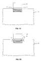
- FIG. 1is schematic cross-sectional view of a semiconductor device in accordance with the present invention.
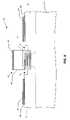
- FIG. 2is a greatly enlarged schematic cross-sectional view of the superlattice as shown in FIG. 1 .
- FIG. 3is a perspective schematic atomic diagram of a portion of the superlattice shown in FIG. 1 .
- FIG. 4is a greatly enlarged schematic cross-sectional view of another embodiment of a superlattice that may be used in the device of FIG. 1 .
- FIG. 5Ais a graph of the calculated band structure from the gamma point (G) for both bulk silicon as in the prior art, and for the 4/1 Si/O superlattice as shown in FIGS. 1-3 .
- FIG. 5Bis a graph of the calculated band structure from the Z point for both bulk silicon as in the prior art, and for the 4/1 Si/O superlattice as shown in FIGS. 1-3 .
- FIG. 5Cis a graph of the calculated band structure from both the gamma and Z points for both bulk silicon as in the prior art, and for the 5/1/3/1 Si/O superlattice as shown in FIG. 4 .
- FIGS. 6A-6Eare a series of schematic cross-sectional diagrams illustrating a method for making the semiconductor device of FIG. 1 .
- FIGS. 7A-7Eare a series of schematic cross-sectional diagrams illustrating a method for making an alternate embodiment of the semiconductor device of FIG. 1 .
- FIG. 8is a schematic cross-sectional diagram illustrating a completed semiconductor device formed using the method steps illustrated in FIGS. 7A-7E .
- the present inventionrelates to controlling the properties of semiconductor materials at the atomic or molecular level to achieve improved performance within semiconductor devices. Further, the invention relates to the identification, creation, and use of improved materials for use in the conduction paths of semiconductor devices.
- fis the Fermi-Dirac distribution
- E Fis the Fermi energy
- Tis the temperature
- E(k,n)is the energy of an electron in the state corresponding to wave vector k and the n th energy band
- the indices i and jrefer to Cartesian coordinates x, y and z
- the integralsare taken over the Brillouin zone (B.Z.)
- the summationsare taken over bands with energies above and below the Fermi energy for electrons and holes respectively.
- the conductivity reciprocal effective mass tensoris such that a tensorial component of the conductivity of the material is greater for greater values of the corresponding component of the conductivity reciprocal effective mass tensor.
- the superlattices described hereinset the values of the conductivity reciprocal effective mass tensor so as to enhance the conductive properties of the material, such as typically for a preferred direction of charge carrier transport.
- the inverse of the appropriate tensor elementis referred to as the conductivity effective mass.
- the conductivity effective mass for electrons/holes as described above and calculated in the direction of intended carrier transportis used to distinguish improved materials.
- One such examplewould be a superlattice 25 material for a channel region in a semiconductor device.
- a planar MOSFET 20 including the superlattice 25 in accordance with the inventionis now first described with reference to FIG. 1 .
- the materials identified hereincould be used in many different types of semiconductor devices, such as discrete devices and/or integrated circuits.
- the illustrated MOSFET 20includes a substrate 21 , source and drain regions 22 , 23 , and the superlattice 25 is positioned between the source and drain regions.
- the source and drain regions 22 , 23are raised source and drain regions in that they include respective epitaxial silicon layers 26 , 28 formed on the substrate 21 which are doped to the desired concentration.
- the dopantmay permeate portions 27 , 29 of the substrate 21 so that the source and drain regions 22 , 23 extend beneath the epitaxial layers 26 , 28 , respectively, and under the superlattice 25 , as shown.
- the MOSFET 20also illustratively includes a gate 35 comprising a gate insulating (e.g., oxide) layer 37 on the superlattice 25 and a gate electrode layer 36 on the gate insulating layer.
- Source/drain silicide layers 30 , 31 and source/drain contacts 32 , 33overlie the source/drain regions, as will be appreciated by those skilled in the art.
- upper portions of the superlattice 25extend above adjacent upper portions of the source and drain regions 22 , 23 , and, more particularly, the epitaxial layers 26 , 28 .
- the superlattice 25has a greater thickness than the epitaxial layers 26 , 28 , and thus upper sidewall portions of the superlattice do not contact the epitaxial layers.
- lower sidewall portions of the superlattice 25do contact the source and drain regions 22 , 23 as shown so that a channel is defined in lower portions of the superlattice.
- the channelonly occupies the lower portion of the superlattice 25 , and thus current flow is reduced in the upper portions of the superlattice near the gate insulating layer 37 .
- Thisadvantageously reduces hot carrier injection, for example, which may otherwise result in premature oxide breakdown and failure, as will be appreciated by those skilled in the art.
- Applicantshave identified improved materials or structures for the superlattice 25 of the MOSFET 20 . More specifically, the Applicants have identified materials or structures having energy band structures for which the appropriate conductivity effective masses for electrons and/or holes are substantially less than the corresponding values for silicon.
- the materials or structuresare in the form of a superlattice 25 whose structure is controlled at the atomic or molecular level and may be formed using known techniques of atomic or molecular layer deposition.
- the superlattice 25includes a plurality of layer groups 45 a - 45 n arranged in stacked relation, as perhaps best understood with specific reference to the schematic cross-sectional view of FIG. 2 .
- Each group of layers 45 a - 45 n of the superlattice 25illustratively includes a plurality of stacked base semiconductor monolayers 46 defining a respective base semiconductor portion 46 a - 46 n and an energy band-modifying layer 50 thereon.
- the energy band-modifying layers 50are indicated by stippling in FIG. 2 for clarity of illustration.
- the energy-band modifying layer 50illustratively includes one non-semiconductor monolayer constrained within a crystal lattice of adjacent base semiconductor portions. In other embodiments, more than one such monolayer may be possible. It should be noted that reference herein to a non-semiconductor or semiconductor monolayer means that the material used for the monolayer would be a non-semiconductor or semiconductor if formed in bulk. That is, a single monolayer of a material, such as semiconductor, may not necessarily exhibit the same properties that it would if formed in bulk or in a relatively thick layer, as will be appreciated by those skilled in the art.
- the energy band-modifying layers 50 and adjacent base semiconductor portions 46 a - 46 ncause the superlattice 25 to have a lower appropriate conductivity effective mass for the charge carriers in the parallel layer direction than would otherwise be present.
- this parallel directionis orthogonal to the stacking direction.
- the band modifying layers 50may also cause the superlattice 25 to have a common energy band structure.
- the semiconductor devicesuch as the illustrated MOSFET 20
- the superlattice 25may further have a substantially direct energy bandgap that may be particularly advantageous for opto-electronic devices, for example, as described in further detail below.
- the source/drain regions 22 , 23 and gate 35 of the MOSFET 20may be considered as regions for causing the transport of charge carriers through the superlattice in a parallel direction relative to the layers of the stacked groups 45 a - 45 n. Other such regions are also contemplated by the present invention.
- the superlattice 25also illustratively includes a cap layer 52 on an upper layer group 45 n
- the cap layer 52may comprise a plurality of base semiconductor monolayers 46 .
- the cap layer 52may have between 2 to 100 monolayers of the base semiconductor, and, more preferably between 10 to 50 monolayers.
- Each base semiconductor portion 46 a - 46 nmay comprise a base semiconductor selected from the group consisting of Group IV semiconductors, Group III-V semiconductors, and Group II-VI semiconductors.
- Group IV semiconductorsalso includes Group IV-IV semiconductors, as will be appreciated by those skilled in the art.
- the base semiconductormay comprise at least one of silicon and germanium, for example
- Each energy band-modifying layer 50may comprise a non-semiconductor selected from the group consisting of oxygen, nitrogen, fluorine, and carbon-oxygen for example.
- the non-semiconductoris also desirably thermally stable through deposition of a next layer to thereby facilitate manufacturing.
- the non-semiconductormay be another inorganic or organic element or compound that is compatible with the given semiconductor processing, as will be appreciated by those skilled in the art.
- the term monolayeris meant to include a single atomic layer and also a single molecular layer. It is also noted that the energy band-modifying layer 50 provided by a single monolayer is also meant to include a monolayer wherein not all of the possible sites are occupied. For example, with particular reference to the atomic diagram of FIG. 3 , a 4/1 repeating structure is illustrated for silicon as the base semiconductor material, and oxygen as the energy band-modifying material. Only half of the possible sites for oxygen are occupied.
- this one half occupationwould not necessarily be the case as will be appreciated by those skilled in the art. Indeed, it can be seen even in this schematic diagram, that individual atoms of oxygen in a given monolayer are not precisely aligned along a flat plane as will also be appreciated by those of skill in the art of atomic deposition.
- a preferred occupation rangeis from about one-eighth to one-half of the possible oxygen sites being full, although other numbers may be used in certain embodiments.
- Silicon and oxygenare currently widely used in conventional semiconductor processing, and, hence, manufacturers will be readily able to use these materials as described herein.
- Atomic or monolayer depositionis also now widely used. Accordingly, semiconductor devices incorporating the superlattice 25 in accordance with the invention may be readily adopted and implemented, as will be appreciated by those skilled in the art.
- the number of silicon monolayersshould desirably be seven or less so that the energy band of the superlattice is common or relatively uniform throughout to achieve the desired advantages.
- the 4/1 repeating structure shown in FIGS. 2 and 3 for Si/Ohas been modeled to indicate an enhanced mobility for electrons and holes in the X direction.
- the calculated conductivity effective mass for electronsis 0.26 and for the 4/1 SiO superlattice in the X direction it is 0.12, resulting in a ratio of 0.46.
- the calculation for holesyields values of 0.36 for bulk silicon and 0.16 for the 4/1 Si/O superlattice resulting in a ratio of 0.44.
- While such a directionally preferential featuremay be desired in certain semiconductor devices, other devices may benefit from a more uniform increase in mobility in any direction parallel to the groups of layers. It may also be beneficial to have an increased mobility for both electrons and holes, or just one of these types of charge carriers, as will be appreciated by those skilled in the art.
- the lower conductivity effective mass for the 4/1 Si/O embodiment of the superlattice 25may be less than two-thirds the conductivity effective mass than would otherwise occur, and this applies for both electrons and holes.
- the superlattice 25may further comprise at least one type of conductivity dopant therein as will also be appreciated by those skilled in the art.
- FIG. 4another embodiment of a superlattice 25 ′ in accordance with the invention having different properties is now described.
- a repeating pattern of 3/1/5/1is illustrated. More particularly, the lowest base semiconductor portion 46 a ′ has three monolayers, and the second lowest base semiconductor portion 46 b ′ has five monolayers. This pattern repeats throughout the superlattice 25 ′.
- the energy band-modifying layers 50 ′may each include a single monolayer.
- the enhancement of charge carrier mobilityis independent of orientation in the plane of the layers.
- all of the base semiconductor portions of a superlatticemay be a same number of monolayers thick. In other embodiments, at least some of the base semiconductor portions may be a different number of monolayers thick. In still other embodiments, all of the base semiconductor portions may be a different number of monolayers thick.
- FIGS. 5A-5Cband structures calculated using Density Functional Theory (DFT) are presented. It is well known in the art that DFT underestimates the absolute value of the bandgap. Hence all bands above the gap may be shifted by an appropriate “scissors correction.” However the shape of the band is known to be much more reliable. The vertical energy axes should be interpreted in this light.
- DFTDensity Functional Theory
- FIG. 5Ashows the calculated band structure from the gamma point (G) for both bulk silicon (represented by continuous lines) and for the 4/1 Si/O superlattice 25 as shown in FIGS. 1-3 (represented by dotted lines).
- the directionsrefer to the unit cell of the 4/1 Si/O structure and not to the conventional unit cell of Si, although the (001) direction In the figure does correspond to the (001) direction of the conventional unit cell of Si, and, hence, shows the expected location of the Si conduction band minimum.
- the (100) and (010) directions in the figurecorrespond to the (110) and ( ⁇ 110) directions of the conventional Si unit cell.
- the bands of Si on the figureare folded to represent them on the appropriate reciprocal lattice directions for the 4/1 Si/O structure.
- the conduction band minimum for the 4/1 Si/O structureis located at the gamma point in contrast to bulk silicon (Si), whereas the valence band minimum occurs at the edge of the Brillouin zone in the (001) direction which we refer to as the Z point.
- the greater curvature of the conduction band minimum for the 4/1 Si/O structurecompared to the curvature of the conduction band minimum for Si owing to the band splitting due to the perturbation introduced by the additional oxygen layer.
- FIG. 5Bshows the calculated band structure from the Z point for both bulk silicon (continuous lines) and for the 4/1 Si/O superlattice 25 (dotted lines). This figure illustrates the enhanced curvature of the valence band in the (100) direction.
- FIG. 5Cshows the calculated band structure from both the gamma and Z point for both bulk silicon (continuous lines) and for the 5/1/3/1 Si/O structure of the superlattice 25 ′ of FIG. 4 (dotted lines). Due to the symmetry of the 5/1/3/1 Si/O structure, the calculated band structures in the (100) and (010) directions are equivalent. Thus the conductivity effective mass and mobility are expected to be isotropic in the plane parallel to the layers, i.e., perpendicular to the (001) stacking direction. Note that in the 5/1/3/1 Si/O example the conduction band minimum and the valence band maximum are both at or close to the Z point.
- the appropriate comparison and discriminationmay be made via the conductivity reciprocal effective mass tensor calculation. This leads Applicants to further theorize that the 5/1/3/1 superlattice 25 ′ should be substantially direct bandgap. As will be understood by those skilled in the art, the appropriate matrix element for optical transition is another indicator of the distinction between direct and indirect bandgap behavior.
- the methodbegins with providing the silicon substrate 21 .
- the substratemay be an eight-inch wafer 21 of lightly doped P-type or N-type single crystal silicon with ⁇ 100> orientation, although other suitable substrates may also be used.
- a layer of the superlattice 25 materialis then formed across the upper surface of the substrate 21 .
- the superlattice 25 materialis deposited across the surface of the substrate 21 using atomic layer deposition and the epitaxial silicon cap layer 52 is formed, as discussed previously above, and the surface is planarized to arrive at the structure of FIG. 6A .
- the superlattice 25 materialmay be selectively deposited in those regions where channels are to be formed, rather than across the entire substrate 21 , as will be appreciated by those skilled in the art.
- planarizationmay not be required in all embodiments.
- the epitaxial silicon cap layer 52may have a preferred thickness to prevent superlattice consumption during gate oxide growth, or any other subsequent oxidations, while at the same time reducing or minimizing the thickness of the silicon cap layer to reduce any parallel path of conduction with the superlattice. According to the well-known relationship of consuming approximately 45% of the underlying silicon for a given oxide grown, the silicon cap layer may be greater than 45% of the grown gate oxide thickness plus a small incremental amount to account for manufacturing tolerances known to those skilled in the art. For the present example, and assuming growth of a 25 angstrom gate, one may use approximately 13-15 angstroms of silicon cap thickness.
- FIG. 6Bdepicts the MOSFET 20 after the gate oxide 37 and the gate electrode 36 are formed. More particularly, a thin gate oxide is deposited, and steps of poly deposition, patterning, and etching are performed, as will be appreciated by those skilled in the art.
- Poly depositionrefers to low pressure chemical vapor deposition (LPCVD) of silicon onto an oxide (hence it forms a polycrystalline material). The step includes doping with P+ or As ⁇ to make it conducting, and the layer may be around 250 nm thick, for example.
- LPCVDlow pressure chemical vapor deposition
- the pattern stepmay include performing a spinning photoresist, baking, exposure to light (i.e., a photolithography step), and developing the resist.
- the patternis then transferred to another layer (oxide or nitride) which acts as an etch mask during the etch step.
- the etch steptypically is a plasma etch (anisotropic, dry etch) that is material selective (e.g., etches silicon ten times faster than oxide) and transfers the lithography pattern into the material of interest.
- the gatemay then be used as an etch mask to remove the superlattice 25 material in the regions where the source and drain 22 , 23 are to be formed, as will be appreciated by those skilled in the art.
- the superlattice 25 materialmay be etched in a similar fashion to that described above for the gate 35 .
- the non-semiconductor present in the superlattice 25e.g., oxygen
- the superlatticemay be more easily etched using an etchant formulated for oxides rather than silicon.
- the appropriate etch for a given implementationwill vary based upon the structure and materials used for the superlattice 25 and substrate 21 , as will be appreciated by those of skill in the art.
- the epitaxial source and drain layers 26 , 28are formed, which may be done using known epitaxial deposition methods.
- the source and drain regions 22 , 23are doped using the appropriate n-type or p-type implantation. An anneal and/or clean step may be used after the implantation, but depending on the specific process, they may be omitted.
- Self-aligned silicide formationmay then be performed to form the silicide layers 30 , 31 , and 34 , and the source/drain contacts 32 , 33 , are formed to provide the final semiconductor device 20 illustrated in FIG. 1 .
- the silicide formationis also known as salicidation.
- the salicidation processincludes metal deposition (e.g. Ti), nitrogen annealing, metal etching, and a second annealing.
- the foregoingis, of course, but one example of a process and device in which the present invention may be used, and those of skill in the art will understand its application and use in many other processes and devices.
- the structures of the present inventionmay be formed on a portion of a wafer or across substantially all of a wafer.
- the use of an atomic layer deposition toolmay also not be needed for forming the superlattice 25 in some embodiments.
- the monolayersmay be formed using a CVD tool with process conditions compatible with control of monolayers, as will be appreciated by those skilled in the art.
- a trench 70 ′′is formed in the substrate 21 ′′ using known semiconductor techniques ( FIG. 7A ).
- the superlattice 25 ′′is formed within the trench 70 ′′ ( FIG. 7B ), as described above.
- the gate insulating layer 37 ′′ and gate electrode layer 36 ′′are then formed and patterned, as necessary, as seen in FIG. 7C .
- Trenches 71 ′′, 72 ′′are then formed next to the gate in the substrate 21 ′′ in the areas where the source and drain regions 23 ′′, 24 ′′ are to be formed ( FIG. 7D ).
- the upper portions of the superlattice 25 ′′extend above bottom portions 73 ′′, 74 ′′ of the trenches 71 ′′, 72 ′′. Again, this creates a channel region which occupies only the lower portions of the superlattice 25 ′′, thus advantageously reducing current flow near the gate insulation layer 37 ′′.
- Source and drain implantationis next performed, as described above, to form the source and drain regions 22 ′′, 23 ′′ ( FIG. 7E ).
- silicide formationmay then be performed to form the silicide layers 30 ′′, 31 ′′, and 34 ′′, and the source/drain contacts 32 ′′, 33 ′′ are formed to provide the final semiconductor device 20 ′′ illustrated in FIG. 8 .
- the trenches 71 ′′, 72 ′′may be formed after implantation of the source and drain regions 22 ′′, 23 ′′.
- the trenches 71 ′′, 72 ′′may be formed in the superlattice 25 ′′ at the outer edges thereof to provide the desired separation between the upper portions of the superlattice and the source and drain regions 22 ′′, 23 ′′, as will be appreciated by those skilled in the art.
- MOSFET 20 ′′While only a single MOSFET 20 ′′ has been illustrated in the drawings and described above for clarity of explanation and illustration, it will be appreciated that multiple MOSFETs may be formed in the substrate 21 ′′, such as NMOS and PMOS transistors to provide a CMOS device. More particularly, shallow trench isolation (STI) regions (not shown) may be formed between adjacent MOSFETS, as will be appreciated by those skilled in the art. In accordance with one embodiment, the STI regions may be formed prior to depositing the superlattice 25 ′′, so that the STI regions thus provide boundaries for selective deposition of the superlattice.
- STIshallow trench isolation
- the waferis patterned and trenches are etched (e.g., 0.3-0.8 um) in the desired STI regions.
- a thin oxideis then grown, and the trenches are filled with Si0 2 to provide the STI regions, and the upper surfaces thereof may be planarized, if desired.
- the STI regionsmay also be used as an etch stop in performing certain of the above-noted steps, as will be appreciated by those skilled in the art.
- the superlattice 25 ′′ structuremay also be formed prior to formation of the STI regions to thereby eliminate a masking step, if desired. Further details regarding fabrication of the semiconductor devices in accordance with the present invention may be found in the above-noted U.S. application Ser. No. 10/467,069.
Landscapes
- Insulated Gate Type Field-Effect Transistor (AREA)
- Light Receiving Elements (AREA)
- Metal-Oxide And Bipolar Metal-Oxide Semiconductor Integrated Circuits (AREA)
Abstract
Description
for electrons and:
for holes, where f is the Fermi-Dirac distribution, EFis the Fermi energy, T is the temperature, E(k,n) is the energy of an electron in the state corresponding to wave vector k and the nthenergy band, the indices i and j refer to Cartesian coordinates x, y and z, the integrals are taken over the Brillouin zone (B.Z.), and the summations are taken over bands with energies above and below the Fermi energy for electrons and holes respectively.
Claims (46)
Priority Applications (11)
| Application Number | Priority Date | Filing Date | Title |
|---|---|---|---|
| US10/941,062US7279701B2 (en) | 2003-06-26 | 2004-09-14 | Semiconductor device comprising a superlattice with upper portions extending above adjacent upper portions of source and drain regions |
| US11/457,256US7612366B2 (en) | 2003-06-26 | 2006-07-13 | Semiconductor device including a strained superlattice layer above a stress layer |
| US11/457,293US20070020860A1 (en) | 2003-06-26 | 2006-07-13 | Method for Making Semiconductor Device Including a Strained Superlattice and Overlying Stress Layer and Related Methods |
| US11/457,299US20070012910A1 (en) | 2003-06-26 | 2006-07-13 | Semiconductor Device Including a Channel with a Non-Semiconductor Layer Monolayer |
| US11/457,269US7531828B2 (en) | 2003-06-26 | 2006-07-13 | Semiconductor device including a strained superlattice between at least one pair of spaced apart stress regions |
| US11/457,263US20070010040A1 (en) | 2003-06-26 | 2006-07-13 | Method for Making a Semiconductor Device Including a Strained Superlattice Layer Above a Stress Layer |
| US11/457,315US20070020833A1 (en) | 2003-06-26 | 2006-07-13 | Method for Making a Semiconductor Device Including a Channel with a Non-Semiconductor Layer Monolayer |
| US11/457,286US7598515B2 (en) | 2003-06-26 | 2006-07-13 | Semiconductor device including a strained superlattice and overlying stress layer and related methods |
| US11/457,276US20070015344A1 (en) | 2003-06-26 | 2006-07-13 | Method for Making a Semiconductor Device Including a Strained Superlattice Between at Least One Pair of Spaced Apart Stress Regions |
| US11/534,796US20070063185A1 (en) | 2003-06-26 | 2006-09-25 | Semiconductor device including a front side strained superlattice layer and a back side stress layer |
| US11/534,819US20070063186A1 (en) | 2003-06-26 | 2006-09-25 | Method for making a semiconductor device including a front side strained superlattice layer and a back side stress layer |
Applications Claiming Priority (4)
| Application Number | Priority Date | Filing Date | Title |
|---|---|---|---|
| US10/603,696US20040262594A1 (en) | 2003-06-26 | 2003-06-26 | Semiconductor structures having improved conductivity effective mass and methods for fabricating same |
| US10/603,621US20040266116A1 (en) | 2003-06-26 | 2003-06-26 | Methods of fabricating semiconductor structures having improved conductivity effective mass |
| US10/647,069US6897472B2 (en) | 2003-06-26 | 2003-08-22 | Semiconductor device including MOSFET having band-engineered superlattice |
| US10/941,062US7279701B2 (en) | 2003-06-26 | 2004-09-14 | Semiconductor device comprising a superlattice with upper portions extending above adjacent upper portions of source and drain regions |
Related Parent Applications (2)
| Application Number | Title | Priority Date | Filing Date |
|---|---|---|---|
| US10/647,069Continuation-In-PartUS6897472B2 (en) | 2003-06-26 | 2003-08-22 | Semiconductor device including MOSFET having band-engineered superlattice |
| US10/940,594Continuation-In-PartUS7288457B2 (en) | 2003-06-26 | 2004-09-14 | Method for making semiconductor device comprising a superlattice with upper portions extending above adjacent upper portions of source and drain regions |
Related Child Applications (9)
| Application Number | Title | Priority Date | Filing Date |
|---|---|---|---|
| US11/042,270Continuation-In-PartUS7435988B2 (en) | 2003-06-26 | 2005-01-25 | Semiconductor device including a MOSFET having a band-engineered superlattice with a semiconductor cap layer providing a channel |
| US11/457,263Continuation-In-PartUS20070010040A1 (en) | 2003-06-26 | 2006-07-13 | Method for Making a Semiconductor Device Including a Strained Superlattice Layer Above a Stress Layer |
| US11/457,286Continuation-In-PartUS7598515B2 (en) | 2003-06-26 | 2006-07-13 | Semiconductor device including a strained superlattice and overlying stress layer and related methods |
| US11/457,293Continuation-In-PartUS20070020860A1 (en) | 2003-06-26 | 2006-07-13 | Method for Making Semiconductor Device Including a Strained Superlattice and Overlying Stress Layer and Related Methods |
| US11/457,256Continuation-In-PartUS7612366B2 (en) | 2003-06-26 | 2006-07-13 | Semiconductor device including a strained superlattice layer above a stress layer |
| US11/457,276Continuation-In-PartUS20070015344A1 (en) | 2003-06-26 | 2006-07-13 | Method for Making a Semiconductor Device Including a Strained Superlattice Between at Least One Pair of Spaced Apart Stress Regions |
| US11/457,269Continuation-In-PartUS7531828B2 (en) | 2003-06-26 | 2006-07-13 | Semiconductor device including a strained superlattice between at least one pair of spaced apart stress regions |
| US11/457,299Continuation-In-PartUS20070012910A1 (en) | 2003-06-26 | 2006-07-13 | Semiconductor Device Including a Channel with a Non-Semiconductor Layer Monolayer |
| US11/457,315Continuation-In-PartUS20070020833A1 (en) | 2003-06-26 | 2006-07-13 | Method for Making a Semiconductor Device Including a Channel with a Non-Semiconductor Layer Monolayer |
Publications (2)
| Publication Number | Publication Date |
|---|---|
| US20050110003A1 US20050110003A1 (en) | 2005-05-26 |
| US7279701B2true US7279701B2 (en) | 2007-10-09 |
Family
ID=34119859
Family Applications (13)
| Application Number | Title | Priority Date | Filing Date |
|---|---|---|---|
| US10/936,913Expired - LifetimeUS7446334B2 (en) | 2003-06-26 | 2004-09-09 | Electronic device comprising active optical devices with an energy band engineered superlattice |
| US10/936,920Expired - LifetimeUS7109052B2 (en) | 2003-06-26 | 2004-09-09 | Method for making an integrated circuit comprising a waveguide having an energy band engineered superlattice |
| US10/937,072AbandonedUS20050029510A1 (en) | 2003-06-26 | 2004-09-09 | Method for making electronic device comprising active optical devices with an energy band engineered superlattice |
| US10/936,933AbandonedUS20050032247A1 (en) | 2003-06-26 | 2004-09-09 | Method for making an integrated circuit comprising an active optical device having an energy band engineered superlattice |
| US10/936,903Expired - LifetimeUS7432524B2 (en) | 2003-06-26 | 2004-09-09 | Integrated circuit comprising an active optical device having an energy band engineered superlattice |
| US10/937,071Expired - LifetimeUS7279699B2 (en) | 2003-06-26 | 2004-09-09 | Integrated circuit comprising a waveguide having an energy band engineered superlattice |
| US10/940,594Expired - LifetimeUS7288457B2 (en) | 2003-06-26 | 2004-09-14 | Method for making semiconductor device comprising a superlattice with upper portions extending above adjacent upper portions of source and drain regions |
| US10/940,426Expired - LifetimeUS7436026B2 (en) | 2003-06-26 | 2004-09-14 | Semiconductor device comprising a superlattice channel vertically stepped above source and drain regions |
| US10/940,418Expired - LifetimeUS7018900B2 (en) | 2003-06-26 | 2004-09-14 | Method for making a semiconductor device comprising a superlattice channel vertically stepped above source and drain regions |
| US10/941,062Expired - LifetimeUS7279701B2 (en) | 2003-06-26 | 2004-09-14 | Semiconductor device comprising a superlattice with upper portions extending above adjacent upper portions of source and drain regions |
| US11/042,270Expired - LifetimeUS7435988B2 (en) | 2003-06-26 | 2005-01-25 | Semiconductor device including a MOSFET having a band-engineered superlattice with a semiconductor cap layer providing a channel |
| US11/042,272Expired - LifetimeUS7265002B2 (en) | 2003-06-26 | 2005-01-25 | Method for making a semiconductor device including a MOSFET having a band-engineered superlattice with a semiconductor cap layer providing a channel |
| US11/089,950Expired - LifetimeUS7303948B2 (en) | 2003-06-26 | 2005-03-25 | Semiconductor device including MOSFET having band-engineered superlattice |
Family Applications Before (9)
| Application Number | Title | Priority Date | Filing Date |
|---|---|---|---|
| US10/936,913Expired - LifetimeUS7446334B2 (en) | 2003-06-26 | 2004-09-09 | Electronic device comprising active optical devices with an energy band engineered superlattice |
| US10/936,920Expired - LifetimeUS7109052B2 (en) | 2003-06-26 | 2004-09-09 | Method for making an integrated circuit comprising a waveguide having an energy band engineered superlattice |
| US10/937,072AbandonedUS20050029510A1 (en) | 2003-06-26 | 2004-09-09 | Method for making electronic device comprising active optical devices with an energy band engineered superlattice |
| US10/936,933AbandonedUS20050032247A1 (en) | 2003-06-26 | 2004-09-09 | Method for making an integrated circuit comprising an active optical device having an energy band engineered superlattice |
| US10/936,903Expired - LifetimeUS7432524B2 (en) | 2003-06-26 | 2004-09-09 | Integrated circuit comprising an active optical device having an energy band engineered superlattice |
| US10/937,071Expired - LifetimeUS7279699B2 (en) | 2003-06-26 | 2004-09-09 | Integrated circuit comprising a waveguide having an energy band engineered superlattice |
| US10/940,594Expired - LifetimeUS7288457B2 (en) | 2003-06-26 | 2004-09-14 | Method for making semiconductor device comprising a superlattice with upper portions extending above adjacent upper portions of source and drain regions |
| US10/940,426Expired - LifetimeUS7436026B2 (en) | 2003-06-26 | 2004-09-14 | Semiconductor device comprising a superlattice channel vertically stepped above source and drain regions |
| US10/940,418Expired - LifetimeUS7018900B2 (en) | 2003-06-26 | 2004-09-14 | Method for making a semiconductor device comprising a superlattice channel vertically stepped above source and drain regions |
Family Applications After (3)
| Application Number | Title | Priority Date | Filing Date |
|---|---|---|---|
| US11/042,270Expired - LifetimeUS7435988B2 (en) | 2003-06-26 | 2005-01-25 | Semiconductor device including a MOSFET having a band-engineered superlattice with a semiconductor cap layer providing a channel |
| US11/042,272Expired - LifetimeUS7265002B2 (en) | 2003-06-26 | 2005-01-25 | Method for making a semiconductor device including a MOSFET having a band-engineered superlattice with a semiconductor cap layer providing a channel |
| US11/089,950Expired - LifetimeUS7303948B2 (en) | 2003-06-26 | 2005-03-25 | Semiconductor device including MOSFET having band-engineered superlattice |
Country Status (6)
| Country | Link |
|---|---|
| US (13) | US7446334B2 (en) |
| EP (1) | EP1644983B1 (en) |
| JP (1) | JP2007521648A (en) |
| AU (1) | AU2004300982B2 (en) |
| CA (1) | CA2530065C (en) |
| WO (1) | WO2005018005A1 (en) |
Cited By (78)
| Publication number | Priority date | Publication date | Assignee | Title |
|---|---|---|---|---|
| US20070012912A1 (en)* | 2003-06-26 | 2007-01-18 | Rj Mears, Llc | Semiconductor Device Including a Strained Superlattice and Overlying Stress Layer and Related Methods |
| US20100296540A1 (en)* | 2009-05-22 | 2010-11-25 | James Pan | Resonant Cavity Complementary Optoelectronic Transistors |
| US9275996B2 (en) | 2013-11-22 | 2016-03-01 | Mears Technologies, Inc. | Vertical semiconductor devices including superlattice punch through stop layer and related methods |
| US9406753B2 (en) | 2013-11-22 | 2016-08-02 | Atomera Incorporated | Semiconductor devices including superlattice depletion layer stack and related methods |
| US9558939B1 (en) | 2016-01-15 | 2017-01-31 | Atomera Incorporated | Methods for making a semiconductor device including atomic layer structures using N2O as an oxygen source |
| US9716147B2 (en) | 2014-06-09 | 2017-07-25 | Atomera Incorporated | Semiconductor devices with enhanced deterministic doping and related methods |
| US9722046B2 (en) | 2014-11-25 | 2017-08-01 | Atomera Incorporated | Semiconductor device including a superlattice and replacement metal gate structure and related methods |
| US9721790B2 (en) | 2015-06-02 | 2017-08-01 | Atomera Incorporated | Method for making enhanced semiconductor structures in single wafer processing chamber with desired uniformity control |
| US9899479B2 (en) | 2015-05-15 | 2018-02-20 | Atomera Incorporated | Semiconductor devices with superlattice layers providing halo implant peak confinement and related methods |
| US10107854B2 (en) | 2016-08-17 | 2018-10-23 | Atomera Incorporated | Semiconductor device including threshold voltage measurement circuitry |
| US10109479B1 (en) | 2017-07-31 | 2018-10-23 | Atomera Incorporated | Method of making a semiconductor device with a buried insulating layer formed by annealing a superlattice |
| US10109342B2 (en) | 2016-05-11 | 2018-10-23 | Atomera Incorporated | Dram architecture to reduce row activation circuitry power and peripheral leakage and related methods |
| US10170603B2 (en) | 2016-08-08 | 2019-01-01 | Atomera Incorporated | Semiconductor device including a resonant tunneling diode structure with electron mean free path control layers |
| US10276625B1 (en) | 2017-12-15 | 2019-04-30 | Atomera Incorporated | CMOS image sensor including superlattice to enhance infrared light absorption |
| US10304881B1 (en) | 2017-12-15 | 2019-05-28 | Atomera Incorporated | CMOS image sensor with buried superlattice layer to reduce crosstalk |
| US10355151B2 (en) | 2017-12-15 | 2019-07-16 | Atomera Incorporated | CMOS image sensor including photodiodes with overlying superlattices to reduce crosstalk |
| US10361243B2 (en) | 2017-12-15 | 2019-07-23 | Atomera Incorporated | Method for making CMOS image sensor including superlattice to enhance infrared light absorption |
| US10367064B2 (en) | 2017-06-13 | 2019-07-30 | Atomera Incorporated | Semiconductor device with recessed channel array transistor (RCAT) including a superlattice |
| US10367028B2 (en) | 2017-12-15 | 2019-07-30 | Atomera Incorporated | CMOS image sensor including stacked semiconductor chips and image processing circuitry including a superlattice |
| US10381242B2 (en) | 2017-05-16 | 2019-08-13 | Atomera Incorporated | Method for making a semiconductor device including a superlattice as a gettering layer |
| US10396223B2 (en) | 2017-12-15 | 2019-08-27 | Atomera Incorporated | Method for making CMOS image sensor with buried superlattice layer to reduce crosstalk |
| US10461118B2 (en) | 2017-12-15 | 2019-10-29 | Atomera Incorporated | Method for making CMOS image sensor including photodiodes with overlying superlattices to reduce crosstalk |
| US10468245B2 (en) | 2018-03-09 | 2019-11-05 | Atomera Incorporated | Semiconductor device including compound semiconductor materials and an impurity and point defect blocking superlattice |
| US10529757B2 (en) | 2017-12-15 | 2020-01-07 | Atomera Incorporated | CMOS image sensor including pixels with read circuitry having a superlattice |
| US10529768B2 (en) | 2017-12-15 | 2020-01-07 | Atomera Incorporated | Method for making CMOS image sensor including pixels with read circuitry having a superlattice |
| US10566191B1 (en) | 2018-08-30 | 2020-02-18 | Atomera Incorporated | Semiconductor device including superlattice structures with reduced defect densities |
| US10580867B1 (en) | 2018-11-16 | 2020-03-03 | Atomera Incorporated | FINFET including source and drain regions with dopant diffusion blocking superlattice layers to reduce contact resistance |
| US10580866B1 (en) | 2018-11-16 | 2020-03-03 | Atomera Incorporated | Semiconductor device including source/drain dopant diffusion blocking superlattices to reduce contact resistance |
| US10593761B1 (en) | 2018-11-16 | 2020-03-17 | Atomera Incorporated | Method for making a semiconductor device having reduced contact resistance |
| US10608043B2 (en) | 2017-12-15 | 2020-03-31 | Atomera Incorporation | Method for making CMOS image sensor including stacked semiconductor chips and readout circuitry including a superlattice |
| US10608027B2 (en) | 2017-12-15 | 2020-03-31 | Atomera Incorporated | Method for making CMOS image sensor including stacked semiconductor chips and image processing circuitry including a superlattice |
| US10615209B2 (en) | 2017-12-15 | 2020-04-07 | Atomera Incorporated | CMOS image sensor including stacked semiconductor chips and readout circuitry including a superlattice |
| US10727049B2 (en) | 2018-03-09 | 2020-07-28 | Atomera Incorporated | Method for making a semiconductor device including compound semiconductor materials and an impurity and point defect blocking superlattice |
| US10741436B2 (en) | 2017-08-18 | 2020-08-11 | Atomera Incorporated | Method for making a semiconductor device including non-monocrystalline stringer adjacent a superlattice-sti interface |
| US10763370B2 (en) | 2018-04-12 | 2020-09-01 | Atomera Incorporated | Inverted T channel field effect transistor (ITFET) including a superlattice |
| US10777451B2 (en) | 2018-03-08 | 2020-09-15 | Atomera Incorporated | Semiconductor device including enhanced contact structures having a superlattice |
| US10811498B2 (en) | 2018-08-30 | 2020-10-20 | Atomera Incorporated | Method for making superlattice structures with reduced defect densities |
| US10818755B2 (en) | 2018-11-16 | 2020-10-27 | Atomera Incorporated | Method for making semiconductor device including source/drain dopant diffusion blocking superlattices to reduce contact resistance |
| US10825902B1 (en) | 2019-07-17 | 2020-11-03 | Atomera Incorporated | Varactor with hyper-abrupt junction region including spaced-apart superlattices |
| US10825901B1 (en) | 2019-07-17 | 2020-11-03 | Atomera Incorporated | Semiconductor devices including hyper-abrupt junction region including a superlattice |
| US10840335B2 (en) | 2018-11-16 | 2020-11-17 | Atomera Incorporated | Method for making semiconductor device including body contact dopant diffusion blocking superlattice to reduce contact resistance |
| US10840336B2 (en) | 2018-11-16 | 2020-11-17 | Atomera Incorporated | Semiconductor device with metal-semiconductor contacts including oxygen insertion layer to constrain dopants and related methods |
| US10840337B2 (en) | 2018-11-16 | 2020-11-17 | Atomera Incorporated | Method for making a FINFET having reduced contact resistance |
| US10840388B1 (en) | 2019-07-17 | 2020-11-17 | Atomera Incorporated | Varactor with hyper-abrupt junction region including a superlattice |
| US10847618B2 (en) | 2018-11-16 | 2020-11-24 | Atomera Incorporated | Semiconductor device including body contact dopant diffusion blocking superlattice having reduced contact resistance |
| US10854717B2 (en) | 2018-11-16 | 2020-12-01 | Atomera Incorporated | Method for making a FINFET including source and drain dopant diffusion blocking superlattices to reduce contact resistance |
| US10868120B1 (en) | 2019-07-17 | 2020-12-15 | Atomera Incorporated | Method for making a varactor with hyper-abrupt junction region including a superlattice |
| US10879357B1 (en) | 2019-07-17 | 2020-12-29 | Atomera Incorporated | Method for making a semiconductor device having a hyper-abrupt junction region including a superlattice |
| US10884185B2 (en) | 2018-04-12 | 2021-01-05 | Atomera Incorporated | Semiconductor device including vertically integrated optical and electronic devices and comprising a superlattice |
| US10916642B2 (en) | 2019-04-18 | 2021-02-09 | Globalfoundries U.S. Inc. | Heterojunction bipolar transistor with emitter base junction oxide interface |
| US10937868B2 (en) | 2019-07-17 | 2021-03-02 | Atomera Incorporated | Method for making semiconductor devices with hyper-abrupt junction region including spaced-apart superlattices |
| US10937888B2 (en) | 2019-07-17 | 2021-03-02 | Atomera Incorporated | Method for making a varactor with a hyper-abrupt junction region including spaced-apart superlattices |
| US11075078B1 (en) | 2020-03-06 | 2021-07-27 | Atomera Incorporated | Method for making a semiconductor device including a superlattice within a recessed etch |
| US11094818B2 (en) | 2019-04-23 | 2021-08-17 | Atomera Incorporated | Method for making a semiconductor device including a superlattice and an asymmetric channel and related methods |
| US11158722B2 (en) | 2019-12-30 | 2021-10-26 | Globalfoundries U.S. Inc. | Transistors with lattice structure |
| US11177351B2 (en) | 2020-02-26 | 2021-11-16 | Atomera Incorporated | Semiconductor device including a superlattice with different non-semiconductor material monolayers |
| US11183565B2 (en) | 2019-07-17 | 2021-11-23 | Atomera Incorporated | Semiconductor devices including hyper-abrupt junction region including spaced-apart superlattices and related methods |
| US11264499B2 (en) | 2019-09-16 | 2022-03-01 | Globalfoundries U.S. Inc. | Transistor devices with source/drain regions comprising an interface layer that comprises a non-semiconductor material |
| US11302823B2 (en) | 2020-02-26 | 2022-04-12 | Atomera Incorporated | Method for making semiconductor device including a superlattice with different non-semiconductor material monolayers |
| US11437486B2 (en) | 2020-01-14 | 2022-09-06 | Atomera Incorporated | Methods for making bipolar junction transistors including emitter-base and base-collector superlattices |
| US11469302B2 (en) | 2020-06-11 | 2022-10-11 | Atomera Incorporated | Semiconductor device including a superlattice and providing reduced gate leakage |
| US11569368B2 (en) | 2020-06-11 | 2023-01-31 | Atomera Incorporated | Method for making semiconductor device including a superlattice and providing reduced gate leakage |
| US11631584B1 (en) | 2021-10-28 | 2023-04-18 | Atomera Incorporated | Method for making semiconductor device with selective etching of superlattice to define etch stop layer |
| US11682712B2 (en) | 2021-05-26 | 2023-06-20 | Atomera Incorporated | Method for making semiconductor device including superlattice with O18 enriched monolayers |
| US11721546B2 (en) | 2021-10-28 | 2023-08-08 | Atomera Incorporated | Method for making semiconductor device with selective etching of superlattice to accumulate non-semiconductor atoms |
| US11728385B2 (en) | 2021-05-26 | 2023-08-15 | Atomera Incorporated | Semiconductor device including superlattice with O18 enriched monolayers |
| US11742202B2 (en) | 2021-03-03 | 2023-08-29 | Atomera Incorporated | Methods for making radio frequency (RF) semiconductor devices including a ground plane layer having a superlattice |
| US11810784B2 (en) | 2021-04-21 | 2023-11-07 | Atomera Incorporated | Method for making semiconductor device including a superlattice and enriched silicon 28 epitaxial layer |
| US11837634B2 (en) | 2020-07-02 | 2023-12-05 | Atomera Incorporated | Semiconductor device including superlattice with oxygen and carbon monolayers |
| US11862717B2 (en) | 2021-08-24 | 2024-01-02 | Globalfoundries U.S. Inc. | Lateral bipolar transistor structure with superlattice layer and method to form same |
| US11923418B2 (en) | 2021-04-21 | 2024-03-05 | Atomera Incorporated | Semiconductor device including a superlattice and enriched silicon 28 epitaxial layer |
| US12142669B2 (en) | 2023-03-24 | 2024-11-12 | Atomera Incorporated | Method for making nanostructure transistors with flush source/drain dopant blocking structures including a superlattice |
| US12191160B2 (en) | 2020-07-02 | 2025-01-07 | Atomera Incorporated | Method for making a semiconductor superlattices with different non-semiconductor thermal stabilities |
| US12267996B2 (en) | 2022-05-04 | 2025-04-01 | Atomera Incorporated | DRAM sense amplifier architecture with reduced power consumption and related methods |
| US12308229B2 (en) | 2023-07-03 | 2025-05-20 | Atomera Incorporated | Method for making memory device including a superlattice gettering layer |
| US12315722B2 (en) | 2023-03-14 | 2025-05-27 | Atomera Incorporated | Method for making a radio frequency silicon-on-insulator (RFSOI) wafer including a superlattice |
| US12382689B2 (en) | 2023-05-08 | 2025-08-05 | Atomera Incorporated | Method for making DMOS devices including a superlattice and field plate for drift region diffusion |
| US12439658B2 (en) | 2021-05-18 | 2025-10-07 | Atomera Incorporated | Semiconductor device including a superlattice providing metal work function tuning |
Families Citing this family (53)
| Publication number | Priority date | Publication date | Assignee | Title |
|---|---|---|---|---|
| US20070015344A1 (en)* | 2003-06-26 | 2007-01-18 | Rj Mears, Llc | Method for Making a Semiconductor Device Including a Strained Superlattice Between at Least One Pair of Spaced Apart Stress Regions |
| US20070010040A1 (en)* | 2003-06-26 | 2007-01-11 | Rj Mears, Llc | Method for Making a Semiconductor Device Including a Strained Superlattice Layer Above a Stress Layer |
| US7227174B2 (en) | 2003-06-26 | 2007-06-05 | Rj Mears, Llc | Semiconductor device including a superlattice and adjacent semiconductor layer with doped regions defining a semiconductor junction |
| US7531828B2 (en)* | 2003-06-26 | 2009-05-12 | Mears Technologies, Inc. | Semiconductor device including a strained superlattice between at least one pair of spaced apart stress regions |
| US20070020860A1 (en)* | 2003-06-26 | 2007-01-25 | Rj Mears, Llc | Method for Making Semiconductor Device Including a Strained Superlattice and Overlying Stress Layer and Related Methods |
| US6878576B1 (en)* | 2003-06-26 | 2005-04-12 | Rj Mears, Llc | Method for making semiconductor device including band-engineered superlattice |
| US20060289049A1 (en)* | 2003-06-26 | 2006-12-28 | Rj Mears, Llc | Semiconductor Device Having a Semiconductor-on-Insulator (SOI) Configuration and Including a Superlattice on a Thin Semiconductor Layer |
| US20070063185A1 (en)* | 2003-06-26 | 2007-03-22 | Rj Mears, Llc | Semiconductor device including a front side strained superlattice layer and a back side stress layer |
| US7229902B2 (en)* | 2003-06-26 | 2007-06-12 | Rj Mears, Llc | Method for making a semiconductor device including a superlattice with regions defining a semiconductor junction |
| US20050279991A1 (en)* | 2003-06-26 | 2005-12-22 | Rj Mears, Llc | Semiconductor device including a superlattice having at least one group of substantially undoped layers |
| US20060011905A1 (en)* | 2003-06-26 | 2006-01-19 | Rj Mears, Llc | Semiconductor device comprising a superlattice dielectric interface layer |
| JP2007521648A (en)* | 2003-06-26 | 2007-08-02 | アール.ジェイ. メアーズ エルエルシー | Semiconductor device having MOSFET with band design superlattice |
| US20070020833A1 (en)* | 2003-06-26 | 2007-01-25 | Rj Mears, Llc | Method for Making a Semiconductor Device Including a Channel with a Non-Semiconductor Layer Monolayer |
| US7045813B2 (en)* | 2003-06-26 | 2006-05-16 | Rj Mears, Llc | Semiconductor device including a superlattice with regions defining a semiconductor junction |
| US7535041B2 (en)* | 2003-06-26 | 2009-05-19 | Mears Technologies, Inc. | Method for making a semiconductor device including regions of band-engineered semiconductor superlattice to reduce device-on resistance |
| US7153763B2 (en)* | 2003-06-26 | 2006-12-26 | Rj Mears, Llc | Method for making a semiconductor device including band-engineered superlattice using intermediate annealing |
| US7491587B2 (en)* | 2003-06-26 | 2009-02-17 | Mears Technologies, Inc. | Method for making a semiconductor device having a semiconductor-on-insulator (SOI) configuration and including a superlattice on a thin semiconductor layer |
| US7514328B2 (en) | 2003-06-26 | 2009-04-07 | Mears Technologies, Inc. | Method for making a semiconductor device including shallow trench isolation (STI) regions with a superlattice therebetween |
| US7612366B2 (en)* | 2003-06-26 | 2009-11-03 | Mears Technologies, Inc. | Semiconductor device including a strained superlattice layer above a stress layer |
| US7586116B2 (en) | 2003-06-26 | 2009-09-08 | Mears Technologies, Inc. | Semiconductor device having a semiconductor-on-insulator configuration and a superlattice |
| US20050282330A1 (en)* | 2003-06-26 | 2005-12-22 | Rj Mears, Llc | Method for making a semiconductor device including a superlattice having at least one group of substantially undoped layers |
| US7531829B2 (en)* | 2003-06-26 | 2009-05-12 | Mears Technologies, Inc. | Semiconductor device including regions of band-engineered semiconductor superlattice to reduce device-on resistance |
| JP4059183B2 (en)* | 2003-10-07 | 2008-03-12 | ソニー株式会社 | Insulator thin film manufacturing method |
| WO2006077585A2 (en)* | 2005-01-18 | 2006-07-27 | Shye Shapira | Apparatus and method for control of tunneling in a small-scale electronic structure |
| US7465972B2 (en)* | 2005-01-21 | 2008-12-16 | Taiwan Semiconductor Manufacturing Company, Ltd. | High performance CMOS device design |
| US20060202269A1 (en) | 2005-03-08 | 2006-09-14 | Semiconductor Energy Laboratory Co., Ltd. | Wireless chip and electronic appliance having the same |
| JP2009529780A (en)* | 2005-06-20 | 2009-08-20 | メアーズ テクノロジーズ, インコーポレイテッド | Semiconductor device including a shallow trench isolation (STI) region having a superlattice therebetween, and a method for manufacturing the same |
| EP1920466A1 (en)* | 2005-06-30 | 2008-05-14 | Mears Technologies, Inc. | Semiconductor device having a semiconductor-on-insulator (soi) configuration and including a superlattice on a thin semiconductor layer and associated methods |
| US7166485B1 (en)* | 2005-07-05 | 2007-01-23 | Sharp Laboratories Of America, Inc. | Superlattice nanocrystal Si-SiO2 electroluminescence device |
| WO2007011628A1 (en)* | 2005-07-15 | 2007-01-25 | Mears Technologies, Inc. | Semiconductor device including a strained superlattice and overlying stress layer and related methods |
| US7608515B2 (en)* | 2006-02-14 | 2009-10-27 | Taiwan Semiconductor Manufacturing Company, Ltd. | Diffusion layer for stressed semiconductor devices |
| US7323392B2 (en)* | 2006-03-28 | 2008-01-29 | Taiwan Semiconductor Manufacturing Company, Ltd. | High performance transistor with a highly stressed channel |
| JP2009536464A (en)* | 2006-05-05 | 2009-10-08 | メアーズ テクノロジーズ, インコーポレイテッド | Semiconductor device having superlattice arrangement with semiconductor present on insulator and related method |
| EP2016624A1 (en)* | 2006-05-05 | 2009-01-21 | Mears Technologies, Inc. | Semiconductor device including a floating gate memory cell with a superlattice channel and associated methods |
| US20080070356A1 (en)* | 2006-09-14 | 2008-03-20 | Advanced Micro Devices, Inc. | Trench replacement gate process for transistors having elevated source and drain regions |
| US7781827B2 (en)* | 2007-01-24 | 2010-08-24 | Mears Technologies, Inc. | Semiconductor device with a vertical MOSFET including a superlattice and related methods |
| US7880161B2 (en)* | 2007-02-16 | 2011-02-01 | Mears Technologies, Inc. | Multiple-wavelength opto-electronic device including a superlattice |
| US7863066B2 (en)* | 2007-02-16 | 2011-01-04 | Mears Technologies, Inc. | Method for making a multiple-wavelength opto-electronic device including a superlattice |
| GB0717976D0 (en)* | 2007-09-14 | 2007-10-31 | Tavkhelldze Avto | Quantum interference depression effect MOS transistor |
| US7704844B2 (en)* | 2007-10-04 | 2010-04-27 | International Business Machines Corporation | High performance MOSFET |
| MX338098B (en)* | 2009-03-09 | 2016-04-01 | Bioatla Llc | Mirac proteins. |
| TWI419324B (en)* | 2009-11-27 | 2013-12-11 | Univ Nat Chiao Tung | Semiconductor device having three-five-group channel and four-group source drain and manufacturing method thereof |
| US8203155B2 (en)* | 2009-12-01 | 2012-06-19 | Massachusetts Institute Of Technology | Cavity-enhanced multispectral photonic devices |
| EA027502B1 (en) | 2009-12-23 | 2017-08-31 | Зиниммуне Гмбх | Anti-flt3 antibodies and methods of using the same |
| CN101819996B (en)* | 2010-04-16 | 2011-10-26 | 清华大学 | Semiconductor structure |
| JP5605182B2 (en)* | 2010-11-17 | 2014-10-15 | 富士通セミコンダクター株式会社 | Semiconductor device manufacturing method and semiconductor device |
| KR101467237B1 (en)* | 2013-07-01 | 2014-12-01 | 성균관대학교산학협력단 | Semiconductor device having superlattice-structured thin film laminated by semiconducting thin film and insulating thin film |
| JP6702268B2 (en) | 2017-06-15 | 2020-05-27 | 信越半導体株式会社 | Epitaxial wafer manufacturing method |
| TWI720587B (en)* | 2018-08-30 | 2021-03-01 | 美商安托梅拉公司 | Method and device for making superlattice structures with reduced defect densities |
| US20200135489A1 (en)* | 2018-10-31 | 2020-04-30 | Atomera Incorporated | Method for making a semiconductor device including a superlattice having nitrogen diffused therein |
| JP7247902B2 (en) | 2020-01-10 | 2023-03-29 | 信越半導体株式会社 | Epitaxial wafer manufacturing method |
| CN116685723A (en) | 2021-01-25 | 2023-09-01 | 信越半导体株式会社 | Method for manufacturing epitaxial wafer |
| CN113539792B (en)* | 2021-07-09 | 2024-03-01 | 中国科学院上海微系统与信息技术研究所 | Preparation method of full-surrounding grid transistor |
Citations (39)
| Publication number | Priority date | Publication date | Assignee | Title |
|---|---|---|---|---|
| US4485128A (en) | 1981-11-20 | 1984-11-27 | Chronar Corporation | Bandgap control in amorphous semiconductors |
| JPS6127681A (en) | 1984-07-17 | 1986-02-07 | Res Dev Corp Of Japan | Field effect transistor with superlattice structure channel part |
| US4594603A (en) | 1982-04-22 | 1986-06-10 | Board Of Trustees Of The University Of Illinois | Semiconductor device with disordered active region |
| JPS61145820A (en) | 1984-12-20 | 1986-07-03 | Seiko Epson Corp | Semiconductor thin film material |
| JPS61220339A (en) | 1985-03-26 | 1986-09-30 | Nippon Telegr & Teleph Corp <Ntt> | Control of characteristics of semiconductor material |
| JPS62219665A (en) | 1986-03-20 | 1987-09-26 | Fujitsu Ltd | Superlattice thin-film transistor |
| US4882609A (en) | 1984-11-19 | 1989-11-21 | Max-Planck Gesellschaft Zur Forderung Der Wissenschafter E.V. | Semiconductor devices with at least one monoatomic layer of doping atoms |
| US4908678A (en) | 1986-10-08 | 1990-03-13 | Semiconductor Energy Laboratory Co., Ltd. | FET with a super lattice channel |
| US4937204A (en) | 1985-03-15 | 1990-06-26 | Sony Corporation | Method of making a superlattice heterojunction bipolar device |
| US4969031A (en) | 1982-02-03 | 1990-11-06 | Hitachi, Ltd. | Semiconductor devices and method for making the same |
| US5081513A (en) | 1991-02-28 | 1992-01-14 | Xerox Corporation | Electronic device with recovery layer proximate to active layer |
| US5216262A (en)* | 1992-03-02 | 1993-06-01 | Raphael Tsu | Quantum well structures useful for semiconductor devices |
| US5357119A (en) | 1993-02-19 | 1994-10-18 | Board Of Regents Of The University Of California | Field effect devices having short period superlattice structures using Si and Ge |
| US5606177A (en) | 1993-10-29 | 1997-02-25 | Texas Instruments Incorporated | Silicon oxide resonant tunneling diode structure |
| US5683934A (en) | 1994-09-26 | 1997-11-04 | Motorola, Inc. | Enhanced mobility MOSFET device and method |
| US5684817A (en) | 1995-05-12 | 1997-11-04 | Thomson-Csf | Semiconductor laser having a structure of photonic bandgap material |
| EP0843361A1 (en) | 1996-11-15 | 1998-05-20 | Hitachi Europe Limited | Memory device |
| US5994164A (en) | 1997-03-18 | 1999-11-30 | The Penn State Research Foundation | Nanostructure tailoring of material properties using controlled crystallization |
| WO1999063580A2 (en) | 1998-05-29 | 1999-12-09 | Massachusetts Institute Of Technology | Compound semiconductor structure with lattice and polarity matched heteroepitaxial layers |
| US6058127A (en) | 1996-12-13 | 2000-05-02 | Massachusetts Institute Of Technology | Tunable microcavity and method of using nonlinear materials in a photonic crystal |
| GB2347520A (en) | 1999-03-05 | 2000-09-06 | Fujitsu Telecommunications Eur | Aperiodic gratings |
| US6255150B1 (en) | 1997-10-23 | 2001-07-03 | Texas Instruments Incorporated | Use of crystalline SiOx barriers for Si-based resonant tunneling diodes |
| US6274007B1 (en) | 1999-11-25 | 2001-08-14 | Sceptre Electronics Limited | Methods of formation of a silicon nanostructure, a silicon quantum wire array and devices based thereon |
| US6281518B1 (en) | 1997-12-04 | 2001-08-28 | Ricoh Company, Ltd. | Layered III-V semiconductor structures and light emitting devices including the structures |
| US6281532B1 (en) | 1999-06-28 | 2001-08-28 | Intel Corporation | Technique to obtain increased channel mobilities in NMOS transistors by gate electrode engineering |
| US6326311B1 (en) | 1998-03-30 | 2001-12-04 | Sharp Kabushiki Kaisha | Microstructure producing method capable of controlling growth position of minute particle or thin and semiconductor device employing the microstructure |
| US6344271B1 (en) | 1998-11-06 | 2002-02-05 | Nanoenergy Corporation | Materials and products using nanostructured non-stoichiometric substances |
| US6350993B1 (en) | 1999-03-12 | 2002-02-26 | International Business Machines Corporation | High speed composite p-channel Si/SiGe heterostructure for field effect devices |
| US6376337B1 (en) | 1997-11-10 | 2002-04-23 | Nanodynamics, Inc. | Epitaxial SiOx barrier/insulation layer |
| US6436784B1 (en) | 1995-08-03 | 2002-08-20 | Hitachi Europe Limited | Method of forming semiconductor structure |
| US6472685B2 (en) | 1997-12-03 | 2002-10-29 | Matsushita Electric Industrial Co., Ltd. | Semiconductor device |
| US6498359B2 (en) | 2000-05-22 | 2002-12-24 | Max-Planck-Gesellschaft Zur Foerderung Der Wissenschaften E.V. | Field-effect transistor based on embedded cluster structures and process for its production |
| US6501092B1 (en) | 1999-10-25 | 2002-12-31 | Intel Corporation | Integrated semiconductor superlattice optical modulator |
| US6521519B2 (en) | 1996-12-10 | 2003-02-18 | Mitsubishi Denki Kabushiki Kaisha | MIS transistor and manufacturing method thereof |
| US20030034529A1 (en) | 2000-12-04 | 2003-02-20 | Amberwave Systems Corporation | CMOS inverter and integrated circuits utilizing strained silicon surface channel MOSFETs |
| US20030057416A1 (en) | 2001-09-21 | 2003-03-27 | Amberwave Systems Corporation | Semiconductor structures employing strained material layers with defined impurity gradients and methods for fabricating same |
| US20030162335A1 (en) | 1999-01-14 | 2003-08-28 | Matsushita Electric Industrial Co., Ltd. | Semiconductor device and method for fabricating the same |
| US20030215990A1 (en) | 2002-03-14 | 2003-11-20 | Eugene Fitzgerald | Methods for fabricating strained layers on semiconductor substrates |
| US20050196927A1 (en)* | 2002-05-15 | 2005-09-08 | Taiwan Semiconductor Manufacturing Company, Ltd. | Process for integration of a high dielectric constant gate insulator layer in a CMOS device |
Family Cites Families (38)
| Publication number | Priority date | Publication date | Assignee | Title |
|---|---|---|---|---|
| US550887A (en)* | 1895-12-03 | Lubricatoe | ||
| US505887A (en)* | 1893-10-03 | Drawing-rolls | ||
| US635093A (en)* | 1898-11-21 | 1899-10-17 | Francis Ellershausen | Process of treating refractory sulfid ores. |
| JPS61145822A (en) | 1984-12-20 | 1986-07-03 | Toshiba Corp | Molecular beam epitaxial growth method |
| JPH06101559B2 (en)* | 1985-10-04 | 1994-12-12 | 日本電信電話株式会社 | Superlattice electronic device |
| JPS62119665A (en) | 1985-11-19 | 1987-05-30 | Sharp Corp | Word processor |
| JPS6394682A (en)* | 1986-10-08 | 1988-04-25 | Semiconductor Energy Lab Co Ltd | Manufacture of insulated-gate field-effect semiconductor device |
| GB2223351A (en)* | 1988-09-28 | 1990-04-04 | Philips Electronic Associated | A method of manufacturing a semiconductor device having waveguide structure |
| US5031185A (en)* | 1988-11-17 | 1991-07-09 | Mitsubishi Denki Kabushiki Kaisha | Semiconductor device having a disordered superlattice |
| US5181089A (en)* | 1989-08-15 | 1993-01-19 | Matsushita Electric Industrial Co., Ltd. | Semiconductor memory device and a method for producing the same |
| JPH0422185A (en)* | 1990-05-17 | 1992-01-27 | Mitsubishi Electric Corp | semiconductor optical device |
| US5216252A (en)* | 1991-06-20 | 1993-06-01 | Thomas Jefferson University | Binary screen, system and method for single pulse dual energy radiography |
| JP3025982B2 (en)* | 1992-01-21 | 2000-03-27 | イビデン株式会社 | Waveguide type optical directional coupler |
| US5555477A (en)* | 1992-04-08 | 1996-09-10 | Hitachi, Ltd. | Optical transmission system constructing method and system |
| US5606515A (en)* | 1993-02-03 | 1997-02-25 | Instron Corporation | Sensor conditioning circuitry for use with electrically excited transducers |
| US5346856A (en)* | 1993-05-10 | 1994-09-13 | The United States Of America As Represented By The Secretary Of The Army | Method of making a selective compositional disordering of a GaAs based heterostructure by the in-diffusion of Au through a single crystal, epitaxially grown Ge film |
| US5422502A (en)* | 1993-12-09 | 1995-06-06 | Northern Telecom Limited | Lateral bipolar transistor |
| US5576221A (en)* | 1993-12-20 | 1996-11-19 | Nec Corporation | Manufacturing method of semiconductor device |
| JP2982619B2 (en) | 1994-06-29 | 1999-11-29 | 日本電気株式会社 | Semiconductor optical waveguide integrated photodetector |
| US5466949A (en) | 1994-08-04 | 1995-11-14 | Texas Instruments Incorporated | Silicon oxide germanium resonant tunneling |
| JPH08107253A (en) | 1994-08-12 | 1996-04-23 | Mitsubishi Electric Corp | Optical waveguide, semiconductor laser / waveguide integrated device, semiconductor laser / waveguide / photodiode integrated device, semiconductor laser / waveguide / mode matching integrated device, mode matching element, and manufacturing method thereof |
| US5754714A (en)* | 1994-09-17 | 1998-05-19 | Kabushiki Kaisha Toshiba | Semiconductor optical waveguide device, optical control type optical switch, and wavelength conversion device |
| JP3270278B2 (en) | 1994-12-15 | 2002-04-02 | 東芝電子エンジニアリング株式会社 | Semiconductor device and manufacturing method thereof |
| GB9600823D0 (en)* | 1996-01-16 | 1996-03-20 | British Telecomm | Distributed processing |
| US5682455A (en)* | 1996-02-29 | 1997-10-28 | Northern Telecom Limited | Semiconductor optical waveguide |
| US6584245B1 (en)* | 1996-05-06 | 2003-06-24 | Teracomm Research, Inc | High speed data link including a superconductive plate assembly for use in a data transmission scheme and method |
| EP0871228A3 (en)* | 1997-04-09 | 2001-10-24 | Matsushita Electric Industrial Co., Ltd. | Semiconductor substrate, semiconductor device and method of manufacturing the same |
| US6154475A (en)* | 1997-12-04 | 2000-11-28 | The United States Of America As Represented By The Secretary Of The Air Force | Silicon-based strain-symmetrized GE-SI quantum lasers |
| US6121100A (en)* | 1997-12-31 | 2000-09-19 | Intel Corporation | Method of fabricating a MOS transistor with a raised source/drain extension |
| JP2001127377A (en)* | 1999-10-28 | 2001-05-11 | Hitachi Ltd | Optical transmission device and optical transmission device |
| US6410941B1 (en)* | 2000-06-30 | 2002-06-25 | Motorola, Inc. | Reconfigurable systems using hybrid integrated circuits with optical ports |
| JP2002026456A (en)* | 2000-06-30 | 2002-01-25 | Toshiba Corp | Semiconductor device, semiconductor laser, method of manufacturing the same, and etching method |
| US6734453B2 (en)* | 2000-08-08 | 2004-05-11 | Translucent Photonics, Inc. | Devices with optical gain in silicon |
| US6521549B1 (en) | 2000-11-28 | 2003-02-18 | Lsi Logic Corporation | Method of reducing silicon oxynitride gate insulator thickness in some transistors of a hybrid integrated circuit to obtain increased differential in gate insulator thickness with other transistors of the hybrid circuit |
| US6553679B2 (en)* | 2001-06-01 | 2003-04-29 | Duane L. Todd | Alignment tool for clip angles |
| US7023010B2 (en)* | 2003-04-21 | 2006-04-04 | Nanodynamics, Inc. | Si/C superlattice useful for semiconductor devices |
| JP2007521648A (en)* | 2003-06-26 | 2007-08-02 | アール.ジェイ. メアーズ エルエルシー | Semiconductor device having MOSFET with band design superlattice |
| US20050268848A1 (en)* | 2004-04-28 | 2005-12-08 | Nanodynamics, Inc | Atomic layer deposition apparatus and process |
- 2004
- 2004-06-28JPJP2006515378Apatent/JP2007521648A/enactivePending
- 2004-06-28AUAU2004300982Apatent/AU2004300982B2/ennot_activeCeased
- 2004-06-28CACA2530065Apatent/CA2530065C/ennot_activeExpired - Fee Related
- 2004-06-28EPEP04785968Apatent/EP1644983B1/ennot_activeExpired - Lifetime
- 2004-06-28WOPCT/US2004/020641patent/WO2005018005A1/enactiveApplication Filing
- 2004-09-09USUS10/936,913patent/US7446334B2/ennot_activeExpired - Lifetime
- 2004-09-09USUS10/936,920patent/US7109052B2/ennot_activeExpired - Lifetime
- 2004-09-09USUS10/937,072patent/US20050029510A1/ennot_activeAbandoned
- 2004-09-09USUS10/936,933patent/US20050032247A1/ennot_activeAbandoned
- 2004-09-09USUS10/936,903patent/US7432524B2/ennot_activeExpired - Lifetime
- 2004-09-09USUS10/937,071patent/US7279699B2/ennot_activeExpired - Lifetime
- 2004-09-14USUS10/940,594patent/US7288457B2/ennot_activeExpired - Lifetime
- 2004-09-14USUS10/940,426patent/US7436026B2/ennot_activeExpired - Lifetime
- 2004-09-14USUS10/940,418patent/US7018900B2/ennot_activeExpired - Lifetime
- 2004-09-14USUS10/941,062patent/US7279701B2/ennot_activeExpired - Lifetime
- 2005
- 2005-01-25USUS11/042,270patent/US7435988B2/ennot_activeExpired - Lifetime
- 2005-01-25USUS11/042,272patent/US7265002B2/ennot_activeExpired - Lifetime
- 2005-03-25USUS11/089,950patent/US7303948B2/ennot_activeExpired - Lifetime
Patent Citations (43)
| Publication number | Priority date | Publication date | Assignee | Title |
|---|---|---|---|---|
| US4485128A (en) | 1981-11-20 | 1984-11-27 | Chronar Corporation | Bandgap control in amorphous semiconductors |
| US4969031A (en) | 1982-02-03 | 1990-11-06 | Hitachi, Ltd. | Semiconductor devices and method for making the same |
| US4594603A (en) | 1982-04-22 | 1986-06-10 | Board Of Trustees Of The University Of Illinois | Semiconductor device with disordered active region |
| JPS6127681A (en) | 1984-07-17 | 1986-02-07 | Res Dev Corp Of Japan | Field effect transistor with superlattice structure channel part |
| US4882609A (en) | 1984-11-19 | 1989-11-21 | Max-Planck Gesellschaft Zur Forderung Der Wissenschafter E.V. | Semiconductor devices with at least one monoatomic layer of doping atoms |
| JPS61145820A (en) | 1984-12-20 | 1986-07-03 | Seiko Epson Corp | Semiconductor thin film material |
| US4937204A (en) | 1985-03-15 | 1990-06-26 | Sony Corporation | Method of making a superlattice heterojunction bipolar device |
| JPS61220339A (en) | 1985-03-26 | 1986-09-30 | Nippon Telegr & Teleph Corp <Ntt> | Control of characteristics of semiconductor material |
| JPS62219665A (en) | 1986-03-20 | 1987-09-26 | Fujitsu Ltd | Superlattice thin-film transistor |
| US4908678A (en) | 1986-10-08 | 1990-03-13 | Semiconductor Energy Laboratory Co., Ltd. | FET with a super lattice channel |
| US5055887A (en) | 1986-10-08 | 1991-10-08 | Semiconductor Energy Laboratory Co., Ltd. | Fet with a super lattice channel |
| US5081513A (en) | 1991-02-28 | 1992-01-14 | Xerox Corporation | Electronic device with recovery layer proximate to active layer |
| US5216262A (en)* | 1992-03-02 | 1993-06-01 | Raphael Tsu | Quantum well structures useful for semiconductor devices |
| US5357119A (en) | 1993-02-19 | 1994-10-18 | Board Of Regents Of The University Of California | Field effect devices having short period superlattice structures using Si and Ge |
| US5606177A (en) | 1993-10-29 | 1997-02-25 | Texas Instruments Incorporated | Silicon oxide resonant tunneling diode structure |
| US5683934A (en) | 1994-09-26 | 1997-11-04 | Motorola, Inc. | Enhanced mobility MOSFET device and method |
| US5684817A (en) | 1995-05-12 | 1997-11-04 | Thomson-Csf | Semiconductor laser having a structure of photonic bandgap material |
| US6436784B1 (en) | 1995-08-03 | 2002-08-20 | Hitachi Europe Limited | Method of forming semiconductor structure |
| EP0843361A1 (en) | 1996-11-15 | 1998-05-20 | Hitachi Europe Limited | Memory device |
| US6521519B2 (en) | 1996-12-10 | 2003-02-18 | Mitsubishi Denki Kabushiki Kaisha | MIS transistor and manufacturing method thereof |
| US6058127A (en) | 1996-12-13 | 2000-05-02 | Massachusetts Institute Of Technology | Tunable microcavity and method of using nonlinear materials in a photonic crystal |
| US5994164A (en) | 1997-03-18 | 1999-11-30 | The Penn State Research Foundation | Nanostructure tailoring of material properties using controlled crystallization |
| US6255150B1 (en) | 1997-10-23 | 2001-07-03 | Texas Instruments Incorporated | Use of crystalline SiOx barriers for Si-based resonant tunneling diodes |
| US6376337B1 (en) | 1997-11-10 | 2002-04-23 | Nanodynamics, Inc. | Epitaxial SiOx barrier/insulation layer |
| US6472685B2 (en) | 1997-12-03 | 2002-10-29 | Matsushita Electric Industrial Co., Ltd. | Semiconductor device |
| US6281518B1 (en) | 1997-12-04 | 2001-08-28 | Ricoh Company, Ltd. | Layered III-V semiconductor structures and light emitting devices including the structures |
| US6326311B1 (en) | 1998-03-30 | 2001-12-04 | Sharp Kabushiki Kaisha | Microstructure producing method capable of controlling growth position of minute particle or thin and semiconductor device employing the microstructure |
| WO1999063580A2 (en) | 1998-05-29 | 1999-12-09 | Massachusetts Institute Of Technology | Compound semiconductor structure with lattice and polarity matched heteroepitaxial layers |
| US6344271B1 (en) | 1998-11-06 | 2002-02-05 | Nanoenergy Corporation | Materials and products using nanostructured non-stoichiometric substances |
| WO2002103767A1 (en) | 1998-11-09 | 2002-12-27 | Nanodynamics, Inc. | Epitaxial siox barrier/insulation layer______________________ |
| US20030162335A1 (en) | 1999-01-14 | 2003-08-28 | Matsushita Electric Industrial Co., Ltd. | Semiconductor device and method for fabricating the same |
| GB2347520A (en) | 1999-03-05 | 2000-09-06 | Fujitsu Telecommunications Eur | Aperiodic gratings |
| US6350993B1 (en) | 1999-03-12 | 2002-02-26 | International Business Machines Corporation | High speed composite p-channel Si/SiGe heterostructure for field effect devices |
| US6281532B1 (en) | 1999-06-28 | 2001-08-28 | Intel Corporation | Technique to obtain increased channel mobilities in NMOS transistors by gate electrode engineering |
| US6566679B2 (en) | 1999-10-25 | 2003-05-20 | Intel Corporation | Integrated semiconductor superlattice optical modulator |
| US6501092B1 (en) | 1999-10-25 | 2002-12-31 | Intel Corporation | Integrated semiconductor superlattice optical modulator |
| US6621097B2 (en) | 1999-10-25 | 2003-09-16 | Intel Corporation | Integrated semiconductor superlattice optical modulator |
| US6274007B1 (en) | 1999-11-25 | 2001-08-14 | Sceptre Electronics Limited | Methods of formation of a silicon nanostructure, a silicon quantum wire array and devices based thereon |
| US6498359B2 (en) | 2000-05-22 | 2002-12-24 | Max-Planck-Gesellschaft Zur Foerderung Der Wissenschaften E.V. | Field-effect transistor based on embedded cluster structures and process for its production |
| US20030034529A1 (en) | 2000-12-04 | 2003-02-20 | Amberwave Systems Corporation | CMOS inverter and integrated circuits utilizing strained silicon surface channel MOSFETs |
| US20030057416A1 (en) | 2001-09-21 | 2003-03-27 | Amberwave Systems Corporation | Semiconductor structures employing strained material layers with defined impurity gradients and methods for fabricating same |
| US20030215990A1 (en) | 2002-03-14 | 2003-11-20 | Eugene Fitzgerald | Methods for fabricating strained layers on semiconductor substrates |
| US20050196927A1 (en)* | 2002-05-15 | 2005-09-08 | Taiwan Semiconductor Manufacturing Company, Ltd. | Process for integration of a high dielectric constant gate insulator layer in a CMOS device |
Non-Patent Citations (6)
| Title |
|---|
| Luo et al., Chemical Design of Direct-Gap Light-Emitting Silicon, published Jul. 25, 2002, The American Physical Society; vol. 89, No. 7. |
| Novikov et al., Silicon-based Optoelectronics, 1999-2003, pp. 1-6. |
| Patent Abstracts of Japan, vol. 010, No. 179 (E-414), Jun. 24, 1986 & JP 61 027681 A (Res Dev Corp of Japan), Feb. 7, 1986 abstract. |
| Patent Abstracts of Japan, vol. 012, No. 080 (E-590), Mar. 12, 1988 & JP 62 219665 A (Fujitsu Ltd), Sep. 26, 1987 abstract. |
| Tsu, Phenomena in Silicon Nanostructure Devices, University of North Carolina at Charlotte, Sep. 6, 2000. |
| Ye et al., GaAs MOSFET with Oxide Gate Dielectric Grown by Atomic Layer Deposition, Agere Systems, Mar. 2003. |
Cited By (117)
| Publication number | Priority date | Publication date | Assignee | Title |
|---|---|---|---|---|
| US20070012912A1 (en)* | 2003-06-26 | 2007-01-18 | Rj Mears, Llc | Semiconductor Device Including a Strained Superlattice and Overlying Stress Layer and Related Methods |
| US7598515B2 (en)* | 2003-06-26 | 2009-10-06 | Mears Technologies, Inc. | Semiconductor device including a strained superlattice and overlying stress layer and related methods |
| US20100296540A1 (en)* | 2009-05-22 | 2010-11-25 | James Pan | Resonant Cavity Complementary Optoelectronic Transistors |
| US8084795B2 (en)* | 2009-05-22 | 2011-12-27 | James Nan Hsi Pan | Resonant cavity complementary optoelectronic transistors |
| US9972685B2 (en) | 2013-11-22 | 2018-05-15 | Atomera Incorporated | Vertical semiconductor devices including superlattice punch through stop layer and related methods |
| US9406753B2 (en) | 2013-11-22 | 2016-08-02 | Atomera Incorporated | Semiconductor devices including superlattice depletion layer stack and related methods |
| US9275996B2 (en) | 2013-11-22 | 2016-03-01 | Mears Technologies, Inc. | Vertical semiconductor devices including superlattice punch through stop layer and related methods |
| US9716147B2 (en) | 2014-06-09 | 2017-07-25 | Atomera Incorporated | Semiconductor devices with enhanced deterministic doping and related methods |
| US10170560B2 (en) | 2014-06-09 | 2019-01-01 | Atomera Incorporated | Semiconductor devices with enhanced deterministic doping and related methods |
| US9722046B2 (en) | 2014-11-25 | 2017-08-01 | Atomera Incorporated | Semiconductor device including a superlattice and replacement metal gate structure and related methods |
| US10084045B2 (en) | 2014-11-25 | 2018-09-25 | Atomera Incorporated | Semiconductor device including a superlattice and replacement metal gate structure and related methods |
| US9899479B2 (en) | 2015-05-15 | 2018-02-20 | Atomera Incorporated | Semiconductor devices with superlattice layers providing halo implant peak confinement and related methods |
| US9941359B2 (en) | 2015-05-15 | 2018-04-10 | Atomera Incorporated | Semiconductor devices with superlattice and punch-through stop (PTS) layers at different depths and related methods |
| US9721790B2 (en) | 2015-06-02 | 2017-08-01 | Atomera Incorporated | Method for making enhanced semiconductor structures in single wafer processing chamber with desired uniformity control |
| US9558939B1 (en) | 2016-01-15 | 2017-01-31 | Atomera Incorporated | Methods for making a semiconductor device including atomic layer structures using N2O as an oxygen source |
| US10109342B2 (en) | 2016-05-11 | 2018-10-23 | Atomera Incorporated | Dram architecture to reduce row activation circuitry power and peripheral leakage and related methods |
| US10249745B2 (en) | 2016-08-08 | 2019-04-02 | Atomera Incorporated | Method for making a semiconductor device including a resonant tunneling diode structure having a superlattice |
| US10170603B2 (en) | 2016-08-08 | 2019-01-01 | Atomera Incorporated | Semiconductor device including a resonant tunneling diode structure with electron mean free path control layers |
| US10170604B2 (en) | 2016-08-08 | 2019-01-01 | Atomera Incorporated | Method for making a semiconductor device including a resonant tunneling diode with electron mean free path control layers |
| US10453945B2 (en) | 2016-08-08 | 2019-10-22 | Atomera Incorporated | Semiconductor device including resonant tunneling diode structure having a superlattice |
| US10191105B2 (en) | 2016-08-17 | 2019-01-29 | Atomera Incorporated | Method for making a semiconductor device including threshold voltage measurement circuitry |
| US10107854B2 (en) | 2016-08-17 | 2018-10-23 | Atomera Incorporated | Semiconductor device including threshold voltage measurement circuitry |
| US10381242B2 (en) | 2017-05-16 | 2019-08-13 | Atomera Incorporated | Method for making a semiconductor device including a superlattice as a gettering layer |
| US10410880B2 (en) | 2017-05-16 | 2019-09-10 | Atomera Incorporated | Semiconductor device including a superlattice as a gettering layer |
| US10636879B2 (en) | 2017-06-13 | 2020-04-28 | Atomera Incorporated | Method for making DRAM with recessed channel array transistor (RCAT) including a superlattice |
| US10367064B2 (en) | 2017-06-13 | 2019-07-30 | Atomera Incorporated | Semiconductor device with recessed channel array transistor (RCAT) including a superlattice |
| US10109479B1 (en) | 2017-07-31 | 2018-10-23 | Atomera Incorporated | Method of making a semiconductor device with a buried insulating layer formed by annealing a superlattice |
| US10741436B2 (en) | 2017-08-18 | 2020-08-11 | Atomera Incorporated | Method for making a semiconductor device including non-monocrystalline stringer adjacent a superlattice-sti interface |
| US10361243B2 (en) | 2017-12-15 | 2019-07-23 | Atomera Incorporated | Method for making CMOS image sensor including superlattice to enhance infrared light absorption |
| US10608027B2 (en) | 2017-12-15 | 2020-03-31 | Atomera Incorporated | Method for making CMOS image sensor including stacked semiconductor chips and image processing circuitry including a superlattice |
| US10367028B2 (en) | 2017-12-15 | 2019-07-30 | Atomera Incorporated | CMOS image sensor including stacked semiconductor chips and image processing circuitry including a superlattice |
| US10355151B2 (en) | 2017-12-15 | 2019-07-16 | Atomera Incorporated | CMOS image sensor including photodiodes with overlying superlattices to reduce crosstalk |
| US10461118B2 (en) | 2017-12-15 | 2019-10-29 | Atomera Incorporated | Method for making CMOS image sensor including photodiodes with overlying superlattices to reduce crosstalk |
| US10276625B1 (en) | 2017-12-15 | 2019-04-30 | Atomera Incorporated | CMOS image sensor including superlattice to enhance infrared light absorption |
| US10529757B2 (en) | 2017-12-15 | 2020-01-07 | Atomera Incorporated | CMOS image sensor including pixels with read circuitry having a superlattice |
| US10529768B2 (en) | 2017-12-15 | 2020-01-07 | Atomera Incorporated | Method for making CMOS image sensor including pixels with read circuitry having a superlattice |
| US10304881B1 (en) | 2017-12-15 | 2019-05-28 | Atomera Incorporated | CMOS image sensor with buried superlattice layer to reduce crosstalk |
| US10615209B2 (en) | 2017-12-15 | 2020-04-07 | Atomera Incorporated | CMOS image sensor including stacked semiconductor chips and readout circuitry including a superlattice |
| US10396223B2 (en) | 2017-12-15 | 2019-08-27 | Atomera Incorporated | Method for making CMOS image sensor with buried superlattice layer to reduce crosstalk |
| US10608043B2 (en) | 2017-12-15 | 2020-03-31 | Atomera Incorporation | Method for making CMOS image sensor including stacked semiconductor chips and readout circuitry including a superlattice |
| US10777451B2 (en) | 2018-03-08 | 2020-09-15 | Atomera Incorporated | Semiconductor device including enhanced contact structures having a superlattice |
| US11664427B2 (en) | 2018-03-08 | 2023-05-30 | Atomera Incorporated | Vertical semiconductor device with enhanced contact structure and associated methods |
| US10879356B2 (en) | 2018-03-08 | 2020-12-29 | Atomera Incorporated | Method for making a semiconductor device including enhanced contact structures having a superlattice |
| US11387325B2 (en) | 2018-03-08 | 2022-07-12 | Atomera Incorporated | Vertical semiconductor device with enhanced contact structure and associated methods |
| US10727049B2 (en) | 2018-03-09 | 2020-07-28 | Atomera Incorporated | Method for making a semiconductor device including compound semiconductor materials and an impurity and point defect blocking superlattice |
| US10468245B2 (en) | 2018-03-09 | 2019-11-05 | Atomera Incorporated | Semiconductor device including compound semiconductor materials and an impurity and point defect blocking superlattice |
| US10763370B2 (en) | 2018-04-12 | 2020-09-01 | Atomera Incorporated | Inverted T channel field effect transistor (ITFET) including a superlattice |
| US11355667B2 (en) | 2018-04-12 | 2022-06-07 | Atomera Incorporated | Method for making semiconductor device including vertically integrated optical and electronic devices and comprising a superlattice |
| US10884185B2 (en) | 2018-04-12 | 2021-01-05 | Atomera Incorporated | Semiconductor device including vertically integrated optical and electronic devices and comprising a superlattice |
| US11664459B2 (en) | 2018-04-12 | 2023-05-30 | Atomera Incorporated | Method for making an inverted T channel field effect transistor (ITFET) including a superlattice |
| US11430869B2 (en) | 2018-08-30 | 2022-08-30 | Atomera Incorporated | Method for making superlattice structures with reduced defect densities |
| US10811498B2 (en) | 2018-08-30 | 2020-10-20 | Atomera Incorporated | Method for making superlattice structures with reduced defect densities |
| US10566191B1 (en) | 2018-08-30 | 2020-02-18 | Atomera Incorporated | Semiconductor device including superlattice structures with reduced defect densities |
| US10854717B2 (en) | 2018-11-16 | 2020-12-01 | Atomera Incorporated | Method for making a FINFET including source and drain dopant diffusion blocking superlattices to reduce contact resistance |
| US10840337B2 (en) | 2018-11-16 | 2020-11-17 | Atomera Incorporated | Method for making a FINFET having reduced contact resistance |
| US10818755B2 (en) | 2018-11-16 | 2020-10-27 | Atomera Incorporated | Method for making semiconductor device including source/drain dopant diffusion blocking superlattices to reduce contact resistance |
| US10847618B2 (en) | 2018-11-16 | 2020-11-24 | Atomera Incorporated | Semiconductor device including body contact dopant diffusion blocking superlattice having reduced contact resistance |
| US10840336B2 (en) | 2018-11-16 | 2020-11-17 | Atomera Incorporated | Semiconductor device with metal-semiconductor contacts including oxygen insertion layer to constrain dopants and related methods |
| US10593761B1 (en) | 2018-11-16 | 2020-03-17 | Atomera Incorporated | Method for making a semiconductor device having reduced contact resistance |
| US10840335B2 (en) | 2018-11-16 | 2020-11-17 | Atomera Incorporated | Method for making semiconductor device including body contact dopant diffusion blocking superlattice to reduce contact resistance |
| US10580866B1 (en) | 2018-11-16 | 2020-03-03 | Atomera Incorporated | Semiconductor device including source/drain dopant diffusion blocking superlattices to reduce contact resistance |
| US10580867B1 (en) | 2018-11-16 | 2020-03-03 | Atomera Incorporated | FINFET including source and drain regions with dopant diffusion blocking superlattice layers to reduce contact resistance |
| US10916642B2 (en) | 2019-04-18 | 2021-02-09 | Globalfoundries U.S. Inc. | Heterojunction bipolar transistor with emitter base junction oxide interface |
| US11848192B2 (en) | 2019-04-18 | 2023-12-19 | Globalfoundries U.S. Inc. | Heterojunction bipolar transistor with emitter base junction oxide interface |
| US12199180B2 (en) | 2019-04-23 | 2025-01-14 | Atomera Incorporated | Semiconductor device including a superlattice and an asymmetric channel and related methods |
| US11329154B2 (en) | 2019-04-23 | 2022-05-10 | Atomera Incorporated | Semiconductor device including a superlattice and an asymmetric channel and related methods |
| US11094818B2 (en) | 2019-04-23 | 2021-08-17 | Atomera Incorporated | Method for making a semiconductor device including a superlattice and an asymmetric channel and related methods |
| US11869968B2 (en) | 2019-04-23 | 2024-01-09 | Atomera Incorporated | Semiconductor device including a superlattice and an asymmetric channel and related methods |
| US10937888B2 (en) | 2019-07-17 | 2021-03-02 | Atomera Incorporated | Method for making a varactor with a hyper-abrupt junction region including spaced-apart superlattices |
| US11183565B2 (en) | 2019-07-17 | 2021-11-23 | Atomera Incorporated | Semiconductor devices including hyper-abrupt junction region including spaced-apart superlattices and related methods |
| US10840388B1 (en) | 2019-07-17 | 2020-11-17 | Atomera Incorporated | Varactor with hyper-abrupt junction region including a superlattice |
| US10868120B1 (en) | 2019-07-17 | 2020-12-15 | Atomera Incorporated | Method for making a varactor with hyper-abrupt junction region including a superlattice |
| US10825902B1 (en) | 2019-07-17 | 2020-11-03 | Atomera Incorporated | Varactor with hyper-abrupt junction region including spaced-apart superlattices |
| US10879357B1 (en) | 2019-07-17 | 2020-12-29 | Atomera Incorporated | Method for making a semiconductor device having a hyper-abrupt junction region including a superlattice |
| US10825901B1 (en) | 2019-07-17 | 2020-11-03 | Atomera Incorporated | Semiconductor devices including hyper-abrupt junction region including a superlattice |
| US10937868B2 (en) | 2019-07-17 | 2021-03-02 | Atomera Incorporated | Method for making semiconductor devices with hyper-abrupt junction region including spaced-apart superlattices |
| US11264499B2 (en) | 2019-09-16 | 2022-03-01 | Globalfoundries U.S. Inc. | Transistor devices with source/drain regions comprising an interface layer that comprises a non-semiconductor material |
| US11158722B2 (en) | 2019-12-30 | 2021-10-26 | Globalfoundries U.S. Inc. | Transistors with lattice structure |
| US11923431B2 (en) | 2020-01-14 | 2024-03-05 | Atomera Incorporated | Bipolar junction transistors including emitter-base and base-collector superlattices |
| US12439618B2 (en) | 2020-01-14 | 2025-10-07 | Atomera Incorporated | Bipolar junction transistors including emitter-base and base-collector superlattices |
| US11437487B2 (en) | 2020-01-14 | 2022-09-06 | Atomera Incorporated | Bipolar junction transistors including emitter-base and base-collector superlattices |
| US11437486B2 (en) | 2020-01-14 | 2022-09-06 | Atomera Incorporated | Methods for making bipolar junction transistors including emitter-base and base-collector superlattices |
| US11935940B2 (en) | 2020-01-14 | 2024-03-19 | Atomera Incorporated | Methods for making bipolar junction transistors including emitter-base and base-collector superlattices |
| US11177351B2 (en) | 2020-02-26 | 2021-11-16 | Atomera Incorporated | Semiconductor device including a superlattice with different non-semiconductor material monolayers |
| US11302823B2 (en) | 2020-02-26 | 2022-04-12 | Atomera Incorporated | Method for making semiconductor device including a superlattice with different non-semiconductor material monolayers |
| US11075078B1 (en) | 2020-03-06 | 2021-07-27 | Atomera Incorporated | Method for making a semiconductor device including a superlattice within a recessed etch |
| US11469302B2 (en) | 2020-06-11 | 2022-10-11 | Atomera Incorporated | Semiconductor device including a superlattice and providing reduced gate leakage |
| US11569368B2 (en) | 2020-06-11 | 2023-01-31 | Atomera Incorporated | Method for making semiconductor device including a superlattice and providing reduced gate leakage |
| US12142641B2 (en) | 2020-07-02 | 2024-11-12 | Atomera Incorporated | Method for making gate-all-around (GAA) device including a superlattice |
| US11837634B2 (en) | 2020-07-02 | 2023-12-05 | Atomera Incorporated | Semiconductor device including superlattice with oxygen and carbon monolayers |
| US11848356B2 (en) | 2020-07-02 | 2023-12-19 | Atomera Incorporated | Method for making semiconductor device including superlattice with oxygen and carbon monolayers |
| US11978771B2 (en) | 2020-07-02 | 2024-05-07 | Atomera Incorporated | Gate-all-around (GAA) device including a superlattice |
| US12119380B2 (en) | 2020-07-02 | 2024-10-15 | Atomera Incorporated | Method for making semiconductor device including superlattice with oxygen and carbon monolayers |
| US12191160B2 (en) | 2020-07-02 | 2025-01-07 | Atomera Incorporated | Method for making a semiconductor superlattices with different non-semiconductor thermal stabilities |
| US12020926B2 (en) | 2021-03-03 | 2024-06-25 | Atomera Incorporated | Radio frequency (RF) semiconductor devices including a ground plane layer having a superlattice |
| US12014923B2 (en) | 2021-03-03 | 2024-06-18 | Atomera Incorporated | Methods for making radio frequency (RF) semiconductor devices including a ground plane layer having a superlattice |
| US11742202B2 (en) | 2021-03-03 | 2023-08-29 | Atomera Incorporated | Methods for making radio frequency (RF) semiconductor devices including a ground plane layer having a superlattice |
| US12417912B2 (en) | 2021-03-03 | 2025-09-16 | Atomera Incorporated | Radio frequency (RF) semiconductor devices including a ground plane layer having a superlattice |
| US11923418B2 (en) | 2021-04-21 | 2024-03-05 | Atomera Incorporated | Semiconductor device including a superlattice and enriched silicon 28 epitaxial layer |
| US11810784B2 (en) | 2021-04-21 | 2023-11-07 | Atomera Incorporated | Method for making semiconductor device including a superlattice and enriched silicon 28 epitaxial layer |
| US12046470B2 (en) | 2021-04-21 | 2024-07-23 | Atomera Incorporated | Method for making semiconductor device including a superlattice and enriched silicon 28 epitaxial layer |
| US12322594B2 (en) | 2021-04-21 | 2025-06-03 | Atomera Incorporated | Method for making semiconductor device including a superlattice and enriched silicon 28 epitaxial layer |
| US12439658B2 (en) | 2021-05-18 | 2025-10-07 | Atomera Incorporated | Semiconductor device including a superlattice providing metal work function tuning |
| US12199148B2 (en) | 2021-05-26 | 2025-01-14 | Atomera Incorporated | Semiconductor device including superlattice with O18 enriched monolayers |
| US11728385B2 (en) | 2021-05-26 | 2023-08-15 | Atomera Incorporated | Semiconductor device including superlattice with O18 enriched monolayers |
| US11682712B2 (en) | 2021-05-26 | 2023-06-20 | Atomera Incorporated | Method for making semiconductor device including superlattice with O18 enriched monolayers |
| US11862717B2 (en) | 2021-08-24 | 2024-01-02 | Globalfoundries U.S. Inc. | Lateral bipolar transistor structure with superlattice layer and method to form same |
| US11721546B2 (en) | 2021-10-28 | 2023-08-08 | Atomera Incorporated | Method for making semiconductor device with selective etching of superlattice to accumulate non-semiconductor atoms |
| US11631584B1 (en) | 2021-10-28 | 2023-04-18 | Atomera Incorporated | Method for making semiconductor device with selective etching of superlattice to define etch stop layer |
| US12315723B2 (en) | 2021-10-28 | 2025-05-27 | Atomera Incorporated | Method for making semiconductor device with selective etching of superlattice to accumulate non-semiconductor atoms |
| US12267996B2 (en) | 2022-05-04 | 2025-04-01 | Atomera Incorporated | DRAM sense amplifier architecture with reduced power consumption and related methods |
| US12315722B2 (en) | 2023-03-14 | 2025-05-27 | Atomera Incorporated | Method for making a radio frequency silicon-on-insulator (RFSOI) wafer including a superlattice |
| US12230694B2 (en) | 2023-03-24 | 2025-02-18 | Atomera Incorporated | Method for making nanostructure transistors with source/drain trench contact liners |
| US12142669B2 (en) | 2023-03-24 | 2024-11-12 | Atomera Incorporated | Method for making nanostructure transistors with flush source/drain dopant blocking structures including a superlattice |
| US12142662B2 (en) | 2023-03-24 | 2024-11-12 | Atomera Incorporated | Method for making nanostructure transistors with offset source/drain dopant blocking structures including a superlattice |
| US12382689B2 (en) | 2023-05-08 | 2025-08-05 | Atomera Incorporated | Method for making DMOS devices including a superlattice and field plate for drift region diffusion |
| US12308229B2 (en) | 2023-07-03 | 2025-05-20 | Atomera Incorporated | Method for making memory device including a superlattice gettering layer |
Also Published As
| Publication number | Publication date |
|---|---|
| US20050031247A1 (en) | 2005-02-10 |
| US7436026B2 (en) | 2008-10-14 |
| US7288457B2 (en) | 2007-10-30 |
| JP2007521648A (en) | 2007-08-02 |
| AU2004300982B2 (en) | 2007-10-25 |
| AU2004300982A1 (en) | 2005-02-24 |
| US7279699B2 (en) | 2007-10-09 |
| US20050184286A1 (en) | 2005-08-25 |
| US20050090048A1 (en) | 2005-04-28 |
| WO2005018005A1 (en) | 2005-02-24 |
| US20050110003A1 (en) | 2005-05-26 |
| CA2530065C (en) | 2011-12-20 |
| US7109052B2 (en) | 2006-09-19 |
| US20050087737A1 (en) | 2005-04-28 |
| US7446334B2 (en) | 2008-11-04 |
| EP1644983A1 (en) | 2006-04-12 |
| US7432524B2 (en) | 2008-10-07 |
| US7303948B2 (en) | 2007-12-04 |
| US7435988B2 (en) | 2008-10-14 |
| US20050173696A1 (en) | 2005-08-11 |
| US7265002B2 (en) | 2007-09-04 |
| US20050118767A1 (en) | 2005-06-02 |
| US20050032247A1 (en) | 2005-02-10 |
| US20050029509A1 (en) | 2005-02-10 |
| US20050029511A1 (en) | 2005-02-10 |
| CA2530065A1 (en) | 2005-02-24 |
| US20050029510A1 (en) | 2005-02-10 |
| US20050173697A1 (en) | 2005-08-11 |
| US20050032260A1 (en) | 2005-02-10 |
| EP1644983B1 (en) | 2008-10-29 |
| US7018900B2 (en) | 2006-03-28 |
Similar Documents
| Publication | Publication Date | Title |
|---|---|---|
| US7279701B2 (en) | Semiconductor device comprising a superlattice with upper portions extending above adjacent upper portions of source and drain regions | |
| US6897472B2 (en) | Semiconductor device including MOSFET having band-engineered superlattice | |
| US7659539B2 (en) | Semiconductor device including a floating gate memory cell with a superlattice channel | |
| US6878576B1 (en) | Method for making semiconductor device including band-engineered superlattice | |
| US7446002B2 (en) | Method for making a semiconductor device comprising a superlattice dielectric interface layer | |
| US20060220118A1 (en) | Semiconductor device including a dopant blocking superlattice | |
| US20060273299A1 (en) | Method for making a semiconductor device including a dopant blocking superlattice | |
| US20050282330A1 (en) | Method for making a semiconductor device including a superlattice having at least one group of substantially undoped layers | |
| US20050279991A1 (en) | Semiconductor device including a superlattice having at least one group of substantially undoped layers | |
| US20060263980A1 (en) | Method for making a semiconductor device including a floating gate memory cell with a superlattice channel | |
| US20060243964A1 (en) | Method for making a semiconductor device having a semiconductor-on-insulator configuration and a superlattice | |
| AU2007247953A1 (en) | Semiconductor device including a floating gate memory cell with a superlattice channel and associated methods |
Legal Events
| Date | Code | Title | Description |
|---|---|---|---|
| AS | Assignment | Owner name:RJ MEARS, LLC, MASSACHUSETTS Free format text:ASSIGNMENT OF ASSIGNORS INTEREST;ASSIGNOR:KREPS, SCOTT A.;REEL/FRAME:016291/0509 Effective date:20041006 Owner name:RJ MEARS, LLC, MASSACHUSETTS Free format text:ASSIGNMENT OF ASSIGNORS INTEREST;ASSIGNOR:KEEPS, SCOTT A.;REEL/FRAME:016242/0387 Effective date:20041006 | |
| AS | Assignment | Owner name:MEARS TECHNOLOGIES, INC., MASSACHUSETTS Free format text:CHANGE OF NAME;ASSIGNOR:RJ MEARS, LLC;REEL/FRAME:019817/0236 Effective date:20070314 Owner name:MEARS TECHNOLOGIES, INC.,MASSACHUSETTS Free format text:CHANGE OF NAME;ASSIGNOR:RJ MEARS, LLC;REEL/FRAME:019817/0236 Effective date:20070314 | |
| STCF | Information on status: patent grant | Free format text:PATENTED CASE | |
| FEPP | Fee payment procedure | Free format text:PAT HOLDER NO LONGER CLAIMS SMALL ENTITY STATUS, ENTITY STATUS SET TO UNDISCOUNTED (ORIGINAL EVENT CODE: STOL); ENTITY STATUS OF PATENT OWNER: LARGE ENTITY | |
| CC | Certificate of correction | ||
| FPAY | Fee payment | Year of fee payment:4 | |
| AS | Assignment | Owner name:LIQUID VENTURE PARTNERS, LLC, CALIFORNIA Free format text:SECURITY INTEREST;ASSIGNOR:MEARS TECHNOLOGIES, INC.;REEL/FRAME:035216/0473 Effective date:20150317 | |
| FPAY | Fee payment | Year of fee payment:8 | |
| FEPP | Fee payment procedure | Free format text:PAT HOLDER CLAIMS SMALL ENTITY STATUS, ENTITY STATUS SET TO SMALL (ORIGINAL EVENT CODE: LTOS); ENTITY STATUS OF PATENT OWNER: LARGE ENTITY | |
| AS | Assignment | Owner name:ATOMERA INCORPORATED, CALIFORNIA Free format text:CHANGE OF NAME;ASSIGNOR:MEARS TECHNOLOGIES, INC.;REEL/FRAME:038400/0349 Effective date:20160112 | |
| FEPP | Fee payment procedure | Free format text:ENTITY STATUS SET TO UNDISCOUNTED (ORIGINAL EVENT CODE: BIG.); ENTITY STATUS OF PATENT OWNER: LARGE ENTITY | |
| MAFP | Maintenance fee payment | Free format text:PAYMENT OF MAINTENANCE FEE, 12TH YEAR, LARGE ENTITY (ORIGINAL EVENT CODE: M1553); ENTITY STATUS OF PATENT OWNER: LARGE ENTITY Year of fee payment:12 | |
| AS | Assignment | Owner name:ATOMERA INCORPORATED, CALIFORNIA Free format text:RELEASE BY SECURED PARTY;ASSIGNOR:CLIFFORD, ROBERT;REEL/FRAME:053681/0942 Effective date:20200901 |