US7279674B2 - Optical encoder module - Google Patents
Optical encoder moduleDownload PDFInfo
- Publication number
- US7279674B2 US7279674B2US10/344,836US34483603AUS7279674B2US 7279674 B2US7279674 B2US 7279674B2US 34483603 AUS34483603 AUS 34483603AUS 7279674 B2US7279674 B2US 7279674B2
- Authority
- US
- United States
- Prior art keywords
- light
- emitting element
- encoder module
- optical encoder
- module according
- Prior art date
- Legal status (The legal status is an assumption and is not a legal conclusion. Google has not performed a legal analysis and makes no representation as to the accuracy of the status listed.)
- Expired - Fee Related, expires
Links
Images


Classifications
- G—PHYSICS
- G01—MEASURING; TESTING
- G01D—MEASURING NOT SPECIALLY ADAPTED FOR A SPECIFIC VARIABLE; ARRANGEMENTS FOR MEASURING TWO OR MORE VARIABLES NOT COVERED IN A SINGLE OTHER SUBCLASS; TARIFF METERING APPARATUS; MEASURING OR TESTING NOT OTHERWISE PROVIDED FOR
- G01D5/00—Mechanical means for transferring the output of a sensing member; Means for converting the output of a sensing member to another variable where the form or nature of the sensing member does not constrain the means for converting; Transducers not specially adapted for a specific variable
- G01D5/26—Mechanical means for transferring the output of a sensing member; Means for converting the output of a sensing member to another variable where the form or nature of the sensing member does not constrain the means for converting; Transducers not specially adapted for a specific variable characterised by optical transfer means, i.e. using infrared, visible, or ultraviolet light
- G01D5/32—Mechanical means for transferring the output of a sensing member; Means for converting the output of a sensing member to another variable where the form or nature of the sensing member does not constrain the means for converting; Transducers not specially adapted for a specific variable characterised by optical transfer means, i.e. using infrared, visible, or ultraviolet light with attenuation or whole or partial obturation of beams of light
- G01D5/34—Mechanical means for transferring the output of a sensing member; Means for converting the output of a sensing member to another variable where the form or nature of the sensing member does not constrain the means for converting; Transducers not specially adapted for a specific variable characterised by optical transfer means, i.e. using infrared, visible, or ultraviolet light with attenuation or whole or partial obturation of beams of light the beams of light being detected by photocells
- G01D5/347—Mechanical means for transferring the output of a sensing member; Means for converting the output of a sensing member to another variable where the form or nature of the sensing member does not constrain the means for converting; Transducers not specially adapted for a specific variable characterised by optical transfer means, i.e. using infrared, visible, or ultraviolet light with attenuation or whole or partial obturation of beams of light the beams of light being detected by photocells using displacement encoding scales
- G01D5/34707—Scales; Discs, e.g. fixation, fabrication, compensation
- G01D5/34715—Scale reading or illumination devices
Definitions
- the present inventionpertains to optical encoders. More particularly, the present invention relates to an optical encoder module that includes a light-emitting device with a collimating lens.
- An optical encoder moduletypically includes a light emitting device or emitter, and a photo-detector device or detector.
- the emitter and the detectorare spaced apart from each other and aligned to each other such that a code wheel attached to a shaft can be rotated in a gap between the emitter and the detector.
- the code wheelhas alternating opaque and transparent areas such that light emitted by the emitter is either blocked or passed by the code wheel and then detected by the detector.
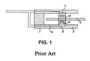
- FIG. 1illustrates a known optical encoder module 1 having a housing 2 , and an emitter (i.e., 9 , 11 ) and a detector 7 that face each other in an aligned relationship.
- the emitter (i.e., 9 , and 11 ) and the detector 7are spaced apart to allow a code wheel 3 to be rotated in the gap formed therebetween.
- the emitter ( 9 , 11 )consists of a light emitting diode (LED) 9 and a separate lens positioned over the LED 9 to receive light from the LED 9 and to produce a beam of light 17 in the direction of the detector 7 .
- LEDlight emitting diode
- the LED 9consists of a semiconductor die of, for example, the GaP or GaAsP type, mounted and electrically coupled via direct or wire bonding to a metal lead-frame 12 . Additionally, the LED 9 may be encapsulated with a transparent epoxy material.
- the separate collimating lens 11is molded from a plastics material and is mounted onto the housing 2 in correct alignment with the LED 9 .
- the detector 7includes four elongated photo-detecting elements that are arranged side-by-side at different angular positions relative to the code wheel 3 so as to receive light from different portions of the light beam 17 . In this way, the encoder module is able to detect both speed and direction of rotation of the code wheel 3 .
- the generation of a collimated beam of light from the emitter (i.e., 9 , 11 ) to the detector 7is an important feature that ensures accurate operation of the encoder. Light straying from the collimated beam is undesirable and contributes to parallax errors in the encoder and degradation of the operational dynamic range of the photo-detecting elements.
- the foregoing design of encoder modulesuffers from various limitations in generating a collimated beam of light from the emitter (i.e., 9 , 11 ) to the detector 7 .
- the collimating lens 11receives light from the LED 9 through a bottom planar surface and focuses light as it exits from the curved top surface. Both the top and bottom surfaces are refracting surfaces that contribute to the collimation of light from LED 9 . Consequently, the ability of the collimating lens to accurately collimate light is limited not just by manufacturing tolerances and inaccuracies in producing the top surface and the bottom surface, but also by the relative positions and orientations of the top and bottom surfaces.
- the position of the collimating lens 11 relative to the LED 9is also critical to the performance of the emitter (i.e., 9 , 11 ) in generating a collimated beam of light. Accurate placement of the lens over the LED 9 is a time consuming process that adds additional cost to the assembly of the encoder module. In addition, inclusion of a collimating lens mounted on the encoder housing limits the ability of manufacturers to design smaller encoders.
- One feature of the present inventionis to provide an optical encoder module that can cause a collimated light beam to be generated from its emitter to its detector.
- Another feature of the present inventionis to provide an optical encoder module that can cause a collimated light beam to be generated from its emitter to its detector and yet has a minimized size and is relatively easy and cost effective to manufacture.
- an optical encoder moduleis employed to detect light modulated by a moveable member (e.g., code wheel).
- the optical encoderincludes an emitter having a light-emitting element, and a transparent medium encapsulating the light-emitting element.
- the transparent mediumhas a convex aspherical external surface shaped so as to focus light received from the light-emitting element into a substantially collimated beam of light using a single refractive interface for illuminating the movable member.
- the optical encode modulealso includes a detector facing the emitter for detecting modulated light of the collimated beam transmitted through the movable member.
- FIG. 1is a cross-sectioned view of a known optical encoder module.
- FIG. 2is a schematic cross-sectional view of an optical encoder module according to one embodiment of the present invention.
- FIG. 3is a perspective cross-sectional view of the optical encoder module of FIG. 2 .
- FIGS. 4A and 4Bare flowcharts showing possible steps for designing a light emitting device in accordance with the invention.
- FIGS. 5 to 8are computer simulation plots showing the refraction of light rays at different stages in the design of a light-emitting device in accordance with one embodiment of the invention.
- FIGS. 2 and 3show an optical encoder module according to one embodiment of the present invention.
- the optical encoder moduleincludes an emitter 80 , a detector 90 , and a code wheel (not shown) positioned in a gap 6 between the emitter 80 and the detector 90 .
- the optical encoder module in accordance with one embodiment of the present inventionis employed to detect light modulated by the code wheel.
- the emitter 80includes a light-emitting element or device (e.g., the diode 120 ), and a transparent medium (e.g., the encapsulant 130 ) encapsulating the light-emitting element 120 .
- the transparent medium 130has a convex aspherical external surface (i.e., the surface 140 ) shaped so as to focus light received from the light-emitting element 120 into a substantially collimated beam of light for illuminating the detector 90 via the code wheel.
- the optical encoder moduleprovides a compact source for generating a collimated beam of light.
- the optical encoder module in accordance with one embodiment of the present inventionallows light to be collimated using a single refractive interface.
- each ray of light from the light-emitting element 120is only refracted once before it enters the collimated beam.
- the single optical interfaceresults in a simpler optical path that in turn results in a greater intensity of light being transmitted to the collimated beam.
- the convex aspherical external surface 140is defined by an expression as follows.
- Ris the distance between a point on the aspherical surface 140 and the optical axis
- Zis the distance between a projection of the point onto the optical axis and the point of intersection between the optical axis and the aspherical surface 140
- mis chosen from the group of whole numbers greater than two
- ris defined by the expression rf*(n1)/n wherein n is the refractive index of the transparent medium 130 , and f is the distance between the light emitting element and the point of intersection between the optical axis and the aspherical surface.
- the transparent encapsulating medium 130is an epoxy compound.
- the convex aspherical external surface 140may be produced by molding the transparent encapsulating medium 130 , such as the epoxy compound.
- the optical encoder modulecan be accurately manufactured using mass production techniques. This makes an optical encoder module according to the invention simpler and cheaper to produce.
- the light-emitting element 120is electrically coupled to a lead-frame 110 , the lead-frame 110 being partially encapsulated by the transparent medium 130 .
- the optical encoder module in accordance with one embodiment of the present inventiondoes not require the accurate placement of any collimating lens during assembly of the encoder.
- the optical encoder module in accordance with one embodiment of the present inventionwill be described in more detail below, also in conjunction with FIGS. 2–8 .
- the optical encoder moduleincludes a housing 100 which is integrally made of a plastic material and comprises two recesses arranged one above the other. Each recess has an open end, and closed end opposite to the open end.
- the gap 6is formed in the housing 100 between the recesses such that it is open to one end of the housing 100 .
- the gap openingis adjacent to the closed end of the recesses.
- the encapsulated optical emitter 80is accommodated within one recess, and the encapsulated optical detector 90 is accommodated within the other recess.
- the encapsulation of the emitter 80 and that of the detector 90have each a locking projection 10 for engaging with respective locking openings 5 to lock the emitter 80 and the detector 90 into a locking position in the respective recesses.
- the encapsulation of the emitter 80 and the detector 90is made of an epoxy material that is transparent to light. This is due to the configuration of the transimpedance amplifier 410 as well as the use of the dummy transimpedance amplifier 420 and the unity gain buffer 440 , which will be described in more detail below, also in conjunction with FIGS. 3–5 .
- the emitter 80 and the detector 90are spaced and aligned to each other such that a code wheel may be rotated through the gap 6 between the emitter 80 and the detector 90 and may be detected and read by the optical encoder module. This alignment is indicated in FIG. 2 by the axis A—A.
- the light emitted by the emitter 80is passed through or blocked by the code wheel and then detected by the detector 90 . Since the emitter 80 and the detector 90 are exactly aligned to each other, i.e. the emitter 80 and the detector 90 are arranged to face each other in an accurate overlapping position, a reliable operation of the optical encoder module is ensured.
- the emitter 80includes the metal lead-frame 110 , the light emitting diode chip 120 , and the molded epoxy encapsulant 130 .
- the LED chip 120is mounted and electrically coupled to two leads of the metal lead frame by any suitable technique known to those in the art, for example by wire bonding.
- the two leadsprovide electrical power to the LED chip 120 such that it may act as a light-emitting element for the emitter 80 .
- the molded epoxy resin compound 130encapsulates the entire LED chip 120 and portions of the lead-frame 110 coupled to the LED chip 120 .
- the encapsulantis molded so as to provide an aspherical lens 135 above the LED chip 120 .
- the aspherical lens 135has an optical axis along the axis A—A, and is shaped such that light emitted by the LED chip 120 is refracted into a collimated beam.
- the aspherical lensis defined by a single lens surface 140 . Surfaces 150 adjacent to the lens 135 are roughened to prevent internal reflection and to reduce stray light rays in the collimated light beam.
- the profile of the convex aspherical external surface 140is defined by the expression:
- Ris the distance between a point on the aspherical surface 140 and the optical axis
- Zis the distance between a projection of the point onto the optical axis and the point of intersection between the optical axis and the aspherical surface 140
- mis chosen from the group of whole numbers greater than two
- ris defined by the expression rf*(n1)/n wherein n is the refractive index of the transparent medium 130 , and f is the distance between the light emitting element and the point of intersection between the optical axis and the aspherical surface.
- nwill be approximately 1.5 for an epoxy encapsulant.
- the distance between the top of the lens surface and the LED chip 120may, for example, be 3 mm, and the largest radius R of the lens may, for example, be 1.3 mm.
- the width of the collimated beam at the detectoris known as the target illumination spot size.
- the specific shape of the lens surfaceis dependent on the value of the constants c and k n . Because of the complexity of the equation, mathematical or computational approaches for deriving the constants c and k n are unsuitable. Instead, the constants are determined empirically using a systematic method illustrated in FIGS. 4A and 4B .
- the flowchartshows a series of steps 400 to 460 suitable for designing a profile for the aspheric lens surface 140 in accordance with the invention.
- the first step 400information concerning the target characteristics of the optical encoder module needs to be gathered. Specifically, the target height h for the encapsulated optical emitter 80 , the illumination spot size w on the encapsulated optical detector 90 , and the refractive index n 1 of the molded epoxy encapsulant 130 need to be determined.
- step 410the target distance between the light emitting element 120 and the point of intersection between the optical axis A—A and the aspherical lens surface 140 is set to a value lower than the height h of the emitter 80 .
- a radius of curvature value ris calculated for the lens in step 420 .
- step 430the profile of the lens is calculated according the prescribed formula using the circular coordinates Z and R.
- the coefficients given in the formulaare determined empirically with the aid of an optics simulation program.
- FIG. 4Billustrates the steps for performing the empirical measurements.
- Steps 440 and 450provide a choice to the designer whether to make the side walls 150 matte to reduce internal reflection rays, and if so whether the matted walls 150 include an absorbing coating.
- step 460illustrates the step of sending the design for fabrication.
- the first step 470 in the empirical measurement processillustrates how the simulation program is programmed to define five elements.
- the first elementis the aspheric lens surface 54 which is determined according to the prescribed formula of step 430 with coefficients d, e, f, g . . . set to zero, and coefficient C set to a non-zero value.
- the second elementis the LED sidewall or emitter body 52 defining an aperture.
- the third elementis the LED base that provides a base for the fourth element, the isotropic point light source 50 located at a distance f from the apex of the lens surface.
- the fifth elementis the detector plane 56 positioned at a distance corresponding to the detector 90 .
- rays of lightare simulated by the optics simulation program being emitted from the point light source 50 in a single plane between 0 degrees and 180 degrees at fixed angular intervals.
- the programsimulates refraction of the light rays by the aspheric lens surface element 54 towards the detector 56 .
- step 480the coefficient C is first optimised by adjusting its value until the rays of light are collimated as close to the optical axis as possible. At this stage the other coefficients or constants are set to zero.
- each constantis then optimised in turn, i.e. with increasing n, until the beam of light is optimised as a substantially collimated beam of light. If one constant has been adjusted significantly, the previous constant may need to be re-optimised as shown in steps 493 and 497 .
- the distribution of the light rays on the detector planeis analysed to assess whether a majority are evenly distributed across the specified spot size w. If so, the coefficients are successfully optimised.
- FIG. 5shows the simulated light rays for an unoptimised value of c
- FIG. 6shows the light rays for an optimised value of c
- FIG. 7shows the light rays for an optimised value of d
Landscapes
- Physics & Mathematics (AREA)
- General Physics & Mathematics (AREA)
- Optical Transform (AREA)
Abstract
Description
wherein R is the distance between a point on the
rf*(n1)/n
wherein n is the refractive index of the
wherein R is the distance between a point on the
rf*(n1)/n
wherein n is the refractive index of the
Claims (9)
Priority Applications (1)
| Application Number | Priority Date | Filing Date | Title |
|---|---|---|---|
| US10/344,836US7279674B2 (en) | 2000-08-17 | 2001-08-15 | Optical encoder module |
Applications Claiming Priority (4)
| Application Number | Priority Date | Filing Date | Title |
|---|---|---|---|
| MYPI20003785 | 2000-08-17 | ||
| MYPI20003785 | 2000-08-17 | ||
| US10/344,836US7279674B2 (en) | 2000-08-17 | 2001-08-15 | Optical encoder module |
| PCT/US2001/025599WO2002014794A1 (en) | 2000-08-17 | 2001-08-15 | Optical encoder module |
Publications (2)
| Publication Number | Publication Date |
|---|---|
| US20050068773A1 US20050068773A1 (en) | 2005-03-31 |
| US7279674B2true US7279674B2 (en) | 2007-10-09 |
Family
ID=34380497
Family Applications (1)
| Application Number | Title | Priority Date | Filing Date |
|---|---|---|---|
| US10/344,836Expired - Fee RelatedUS7279674B2 (en) | 2000-08-17 | 2001-08-15 | Optical encoder module |
Country Status (1)
| Country | Link |
|---|---|
| US (1) | US7279674B2 (en) |
Cited By (2)
| Publication number | Priority date | Publication date | Assignee | Title |
|---|---|---|---|---|
| US20100123071A1 (en)* | 2008-11-19 | 2010-05-20 | Lin Hui-Chin | Transmissive optical encoder |
| US20110031383A1 (en)* | 2009-08-04 | 2011-02-10 | Mitutoyo Corporation | lens aberration correction in a doubly telecentric displacement sensor |
Families Citing this family (1)
| Publication number | Priority date | Publication date | Assignee | Title |
|---|---|---|---|---|
| US7507981B2 (en)* | 2006-05-30 | 2009-03-24 | Avago Technologies Ecbu Ip (Singapore) Pte. Ltd. | System for identifying a characteristic of a printing media |
Citations (30)
| Publication number | Priority date | Publication date | Assignee | Title |
|---|---|---|---|---|
| US3903218A (en) | 1972-03-16 | 1975-09-02 | Humphrey Instruments Inc | Method for constructing variable anamorphic lens |
| US4190767A (en)* | 1978-06-26 | 1980-02-26 | Trw Inc. | Optical encoder apparatus |
| JPS61254915A (en) | 1985-05-03 | 1986-11-12 | Canon Inc | Optical system for adjusting diameter of luminous flux |
| US4691101A (en) | 1985-06-19 | 1987-09-01 | Hewlett-Packard Company | Optical positional encoder comprising immediately adjacent detectors |
| JPH01109317A (en) | 1987-10-23 | 1989-04-26 | Matsushita Electric Ind Co Ltd | Collimator single lens |
| US4915484A (en) | 1987-04-06 | 1990-04-10 | Matsushita Electric Industrial Co., Ltd. | Anamorphic single lens |
| USD329193S (en) | 1989-06-30 | 1992-09-08 | Hewlett-Packard Company | Optical encoder bracket |
| JPH0529660A (en) | 1990-09-07 | 1993-02-05 | Toshiba Corp | LED lamp |
| US5241172A (en)* | 1991-11-04 | 1993-08-31 | Hewlett-Packard Company | Variable pitch position encoder |
| JPH0612677A (en) | 1991-12-16 | 1994-01-21 | Koji Kaneoka | Method for recording, reading and outputting optical disk |
| US5289082A (en) | 1990-09-07 | 1994-02-22 | Kabushiki Kaisha Toshiba | LED lamp |
| US5291038A (en)* | 1990-12-19 | 1994-03-01 | Sharp Kabushiki Kaisha | Reflective type photointerrupter |
| US5317149A (en)* | 1992-11-12 | 1994-05-31 | Hewlett-Packard Company | Optical encoder with encapsulated electrooptics |
| JPH06224859A (en) | 1992-11-23 | 1994-08-12 | Hewlett Packard Co <Hp> | Optical transceiver with improved range and improved data signaling speed |
| US5589930A (en) | 1991-09-13 | 1996-12-31 | Nippondenso Co., Ltd. | Optical radar apparatus |
| JPH09258099A (en) | 1996-03-21 | 1997-10-03 | Matsushita Electric Ind Co Ltd | Anisotropic refractive power single lens and optical head device using the same, information recording / reproducing device, scanning optical device, image forming device and optical fiber coupling device |
| JPH10178393A (en) | 1996-10-14 | 1998-06-30 | Ricoh Co Ltd | Optical transceiver |
| US5841177A (en) | 1993-06-25 | 1998-11-24 | Kabushiki Kaisha Toshiba | Multicolor light emitting device |
| US5898267A (en) | 1996-04-10 | 1999-04-27 | Mcdermott; Kevin | Parabolic axial lighting device |
| US5986788A (en) | 1995-06-26 | 1999-11-16 | Oki Electric Industry Co., Inc. | Microoptical system for free-space optical interconnection and its setting method |
| JP2000294832A (en) | 1999-04-05 | 2000-10-20 | Matsushita Electronics Industry Corp | Light emitting diode device and method of manufacturing the same |
| JP2000294838A (en) | 1999-04-07 | 2000-10-20 | Matsushita Electronics Industry Corp | Chip type light emitting diode array |
| US6335548B1 (en) | 1999-03-15 | 2002-01-01 | Gentex Corporation | Semiconductor radiation emitter package |
| US6410911B1 (en)* | 1999-05-12 | 2002-06-25 | Mitutoyo Corporation | Optical displacement detecting apparatus |
| US20030156842A1 (en) | 2002-02-18 | 2003-08-21 | Keiji Morimoto | Infrared communication module with remote control transmission function |
| US6617615B1 (en)* | 1999-11-01 | 2003-09-09 | Rohm Co., Ltd. | Semiconductor light-emitting device |
| US6627869B2 (en) | 2001-04-24 | 2003-09-30 | Matsushita Electric Industrial Co., Ltd. | Beam shaper, and semiconductor laser source device and optical head using the beam shaper |
| US20040165277A1 (en) | 2003-02-25 | 2004-08-26 | Ng Peng Yam | Single lens multiple light source device |
| US6876471B1 (en) | 1999-06-08 | 2005-04-05 | Fuji Photo Film Co., Ltd. | Image reading device |
| US6979104B2 (en) | 2001-12-31 | 2005-12-27 | R.J. Doran & Co. LTD | LED inspection lamp |
Family Cites Families (1)
| Publication number | Priority date | Publication date | Assignee | Title |
|---|---|---|---|---|
| US329193A (en)* | 1885-10-27 | Horseshoe-pad |
- 2001
- 2001-08-15USUS10/344,836patent/US7279674B2/ennot_activeExpired - Fee Related
Patent Citations (31)
| Publication number | Priority date | Publication date | Assignee | Title |
|---|---|---|---|---|
| US3903218A (en) | 1972-03-16 | 1975-09-02 | Humphrey Instruments Inc | Method for constructing variable anamorphic lens |
| US4190767A (en)* | 1978-06-26 | 1980-02-26 | Trw Inc. | Optical encoder apparatus |
| JPS61254915A (en) | 1985-05-03 | 1986-11-12 | Canon Inc | Optical system for adjusting diameter of luminous flux |
| US4691101A (en) | 1985-06-19 | 1987-09-01 | Hewlett-Packard Company | Optical positional encoder comprising immediately adjacent detectors |
| US4915484A (en) | 1987-04-06 | 1990-04-10 | Matsushita Electric Industrial Co., Ltd. | Anamorphic single lens |
| JPH01109317A (en) | 1987-10-23 | 1989-04-26 | Matsushita Electric Ind Co Ltd | Collimator single lens |
| USD329193S (en) | 1989-06-30 | 1992-09-08 | Hewlett-Packard Company | Optical encoder bracket |
| JPH0529660A (en) | 1990-09-07 | 1993-02-05 | Toshiba Corp | LED lamp |
| US5289082A (en) | 1990-09-07 | 1994-02-22 | Kabushiki Kaisha Toshiba | LED lamp |
| US5291038A (en)* | 1990-12-19 | 1994-03-01 | Sharp Kabushiki Kaisha | Reflective type photointerrupter |
| US5589930A (en) | 1991-09-13 | 1996-12-31 | Nippondenso Co., Ltd. | Optical radar apparatus |
| US5241172A (en)* | 1991-11-04 | 1993-08-31 | Hewlett-Packard Company | Variable pitch position encoder |
| JPH0612677A (en) | 1991-12-16 | 1994-01-21 | Koji Kaneoka | Method for recording, reading and outputting optical disk |
| US5317149A (en)* | 1992-11-12 | 1994-05-31 | Hewlett-Packard Company | Optical encoder with encapsulated electrooptics |
| US5495358A (en) | 1992-11-23 | 1996-02-27 | Hewlett-Packard Company | Optical transceiver with improved range and data communication rate |
| JPH06224859A (en) | 1992-11-23 | 1994-08-12 | Hewlett Packard Co <Hp> | Optical transceiver with improved range and improved data signaling speed |
| US5841177A (en) | 1993-06-25 | 1998-11-24 | Kabushiki Kaisha Toshiba | Multicolor light emitting device |
| US5986788A (en) | 1995-06-26 | 1999-11-16 | Oki Electric Industry Co., Inc. | Microoptical system for free-space optical interconnection and its setting method |
| JPH09258099A (en) | 1996-03-21 | 1997-10-03 | Matsushita Electric Ind Co Ltd | Anisotropic refractive power single lens and optical head device using the same, information recording / reproducing device, scanning optical device, image forming device and optical fiber coupling device |
| US5898267A (en) | 1996-04-10 | 1999-04-27 | Mcdermott; Kevin | Parabolic axial lighting device |
| JPH10178393A (en) | 1996-10-14 | 1998-06-30 | Ricoh Co Ltd | Optical transceiver |
| US6335548B1 (en) | 1999-03-15 | 2002-01-01 | Gentex Corporation | Semiconductor radiation emitter package |
| JP2000294832A (en) | 1999-04-05 | 2000-10-20 | Matsushita Electronics Industry Corp | Light emitting diode device and method of manufacturing the same |
| JP2000294838A (en) | 1999-04-07 | 2000-10-20 | Matsushita Electronics Industry Corp | Chip type light emitting diode array |
| US6410911B1 (en)* | 1999-05-12 | 2002-06-25 | Mitutoyo Corporation | Optical displacement detecting apparatus |
| US6876471B1 (en) | 1999-06-08 | 2005-04-05 | Fuji Photo Film Co., Ltd. | Image reading device |
| US6617615B1 (en)* | 1999-11-01 | 2003-09-09 | Rohm Co., Ltd. | Semiconductor light-emitting device |
| US6627869B2 (en) | 2001-04-24 | 2003-09-30 | Matsushita Electric Industrial Co., Ltd. | Beam shaper, and semiconductor laser source device and optical head using the beam shaper |
| US6979104B2 (en) | 2001-12-31 | 2005-12-27 | R.J. Doran & Co. LTD | LED inspection lamp |
| US20030156842A1 (en) | 2002-02-18 | 2003-08-21 | Keiji Morimoto | Infrared communication module with remote control transmission function |
| US20040165277A1 (en) | 2003-02-25 | 2004-08-26 | Ng Peng Yam | Single lens multiple light source device |
Non-Patent Citations (2)
| Title |
|---|
| English translation of Japan Office Action dated Mar. 14, 2006 involving Japan Application No. 2004-041597 (co-pending application). |
| Japan Office Action dated Mar. 14, 2006 involving Japan Application No. 2004-041597 (co-pending application). |
Cited By (4)
| Publication number | Priority date | Publication date | Assignee | Title |
|---|---|---|---|---|
| US20100123071A1 (en)* | 2008-11-19 | 2010-05-20 | Lin Hui-Chin | Transmissive optical encoder |
| US8258460B2 (en)* | 2008-11-19 | 2012-09-04 | Everlight Electronics Co., Ltd. | Transmissive optical encoder |
| US20110031383A1 (en)* | 2009-08-04 | 2011-02-10 | Mitutoyo Corporation | lens aberration correction in a doubly telecentric displacement sensor |
| US8492703B2 (en)* | 2009-08-04 | 2013-07-23 | Mitutoyo Corporation | Lens aberration correction in a doubly telecentric displacement sensor |
Also Published As
| Publication number | Publication date |
|---|---|
| US20050068773A1 (en) | 2005-03-31 |
Similar Documents
| Publication | Publication Date | Title |
|---|---|---|
| CN101655350B (en) | Optical distance measuring sensor and electronic device | |
| US5130531A (en) | Reflective photosensor and semiconductor light emitting apparatus each using micro Fresnel lens | |
| JP5327980B2 (en) | Optical proximity sensor with improved shield and lens | |
| US12218294B2 (en) | Light source device | |
| US7795576B2 (en) | Single dome lens reflective optical encoder | |
| US8188421B2 (en) | Optical encoder for detecting the relative displacement between an encoder scale and an encoder head | |
| JP4976823B2 (en) | Optical encoder | |
| US9383229B2 (en) | Optical reflective encoder with multi-faceted flat-faced lens | |
| WO2002052656A1 (en) | Led module | |
| CN100535606C (en) | Optical Encoder | |
| JP4726168B2 (en) | Optical scale and optical encoder | |
| US6410911B1 (en) | Optical displacement detecting apparatus | |
| US7279674B2 (en) | Optical encoder module | |
| US7784694B2 (en) | Reflective encoder with lens on code strip | |
| JP5085001B2 (en) | Optical encoder module | |
| JP2005049345A (en) | Optical displacement sensor | |
| JPH10144966A (en) | Light emitting diode | |
| US6984837B2 (en) | Optical telemeter target illumination apparatus with edge emitter light source | |
| JP3704459B2 (en) | Semiconductor laser device and manufacturing method thereof | |
| JP4694677B2 (en) | Optical encoder | |
| JPH10209490A (en) | Reflective optical coupling device | |
| JP3854299B2 (en) | Optical coupling device | |
| JP3729725B2 (en) | Optical coupling device | |
| JP2001111154A (en) | Semiconductor laser device | |
| JP3600462B2 (en) | Method for manufacturing hologram element |
Legal Events
| Date | Code | Title | Description |
|---|---|---|---|
| AS | Assignment | Owner name:AGILENT TECHNOLOGIES, INC., COLORADO Free format text:ASSIGNMENT OF ASSIGNORS INTEREST;ASSIGNORS:NG, KEE-YEAN;FO, KOK-HING;CHIN, YEE-LOONG;AND OTHERS;REEL/FRAME:014358/0568 Effective date:20030127 | |
| AS | Assignment | Owner name:AVAGO TECHNOLOGIES GENERAL IP PTE. LTD.,SINGAPORE Free format text:ASSIGNMENT OF ASSIGNORS INTEREST;ASSIGNOR:AGILENT TECHNOLOGIES, INC.;REEL/FRAME:017206/0666 Effective date:20051201 Owner name:AVAGO TECHNOLOGIES GENERAL IP PTE. LTD., SINGAPORE Free format text:ASSIGNMENT OF ASSIGNORS INTEREST;ASSIGNOR:AGILENT TECHNOLOGIES, INC.;REEL/FRAME:017206/0666 Effective date:20051201 | |
| AS | Assignment | Owner name:AVAGO TECHNOLOGIES ECBU IP (SINGAPORE) PTE. LTD., SINGAPORE Free format text:ASSIGNMENT OF ASSIGNORS INTEREST;ASSIGNOR:AVAGO TECHNOLOGIES GENERAL IP (SINGAPORE) PTE. LTD.;REEL/FRAME:017675/0518 Effective date:20060127 Owner name:AVAGO TECHNOLOGIES ECBU IP (SINGAPORE) PTE. LTD.,S Free format text:ASSIGNMENT OF ASSIGNORS INTEREST;ASSIGNOR:AVAGO TECHNOLOGIES GENERAL IP (SINGAPORE) PTE. LTD.;REEL/FRAME:017675/0518 Effective date:20060127 Owner name:AVAGO TECHNOLOGIES ECBU IP (SINGAPORE) PTE. LTD., Free format text:ASSIGNMENT OF ASSIGNORS INTEREST;ASSIGNOR:AVAGO TECHNOLOGIES GENERAL IP (SINGAPORE) PTE. LTD.;REEL/FRAME:017675/0518 Effective date:20060127 | |
| FPAY | Fee payment | Year of fee payment:4 | |
| CC | Certificate of correction | ||
| AS | Assignment | Owner name:AVAGO TECHNOLOGIES GENERAL IP (SINGAPORE) PTE. LTD Free format text:MERGER;ASSIGNOR:AVAGO TECHNOLOGIES ECBU IP (SINGAPORE) PTE. LTD.;REEL/FRAME:030369/0528 Effective date:20121030 | |
| REMI | Maintenance fee reminder mailed | ||
| LAPS | Lapse for failure to pay maintenance fees | ||
| STCH | Information on status: patent discontinuation | Free format text:PATENT EXPIRED DUE TO NONPAYMENT OF MAINTENANCE FEES UNDER 37 CFR 1.362 | |
| FP | Lapsed due to failure to pay maintenance fee | Effective date:20151009 | |
| AS | Assignment | Owner name:AVAGO TECHNOLOGIES GENERAL IP (SINGAPORE) PTE. LTD Free format text:CORRECTIVE ASSIGNMENT TO CORRECT THE ASSIGNEE NAME PREVIOUSLY RECORDED AT REEL: 017206 FRAME: 0666. ASSIGNOR(S) HEREBY CONFIRMS THE ASSIGNMENT;ASSIGNOR:AGILENT TECHNOLOGIES, INC.;REEL/FRAME:038632/0662 Effective date:20051201 |