US7279432B2 - System and method for forming an integrated barrier layer - Google Patents
System and method for forming an integrated barrier layerDownload PDFInfo
- Publication number
- US7279432B2 US7279432B2US10/414,271US41427103AUS7279432B2US 7279432 B2US7279432 B2US 7279432B2US 41427103 AUS41427103 AUS 41427103AUS 7279432 B2US7279432 B2US 7279432B2
- Authority
- US
- United States
- Prior art keywords
- tungsten
- layer
- deposition process
- substrate
- refractory metal
- Prior art date
- Legal status (The legal status is an assumption and is not a legal conclusion. Google has not performed a legal analysis and makes no representation as to the accuracy of the status listed.)
- Expired - Lifetime, expires
Links
- 238000000034methodMethods0.000titleclaimsabstractdescription146
- 230000004888barrier functionEffects0.000titleabstractdescription61
- 230000008569processEffects0.000claimsabstractdescription119
- 238000000151depositionMethods0.000claimsabstractdescription68
- 238000005229chemical vapour depositionMethods0.000claimsabstractdescription61
- 239000000758substrateSubstances0.000claimsabstractdescription54
- 238000005137deposition processMethods0.000claimsabstractdescription50
- 230000008021depositionEffects0.000claimsabstractdescription39
- 239000007789gasSubstances0.000claimsdescription123
- 239000002243precursorSubstances0.000claimsdescription60
- WFKWXMTUELFFGS-UHFFFAOYSA-NtungstenChemical compound[W]WFKWXMTUELFFGS-UHFFFAOYSA-N0.000claimsdescription35
- 229910052721tungstenInorganic materials0.000claimsdescription35
- 239000010937tungstenSubstances0.000claimsdescription35
- 229910052751metalInorganic materials0.000claimsdescription31
- 239000002184metalSubstances0.000claimsdescription31
- 239000000463materialSubstances0.000claimsdescription30
- 238000009826distributionMethods0.000claimsdescription25
- BLRPTPMANUNPDV-UHFFFAOYSA-NSilaneChemical compound[SiH4]BLRPTPMANUNPDV-UHFFFAOYSA-N0.000claimsdescription16
- NRTOMJZYCJJWKI-UHFFFAOYSA-NTitanium nitrideChemical compound[Ti]#NNRTOMJZYCJJWKI-UHFFFAOYSA-N0.000claimsdescription16
- RTAQQCXQSZGOHL-UHFFFAOYSA-NTitaniumChemical compound[Ti]RTAQQCXQSZGOHL-UHFFFAOYSA-N0.000claimsdescription9
- 238000001465metallisationMethods0.000claimsdescription9
- 229910000077silaneInorganic materials0.000claimsdescription9
- 229910052715tantalumInorganic materials0.000claimsdescription9
- GUVRBAGPIYLISA-UHFFFAOYSA-Ntantalum atomChemical compound[Ta]GUVRBAGPIYLISA-UHFFFAOYSA-N0.000claimsdescription9
- 239000010936titaniumSubstances0.000claimsdescription8
- NXHILIPIEUBEPD-UHFFFAOYSA-Htungsten hexafluorideChemical groupF[W](F)(F)(F)(F)FNXHILIPIEUBEPD-UHFFFAOYSA-H0.000claimsdescription8
- QGZKDVFQNNGYKY-UHFFFAOYSA-NAmmoniaChemical compoundNQGZKDVFQNNGYKY-UHFFFAOYSA-N0.000claimsdescription7
- UORVGPXVDQYIDP-UHFFFAOYSA-NboraneChemical compoundBUORVGPXVDQYIDP-UHFFFAOYSA-N0.000claimsdescription7
- -1diboraneChemical compound0.000claimsdescription7
- 229910052719titaniumInorganic materials0.000claimsdescription7
- OFEAOSSMQHGXMM-UHFFFAOYSA-N12007-10-2Chemical compound[W].[W]=[B]OFEAOSSMQHGXMM-UHFFFAOYSA-N0.000claimsdescription5
- 229910000085boraneInorganic materials0.000claimsdescription4
- 238000011049fillingMethods0.000claimsdescription4
- 229910021529ammoniaInorganic materials0.000claimsdescription3
- PZPGRFITIJYNEJ-UHFFFAOYSA-NdisilaneChemical compound[SiH3][SiH3]PZPGRFITIJYNEJ-UHFFFAOYSA-N0.000claimsdescription3
- 239000001257hydrogenSubstances0.000claimsdescription3
- 229910052739hydrogenInorganic materials0.000claimsdescription3
- 125000004435hydrogen atomChemical class[H]*0.000claimsdescription3
- MZLGASXMSKOWSE-UHFFFAOYSA-Ntantalum nitrideChemical compound[Ta]#NMZLGASXMSKOWSE-UHFFFAOYSA-N0.000claimsdescription3
- 239000003638chemical reducing agentSubstances0.000claims2
- 238000005019vapor deposition processMethods0.000claims2
- 239000003870refractory metalSubstances0.000abstractdescription88
- 239000010410layerSubstances0.000description175
- 239000010949copperSubstances0.000description30
- 239000003990capacitorSubstances0.000description23
- 239000012159carrier gasSubstances0.000description21
- RYGMFSIKBFXOCR-UHFFFAOYSA-NCopperChemical compound[Cu]RYGMFSIKBFXOCR-UHFFFAOYSA-N0.000description19
- 229910052802copperInorganic materials0.000description19
- NJPPVKZQTLUDBO-UHFFFAOYSA-NnovaluronChemical compoundC1=C(Cl)C(OC(F)(F)C(OC(F)(F)F)F)=CC=C1NC(=O)NC(=O)C1=C(F)C=CC=C1FNJPPVKZQTLUDBO-UHFFFAOYSA-N0.000description19
- 229910021420polycrystalline siliconInorganic materials0.000description16
- 229920005591polysiliconPolymers0.000description16
- 238000004519manufacturing processMethods0.000description15
- XKRFYHLGVUSROY-UHFFFAOYSA-NArgonChemical compound[Ar]XKRFYHLGVUSROY-UHFFFAOYSA-N0.000description14
- 238000010926purgeMethods0.000description14
- 239000003989dielectric materialSubstances0.000description13
- XUIMIQQOPSSXEZ-UHFFFAOYSA-NSiliconChemical compound[Si]XUIMIQQOPSSXEZ-UHFFFAOYSA-N0.000description11
- 229910052710siliconInorganic materials0.000description11
- 239000010703siliconSubstances0.000description11
- 230000015572biosynthetic processEffects0.000description9
- MNWRORMXBIWXCI-UHFFFAOYSA-Ntetrakis(dimethylamido)titaniumChemical compoundCN(C)[Ti](N(C)C)(N(C)C)N(C)CMNWRORMXBIWXCI-UHFFFAOYSA-N0.000description8
- 229910052786argonInorganic materials0.000description7
- VYPSYNLAJGMNEJ-UHFFFAOYSA-NSilicium dioxideChemical compoundO=[Si]=OVYPSYNLAJGMNEJ-UHFFFAOYSA-N0.000description6
- 229910052814silicon oxideInorganic materials0.000description6
- 229910052581Si3N4Inorganic materials0.000description5
- 229910052782aluminiumInorganic materials0.000description5
- XAGFODPZIPBFFR-UHFFFAOYSA-NaluminiumChemical compound[Al]XAGFODPZIPBFFR-UHFFFAOYSA-N0.000description5
- 239000004065semiconductorSubstances0.000description5
- HQVNEWCFYHHQES-UHFFFAOYSA-Nsilicon nitrideChemical compoundN12[Si]34N5[Si]62N3[Si]51N64HQVNEWCFYHHQES-UHFFFAOYSA-N0.000description5
- POILWHVDKZOXJZ-ARJAWSKDSA-M(z)-4-oxopent-2-en-2-olateChemical compoundC\C([O-])=C\C(C)=OPOILWHVDKZOXJZ-ARJAWSKDSA-M0.000description4
- QGHDLJAZIIFENW-UHFFFAOYSA-N4-[1,1,1,3,3,3-hexafluoro-2-(4-hydroxy-3-prop-2-enylphenyl)propan-2-yl]-2-prop-2-enylphenolChemical groupC1=C(CC=C)C(O)=CC=C1C(C(F)(F)F)(C(F)(F)F)C1=CC=C(O)C(CC=C)=C1QGHDLJAZIIFENW-UHFFFAOYSA-N0.000description4
- JBRZTFJDHDCESZ-UHFFFAOYSA-NAsGaChemical compound[As]#[Ga]JBRZTFJDHDCESZ-UHFFFAOYSA-N0.000description4
- 229910052454barium strontium titanateInorganic materials0.000description4
- ZOCHARZZJNPSEU-UHFFFAOYSA-NdiboronChemical compoundB#BZOCHARZZJNPSEU-UHFFFAOYSA-N0.000description4
- 238000009792diffusion processMethods0.000description4
- 229910052732germaniumInorganic materials0.000description4
- GNPVGFCGXDBREM-UHFFFAOYSA-Ngermanium atomChemical compound[Ge]GNPVGFCGXDBREM-UHFFFAOYSA-N0.000description4
- 229910052451lead zirconate titanateInorganic materials0.000description4
- TWNQGVIAIRXVLR-UHFFFAOYSA-Noxo(oxoalumanyloxy)alumaneChemical compoundO=[Al]O[Al]=OTWNQGVIAIRXVLR-UHFFFAOYSA-N0.000description4
- BPUBBGLMJRNUCC-UHFFFAOYSA-Noxygen(2-);tantalum(5+)Chemical compound[O-2].[O-2].[O-2].[O-2].[O-2].[Ta+5].[Ta+5]BPUBBGLMJRNUCC-UHFFFAOYSA-N0.000description4
- 238000005240physical vapour depositionMethods0.000description4
- PBCFLUZVCVVTBY-UHFFFAOYSA-Ntantalum pentoxideInorganic materialsO=[Ta](=O)O[Ta](=O)=OPBCFLUZVCVVTBY-UHFFFAOYSA-N0.000description4
- OAKJQQAXSVQMHS-UHFFFAOYSA-NHydrazineChemical compoundNNOAKJQQAXSVQMHS-UHFFFAOYSA-N0.000description3
- 239000001307heliumSubstances0.000description3
- 229910052734heliumInorganic materials0.000description3
- SWQJXJOGLNCZEY-UHFFFAOYSA-Nhelium atomChemical compound[He]SWQJXJOGLNCZEY-UHFFFAOYSA-N0.000description3
- 239000000376reactantSubstances0.000description3
- 238000003860storageMethods0.000description3
- IJGRMHOSHXDMSA-UHFFFAOYSA-NAtomic nitrogenChemical compoundN#NIJGRMHOSHXDMSA-UHFFFAOYSA-N0.000description2
- RKFJZNPFHXIBTP-UHFFFAOYSA-N[Cu].CCC(F)(F)C(F)(F)C(F)=C(F)C(F)=C(C)CChemical compound[Cu].CCC(F)(F)C(F)(F)C(F)=C(F)C(F)=C(C)CRKFJZNPFHXIBTP-UHFFFAOYSA-N0.000description2
- VNSWULZVUKFJHK-UHFFFAOYSA-N[Sr].[Bi]Chemical compound[Sr].[Bi]VNSWULZVUKFJHK-UHFFFAOYSA-N0.000description2
- 229910002113barium titanateInorganic materials0.000description2
- JRPBQTZRNDNNOP-UHFFFAOYSA-Nbarium titanateChemical compound[Ba+2].[Ba+2].[O-][Ti]([O-])([O-])[O-]JRPBQTZRNDNNOP-UHFFFAOYSA-N0.000description2
- 229910002115bismuth titanateInorganic materials0.000description2
- FQNHWXHRAUXLFU-UHFFFAOYSA-Ncarbon monoxide;tungstenChemical compound[W].[O+]#[C-].[O+]#[C-].[O+]#[C-].[O+]#[C-].[O+]#[C-].[O+]#[C-]FQNHWXHRAUXLFU-UHFFFAOYSA-N0.000description2
- 238000006243chemical reactionMethods0.000description2
- TUTOKIOKAWTABR-UHFFFAOYSA-NdimethylalumaneChemical compoundC[AlH]CTUTOKIOKAWTABR-UHFFFAOYSA-N0.000description2
- 238000005530etchingMethods0.000description2
- GCSJLQSCSDMKTP-UHFFFAOYSA-Nethenyl(trimethyl)silaneChemical compoundC[Si](C)(C)C=CGCSJLQSCSDMKTP-UHFFFAOYSA-N0.000description2
- 239000011810insulating materialSubstances0.000description2
- HFGPZNIAWCZYJU-UHFFFAOYSA-Nlead zirconate titanateChemical compound[O-2].[O-2].[O-2].[O-2].[O-2].[Ti+4].[Zr+4].[Pb+2]HFGPZNIAWCZYJU-UHFFFAOYSA-N0.000description2
- 238000001459lithographyMethods0.000description2
- 238000002156mixingMethods0.000description2
- VEALVRVVWBQVSL-UHFFFAOYSA-Nstrontium titanateChemical compound[Sr+2].[O-][Ti]([O-])=OVEALVRVVWBQVSL-UHFFFAOYSA-N0.000description2
- XJDNKRIXUMDJCW-UHFFFAOYSA-Jtitanium tetrachlorideChemical compoundCl[Ti](Cl)(Cl)ClXJDNKRIXUMDJCW-UHFFFAOYSA-J0.000description2
- DIIIISSCIXVANO-UHFFFAOYSA-N1,2-DimethylhydrazineChemical compoundCNNCDIIIISSCIXVANO-UHFFFAOYSA-N0.000description1
- ZOXJGFHDIHLPTG-UHFFFAOYSA-NBoronChemical compound[B]ZOXJGFHDIHLPTG-UHFFFAOYSA-N0.000description1
- 229910003915SiCl2H2Inorganic materials0.000description1
- 230000004913activationEffects0.000description1
- 229910021417amorphous siliconInorganic materials0.000description1
- 238000000137annealingMethods0.000description1
- 229910052787antimonyInorganic materials0.000description1
- WATWJIUSRGPENY-UHFFFAOYSA-Nantimony atomChemical compound[Sb]WATWJIUSRGPENY-UHFFFAOYSA-N0.000description1
- 229910052785arsenicInorganic materials0.000description1
- RQNWIZPPADIBDY-UHFFFAOYSA-Narsenic atomChemical compound[As]RQNWIZPPADIBDY-UHFFFAOYSA-N0.000description1
- IVHJCRXBQPGLOV-UHFFFAOYSA-NazanylidynetungstenChemical compound[W]#NIVHJCRXBQPGLOV-UHFFFAOYSA-N0.000description1
- 230000008901benefitEffects0.000description1
- 229910052796boronInorganic materials0.000description1
- 239000006227byproductSubstances0.000description1
- 238000009833condensationMethods0.000description1
- 230000005494condensationEffects0.000description1
- 238000010586diagramMethods0.000description1
- MROCJMGDEKINLD-UHFFFAOYSA-NdichlorosilaneChemical compoundCl[SiH2]ClMROCJMGDEKINLD-UHFFFAOYSA-N0.000description1
- 238000006073displacement reactionMethods0.000description1
- GKCPCPKXFGQXGS-UHFFFAOYSA-Nditert-butyldiazeneChemical compoundCC(C)(C)N=NC(C)(C)CGKCPCPKXFGQXGS-UHFFFAOYSA-N0.000description1
- 239000002019doping agentSubstances0.000description1
- AIGRXSNSLVJMEA-FQEVSTJZSA-Nethoxy-(4-nitrophenoxy)-phenyl-sulfanylidene-$l^{5}-phosphaneChemical compoundO([P@@](=S)(OCC)C=1C=CC=CC=1)C1=CC=C([N+]([O-])=O)C=C1AIGRXSNSLVJMEA-FQEVSTJZSA-N0.000description1
- UCSVJZQSZZAKLD-UHFFFAOYSA-Nethyl azideChemical compoundCCN=[N+]=[N-]UCSVJZQSZZAKLD-UHFFFAOYSA-N0.000description1
- 238000010438heat treatmentMethods0.000description1
- BHEPBYXIRTUNPN-UHFFFAOYSA-Nhydridophosphorus(.) (triplet)Chemical compound[PH]BHEPBYXIRTUNPN-UHFFFAOYSA-N0.000description1
- 239000012212insulatorSubstances0.000description1
- 230000007246mechanismEffects0.000description1
- HDZGCSFEDULWCS-UHFFFAOYSA-NmonomethylhydrazineChemical compoundCNNHDZGCSFEDULWCS-UHFFFAOYSA-N0.000description1
- 229910000069nitrogen hydrideInorganic materials0.000description1
- NFHFRUOZVGFOOS-UHFFFAOYSA-Npalladium;triphenylphosphaneChemical compound[Pd].C1=CC=CC=C1P(C=1C=CC=CC=1)C1=CC=CC=C1.C1=CC=CC=C1P(C=1C=CC=CC=1)C1=CC=CC=C1.C1=CC=CC=C1P(C=1C=CC=CC=1)C1=CC=CC=C1.C1=CC=CC=C1P(C=1C=CC=CC=1)C1=CC=CC=C1NFHFRUOZVGFOOS-UHFFFAOYSA-N0.000description1
- 239000002245particleSubstances0.000description1
- HKOOXMFOFWEVGF-UHFFFAOYSA-NphenylhydrazineChemical compoundNNC1=CC=CC=C1HKOOXMFOFWEVGF-UHFFFAOYSA-N0.000description1
- 229940067157phenylhydrazineDrugs0.000description1
- 230000009257reactivityEffects0.000description1
- 238000009877renderingMethods0.000description1
- 239000002356single layerSubstances0.000description1
- 238000001179sorption measurementMethods0.000description1
- MUQNAPSBHXFMHT-UHFFFAOYSA-Ntert-butylhydrazineChemical compoundCC(C)(C)NNMUQNAPSBHXFMHT-UHFFFAOYSA-N0.000description1
- 238000005979thermal decomposition reactionMethods0.000description1
- 239000011800void materialSubstances0.000description1
Images


Classifications
- H—ELECTRICITY
- H01—ELECTRIC ELEMENTS
- H01L—SEMICONDUCTOR DEVICES NOT COVERED BY CLASS H10
- H01L21/00—Processes or apparatus adapted for the manufacture or treatment of semiconductor or solid state devices or of parts thereof
- H01L21/70—Manufacture or treatment of devices consisting of a plurality of solid state components formed in or on a common substrate or of parts thereof; Manufacture of integrated circuit devices or of parts thereof
- H01L21/71—Manufacture of specific parts of devices defined in group H01L21/70
- H01L21/768—Applying interconnections to be used for carrying current between separate components within a device comprising conductors and dielectrics
- H01L21/76838—Applying interconnections to be used for carrying current between separate components within a device comprising conductors and dielectrics characterised by the formation and the after-treatment of the conductors
- H01L21/76841—Barrier, adhesion or liner layers
- H01L21/76843—Barrier, adhesion or liner layers formed in openings in a dielectric
- H01L21/76846—Layer combinations
- H—ELECTRICITY
- H01—ELECTRIC ELEMENTS
- H01L—SEMICONDUCTOR DEVICES NOT COVERED BY CLASS H10
- H01L21/00—Processes or apparatus adapted for the manufacture or treatment of semiconductor or solid state devices or of parts thereof
- H01L21/02—Manufacture or treatment of semiconductor devices or of parts thereof
- H01L21/04—Manufacture or treatment of semiconductor devices or of parts thereof the devices having potential barriers, e.g. a PN junction, depletion layer or carrier concentration layer
- H01L21/18—Manufacture or treatment of semiconductor devices or of parts thereof the devices having potential barriers, e.g. a PN junction, depletion layer or carrier concentration layer the devices having semiconductor bodies comprising elements of Group IV of the Periodic Table or AIIIBV compounds with or without impurities, e.g. doping materials
- H01L21/28—Manufacture of electrodes on semiconductor bodies using processes or apparatus not provided for in groups H01L21/20 - H01L21/268
- H01L21/283—Deposition of conductive or insulating materials for electrodes conducting electric current
- H01L21/285—Deposition of conductive or insulating materials for electrodes conducting electric current from a gas or vapour, e.g. condensation
- H01L21/28506—Deposition of conductive or insulating materials for electrodes conducting electric current from a gas or vapour, e.g. condensation of conductive layers
- H01L21/28512—Deposition of conductive or insulating materials for electrodes conducting electric current from a gas or vapour, e.g. condensation of conductive layers on semiconductor bodies comprising elements of Group IV of the Periodic Table
- H01L21/28556—Deposition of conductive or insulating materials for electrodes conducting electric current from a gas or vapour, e.g. condensation of conductive layers on semiconductor bodies comprising elements of Group IV of the Periodic Table by chemical means, e.g. CVD, LPCVD, PECVD, laser CVD
- H01L21/28562—Selective deposition
- H—ELECTRICITY
- H10—SEMICONDUCTOR DEVICES; ELECTRIC SOLID-STATE DEVICES NOT OTHERWISE PROVIDED FOR
- H10D—INORGANIC ELECTRIC SEMICONDUCTOR DEVICES
- H10D1/00—Resistors, capacitors or inductors
- H10D1/60—Capacitors
- H10D1/68—Capacitors having no potential barriers
- H10D1/692—Electrodes
- H10D1/696—Electrodes comprising multiple layers, e.g. comprising a barrier layer and a metal layer
- H—ELECTRICITY
- H10—SEMICONDUCTOR DEVICES; ELECTRIC SOLID-STATE DEVICES NOT OTHERWISE PROVIDED FOR
- H10D—INORGANIC ELECTRIC SEMICONDUCTOR DEVICES
- H10D1/00—Resistors, capacitors or inductors
- H10D1/60—Capacitors
- H10D1/68—Capacitors having no potential barriers
- H10D1/692—Electrodes
- H10D1/711—Electrodes having non-planar surfaces, e.g. formed by texturisation
- H10D1/712—Electrodes having non-planar surfaces, e.g. formed by texturisation being rough surfaces, e.g. using hemispherical grains
- H—ELECTRICITY
- H10—SEMICONDUCTOR DEVICES; ELECTRIC SOLID-STATE DEVICES NOT OTHERWISE PROVIDED FOR
- H10D—INORGANIC ELECTRIC SEMICONDUCTOR DEVICES
- H10D1/00—Resistors, capacitors or inductors
- H10D1/60—Capacitors
- H10D1/68—Capacitors having no potential barriers
- H10D1/692—Electrodes
- H10D1/711—Electrodes having non-planar surfaces, e.g. formed by texturisation
- H10D1/716—Electrodes having non-planar surfaces, e.g. formed by texturisation having vertical extensions
Definitions
- Embodiments of the present inventiongenerally relate to a method of barrier layer formation and, more particularly to a method of integrated barrier layer formation using both cyclical deposition techniques and chemical vapor deposition techniques.
- contact level metallization schemesare often used to provide low resistance contacts to an underlying semiconductor material.
- contact level metallization schemescombine an integrated barrier layer with a contact level metal layer.
- an integrated barrier layere.g., titanium nitride/tungsten (TiN/W)
- TiN/Wtitanium nitride/tungsten
- the contact level metal layere.g., aluminum (Al) or copper (Cu)
- the integrated barrier layerinhibits the diffusion of the aluminum (Al) or copper (Cu) into the polysilicon gate material.
- aluminum (Al) or copper (Cu) diffusionis undesirable because it potentially changes the characteristics of the transistor, rendering the transistor inoperable.
- the integrated barrier layertypically comprises two different material layers. Each of the material layers is typically formed using a separate process chamber. For example, separate deposition chambers may be used for depositing the titanium nitride (TiN) layer and the tungsten (W) layer comprising a titanium nitride/tungsten (TiN/W) integrated barrier layer.
- the separate deposition chambersmay include, for example, physical vapor deposition (PVD) chambers and/or chemical vapor deposition (CVD) chambers.
- PVDphysical vapor deposition
- CVDchemical vapor deposition
- the widths of integrated circuit featuressuch as, for example, gate electrodes
- the thickness of material layers between such featurestypically remains substantially constant, increasing the aspect ratios therefor.
- aspect ratiorefers to the ratio of the feature height divided by the feature width.
- Many traditional deposition processeshave difficulty filling sub-micron features where the aspect ratio exceeds 8:1, and especially where the aspect ratio exceeds 10:1.
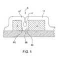
- FIG. 1illustrates the possible consequences of material layer deposition in a high aspect ratio feature 6 formed on a substrate 1 .
- the high aspect ratio feature 6may be any opening such as a space formed between adjacent features 2 , a contact, a via, or a trench defined in a material layer.
- a material layer 11that is formed using conventional deposition techniques (e.g., chemical vapor deposition (CVD) and/or physical vapor deposition (PVD)) tends to be deposited on the top edges 6 T of the feature 6 at a higher rate than at the bottom 6 B or sides 6 S thereof creating an overhang.
- This overhang or excess deposition of materialis sometimes referred to as crowning.
- Such excess materialcontinues to build up on the top edges 6 T of the feature 6 , until the opening is closed off by the deposited material 11 , forming a void 4 therein.
- the presence of voidsmay result in unreliable integrated circuit performance.
- the integrated barrier layercomprises at least a first refractory metal layer and a second refractory metal layer.
- the integrated barrier layeris formed using a dual-mode deposition process comprising a chemical vapor deposition (CVD) step and a cyclical deposition step.
- the dual-mode deposition processmay be performed in a single process chamber.
- the apparatusincludes a process chamber having a gas distribution plate therein.
- the gas distribution plateis configured to include two distribution zones for providing process gases to the chamber for both the chemical vapor deposition (CVD) process and the cyclical deposition process.
- a first distribution zonecomprises a center opening through which process gases for the cyclical deposition process are provided to the process chamber.
- a second distribution zonecomprises a plurality of openings radially dispersed around the center opening. The first distribution zone and the second distribution zone are isolated from one another to inhibit mixing of the process gases.
- a substrateis provided to the process chamber.
- a first refractory metal layermay be formed on the substrate using a chemical vapor deposition (CVD) process.
- a second refractory metal layermay be formed on the first refractory metal layer using a cyclical deposition process.
- Each of the first and second refractory metal layersmay comprise a different refractory metal.
- the integrated barrier layermay comprise a titanium nitride (TiN) layer formed using a chemical vapor deposition (CVD) process and a tungsten (W) layer formed on the titanium nitride (TiN) layer using a cyclical deposition process.
- the integrated barrier layeris compatible with integrated circuit fabrication processes.
- the integrated barrier layermay be used in a copper (Cu) interconnect structure.
- a preferred process sequenceincludes providing a substrate having an interconnect pattern defined in a dielectric material layer.
- An integrated barrier layercomprising a first refractory metal layer formed with a chemical vapor deposition (CVD) process and a second refractory metal layer formed with a cyclical deposition process is deposited on the interconnect pattern defined in the dielectric material using a single process chamber. Thereafter, the interconnect structure is completed by filling the interconnect pattern defined in the dielectric material with copper (Cu).
- CVDchemical vapor deposition
- the integrated barrier layermay be used as a diffusion barrier for gate electrodes.
- a preferred process sequenceincludes providing a substrate having gate regions formed on the surface thereof. The gate regions are surrounded by a dielectric material.
- An integrated barrier layercomprising a first refractory metal layer formed with a chemical vapor deposition (CVD) process and a second refractory metal layer formed with a cyclical deposition process is deposited on the gate regions using a single process chamber. Thereafter, the gate electrodes are completed by depositing a gate metal layer on the integrated barrier layer.
- CVDchemical vapor deposition
- the integrated barrier layermay also be used as a diffusion barrier for one or more electrodes of three-dimensional capacitor structures such as for example, trench capacitors and crown capacitors.
- a preferred process sequenceincludes providing a substrate having trenches defined therein.
- the trenchesinclude a first electrode and a dielectric material conformably formed along the sidewalls of the trenches.
- An integrated barrier layercomprising a first refractory metal layer formed with a chemical vapor deposition (CVD) process and a second refractory metal layer formed with a cyclical deposition process is deposited on the dielectric material in the trenches using a single process chamber. Thereafter, the trench capacitor structure is completed by depositing a second electrode on the integrated barrier layer.
- CVDchemical vapor deposition
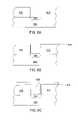
- FIG. 1is a cross-sectional view of one possible deposition result for high aspect ratio features filled using conventional prior art deposition techniques
- FIGS. 2A-2Bdepicts a schematic cross-sectional view of a process chamber and a top view of a gas distribution plate that can be used for the practice of embodiments described herein;
- FIG. 3is a block diagram of a gas delivery system for the gas distribution plate shown in FIG. 2B ;
- FIG. 4illustrates a process sequence for integrated barrier layer formation
- FIG. 5illustrates a process sequence for material layer formation using cyclical deposition techniques according to one embodiment described herein;
- FIG. 6illustrates a process sequence for material layer formation using cyclical deposition techniques according to an alternate embodiment described herein;
- FIGS. 7A-7Cillustrate schematic cross-sectional views of a substrate at different stages of an interconnect fabrication sequence
- FIGS. 8A-8Cillustrate schematic cross-sectional views of a substrate at different stages of a gate electrode fabrication sequence
- FIGS. 9A-9Dillustrate schematic cross-sectional views of a substrate at different stages of a trench capacitor fabrication sequence
- FIGS. 10A-10Bdepict cross-sectional views of a substrate at different stages of a crown capacitor fabrication sequence.
- FIG. 2Adepicts a schematic cross-sectional view of a process chamber 10 that can be used to perform deposition processes in accordance with embodiments described herein.
- the process chamber 10generally houses a wafer support pedestal 48 , which is used to support a substrate (not shown).
- the wafer support pedestal 48is movable in a vertical direction inside the process chamber 10 using a displacement mechanism 48 a.
- the substratecan be heated to some desired temperature prior to or during deposition.
- the wafer support pedestal 48may be heated using an embedded heater element 52 a.
- the wafer support pedestal 48may be resistively heated by applying an electric current from an AC power supply 52 to the heater element 52 a.
- the substrate(not shown) is, in turn, heated by the pedestal 48 .
- the wafer support pedestal 48may be heated using radiant heaters such as, for example, lamps (not shown).
- a temperature sensor 50 asuch as a thermocouple, is also embedded in the wafer support pedestal 48 to monitor the temperature of the pedestal 48 in a conventional manner. The measured temperature is used in a feedback loop to control the AC power supply 52 for the heating element 52 a , such that the substrate temperature can be maintained or controlled at a desired temperature which is suitable for the particular process application.
- a vacuum pump 18is used to evacuate the process chamber 10 and to maintain the pressure inside the process chamber 10 .
- a gas manifold 34through which process gases are introduced into the process chamber 10 , is located above the wafer support pedestal 48 .
- the gas manifold 34is coupled to a gas panel 51 , which controls and supplies various process gases to the process chamber 10 .
- gas manifold 34Proper control and regulation of the gas flows to the gas manifold 34 are performed by mass flow controllers (not shown) and a microprocessor controller 70 . Additionally, the gas manifold 34 may optionally be heated to prevent condensation of the reactive gases within the manifold.
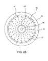
- the gas manifold 34includes a gas distribution plate 35 .
- the gas distribution plate 35is configured to include two gas distribution zones 42 , 45 for providing process gases to the process chamber for either a chemical vapor deposition (CVD) process or a cyclical deposition process.
- a first gas distribution zone 45comprises a center opening 36 through which process gases for the cyclical deposition process are provided to the process chamber.
- a second gas distribution zone 42comprises a plurality of openings 37 radially dispersed around the center opening 36 .
- the first gas distribution zone 45 and the second gas distribution zone 42are isolated from one another using one or more seals 38 , 47 which inhibit mixing of the process gases provided thereto.
- the one or more seals 38 , 47may comprise any suitable material that is non-reactive with the process gases provided to the process chamber, such as, for example, an o-ring.
- FIG. 3depicts a gas distribution system 50 that may be used to provide process gases to the gas distribution plate 35 ( FIG. 2A ).
- the gas distribution system 50includes process gas supplies 53 , 55 , 57 , 59 , purge gas supplies 85 , 86 , electronic control valves 60 , 61 , mass flow controllers (MFC) 64 , 65 , gas splitters 81 , 82 , a three-position valve 75 and a premix chamber 80 .
- MFCmass flow controllers
- a process gas from supplies 57 , 59is provided to electronic control valves 60 , 61 , respectively.
- a purge gas from the purge gas supply 85may be mixed with the process gases through gas splitters 81 , 82 .
- the electronic control valves 60 , 61 as used hereinrefer to any control valve capable of providing rapid and precise gas flow to the process chamber 10 with valve open and close cycles of less than about 1-2 seconds, and more preferably less than about 0.1 second.
- the electronic control valves 60 , 61are coupled to the center opening 36 in the first gas distribution zone 45 , via three-position valve 75 and gas line 88 .
- process gases from gas supplies 53 , 55are coupled through mass flow controllers (MFC) 64 , 65 , respectively, to premix chamber 80 .
- MFCmass flow controllers
- a purge gas from purge gas supply 86may also be provided to the premix chamber 80 .
- the process gasesare caused to mix. Generally, these gases are reactants that will react when they are exposed to a heated substrate.
- the mixed gasesare provided from the premix chamber 80 to the plurality of openings 37 in the second gas distribution zone 42 via gas line 87 .
- the microprocessor controller 70may be one of any form of general purpose computer processor (CPU) 71 that can be used in an industrial setting for controlling various chambers and sub-processors.
- the computermay use any suitable memory 72 , such as random access memory, read only memory, floppy disk drive, hard disk, or any other form of digital storage, local or remote.
- Various support circuits 73may be coupled to the CPU for supporting the processor in a conventional manner.
- Software routines as requiredmay be stored in the memory or executed by a second CPU that is remotely located.
- the software routinesare executed to initiate process recipes or sequences.
- the software routineswhen executed, transform the general purpose computer into a specific process computer that controls the chamber operation so that a chamber process is performed.
- software routinesmay be used to precisely control the activation of the electronic control valves for the execution of process sequences according to embodiments described herein.
- the software routinesmay be performed in hardware, as an application specific integrated circuit or other type of hardware implementation, or a combination of software and hardware.
- a dual-mode deposition process for forming an integrated barrier layer structure on a substrateis described.
- the dual-mode deposition processis performed in a single deposition chamber and comprises a chemical vapor deposition (CVD) step as well as a cyclical deposition step.
- CVDchemical vapor deposition
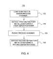
- FIG. 4illustrates an embodiment of the dual-mode deposition process sequence 100 detailing the various steps used for the formation of the integrated barrier layer structure.
- the integrated barrier layercomprises at least a first refractory metal layer and a second refractory metal layer.
- the dual-mode deposition processmay be performed in a process chamber similar to that described above with respect to FIGS. 2-3 .
- a substrateis provided to the process chamber.
- the substratemay be for example, a silicon substrate having gate regions formed thereon.
- a first refractory metal layeris formed on the substrate using a first deposition mode.
- the first deposition modemay comprise, for example, a chemical vapor deposition process wherein a refractory metal-containing precursor is thermally decomposed.
- the first refractory metal layermay comprise for example titanium (Ti), titanium nitride (TiN), tantalum (Ta), or tantalum nitride (TaN), among others.
- Suitable titanium-containing precursors for a CVD processmay include, for example, titanium tetrachloride (TiCl 4 ), tetrakis(dimethylamido)titanium (TDMAT) and tetrakis(diethylamido)titanium (TDEAT), among others.
- Suitable tantalum-containing precursors for a CVD processmay include, for example, pentakis(dimethylamido) tantalum (PDMAT), pentakis (ethylmethylamido) tantalum (PEMAT), tertbutylimidotris(diethylamido)tantalum (TBTDET), and pentakis(diethylamido)tantalum (PDEAT), among others.
- PDMATpentakis(dimethylamido) tantalum
- PEMATpentakis (ethylmethylamido) tantalum
- TBTDETtertbutylimidotris(diethylamido)tantalum
- PDEATpentakis(diethylamido)tantalum
- One exemplary process of depositing a titanium nitride (TiN) layer using a chemical vapor deposition (CVD) processcomprises thermally decomposing a titanium-containing precursor such as, for example, tetrakis (dimethylamido)titanium (TDMAT).
- TDMATtetrakis (dimethylamido)titanium
- the tetrakis(dimethylamido)titanium (TDMAT)may be provided to radially dispersed openings 37 ( FIG. 2B ) of the distribution plate 35 ( FIG. 2B ) in the process chamber at a flow rate between about 20 sccm to about 200 sccm, preferably between about 50 sccm to about 100 sccm.
- a carrier gas comprising helium (He)may be provided along with the tetrakis(dimethylamido)titanium (TDMAT) at a flow rate between about 500 sccm to about 2000 sccm, preferably between about 1000 sccm to about 1500 sccm.
- the substratemay be maintained at a temperature between about 200° C. to about 400° C., preferably between about 300° C. to about 350° C., at a chamber pressure between about 5 torr to about 15 torr, preferably about 10 torr.
- the process chamberis purged to remove any process gases remaining therein. Suitable purge gases may include argon (Ar), helium (He) and nitrogen (N 2 ). Thereafter, a second refractory metal layer is formed on the first refractory metal layer using a second deposition mode, as indicated in step 108 .
- the second refractory metal layermay be formed using a cyclical deposition process by alternately adsorbing a refractory metal-containing precursor and a reducing gas on the substrate.
- FIG. 5illustrates an embodiment of a cyclical deposition process sequence 200 according to the present invention detailing the various steps used for the deposition of the second refractory metal layer.
- the process chamber conditionssuch as, for example, the temperature and pressure are adjusted to enhance the adsorption of the process gases on the substrate.
- a carrier gas streamis established within the process chamber through the center opening 36 ( FIG. 2B ) in the gas distribution plate 35 ( FIG. 2B ), as indicated in step 204 .
- Carrier gasesmay be selected so as to also act as a purge gas for removal of volatile reactants and/or by-products from the process chamber.
- Carrier gasessuch as, for example, helium (He), argon (Ar), nitrogen (N 2 ) and hydrogen (H 2 ), and combinations thereof, among others may be used.
- a pulse of a refractory metal-containing precursoris added to the carrier gas stream.
- the term pulse as used hereinrefers to a dose of material injected into the process chamber or into the carrier gas stream.
- the pulse of the refractory metal-containing precursorlasts for a predetermined time interval.
- the second refractory metal layermay comprise for example, tungsten (W), tungsten nitride (WN), or tungsten boride (W 2 B), among others.
- Suitable tungsten-containing precursorsmay include, for example, tungsten hexafluoride (WF 6 ) and tungsten carbonyl (W(CO) 6 ), among others
- the time interval for the pulse of the refractory metal-containing precursoris variable depending on a number of factors such as, for example, the volume capacity of the process chamber employed, the vacuum system coupled thereto and the volatility/reactivity of the reactants used. For example, (1) a large-volume process chamber may lead to a longer time to stabilize the process conditions such as, for example, carrier purge gas flow and temperature, requiring a longer pulse time; and (2) a lower flow rate for the process gas may also lead to a longer time to stabilize the process conditions requiring a longer pulse time.
- the process conditionsare advantageously selected so that a pulse of the refractory metal-containing precursor provides a sufficient amount of precursor, such that at least a monolayer of the refractory metal-containing precursor is adsorbed on the substrate. Thereafter, excess refractory metal-containing precursor remaining in the chamber may be removed from the process chamber by the carrier gas stream in combination with the vacuum system.
- step 208after the excess refractory metal-containing precursor has been sufficiently removed from the process chamber by the carrier gas stream to prevent co-reaction or particle formation with a subsequently provided process gas, a pulse of a reducing gas is added to the carrier gas stream.
- Suitable reducing gasesmay include for example, silane (SiH 4 ), disilane (Si 2 H 6 ), dichlorosilane (SiCl 2 H 2 ), ammonia (NH 3 ), hydrazine (N 2 H 4 ), monomethyl hydrazine (CH 3 N 2 H 3 ), dimethyl hydrazine (C 2 H 6 N 2 H 2 ), t-butyl hydrazine (C 4 H 9 N 2 H 3 ), phenyl hydrazine (C 6 H 5 N 2 H 3 ), 2,2′-azoisobutane ((CH 3 ) 6 C 2 N 2 ), ethylazide (C 2 H 5 N 3 ), borane (BH 3 ), diborane (B 2 H 6 ), triborane (B 3 H 9 ), tetraborane (B 4 H 12 ), pentaborane (B 5 H 15 ), hexaborane (B 6 H 18 ), heptabo
- the pulse of the reducing gasalso lasts for a predetermined time interval.
- the time interval for the pulse of the reducing gasshould be long enough to provide a sufficient amount of the reducing gas for reaction with the refractory metal-containing precursor that is already adsorbed on the substrate. Thereafter, excess reducing gas is flushed from the process chamber by the carrier gas stream in combination with the vacuum system.
- Steps 204 through 208comprise one embodiment of a deposition cycle for the second refractory metal-containing layer.
- a constant flow of the carrier gasis provided to the process chamber modulated by alternating periods of pulsing and non-pulsing where the periods of pulsing alternate between the refractory metal-containing precursor and the reducing gas along with the carrier gas stream, while the periods of non-pulsing include only the carrier gas stream.
- the time interval for each of the pulses of the refractory metal-containing precursor and the reducing gasmay have the same duration. That is the duration of the pulse of the refractory metal-containing precursor may be identical to the duration of the pulse of the reducing gas.
- a time interval (T 1 ) for the pulse of the refractory metal-containing precursorequals a time interval (T 2 ) for the pulse of the reducing gas.
- the time interval for each of the pulses of the refractory metal-containing precursor and the reducing gasmay have different durations. That is the duration of the pulse of the refractory metal-containing precursor may be shorter or longer than the duration of the pulse of the reducing gas.
- a time interval (T 1 ) for the pulse of the refractory metal-containing precursoris different than a time interval (T 2 ) for the pulse of the reducing gas.
- the periods of non-pulsing between each of the pulses of the refractory metal-containing precursor and the reducing gasmay have the same duration. That is, the duration of the period of non-pulsing between each pulse of the refractory metal-containing precursor and each pulse of the reducing gas is identical.
- a time interval (T 3 ) of non-pulsing between the pulse of the refractory metal-containing precursor and the pulse of the reducing gasequals a time interval (T 4 ) of non-pulsing between the pulse of the reducing gas and the pulse of the refractory metal-containing precursor.
- the periods of non-pulsing between each of the pulses of the refractory metal-containing precursor and the reducing gasmay have different durations. That is, the duration of the period of non-pulsing between each pulse of the refractory metal-containing precursor and each pulse of the reducing gas may be shorter or longer than the duration of the period of non-pulsing between each pulse of the reducing gas and the pulse of the refractory metal-containing precursor.
- a time interval (T 3 ) of non-pulsing between the pulse of the refractory metal-containing precursor and the pulse of the reducing gasis different from a time interval (T 4 ) of non-pulsing between the pulse of the reducing gas and the pulse of the refractory metal-containing precursor.
- T 3a time interval of non-pulsing between the pulse of the refractory metal-containing precursor and the pulse of the reducing gas
- T 4time interval
- time intervals for each pulse of the refractory metal-containing precursor, the reducing gas and the periods of non-pulsing therebetween for each deposition cyclemay have the same duration.
- a time interval (T 1 ) for the pulse of the refractory metal-containing precursorhas the same duration as the time interval (T 1 ) for the pulse of the refractory metal-containing precursor in subsequent deposition cycles (C 2 . . . C N ).
- the duration of each pulse of the reducing gas as well as the periods of non-pulsing between the pulse of the refractory metal-containing precursor and the reducing gas in the first deposition cycle (C 1 )is the same as the duration of each pulse of the reducing gas and the periods of non-pulsing between the pulse of the refractory metal-containing precursor and the reducing gas in subsequent deposition cycles (C 2 . . . C N ), respectively.
- the time intervals for at least one pulse of the refractory metal-containing precursor, the reducing gas and the periods of non-pulsing therebetween for one or more of the deposition cycles of the second refractory metal layermay have different durations.
- one or more of the time intervals (T 1 ) for the refractory metal-containing precursor, the time intervals (T 2 ) for the reducing gas, the time intervals (T 3 ) of non-pulsing between the pulse of the refractory metal-containing precursor and the pulse of the reducing gas and the time interval (T 4 ) of non-pulsing between the pulse of the reducing gas and the pulse of the refractory metal-containing precursormay have different values for one or more subsequent deposition cycles of the cyclical deposition process.
- the time interval (T 1 ) for the pulse of the refractory metal-containing precursormay be longer or shorter than the time interval (T 1 ) for the pulse of the refractory metal-containing precursor in subsequent deposition cycles (C 2 . . . C N ).
- the duration of each pulse of the reducing gas and the periods of non-pulsing between the pulse of the refractory metal-containing precursor and the reducing gas in deposition cycle (C 1 )may be the same or different than the duration of corresponding pulses of the reducing gas and the periods of non-pulsing between the pulse of the refractory metal-containing precursor and the reducing gas in subsequent deposition cycles (C 2 . . . C N ), respectively.
- step 210after each deposition cycle (steps 204 through 208 ) a total thickness of the second refractory metal will be formed on the substrate. Depending on specific device requirements, subsequent deposition cycles may be needed to achieve a desired thickness. As such, steps 204 through 208 are repeated until the desired thickness for the second refractory metal layer is achieved. Thereafter, when the desired thickness for the second refractory metal layer is achieved the process is stopped as indicated by step 212 .
- a refractory metal layer deposition sequence 300includes adjusting the process chamber conditions (step 302 ), providing a first pulse of a purge gas to the process chamber (step 304 ), providing a pulse of a refractory metal-containing precursor to the process chamber (step 306 ), providing a second pulse of a purge gas to the process chamber (step 308 ), providing a pulse of the reducing gas to the process chamber (step 310 ), and then repeating steps 304 through 308 , or stopping the deposition process (step 314 ) depending on whether a desired thickness for the refractory metal layer has been achieved (step 312 ).
- the time intervals for each of the pulses of the refractory metal-containing precursor, the reducing gas and the purge gasmay have the same or different durations as discussed above with respect to FIG. 5 .
- corresponding time intervals for one or more pulses of the refractory metal-containing precursor, the reducing gas and the purge gas in one or more of the deposition cycles of the refractory metal layer deposition processmay have different durations.
- the refractory metal layer deposition cycleis depicted as beginning with a pulse of the refractory metal-containing precursor followed by a pulse of the reducing gas.
- the refractory metal layer deposition cyclemay start with a pulse of the reducing gas followed by a pulse of the refractory metal-containing precursor.
- One exemplary process of depositing a tungsten layercomprises sequentially providing pulses of tungsten hexafluoride (WF 6 ) and pulses of diborane (B 2 H 6 ).
- the tungsten hexafluoride (WF 6 )may be provided to an appropriate flow control valve, for example, an electronic control valve, at a flow rate of between about 10 sccm (standard cubic centimeters per minute) and about 400 sccm, preferably between about 20 sccm and about 100 sccm, and thereafter pulsed for about 1 second or less, preferably about 0.2 seconds or less.
- a carrier gas comprising argon (Ar)is provided along with the tungsten hexaflouride (WF 6 ) at a flow rate between about 250 sccm to about 1000 sccm, preferably between about 500 sccm to about 750 sccm.
- the diborane (B 2 H 6 )may be provided to an appropriate flow control valve, for example, an electronic control valve, at a flow rate of between about 5 sccm and about 150 sccm, preferably between about 5 sccm and about 25 sccm, and thereafter pulsed for about 1 second or less, preferably about 0.2 seconds or less.
- a carrier gas comprising argon (Ar)is provided along with the diborane (B 2 H 6 ) at a flow rate between about 250 sccm to about 1000 sccm, preferably between about 500 sccm to about 750 sccm.
- the substratemay be maintained at a temperature between about 250° C. and about 350° C., preferably about 300° C. at a chamber pressure between about 1 torr to about 10 torr, preferably about 5 torr.
- Another exemplary process of depositing a tungsten layercomprises sequentially providing pulses of tungsten hexaflouride (WF 6 ) and pulses of silane (SiH 4 ).
- the tungsten hexafluoride (WF 6 )may be provided to an appropriate flow control valve, for example, an electronic control valve, at a flow rate of between about 10 sccm (standard cubic centimeters per minute) and about 400 sccm, preferably between about 20 sccm and about 100 sccm, and thereafter pulsed for about 1 second or less, preferably about 0.2 seconds or less.
- a carrier gas comprising argon (Ar)is provided to along with the tungsten hexaflouride (WF 6 ) at a flow rate between about 250 sccm to about 1000 sccm, preferably between about 300 sccm to about 500 sccm.
- the silane (SiH 4 )may be provided to an appropriate flow control valve, for example, an electronic control valve, at a flow rate between about 10 sccm to about 500 sccm, preferably between about 50 sccm to about 200 sccm, and thereafter pulsed for about 1 second or less, preferably about 0.2 seconds or less.
- a carrier gas comprising argon (Ar)is provided along with the silane (SiH 4 ) at a flow rate between about 250 sccm to about 1000 sccm, preferably between about 300 sccm to about 500 sccm.
- a pulse of a purge gas comprising argon (Ar) at a flow rate between about 300 sccm to about 1000 sccm, preferably between about 500 sccm to about 750 sccm, in pulses of about 1 second or less, preferably about 0.3 seconds or lessis provided between the pulses of the tungsten hexafluoride (WF 6 ) and the pulses of silane (SiH 4 ).
- the substratemay be maintained at a temperature between about 300° C. to about 400° C., preferably about 350° C., at a chamber pressure between about 1 torr to about 10 torr.
- the dual-mode deposition processis depicted as forming the first refractory metal layer using a chemical vapor deposition (CVD) process followed by formation of the second refractory metal layer using a cyclical deposition process.
- the dual-mode deposition processmay start with a first refractory metal layer deposited using a cyclical deposition process followed by a second refractory metal layer deposited using a chemical vapor deposition (CVD) process.
- FIGS. 7A-7Cillustrate cross-sectional views of a substrate at different stages of a copper interconnect fabrication sequence incorporating the integrated barrier layer of the present invention.
- FIG. 7Aillustrates a cross-sectional view of a substrate 400 having metal contacts 404 and a dielectric layer 402 formed thereon.
- the substrate 400may comprise a semiconductor material such as, for example, silicon (Si), germanium (Ge), or gallium arsenide (GaAs).
- the dielectric layer 402may comprise an insulating material such as, for example, silicon oxide or silicon nitride.
- the metal contacts 404may comprise for example, copper (Cu).
- Apertures 404 Hmay be defined in the dielectric layer 402 to provide openings over the metal contacts 404 .
- the apertures 404 Hmay be defined in the dielectric layer 402 using conventional lithography and etching techniques.
- an integrated barrier layer 406is formed in the apertures 404 H defined in the dielectric layer 402 .
- the integrated barrier layer 406comprises a titanium nitride (TiN) layer formed with a chemical vapor deposition (CVD) process and a tungsten (W) layer formed with a cyclical deposition process.
- TiNtitanium nitride
- CVDchemical vapor deposition
- Wtungsten
- the integrated barrier layer 406is formed using the deposition techniques described above with respect to FIGS. 4-6 .
- the thickness of the integrated barrier layer 406is typically about 20 ⁇ to about 500 ⁇ .
- the apertures 404 Hare filled with copper (Cu) metallization 408 using a suitable deposition process as shown in FIG. 7C .
- copper (Cu)may be deposited with a chemical vapor deposition (CVD) process using copper-containing precursors such as Cu +2 (hfac) 2 (copper hexafluoro acetylacetonate), Cu +2 (fod) 2 (copper heptafluoro dimethyl octanediene), Cu +1 hfac TMVS (copper hexafluoro acetylacetonate trimethylvinylsilane), among others.
- CVDchemical vapor deposition
- FIGS. 8A-8Cillustrate cross-sectional views of a substrate at different stages of a gate electrode fabrication sequence incorporating the integrated barrier layer of the present invention.
- FIG. 8Aillustrates a cross-sectional view of a substrate 500 having gate regions 504 formed on the surface thereof. The gate regions 504 are surrounded by a dielectric material 502 .
- the substrate 500may comprise a semiconductor material such as, for example, silicon (Si), germanium (Ge), or gallium arsenide (GaAs).
- the dielectric material 502may comprise an insulating material such as, for example, silicon oxide or silicon nitride.
- an integrated barrier layer 506is formed on the gate regions 504 .
- the integrated barrier layer 506comprises a titanium nitride (TiN) layer formed with a chemical vapor deposition (CVD) process and a tungsten (W) layer formed with a cyclical deposition process.
- TiNtitanium nitride
- CVDchemical vapor deposition
- Wtungsten
- the integrated barrier layer 506is formed using the deposition techniques described above with respect to FIGS. 4-6 .
- the thickness of the integrated barrier layer 506is typically about 20 ⁇ to about 500 ⁇ .
- the gate metallizationmay comprise tungsten (W), aluminum (Al) or copper (Cu), among others.
- tungsten (W)may be deposited with a chemical vapor deposition (CVD) process from the thermal decomposition of tungsten hexafluoride (WF 6 ) or tungsten carbonyl (W(CO) 6 ); aluminum may be deposited with a chemical vapor deposition (CVD) process using dimethyl aluminum hydride (DMAH); or copper (Cu) may be deposited with a chemical vapor deposition (CVD) process using copper-containing precursors such as Cu +2 (hfac) 2 (copper hexafluoro acetylacetonate), Cu +2 (fod) 2 (copper heptafluoro dimethyl octanediene), or Cu +1 hfac TMVS (
- FIGS. 9A-9Dare illustrative of a metal-insulator-metal (MIM) trench capacitor fabrication sequence incorporating the integrated barrier layer of the present invention.
- FIG. 9Aillustrates a cross-sectional view of a substrate 655 having a dielectric material layer 657 formed thereon.
- the substrate 655may comprise a semiconductor material such as, for example, silicon (Si), germanium (Ge), or gallium arsenide (GaAs).
- the dielectric material layer 657may comprise an insulator such as, for example, silicon oxide or silicon nitride.
- At least one trench 659is defined in the dielectric material layer 657 .
- the trenchmay be formed using conventional lithography and etching techniques.
- a first integrated barrier layer 660is formed on the trench 659 .
- the first integrated barrier layer 660comprises a titanium nitride (TiN) layer formed with a chemical vapor deposition (CVD) process and a tungsten (W) layer formed with a cyclical deposition process.
- TiNtitanium nitride
- CVDchemical vapor deposition
- Wtungsten
- the first integrated barrier layer 660is formed using the deposition techniques described above with respect to FIGS. 4-6 .
- the thickness of the integrated barrier layer 660is typically about 20 ⁇ to about 500 ⁇ .
- a first metal layer 661is formed over the first integrated barrier layer 660 .
- the first metal layer 661comprises the first electrode of the metal-insulator-metal (MIM) trench capacitor.
- a suitable metal for the first metal layer 661includes, for example, tungsten (W).
- the thickness of the first metal layer 661is typically about 100 ⁇ to about 1000 ⁇ .
- the trench capacitorfurther includes an insulating layer 663 formed over the metal layer 661 , as shown in FIG. 9C .
- the insulating layer 663preferably comprises a high dielectric constant material (dielectric constant greater then about 10).
- High dielectric constant materialsadvantageously permit higher charge storage capacities for the capacitor structures.
- Suitable dielectric materialsmay include for example, tantalum pentoxide (Ta 2 O 5 ), silicon oxide/silicon nitride/oxynitride (ONO), aluminum oxide (Al 2 O 3 ), barium strontium titanate (BST), barium titanate, lead zirconate titanate (PZT), lead lanthanium titanate, strontium titanate and strontium bismuth titanate, among others.
- the thickness of the insulating layer 663is variable depending on the dielectric constant of the material used and the geometry of the device being fabricated. Typically, the insulating layer 663 has a thickness of about 100 ⁇ to about 1000 ⁇ .
- a second integrated barrier layer 664is formed on the insulating layer 663 .
- the second integrated barrier layer 664comprises a titanium nitride (TiN) layer formed with a chemical vapor deposition (CVD) process and a tungsten (W) layer formed with a cyclical deposition process.
- TiNtitanium nitride
- CVDchemical vapor deposition
- Wtungsten
- the second integrated barrier layer 664is formed using the deposition techniques described above with respect to FIGS. 4-6 .
- the thickness of the integrated barrier layer 664is typically about 20 ⁇ to about 500 ⁇ .
- a second metal layer 665is formed over the second integrated barrier layer 664 .
- the second metal layer 665comprises the second electrode of the metal-insulator-metal (MIM) trench capacitor.
- a suitable metal for the second metal layer 665includes, for example, tungsten (W).
- the thickness of the second metal layer 665is typically about 100 ⁇ to about 1000 ⁇ .
- the metal-insulator-metal (MIM) trench capacitoris completed by filling the trench 659 with, for example, a polysilicon layer 667 , as shown in FIG. 9D .
- the polysilicon layer 667may be formed using conventional deposition techniques.
- the polysilicon layer 667may be deposited using a chemical vapor deposition (CVD) process in which silane (SiH 4 ) is thermally decomposed to form polysilicon at a temperature between about 550° C. and 700° C.
- CVDchemical vapor deposition
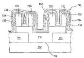
- FIGS. 10A-10Billustrate cross-sectional views of a substrate at different stages of a crown capacitor fabrication sequence incorporating the integrated barrier layer of the present invention.
- the term crown capacitor as used hereinrefers to a capacitor structure having a three-dimensional shape formed above the surface of the substrate. The three-dimensional shape increases the capacitance of the device by increasing the surface area thereof.
- FIG. 10Aillustrates a cross-sectional view of a substrate 712 having a dielectric layer 714 formed thereon.
- the substrate 712may comprise a semiconductor material such as, for example, silicon (Si), germanium (Ge), or gallium arsenide (GaAs).
- the dielectric 714may comprise an oxide such as, for example, a silicon oxide.
- the dielectric layer 714has at least one aperture 716 formed therein.
- a first polysilicon layer 718is formed over the dielectric layer 714 and the at least one aperture 716 .
- the first polysilicon layer 718may be doped with a suitable dopant such as, for example, arsenic (As), antimony (Sb), phosphorous (P) and boron (B), among others.
- a hemispherical silicon grain layer (HSG) 720 or a rough polysilicon layermay optionally be formed over the first polysilicon layer 718 to increase the surface area thereof.
- the hemispherical silicon grain layer 720may be formed, for example, by depositing an amorphous silicon layer and than annealing it to form a rough surface thereon.
- the hemispherical silicon grain layer 720may optionally by doped.
- the first polysilicon layer 718 and the hemispherical silicon grain layer (HSG) 720are patterned and etched to form a crown structure 730 . Both the first polysilicon layer 718 and the hemispherical silicon grain layer (HSG) act as a first electrode for the crown capacitor.
- the crown capacitorfurther includes an insulating layer 732 formed over the hemispherical silicon grain layer 718 of the crown structure 730 .
- the insulating layer 732preferably comprises a high dielectric constant material (dielectric constant greater then about 10).
- High dielectric constant materialsadvantageously permit higher charge storage capacities for the capacitor structures.
- Suitable dielectric materialsmay include for example, tantalum pentoxide (Ta 2 O 5 ), silicon oxide/silicon nitride/oxynitride (ONO), aluminum oxide (Al 2 O 3 ), barium strontium titanate (BST), barium titanate, lead zirconate titanate (PZT), lead lanthanium titanate, strontium titanate and strontium bismuth titanate, among others.
- an integrated barrier layer 734is formed on the insulating layer 732 .
- the integrated barrier layer 734comprises a titanium nitride (TiN) layer formed with a chemical vapor deposition (CVD) process and a tungsten (W) layer formed with a cyclical deposition process.
- TiNtitanium nitride
- CVDchemical vapor deposition
- Wtungsten
- the integrated barrier layer 734is formed using the deposition techniques described above with respect to FIGS. 4-6 .
- the thickness of the integrated barrier layer 734is typically about 20 ⁇ to about 500 ⁇ .
- a metal layer 742is formed over the integrated barrier layer 734 .
- the metal layer 742comprises the second electrode of the crown capacitor.
- a suitable metal for the metal layer 742includes, for example, tungsten (W).
- the thickness of the metal layer 742is typically about 100 ⁇ to about 1000 ⁇ .
- the crown capacitoris completed by depositing, for example, a second polysilicon layer 752 thereover, as shown in FIG. 10B .
- the second polysilicon layer 752may be formed using conventional deposition techniques.
- the second polysilicon layer 752may be deposited using a chemical vapor deposition (CVD) process in which silane (SiH 4 ) is thermally decomposed to form polysilicon at a temperature between about 550° C. and 700° C.
- CVDchemical vapor deposition
Landscapes
- Engineering & Computer Science (AREA)
- Microelectronics & Electronic Packaging (AREA)
- Condensed Matter Physics & Semiconductors (AREA)
- General Physics & Mathematics (AREA)
- Manufacturing & Machinery (AREA)
- Computer Hardware Design (AREA)
- Physics & Mathematics (AREA)
- Power Engineering (AREA)
- Chemical & Material Sciences (AREA)
- Chemical Kinetics & Catalysis (AREA)
- General Chemical & Material Sciences (AREA)
- Electrodes Of Semiconductors (AREA)
- Internal Circuitry In Semiconductor Integrated Circuit Devices (AREA)
- Chemical Vapour Deposition (AREA)
Abstract
Description
This application claims the benefit of U.S. Provisional Application No. 60/386,221 filed Apr. 16, 2002, which is hereby incorporated by reference.
1. Field of the Invention
Embodiments of the present invention generally relate to a method of barrier layer formation and, more particularly to a method of integrated barrier layer formation using both cyclical deposition techniques and chemical vapor deposition techniques.
2. Description of the Background Art
In the manufacture of integrated circuits, contact level metallization schemes are often used to provide low resistance contacts to an underlying semiconductor material. Typically, contact level metallization schemes combine an integrated barrier layer with a contact level metal layer.
For example, when a gate electrode of a transistor is fabricated, an integrated barrier layer (e.g., titanium nitride/tungsten (TiN/W)) is formed between the gate material (e.g., polysilicon) and the contact level metal layer (e.g., aluminum (Al) or copper (Cu)) of the gate electrode. The integrated barrier layer inhibits the diffusion of the aluminum (Al) or copper (Cu) into the polysilicon gate material. Such aluminum (Al) or copper (Cu) diffusion is undesirable because it potentially changes the characteristics of the transistor, rendering the transistor inoperable.
The integrated barrier layer typically comprises two different material layers. Each of the material layers is typically formed using a separate process chamber. For example, separate deposition chambers may be used for depositing the titanium nitride (TiN) layer and the tungsten (W) layer comprising a titanium nitride/tungsten (TiN/W) integrated barrier layer. The separate deposition chambers may include, for example, physical vapor deposition (PVD) chambers and/or chemical vapor deposition (CVD) chambers. However, the use of separate deposition chambers to form each material layer comprising the integrated barrier layer is costly.
Additionally, as circuit densities increase, the widths of integrated circuit features such as, for example, gate electrodes, may decrease to sub-micron dimensions (e. g., less than 0.25 micrometers), whereas the thickness of material layers between such features typically remains substantially constant, increasing the aspect ratios therefor. The term aspect ratio as used herein refers to the ratio of the feature height divided by the feature width. Many traditional deposition processes have difficulty filling sub-micron features where the aspect ratio exceeds 8:1, and especially where the aspect ratio exceeds 10:1.
Therefore, a need exists for a system and method for forming integrated barrier layer structures.
An apparatus and method for forming an integrated barrier layer on a substrate is described. The integrated barrier layer comprises at least a first refractory metal layer and a second refractory metal layer. The integrated barrier layer is formed using a dual-mode deposition process comprising a chemical vapor deposition (CVD) step and a cyclical deposition step. The dual-mode deposition process may be performed in a single process chamber.
In one embodiment, the apparatus includes a process chamber having a gas distribution plate therein. The gas distribution plate is configured to include two distribution zones for providing process gases to the chamber for both the chemical vapor deposition (CVD) process and the cyclical deposition process. A first distribution zone comprises a center opening through which process gases for the cyclical deposition process are provided to the process chamber. A second distribution zone comprises a plurality of openings radially dispersed around the center opening. The first distribution zone and the second distribution zone are isolated from one another to inhibit mixing of the process gases.
In operation, a substrate is provided to the process chamber. A first refractory metal layer may be formed on the substrate using a chemical vapor deposition (CVD) process. Thereafter, a second refractory metal layer may be formed on the first refractory metal layer using a cyclical deposition process. Each of the first and second refractory metal layers may comprise a different refractory metal. For example, the integrated barrier layer may comprise a titanium nitride (TiN) layer formed using a chemical vapor deposition (CVD) process and a tungsten (W) layer formed on the titanium nitride (TiN) layer using a cyclical deposition process.
The integrated barrier layer is compatible with integrated circuit fabrication processes. In one integrated circuit fabrication process, the integrated barrier layer may be used in a copper (Cu) interconnect structure. For a copper (Cu) interconnect fabrication process, a preferred process sequence includes providing a substrate having an interconnect pattern defined in a dielectric material layer. An integrated barrier layer comprising a first refractory metal layer formed with a chemical vapor deposition (CVD) process and a second refractory metal layer formed with a cyclical deposition process is deposited on the interconnect pattern defined in the dielectric material using a single process chamber. Thereafter, the interconnect structure is completed by filling the interconnect pattern defined in the dielectric material with copper (Cu).
In another integrated circuit fabrication process, the integrated barrier layer may be used as a diffusion barrier for gate electrodes. For a gate electrode fabrication process, a preferred process sequence includes providing a substrate having gate regions formed on the surface thereof. The gate regions are surrounded by a dielectric material. An integrated barrier layer comprising a first refractory metal layer formed with a chemical vapor deposition (CVD) process and a second refractory metal layer formed with a cyclical deposition process is deposited on the gate regions using a single process chamber. Thereafter, the gate electrodes are completed by depositing a gate metal layer on the integrated barrier layer.
The integrated barrier layer may also be used as a diffusion barrier for one or more electrodes of three-dimensional capacitor structures such as for example, trench capacitors and crown capacitors. For a trench capacitor structure, a preferred process sequence includes providing a substrate having trenches defined therein. The trenches include a first electrode and a dielectric material conformably formed along the sidewalls of the trenches. An integrated barrier layer comprising a first refractory metal layer formed with a chemical vapor deposition (CVD) process and a second refractory metal layer formed with a cyclical deposition process is deposited on the dielectric material in the trenches using a single process chamber. Thereafter, the trench capacitor structure is completed by depositing a second electrode on the integrated barrier layer.
So that the manner in which the above recited features of the present invention are attained and can readily be understood in detail, a more particular description of the invention, briefly summarized above, may be had by reference to the embodiments thereof which are illustrated in the appended drawings.
It is to be noted, however, that the appended drawings illustrate only typical embodiments of the invention and are therefore not to be considered limiting of its scope, for the invention may admit to other equally effective embodiments.
Depending on the specific deposition process, the substrate can be heated to some desired temperature prior to or during deposition. For example, thewafer support pedestal 48 may be heated using an embeddedheater element 52a.Thewafer support pedestal 48 may be resistively heated by applying an electric current from anAC power supply 52 to theheater element 52a.The substrate (not shown) is, in turn, heated by thepedestal 48. Alternatively, thewafer support pedestal 48 may be heated using radiant heaters such as, for example, lamps (not shown).
Atemperature sensor 50a,such as a thermocouple, is also embedded in thewafer support pedestal 48 to monitor the temperature of thepedestal 48 in a conventional manner. The measured temperature is used in a feedback loop to control theAC power supply 52 for theheating element 52a, such that the substrate temperature can be maintained or controlled at a desired temperature which is suitable for the particular process application.
Avacuum pump 18 is used to evacuate theprocess chamber 10 and to maintain the pressure inside theprocess chamber 10. Agas manifold 34, through which process gases are introduced into theprocess chamber 10, is located above thewafer support pedestal 48. Thegas manifold 34 is coupled to agas panel 51, which controls and supplies various process gases to theprocess chamber 10.
Proper control and regulation of the gas flows to thegas manifold 34 are performed by mass flow controllers (not shown) and amicroprocessor controller 70. Additionally, thegas manifold 34 may optionally be heated to prevent condensation of the reactive gases within the manifold.
Thegas manifold 34 includes agas distribution plate 35. Referring toFIG. 2B , thegas distribution plate 35 is configured to include twogas distribution zones gas distribution zone 45 comprises acenter opening 36 through which process gases for the cyclical deposition process are provided to the process chamber. A secondgas distribution zone 42 comprises a plurality ofopenings 37 radially dispersed around thecenter opening 36.
The firstgas distribution zone 45 and the secondgas distribution zone 42 are isolated from one another using one ormore seals more seals
For the cyclical deposition mode, a process gas fromsupplies electronic control valves purge gas supply 85 may be mixed with the process gases throughgas splitters electronic control valves process chamber 10 with valve open and close cycles of less than about 1-2 seconds, and more preferably less than about 0.1 second. Theelectronic control valves gas distribution zone 45, via three-position valve 75 andgas line 88.
For the chemical vapor deposition (CVD) mode, process gases fromgas supplies chamber 80. A purge gas frompurge gas supply 86 may also be provided to thepremix chamber 80. In thepremix chamber 80, the process gases are caused to mix. Generally, these gases are reactants that will react when they are exposed to a heated substrate. The mixed gases are provided from thepremix chamber 80 to the plurality ofopenings 37 in the secondgas distribution zone 42 viagas line 87.
Themicroprocessor controller 70 may be one of any form of general purpose computer processor (CPU)71 that can be used in an industrial setting for controlling various chambers and sub-processors. The computer may use anysuitable memory 72, such as random access memory, read only memory, floppy disk drive, hard disk, or any other form of digital storage, local or remote.Various support circuits 73 may be coupled to the CPU for supporting the processor in a conventional manner. Software routines as required may be stored in the memory or executed by a second CPU that is remotely located.
The software routines are executed to initiate process recipes or sequences. The software routines, when executed, transform the general purpose computer into a specific process computer that controls the chamber operation so that a chamber process is performed. For example, software routines may be used to precisely control the activation of the electronic control valves for the execution of process sequences according to embodiments described herein. Alternatively, the software routines may be performed in hardware, as an application specific integrated circuit or other type of hardware implementation, or a combination of software and hardware.
Integrated Barrier Layer Formation
A dual-mode deposition process for forming an integrated barrier layer structure on a substrate is described. The dual-mode deposition process is performed in a single deposition chamber and comprises a chemical vapor deposition (CVD) step as well as a cyclical deposition step.
As indicated instep 102, a substrate is provided to the process chamber. The substrate may be for example, a silicon substrate having gate regions formed thereon. Referring to step104, a first refractory metal layer is formed on the substrate using a first deposition mode. The first deposition mode may comprise, for example, a chemical vapor deposition process wherein a refractory metal-containing precursor is thermally decomposed.
The first refractory metal layer may comprise for example titanium (Ti), titanium nitride (TiN), tantalum (Ta), or tantalum nitride (TaN), among others. Suitable titanium-containing precursors for a CVD process may include, for example, titanium tetrachloride (TiCl4), tetrakis(dimethylamido)titanium (TDMAT) and tetrakis(diethylamido)titanium (TDEAT), among others. Suitable tantalum-containing precursors for a CVD process may include, for example, pentakis(dimethylamido) tantalum (PDMAT), pentakis (ethylmethylamido) tantalum (PEMAT), tertbutylimidotris(diethylamido)tantalum (TBTDET), and pentakis(diethylamido)tantalum (PDEAT), among others.
One exemplary process of depositing a titanium nitride (TiN) layer using a chemical vapor deposition (CVD) process comprises thermally decomposing a titanium-containing precursor such as, for example, tetrakis (dimethylamido)titanium (TDMAT). The tetrakis(dimethylamido)titanium (TDMAT) may be provided to radially dispersed openings37 (FIG. 2B ) of the distribution plate35 (FIG. 2B ) in the process chamber at a flow rate between about 20 sccm to about 200 sccm, preferably between about 50 sccm to about 100 sccm. A carrier gas comprising helium (He) may be provided along with the tetrakis(dimethylamido)titanium (TDMAT) at a flow rate between about 500 sccm to about 2000 sccm, preferably between about 1000 sccm to about 1500 sccm. The substrate may be maintained at a temperature between about 200° C. to about 400° C., preferably between about 300° C. to about 350° C., at a chamber pressure between about 5 torr to about 15 torr, preferably about 10 torr.
Referring to step106, after the first refractory metal layer is formed on the substrate using a first deposition mode, the process chamber is purged to remove any process gases remaining therein. Suitable purge gases may include argon (Ar), helium (He) and nitrogen (N2). Thereafter, a second refractory metal layer is formed on the first refractory metal layer using a second deposition mode, as indicated instep 108. The second refractory metal layer may be formed using a cyclical deposition process by alternately adsorbing a refractory metal-containing precursor and a reducing gas on the substrate.
In one embodiment where a constant carrier gas flow is desired, a carrier gas stream is established within the process chamber through the center opening36 (FIG. 2B ) in the gas distribution plate35 (FIG. 2B ), as indicated instep 204. Carrier gases may be selected so as to also act as a purge gas for removal of volatile reactants and/or by-products from the process chamber. Carrier gases such as, for example, helium (He), argon (Ar), nitrogen (N2) and hydrogen (H2), and combinations thereof, among others may be used.
Referring to step206, after the carrier gas stream is established within the process chamber, a pulse of a refractory metal-containing precursor is added to the carrier gas stream. The term pulse as used herein refers to a dose of material injected into the process chamber or into the carrier gas stream. The pulse of the refractory metal-containing precursor lasts for a predetermined time interval.
The second refractory metal layer may comprise for example, tungsten (W), tungsten nitride (WN), or tungsten boride (W2B), among others. Suitable tungsten-containing precursors may include, for example, tungsten hexafluoride (WF6) and tungsten carbonyl (W(CO)6), among others
The time interval for the pulse of the refractory metal-containing precursor is variable depending on a number of factors such as, for example, the volume capacity of the process chamber employed, the vacuum system coupled thereto and the volatility/reactivity of the reactants used. For example, (1) a large-volume process chamber may lead to a longer time to stabilize the process conditions such as, for example, carrier purge gas flow and temperature, requiring a longer pulse time; and (2) a lower flow rate for the process gas may also lead to a longer time to stabilize the process conditions requiring a longer pulse time. In general, the process conditions are advantageously selected so that a pulse of the refractory metal-containing precursor provides a sufficient amount of precursor, such that at least a monolayer of the refractory metal-containing precursor is adsorbed on the substrate. Thereafter, excess refractory metal-containing precursor remaining in the chamber may be removed from the process chamber by the carrier gas stream in combination with the vacuum system.
Instep 208, after the excess refractory metal-containing precursor has been sufficiently removed from the process chamber by the carrier gas stream to prevent co-reaction or particle formation with a subsequently provided process gas, a pulse of a reducing gas is added to the carrier gas stream. Suitable reducing gases may include for example, silane (SiH4), disilane (Si2H6), dichlorosilane (SiCl2H2), ammonia (NH3), hydrazine (N2H4), monomethyl hydrazine (CH3N2H3), dimethyl hydrazine (C2H6N2H2), t-butyl hydrazine (C4H9N2H3), phenyl hydrazine (C6H5N2H3), 2,2′-azoisobutane ((CH3)6C2N2), ethylazide (C2H5N3), borane (BH3), diborane (B2H6), triborane (B3H9), tetraborane (B4H12), pentaborane (B5H15), hexaborane (B6H18), heptaborane (B7H21), octaborane (B8H24), nanoborane (B9H27) and decaborane (B10H30), among others.
The pulse of the reducing gas also lasts for a predetermined time interval. In general, the time interval for the pulse of the reducing gas should be long enough to provide a sufficient amount of the reducing gas for reaction with the refractory metal-containing precursor that is already adsorbed on the substrate. Thereafter, excess reducing gas is flushed from the process chamber by the carrier gas stream in combination with the vacuum system.
The time interval for each of the pulses of the refractory metal-containing precursor and the reducing gas may have the same duration. That is the duration of the pulse of the refractory metal-containing precursor may be identical to the duration of the pulse of the reducing gas. For such an embodiment, a time interval (T1) for the pulse of the refractory metal-containing precursor equals a time interval (T2) for the pulse of the reducing gas.
Alternatively, the time interval for each of the pulses of the refractory metal-containing precursor and the reducing gas may have different durations. That is the duration of the pulse of the refractory metal-containing precursor may be shorter or longer than the duration of the pulse of the reducing gas. For such an embodiment, a time interval (T1) for the pulse of the refractory metal-containing precursor is different than a time interval (T2) for the pulse of the reducing gas.
In addition, the periods of non-pulsing between each of the pulses of the refractory metal-containing precursor and the reducing gas may have the same duration. That is, the duration of the period of non-pulsing between each pulse of the refractory metal-containing precursor and each pulse of the reducing gas is identical. For such an embodiment, a time interval (T3) of non-pulsing between the pulse of the refractory metal-containing precursor and the pulse of the reducing gas equals a time interval (T4) of non-pulsing between the pulse of the reducing gas and the pulse of the refractory metal-containing precursor. During the time periods of non-pulsing only the constant carrier gas stream is provided to the process chamber.
Alternatively, the periods of non-pulsing between each of the pulses of the refractory metal-containing precursor and the reducing gas may have different durations. That is, the duration of the period of non-pulsing between each pulse of the refractory metal-containing precursor and each pulse of the reducing gas may be shorter or longer than the duration of the period of non-pulsing between each pulse of the reducing gas and the pulse of the refractory metal-containing precursor. For such an embodiment, a time interval (T3) of non-pulsing between the pulse of the refractory metal-containing precursor and the pulse of the reducing gas is different from a time interval (T4) of non-pulsing between the pulse of the reducing gas and the pulse of the refractory metal-containing precursor. During the time periods of non-pulsing only the constant carrier gas stream is provided to the process chamber.
Additionally, the time intervals for each pulse of the refractory metal-containing precursor, the reducing gas and the periods of non-pulsing therebetween for each deposition cycle may have the same duration. For such an embodiment, a time interval (T1) for the pulse of the refractory metal-containing precursor, a time interval (T2) for the pulse of the reducing gas, a time interval (T3) of non-pulsing between the pulse of the refractory metal-containing precursor and the pulse of the reducing gas and a time interval (T4) of non-pulsing between the pulse of the reducing gas and the pulse of the refractory metal-containing precursor, each have the same value for each subsequent deposition cycle. For example, in a first deposition cycle (C1), a time interval (T1) for the pulse of the refractory metal-containing precursor has the same duration as the time interval (T1) for the pulse of the refractory metal-containing precursor in subsequent deposition cycles (C2. . . CN). Similarly, the duration of each pulse of the reducing gas as well as the periods of non-pulsing between the pulse of the refractory metal-containing precursor and the reducing gas in the first deposition cycle (C1) is the same as the duration of each pulse of the reducing gas and the periods of non-pulsing between the pulse of the refractory metal-containing precursor and the reducing gas in subsequent deposition cycles (C2. . . CN), respectively.
Alternatively, the time intervals for at least one pulse of the refractory metal-containing precursor, the reducing gas and the periods of non-pulsing therebetween for one or more of the deposition cycles of the second refractory metal layer may have different durations. For such an embodiment, one or more of the time intervals (T1) for the refractory metal-containing precursor, the time intervals (T2) for the reducing gas, the time intervals (T3) of non-pulsing between the pulse of the refractory metal-containing precursor and the pulse of the reducing gas and the time interval (T4) of non-pulsing between the pulse of the reducing gas and the pulse of the refractory metal-containing precursor may have different values for one or more subsequent deposition cycles of the cyclical deposition process. For example, in a first deposition cycle (C1), the time interval (T1) for the pulse of the refractory metal-containing precursor may be longer or shorter than the time interval (T1) for the pulse of the refractory metal-containing precursor in subsequent deposition cycles (C2. . . CN). Similarly, the duration of each pulse of the reducing gas and the periods of non-pulsing between the pulse of the refractory metal-containing precursor and the reducing gas in deposition cycle (C1) may be the same or different than the duration of corresponding pulses of the reducing gas and the periods of non-pulsing between the pulse of the refractory metal-containing precursor and the reducing gas in subsequent deposition cycles (C2. . . CN), respectively.
Referring to step210, after each deposition cycle (steps 204 through208) a total thickness of the second refractory metal will be formed on the substrate. Depending on specific device requirements, subsequent deposition cycles may be needed to achieve a desired thickness. As such,steps 204 through208 are repeated until the desired thickness for the second refractory metal layer is achieved. Thereafter, when the desired thickness for the second refractory metal layer is achieved the process is stopped as indicated bystep 212.
In an alternate process sequence described with respect toFIG. 6 , the second refractory metal layer deposition cycle comprises separate pulses for each of the refractory metal-containing precursor, the reducing gas and a purge gas. For such an embodiment, a refractory metallayer deposition sequence 300 includes adjusting the process chamber conditions (step302), providing a first pulse of a purge gas to the process chamber (step304), providing a pulse of a refractory metal-containing precursor to the process chamber (step306), providing a second pulse of a purge gas to the process chamber (step308), providing a pulse of the reducing gas to the process chamber (step310), and then repeatingsteps 304 through308, or stopping the deposition process (step314) depending on whether a desired thickness for the refractory metal layer has been achieved (step312).
The time intervals for each of the pulses of the refractory metal-containing precursor, the reducing gas and the purge gas may have the same or different durations as discussed above with respect toFIG. 5 . Alternatively, corresponding time intervals for one or more pulses of the refractory metal-containing precursor, the reducing gas and the purge gas in one or more of the deposition cycles of the refractory metal layer deposition process may have different durations.
InFIGS. 5-6 , the refractory metal layer deposition cycle is depicted as beginning with a pulse of the refractory metal-containing precursor followed by a pulse of the reducing gas. Alternatively, the refractory metal layer deposition cycle may start with a pulse of the reducing gas followed by a pulse of the refractory metal-containing precursor.
One exemplary process of depositing a tungsten layer comprises sequentially providing pulses of tungsten hexafluoride (WF6) and pulses of diborane (B2H6). The tungsten hexafluoride (WF6) may be provided to an appropriate flow control valve, for example, an electronic control valve, at a flow rate of between about 10 sccm (standard cubic centimeters per minute) and about 400 sccm, preferably between about 20 sccm and about 100 sccm, and thereafter pulsed for about 1 second or less, preferably about 0.2 seconds or less. A carrier gas comprising argon (Ar) is provided along with the tungsten hexaflouride (WF6) at a flow rate between about 250 sccm to about 1000 sccm, preferably between about 500 sccm to about 750 sccm. The diborane (B2H6) may be provided to an appropriate flow control valve, for example, an electronic control valve, at a flow rate of between about 5 sccm and about 150 sccm, preferably between about 5 sccm and about 25 sccm, and thereafter pulsed for about 1 second or less, preferably about 0.2 seconds or less. A carrier gas comprising argon (Ar) is provided along with the diborane (B2H6) at a flow rate between about 250 sccm to about 1000 sccm, preferably between about 500 sccm to about 750 sccm. The substrate may be maintained at a temperature between about 250° C. and about 350° C., preferably about 300° C. at a chamber pressure between about 1 torr to about 10 torr, preferably about 5 torr.
Another exemplary process of depositing a tungsten layer comprises sequentially providing pulses of tungsten hexaflouride (WF6) and pulses of silane (SiH4). The tungsten hexafluoride (WF6) may be provided to an appropriate flow control valve, for example, an electronic control valve, at a flow rate of between about 10 sccm (standard cubic centimeters per minute) and about 400 sccm, preferably between about 20 sccm and about 100 sccm, and thereafter pulsed for about 1 second or less, preferably about 0.2 seconds or less. A carrier gas comprising argon (Ar) is provided to along with the tungsten hexaflouride (WF6) at a flow rate between about 250 sccm to about 1000 sccm, preferably between about 300 sccm to about 500 sccm. The silane (SiH4) may be provided to an appropriate flow control valve, for example, an electronic control valve, at a flow rate between about 10 sccm to about 500 sccm, preferably between about 50 sccm to about 200 sccm, and thereafter pulsed for about 1 second or less, preferably about 0.2 seconds or less. A carrier gas comprising argon (Ar) is provided along with the silane (SiH4) at a flow rate between about 250 sccm to about 1000 sccm, preferably between about 300 sccm to about 500 sccm. A pulse of a purge gas comprising argon (Ar) at a flow rate between about 300 sccm to about 1000 sccm, preferably between about 500 sccm to about 750 sccm, in pulses of about 1 second or less, preferably about 0.3 seconds or less is provided between the pulses of the tungsten hexafluoride (WF6) and the pulses of silane (SiH4). The substrate may be maintained at a temperature between about 300° C. to about 400° C., preferably about 350° C., at a chamber pressure between about 1 torr to about 10 torr.
Referring toFIG. 4 , the dual-mode deposition process is depicted as forming the first refractory metal layer using a chemical vapor deposition (CVD) process followed by formation of the second refractory metal layer using a cyclical deposition process. Alternatively, the dual-mode deposition process may start with a first refractory metal layer deposited using a cyclical deposition process followed by a second refractory metal layer deposited using a chemical vapor deposition (CVD) process.
Integrated Circuit Fabrication Processes
1. Copper Interconnects
Referring toFIG. 7B , anintegrated barrier layer 406 is formed in theapertures 404H defined in thedielectric layer 402. Theintegrated barrier layer 406 comprises a titanium nitride (TiN) layer formed with a chemical vapor deposition (CVD) process and a tungsten (W) layer formed with a cyclical deposition process. Theintegrated barrier layer 406 is formed using the deposition techniques described above with respect toFIGS. 4-6 . The thickness of theintegrated barrier layer 406 is typically about 20 Å to about 500 Å.
Thereafter, theapertures 404H are filled with copper (Cu)metallization 408 using a suitable deposition process as shown inFIG. 7C . For example, copper (Cu) may be deposited with a chemical vapor deposition (CVD) process using copper-containing precursors such as Cu+2(hfac)2(copper hexafluoro acetylacetonate), Cu+2(fod)2(copper heptafluoro dimethyl octanediene), Cu+1hfac TMVS (copper hexafluoro acetylacetonate trimethylvinylsilane), among others.
2. Gate Electrodes
Referring toFIG. 8B , anintegrated barrier layer 506 is formed on thegate regions 504. Theintegrated barrier layer 506 comprises a titanium nitride (TiN) layer formed with a chemical vapor deposition (CVD) process and a tungsten (W) layer formed with a cyclical deposition process. Theintegrated barrier layer 506 is formed using the deposition techniques described above with respect toFIGS. 4-6 . The thickness of theintegrated barrier layer 506 is typically about 20 Å to about 500 Å.
Thereafter, the gate electrodes are completed by depositinggate metallization 508 on theintegrated barrier layer 506 as shown inFIG. 8C . The gate metallization may comprise tungsten (W), aluminum (Al) or copper (Cu), among others. For example, tungsten (W) may be deposited with a chemical vapor deposition (CVD) process from the thermal decomposition of tungsten hexafluoride (WF6) or tungsten carbonyl (W(CO)6); aluminum may be deposited with a chemical vapor deposition (CVD) process using dimethyl aluminum hydride (DMAH); or copper (Cu) may be deposited with a chemical vapor deposition (CVD) process using copper-containing precursors such as Cu+2(hfac)2(copper hexafluoro acetylacetonate), Cu+2(fod)2(copper heptafluoro dimethyl octanediene), or Cu+1hfac TMVS (copper hexafluoro acetylacetonate trimethylvinylsilane), among others.
3. Trench Capacitors
Referring toFIG. 9B , a firstintegrated barrier layer 660 is formed on thetrench 659. The firstintegrated barrier layer 660 comprises a titanium nitride (TiN) layer formed with a chemical vapor deposition (CVD) process and a tungsten (W) layer formed with a cyclical deposition process. The firstintegrated barrier layer 660 is formed using the deposition techniques described above with respect toFIGS. 4-6 . The thickness of theintegrated barrier layer 660 is typically about 20 Å to about 500 Å.
Afirst metal layer 661 is formed over the firstintegrated barrier layer 660. Thefirst metal layer 661 comprises the first electrode of the metal-insulator-metal (MIM) trench capacitor. A suitable metal for thefirst metal layer 661 includes, for example, tungsten (W). The thickness of thefirst metal layer 661 is typically about 100 Å to about 1000 Å.
The trench capacitor further includes an insulatinglayer 663 formed over themetal layer 661, as shown inFIG. 9C . The insulatinglayer 663 preferably comprises a high dielectric constant material (dielectric constant greater then about 10). High dielectric constant materials advantageously permit higher charge storage capacities for the capacitor structures. Suitable dielectric materials may include for example, tantalum pentoxide (Ta2O5), silicon oxide/silicon nitride/oxynitride (ONO), aluminum oxide (Al2O3), barium strontium titanate (BST), barium titanate, lead zirconate titanate (PZT), lead lanthanium titanate, strontium titanate and strontium bismuth titanate, among others.
The thickness of the insulatinglayer 663 is variable depending on the dielectric constant of the material used and the geometry of the device being fabricated. Typically, the insulatinglayer 663 has a thickness of about 100 Å to about 1000 Å.
A secondintegrated barrier layer 664 is formed on the insulatinglayer 663. The secondintegrated barrier layer 664 comprises a titanium nitride (TiN) layer formed with a chemical vapor deposition (CVD) process and a tungsten (W) layer formed with a cyclical deposition process. The secondintegrated barrier layer 664 is formed using the deposition techniques described above with respect toFIGS. 4-6 . The thickness of theintegrated barrier layer 664 is typically about 20 Å to about 500 Å.
Asecond metal layer 665 is formed over the secondintegrated barrier layer 664. Thesecond metal layer 665 comprises the second electrode of the metal-insulator-metal (MIM) trench capacitor. A suitable metal for thesecond metal layer 665 includes, for example, tungsten (W). The thickness of thesecond metal layer 665 is typically about 100 Å to about 1000 Å.
After thesecond metal layer 665 is formed, the metal-insulator-metal (MIM) trench capacitor is completed by filling thetrench 659 with, for example, apolysilicon layer 667, as shown inFIG. 9D . Thepolysilicon layer 667 may be formed using conventional deposition techniques. For example, thepolysilicon layer 667 may be deposited using a chemical vapor deposition (CVD) process in which silane (SiH4) is thermally decomposed to form polysilicon at a temperature between about 550° C. and 700° C.
4. Crown Capacitors
Afirst polysilicon layer 718 is formed over thedielectric layer 714 and the at least oneaperture 716. Thefirst polysilicon layer 718 may be doped with a suitable dopant such as, for example, arsenic (As), antimony (Sb), phosphorous (P) and boron (B), among others.
A hemispherical silicon grain layer (HSG)720 or a rough polysilicon layer may optionally be formed over thefirst polysilicon layer 718 to increase the surface area thereof. The hemisphericalsilicon grain layer 720 may be formed, for example, by depositing an amorphous silicon layer and than annealing it to form a rough surface thereon. The hemisphericalsilicon grain layer 720 may optionally by doped.
Thefirst polysilicon layer 718 and the hemispherical silicon grain layer (HSG)720 are patterned and etched to form acrown structure 730. Both thefirst polysilicon layer 718 and the hemispherical silicon grain layer (HSG) act as a first electrode for the crown capacitor.
The crown capacitor further includes an insulatinglayer 732 formed over the hemisphericalsilicon grain layer 718 of thecrown structure 730. The insulatinglayer 732 preferably comprises a high dielectric constant material (dielectric constant greater then about 10). High dielectric constant materials advantageously permit higher charge storage capacities for the capacitor structures. Suitable dielectric materials may include for example, tantalum pentoxide (Ta2O5), silicon oxide/silicon nitride/oxynitride (ONO), aluminum oxide (Al2O3), barium strontium titanate (BST), barium titanate, lead zirconate titanate (PZT), lead lanthanium titanate, strontium titanate and strontium bismuth titanate, among others.
Referring toFIG. 10B , anintegrated barrier layer 734 is formed on the insulatinglayer 732. Theintegrated barrier layer 734 comprises a titanium nitride (TiN) layer formed with a chemical vapor deposition (CVD) process and a tungsten (W) layer formed with a cyclical deposition process. Theintegrated barrier layer 734 is formed using the deposition techniques described above with respect toFIGS. 4-6 . The thickness of theintegrated barrier layer 734 is typically about 20 Å to about 500 Å.
Ametal layer 742 is formed over theintegrated barrier layer 734. Themetal layer 742 comprises the second electrode of the crown capacitor. A suitable metal for themetal layer 742 includes, for example, tungsten (W). The thickness of themetal layer 742 is typically about 100 Å to about 1000 Å.
After themetal layer 742 is formed, the crown capacitor is completed by depositing, for example, asecond polysilicon layer 752 thereover, as shown inFIG. 10B . Thesecond polysilicon layer 752 may be formed using conventional deposition techniques. For example, thesecond polysilicon layer 752 may be deposited using a chemical vapor deposition (CVD) process in which silane (SiH4) is thermally decomposed to form polysilicon at a temperature between about 550° C. and 700° C.
While foregoing is directed to the preferred embodiment of the present invention, other and further embodiments of the invention may be devised without departing from the basic scope thereof, and the scope thereof is determined by the claims that follow.
Claims (18)
1. A method of forming materials on a substrate, comprising:
(a) providing a substrate in a dual-mode deposition process chamber;
(b) depositing a metal-containing layer comprising titanium or tantalum on the substrate using a first deposition process;
(c) depositing a tungsten boride layer on the metal-containing layer using a cyclical deposition process in the process chamber; and
(d) depositing a metallization layer comprising tungsten on the tungsten boride layer.
2. The method ofclaim 1 , wherein the metallization layer is deposited by a chemical vapor deposition process.
3. The method ofclaim 1 , wherein the metal-containing layer comprises titanium nitride or tantalum nitride.
4. The method ofclaim 3 , wherein the first deposition process is a vapor deposition process.
5. The method ofclaim 1 , wherein the cyclical deposition process comprises sequentially exposing the substrate to a tungsten precursor and a reducing gas.
6. The method ofclaim 5 , wherein the tungsten precursor is tungsten hexafluoride and the reducing gas comprises a reductant selected from the group consisting of borane, diborane, silane, disilane, ammonia, hydrogen, derivatives thereof and combinations thereof.
7. A method of forming materials on a substrate, comprising:
depositing a first layer comprising titanium or tantalum on the substrate by a first deposition process in a dual-mode deposition process chamber;
depositing a tungsten-containing layer on the first layer by a cyclical deposition process in the process chamber; and
depositing a metallization layer comprising tungsten on the tungsten-containing layer by a chemical vapor deposition process.
8. The method ofclaim 7 , wherein the first layer comprises titanium nitride or tantalum nitride.
9. The method ofclaim 8 , wherein the first deposition process is a vapor deposition process.
10. The method ofclaim 7 , wherein the cyclical deposition process comprises sequentially exposing the substrate to a tungsten precursor and a reducing gas.
11. The method ofclaim 10 , wherein the tungsten precursor is tungsten hexafluoride and the reducing gas comprises a reductant selected from the group consisting of borane, diborane, silane, disilane, ammonia, hydrogen, derivatives thereof and combinations thereof.
12. The method ofclaim 1 further comprising:
flowing gas utilized for the first deposition process through a first location into a deposition chamber; and
flowing gas utilized for the cyclical deposition process through a second location into the deposition chamber.
13. The method ofclaim 1 further comprising:
flowing gas utilized for the first deposition process through a first zone of a gas distribution plate; and
flowing gas utilized for the cyclical deposition process through a second zone of the gas distribution plate.
14. The method ofclaim 13 , wherein the second zone is disposed inward of the first zone.
15. A method for forming materials on a substrate, comprising:
providing a substrate having a plurality of sub-micron apertures with aspect ratios of about 8 or greater in a process chamber;
depositing a first layer containing titanium or tantalum on the substrate and within the sub-micron apertures in the process chamber;
exposing the substrate sequentially to a tungsten precursor and a reducing gas to deposit a tungsten-containing layer on the first layer during a cyclical deposition process in the process chamber; and
filling the sub-micron apertures by depositing a tungsten metallization material on the tungsten-containing layer during a chemical vapor deposition process.
16. The method ofclaim 15 , wherein the sub-micron apertures have aspect ratios of about 10 or greater.
17. The method ofclaim 16 , wherein the tungsten-containing layer contains tungsten boride.
18. The method ofclaim 8 , wherein the tungsten-containing layer contains tungsten boride.
Priority Applications (3)
| Application Number | Priority Date | Filing Date | Title |
|---|---|---|---|
| US10/414,271US7279432B2 (en) | 2002-04-16 | 2003-04-15 | System and method for forming an integrated barrier layer |
| US11/770,735US7867914B2 (en) | 2002-04-16 | 2007-06-29 | System and method for forming an integrated barrier layer |
| US12/987,962US20110100295A1 (en) | 2002-04-16 | 2011-01-10 | System and method for forming an integrated barrier layer |
Applications Claiming Priority (2)
| Application Number | Priority Date | Filing Date | Title |
|---|---|---|---|
| US38622102P | 2002-04-16 | 2002-04-16 | |
| US10/414,271US7279432B2 (en) | 2002-04-16 | 2003-04-15 | System and method for forming an integrated barrier layer |
Related Child Applications (1)
| Application Number | Title | Priority Date | Filing Date |
|---|---|---|---|
| US11/770,735ContinuationUS7867914B2 (en) | 2002-04-16 | 2007-06-29 | System and method for forming an integrated barrier layer |
Publications (2)
| Publication Number | Publication Date |
|---|---|
| US20030232497A1 US20030232497A1 (en) | 2003-12-18 |
| US7279432B2true US7279432B2 (en) | 2007-10-09 |
Family
ID=29739896
Family Applications (3)
| Application Number | Title | Priority Date | Filing Date |
|---|---|---|---|
| US10/414,271Expired - LifetimeUS7279432B2 (en) | 2002-04-16 | 2003-04-15 | System and method for forming an integrated barrier layer |
| US11/770,735Expired - LifetimeUS7867914B2 (en) | 2002-04-16 | 2007-06-29 | System and method for forming an integrated barrier layer |
| US12/987,962AbandonedUS20110100295A1 (en) | 2002-04-16 | 2011-01-10 | System and method for forming an integrated barrier layer |
Family Applications After (2)
| Application Number | Title | Priority Date | Filing Date |
|---|---|---|---|
| US11/770,735Expired - LifetimeUS7867914B2 (en) | 2002-04-16 | 2007-06-29 | System and method for forming an integrated barrier layer |
| US12/987,962AbandonedUS20110100295A1 (en) | 2002-04-16 | 2011-01-10 | System and method for forming an integrated barrier layer |
Country Status (1)
| Country | Link |
|---|---|
| US (3) | US7279432B2 (en) |
Cited By (32)
| Publication number | Priority date | Publication date | Assignee | Title |
|---|---|---|---|---|
| US20050126483A1 (en)* | 2003-09-30 | 2005-06-16 | Marcel Tognetti | Arrangement for depositing atomic layers on substrates |
| US20060141152A1 (en)* | 2004-12-27 | 2006-06-29 | Dongbuanam Semiconductor Inc. | CVD apparatus and manufacturing method of semiconductor device using the same |
| US20070052103A1 (en)* | 2005-09-06 | 2007-03-08 | Samsung Electronics Co., Ltd. | TiN layer structures for semiconductor devices, methods of forming the same, semiconductor devices having TiN layer structures and methods of fabricating the same |
| US20090081866A1 (en)* | 2000-06-28 | 2009-03-26 | Sang-Hyeob Lee | Vapor deposition of tungsten materials |
| US7595263B2 (en) | 2003-06-18 | 2009-09-29 | Applied Materials, Inc. | Atomic layer deposition of barrier materials |
| US7605083B2 (en) | 2001-07-16 | 2009-10-20 | Applied Materials, Inc. | Formation of composite tungsten films |
| US7611990B2 (en) | 2001-07-25 | 2009-11-03 | Applied Materials, Inc. | Deposition methods for barrier and tungsten materials |
| US7695563B2 (en) | 2001-07-13 | 2010-04-13 | Applied Materials, Inc. | Pulsed deposition process for tungsten nucleation |
| US7745329B2 (en) | 2002-02-26 | 2010-06-29 | Applied Materials, Inc. | Tungsten nitride atomic layer deposition processes |
| US7745333B2 (en) | 2000-06-28 | 2010-06-29 | Applied Materials, Inc. | Methods for depositing tungsten layers employing atomic layer deposition techniques |
| US7808106B1 (en)* | 2008-05-09 | 2010-10-05 | Eric Eisenbraun | Nano-laminate difussion barrier for direct electrochemical deposition copper |
| US7846840B2 (en)* | 2000-06-28 | 2010-12-07 | Applied Materials, Inc. | Method for forming tungsten materials during vapor deposition processes |
| US7867914B2 (en)* | 2002-04-16 | 2011-01-11 | Applied Materials, Inc. | System and method for forming an integrated barrier layer |
| US7964505B2 (en) | 2005-01-19 | 2011-06-21 | Applied Materials, Inc. | Atomic layer deposition of tungsten materials |
| US20120273052A1 (en)* | 2011-04-29 | 2012-11-01 | Applied Materials, Inc. | Method and apparatus for gas delivery |
| US20140273452A1 (en)* | 2013-03-13 | 2014-09-18 | Asm Ip Holding B.V. | Deposition of smooth metal nitride films |
| US9394609B2 (en) | 2014-02-13 | 2016-07-19 | Asm Ip Holding B.V. | Atomic layer deposition of aluminum fluoride thin films |
| US9685371B2 (en) | 2013-09-27 | 2017-06-20 | Applied Materials, Inc. | Method of enabling seamless cobalt gap-fill |
| US20170309490A1 (en)* | 2014-09-24 | 2017-10-26 | Hitachi Kokusai Electric Inc. | Method of manufacturing semiconductor device |
| US9941425B2 (en) | 2015-10-16 | 2018-04-10 | Asm Ip Holdings B.V. | Photoactive devices and materials |
| US10643925B2 (en) | 2014-04-17 | 2020-05-05 | Asm Ip Holding B.V. | Fluorine-containing conductive films |
| US11009339B2 (en) | 2018-08-23 | 2021-05-18 | Applied Materials, Inc. | Measurement of thickness of thermal barrier coatings using 3D imaging and surface subtraction methods for objects with complex geometries |
| US11015252B2 (en) | 2018-04-27 | 2021-05-25 | Applied Materials, Inc. | Protection of components from corrosion |
| US11028480B2 (en) | 2018-03-19 | 2021-06-08 | Applied Materials, Inc. | Methods of protecting metallic components against corrosion using chromium-containing thin films |
| US11466364B2 (en) | 2019-09-06 | 2022-10-11 | Applied Materials, Inc. | Methods for forming protective coatings containing crystallized aluminum oxide |
| US11519066B2 (en) | 2020-05-21 | 2022-12-06 | Applied Materials, Inc. | Nitride protective coatings on aerospace components and methods for making the same |
| US11694912B2 (en) | 2017-08-18 | 2023-07-04 | Applied Materials, Inc. | High pressure and high temperature anneal chamber |
| US11697879B2 (en) | 2019-06-14 | 2023-07-11 | Applied Materials, Inc. | Methods for depositing sacrificial coatings on aerospace components |
| US11732353B2 (en) | 2019-04-26 | 2023-08-22 | Applied Materials, Inc. | Methods of protecting aerospace components against corrosion and oxidation |
| US11739429B2 (en) | 2020-07-03 | 2023-08-29 | Applied Materials, Inc. | Methods for refurbishing aerospace components |
| US11794382B2 (en) | 2019-05-16 | 2023-10-24 | Applied Materials, Inc. | Methods for depositing anti-coking protective coatings on aerospace components |
| US11976002B2 (en) | 2021-01-05 | 2024-05-07 | Applied Materials, Inc. | Methods for encapsulating silver mirrors on optical structures |
Families Citing this family (289)
| Publication number | Priority date | Publication date | Assignee | Title |
|---|---|---|---|---|
| US6974766B1 (en) | 1998-10-01 | 2005-12-13 | Applied Materials, Inc. | In situ deposition of a low κ dielectric layer, barrier layer, etch stop, and anti-reflective coating for damascene application |
| US6620723B1 (en) | 2000-06-27 | 2003-09-16 | Applied Materials, Inc. | Formation of boride barrier layers using chemisorption techniques |
| US6936538B2 (en) | 2001-07-16 | 2005-08-30 | Applied Materials, Inc. | Method and apparatus for depositing tungsten after surface treatment to improve film characteristics |
| US7101795B1 (en) | 2000-06-28 | 2006-09-05 | Applied Materials, Inc. | Method and apparatus for depositing refractory metal layers employing sequential deposition techniques to form a nucleation layer |
| US8110489B2 (en) | 2001-07-25 | 2012-02-07 | Applied Materials, Inc. | Process for forming cobalt-containing materials |
| US20090004850A1 (en) | 2001-07-25 | 2009-01-01 | Seshadri Ganguli | Process for forming cobalt and cobalt silicide materials in tungsten contact applications |
| JP2005504885A (en) | 2001-07-25 | 2005-02-17 | アプライド マテリアルズ インコーポレイテッド | Barrier formation using a novel sputter deposition method |
| US9051641B2 (en) | 2001-07-25 | 2015-06-09 | Applied Materials, Inc. | Cobalt deposition on barrier surfaces |
| US6936906B2 (en) | 2001-09-26 | 2005-08-30 | Applied Materials, Inc. | Integration of barrier layer and seed layer |
| US7049226B2 (en) | 2001-09-26 | 2006-05-23 | Applied Materials, Inc. | Integration of ALD tantalum nitride for copper metallization |
| US6916398B2 (en) | 2001-10-26 | 2005-07-12 | Applied Materials, Inc. | Gas delivery apparatus and method for atomic layer deposition |
| US7081271B2 (en) | 2001-12-07 | 2006-07-25 | Applied Materials, Inc. | Cyclical deposition of refractory metal silicon nitride |
| US6911391B2 (en) | 2002-01-26 | 2005-06-28 | Applied Materials, Inc. | Integration of titanium and titanium nitride layers |
| US6972267B2 (en) | 2002-03-04 | 2005-12-06 | Applied Materials, Inc. | Sequential deposition of tantalum nitride using a tantalum-containing precursor and a nitrogen-containing precursor |
| US7164165B2 (en)* | 2002-05-16 | 2007-01-16 | Micron Technology, Inc. | MIS capacitor |
| US7186385B2 (en) | 2002-07-17 | 2007-03-06 | Applied Materials, Inc. | Apparatus for providing gas to a processing chamber |
| EP1420080A3 (en) | 2002-11-14 | 2005-11-09 | Applied Materials, Inc. | Apparatus and method for hybrid chemical deposition processes |
| US6921711B2 (en)* | 2003-09-09 | 2005-07-26 | International Business Machines Corporation | Method for forming metal replacement gate of high performance |
| US20050252449A1 (en) | 2004-05-12 | 2005-11-17 | Nguyen Son T | Control of gas flow and delivery to suppress the formation of particles in an MOCVD/ALD system |
| KR100680504B1 (en)* | 2004-06-30 | 2007-02-08 | 동부일렉트로닉스 주식회사 | Manufacturing method of capacitor of semiconductor device |
| US7241686B2 (en) | 2004-07-20 | 2007-07-10 | Applied Materials, Inc. | Atomic layer deposition of tantalum-containing materials using the tantalum precursor TAIMATA |
| US7273814B2 (en)* | 2005-03-16 | 2007-09-25 | Tokyo Electron Limited | Method for forming a ruthenium metal layer on a patterned substrate |
| TWI332532B (en) | 2005-11-04 | 2010-11-01 | Applied Materials Inc | Apparatus and process for plasma-enhanced atomic layer deposition |
| US20070227659A1 (en)* | 2006-03-31 | 2007-10-04 | Tokyo Electron Limited | Plasma etching apparatus |
| US7798096B2 (en) | 2006-05-05 | 2010-09-21 | Applied Materials, Inc. | Plasma, UV and ion/neutral assisted ALD or CVD in a batch tool |
| TWI312578B (en)* | 2006-09-29 | 2009-07-21 | Innolux Display Corp | Thin film transistor substrate |
| US7521379B2 (en) | 2006-10-09 | 2009-04-21 | Applied Materials, Inc. | Deposition and densification process for titanium nitride barrier layers |
| US8821637B2 (en)* | 2007-01-29 | 2014-09-02 | Applied Materials, Inc. | Temperature controlled lid assembly for tungsten nitride deposition |
| US7585762B2 (en) | 2007-09-25 | 2009-09-08 | Applied Materials, Inc. | Vapor deposition processes for tantalum carbide nitride materials |
| US7678298B2 (en) | 2007-09-25 | 2010-03-16 | Applied Materials, Inc. | Tantalum carbide nitride materials by vapor deposition processes |
| US7824743B2 (en) | 2007-09-28 | 2010-11-02 | Applied Materials, Inc. | Deposition processes for titanium nitride barrier and aluminum |
| US20100062149A1 (en) | 2008-09-08 | 2010-03-11 | Applied Materials, Inc. | Method for tuning a deposition rate during an atomic layer deposition process |
| US8491967B2 (en) | 2008-09-08 | 2013-07-23 | Applied Materials, Inc. | In-situ chamber treatment and deposition process |
| JP2010093116A (en)* | 2008-10-09 | 2010-04-22 | Panasonic Corp | Semiconductor device and method for manufacturing the same |
| US8146896B2 (en) | 2008-10-31 | 2012-04-03 | Applied Materials, Inc. | Chemical precursor ampoule for vapor deposition processes |
| US20130023129A1 (en) | 2011-07-20 | 2013-01-24 | Asm America, Inc. | Pressure transmitter for a semiconductor processing environment |
| US9330939B2 (en) | 2012-03-28 | 2016-05-03 | Applied Materials, Inc. | Method of enabling seamless cobalt gap-fill |
| US20140117550A1 (en)* | 2012-10-29 | 2014-05-01 | International Business Machines Corporation | Semiconductor device including an insulating layer, and method of forming the semiconductor device |
| US8859417B2 (en) | 2013-01-03 | 2014-10-14 | Globalfoundries Inc. | Gate electrode(s) and contact structure(s), and methods of fabrication thereof |
| US20160376700A1 (en) | 2013-02-01 | 2016-12-29 | Asm Ip Holding B.V. | System for treatment of deposition reactor |
| JP6359913B2 (en)* | 2014-08-12 | 2018-07-18 | 東京エレクトロン株式会社 | Processing equipment |
| US10941490B2 (en) | 2014-10-07 | 2021-03-09 | Asm Ip Holding B.V. | Multiple temperature range susceptor, assembly, reactor and system including the susceptor, and methods of using the same |
| US10276355B2 (en) | 2015-03-12 | 2019-04-30 | Asm Ip Holding B.V. | Multi-zone reactor, system including the reactor, and method of using the same |
| US11139308B2 (en) | 2015-12-29 | 2021-10-05 | Asm Ip Holding B.V. | Atomic layer deposition of III-V compounds to form V-NAND devices |
| US10529554B2 (en) | 2016-02-19 | 2020-01-07 | Asm Ip Holding B.V. | Method for forming silicon nitride film selectively on sidewalls or flat surfaces of trenches |
| US10343920B2 (en) | 2016-03-18 | 2019-07-09 | Asm Ip Holding B.V. | Aligned carbon nanotubes |
| US11453943B2 (en) | 2016-05-25 | 2022-09-27 | Asm Ip Holding B.V. | Method for forming carbon-containing silicon/metal oxide or nitride film by ALD using silicon precursor and hydrocarbon precursor |
| US10612137B2 (en) | 2016-07-08 | 2020-04-07 | Asm Ip Holdings B.V. | Organic reactants for atomic layer deposition |
| US9859151B1 (en) | 2016-07-08 | 2018-01-02 | Asm Ip Holding B.V. | Selective film deposition method to form air gaps |
| US9887082B1 (en) | 2016-07-28 | 2018-02-06 | Asm Ip Holding B.V. | Method and apparatus for filling a gap |
| US9812320B1 (en) | 2016-07-28 | 2017-11-07 | Asm Ip Holding B.V. | Method and apparatus for filling a gap |
| US10573522B2 (en) | 2016-08-16 | 2020-02-25 | Lam Research Corporation | Method for preventing line bending during metal fill process |
| US11532757B2 (en) | 2016-10-27 | 2022-12-20 | Asm Ip Holding B.V. | Deposition of charge trapping layers |
| US10714350B2 (en) | 2016-11-01 | 2020-07-14 | ASM IP Holdings, B.V. | Methods for forming a transition metal niobium nitride film on a substrate by atomic layer deposition and related semiconductor device structures |
| KR102546317B1 (en) | 2016-11-15 | 2023-06-21 | 에이에스엠 아이피 홀딩 비.브이. | Gas supply unit and substrate processing apparatus including the same |
| US11581186B2 (en) | 2016-12-15 | 2023-02-14 | Asm Ip Holding B.V. | Sequential infiltration synthesis apparatus |
| US11447861B2 (en) | 2016-12-15 | 2022-09-20 | Asm Ip Holding B.V. | Sequential infiltration synthesis apparatus and a method of forming a patterned structure |
| US11390950B2 (en) | 2017-01-10 | 2022-07-19 | Asm Ip Holding B.V. | Reactor system and method to reduce residue buildup during a film deposition process |
| US10468261B2 (en) | 2017-02-15 | 2019-11-05 | Asm Ip Holding B.V. | Methods for forming a metallic film on a substrate by cyclical deposition and related semiconductor device structures |
| US10224224B2 (en) | 2017-03-10 | 2019-03-05 | Micromaterials, LLC | High pressure wafer processing systems and related methods |
| CN110731003B (en) | 2017-04-10 | 2024-03-26 | 朗姆研究公司 | Low resistivity film containing molybdenum |
| US10770286B2 (en) | 2017-05-08 | 2020-09-08 | Asm Ip Holdings B.V. | Methods for selectively forming a silicon nitride film on a substrate and related semiconductor device structures |
| US10622214B2 (en) | 2017-05-25 | 2020-04-14 | Applied Materials, Inc. | Tungsten defluorination by high pressure treatment |
| US12040200B2 (en) | 2017-06-20 | 2024-07-16 | Asm Ip Holding B.V. | Semiconductor processing apparatus and methods for calibrating a semiconductor processing apparatus |
| US11306395B2 (en) | 2017-06-28 | 2022-04-19 | Asm Ip Holding B.V. | Methods for depositing a transition metal nitride film on a substrate by atomic layer deposition and related deposition apparatus |
| KR20190009245A (en) | 2017-07-18 | 2019-01-28 | 에이에스엠 아이피 홀딩 비.브이. | Methods for forming a semiconductor device structure and related semiconductor device structures |
| US11374112B2 (en) | 2017-07-19 | 2022-06-28 | Asm Ip Holding B.V. | Method for depositing a group IV semiconductor and related semiconductor device structures |
| US10590535B2 (en) | 2017-07-26 | 2020-03-17 | Asm Ip Holdings B.V. | Chemical treatment, deposition and/or infiltration apparatus and method for using the same |
| TWI815813B (en) | 2017-08-04 | 2023-09-21 | 荷蘭商Asm智慧財產控股公司 | Showerhead assembly for distributing a gas within a reaction chamber |
| US10770336B2 (en) | 2017-08-08 | 2020-09-08 | Asm Ip Holding B.V. | Substrate lift mechanism and reactor including same |
| US10692741B2 (en) | 2017-08-08 | 2020-06-23 | Asm Ip Holdings B.V. | Radiation shield |
| US11769682B2 (en) | 2017-08-09 | 2023-09-26 | Asm Ip Holding B.V. | Storage apparatus for storing cassettes for substrates and processing apparatus equipped therewith |
| WO2019036157A1 (en) | 2017-08-18 | 2019-02-21 | Applied Materials, Inc. | High pressure and high temperature anneal chamber |
| US11830730B2 (en) | 2017-08-29 | 2023-11-28 | Asm Ip Holding B.V. | Layer forming method and apparatus |
| US11295980B2 (en) | 2017-08-30 | 2022-04-05 | Asm Ip Holding B.V. | Methods for depositing a molybdenum metal film over a dielectric surface of a substrate by a cyclical deposition process and related semiconductor device structures |
| DE102017216937A1 (en)* | 2017-09-25 | 2019-03-28 | Robert Bosch Gmbh | Method for producing at least one via in a wafer |
| US10658205B2 (en) | 2017-09-28 | 2020-05-19 | Asm Ip Holdings B.V. | Chemical dispensing apparatus and methods for dispensing a chemical to a reaction chamber |
| US10403504B2 (en) | 2017-10-05 | 2019-09-03 | Asm Ip Holding B.V. | Method for selectively depositing a metallic film on a substrate |
| US10923344B2 (en) | 2017-10-30 | 2021-02-16 | Asm Ip Holding B.V. | Methods for forming a semiconductor structure and related semiconductor structures |
| CN117936420A (en) | 2017-11-11 | 2024-04-26 | 微材料有限责任公司 | Gas delivery system for high pressure processing chamber |
| KR20200075892A (en) | 2017-11-17 | 2020-06-26 | 어플라이드 머티어리얼스, 인코포레이티드 | Condenser system for high pressure treatment systems |
| WO2019103613A1 (en) | 2017-11-27 | 2019-05-31 | Asm Ip Holding B.V. | A storage device for storing wafer cassettes for use with a batch furnace |
| CN111344522B (en) | 2017-11-27 | 2022-04-12 | 阿斯莫Ip控股公司 | Including clean mini-environment device |
| US10872771B2 (en) | 2018-01-16 | 2020-12-22 | Asm Ip Holding B. V. | Method for depositing a material film on a substrate within a reaction chamber by a cyclical deposition process and related device structures |
| TWI799494B (en) | 2018-01-19 | 2023-04-21 | 荷蘭商Asm 智慧財產控股公司 | Deposition method |
| KR102695659B1 (en) | 2018-01-19 | 2024-08-14 | 에이에스엠 아이피 홀딩 비.브이. | Method for depositing a gap filling layer by plasma assisted deposition |
| US11081345B2 (en) | 2018-02-06 | 2021-08-03 | Asm Ip Holding B.V. | Method of post-deposition treatment for silicon oxide film |
| WO2019158960A1 (en) | 2018-02-14 | 2019-08-22 | Asm Ip Holding B.V. | A method for depositing a ruthenium-containing film on a substrate by a cyclical deposition process |
| US10896820B2 (en) | 2018-02-14 | 2021-01-19 | Asm Ip Holding B.V. | Method for depositing a ruthenium-containing film on a substrate by a cyclical deposition process |
| US10731249B2 (en) | 2018-02-15 | 2020-08-04 | Asm Ip Holding B.V. | Method of forming a transition metal containing film on a substrate by a cyclical deposition process, a method for supplying a transition metal halide compound to a reaction chamber, and related vapor deposition apparatus |
| KR102636427B1 (en) | 2018-02-20 | 2024-02-13 | 에이에스엠 아이피 홀딩 비.브이. | Substrate processing method and apparatus |
| US10975470B2 (en) | 2018-02-23 | 2021-04-13 | Asm Ip Holding B.V. | Apparatus for detecting or monitoring for a chemical precursor in a high temperature environment |
| US11473195B2 (en) | 2018-03-01 | 2022-10-18 | Asm Ip Holding B.V. | Semiconductor processing apparatus and a method for processing a substrate |
| SG11202008256WA (en) | 2018-03-09 | 2020-09-29 | Applied Materials Inc | High pressure annealing process for metal containing materials |
| KR102646467B1 (en) | 2018-03-27 | 2024-03-11 | 에이에스엠 아이피 홀딩 비.브이. | Method of forming an electrode on a substrate and a semiconductor device structure including an electrode |
| KR102600229B1 (en) | 2018-04-09 | 2023-11-10 | 에이에스엠 아이피 홀딩 비.브이. | Substrate supporting device, substrate processing apparatus including the same and substrate processing method |
| KR102806630B1 (en) | 2018-05-03 | 2025-05-12 | 램 리써치 코포레이션 | Method for depositing tungsten and other metals on 3D NAND structures |
| US10950429B2 (en) | 2018-05-08 | 2021-03-16 | Applied Materials, Inc. | Methods of forming amorphous carbon hard mask layers and hard mask layers formed therefrom |
| US12025484B2 (en) | 2018-05-08 | 2024-07-02 | Asm Ip Holding B.V. | Thin film forming method |
| US12272527B2 (en) | 2018-05-09 | 2025-04-08 | Asm Ip Holding B.V. | Apparatus for use with hydrogen radicals and method of using same |
| KR102596988B1 (en) | 2018-05-28 | 2023-10-31 | 에이에스엠 아이피 홀딩 비.브이. | Method of processing a substrate and a device manufactured by the same |
| US11718913B2 (en) | 2018-06-04 | 2023-08-08 | Asm Ip Holding B.V. | Gas distribution system and reactor system including same |
| US10797133B2 (en) | 2018-06-21 | 2020-10-06 | Asm Ip Holding B.V. | Method for depositing a phosphorus doped silicon arsenide film and related semiconductor device structures |
| KR102568797B1 (en) | 2018-06-21 | 2023-08-21 | 에이에스엠 아이피 홀딩 비.브이. | Substrate processing system |
| TWI873894B (en) | 2018-06-27 | 2025-02-21 | 荷蘭商Asm Ip私人控股有限公司 | Cyclic deposition methods for forming metal-containing material and films and structures including the metal-containing material |
| KR102854019B1 (en) | 2018-06-27 | 2025-09-02 | 에이에스엠 아이피 홀딩 비.브이. | Periodic deposition method for forming a metal-containing material and films and structures comprising the metal-containing material |
| US10755922B2 (en) | 2018-07-03 | 2020-08-25 | Asm Ip Holding B.V. | Method for depositing silicon-free carbon-containing film as gap-fill layer by pulse plasma-assisted deposition |
| US10388513B1 (en) | 2018-07-03 | 2019-08-20 | Asm Ip Holding B.V. | Method for depositing silicon-free carbon-containing film as gap-fill layer by pulse plasma-assisted deposition |
| US10748783B2 (en) | 2018-07-25 | 2020-08-18 | Applied Materials, Inc. | Gas delivery module |
| US12014928B2 (en) | 2018-07-31 | 2024-06-18 | Lam Research Corporation | Multi-layer feature fill |
| US11430674B2 (en) | 2018-08-22 | 2022-08-30 | Asm Ip Holding B.V. | Sensor array, apparatus for dispensing a vapor phase reactant to a reaction chamber and related methods |
| US11024523B2 (en) | 2018-09-11 | 2021-06-01 | Asm Ip Holding B.V. | Substrate processing apparatus and method |
| KR102707956B1 (en) | 2018-09-11 | 2024-09-19 | 에이에스엠 아이피 홀딩 비.브이. | Method for deposition of a thin film |
| CN110970344B (en) | 2018-10-01 | 2024-10-25 | Asmip控股有限公司 | Substrate holding apparatus, system comprising the same and method of using the same |
| KR102592699B1 (en) | 2018-10-08 | 2023-10-23 | 에이에스엠 아이피 홀딩 비.브이. | Substrate support unit and apparatuses for depositing thin film and processing the substrate including the same |
| KR102546322B1 (en) | 2018-10-19 | 2023-06-21 | 에이에스엠 아이피 홀딩 비.브이. | Substrate processing apparatus and substrate processing method |
| US12378665B2 (en) | 2018-10-26 | 2025-08-05 | Asm Ip Holding B.V. | High temperature coatings for a preclean and etch apparatus and related methods |
| US11087997B2 (en) | 2018-10-31 | 2021-08-10 | Asm Ip Holding B.V. | Substrate processing apparatus for processing substrates |
| KR102748291B1 (en) | 2018-11-02 | 2024-12-31 | 에이에스엠 아이피 홀딩 비.브이. | Substrate support unit and substrate processing apparatus including the same |
| US11572620B2 (en) | 2018-11-06 | 2023-02-07 | Asm Ip Holding B.V. | Methods for selectively depositing an amorphous silicon film on a substrate |
| US10818758B2 (en) | 2018-11-16 | 2020-10-27 | Asm Ip Holding B.V. | Methods for forming a metal silicate film on a substrate in a reaction chamber and related semiconductor device structures |
| US12148623B2 (en) | 2018-11-19 | 2024-11-19 | Lam Research Corporation | Deposition of tungsten on molybdenum templates |
| US12040199B2 (en) | 2018-11-28 | 2024-07-16 | Asm Ip Holding B.V. | Substrate processing apparatus for processing substrates |
| US10636705B1 (en) | 2018-11-29 | 2020-04-28 | Applied Materials, Inc. | High pressure annealing of metal gate structures |
| KR102636428B1 (en) | 2018-12-04 | 2024-02-13 | 에이에스엠 아이피 홀딩 비.브이. | A method for cleaning a substrate processing apparatus |
| WO2020117462A1 (en) | 2018-12-07 | 2020-06-11 | Applied Materials, Inc. | Semiconductor processing system |
| US11158513B2 (en) | 2018-12-13 | 2021-10-26 | Asm Ip Holding B.V. | Methods for forming a rhenium-containing film on a substrate by a cyclical deposition process and related semiconductor device structures |
| TWI874340B (en) | 2018-12-14 | 2025-03-01 | 荷蘭商Asm Ip私人控股有限公司 | Method of forming device structure, structure formed by the method and system for performing the method |
| TWI866480B (en) | 2019-01-17 | 2024-12-11 | 荷蘭商Asm Ip 私人控股有限公司 | Methods of forming a transition metal containing film on a substrate by a cyclical deposition process |
| CN113366144B (en) | 2019-01-28 | 2023-07-07 | 朗姆研究公司 | Deposition of metal films |
| TWI845607B (en) | 2019-02-20 | 2024-06-21 | 荷蘭商Asm Ip私人控股有限公司 | Cyclical deposition method and apparatus for filling a recess formed within a substrate surface |
| TWI838458B (en) | 2019-02-20 | 2024-04-11 | 荷蘭商Asm Ip私人控股有限公司 | Apparatus and methods for plug fill deposition in 3-d nand applications |
| TWI873122B (en) | 2019-02-20 | 2025-02-21 | 荷蘭商Asm Ip私人控股有限公司 | Method of filling a recess formed within a surface of a substrate, semiconductor structure formed according to the method, and semiconductor processing apparatus |
| TWI842826B (en) | 2019-02-22 | 2024-05-21 | 荷蘭商Asm Ip私人控股有限公司 | Substrate processing apparatus and method for processing substrate |
| KR102858005B1 (en) | 2019-03-08 | 2025-09-09 | 에이에스엠 아이피 홀딩 비.브이. | Method for Selective Deposition of Silicon Nitride Layer and Structure Including Selectively-Deposited Silicon Nitride Layer |
| US11742198B2 (en) | 2019-03-08 | 2023-08-29 | Asm Ip Holding B.V. | Structure including SiOCN layer and method of forming same |
| SG11202109796QA (en) | 2019-03-11 | 2021-10-28 | Lam Res Corp | Precursors for deposition of molybdenum-containing films |
| JP2020167398A (en) | 2019-03-28 | 2020-10-08 | エーエスエム・アイピー・ホールディング・ベー・フェー | Door openers and substrate processing equipment provided with door openers |
| KR102809999B1 (en) | 2019-04-01 | 2025-05-19 | 에이에스엠 아이피 홀딩 비.브이. | Method of manufacturing semiconductor device |
| KR20200123380A (en) | 2019-04-19 | 2020-10-29 | 에이에스엠 아이피 홀딩 비.브이. | Layer forming method and apparatus |
| KR20200125453A (en) | 2019-04-24 | 2020-11-04 | 에이에스엠 아이피 홀딩 비.브이. | Gas-phase reactor system and method of using same |
| KR20200130121A (en) | 2019-05-07 | 2020-11-18 | 에이에스엠 아이피 홀딩 비.브이. | Chemical source vessel with dip tube |
| KR20200130652A (en) | 2019-05-10 | 2020-11-19 | 에이에스엠 아이피 홀딩 비.브이. | Method of depositing material onto a surface and structure formed according to the method |
| JP7612342B2 (en) | 2019-05-16 | 2025-01-14 | エーエスエム・アイピー・ホールディング・ベー・フェー | Wafer boat handling apparatus, vertical batch furnace and method |
| JP7598201B2 (en) | 2019-05-16 | 2024-12-11 | エーエスエム・アイピー・ホールディング・ベー・フェー | Wafer boat handling apparatus, vertical batch furnace and method |
| USD947913S1 (en) | 2019-05-17 | 2022-04-05 | Asm Ip Holding B.V. | Susceptor shaft |
| US11251261B2 (en)* | 2019-05-17 | 2022-02-15 | Micron Technology, Inc. | Forming a barrier material on an electrode |
| USD975665S1 (en) | 2019-05-17 | 2023-01-17 | Asm Ip Holding B.V. | Susceptor shaft |
| KR20200141002A (en) | 2019-06-06 | 2020-12-17 | 에이에스엠 아이피 홀딩 비.브이. | Method of using a gas-phase reactor system including analyzing exhausted gas |
| KR20200141931A (en) | 2019-06-10 | 2020-12-21 | 에이에스엠 아이피 홀딩 비.브이. | Method for cleaning quartz epitaxial chambers |
| KR20200143254A (en) | 2019-06-11 | 2020-12-23 | 에이에스엠 아이피 홀딩 비.브이. | Method of forming an electronic structure using an reforming gas, system for performing the method, and structure formed using the method |
| KR20210005515A (en) | 2019-07-03 | 2021-01-14 | 에이에스엠 아이피 홀딩 비.브이. | Temperature control assembly for substrate processing apparatus and method of using same |
| JP7499079B2 (en) | 2019-07-09 | 2024-06-13 | エーエスエム・アイピー・ホールディング・ベー・フェー | Plasma device using coaxial waveguide and substrate processing method |
| CN112216646A (en) | 2019-07-10 | 2021-01-12 | Asm Ip私人控股有限公司 | Substrate supporting assembly and substrate processing device comprising same |
| KR20210010307A (en) | 2019-07-16 | 2021-01-27 | 에이에스엠 아이피 홀딩 비.브이. | Substrate processing apparatus |
| KR20210010816A (en) | 2019-07-17 | 2021-01-28 | 에이에스엠 아이피 홀딩 비.브이. | Radical assist ignition plasma system and method |
| KR102860110B1 (en) | 2019-07-17 | 2025-09-16 | 에이에스엠 아이피 홀딩 비.브이. | Methods of forming silicon germanium structures |
| US11643724B2 (en) | 2019-07-18 | 2023-05-09 | Asm Ip Holding B.V. | Method of forming structures using a neutral beam |
| KR20210010817A (en) | 2019-07-19 | 2021-01-28 | 에이에스엠 아이피 홀딩 비.브이. | Method of Forming Topology-Controlled Amorphous Carbon Polymer Film |
| TWI851767B (en) | 2019-07-29 | 2024-08-11 | 荷蘭商Asm Ip私人控股有限公司 | Methods for selective deposition utilizing n-type dopants and/or alternative dopants to achieve high dopant incorporation |
| CN112309899A (en) | 2019-07-30 | 2021-02-02 | Asm Ip私人控股有限公司 | Substrate processing apparatus |
| CN112309900A (en) | 2019-07-30 | 2021-02-02 | Asm Ip私人控股有限公司 | Substrate processing apparatus |
| US12169361B2 (en) | 2019-07-30 | 2024-12-17 | Asm Ip Holding B.V. | Substrate processing apparatus and method |
| US11587815B2 (en) | 2019-07-31 | 2023-02-21 | Asm Ip Holding B.V. | Vertical batch furnace assembly |
| US11587814B2 (en) | 2019-07-31 | 2023-02-21 | Asm Ip Holding B.V. | Vertical batch furnace assembly |
| US11227782B2 (en) | 2019-07-31 | 2022-01-18 | Asm Ip Holding B.V. | Vertical batch furnace assembly |
| CN112323048B (en) | 2019-08-05 | 2024-02-09 | Asm Ip私人控股有限公司 | Liquid level sensor for chemical source container |
| CN112342526A (en) | 2019-08-09 | 2021-02-09 | Asm Ip私人控股有限公司 | Heater assembly including cooling device and method of using same |
| USD965524S1 (en) | 2019-08-19 | 2022-10-04 | Asm Ip Holding B.V. | Susceptor support |
| USD965044S1 (en) | 2019-08-19 | 2022-09-27 | Asm Ip Holding B.V. | Susceptor shaft |
| JP2021031769A (en) | 2019-08-21 | 2021-03-01 | エーエスエム アイピー ホールディング ビー.ブイ. | Production apparatus of mixed gas of film deposition raw material and film deposition apparatus |
| USD979506S1 (en) | 2019-08-22 | 2023-02-28 | Asm Ip Holding B.V. | Insulator |
| KR20210024423A (en) | 2019-08-22 | 2021-03-05 | 에이에스엠 아이피 홀딩 비.브이. | Method for forming a structure with a hole |
| US11286558B2 (en) | 2019-08-23 | 2022-03-29 | Asm Ip Holding B.V. | Methods for depositing a molybdenum nitride film on a surface of a substrate by a cyclical deposition process and related semiconductor device structures including a molybdenum nitride film |
| KR20210024420A (en) | 2019-08-23 | 2021-03-05 | 에이에스엠 아이피 홀딩 비.브이. | Method for depositing silicon oxide film having improved quality by peald using bis(diethylamino)silane |
| CN119980191A (en) | 2019-08-28 | 2025-05-13 | 朗姆研究公司 | Metal Deposition |
| WO2021046058A1 (en) | 2019-09-03 | 2021-03-11 | Lam Research Corporation | Molybdenum deposition |
| KR102806450B1 (en) | 2019-09-04 | 2025-05-12 | 에이에스엠 아이피 홀딩 비.브이. | Methods for selective deposition using a sacrificial capping layer |
| KR102733104B1 (en) | 2019-09-05 | 2024-11-22 | 에이에스엠 아이피 홀딩 비.브이. | Substrate processing apparatus |
| US11562901B2 (en) | 2019-09-25 | 2023-01-24 | Asm Ip Holding B.V. | Substrate processing method |
| CN112593212B (en) | 2019-10-02 | 2023-12-22 | Asm Ip私人控股有限公司 | Method for forming topologically selective silicon oxide film by cyclic plasma enhanced deposition process |
| KR20210042810A (en) | 2019-10-08 | 2021-04-20 | 에이에스엠 아이피 홀딩 비.브이. | Reactor system including a gas distribution assembly for use with activated species and method of using same |
| TW202128273A (en) | 2019-10-08 | 2021-08-01 | 荷蘭商Asm Ip私人控股有限公司 | Gas injection system, reactor system, and method of depositing material on surface of substratewithin reaction chamber |
| TWI846953B (en) | 2019-10-08 | 2024-07-01 | 荷蘭商Asm Ip私人控股有限公司 | Substrate processing device |
| TWI846966B (en) | 2019-10-10 | 2024-07-01 | 荷蘭商Asm Ip私人控股有限公司 | Method of forming a photoresist underlayer and structure including same |
| US12009241B2 (en) | 2019-10-14 | 2024-06-11 | Asm Ip Holding B.V. | Vertical batch furnace assembly with detector to detect cassette |
| US12327762B2 (en) | 2019-10-15 | 2025-06-10 | Lam Research Corporation | Molybdenum fill |
| TWI834919B (en) | 2019-10-16 | 2024-03-11 | 荷蘭商Asm Ip私人控股有限公司 | Method of topology-selective film formation of silicon oxide |
| US11637014B2 (en) | 2019-10-17 | 2023-04-25 | Asm Ip Holding B.V. | Methods for selective deposition of doped semiconductor material |
| KR102845724B1 (en) | 2019-10-21 | 2025-08-13 | 에이에스엠 아이피 홀딩 비.브이. | Apparatus and methods for selectively etching films |
| KR20210050453A (en)* | 2019-10-25 | 2021-05-07 | 에이에스엠 아이피 홀딩 비.브이. | Methods for filling a gap feature on a substrate surface and related semiconductor structures |
| US11646205B2 (en) | 2019-10-29 | 2023-05-09 | Asm Ip Holding B.V. | Methods of selectively forming n-type doped material on a surface, systems for selectively forming n-type doped material, and structures formed using same |
| KR20210054983A (en) | 2019-11-05 | 2021-05-14 | 에이에스엠 아이피 홀딩 비.브이. | Structures with doped semiconductor layers and methods and systems for forming same |
| US11501968B2 (en) | 2019-11-15 | 2022-11-15 | Asm Ip Holding B.V. | Method for providing a semiconductor device with silicon filled gaps |
| KR102861314B1 (en) | 2019-11-20 | 2025-09-17 | 에이에스엠 아이피 홀딩 비.브이. | Method of depositing carbon-containing material on a surface of a substrate, structure formed using the method, and system for forming the structure |
| US11450529B2 (en) | 2019-11-26 | 2022-09-20 | Asm Ip Holding B.V. | Methods for selectively forming a target film on a substrate comprising a first dielectric surface and a second metallic surface |
| CN112951697B (en) | 2019-11-26 | 2025-07-29 | Asmip私人控股有限公司 | Substrate processing apparatus |
| CN112885692B (en) | 2019-11-29 | 2025-08-15 | Asmip私人控股有限公司 | Substrate processing apparatus |
| CN120432376A (en) | 2019-11-29 | 2025-08-05 | Asm Ip私人控股有限公司 | Substrate processing apparatus |
| JP7527928B2 (en) | 2019-12-02 | 2024-08-05 | エーエスエム・アイピー・ホールディング・ベー・フェー | Substrate processing apparatus and substrate processing method |
| KR20210070898A (en) | 2019-12-04 | 2021-06-15 | 에이에스엠 아이피 홀딩 비.브이. | Substrate processing apparatus |
| KR20210078405A (en) | 2019-12-17 | 2021-06-28 | 에이에스엠 아이피 홀딩 비.브이. | Method of forming vanadium nitride layer and structure including the vanadium nitride layer |
| KR20210080214A (en) | 2019-12-19 | 2021-06-30 | 에이에스엠 아이피 홀딩 비.브이. | Methods for filling a gap feature on a substrate and related semiconductor structures |
| JP7636892B2 (en) | 2020-01-06 | 2025-02-27 | エーエスエム・アイピー・ホールディング・ベー・フェー | Channeled Lift Pins |
| JP7730637B2 (en) | 2020-01-06 | 2025-08-28 | エーエスエム・アイピー・ホールディング・ベー・フェー | Gas delivery assembly, components thereof, and reactor system including same |
| US11993847B2 (en) | 2020-01-08 | 2024-05-28 | Asm Ip Holding B.V. | Injector |
| KR20210093163A (en) | 2020-01-16 | 2021-07-27 | 에이에스엠 아이피 홀딩 비.브이. | Method of forming high aspect ratio features |
| KR102675856B1 (en) | 2020-01-20 | 2024-06-17 | 에이에스엠 아이피 홀딩 비.브이. | Method of forming thin film and method of modifying surface of thin film |
| TWI889744B (en) | 2020-01-29 | 2025-07-11 | 荷蘭商Asm Ip私人控股有限公司 | Contaminant trap system, and baffle plate stack |
| TW202513845A (en) | 2020-02-03 | 2025-04-01 | 荷蘭商Asm Ip私人控股有限公司 | Semiconductor structures and methods for forming the same |
| KR20210100010A (en) | 2020-02-04 | 2021-08-13 | 에이에스엠 아이피 홀딩 비.브이. | Method and apparatus for transmittance measurements of large articles |
| US11776846B2 (en) | 2020-02-07 | 2023-10-03 | Asm Ip Holding B.V. | Methods for depositing gap filling fluids and related systems and devices |
| KR20210103956A (en) | 2020-02-13 | 2021-08-24 | 에이에스엠 아이피 홀딩 비.브이. | Substrate processing apparatus including light receiving device and calibration method of light receiving device |
| TW202146691A (en) | 2020-02-13 | 2021-12-16 | 荷蘭商Asm Ip私人控股有限公司 | Gas distribution assembly, shower plate assembly, and method of adjusting conductance of gas to reaction chamber |
| TWI855223B (en) | 2020-02-17 | 2024-09-11 | 荷蘭商Asm Ip私人控股有限公司 | Method for growing phosphorous-doped silicon layer |
| US11901222B2 (en) | 2020-02-17 | 2024-02-13 | Applied Materials, Inc. | Multi-step process for flowable gap-fill film |
| CN113410160A (en) | 2020-02-28 | 2021-09-17 | Asm Ip私人控股有限公司 | System specially used for cleaning parts |
| KR20210113043A (en) | 2020-03-04 | 2021-09-15 | 에이에스엠 아이피 홀딩 비.브이. | Alignment fixture for a reactor system |
| US11876356B2 (en) | 2020-03-11 | 2024-01-16 | Asm Ip Holding B.V. | Lockout tagout assembly and system and method of using same |
| KR20210116240A (en) | 2020-03-11 | 2021-09-27 | 에이에스엠 아이피 홀딩 비.브이. | Substrate handling device with adjustable joints |
| KR102775390B1 (en) | 2020-03-12 | 2025-02-28 | 에이에스엠 아이피 홀딩 비.브이. | Method for Fabricating Layer Structure Having Target Topological Profile |
| US12173404B2 (en) | 2020-03-17 | 2024-12-24 | Asm Ip Holding B.V. | Method of depositing epitaxial material, structure formed using the method, and system for performing the method |
| KR102755229B1 (en) | 2020-04-02 | 2025-01-14 | 에이에스엠 아이피 홀딩 비.브이. | Thin film forming method |
| TWI887376B (en) | 2020-04-03 | 2025-06-21 | 荷蘭商Asm Ip私人控股有限公司 | Method for manufacturing semiconductor device |
| TWI888525B (en) | 2020-04-08 | 2025-07-01 | 荷蘭商Asm Ip私人控股有限公司 | Apparatus and methods for selectively etching silcon oxide films |
| KR20210127620A (en) | 2020-04-13 | 2021-10-22 | 에이에스엠 아이피 홀딩 비.브이. | method of forming a nitrogen-containing carbon film and system for performing the method |
| US11821078B2 (en) | 2020-04-15 | 2023-11-21 | Asm Ip Holding B.V. | Method for forming precoat film and method for forming silicon-containing film |
| KR20210128343A (en) | 2020-04-15 | 2021-10-26 | 에이에스엠 아이피 홀딩 비.브이. | Method of forming chromium nitride layer and structure including the chromium nitride layer |
| US11996289B2 (en) | 2020-04-16 | 2024-05-28 | Asm Ip Holding B.V. | Methods of forming structures including silicon germanium and silicon layers, devices formed using the methods, and systems for performing the methods |
| KR20210130646A (en) | 2020-04-21 | 2021-11-01 | 에이에스엠 아이피 홀딩 비.브이. | Method for processing a substrate |
| KR20210132600A (en) | 2020-04-24 | 2021-11-04 | 에이에스엠 아이피 홀딩 비.브이. | Methods and systems for depositing a layer comprising vanadium, nitrogen, and a further element |
| CN113555279A (en) | 2020-04-24 | 2021-10-26 | Asm Ip私人控股有限公司 | Methods of forming vanadium nitride-containing layers and structures comprising the same |
| KR102866804B1 (en) | 2020-04-24 | 2025-09-30 | 에이에스엠 아이피 홀딩 비.브이. | Vertical batch furnace assembly comprising a cooling gas supply |
| KR20210132612A (en) | 2020-04-24 | 2021-11-04 | 에이에스엠 아이피 홀딩 비.브이. | Methods and apparatus for stabilizing vanadium compounds |
| TW202208671A (en) | 2020-04-24 | 2022-03-01 | 荷蘭商Asm Ip私人控股有限公司 | Methods of forming structures including vanadium boride and vanadium phosphide layers |
| KR102783898B1 (en) | 2020-04-29 | 2025-03-18 | 에이에스엠 아이피 홀딩 비.브이. | Solid source precursor vessel |
| KR20210134869A (en) | 2020-05-01 | 2021-11-11 | 에이에스엠 아이피 홀딩 비.브이. | Fast FOUP swapping with a FOUP handler |
| JP7726664B2 (en) | 2020-05-04 | 2025-08-20 | エーエスエム・アイピー・ホールディング・ベー・フェー | Substrate processing system for processing a substrate |
| KR20210137395A (en) | 2020-05-07 | 2021-11-17 | 에이에스엠 아이피 홀딩 비.브이. | Apparatus and methods for performing an in-situ etch of reaction chambers with fluorine-based radicals |
| KR102788543B1 (en) | 2020-05-13 | 2025-03-27 | 에이에스엠 아이피 홀딩 비.브이. | Laser alignment fixture for a reactor system |
| TW202146699A (en) | 2020-05-15 | 2021-12-16 | 荷蘭商Asm Ip私人控股有限公司 | Method of forming a silicon germanium layer, semiconductor structure, semiconductor device, method of forming a deposition layer, and deposition system |
| KR20210143653A (en) | 2020-05-19 | 2021-11-29 | 에이에스엠 아이피 홀딩 비.브이. | Substrate processing apparatus |
| KR102795476B1 (en) | 2020-05-21 | 2025-04-11 | 에이에스엠 아이피 홀딩 비.브이. | Structures including multiple carbon layers and methods of forming and using same |
| KR20210145079A (en) | 2020-05-21 | 2021-12-01 | 에이에스엠 아이피 홀딩 비.브이. | Flange and apparatus for processing substrates |
| TWI873343B (en) | 2020-05-22 | 2025-02-21 | 荷蘭商Asm Ip私人控股有限公司 | Reaction system for forming thin film on substrate |
| KR20210146802A (en) | 2020-05-26 | 2021-12-06 | 에이에스엠 아이피 홀딩 비.브이. | Method for depositing boron and gallium containing silicon germanium layers |
| TWI876048B (en) | 2020-05-29 | 2025-03-11 | 荷蘭商Asm Ip私人控股有限公司 | Substrate processing device |
| TW202212620A (en) | 2020-06-02 | 2022-04-01 | 荷蘭商Asm Ip私人控股有限公司 | Apparatus for processing substrate, method of forming film, and method of controlling apparatus for processing substrate |
| TW202208659A (en) | 2020-06-16 | 2022-03-01 | 荷蘭商Asm Ip私人控股有限公司 | Method for depositing boron containing silicon germanium layers |
| TW202218133A (en) | 2020-06-24 | 2022-05-01 | 荷蘭商Asm Ip私人控股有限公司 | Method for forming a layer provided with silicon |
| TWI873359B (en) | 2020-06-30 | 2025-02-21 | 荷蘭商Asm Ip私人控股有限公司 | Substrate processing method |
| TW202202649A (en) | 2020-07-08 | 2022-01-16 | 荷蘭商Asm Ip私人控股有限公司 | Substrate processing method |
| KR20220010438A (en) | 2020-07-17 | 2022-01-25 | 에이에스엠 아이피 홀딩 비.브이. | Structures and methods for use in photolithography |
| TWI878570B (en) | 2020-07-20 | 2025-04-01 | 荷蘭商Asm Ip私人控股有限公司 | Method and system for depositing molybdenum layers |
| KR20220011092A (en) | 2020-07-20 | 2022-01-27 | 에이에스엠 아이피 홀딩 비.브이. | Method and system for forming structures including transition metal layers |
| US12322591B2 (en) | 2020-07-27 | 2025-06-03 | Asm Ip Holding B.V. | Thin film deposition process |
| KR20220021863A (en) | 2020-08-14 | 2022-02-22 | 에이에스엠 아이피 홀딩 비.브이. | Method for processing a substrate |
| US12040177B2 (en) | 2020-08-18 | 2024-07-16 | Asm Ip Holding B.V. | Methods for forming a laminate film by cyclical plasma-enhanced deposition processes |
| TW202228863A (en) | 2020-08-25 | 2022-08-01 | 荷蘭商Asm Ip私人控股有限公司 | Method for cleaning a substrate, method for selectively depositing, and reaction system |
| US11725280B2 (en) | 2020-08-26 | 2023-08-15 | Asm Ip Holding B.V. | Method for forming metal silicon oxide and metal silicon oxynitride layers |
| TW202229601A (en) | 2020-08-27 | 2022-08-01 | 荷蘭商Asm Ip私人控股有限公司 | Method of forming patterned structures, method of manipulating mechanical property, device structure, and substrate processing system |
| USD990534S1 (en) | 2020-09-11 | 2023-06-27 | Asm Ip Holding B.V. | Weighted lift pin |
| KR20220036866A (en) | 2020-09-16 | 2022-03-23 | 에이에스엠 아이피 홀딩 비.브이. | Silicon oxide deposition method |
| USD1012873S1 (en) | 2020-09-24 | 2024-01-30 | Asm Ip Holding B.V. | Electrode for semiconductor processing apparatus |
| TWI889903B (en) | 2020-09-25 | 2025-07-11 | 荷蘭商Asm Ip私人控股有限公司 | Semiconductor processing method |
| US12009224B2 (en) | 2020-09-29 | 2024-06-11 | Asm Ip Holding B.V. | Apparatus and method for etching metal nitrides |
| KR20220045900A (en) | 2020-10-06 | 2022-04-13 | 에이에스엠 아이피 홀딩 비.브이. | Deposition method and an apparatus for depositing a silicon-containing material |
| CN114293174A (en) | 2020-10-07 | 2022-04-08 | Asm Ip私人控股有限公司 | Gas supply unit and substrate processing apparatus including the same |
| TW202229613A (en) | 2020-10-14 | 2022-08-01 | 荷蘭商Asm Ip私人控股有限公司 | Method of depositing material on stepped structure |
| TW202232565A (en) | 2020-10-15 | 2022-08-16 | 荷蘭商Asm Ip私人控股有限公司 | Method of manufacturing semiconductor device, and substrate treatment apparatus using ether-cat |
| TW202217037A (en) | 2020-10-22 | 2022-05-01 | 荷蘭商Asm Ip私人控股有限公司 | Method of depositing vanadium metal, structure, device and a deposition assembly |
| TW202223136A (en) | 2020-10-28 | 2022-06-16 | 荷蘭商Asm Ip私人控股有限公司 | Method for forming layer on substrate, and semiconductor processing system |
| TW202229620A (en) | 2020-11-12 | 2022-08-01 | 特文特大學 | Deposition system, method for controlling reaction condition, method for depositing |
| TW202229795A (en) | 2020-11-23 | 2022-08-01 | 荷蘭商Asm Ip私人控股有限公司 | A substrate processing apparatus with an injector |
| TW202235649A (en) | 2020-11-24 | 2022-09-16 | 荷蘭商Asm Ip私人控股有限公司 | Methods for filling a gap and related systems and devices |
| TW202235675A (en) | 2020-11-30 | 2022-09-16 | 荷蘭商Asm Ip私人控股有限公司 | Injector, and substrate processing apparatus |
| US12255053B2 (en) | 2020-12-10 | 2025-03-18 | Asm Ip Holding B.V. | Methods and systems for depositing a layer |
| TW202233884A (en) | 2020-12-14 | 2022-09-01 | 荷蘭商Asm Ip私人控股有限公司 | Method of forming structures for threshold voltage control |
| US11946137B2 (en) | 2020-12-16 | 2024-04-02 | Asm Ip Holding B.V. | Runout and wobble measurement fixtures |
| TW202232639A (en) | 2020-12-18 | 2022-08-16 | 荷蘭商Asm Ip私人控股有限公司 | Wafer processing apparatus with a rotatable table |
| TW202242184A (en) | 2020-12-22 | 2022-11-01 | 荷蘭商Asm Ip私人控股有限公司 | Precursor capsule, precursor vessel, vapor deposition assembly, and method of loading solid precursor into precursor vessel |
| TW202226899A (en) | 2020-12-22 | 2022-07-01 | 荷蘭商Asm Ip私人控股有限公司 | Plasma treatment device having matching box |
| TW202231903A (en) | 2020-12-22 | 2022-08-16 | 荷蘭商Asm Ip私人控股有限公司 | Transition metal deposition method, transition metal layer, and deposition assembly for depositing transition metal on substrate |
| USD980813S1 (en) | 2021-05-11 | 2023-03-14 | Asm Ip Holding B.V. | Gas flow control plate for substrate processing apparatus |
| USD981973S1 (en) | 2021-05-11 | 2023-03-28 | Asm Ip Holding B.V. | Reactor wall for substrate processing apparatus |
| USD980814S1 (en) | 2021-05-11 | 2023-03-14 | Asm Ip Holding B.V. | Gas distributor for substrate processing apparatus |
| USD1023959S1 (en) | 2021-05-11 | 2024-04-23 | Asm Ip Holding B.V. | Electrode for substrate processing apparatus |
| USD990441S1 (en) | 2021-09-07 | 2023-06-27 | Asm Ip Holding B.V. | Gas flow control plate |
| USD1060598S1 (en) | 2021-12-03 | 2025-02-04 | Asm Ip Holding B.V. | Split showerhead cover |
Citations (126)
| Publication number | Priority date | Publication date | Assignee | Title |
|---|---|---|---|---|
| US4389973A (en) | 1980-03-18 | 1983-06-28 | Oy Lohja Ab | Apparatus for performing growth of compound thin films |
| US4413022A (en) | 1979-02-28 | 1983-11-01 | Canon Kabushiki Kaisha | Method for performing growth of compound thin films |
| US4486487A (en) | 1982-05-10 | 1984-12-04 | Oy Lohja Ab | Combination film, in particular for thin film electroluminescent structures |
| JPH02246161A (en) | 1989-03-17 | 1990-10-01 | Fujitsu Ltd | Thin-film transistor |
| US4976996A (en)* | 1987-02-17 | 1990-12-11 | Lam Research Corporation | Chemical vapor deposition reactor and method of use thereof |
| US5306666A (en) | 1992-07-24 | 1994-04-26 | Nippon Steel Corporation | Process for forming a thin metal film by chemical vapor deposition |
| WO1996017107A1 (en) | 1994-11-28 | 1996-06-06 | Mikrokemia Oy | Method and apparatus for growing thin films |
| US5526244A (en) | 1993-05-24 | 1996-06-11 | Bishop; Vernon R. | Overhead luminaire |
| US5711811A (en) | 1994-11-28 | 1998-01-27 | Mikrokemia Oy | Method and equipment for growing thin films |
| JPH10308283A (en) | 1997-03-04 | 1998-11-17 | Denso Corp | El element and its manufacture |
| WO1998051838A1 (en) | 1997-05-16 | 1998-11-19 | Applied Materials, Inc. | Low resistivity w using b2h¿6? |
| WO1999001595A1 (en) | 1997-07-04 | 1999-01-14 | Asm Microchemistry Ltd | Method and apparatus for growing thin films |
| WO1999029924A1 (en) | 1997-12-09 | 1999-06-17 | Asm Microchemistry Ltd. | Method for coating inner surfaces of equipment |
| US5916365A (en) | 1996-08-16 | 1999-06-29 | Sherman; Arthur | Sequential chemical vapor deposition |
| US5923056A (en) | 1996-10-10 | 1999-07-13 | Lucent Technologies Inc. | Electronic components with doped metal oxide dielectric materials and a process for making electronic components with doped metal oxide dielectric materials |
| US5940726A (en)* | 1997-11-06 | 1999-08-17 | Taiwan Semiconductor Manufacturing Company, Ltd. | Method for forming an electrical contact for embedded memory |
| WO1999065064A1 (en) | 1998-06-05 | 1999-12-16 | A.S.M. International N.V. | Method and device for transferring wafers |
| US6015917A (en) | 1998-01-23 | 2000-01-18 | Advanced Technology Materials, Inc. | Tantalum amide precursors for deposition of tantalum nitride on a substrate |
| JP2000031387A (en) | 1998-07-14 | 2000-01-28 | Fuji Electric Co Ltd | Method of manufacturing dielectric thin film capacitor |
| JP2000058777A (en) | 1998-08-12 | 2000-02-25 | Samsung Electronics Co Ltd | Capacitor having alumina / aluminum nitride composite dielectric film formed by atomic layer deposition method and method of manufacturing the same |
| WO2000015865A1 (en) | 1998-09-11 | 2000-03-23 | Asm Microchemistry Oy | Method for growing oxide thin films containing barium and strontium |
| US6042652A (en) | 1999-05-01 | 2000-03-28 | P.K. Ltd | Atomic layer deposition apparatus for depositing atomic layer on multiple substrates |
| WO2000016377A3 (en) | 1998-09-10 | 2000-06-08 | Genitech Co Ltd | Method for forming a three-component nitride film containing metal and silicon |
| JP2000178735A (en) | 1998-12-18 | 2000-06-27 | Tokyo Electron Ltd | Method of forming tungsten film |
| US6084302A (en) | 1995-12-26 | 2000-07-04 | Micron Technologies, Inc. | Barrier layer cladding around copper interconnect lines |
| WO2000054320A1 (en) | 1999-03-11 | 2000-09-14 | Genus, Inc. | Radical-assisted sequential cvd |
| US6124158A (en) | 1999-06-08 | 2000-09-26 | Lucent Technologies Inc. | Method of reducing carbon contamination of a thin dielectric film by using gaseous organic precursors, inert gas, and ozone to react with carbon contaminants |
| WO2000063957A1 (en) | 1999-04-06 | 2000-10-26 | Genitech, Inc. | Method of forming a thin film |
| US6139700A (en) | 1997-10-01 | 2000-10-31 | Samsung Electronics Co., Ltd. | Method of and apparatus for forming a metal interconnection in the contact hole of a semiconductor device |
| US6144060A (en) | 1997-07-31 | 2000-11-07 | Samsung Electronics Co., Ltd. | Integrated circuit devices having buffer layers therein which contain metal oxide stabilized by heat treatment under low temperature |
| US6162715A (en)* | 1997-06-30 | 2000-12-19 | Applied Materials, Inc. | Method of forming gate electrode connection structure by in situ chemical vapor deposition of tungsten and tungsten nitride |
| WO2000079576A1 (en) | 1999-06-19 | 2000-12-28 | Genitech, Inc. | Chemical deposition reactor and method of forming a thin film using the same |
| US6174809B1 (en) | 1997-12-31 | 2001-01-16 | Samsung Electronics, Co., Ltd. | Method for forming metal layer using atomic layer deposition |
| WO2001015220A1 (en) | 1999-08-24 | 2001-03-01 | Asm America, Inc. | Method for bottomless deposition of barrier layers in integrated circuit metallization schemes |
| US6197683B1 (en) | 1997-09-29 | 2001-03-06 | Samsung Electronics Co., Ltd. | Method of forming metal nitride film by chemical vapor deposition and method of forming metal contact of semiconductor device using the same |
| US6203613B1 (en) | 1999-10-19 | 2001-03-20 | International Business Machines Corporation | Atomic layer deposition with nitrate containing precursors |
| US6207487B1 (en) | 1998-10-13 | 2001-03-27 | Samsung Electronics Co., Ltd. | Method for forming dielectric film of capacitor having different thicknesses partly |
| WO2001027346A1 (en) | 1999-10-15 | 2001-04-19 | Asm Microchemistry Oy | Method of modifying source chemicals in an ald process |
| WO2001027347A1 (en) | 1999-10-15 | 2001-04-19 | Asm Microchemistry Oy | Method of depositing transition metal nitride thin films |
| JP2001111000A (en) | 1999-08-14 | 2001-04-20 | Samsung Electronics Co Ltd | Semiconductor device and manufacturing method thereof |
| WO2001029893A1 (en) | 1999-10-15 | 2001-04-26 | Asm America, Inc. | Method for depositing nanolaminate thin films on sensitive surfaces |
| WO2001029280A1 (en) | 1999-10-15 | 2001-04-26 | Asm America, Inc. | Deposition of transition metal carbides |
| WO2001029891A1 (en) | 1999-10-15 | 2001-04-26 | Asm America, Inc. | Conformal lining layers for damascene metallization |
| US20010000866A1 (en) | 1999-03-11 | 2001-05-10 | Ofer Sneh | Apparatus and concept for minimizing parasitic chemical vapor deposition during atomic layer deposition |
| WO2001036702A1 (en) | 1999-11-18 | 2001-05-25 | Genitech Co., Ltd. | Method of vaporizing liquid sources and apparatus therefor |
| JP2001172767A (en) | 1999-10-14 | 2001-06-26 | Asm Microchemistry Oy | Oxide thin film growth method |
| US20010009695A1 (en) | 2000-01-18 | 2001-07-26 | Saanila Ville Antero | Process for growing metalloid thin films |
| US20010009140A1 (en) | 1999-05-10 | 2001-07-26 | Niklas Bondestam | Apparatus for fabrication of thin films |
| US6270572B1 (en) | 1998-08-07 | 2001-08-07 | Samsung Electronics Co., Ltd. | Method for manufacturing thin film using atomic layer deposition |
| JP2001220294A (en) | 2000-02-04 | 2001-08-14 | Denso Corp | Method for forming film by atomic layer epitaxial growing method |
| US6284646B1 (en)* | 1997-08-19 | 2001-09-04 | Samsung Electronics Co., Ltd | Methods of forming smooth conductive layers for integrated circuit devices |
| US6287965B1 (en) | 1997-07-28 | 2001-09-11 | Samsung Electronics Co, Ltd. | Method of forming metal layer using atomic layer deposition and semiconductor device having the metal layer as barrier metal layer or upper or lower electrode of capacitor |
| JP2001254181A (en) | 2000-01-06 | 2001-09-18 | Tokyo Electron Ltd | Film depositing apparatus and film depositing method |
| US20010024387A1 (en) | 1999-12-03 | 2001-09-27 | Ivo Raaijmakers | Conformal thin films over textured capacitor electrodes |
| US20010025979A1 (en) | 1999-12-22 | 2001-10-04 | Min-Soo Kim | Semiconductor device incorporated therein high K capacitor dielectric and method for the manufacture thereof |
| US20010028924A1 (en) | 1996-08-16 | 2001-10-11 | Arthur Sherman | Sequential chemical vapor deposition |
| US20010029094A1 (en) | 1998-09-17 | 2001-10-11 | Yoon Mee-Young | Semiconductor device fabrication method using an interface control layer to improve a metal interconnection layer |
| US20010034123A1 (en) | 2000-04-20 | 2001-10-25 | In-Sang Jeon | Method of manufacturing a barrier metal layer using atomic layer deposition |
| US20010041250A1 (en) | 2000-03-07 | 2001-11-15 | Werkhoven Christian J. | Graded thin films |
| US20010050039A1 (en) | 2000-06-07 | 2001-12-13 | Park Chang-Soo | Method of forming a thin film using atomic layer deposition method |
| US6333260B1 (en) | 1998-06-24 | 2001-12-25 | Samsung Electronics Co., Ltd. | Semiconductor device having improved metal line structure and manufacturing method therefor |
| US20010054769A1 (en) | 2000-05-15 | 2001-12-27 | Ivo Raaijmakers | Protective layers prior to alternating layer deposition |
| US20010054730A1 (en) | 2000-06-07 | 2001-12-27 | Samsung Electronics Co., Ltd. | Metal-insulator-metal capacitor and manufacturing method thereof |
| US20020000598A1 (en) | 1999-12-08 | 2002-01-03 | Sang-Bom Kang | Semiconductor devices having metal layers as barrier layers on upper or lower electrodes of capacitors |
| US20020004293A1 (en) | 2000-05-15 | 2002-01-10 | Soininen Pekka J. | Method of growing electrical conductors |
| US20020007790A1 (en) | 2000-07-22 | 2002-01-24 | Park Young-Hoon | Atomic layer deposition (ALD) thin film deposition equipment having cleaning apparatus and cleaning method |
| WO2002008485A2 (en) | 2000-07-07 | 2002-01-31 | A.S.M. International N.V. | Method for vapour deposition of a film onto a substrate |
| US20020019121A1 (en) | 2000-06-20 | 2002-02-14 | Pyo Sung Gyu | Method of forming a metal wiring in a semiconductor device |
| US6348376B2 (en) | 1997-09-29 | 2002-02-19 | Samsung Electronics Co., Ltd. | Method of forming metal nitride film by chemical vapor deposition and method of forming metal contact and capacitor of semiconductor device using the same |
| US20020020869A1 (en) | 1999-12-22 | 2002-02-21 | Ki-Seon Park | Semiconductor device incorporated therein high K capacitor dielectric and method for the manufacture thereof |
| US20020021544A1 (en) | 2000-08-11 | 2002-02-21 | Hag-Ju Cho | Integrated circuit devices having dielectric regions protected with multi-layer insulation structures and methods of fabricating same |
| US6355561B1 (en) | 2000-11-21 | 2002-03-12 | Micron Technology, Inc. | ALD method to improve surface coverage |
| US20020037630A1 (en) | 2000-06-08 | 2002-03-28 | Micron Technology, Inc. | Methods for forming and integrated circuit structures containing ruthenium and tungsten containing layers |
| US6369430B1 (en) | 2001-04-02 | 2002-04-09 | Motorola, Inc. | Method of preventing two neighboring contacts from a short-circuit caused by a void between them and device having the same |
| US6368954B1 (en) | 2000-07-28 | 2002-04-09 | Advanced Micro Devices, Inc. | Method of copper interconnect formation using atomic layer copper deposition |
| US6372598B2 (en) | 1998-06-16 | 2002-04-16 | Samsung Electronics Co., Ltd. | Method of forming selective metal layer and method of forming capacitor and filling contact hole using the same |
| US20020048635A1 (en) | 1998-10-16 | 2002-04-25 | Kim Yeong-Kwan | Method for manufacturing thin film |
| US20020048880A1 (en) | 2000-08-09 | 2002-04-25 | Joo-Won Lee | Method of manufacturing a semiconductor device including metal contact and capacitor |
| US20020052097A1 (en) | 2000-06-24 | 2002-05-02 | Park Young-Hoon | Apparatus and method for depositing thin film on wafer using atomic layer deposition |
| US20020068458A1 (en) | 2000-12-06 | 2002-06-06 | Chiang Tony P. | Method for integrated in-situ cleaning and susequent atomic layer deposition within a single processing chamber |
| US20020076481A1 (en) | 2000-12-15 | 2002-06-20 | Chiang Tony P. | Chamber pressure state-based control for a reactor |
| US20020073924A1 (en) | 2000-12-15 | 2002-06-20 | Chiang Tony P. | Gas introduction system for a reactor |
| US20020074588A1 (en) | 2000-12-20 | 2002-06-20 | Kyu-Mann Lee | Ferroelectric capacitors for integrated circuit memory devices and methods of manufacturing same |
| US20020076507A1 (en) | 2000-12-15 | 2002-06-20 | Chiang Tony P. | Process sequence for atomic layer deposition |
| US20020076837A1 (en) | 2000-11-30 | 2002-06-20 | Juha Hujanen | Thin films for magnetic device |
| US20020076508A1 (en) | 2000-12-15 | 2002-06-20 | Chiang Tony P. | Varying conductance out of a process region to control gas flux in an ALD reactor |
| US6416822B1 (en) | 2000-12-06 | 2002-07-09 | Angstrom Systems, Inc. | Continuous method for depositing a film by modulated ion-induced atomic layer deposition (MII-ALD) |
| US6420189B1 (en) | 2001-04-27 | 2002-07-16 | Advanced Micro Devices, Inc. | Superconducting damascene interconnected for integrated circuit |
| US6423619B1 (en) | 2001-11-30 | 2002-07-23 | Motorola, Inc. | Transistor metal gate structure that minimizes non-planarity effects and method of formation |
| US20020098627A1 (en) | 2000-11-24 | 2002-07-25 | Pomarede Christophe F. | Surface preparation prior to deposition |
| US6428859B1 (en) | 2000-12-06 | 2002-08-06 | Angstron Systems, Inc. | Sequential method for depositing a film by modulated ion-induced atomic layer deposition (MII-ALD) |
| US20020106846A1 (en) | 2001-02-02 | 2002-08-08 | Applied Materials, Inc. | Formation of a tantalum-nitride layer |
| US20020104481A1 (en) | 2000-12-06 | 2002-08-08 | Chiang Tony P. | System and method for modulated ion-induced atomic layer deposition (MII-ALD) |
| US20020105088A1 (en) | 2001-02-08 | 2002-08-08 | Samsung Electronics Co., Ltd. | Semiconductor device having multilayer interconnection structure and manfacturing method thereof |
| US20020106536A1 (en) | 2001-02-02 | 2002-08-08 | Jongho Lee | Dielectric layer for semiconductor device and method of manufacturing the same |
| US20020109168A1 (en) | 2001-02-12 | 2002-08-15 | Samsung Electronics Co., Ltd. | Ferroelectric memory device and method of forming the same |
| US20020117399A1 (en) | 2001-02-23 | 2002-08-29 | Applied Materials, Inc. | Atomically thin highly resistive barrier layer in a copper via |
| US20020121697A1 (en) | 2000-08-30 | 2002-09-05 | Marsh Eugene P. | Process for the formation of RuSixOy-containing barrier layers for high-k dielectrics |
| US6447933B1 (en) | 2001-04-30 | 2002-09-10 | Advanced Micro Devices, Inc. | Formation of alloy material using alternating depositions of alloy doping element and bulk material |
| US6458701B1 (en) | 1999-10-20 | 2002-10-01 | Samsung Electronics Co., Ltd. | Method for forming metal layer of semiconductor device using metal halide gas |
| WO2001017692A9 (en) | 1999-09-08 | 2002-10-03 | Asm Inc | Improved apparatus and method for growth of a thin film |
| US20020144655A1 (en) | 2001-04-05 | 2002-10-10 | Chiang Tony P. | Gas valve system for a reactor |
| US20020144657A1 (en) | 2001-04-05 | 2002-10-10 | Chiang Tony P. | ALD reactor employing electrostatic chuck |
| US6468924B2 (en) | 2000-12-06 | 2002-10-22 | Samsung Electronics Co., Ltd. | Methods of forming thin films by atomic layer deposition |
| US6475276B1 (en) | 1999-10-15 | 2002-11-05 | Asm Microchemistry Oy | Production of elemental thin films using a boron-containing reducing agent |
| US20020164423A1 (en) | 2001-03-19 | 2002-11-07 | Chiang Tony P. | Continuous method for depositing a film by modulated ion-induced atomic layer deposition (MII-ALD) |
| US20020162506A1 (en) | 2000-11-29 | 2002-11-07 | Ofer Sneh | Apparatus and concept for minimizing parasitic chemical vapor deposition during atomic layer deposition |
| US6486437B2 (en)* | 1999-12-24 | 2002-11-26 | Nec Corporation | Apparatus for transforming semiconducting thin layer |
| US20020177282A1 (en) | 2001-05-23 | 2002-11-28 | Samsung Electronics Co., Ltd. | Method of forming semiconductor device having a GAA type transistor |
| US20020182320A1 (en) | 2001-03-16 | 2002-12-05 | Markku Leskela | Method for preparing metal nitride thin films |
| US20020187631A1 (en) | 2000-12-06 | 2002-12-12 | Ki-Bum Kim | Copper interconnect structure having stuffed diffusion barrier |
| US20020197402A1 (en) | 2000-12-06 | 2002-12-26 | Chiang Tony P. | System for depositing a film by modulated ion-induced atomic layer deposition (MII-ALD) |
| US20030013320A1 (en) | 2001-05-31 | 2003-01-16 | Samsung Electronics Co., Ltd. | Method of forming a thin film using atomic layer deposition |
| US20030042630A1 (en) | 2001-09-05 | 2003-03-06 | Babcoke Jason E. | Bubbler for gas delivery |
| US20030049942A1 (en) | 2001-08-31 | 2003-03-13 | Suvi Haukka | Low temperature gate stack |
| US6548424B2 (en) | 2000-04-14 | 2003-04-15 | Asm Microchemistry Oy | Process for producing oxide thin films |
| US20030072975A1 (en) | 2001-10-02 | 2003-04-17 | Shero Eric J. | Incorporation of nitrogen into high k dielectric film |
| US20030082300A1 (en) | 2001-02-12 | 2003-05-01 | Todd Michael A. | Improved Process for Deposition of Semiconductor Films |
| US20030082296A1 (en) | 2001-09-14 | 2003-05-01 | Kai Elers | Metal nitride deposition by ALD with reduction pulse |
| US6590344B2 (en)* | 2001-11-20 | 2003-07-08 | Taiwan Semiconductor Manufacturing Co., Ltd. | Selectively controllable gas feed zones for a plasma reactor |
| US6635965B1 (en) | 2001-05-22 | 2003-10-21 | Novellus Systems, Inc. | Method for producing ultra-thin tungsten layers with improved step coverage |
| GB2355727B (en) | 1999-10-06 | 2004-04-14 | Samsung Electronics Co Ltd | Method of forming thin film using atomic layer deposition |
| US20040202786A1 (en) | 2001-05-22 | 2004-10-14 | Novellus Systems, Inc. | Method of forming low-resistivity tungsten interconnects |
| US6827978B2 (en)* | 2002-02-11 | 2004-12-07 | Applied Materials, Inc. | Deposition of tungsten films |
| US20050031786A1 (en) | 2001-05-22 | 2005-02-10 | Novellus Systems, Inc. | Method for reducing tungsten film roughness and improving step coverage |
| US7005372B2 (en) | 2003-01-21 | 2006-02-28 | Novellus Systems, Inc. | Deposition of tungsten nitride |
Family Cites Families (288)
| Publication number | Priority date | Publication date | Assignee | Title |
|---|---|---|---|---|
| SE393967B (en) | 1974-11-29 | 1977-05-31 | Sateko Oy | PROCEDURE AND PERFORMANCE OF LAYING BETWEEN THE STORAGE IN A LABOR PACKAGE |
| CH640571A5 (en)* | 1981-03-06 | 1984-01-13 | Battelle Memorial Institute | METHOD AND DEVICE FOR DEPOSITING A LAYER OF MINERAL MATERIAL ONTO A SUBSTRATE. |
| US4413973A (en)* | 1981-06-24 | 1983-11-08 | Automation International Corp. | Extrusion die |
| US5259881A (en) | 1991-05-17 | 1993-11-09 | Materials Research Corporation | Wafer processing cluster tool batch preheating and degassing apparatus |
| GB2162207B (en) | 1984-07-26 | 1989-05-10 | Japan Res Dev Corp | Semiconductor crystal growth apparatus |
| US5294286A (en) | 1984-07-26 | 1994-03-15 | Research Development Corporation Of Japan | Process for forming a thin film of silicon |
| US5693139A (en) | 1984-07-26 | 1997-12-02 | Research Development Corporation Of Japan | Growth of doped semiconductor monolayers |
| JPH0766910B2 (en) | 1984-07-26 | 1995-07-19 | 新技術事業団 | Semiconductor single crystal growth equipment |
| US5250148A (en) | 1985-05-15 | 1993-10-05 | Research Development Corporation | Process for growing GaAs monocrystal film |
| WO1987003740A1 (en) | 1985-12-09 | 1987-06-18 | Nippon Telegraph And Telephone Corporation | Process for forming thin film of compound semiconductor |
| US4917556A (en) | 1986-04-28 | 1990-04-17 | Varian Associates, Inc. | Modular wafer transport and processing system |
| US4838983A (en) | 1986-07-03 | 1989-06-13 | Emcore, Inc. | Gas treatment apparatus and method |
| US4767494A (en) | 1986-07-04 | 1988-08-30 | Nippon Telegraph & Telephone Corporation | Preparation process of compound semiconductor |
| JPH0834180B2 (en) | 1986-08-26 | 1996-03-29 | セイコー電子工業株式会社 | Method for growing compound semiconductor thin film |
| JPH0810211B2 (en) | 1986-09-05 | 1996-01-31 | 日本碍子株式会社 | Gas sensor and manufacturing method thereof |
| JPH0639357B2 (en) | 1986-09-08 | 1994-05-25 | 新技術開発事業団 | Method for growing element semiconductor single crystal thin film |
| US5246536A (en) | 1986-09-08 | 1993-09-21 | Research Development Corporation Of Japan | Method for growing single crystal thin films of element semiconductor |
| US5227335A (en) | 1986-11-10 | 1993-07-13 | At&T Bell Laboratories | Tungsten metallization |
| JP2929291B2 (en) | 1986-12-04 | 1999-08-03 | セイコーインスツルメンツ株式会社 | Method of manufacturing insulated gate field effect transistor |
| US5882165A (en) | 1986-12-19 | 1999-03-16 | Applied Materials, Inc. | Multiple chamber integrated process system |
| US5000113A (en) | 1986-12-19 | 1991-03-19 | Applied Materials, Inc. | Thermal CVD/PECVD reactor and use for thermal chemical vapor deposition of silicon dioxide and in-situ multi-step planarized process |
| US4951601A (en) | 1986-12-19 | 1990-08-28 | Applied Materials, Inc. | Multi-chamber integrated process system |
| US5923985A (en) | 1987-01-05 | 1999-07-13 | Seiko Instruments Inc. | MOS field effect transistor and its manufacturing method |
| JP2555045B2 (en) | 1987-01-19 | 1996-11-20 | 株式会社日立製作所 | Thin film forming method and apparatus |
| DE3704505A1 (en) | 1987-02-13 | 1988-08-25 | Leybold Ag | INSERT UNIT FOR VACUUM SYSTEMS |
| JPH0727861B2 (en) | 1987-03-27 | 1995-03-29 | 富士通株式会社 | Method for growing group III compound semiconductor crystal |
| JPH0812844B2 (en) | 1987-03-27 | 1996-02-07 | 日本電気株式会社 | (III) -Group V compound semiconductor and method for forming the same |
| DE3721637A1 (en) | 1987-06-30 | 1989-01-12 | Aixtron Gmbh | GAS INLET FOR A MULTIPLE DIFFERENT REACTION GAS IN REACTION VESSELS |
| US5348911A (en) | 1987-06-30 | 1994-09-20 | Aixtron Gmbh | Material-saving process for fabricating mixed crystals |
| JPH0666274B2 (en) | 1987-07-01 | 1994-08-24 | 日本電気株式会社 | (III) -Method for forming group V compound semiconductor |
| DE3884682T2 (en) | 1987-07-01 | 1994-05-05 | Nippon Electric Co | Process for growing a III-V group compound semiconductor crystal on a Si substrate. |
| FI81926C (en) | 1987-09-29 | 1990-12-10 | Nokia Oy Ab | FOERFARANDE FOER UPPBYGGNING AV GAAS-FILMER PAO SI- OCH GAAS-SUBSTRATER. |
| DE3743938C2 (en) | 1987-12-23 | 1995-08-31 | Cs Halbleiter Solartech | Process for atomic layer epitaxy growth of a III / V compound semiconductor thin film |
| FR2626110A1 (en) | 1988-01-19 | 1989-07-21 | Thomson Csf | Process for producing a layer of a superconductive material by epitaxy |
| US5166092A (en) | 1988-01-28 | 1992-11-24 | Fujitsu Limited | Method of growing compound semiconductor epitaxial layer by atomic layer epitaxy |
| US5130269A (en) | 1988-04-27 | 1992-07-14 | Fujitsu Limited | Hetero-epitaxially grown compound semiconductor substrate and a method of growing the same |
| ATE112418T1 (en) | 1988-06-03 | 1994-10-15 | Ibm | PROCESS FOR MANUFACTURING HIGH-TEMPERATURE ARTIFICIAL SUPERCONDUCTORS WITH MULTILAYER STRUCTURE. |
| US4927670A (en) | 1988-06-22 | 1990-05-22 | Georgia Tech Research Corporation | Chemical vapor deposition of mixed metal oxide coatings |
| JPH0666287B2 (en) | 1988-07-25 | 1994-08-24 | 富士通株式会社 | Method for manufacturing semiconductor device |
| US5234561A (en) | 1988-08-25 | 1993-08-10 | Hauzer Industries Bv | Physical vapor deposition dual coating process |
| US4931132A (en) | 1988-10-07 | 1990-06-05 | Bell Communications Research, Inc. | Optical control of deposition of crystal monolayers |
| US5013683A (en) | 1989-01-23 | 1991-05-07 | The Regents Of The University Of California | Method for growing tilted superlattices |
| US5186718A (en) | 1989-05-19 | 1993-02-16 | Applied Materials, Inc. | Staged-vacuum wafer processing system and method |
| EP0413982B1 (en) | 1989-07-27 | 1997-05-14 | Junichi Nishizawa | Impurity doping method with adsorbed diffusion source |
| US5028565A (en) | 1989-08-25 | 1991-07-02 | Applied Materials, Inc. | Process for CVD deposition of tungsten layer on semiconductor wafer |
| JP2926798B2 (en) | 1989-11-20 | 1999-07-28 | 国際電気株式会社 | Continuous processing etching method and apparatus |
| EP0430274A3 (en) | 1989-12-01 | 1993-03-24 | Seiko Instruments Inc. | Method of producing bipolar transistor |
| US5290748A (en) | 1990-01-16 | 1994-03-01 | Neste Oy | Polymerization catalyst for olefines |
| US5338389A (en) | 1990-01-19 | 1994-08-16 | Research Development Corporation Of Japan | Method of epitaxially growing compound crystal and doping method therein |
| JPH07105497B2 (en) | 1990-01-31 | 1995-11-13 | 新技術事業団 | Semiconductor device and manufacturing method thereof |
| DE9007506U1 (en) | 1990-02-13 | 1992-02-20 | Amazonen-Werke H. Dreyer Gmbh & Co Kg, 4507 Hasbergen | Support roller |
| US5316615A (en) | 1990-03-23 | 1994-05-31 | International Business Machines Corporation | Surfactant-enhanced epitaxy |
| JPH042699A (en) | 1990-04-18 | 1992-01-07 | Mitsubishi Electric Corp | Growing of crystal |
| US5173474A (en) | 1990-04-18 | 1992-12-22 | Xerox Corporation | Silicon substrate having an epitaxial superconducting layer thereon and method of making same |
| DE69127850T2 (en) | 1990-04-29 | 1998-03-12 | Canon Kk | Motion detection device and focus detector using such a device |
| US5091320A (en) | 1990-06-15 | 1992-02-25 | Bell Communications Research, Inc. | Ellipsometric control of material growth |
| US5225366A (en) | 1990-06-22 | 1993-07-06 | The United States Of America As Represented By The Secretary Of The Navy | Apparatus for and a method of growing thin films of elemental semiconductors |
| US5483919A (en) | 1990-08-31 | 1996-01-16 | Nippon Telegraph And Telephone Corporation | Atomic layer epitaxy method and apparatus |
| DE4027628A1 (en) | 1990-08-31 | 1992-03-05 | Wolters Peter Fa | DEVICE FOR CONTROLLING OR CONTROLLING LAEPP, HONING OR POLISHING MACHINES |
| US5085885A (en) | 1990-09-10 | 1992-02-04 | University Of Delaware | Plasma-induced, in-situ generation, transport and use or collection of reactive precursors |
| US5286296A (en) | 1991-01-10 | 1994-02-15 | Sony Corporation | Multi-chamber wafer process equipment having plural, physically communicating transfer means |
| US5705224A (en) | 1991-03-20 | 1998-01-06 | Kokusai Electric Co., Ltd. | Vapor depositing method |
| US5316793A (en) | 1992-07-27 | 1994-05-31 | Texas Instruments Incorporated | Directed effusive beam atomic layer epitaxy system and method |
| US5270247A (en) | 1991-07-12 | 1993-12-14 | Fujitsu Limited | Atomic layer epitaxy of compound semiconductor |
| US6001669A (en) | 1991-09-09 | 1999-12-14 | Philips Electronics North America Corporation | Method for producing II-VI compound semiconductor epitaxial layers having low defects |
| US5311055A (en) | 1991-11-22 | 1994-05-10 | The United States Of America As Represented By The Secretary Of The Navy | Trenched bipolar transistor structures |
| JP2987379B2 (en) | 1991-11-30 | 1999-12-06 | 科学技術振興事業団 | Method for epitaxial growth of semiconductor crystal |
| US5336324A (en) | 1991-12-04 | 1994-08-09 | Emcore Corporation | Apparatus for depositing a coating on a substrate |
| US5397428A (en) | 1991-12-20 | 1995-03-14 | The University Of North Carolina At Chapel Hill | Nucleation enhancement for chemical vapor deposition of diamond |
| US5256244A (en) | 1992-02-10 | 1993-10-26 | General Electric Company | Production of diffuse reflective coatings by atomic layer epitaxy |
| US5480818A (en) | 1992-02-10 | 1996-01-02 | Fujitsu Limited | Method for forming a film and method for manufacturing a thin film transistor |
| US5458084A (en) | 1992-04-16 | 1995-10-17 | Moxtek, Inc. | X-ray wave diffraction optics constructed by atomic layer epitaxy |
| KR100279037B1 (en) | 1992-05-22 | 2001-02-01 | 스프레이그 로버트 월터 | II-VI laser diodes with quantum wells grown in the atomic layer by epitaxy and atomic shift enhancing epitaxy |
| US5278435A (en) | 1992-06-08 | 1994-01-11 | Apa Optics, Inc. | High responsivity ultraviolet gallium nitride detector |
| FI91422C (en) | 1992-06-18 | 1994-06-27 | Mikrokemia Oy | Method and apparatus for feeding liquid reagents to a chemical reactor |
| JPH0750690B2 (en) | 1992-08-21 | 1995-05-31 | 日本電気株式会社 | Method and apparatus for epitaxial growth of semiconductor crystal using halide |
| JP3405466B2 (en) | 1992-09-17 | 2003-05-12 | 富士通株式会社 | Fluid switching valve and semiconductor device manufacturing apparatus |
| US5532511A (en) | 1992-10-23 | 1996-07-02 | Research Development Corp. Of Japan | Semiconductor device comprising a highspeed static induction transistor |
| US5455072A (en) | 1992-11-18 | 1995-10-03 | Bension; Rouvain M. | Initiation and bonding of diamond and other thin films |
| JPH06177349A (en) | 1992-12-02 | 1994-06-24 | Matsushita Electric Ind Co Ltd | High density dram and manufacture thereof |
| US5607009A (en) | 1993-01-28 | 1997-03-04 | Applied Materials, Inc. | Method of heating and cooling large area substrates and apparatus therefor |
| JP3265042B2 (en) | 1993-03-18 | 2002-03-11 | 東京エレクトロン株式会社 | Film formation method |
| JP3124861B2 (en) | 1993-03-24 | 2001-01-15 | 富士通株式会社 | Thin film growth method and semiconductor device manufacturing method |
| US5443647A (en) | 1993-04-28 | 1995-08-22 | The United States Of America As Represented By The Secretary Of The Army | Method and apparatus for depositing a refractory thin film by chemical vapor deposition |
| US5330610A (en) | 1993-05-28 | 1994-07-19 | Martin Marietta Energy Systems, Inc. | Method of digital epilaxy by externally controlled closed-loop feedback |
| JPH0729897A (en) | 1993-06-25 | 1995-01-31 | Nec Corp | Method for manufacturing semiconductor device |
| KR950020993A (en)* | 1993-12-22 | 1995-07-26 | 김광호 | Semiconductor manufacturing device |
| US6130147A (en) | 1994-04-07 | 2000-10-10 | Sdl, Inc. | Methods for forming group III-V arsenide-nitride semiconductor materials |
| JP3181171B2 (en) | 1994-05-20 | 2001-07-03 | シャープ株式会社 | Vapor phase growth apparatus and vapor phase growth method |
| US5665640A (en) | 1994-06-03 | 1997-09-09 | Sony Corporation | Method for producing titanium-containing thin films by low temperature plasma-enhanced chemical vapor deposition using a rotating susceptor reactor |
| JP3008782B2 (en) | 1994-07-15 | 2000-02-14 | 信越半導体株式会社 | Vapor phase growth method and apparatus |
| US5796116A (en) | 1994-07-27 | 1998-08-18 | Sharp Kabushiki Kaisha | Thin-film semiconductor device including a semiconductor film with high field-effect mobility |
| TW295677B (en) | 1994-08-19 | 1997-01-11 | Tokyo Electron Co Ltd | |
| US5641984A (en) | 1994-08-19 | 1997-06-24 | General Electric Company | Hermetically sealed radiation imager |
| US5730801A (en) | 1994-08-23 | 1998-03-24 | Applied Materials, Inc. | Compartnetalized substrate processing chamber |
| US5644128A (en) | 1994-08-25 | 1997-07-01 | Ionwerks | Fast timing position sensitive detector |
| US6158446A (en) | 1994-11-14 | 2000-12-12 | Fsi International | Ultra-low particle semiconductor cleaner |
| JPH08148431A (en) | 1994-11-24 | 1996-06-07 | Mitsubishi Electric Corp | MBE device and gas branch piping device |
| FI97730C (en) | 1994-11-28 | 1997-02-10 | Mikrokemia Oy | Apparatus for making thin films |
| JP3288200B2 (en) | 1995-06-09 | 2002-06-04 | 東京エレクトロン株式会社 | Vacuum processing equipment |
| JPH0922896A (en) | 1995-07-07 | 1997-01-21 | Toshiba Corp | Selective metal film formation method |
| KR0167248B1 (en) | 1995-07-24 | 1999-02-01 | 문정환 | Method of pretreatment of semiconductor substrate |
| KR100244041B1 (en) | 1995-08-05 | 2000-02-01 | 엔도 마코토 | Substrate processing apparatus |
| US5804488A (en) | 1995-08-24 | 1998-09-08 | Taiwan Semiconductor Manufacturing Company, Ltd. | Method of forming a tungsten silicide capacitor having a high breakdown voltage |
| US5672054A (en) | 1995-12-07 | 1997-09-30 | Carrier Corporation | Rotary compressor with reduced lubrication sensitivity |
| US5733816A (en) | 1995-12-13 | 1998-03-31 | Micron Technology, Inc. | Method for depositing a tungsten layer on silicon |
| US6121163A (en)* | 1996-02-09 | 2000-09-19 | Applied Materials, Inc. | Method and apparatus for improving the film quality of plasma enhanced CVD films at the interface |
| FI107533B (en) | 1996-04-03 | 2001-08-31 | Fortum Oil & Gas Oy | Functional surfaces for conducting chemical reactions and processes for their preparation |
| US5667592A (en) | 1996-04-16 | 1997-09-16 | Gasonics International | Process chamber sleeve with ring seals for isolating individual process modules in a common cluster |
| US5788799A (en) | 1996-06-11 | 1998-08-04 | Applied Materials, Inc. | Apparatus and method for cleaning of semiconductor process chamber surfaces |
| US6062798A (en) | 1996-06-13 | 2000-05-16 | Brooks Automation, Inc. | Multi-level substrate processing apparatus |
| US6090210A (en)* | 1996-07-24 | 2000-07-18 | Applied Materials, Inc. | Multi-zone gas flow control in a process chamber |
| US5747113A (en) | 1996-07-29 | 1998-05-05 | Tsai; Charles Su-Chang | Method of chemical vapor deposition for producing layer variation by planetary susceptor rotation |
| US5830270A (en) | 1996-08-05 | 1998-11-03 | Lockheed Martin Energy Systems, Inc. | CaTiO3 Interfacial template structure on semiconductor-based material and the growth of electroceramic thin-films in the perovskite class |
| US6447119B1 (en)* | 1996-08-12 | 2002-09-10 | Visionrx, Inc. | Apparatus for visualizing the eye's tear film |
| JP2923753B2 (en) | 1996-08-21 | 1999-07-26 | 工業技術院長 | Method for forming group III atomic layer |
| KR100216542B1 (en) | 1996-08-27 | 1999-08-16 | 정선종 | Multi-target driver for pulsed laser deposition equipment |
| FI100758B (en) | 1996-09-11 | 1998-02-13 | Planar Internat Oy Ltd | Methods to Form a Luminescence Layer of ZnS: Mn for Thin Film Electroluminescence Components |
| US5835677A (en) | 1996-10-03 | 1998-11-10 | Emcore Corporation | Liquid vaporizer system and method |
| US5928389A (en) | 1996-10-21 | 1999-07-27 | Applied Materials, Inc. | Method and apparatus for priority based scheduling of wafer processing within a multiple chamber semiconductor wafer processing tool |
| US6294026B1 (en)* | 1996-11-26 | 2001-09-25 | Siemens Aktiengesellschaft | Distribution plate for a reaction chamber with multiple gas inlets and separate mass flow control loops |
| US5807792A (en) | 1996-12-18 | 1998-09-15 | Siemens Aktiengesellschaft | Uniform distribution of reactants in a device layer |
| US6335280B1 (en) | 1997-01-13 | 2002-01-01 | Asm America, Inc. | Tungsten silicide deposition process |
| US6043177A (en) | 1997-01-21 | 2000-03-28 | University Technology Corporation | Modification of zeolite or molecular sieve membranes using atomic layer controlled chemical vapor deposition |
| US6051286A (en) | 1997-02-12 | 2000-04-18 | Applied Materials, Inc. | High temperature, high deposition rate process and apparatus for depositing titanium layers |
| US6174377B1 (en) | 1997-03-03 | 2001-01-16 | Genus, Inc. | Processing chamber for atomic layer deposition processes |
| US5855675A (en) | 1997-03-03 | 1999-01-05 | Genus, Inc. | Multipurpose processing chamber for chemical vapor deposition processes |
| US5879459A (en) | 1997-08-29 | 1999-03-09 | Genus, Inc. | Vertically-stacked process reactor and cluster tool system for atomic layer deposition |
| US5866795A (en) | 1997-03-17 | 1999-02-02 | Applied Materials, Inc. | Liquid flow rate estimation and verification by direct liquid measurement |
| US6026762A (en) | 1997-04-23 | 2000-02-22 | Applied Materials, Inc. | Apparatus for improved remote microwave plasma source for use with substrate processing systems |
| JPH10306377A (en) | 1997-05-02 | 1998-11-17 | Tokyo Electron Ltd | Method for supplying minute amount of gas and device therefor |
| TW417249B (en) | 1997-05-14 | 2001-01-01 | Applied Materials Inc | Reliability barrier integration for cu application |
| US5851849A (en) | 1997-05-22 | 1998-12-22 | Lucent Technologies Inc. | Process for passivating semiconductor laser structures with severe steps in surface topography |
| US6136685A (en)* | 1997-06-03 | 2000-10-24 | Applied Materials, Inc. | High deposition rate recipe for low dielectric constant films |
| US6140237A (en) | 1997-06-16 | 2000-10-31 | Chartered Semiconductor Manufacturing Ltd. | Damascene process for forming coplanar top surface of copper connector isolated by barrier layers in an insulating layer |
| US6309713B1 (en) | 1997-06-30 | 2001-10-30 | Applied Materials, Inc. | Deposition of tungsten nitride by plasma enhanced chemical vapor deposition |
| US5882413A (en) | 1997-07-11 | 1999-03-16 | Brooks Automation, Inc. | Substrate processing apparatus having a substrate transport with a front end extension and an internal substrate buffer |
| US5904565A (en) | 1997-07-17 | 1999-05-18 | Sharp Microelectronics Technology, Inc. | Low resistance contact between integrated circuit metal levels and method for same |
| US6099604A (en) | 1997-08-21 | 2000-08-08 | Micron Technology, Inc. | Slurry with chelating agent for chemical-mechanical polishing of a semiconductor wafer and methods related thereto |
| US5904569A (en) | 1997-09-03 | 1999-05-18 | National Semiconductor Corporation | Method for forming self-aligned vias in multi-metal integrated circuits |
| US5801634A (en) | 1997-09-08 | 1998-09-01 | Sony Corporation | Signal tower controller |
| US6110556A (en) | 1997-10-17 | 2000-08-29 | Applied Materials, Inc. | Lid assembly for a process chamber employing asymmetric flow geometries |
| US6861356B2 (en) | 1997-11-05 | 2005-03-01 | Tokyo Electron Limited | Method of forming a barrier film and method of forming wiring structure and electrodes of semiconductor device having a barrier film |
| JPH11195621A (en) | 1997-11-05 | 1999-07-21 | Tokyo Electron Ltd | Barrier metal, method of forming the same, gate electrode and method of forming the same |
| US7829144B2 (en) | 1997-11-05 | 2010-11-09 | Tokyo Electron Limited | Method of forming a metal film for electrode |
| KR100252049B1 (en) | 1997-11-18 | 2000-04-15 | 윤종용 | The atomic layer deposition method for fabricating aluminum layer |
| US5972430A (en) | 1997-11-26 | 1999-10-26 | Advanced Technology Materials, Inc. | Digital chemical vapor deposition (CVD) method for forming a multi-component oxide layer |
| US6099904A (en) | 1997-12-02 | 2000-08-08 | Applied Materials, Inc. | Low resistivity W using B2 H6 nucleation step |
| TW439151B (en) | 1997-12-31 | 2001-06-07 | Samsung Electronics Co Ltd | Method for forming conductive layer using atomic layer deposition process |
| US6451677B1 (en)* | 1998-02-23 | 2002-09-17 | Texas Instruments Incorporated | Plasma-enhanced chemical vapor deposition of a nucleation layer in a tungsten metallization process |
| US6117244A (en) | 1998-03-24 | 2000-09-12 | Applied Materials, Inc. | Deposition resistant lining for CVD chamber |
| US6316098B1 (en) | 1998-03-27 | 2001-11-13 | Yissum Research Development Company Of The Hebrew University Of Jerusalem | Molecular layer epitaxy method and compositions |
| US6025627A (en) | 1998-05-29 | 2000-02-15 | Micron Technology, Inc. | Alternate method and structure for improved floating gate tunneling devices |
| FI105313B (en) | 1998-06-03 | 2000-07-14 | Planar Systems Oy | Process for the preparation of thin film electroluminescence structures |
| US6086677A (en) | 1998-06-16 | 2000-07-11 | Applied Materials, Inc. | Dual gas faceplate for a showerhead in a semiconductor wafer processing system |
| KR100327105B1 (en) | 1998-08-14 | 2002-03-09 | 오길록 | High luminance-phosphor and method for fabricating the same |
| US6291876B1 (en) | 1998-08-20 | 2001-09-18 | The United States Of America As Represented By The Secretary Of The Navy | Electronic devices with composite atomic barrier film and process for making same |
| FI105643B (en) | 1998-08-21 | 2000-09-15 | Planar Systems Oy | Thin film electroluminescence apparatus and method for making them |
| US6294836B1 (en) | 1998-12-22 | 2001-09-25 | Cvc Products Inc. | Semiconductor chip interconnect barrier material and fabrication method |
| KR100331544B1 (en) | 1999-01-18 | 2002-04-06 | 윤종용 | Method for introducing gases into a reactor chamber and a shower head used therein |
| JP2995300B1 (en) | 1999-02-03 | 1999-12-27 | 工業技術院長 | Surface improvement method for machine element parts |
| US6374831B1 (en) | 1999-02-04 | 2002-04-23 | Applied Materials, Inc. | Accelerated plasma clean |
| US6958174B1 (en) | 1999-03-15 | 2005-10-25 | Regents Of The University Of Colorado | Solid material comprising a thin metal film on its surface and methods for producing the same |
| US6218298B1 (en) | 1999-05-19 | 2001-04-17 | Infineon Technologies North America Corp. | Tungsten-filled deep trenches |
| JP2000340883A (en) | 1999-05-27 | 2000-12-08 | Fujitsu Ltd | Multi-wavelength oscillation optical semiconductor device |
| JP2000353666A (en) | 1999-06-11 | 2000-12-19 | Matsushita Electric Ind Co Ltd | Semiconductor thin film and method of manufacturing the same |
| US6071808A (en) | 1999-06-23 | 2000-06-06 | Lucent Technologies Inc. | Method of passivating copper interconnects in a semiconductor |
| US6524952B1 (en) | 1999-06-25 | 2003-02-25 | Applied Materials, Inc. | Method of forming a titanium silicide layer on a substrate |
| US6245192B1 (en) | 1999-06-30 | 2001-06-12 | Lam Research Corporation | Gas distribution apparatus for semiconductor processing |
| US6206972B1 (en)* | 1999-07-08 | 2001-03-27 | Genus, Inc. | Method and apparatus for providing uniform gas delivery to substrates in CVD and PECVD processes |
| KR100319494B1 (en) | 1999-07-15 | 2002-01-09 | 김용일 | Apparatus for Deposition of thin films on wafers through atomic layer epitaxial process |
| FI110311B (en) | 1999-07-20 | 2002-12-31 | Asm Microchemistry Oy | Method and apparatus for eliminating substances from gases |
| US6984415B2 (en) | 1999-08-20 | 2006-01-10 | International Business Machines Corporation | Delivery systems for gases for gases via the sublimation of solid precursors |
| US6309966B1 (en) | 1999-09-03 | 2001-10-30 | Motorola, Inc. | Apparatus and method of a low pressure, two-step nucleation tungsten deposition |
| US6326297B1 (en) | 1999-09-30 | 2001-12-04 | Novellus Systems, Inc. | Method of making a tungsten nitride barrier layer with improved adhesion and stability using a silicon layer |
| SG99871A1 (en) | 1999-10-25 | 2003-11-27 | Motorola Inc | Method for fabricating a semiconductor structure including a metal oxide interface with silicon |
| US6534404B1 (en) | 1999-11-24 | 2003-03-18 | Novellus Systems, Inc. | Method of depositing diffusion barrier for copper interconnect in integrated circuit |
| JP4776054B2 (en) | 2000-02-04 | 2011-09-21 | 株式会社デンソー | Thin film formation method by atomic layer growth |
| KR100378871B1 (en) | 2000-02-16 | 2003-04-07 | 주식회사 아펙스 | showerhead apparatus for radical assisted deposition |
| US6492283B2 (en) | 2000-02-22 | 2002-12-10 | Asm Microchemistry Oy | Method of forming ultrathin oxide layer |
| JP4211185B2 (en) | 2000-02-29 | 2009-01-21 | 株式会社デンソー | Glass substrate storage jig for CVD and ALE equipment |
| US6627995B2 (en) | 2000-03-03 | 2003-09-30 | Cvc Products, Inc. | Microelectronic interconnect material with adhesion promotion layer and fabrication method |
| US6274484B1 (en) | 2000-03-17 | 2001-08-14 | Taiwan Semiconductor Manufacturing Company | Fabrication process for low resistivity tungsten layer with good adhesion to insulator layers |
| JP4556282B2 (en) | 2000-03-31 | 2010-10-06 | 株式会社デンソー | Organic EL device and method for manufacturing the same |
| US6630413B2 (en) | 2000-04-28 | 2003-10-07 | Asm Japan K.K. | CVD syntheses of silicon nitride materials |
| US6759325B2 (en) | 2000-05-15 | 2004-07-06 | Asm Microchemistry Oy | Sealing porous structures |
| JP2001328900A (en) | 2000-05-15 | 2001-11-27 | Denso Corp | Method for forming thin film |
| EP1292970B1 (en) | 2000-06-08 | 2011-09-28 | Genitech Inc. | Thin film forming method |
| KR100332314B1 (en)* | 2000-06-24 | 2002-04-12 | 서성기 | Reactor for depositing thin film on wafer |
| US6620723B1 (en) | 2000-06-27 | 2003-09-16 | Applied Materials, Inc. | Formation of boride barrier layers using chemisorption techniques |
| US7101795B1 (en) | 2000-06-28 | 2006-09-05 | Applied Materials, Inc. | Method and apparatus for depositing refractory metal layers employing sequential deposition techniques to form a nucleation layer |
| US6936538B2 (en) | 2001-07-16 | 2005-08-30 | Applied Materials, Inc. | Method and apparatus for depositing tungsten after surface treatment to improve film characteristics |
| US6551929B1 (en) | 2000-06-28 | 2003-04-22 | Applied Materials, Inc. | Bifurcated deposition process for depositing refractory metal layers employing atomic layer deposition and chemical vapor deposition techniques |
| US7405158B2 (en) | 2000-06-28 | 2008-07-29 | Applied Materials, Inc. | Methods for depositing tungsten layers employing atomic layer deposition techniques |
| US6818250B2 (en) | 2000-06-29 | 2004-11-16 | The Regents Of The University Of Colorado | Method for forming SIO2 by chemical vapor deposition at room temperature |
| US6585823B1 (en) | 2000-07-07 | 2003-07-01 | Asm International, N.V. | Atomic layer deposition |
| KR100378186B1 (en) | 2000-10-19 | 2003-03-29 | 삼성전자주식회사 | Semiconductor device adopting thin film formed by atomic layer deposition and fabrication method thereof |
| US6800173B2 (en) | 2000-12-15 | 2004-10-05 | Novellus Systems, Inc. | Variable gas conductance control for a process chamber |
| JP3963078B2 (en) | 2000-12-25 | 2007-08-22 | 株式会社高純度化学研究所 | Tertiary amylimidotris (dimethylamido) tantalum, method for producing the same, raw material solution for MOCVD using the same, and method for forming a tantalum nitride film using the same |
| KR20020056260A (en) | 2000-12-29 | 2002-07-10 | 박종섭 | Method for forming metal gate of semiconductor devoie |
| US20020086111A1 (en) | 2001-01-03 | 2002-07-04 | Byun Jeong Soo | Method of forming refractory metal nitride layers using chemisorption techniques |
| KR100400031B1 (en) | 2001-01-17 | 2003-09-29 | 삼성전자주식회사 | Contact plug of semiconductor device and method of forming the same |
| JP2002222934A (en) | 2001-01-29 | 2002-08-09 | Nec Corp | Semiconductor device and method of manufacturing the same |
| US6660126B2 (en) | 2001-03-02 | 2003-12-09 | Applied Materials, Inc. | Lid assembly for a processing system to facilitate sequential deposition techniques |
| US20020121241A1 (en) | 2001-03-02 | 2002-09-05 | Nguyen Anh N. | Processing chamber and method of distributing process fluids therein to facilitate sequential deposition of films |
| DE60220230T2 (en) | 2001-04-02 | 2007-09-13 | Matsushita Electric Industrial Co., Ltd., Kadoma | METHOD OF MANUFACTURING A SEMICONDUCTOR COMPONENT |
| US7037574B2 (en)* | 2001-05-23 | 2006-05-02 | Veeco Instruments, Inc. | Atomic layer deposition for fabricating thin films |
| US6849545B2 (en) | 2001-06-20 | 2005-02-01 | Applied Materials, Inc. | System and method to form a composite film stack utilizing sequential deposition techniques |
| US6391803B1 (en) | 2001-06-20 | 2002-05-21 | Samsung Electronics Co., Ltd. | Method of forming silicon containing thin films by atomic layer deposition utilizing trisdimethylaminosilane |
| US7211144B2 (en) | 2001-07-13 | 2007-05-01 | Applied Materials, Inc. | Pulsed nucleation deposition of tungsten layers |
| US20070009658A1 (en) | 2001-07-13 | 2007-01-11 | Yoo Jong H | Pulse nucleation enhanced nucleation technique for improved step coverage and better gap fill for WCVD process |
| TW581822B (en) | 2001-07-16 | 2004-04-01 | Applied Materials Inc | Formation of composite tungsten films |
| US7105444B2 (en) | 2001-07-19 | 2006-09-12 | Samsung Electronics Co., Ltd. | Method for forming a wiring of a semiconductor device, method for forming a metal layer of a semiconductor device and apparatus for performing the same |
| US20030017697A1 (en) | 2001-07-19 | 2003-01-23 | Kyung-In Choi | Methods of forming metal layers using metallic precursors |
| US7098131B2 (en) | 2001-07-19 | 2006-08-29 | Samsung Electronics Co., Ltd. | Methods for forming atomic layers and thin films including tantalum nitride and devices including the same |
| US20030029715A1 (en) | 2001-07-25 | 2003-02-13 | Applied Materials, Inc. | An Apparatus For Annealing Substrates In Physical Vapor Deposition Systems |
| JP2005504885A (en) | 2001-07-25 | 2005-02-17 | アプライド マテリアルズ インコーポレイテッド | Barrier formation using a novel sputter deposition method |
| US6548906B2 (en) | 2001-08-22 | 2003-04-15 | Agere Systems Inc. | Method for reducing a metal seam in an interconnect structure and a device manufactured thereby |
| US6718126B2 (en) | 2001-09-14 | 2004-04-06 | Applied Materials, Inc. | Apparatus and method for vaporizing solid precursor for CVD or atomic layer deposition |
| US20030049931A1 (en) | 2001-09-19 | 2003-03-13 | Applied Materials, Inc. | Formation of refractory metal nitrides using chemisorption techniques |
| KR20030025494A (en) | 2001-09-21 | 2003-03-29 | 삼성전자주식회사 | Semiconductor device having contact between ruthenium layer and metal layer and method for manufacturing the same |
| US6607976B2 (en) | 2001-09-25 | 2003-08-19 | Applied Materials, Inc. | Copper interconnect barrier layer structure and formation method |
| US20030059538A1 (en) | 2001-09-26 | 2003-03-27 | Applied Materials, Inc. | Integration of barrier layer and seed layer |
| US20030057526A1 (en) | 2001-09-26 | 2003-03-27 | Applied Materials, Inc. | Integration of barrier layer and seed layer |
| US6936906B2 (en) | 2001-09-26 | 2005-08-30 | Applied Materials, Inc. | Integration of barrier layer and seed layer |
| TW589684B (en) | 2001-10-10 | 2004-06-01 | Applied Materials Inc | Method for depositing refractory metal layers employing sequential deposition techniques |
| US20030072884A1 (en) | 2001-10-15 | 2003-04-17 | Applied Materials, Inc. | Method of titanium and titanium nitride layer deposition |
| JP3653073B2 (en) | 2001-10-22 | 2005-05-25 | 株式会社リコー | Image forming apparatus, user restriction method, and program causing computer to execute the method |
| US6916398B2 (en) | 2001-10-26 | 2005-07-12 | Applied Materials, Inc. | Gas delivery apparatus and method for atomic layer deposition |
| US7780785B2 (en) | 2001-10-26 | 2010-08-24 | Applied Materials, Inc. | Gas delivery apparatus for atomic layer deposition |
| US6773507B2 (en) | 2001-12-06 | 2004-08-10 | Applied Materials, Inc. | Apparatus and method for fast-cycle atomic layer deposition |
| US7081271B2 (en) | 2001-12-07 | 2006-07-25 | Applied Materials, Inc. | Cyclical deposition of refractory metal silicon nitride |
| US20030116087A1 (en) | 2001-12-21 | 2003-06-26 | Nguyen Anh N. | Chamber hardware design for titanium nitride atomic layer deposition |
| US6939801B2 (en) | 2001-12-21 | 2005-09-06 | Applied Materials, Inc. | Selective deposition of a barrier layer on a dielectric material |
| US6809026B2 (en) | 2001-12-21 | 2004-10-26 | Applied Materials, Inc. | Selective deposition of a barrier layer on a metal film |
| US20030123216A1 (en) | 2001-12-27 | 2003-07-03 | Yoon Hyungsuk A. | Deposition of tungsten for the formation of conformal tungsten silicide |
| US6674138B1 (en) | 2001-12-31 | 2004-01-06 | Advanced Micro Devices, Inc. | Use of high-k dielectric materials in modified ONO structure for semiconductor devices |
| US6998014B2 (en) | 2002-01-26 | 2006-02-14 | Applied Materials, Inc. | Apparatus and method for plasma assisted deposition |
| US6911391B2 (en) | 2002-01-26 | 2005-06-28 | Applied Materials, Inc. | Integration of titanium and titanium nitride layers |
| US6824816B2 (en) | 2002-01-29 | 2004-11-30 | Asm International N.V. | Process for producing metal thin films by ALD |
| US6777352B2 (en) | 2002-02-11 | 2004-08-17 | Applied Materials, Inc. | Variable flow deposition apparatus and method in semiconductor substrate processing |
| US20030157760A1 (en) | 2002-02-20 | 2003-08-21 | Applied Materials, Inc. | Deposition of tungsten films for dynamic random access memory (DRAM) applications |
| US6833161B2 (en) | 2002-02-26 | 2004-12-21 | Applied Materials, Inc. | Cyclical deposition of tungsten nitride for metal oxide gate electrode |
| US6972267B2 (en) | 2002-03-04 | 2005-12-06 | Applied Materials, Inc. | Sequential deposition of tantalum nitride using a tantalum-containing precursor and a nitrogen-containing precursor |
| US6753618B2 (en) | 2002-03-11 | 2004-06-22 | Micron Technology, Inc. | MIM capacitor with metal nitride electrode materials and method of formation |
| US6846516B2 (en) | 2002-04-08 | 2005-01-25 | Applied Materials, Inc. | Multiple precursor cyclical deposition system |
| US6720027B2 (en) | 2002-04-08 | 2004-04-13 | Applied Materials, Inc. | Cyclical deposition of a variable content titanium silicon nitride layer |
| US20030194825A1 (en) | 2002-04-10 | 2003-10-16 | Kam Law | Deposition of gate metallization for active matrix liquid crystal display (AMLCD) applications |
| US6875271B2 (en) | 2002-04-09 | 2005-04-05 | Applied Materials, Inc. | Simultaneous cyclical deposition in different processing regions |
| US6932871B2 (en) | 2002-04-16 | 2005-08-23 | Applied Materials, Inc. | Multi-station deposition apparatus and method |
| US7279432B2 (en) | 2002-04-16 | 2007-10-09 | Applied Materials, Inc. | System and method for forming an integrated barrier layer |
| US20030203616A1 (en) | 2002-04-24 | 2003-10-30 | Applied Materials, Inc. | Atomic layer deposition of tungsten barrier layers using tungsten carbonyls and boranes for copper metallization |
| US7164165B2 (en) | 2002-05-16 | 2007-01-16 | Micron Technology, Inc. | MIS capacitor |
| KR100505043B1 (en) | 2002-05-25 | 2005-07-29 | 삼성전자주식회사 | Method for forming a capacitor |
| US20030224217A1 (en) | 2002-05-31 | 2003-12-04 | Applied Materials, Inc. | Metal nitride formation |
| US7041335B2 (en) | 2002-06-04 | 2006-05-09 | Applied Materials, Inc. | Titanium tantalum nitride silicide layer |
| KR100476926B1 (en) | 2002-07-02 | 2005-03-17 | 삼성전자주식회사 | Method for forming dual gate of semiconductor device |
| US6838125B2 (en) | 2002-07-10 | 2005-01-04 | Applied Materials, Inc. | Method of film deposition using activated precursor gases |
| US20040013803A1 (en) | 2002-07-16 | 2004-01-22 | Applied Materials, Inc. | Formation of titanium nitride films using a cyclical deposition process |
| US7524374B2 (en) | 2002-07-17 | 2009-04-28 | Applied Materials, Inc. | Method and apparatus for generating a precursor for a semiconductor processing system |
| US7081409B2 (en) | 2002-07-17 | 2006-07-25 | Samsung Electronics Co., Ltd. | Methods of producing integrated circuit devices utilizing tantalum amine derivatives |
| US7186385B2 (en) | 2002-07-17 | 2007-03-06 | Applied Materials, Inc. | Apparatus for providing gas to a processing chamber |
| US6955211B2 (en) | 2002-07-17 | 2005-10-18 | Applied Materials, Inc. | Method and apparatus for gas temperature control in a semiconductor processing system |
| KR100468852B1 (en) | 2002-07-20 | 2005-01-29 | 삼성전자주식회사 | Manufacturing method of Capacitor Structure |
| US6772072B2 (en) | 2002-07-22 | 2004-08-03 | Applied Materials, Inc. | Method and apparatus for monitoring solid precursor delivery |
| US7300038B2 (en) | 2002-07-23 | 2007-11-27 | Advanced Technology Materials, Inc. | Method and apparatus to help promote contact of gas with vaporized material |
| US6915592B2 (en) | 2002-07-29 | 2005-07-12 | Applied Materials, Inc. | Method and apparatus for generating gas to a processing chamber |
| KR100542736B1 (en) | 2002-08-17 | 2006-01-11 | 삼성전자주식회사 | Method of forming oxide layer using atomic layer deposition method and method of forming capacitor of semiconductor device using the same |
| US6790773B1 (en) | 2002-08-28 | 2004-09-14 | Novellus Systems, Inc. | Process for forming barrier/seed structures for integrated circuits |
| US6958300B2 (en) | 2002-08-28 | 2005-10-25 | Micron Technology, Inc. | Systems and methods for forming metal oxides using metal organo-amines and metal organo-oxides |
| JP4188033B2 (en) | 2002-08-30 | 2008-11-26 | 本田技研工業株式会社 | Hydraulic shock absorber mounting structure |
| US6784096B2 (en) | 2002-09-11 | 2004-08-31 | Applied Materials, Inc. | Methods and apparatus for forming barrier layers in high aspect ratio vias |
| US20040065255A1 (en) | 2002-10-02 | 2004-04-08 | Applied Materials, Inc. | Cyclical layer deposition system |
| US6821563B2 (en) | 2002-10-02 | 2004-11-23 | Applied Materials, Inc. | Gas distribution system for cyclical layer deposition |
| US7244683B2 (en) | 2003-01-07 | 2007-07-17 | Applied Materials, Inc. | Integration of ALD/CVD barriers with porous low k materials |
| US7262133B2 (en) | 2003-01-07 | 2007-08-28 | Applied Materials, Inc. | Enhancement of copper line reliability using thin ALD tan film to cap the copper line |
| CN1795290B (en) | 2003-05-27 | 2010-06-16 | 应用材料股份有限公司 | A method and apparatus for producing a precursor usable in a semiconductor processing system |
| US7211508B2 (en) | 2003-06-18 | 2007-05-01 | Applied Materials, Inc. | Atomic layer deposition of tantalum based barrier materials |
| US7408225B2 (en) | 2003-10-09 | 2008-08-05 | Asm Japan K.K. | Apparatus and method for forming thin film using upstream and downstream exhaust mechanisms |
| US20050076481A1 (en)* | 2003-10-10 | 2005-04-14 | Lin Yu Pau | Zipper with a smooth pull function |
| US20050104142A1 (en) | 2003-11-13 | 2005-05-19 | Vijav Narayanan | CVD tantalum compounds for FET get electrodes |
| CN1989597A (en) | 2004-07-30 | 2007-06-27 | 应用材料股份有限公司 | Thin tungsten silicide layer deposition and gate metal integration |
| JP2008521261A (en) | 2004-11-22 | 2008-06-19 | アプライド マテリアルズ インコーポレイテッド | Substrate processing apparatus using batch processing chamber |
| US7429402B2 (en) | 2004-12-10 | 2008-09-30 | Applied Materials, Inc. | Ruthenium as an underlayer for tungsten film deposition |
| US7265048B2 (en) | 2005-03-01 | 2007-09-04 | Applied Materials, Inc. | Reduction of copper dewetting by transition metal deposition |
| US20070020890A1 (en) | 2005-07-19 | 2007-01-25 | Applied Materials, Inc. | Method and apparatus for semiconductor processing |
| TWI332532B (en) | 2005-11-04 | 2010-11-01 | Applied Materials Inc | Apparatus and process for plasma-enhanced atomic layer deposition |
| US8821637B2 (en) | 2007-01-29 | 2014-09-02 | Applied Materials, Inc. | Temperature controlled lid assembly for tungsten nitride deposition |
- 2003
- 2003-04-15USUS10/414,271patent/US7279432B2/ennot_activeExpired - Lifetime
- 2007
- 2007-06-29USUS11/770,735patent/US7867914B2/ennot_activeExpired - Lifetime
- 2011
- 2011-01-10USUS12/987,962patent/US20110100295A1/ennot_activeAbandoned
Patent Citations (166)
| Publication number | Priority date | Publication date | Assignee | Title |
|---|---|---|---|---|
| US6482262B1 (en) | 1959-10-10 | 2002-11-19 | Asm Microchemistry Oy | Deposition of transition metal carbides |
| US4413022A (en) | 1979-02-28 | 1983-11-01 | Canon Kabushiki Kaisha | Method for performing growth of compound thin films |
| US4389973A (en) | 1980-03-18 | 1983-06-28 | Oy Lohja Ab | Apparatus for performing growth of compound thin films |
| US4486487A (en) | 1982-05-10 | 1984-12-04 | Oy Lohja Ab | Combination film, in particular for thin film electroluminescent structures |
| US4976996A (en)* | 1987-02-17 | 1990-12-11 | Lam Research Corporation | Chemical vapor deposition reactor and method of use thereof |
| JPH02246161A (en) | 1989-03-17 | 1990-10-01 | Fujitsu Ltd | Thin-film transistor |
| US5374570A (en) | 1989-03-17 | 1994-12-20 | Fujitsu Limited | Method of manufacturing active matrix display device using insulation layer formed by the ale method |
| US5306666A (en) | 1992-07-24 | 1994-04-26 | Nippon Steel Corporation | Process for forming a thin metal film by chemical vapor deposition |
| US5526244A (en) | 1993-05-24 | 1996-06-11 | Bishop; Vernon R. | Overhead luminaire |
| US6015590A (en) | 1994-11-28 | 2000-01-18 | Neste Oy | Method for growing thin films |
| US5711811A (en) | 1994-11-28 | 1998-01-27 | Mikrokemia Oy | Method and equipment for growing thin films |
| US20020041931A1 (en) | 1994-11-28 | 2002-04-11 | Tuomo Suntola | Method for growing thin films |
| WO1996017107A1 (en) | 1994-11-28 | 1996-06-06 | Mikrokemia Oy | Method and apparatus for growing thin films |
| US6084302A (en) | 1995-12-26 | 2000-07-04 | Micron Technologies, Inc. | Barrier layer cladding around copper interconnect lines |
| US5916365A (en) | 1996-08-16 | 1999-06-29 | Sherman; Arthur | Sequential chemical vapor deposition |
| US20010028924A1 (en) | 1996-08-16 | 2001-10-11 | Arthur Sherman | Sequential chemical vapor deposition |
| US20020031618A1 (en) | 1996-08-16 | 2002-03-14 | Arthur Sherman | Sequential chemical vapor deposition |
| US6342277B1 (en) | 1996-08-16 | 2002-01-29 | Licensee For Microelectronics: Asm America, Inc. | Sequential chemical vapor deposition |
| US5923056A (en) | 1996-10-10 | 1999-07-13 | Lucent Technologies Inc. | Electronic components with doped metal oxide dielectric materials and a process for making electronic components with doped metal oxide dielectric materials |
| US6207302B1 (en) | 1997-03-04 | 2001-03-27 | Denso Corporation | Electroluminescent device and method of producing the same |
| JPH10308283A (en) | 1997-03-04 | 1998-11-17 | Denso Corp | El element and its manufacture |
| WO1998051838A1 (en) | 1997-05-16 | 1998-11-19 | Applied Materials, Inc. | Low resistivity w using b2h¿6? |
| US6162715A (en)* | 1997-06-30 | 2000-12-19 | Applied Materials, Inc. | Method of forming gate electrode connection structure by in situ chemical vapor deposition of tungsten and tungsten nitride |
| WO1999001595A1 (en) | 1997-07-04 | 1999-01-14 | Asm Microchemistry Ltd | Method and apparatus for growing thin films |
| US6287965B1 (en) | 1997-07-28 | 2001-09-11 | Samsung Electronics Co, Ltd. | Method of forming metal layer using atomic layer deposition and semiconductor device having the metal layer as barrier metal layer or upper or lower electrode of capacitor |
| US6144060A (en) | 1997-07-31 | 2000-11-07 | Samsung Electronics Co., Ltd. | Integrated circuit devices having buffer layers therein which contain metal oxide stabilized by heat treatment under low temperature |
| US6284646B1 (en)* | 1997-08-19 | 2001-09-04 | Samsung Electronics Co., Ltd | Methods of forming smooth conductive layers for integrated circuit devices |
| US6348376B2 (en) | 1997-09-29 | 2002-02-19 | Samsung Electronics Co., Ltd. | Method of forming metal nitride film by chemical vapor deposition and method of forming metal contact and capacitor of semiconductor device using the same |
| US6197683B1 (en) | 1997-09-29 | 2001-03-06 | Samsung Electronics Co., Ltd. | Method of forming metal nitride film by chemical vapor deposition and method of forming metal contact of semiconductor device using the same |
| US6139700A (en) | 1997-10-01 | 2000-10-31 | Samsung Electronics Co., Ltd. | Method of and apparatus for forming a metal interconnection in the contact hole of a semiconductor device |
| US5940726A (en)* | 1997-11-06 | 1999-08-17 | Taiwan Semiconductor Manufacturing Company, Ltd. | Method for forming an electrical contact for embedded memory |
| US6416577B1 (en) | 1997-12-09 | 2002-07-09 | Asm Microchemistry Ltd. | Method for coating inner surfaces of equipment |
| WO1999029924A1 (en) | 1997-12-09 | 1999-06-17 | Asm Microchemistry Ltd. | Method for coating inner surfaces of equipment |
| US6174809B1 (en) | 1997-12-31 | 2001-01-16 | Samsung Electronics, Co., Ltd. | Method for forming metal layer using atomic layer deposition |
| US6379748B1 (en) | 1998-01-23 | 2002-04-30 | Advanced Technology Materials, Inc. | Tantalum amide precursors for deposition of tantalum nitride on a substrate |
| US6015917A (en) | 1998-01-23 | 2000-01-18 | Advanced Technology Materials, Inc. | Tantalum amide precursors for deposition of tantalum nitride on a substrate |
| WO1999065064A1 (en) | 1998-06-05 | 1999-12-16 | A.S.M. International N.V. | Method and device for transferring wafers |
| US6372598B2 (en) | 1998-06-16 | 2002-04-16 | Samsung Electronics Co., Ltd. | Method of forming selective metal layer and method of forming capacitor and filling contact hole using the same |
| US6333260B1 (en) | 1998-06-24 | 2001-12-25 | Samsung Electronics Co., Ltd. | Semiconductor device having improved metal line structure and manufacturing method therefor |
| JP2000031387A (en) | 1998-07-14 | 2000-01-28 | Fuji Electric Co Ltd | Method of manufacturing dielectric thin film capacitor |
| US6270572B1 (en) | 1998-08-07 | 2001-08-07 | Samsung Electronics Co., Ltd. | Method for manufacturing thin film using atomic layer deposition |
| JP2000058777A (en) | 1998-08-12 | 2000-02-25 | Samsung Electronics Co Ltd | Capacitor having alumina / aluminum nitride composite dielectric film formed by atomic layer deposition method and method of manufacturing the same |
| WO2000016377A3 (en) | 1998-09-10 | 2000-06-08 | Genitech Co Ltd | Method for forming a three-component nitride film containing metal and silicon |
| WO2000015865A1 (en) | 1998-09-11 | 2000-03-23 | Asm Microchemistry Oy | Method for growing oxide thin films containing barium and strontium |
| US6358829B2 (en) | 1998-09-17 | 2002-03-19 | Samsung Electronics Company., Ltd. | Semiconductor device fabrication method using an interface control layer to improve a metal interconnection layer |
| US20010029094A1 (en) | 1998-09-17 | 2001-10-11 | Yoon Mee-Young | Semiconductor device fabrication method using an interface control layer to improve a metal interconnection layer |
| US6207487B1 (en) | 1998-10-13 | 2001-03-27 | Samsung Electronics Co., Ltd. | Method for forming dielectric film of capacitor having different thicknesses partly |
| US20020048635A1 (en) | 1998-10-16 | 2002-04-25 | Kim Yeong-Kwan | Method for manufacturing thin film |
| JP2000178735A (en) | 1998-12-18 | 2000-06-27 | Tokyo Electron Ltd | Method of forming tungsten film |
| WO2000054320A1 (en) | 1999-03-11 | 2000-09-14 | Genus, Inc. | Radical-assisted sequential cvd |
| US20010002280A1 (en) | 1999-03-11 | 2001-05-31 | Ofer Sneh | Radical-assisted sequential CVD |
| US6200893B1 (en) | 1999-03-11 | 2001-03-13 | Genus, Inc | Radical-assisted sequential CVD |
| US6451119B2 (en) | 1999-03-11 | 2002-09-17 | Genus, Inc. | Apparatus and concept for minimizing parasitic chemical vapor deposition during atomic layer deposition |
| US6305314B1 (en) | 1999-03-11 | 2001-10-23 | Genvs, Inc. | Apparatus and concept for minimizing parasitic chemical vapor deposition during atomic layer deposition |
| US20010000866A1 (en) | 1999-03-11 | 2001-05-10 | Ofer Sneh | Apparatus and concept for minimizing parasitic chemical vapor deposition during atomic layer deposition |
| US6475910B1 (en) | 1999-03-11 | 2002-11-05 | Genus, Inc. | Radical-assisted sequential CVD |
| US6451695B2 (en) | 1999-03-11 | 2002-09-17 | Genus, Inc. | Radical-assisted sequential CVD |
| WO2000063957A1 (en) | 1999-04-06 | 2000-10-26 | Genitech, Inc. | Method of forming a thin film |
| US6042652A (en) | 1999-05-01 | 2000-03-28 | P.K. Ltd | Atomic layer deposition apparatus for depositing atomic layer on multiple substrates |
| US20010009140A1 (en) | 1999-05-10 | 2001-07-26 | Niklas Bondestam | Apparatus for fabrication of thin films |
| US6124158A (en) | 1999-06-08 | 2000-09-26 | Lucent Technologies Inc. | Method of reducing carbon contamination of a thin dielectric film by using gaseous organic precursors, inert gas, and ozone to react with carbon contaminants |
| WO2000079576A1 (en) | 1999-06-19 | 2000-12-28 | Genitech, Inc. | Chemical deposition reactor and method of forming a thin film using the same |
| JP2001111000A (en) | 1999-08-14 | 2001-04-20 | Samsung Electronics Co Ltd | Semiconductor device and manufacturing method thereof |
| WO2001015220A1 (en) | 1999-08-24 | 2001-03-01 | Asm America, Inc. | Method for bottomless deposition of barrier layers in integrated circuit metallization schemes |
| US6391785B1 (en) | 1999-08-24 | 2002-05-21 | Interuniversitair Microelektronica Centrum (Imec) | Method for bottomless deposition of barrier layers in integrated circuit metallization schemes |
| US20020155722A1 (en) | 1999-08-24 | 2002-10-24 | Alessandra Satta | Method for bottomless deposition of barrier layers in integrated circuit metallization schemes |
| US6511539B1 (en) | 1999-09-08 | 2003-01-28 | Asm America, Inc. | Apparatus and method for growth of a thin film |
| WO2001017692A9 (en) | 1999-09-08 | 2002-10-03 | Asm Inc | Improved apparatus and method for growth of a thin film |
| GB2355727B (en) | 1999-10-06 | 2004-04-14 | Samsung Electronics Co Ltd | Method of forming thin film using atomic layer deposition |
| JP2001172767A (en) | 1999-10-14 | 2001-06-26 | Asm Microchemistry Oy | Oxide thin film growth method |
| US20030031807A1 (en) | 1999-10-15 | 2003-02-13 | Kai-Erik Elers | Deposition of transition metal carbides |
| US20020187256A1 (en) | 1999-10-15 | 2002-12-12 | Kai-Erik Elers | Method of producing elemental thin films |
| WO2001027346A1 (en) | 1999-10-15 | 2001-04-19 | Asm Microchemistry Oy | Method of modifying source chemicals in an ald process |
| WO2001029891A1 (en) | 1999-10-15 | 2001-04-26 | Asm America, Inc. | Conformal lining layers for damascene metallization |
| WO2001027347A1 (en) | 1999-10-15 | 2001-04-19 | Asm Microchemistry Oy | Method of depositing transition metal nitride thin films |
| WO2001029893A1 (en) | 1999-10-15 | 2001-04-26 | Asm America, Inc. | Method for depositing nanolaminate thin films on sensitive surfaces |
| US6475276B1 (en) | 1999-10-15 | 2002-11-05 | Asm Microchemistry Oy | Production of elemental thin films using a boron-containing reducing agent |
| WO2001029280A1 (en) | 1999-10-15 | 2001-04-26 | Asm America, Inc. | Deposition of transition metal carbides |
| US6203613B1 (en) | 1999-10-19 | 2001-03-20 | International Business Machines Corporation | Atomic layer deposition with nitrate containing precursors |
| US6458701B1 (en) | 1999-10-20 | 2002-10-01 | Samsung Electronics Co., Ltd. | Method for forming metal layer of semiconductor device using metal halide gas |
| WO2001036702A1 (en) | 1999-11-18 | 2001-05-25 | Genitech Co., Ltd. | Method of vaporizing liquid sources and apparatus therefor |
| US20010024387A1 (en) | 1999-12-03 | 2001-09-27 | Ivo Raaijmakers | Conformal thin films over textured capacitor electrodes |
| US20020000598A1 (en) | 1999-12-08 | 2002-01-03 | Sang-Bom Kang | Semiconductor devices having metal layers as barrier layers on upper or lower electrodes of capacitors |
| US20020020869A1 (en) | 1999-12-22 | 2002-02-21 | Ki-Seon Park | Semiconductor device incorporated therein high K capacitor dielectric and method for the manufacture thereof |
| US20010025979A1 (en) | 1999-12-22 | 2001-10-04 | Min-Soo Kim | Semiconductor device incorporated therein high K capacitor dielectric and method for the manufacture thereof |
| US6486437B2 (en)* | 1999-12-24 | 2002-11-26 | Nec Corporation | Apparatus for transforming semiconducting thin layer |
| JP2001254181A (en) | 2000-01-06 | 2001-09-18 | Tokyo Electron Ltd | Film depositing apparatus and film depositing method |
| US20010009695A1 (en) | 2000-01-18 | 2001-07-26 | Saanila Ville Antero | Process for growing metalloid thin films |
| JP2001220294A (en) | 2000-02-04 | 2001-08-14 | Denso Corp | Method for forming film by atomic layer epitaxial growing method |
| US20030032281A1 (en) | 2000-03-07 | 2003-02-13 | Werkhoven Christiaan J. | Graded thin films |
| WO2001066832A3 (en) | 2000-03-07 | 2002-02-14 | Asm Inc | Graded thin films |
| US20010041250A1 (en) | 2000-03-07 | 2001-11-15 | Werkhoven Christian J. | Graded thin films |
| US6534395B2 (en)* | 2000-03-07 | 2003-03-18 | Asm Microchemistry Oy | Method of forming graded thin films using alternating pulses of vapor phase reactants |
| US6548424B2 (en) | 2000-04-14 | 2003-04-15 | Asm Microchemistry Oy | Process for producing oxide thin films |
| US20010034123A1 (en) | 2000-04-20 | 2001-10-25 | In-Sang Jeon | Method of manufacturing a barrier metal layer using atomic layer deposition |
| US20020081844A1 (en) | 2000-04-20 | 2002-06-27 | In-Sang Jeon | Method of manufacturing a barrier metal layer using atomic layer deposition |
| US6399491B2 (en) | 2000-04-20 | 2002-06-04 | Samsung Electronics Co., Ltd. | Method of manufacturing a barrier metal layer using atomic layer deposition |
| US6482733B2 (en) | 2000-05-15 | 2002-11-19 | Asm Microchemistry Oy | Protective layers prior to alternating layer deposition |
| US20010054769A1 (en) | 2000-05-15 | 2001-12-27 | Ivo Raaijmakers | Protective layers prior to alternating layer deposition |
| US20020004293A1 (en) | 2000-05-15 | 2002-01-10 | Soininen Pekka J. | Method of growing electrical conductors |
| US6482740B2 (en) | 2000-05-15 | 2002-11-19 | Asm Microchemistry Oy | Method of growing electrical conductors by reducing metal oxide film with organic compound containing -OH, -CHO, or -COOH |
| US20010050039A1 (en) | 2000-06-07 | 2001-12-13 | Park Chang-Soo | Method of forming a thin film using atomic layer deposition method |
| US20010054730A1 (en) | 2000-06-07 | 2001-12-27 | Samsung Electronics Co., Ltd. | Metal-insulator-metal capacitor and manufacturing method thereof |
| US20020037630A1 (en) | 2000-06-08 | 2002-03-28 | Micron Technology, Inc. | Methods for forming and integrated circuit structures containing ruthenium and tungsten containing layers |
| US20020055235A1 (en) | 2000-06-08 | 2002-05-09 | Micron Technology, Inc., | Methods for forming and integrated circuit structures containing ruthenium and tungsten containing layers |
| US20020019121A1 (en) | 2000-06-20 | 2002-02-14 | Pyo Sung Gyu | Method of forming a metal wiring in a semiconductor device |
| EP1167569B1 (en) | 2000-06-24 | 2007-07-18 | IPS Limited | Apparatus and method for depositing thin film on wafer using atomic layer deposition |
| US20020094689A1 (en) | 2000-06-24 | 2002-07-18 | Park Young-Hoon | Apparatus and method for depositing thin film on wafer using atomic layer deposition |
| US20020052097A1 (en) | 2000-06-24 | 2002-05-02 | Park Young-Hoon | Apparatus and method for depositing thin film on wafer using atomic layer deposition |
| WO2002008485A2 (en) | 2000-07-07 | 2002-01-31 | A.S.M. International N.V. | Method for vapour deposition of a film onto a substrate |
| US20020007790A1 (en) | 2000-07-22 | 2002-01-24 | Park Young-Hoon | Atomic layer deposition (ALD) thin film deposition equipment having cleaning apparatus and cleaning method |
| US6368954B1 (en) | 2000-07-28 | 2002-04-09 | Advanced Micro Devices, Inc. | Method of copper interconnect formation using atomic layer copper deposition |
| US20020048880A1 (en) | 2000-08-09 | 2002-04-25 | Joo-Won Lee | Method of manufacturing a semiconductor device including metal contact and capacitor |
| US20020021544A1 (en) | 2000-08-11 | 2002-02-21 | Hag-Ju Cho | Integrated circuit devices having dielectric regions protected with multi-layer insulation structures and methods of fabricating same |
| US20020121697A1 (en) | 2000-08-30 | 2002-09-05 | Marsh Eugene P. | Process for the formation of RuSixOy-containing barrier layers for high-k dielectrics |
| US6355561B1 (en) | 2000-11-21 | 2002-03-12 | Micron Technology, Inc. | ALD method to improve surface coverage |
| US20020061612A1 (en) | 2000-11-21 | 2002-05-23 | Gurtej Sandhu | Novel film composition |
| US20020090829A1 (en) | 2000-11-21 | 2002-07-11 | Gurtej Sandhu | ALD method to improve surface coverage |
| US20020098627A1 (en) | 2000-11-24 | 2002-07-25 | Pomarede Christophe F. | Surface preparation prior to deposition |
| WO2002043115A8 (en) | 2000-11-24 | 2003-10-30 | Asm Inc | Surface preparation prior to deposition |
| US20020162506A1 (en) | 2000-11-29 | 2002-11-07 | Ofer Sneh | Apparatus and concept for minimizing parasitic chemical vapor deposition during atomic layer deposition |
| WO2002045167A3 (en) | 2000-11-30 | 2003-05-30 | Asm Microchemistry Oy | Thin films for magnetic devices |
| US20020076837A1 (en) | 2000-11-30 | 2002-06-20 | Juha Hujanen | Thin films for magnetic device |
| US20020197402A1 (en) | 2000-12-06 | 2002-12-26 | Chiang Tony P. | System for depositing a film by modulated ion-induced atomic layer deposition (MII-ALD) |
| US20020187631A1 (en) | 2000-12-06 | 2002-12-12 | Ki-Bum Kim | Copper interconnect structure having stuffed diffusion barrier |
| WO2002067319A8 (en) | 2000-12-06 | 2004-02-26 | Asm Int | Copper interconnect structure having diffusion barrier |
| US6468924B2 (en) | 2000-12-06 | 2002-10-22 | Samsung Electronics Co., Ltd. | Methods of forming thin films by atomic layer deposition |
| US6428859B1 (en) | 2000-12-06 | 2002-08-06 | Angstron Systems, Inc. | Sequential method for depositing a film by modulated ion-induced atomic layer deposition (MII-ALD) |
| US20020164421A1 (en) | 2000-12-06 | 2002-11-07 | Chiang Tony P. | Sequential method for depositing a film by modulated ion-induced atomic layer deposition (MII-ALD) |
| US20020068458A1 (en) | 2000-12-06 | 2002-06-06 | Chiang Tony P. | Method for integrated in-situ cleaning and susequent atomic layer deposition within a single processing chamber |
| US6416822B1 (en) | 2000-12-06 | 2002-07-09 | Angstrom Systems, Inc. | Continuous method for depositing a film by modulated ion-induced atomic layer deposition (MII-ALD) |
| US20020104481A1 (en) | 2000-12-06 | 2002-08-08 | Chiang Tony P. | System and method for modulated ion-induced atomic layer deposition (MII-ALD) |
| US20020076508A1 (en) | 2000-12-15 | 2002-06-20 | Chiang Tony P. | Varying conductance out of a process region to control gas flux in an ALD reactor |
| US20020076507A1 (en) | 2000-12-15 | 2002-06-20 | Chiang Tony P. | Process sequence for atomic layer deposition |
| US20020076481A1 (en) | 2000-12-15 | 2002-06-20 | Chiang Tony P. | Chamber pressure state-based control for a reactor |
| US20020073924A1 (en) | 2000-12-15 | 2002-06-20 | Chiang Tony P. | Gas introduction system for a reactor |
| US20020074588A1 (en) | 2000-12-20 | 2002-06-20 | Kyu-Mann Lee | Ferroelectric capacitors for integrated circuit memory devices and methods of manufacturing same |
| US20020106536A1 (en) | 2001-02-02 | 2002-08-08 | Jongho Lee | Dielectric layer for semiconductor device and method of manufacturing the same |
| US20020106846A1 (en) | 2001-02-02 | 2002-08-08 | Applied Materials, Inc. | Formation of a tantalum-nitride layer |
| US20020105088A1 (en) | 2001-02-08 | 2002-08-08 | Samsung Electronics Co., Ltd. | Semiconductor device having multilayer interconnection structure and manfacturing method thereof |
| US20030082300A1 (en) | 2001-02-12 | 2003-05-01 | Todd Michael A. | Improved Process for Deposition of Semiconductor Films |
| US20020109168A1 (en) | 2001-02-12 | 2002-08-15 | Samsung Electronics Co., Ltd. | Ferroelectric memory device and method of forming the same |
| US20020117399A1 (en) | 2001-02-23 | 2002-08-29 | Applied Materials, Inc. | Atomically thin highly resistive barrier layer in a copper via |
| US20020182320A1 (en) | 2001-03-16 | 2002-12-05 | Markku Leskela | Method for preparing metal nitride thin films |
| US20020164423A1 (en) | 2001-03-19 | 2002-11-07 | Chiang Tony P. | Continuous method for depositing a film by modulated ion-induced atomic layer deposition (MII-ALD) |
| US6369430B1 (en) | 2001-04-02 | 2002-04-09 | Motorola, Inc. | Method of preventing two neighboring contacts from a short-circuit caused by a void between them and device having the same |
| US20020144655A1 (en) | 2001-04-05 | 2002-10-10 | Chiang Tony P. | Gas valve system for a reactor |
| US20020144657A1 (en) | 2001-04-05 | 2002-10-10 | Chiang Tony P. | ALD reactor employing electrostatic chuck |
| US20020146511A1 (en) | 2001-04-05 | 2002-10-10 | Chiang Tony P. | Chemisorption technique for atomic layer deposition |
| US6420189B1 (en) | 2001-04-27 | 2002-07-16 | Advanced Micro Devices, Inc. | Superconducting damascene interconnected for integrated circuit |
| US6447933B1 (en) | 2001-04-30 | 2002-09-10 | Advanced Micro Devices, Inc. | Formation of alloy material using alternating depositions of alloy doping element and bulk material |
| US20040202786A1 (en) | 2001-05-22 | 2004-10-14 | Novellus Systems, Inc. | Method of forming low-resistivity tungsten interconnects |
| US20050031786A1 (en) | 2001-05-22 | 2005-02-10 | Novellus Systems, Inc. | Method for reducing tungsten film roughness and improving step coverage |
| US7141494B2 (en) | 2001-05-22 | 2006-11-28 | Novellus Systems, Inc. | Method for reducing tungsten film roughness and improving step coverage |
| US6635965B1 (en) | 2001-05-22 | 2003-10-21 | Novellus Systems, Inc. | Method for producing ultra-thin tungsten layers with improved step coverage |
| US20020177282A1 (en) | 2001-05-23 | 2002-11-28 | Samsung Electronics Co., Ltd. | Method of forming semiconductor device having a GAA type transistor |
| US20030013320A1 (en) | 2001-05-31 | 2003-01-16 | Samsung Electronics Co., Ltd. | Method of forming a thin film using atomic layer deposition |
| US20030049942A1 (en) | 2001-08-31 | 2003-03-13 | Suvi Haukka | Low temperature gate stack |
| US20030042630A1 (en) | 2001-09-05 | 2003-03-06 | Babcoke Jason E. | Bubbler for gas delivery |
| US20030082296A1 (en) | 2001-09-14 | 2003-05-01 | Kai Elers | Metal nitride deposition by ALD with reduction pulse |
| US20030072975A1 (en) | 2001-10-02 | 2003-04-17 | Shero Eric J. | Incorporation of nitrogen into high k dielectric film |
| US6590344B2 (en)* | 2001-11-20 | 2003-07-08 | Taiwan Semiconductor Manufacturing Co., Ltd. | Selectively controllable gas feed zones for a plasma reactor |
| US6423619B1 (en) | 2001-11-30 | 2002-07-23 | Motorola, Inc. | Transistor metal gate structure that minimizes non-planarity effects and method of formation |
| US6827978B2 (en)* | 2002-02-11 | 2004-12-07 | Applied Materials, Inc. | Deposition of tungsten films |
| US7005372B2 (en) | 2003-01-21 | 2006-02-28 | Novellus Systems, Inc. | Deposition of tungsten nitride |
| WO2005027211A1 (en) | 2003-08-26 | 2005-03-24 | Novellus Systems, Inc. | Method for reducing tungsten film roughness and improving step coverage |
Non-Patent Citations (36)
Cited By (50)
| Publication number | Priority date | Publication date | Assignee | Title |
|---|---|---|---|---|
| US7846840B2 (en)* | 2000-06-28 | 2010-12-07 | Applied Materials, Inc. | Method for forming tungsten materials during vapor deposition processes |
| US20090081866A1 (en)* | 2000-06-28 | 2009-03-26 | Sang-Hyeob Lee | Vapor deposition of tungsten materials |
| US7732327B2 (en) | 2000-06-28 | 2010-06-08 | Applied Materials, Inc. | Vapor deposition of tungsten materials |
| US7745333B2 (en) | 2000-06-28 | 2010-06-29 | Applied Materials, Inc. | Methods for depositing tungsten layers employing atomic layer deposition techniques |
| US7695563B2 (en) | 2001-07-13 | 2010-04-13 | Applied Materials, Inc. | Pulsed deposition process for tungsten nucleation |
| US7605083B2 (en) | 2001-07-16 | 2009-10-20 | Applied Materials, Inc. | Formation of composite tungsten films |
| US7611990B2 (en) | 2001-07-25 | 2009-11-03 | Applied Materials, Inc. | Deposition methods for barrier and tungsten materials |
| US7745329B2 (en) | 2002-02-26 | 2010-06-29 | Applied Materials, Inc. | Tungsten nitride atomic layer deposition processes |
| US7867914B2 (en)* | 2002-04-16 | 2011-01-11 | Applied Materials, Inc. | System and method for forming an integrated barrier layer |
| US7595263B2 (en) | 2003-06-18 | 2009-09-29 | Applied Materials, Inc. | Atomic layer deposition of barrier materials |
| US20050126483A1 (en)* | 2003-09-30 | 2005-06-16 | Marcel Tognetti | Arrangement for depositing atomic layers on substrates |
| US20060141152A1 (en)* | 2004-12-27 | 2006-06-29 | Dongbuanam Semiconductor Inc. | CVD apparatus and manufacturing method of semiconductor device using the same |
| US7964505B2 (en) | 2005-01-19 | 2011-06-21 | Applied Materials, Inc. | Atomic layer deposition of tungsten materials |
| US20070052103A1 (en)* | 2005-09-06 | 2007-03-08 | Samsung Electronics Co., Ltd. | TiN layer structures for semiconductor devices, methods of forming the same, semiconductor devices having TiN layer structures and methods of fabricating the same |
| US7808106B1 (en)* | 2008-05-09 | 2010-10-05 | Eric Eisenbraun | Nano-laminate difussion barrier for direct electrochemical deposition copper |
| US20120273052A1 (en)* | 2011-04-29 | 2012-11-01 | Applied Materials, Inc. | Method and apparatus for gas delivery |
| US8927066B2 (en)* | 2011-04-29 | 2015-01-06 | Applied Materials, Inc. | Method and apparatus for gas delivery |
| US10074541B2 (en)* | 2013-03-13 | 2018-09-11 | Asm Ip Holding B.V. | Deposition of smooth metal nitride films |
| US20140273452A1 (en)* | 2013-03-13 | 2014-09-18 | Asm Ip Holding B.V. | Deposition of smooth metal nitride films |
| US20180061648A1 (en)* | 2013-03-13 | 2018-03-01 | Asm Ip Holding B.V. | Deposition of smooth metal nitride films |
| US9412602B2 (en)* | 2013-03-13 | 2016-08-09 | Asm Ip Holding B.V. | Deposition of smooth metal nitride films |
| US20170098546A1 (en)* | 2013-03-13 | 2017-04-06 | Asm Ip Holding B.V. | Deposition of smooth metal nitride films |
| US9704716B2 (en)* | 2013-03-13 | 2017-07-11 | Asm Ip Holding B.V. | Deposition of smooth metal nitride films |
| US9685371B2 (en) | 2013-09-27 | 2017-06-20 | Applied Materials, Inc. | Method of enabling seamless cobalt gap-fill |
| US10699946B2 (en) | 2013-09-27 | 2020-06-30 | Applied Materials, Inc. | Method of enabling seamless cobalt gap-fill |
| US9394609B2 (en) | 2014-02-13 | 2016-07-19 | Asm Ip Holding B.V. | Atomic layer deposition of aluminum fluoride thin films |
| US11823976B2 (en) | 2014-04-17 | 2023-11-21 | ASM IP Holding, B.V. | Fluorine-containing conductive films |
| US11450591B2 (en) | 2014-04-17 | 2022-09-20 | Asm Ip Holding B.V. | Fluorine-containing conductive films |
| US10643925B2 (en) | 2014-04-17 | 2020-05-05 | Asm Ip Holding B.V. | Fluorine-containing conductive films |
| US20170309490A1 (en)* | 2014-09-24 | 2017-10-26 | Hitachi Kokusai Electric Inc. | Method of manufacturing semiconductor device |
| US11362222B2 (en) | 2015-10-16 | 2022-06-14 | Asm Ip Holding B.V. | Photoactive devices and materials |
| US9941425B2 (en) | 2015-10-16 | 2018-04-10 | Asm Ip Holdings B.V. | Photoactive devices and materials |
| US10861986B2 (en) | 2015-10-16 | 2020-12-08 | Asm Ip Holding B.V. | Photoactive devices and materials |
| US11694912B2 (en) | 2017-08-18 | 2023-07-04 | Applied Materials, Inc. | High pressure and high temperature anneal chamber |
| US11560804B2 (en) | 2018-03-19 | 2023-01-24 | Applied Materials, Inc. | Methods for depositing coatings on aerospace components |
| US11028480B2 (en) | 2018-03-19 | 2021-06-08 | Applied Materials, Inc. | Methods of protecting metallic components against corrosion using chromium-containing thin films |
| US11384648B2 (en) | 2018-03-19 | 2022-07-12 | Applied Materials, Inc. | Methods for depositing coatings on aerospace components |
| US11603767B2 (en) | 2018-03-19 | 2023-03-14 | Applied Materials, Inc. | Methods of protecting metallic components against corrosion using chromium-containing thin films |
| US11761094B2 (en) | 2018-04-27 | 2023-09-19 | Applied Materials, Inc. | Protection of components from corrosion |
| US11753726B2 (en) | 2018-04-27 | 2023-09-12 | Applied Materials, Inc. | Protection of components from corrosion |
| US11753727B2 (en) | 2018-04-27 | 2023-09-12 | Applied Materials, Inc. | Protection of components from corrosion |
| US11015252B2 (en) | 2018-04-27 | 2021-05-25 | Applied Materials, Inc. | Protection of components from corrosion |
| US11009339B2 (en) | 2018-08-23 | 2021-05-18 | Applied Materials, Inc. | Measurement of thickness of thermal barrier coatings using 3D imaging and surface subtraction methods for objects with complex geometries |
| US11732353B2 (en) | 2019-04-26 | 2023-08-22 | Applied Materials, Inc. | Methods of protecting aerospace components against corrosion and oxidation |
| US11794382B2 (en) | 2019-05-16 | 2023-10-24 | Applied Materials, Inc. | Methods for depositing anti-coking protective coatings on aerospace components |
| US11697879B2 (en) | 2019-06-14 | 2023-07-11 | Applied Materials, Inc. | Methods for depositing sacrificial coatings on aerospace components |
| US11466364B2 (en) | 2019-09-06 | 2022-10-11 | Applied Materials, Inc. | Methods for forming protective coatings containing crystallized aluminum oxide |
| US11519066B2 (en) | 2020-05-21 | 2022-12-06 | Applied Materials, Inc. | Nitride protective coatings on aerospace components and methods for making the same |
| US11739429B2 (en) | 2020-07-03 | 2023-08-29 | Applied Materials, Inc. | Methods for refurbishing aerospace components |
| US11976002B2 (en) | 2021-01-05 | 2024-05-07 | Applied Materials, Inc. | Methods for encapsulating silver mirrors on optical structures |
Also Published As
| Publication number | Publication date |
|---|---|
| US20030232497A1 (en) | 2003-12-18 |
| US20080014352A1 (en) | 2008-01-17 |
| US7867914B2 (en) | 2011-01-11 |
| US20110100295A1 (en) | 2011-05-05 |
Similar Documents
| Publication | Publication Date | Title |
|---|---|---|
| US7279432B2 (en) | System and method for forming an integrated barrier layer | |
| US7041335B2 (en) | Titanium tantalum nitride silicide layer | |
| US11587829B2 (en) | Doping control of metal nitride films | |
| US6809026B2 (en) | Selective deposition of a barrier layer on a metal film | |
| CN114657535B (en) | Method for forming transition metal niobium nitride film on substrate by atomic layer deposition and related semiconductor device structure | |
| US7115499B2 (en) | Cyclical deposition of tungsten nitride for metal oxide gate electrode | |
| US6797340B2 (en) | Method for depositing refractory metal layers employing sequential deposition techniques | |
| US7745333B2 (en) | Methods for depositing tungsten layers employing atomic layer deposition techniques | |
| US20040009336A1 (en) | Titanium silicon nitride (TISIN) barrier layer for copper diffusion | |
| US6939801B2 (en) | Selective deposition of a barrier layer on a dielectric material | |
| US20040014315A1 (en) | Formation of composite tungsten films | |
| US20030123216A1 (en) | Deposition of tungsten for the formation of conformal tungsten silicide | |
| US20030157760A1 (en) | Deposition of tungsten films for dynamic random access memory (DRAM) applications | |
| US20040009665A1 (en) | Deposition of copper films | |
| CN113862635A (en) | Method of forming material layer, semiconductor device, and method of manufacturing semiconductor device | |
| KR20220002096A (en) | Method of forming material layer, semiconductor device and method of manufacturing the same |
Legal Events
| Date | Code | Title | Description |
|---|---|---|---|
| AS | Assignment | Owner name:APPLIED MATERIALS, INC., CALIFORNIA Free format text:ASSIGNMENT OF ASSIGNORS INTEREST;ASSIGNORS:XI, MING;YANG, MICHAEL X.;ZHANG, HUI;REEL/FRAME:013855/0206 Effective date:20030711 | |
| STCF | Information on status: patent grant | Free format text:PATENTED CASE | |
| CC | Certificate of correction | ||
| FPAY | Fee payment | Year of fee payment:4 | |
| FPAY | Fee payment | Year of fee payment:8 | |
| MAFP | Maintenance fee payment | Free format text:PAYMENT OF MAINTENANCE FEE, 12TH YEAR, LARGE ENTITY (ORIGINAL EVENT CODE: M1553); ENTITY STATUS OF PATENT OWNER: LARGE ENTITY Year of fee payment:12 |