US7279118B2 - Compositions of matter and barrier layer compositions - Google Patents
Compositions of matter and barrier layer compositionsDownload PDFInfo
- Publication number
- US7279118B2 US7279118B2US10/776,553US77655304AUS7279118B2US 7279118 B2US7279118 B2US 7279118B2US 77655304 AUS77655304 AUS 77655304AUS 7279118 B2US7279118 B2US 7279118B2
- Authority
- US
- United States
- Prior art keywords
- insulative
- copper
- conductive
- barrier layer
- materials
- Prior art date
- Legal status (The legal status is an assumption and is not a legal conclusion. Google has not performed a legal analysis and makes no representation as to the accuracy of the status listed.)
- Expired - Fee Related
Links
Images


Classifications
- H—ELECTRICITY
- H01—ELECTRIC ELEMENTS
- H01L—SEMICONDUCTOR DEVICES NOT COVERED BY CLASS H10
- H01L21/00—Processes or apparatus adapted for the manufacture or treatment of semiconductor or solid state devices or of parts thereof
- H01L21/70—Manufacture or treatment of devices consisting of a plurality of solid state components formed in or on a common substrate or of parts thereof; Manufacture of integrated circuit devices or of parts thereof
- H01L21/71—Manufacture of specific parts of devices defined in group H01L21/70
- H01L21/768—Applying interconnections to be used for carrying current between separate components within a device comprising conductors and dielectrics
- H01L21/76801—Applying interconnections to be used for carrying current between separate components within a device comprising conductors and dielectrics characterised by the formation and the after-treatment of the dielectrics, e.g. smoothing
- H01L21/76829—Applying interconnections to be used for carrying current between separate components within a device comprising conductors and dielectrics characterised by the formation and the after-treatment of the dielectrics, e.g. smoothing characterised by the formation of thin functional dielectric layers, e.g. dielectric etch-stop, barrier, capping or liner layers
- H01L21/76834—Applying interconnections to be used for carrying current between separate components within a device comprising conductors and dielectrics characterised by the formation and the after-treatment of the dielectrics, e.g. smoothing characterised by the formation of thin functional dielectric layers, e.g. dielectric etch-stop, barrier, capping or liner layers formation of thin insulating films on the sidewalls or on top of conductors
- H—ELECTRICITY
- H01—ELECTRIC ELEMENTS
- H01L—SEMICONDUCTOR DEVICES NOT COVERED BY CLASS H10
- H01L21/00—Processes or apparatus adapted for the manufacture or treatment of semiconductor or solid state devices or of parts thereof
- H01L21/70—Manufacture or treatment of devices consisting of a plurality of solid state components formed in or on a common substrate or of parts thereof; Manufacture of integrated circuit devices or of parts thereof
- H01L21/71—Manufacture of specific parts of devices defined in group H01L21/70
- H01L21/768—Applying interconnections to be used for carrying current between separate components within a device comprising conductors and dielectrics
- H01L21/76801—Applying interconnections to be used for carrying current between separate components within a device comprising conductors and dielectrics characterised by the formation and the after-treatment of the dielectrics, e.g. smoothing
- H—ELECTRICITY
- H01—ELECTRIC ELEMENTS
- H01L—SEMICONDUCTOR DEVICES NOT COVERED BY CLASS H10
- H01L23/00—Details of semiconductor or other solid state devices
- H01L23/52—Arrangements for conducting electric current within the device in operation from one component to another, i.e. interconnections, e.g. wires, lead frames
- H01L23/522—Arrangements for conducting electric current within the device in operation from one component to another, i.e. interconnections, e.g. wires, lead frames including external interconnections consisting of a multilayer structure of conductive and insulating layers inseparably formed on the semiconductor body
- H01L23/532—Arrangements for conducting electric current within the device in operation from one component to another, i.e. interconnections, e.g. wires, lead frames including external interconnections consisting of a multilayer structure of conductive and insulating layers inseparably formed on the semiconductor body characterised by the materials
- H01L23/53204—Conductive materials
- H01L23/53209—Conductive materials based on metals, e.g. alloys, metal silicides
- H01L23/53228—Conductive materials based on metals, e.g. alloys, metal silicides the principal metal being copper
- H01L23/53238—Additional layers associated with copper layers, e.g. adhesion, barrier, cladding layers
- H—ELECTRICITY
- H01—ELECTRIC ELEMENTS
- H01L—SEMICONDUCTOR DEVICES NOT COVERED BY CLASS H10
- H01L21/00—Processes or apparatus adapted for the manufacture or treatment of semiconductor or solid state devices or of parts thereof
- H01L21/02—Manufacture or treatment of semiconductor devices or of parts thereof
- H01L21/02104—Forming layers
- H01L21/02107—Forming insulating materials on a substrate
- H01L21/02109—Forming insulating materials on a substrate characterised by the type of layer, e.g. type of material, porous/non-porous, pre-cursors, mixtures or laminates
- H01L21/02112—Forming insulating materials on a substrate characterised by the type of layer, e.g. type of material, porous/non-porous, pre-cursors, mixtures or laminates characterised by the material of the layer
- H01L21/02123—Forming insulating materials on a substrate characterised by the type of layer, e.g. type of material, porous/non-porous, pre-cursors, mixtures or laminates characterised by the material of the layer the material containing silicon
- H01L21/02167—Forming insulating materials on a substrate characterised by the type of layer, e.g. type of material, porous/non-porous, pre-cursors, mixtures or laminates characterised by the material of the layer the material containing silicon the material being a silicon carbide not containing oxygen, e.g. SiC, SiC:H or silicon carbonitrides
- H—ELECTRICITY
- H01—ELECTRIC ELEMENTS
- H01L—SEMICONDUCTOR DEVICES NOT COVERED BY CLASS H10
- H01L21/00—Processes or apparatus adapted for the manufacture or treatment of semiconductor or solid state devices or of parts thereof
- H01L21/02—Manufacture or treatment of semiconductor devices or of parts thereof
- H01L21/02104—Forming layers
- H01L21/02107—Forming insulating materials on a substrate
- H01L21/02109—Forming insulating materials on a substrate characterised by the type of layer, e.g. type of material, porous/non-porous, pre-cursors, mixtures or laminates
- H01L21/02112—Forming insulating materials on a substrate characterised by the type of layer, e.g. type of material, porous/non-porous, pre-cursors, mixtures or laminates characterised by the material of the layer
- H01L21/02123—Forming insulating materials on a substrate characterised by the type of layer, e.g. type of material, porous/non-porous, pre-cursors, mixtures or laminates characterised by the material of the layer the material containing silicon
- H01L21/0217—Forming insulating materials on a substrate characterised by the type of layer, e.g. type of material, porous/non-porous, pre-cursors, mixtures or laminates characterised by the material of the layer the material containing silicon the material being a silicon nitride not containing oxygen, e.g. SixNy or SixByNz
- H—ELECTRICITY
- H01—ELECTRIC ELEMENTS
- H01L—SEMICONDUCTOR DEVICES NOT COVERED BY CLASS H10
- H01L21/00—Processes or apparatus adapted for the manufacture or treatment of semiconductor or solid state devices or of parts thereof
- H01L21/02—Manufacture or treatment of semiconductor devices or of parts thereof
- H01L21/02104—Forming layers
- H01L21/02107—Forming insulating materials on a substrate
- H01L21/02109—Forming insulating materials on a substrate characterised by the type of layer, e.g. type of material, porous/non-porous, pre-cursors, mixtures or laminates
- H01L21/02205—Forming insulating materials on a substrate characterised by the type of layer, e.g. type of material, porous/non-porous, pre-cursors, mixtures or laminates the layer being characterised by the precursor material for deposition
- H01L21/02208—Forming insulating materials on a substrate characterised by the type of layer, e.g. type of material, porous/non-porous, pre-cursors, mixtures or laminates the layer being characterised by the precursor material for deposition the precursor containing a compound comprising Si
- H01L21/02211—Forming insulating materials on a substrate characterised by the type of layer, e.g. type of material, porous/non-porous, pre-cursors, mixtures or laminates the layer being characterised by the precursor material for deposition the precursor containing a compound comprising Si the compound being a silane, e.g. disilane, methylsilane or chlorosilane
- H—ELECTRICITY
- H01—ELECTRIC ELEMENTS
- H01L—SEMICONDUCTOR DEVICES NOT COVERED BY CLASS H10
- H01L21/00—Processes or apparatus adapted for the manufacture or treatment of semiconductor or solid state devices or of parts thereof
- H01L21/02—Manufacture or treatment of semiconductor devices or of parts thereof
- H01L21/02104—Forming layers
- H01L21/02107—Forming insulating materials on a substrate
- H01L21/02225—Forming insulating materials on a substrate characterised by the process for the formation of the insulating layer
- H01L21/0226—Forming insulating materials on a substrate characterised by the process for the formation of the insulating layer formation by a deposition process
- H01L21/02263—Forming insulating materials on a substrate characterised by the process for the formation of the insulating layer formation by a deposition process deposition from the gas or vapour phase
- H01L21/02271—Forming insulating materials on a substrate characterised by the process for the formation of the insulating layer formation by a deposition process deposition from the gas or vapour phase deposition by decomposition or reaction of gaseous or vapour phase compounds, i.e. chemical vapour deposition
- H01L21/02274—Forming insulating materials on a substrate characterised by the process for the formation of the insulating layer formation by a deposition process deposition from the gas or vapour phase deposition by decomposition or reaction of gaseous or vapour phase compounds, i.e. chemical vapour deposition in the presence of a plasma [PECVD]
- H—ELECTRICITY
- H01—ELECTRIC ELEMENTS
- H01L—SEMICONDUCTOR DEVICES NOT COVERED BY CLASS H10
- H01L2924/00—Indexing scheme for arrangements or methods for connecting or disconnecting semiconductor or solid-state bodies as covered by H01L24/00
- H01L2924/0001—Technical content checked by a classifier
- H01L2924/0002—Not covered by any one of groups H01L24/00, H01L24/00 and H01L2224/00
Definitions
- the inventionpertains to compositions of matter comprising silicon bonded to both nitrogen and an organic material.
- the inventionfurther pertains to semiconductor devices incorporating the above-described compositions of matter, and to methods of forming semiconductor devices.
- the inventionpertains to semiconductor devices incorporating copper-containing materials, and to methods of forming such devices.
- Copperhas conductive properties that are superior to those of many of the conductive materials presently utilized in semiconductor devices.
- copperhas a drawback associated with it that it cannot generally be placed against oxide-comprising insulative materials (such as, for example, silicon dioxide). If copper-containing materials are placed adjacent oxide-comprising insulative materials, oxygen can diffuse into the copper-containing material and react to reduce conductivity of the material. Also, copper can diffuse into the oxide-containing material to reduce the insulative properties of the oxide-containing material. Additionally, copper can diffuse through oxide insulative material to device regions and cause degradation of device (e.g., transistor) performance.
- oxide-comprising insulative materialssuch as, for example, silicon dioxide
- FIG. 1illustrates a fragment of a prior art integrated circuit, and illustrates regions where parasitic capacitance can occur.
- the structure of FIG. 1comprises a substrate 10 , and transistor gates 12 and 14 overlying substrate 10 .
- Substrate 10can comprise, for example, monocrystalline silicon lightly doped with a p-type background conductivity-enhancing dopant.
- semiconductive substrateis defined to mean any construction comprising semiconductive material, including, but not limited to, bulk semiconductive materials such as a semiconductive wafer (either alone or in assemblies comprising other materials thereon), and semiconductive material layers (either alone or in assemblies comprising other materials).
- substraterefers to any supporting structure, including, but not limited to, the semiconductive substrates described above.
- Transistor gates 12 and 14can comprise conventional constructions such as overlying layers of gate oxide, polysilicon and silicide. Insulative spacers 16 are formed adjacent transistor gates 12 and 14 , and conductively doped diffusion regions 18 , 20 and 22 are formed within substrate 10 and proximate gates 12 and 14 . Also, isolation regions 24 (shown as shallow trench isolation regions) are formed within substrate 10 and electrically isolate diffusion regions 18 and 22 from other circuitry (not shown) provided within and over substrate 10 .
- An insulative material 26extends over substrate 10 , and over transistor gates 12 and 14 .
- a conductive plug 28extends through insulative material 26 to contact conductive diffusion region 20 .
- Conductive plug 28can comprise, for example, conductively doped polysilicon.
- Insulative material 26can comprise, for example, silicon dioxide or borophosphosilicate glass (BPSG).
- Insulative material 26 and plug 28together comprise a planarized upper surface 29 . Planarized surface 29 can be formed by, for example, chemical-mechanical polishing.
- a second insulative material 30is formed over insulative material 26 and on planarized upper surface 29 .
- Second insulative material 30can comprise, for example, borophosphosilicate glass or silicon dioxide.
- a conductive material 32is formed within an opening in insulative material 30 and over conductive plug 28 .
- Conductive material 32comprises copper.
- the coppercan be, for example, in the form of elemental copper, or in the form of an alloy.
- Conductive material 32is separated from conductive plug 28 by an intervening barrier layer 34 .
- Barrier layer 34typically comprises a conductive material, such as titanium nitride (TiN) or tantalum nitride (TaN), and is provided to prevent out-diffusion of copper from conductive material 32 into either insulative material 26 or the polysilicon of conductive plug 28 .
- Barrier layer 34can also prevent diffusion of silicon or oxygen from layers 26 , 28 and 30 into the copper of conductive material 32 . It is desired to prevent diffusion of oxygen to the copper of material 32 , as such oxygen could otherwise reduce conductance of material 32 . Also, it is desired to prevent copper diffusion from material 32 into insulative layer 26 , as such copper could reduce the insulative properties of the material of layer 26 . Additionally, diffusion through layer 26 and into one or more of regions 18 , 20 and 22 can reduce the performance of transistor devices.
- a second conductive material 36is provided over insulative material 26 and spaced from first conductive material 32 .
- Second conductive material 36can comprise, for example, conductively doped polysilicon or a conductive metal, or a combination of two or more conductive materials (such as copper and TiN). Second conductive material 36 is spaced from first conductive material 32 by an intervening region of insulative material 30 and barrier layer 34 .
- Planarized upper surface 37can be formed by, for example, chemical-mechanical polishing.
- Insulative barrier layer 38is provided over planarized upper surface 37 .
- Insulative barrier layer 38can comprise, for example, silicon nitride.
- Insulative layer 40is provided over insulative barrier layer 38 .
- Insulative layer 40can comprise, for example, silicon dioxide or BPSG.
- Insulative barrier layer 38inhibits diffusion of copper from first conductive material 32 into insulative layer 40 , and inhibits diffusion of oxygen from insulative layer 40 into first conductive material 32 .
- Insulative material 42can comprise, for example, BPSG or silicon dioxide
- third conductive material 44can comprise, for example, conductively doped polysilicon or a metal, or a combination of two or more conductive materials (such as copper and TiN).
- Conductive materials 32 , 36 and 44can be conductive interconnects between electrical devices, or portions of electrical devices.
- the function of materials 32 , 36 and 44 within a semiconductor circuitis not germane to this discussion. Instead, it is the orientation of conductive materials 32 , 36 and 44 relative to one another that is of interest to the present discussion. Specifically, each of materials 32 , 36 and 44 is separated from the other materials by intervening insulative (or dielectric) materials. Accordingly, parasitic capacitance can occur between the conductive materials 32 , 36 and 44 .
- a method of reducing the parasitic capacitanceis to utilize insulative materials that have relatively low dielectric constants (“k”).
- silicon dioxidehas a lower dielectric constant that silicon nitride
- silicon dioxideit is generally preferable to utilize silicon dioxide between adjacent conductive components, rather than silicon nitride.
- copper-containing materialsare preferably not provided against silicon dioxide due to diffusion problems that can occur. Accordingly, when copper is utilized as a conductive material in a structure, it must generally be spaced from silicon dioxide-comprising insulative materials to prevent diffusion of oxygen into the copper structure, as well as to prevent diffusion of copper into the oxygen-comprising insulative material. Accordingly, the copper materials are generally surrounded by nitride-comprising materials (such as the shown barrier layers 34 and 38 ) to prevent diffusion from the copper materials, or into the copper materials.
- nitride-comprising barrier layerscan take away some of the fundamental advantage of utilizing copper-comprising materials in integrated circuit constructions.
- the inventionencompasses a semiconductor processing method wherein a conductive copper-containing material is formed over a semiconductive substrate and a second material is formed proximate the conductive material.
- a barrier layeris formed between the conductive material and the second material.
- the barrier layercomprises a compound having silicon chemically bonded to both nitrogen and an organic material.
- the inventionencompasses a composition of matter comprising silicon chemically bonded to both nitrogen and an organic material.
- the inventionencompasses a semiconductor processing method.
- a semiconductive substrateis provided and a layer is formed over the semiconductive substrate.
- the layercomprises a compound having silicon chemically bonded to both nitrogen and an organic material.
- FIG. 1is a diagrammatic, cross-sectional, fragmentary view of a prior art integrated circuit construction.
- FIG. 2is a diagrammatic, cross-sectional, fragmentary view of an integrated circuit construction encompassed by the present invention.
- FIG. 3is a diagrammatic, cross-sectional, fragmentary view of another embodiment integrated circuit construction encompassed by the present invention.
- a novel composition of matterwhich comprises silicon chemically bonded to both nitrogen and an organic material, and wherein the nitrogen is not bonded to carbon. More specifically, the silicon is chemically bonded to both nitrogen and carbon.
- the carboncan be, for example, in the form of a hydrocarbon.
- the carbonis comprised by a methyl group and the composition of matter consists essentially of (CH 3 ) x Si 3 N (4 ⁇ x) , wherein x is greater than 0 and no greater than about 4.
- a composition of the present inventioncan be formed by, for example, reacting inorganic silane with one or more of ammonia (NH 3 ), hydrazine (N 2 H 4 ), or a combination of nitrogen (N 2 ) and hydrogen (H 2 ).
- the reactioncan occur with or without a plasma.
- the reactioncomprises an organic silane in combination with dinitrogen and dihydrogen, the reaction preferably occurs in the presence of plasma.
- An exemplary reactionis to combine methylsilane (CH 3 SiH 3 ) with ammonia (NH 3 ) in the presence of a plasma to form (CH 3 ) x Si 3 N 4 ⁇ x .
- the exemplary reactioncan occur, for example, under the following conditions.
- a substrateis placed within a reaction chamber of a reactor, and a surface of the substrate is maintained at a temperature of from about 0° C. to about 600° C.
- Ammonia and methylsilaneare flowed into the reaction chamber, and a pressure within the chamber is maintained at from about 300 mTorr to about 30 Torr, with a plasma at radio frequency (RF) power of from about 50 watts to about 500 watts.
- RFradio frequency
- a product comprising (CH 3 ) x Si 3 N (4 ⁇ x)is then formed and deposited on the substrate.
- the reactorcan comprise, for example, a cold wall plasma reactor.
- the product deposited from the described reactionconsists essentially of Si 3 N y and (CH 3 ) x Si 3 N (4 ⁇ x) , (wherein y is generally about 4/3, and x is also generally about 4/3).
- the (CH 3 ) x Si 3 N (4 ⁇ x)is present in the product to a concentration of from greater than 0% to about 50% (mole percent), and is preferably from about 10% to about 20%.
- the amount of (CH 3 ) x Si 3 N (4 ⁇ x) present in the productcan be adjusted by providing a feed gas of SiH 4 in the reactor in addition to the CH 3 SiH 3 , and by varying a ratio of the SiH 4 to the CH 3 SiH 3 , and/or by adjusting RF power.
- compositions of matter encompassed by the present inventionare found to be insulative, and to have lower dielectric constants than silicon nitride. Accordingly, compositions of the present invention can be substituted for silicon nitride in barrier layers to reduce parasitic capacitance between adjacent conductive components.
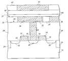
- FIG. 2illustrates a fragment of an integrated circuit incorporating a composition of the present invention. In referring to FIG. 2 , similar numbering to that utilized above in describing the prior art structure of FIG. 1 will be used, with differences indicated by different numerals.
- FIG. 2differs from the prior art structure of FIG. 1 in that FIG. 2 illustrates a barrier layer 100 in place of the silicon nitride barrier layer 38 of FIG. 1 .
- Layer 100can comprise, for example, an above-described novel composition of the present invention, such as, for example, (CH 3 ) x Si 3 N (4 ⁇ x) .
- layer 100can comprise a composition which includes carbon, silicon and nitrogen, and wherein the nitrogen is bonded to carbon.
- Layer 100is proximate conductive material 32 (actually against conductive material 32 ) and separates second conductive material 44 from first conductive material 32 . In the construction shown in FIG.
- barrier layer 100separates conductive material 32 from an insulative material 40 to impede migration of oxide from insulative material 40 into copper of a preferred conductive material 32 , as well as to impede migration of copper from preferred material 32 into insulative material 40 .
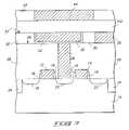
- FIG. 3illustrates an alternate embodiment semiconductor construction of the present invention (with numbering identical to that utilized in FIG. 2 ), wherein insulative material 40 ( FIG. 2 ) is eliminated.
- Barrier layer 100is thus the only material between first conductive material 32 and second conductive material 44 , and is against both conductive material 32 and conductive material 44 .
- barrier layer 100comprises (CH 3 ) x Si 3 N (4 ⁇ x) (wherein “x” is from about 1 to about 4, and preferably wherein “x” is about 0.7).
- Such barrier layer 100can be formed by the methods discussed above, and can, for example, consist essentially of Si 3 N y and (CH 3 ) x Si 3 N (4 ⁇ x) .
- an amount of (CH 3 ) x Si 3 N (4 ⁇ x) within barrier layer 100can be adjusted by the above-discussed methods of adjusting a ratio of SiH 4 and CH 3 SiH 3 during formation of the layer.
- An exemplary concentration of (CH 3 ) x Si 3 N (4 ⁇ x) within barrier layer 100is from greater than 0% to about 20% (mole percent).
Landscapes
- Engineering & Computer Science (AREA)
- Physics & Mathematics (AREA)
- Condensed Matter Physics & Semiconductors (AREA)
- General Physics & Mathematics (AREA)
- Computer Hardware Design (AREA)
- Microelectronics & Electronic Packaging (AREA)
- Power Engineering (AREA)
- Manufacturing & Machinery (AREA)
- Internal Circuitry In Semiconductor Integrated Circuit Devices (AREA)
Abstract
Description
This patent resulted from a continuation of U.S. patent application Ser. No. 09/641,826, filed on Aug. 17, 2000 now U.S. Pat. No. 6,719,919, which is a divisional application of U.S. patent application Ser. No. 09/219,041, which was filed on Dec. 23, 1998 now U.S. Pat. No. 6,828,683.
The invention pertains to compositions of matter comprising silicon bonded to both nitrogen and an organic material. The invention further pertains to semiconductor devices incorporating the above-described compositions of matter, and to methods of forming semiconductor devices. In particular aspects, the invention pertains to semiconductor devices incorporating copper-containing materials, and to methods of forming such devices.
It would be desirable to employ copper-containing materials in semiconductor devices. Copper has conductive properties that are superior to those of many of the conductive materials presently utilized in semiconductor devices. Unfortunately, copper has a drawback associated with it that it cannot generally be placed against oxide-comprising insulative materials (such as, for example, silicon dioxide). If copper-containing materials are placed adjacent oxide-comprising insulative materials, oxygen can diffuse into the copper-containing material and react to reduce conductivity of the material. Also, copper can diffuse into the oxide-containing material to reduce the insulative properties of the oxide-containing material. Additionally, copper can diffuse through oxide insulative material to device regions and cause degradation of device (e.g., transistor) performance. The problems associated with copper are occasionally addressed by providing nitride-containing barrier layers adjacent the copper-containing materials, but such can result in problems associated with parasitic capacitance, as illustrated inFIG. 1 . Specifically,FIG. 1 illustrates a fragment of a prior art integrated circuit, and illustrates regions where parasitic capacitance can occur.
The structure ofFIG. 1 comprises asubstrate 10, andtransistor gates overlying substrate 10.Substrate 10 can comprise, for example, monocrystalline silicon lightly doped with a p-type background conductivity-enhancing dopant. To aid in interpretation of the claims that follow, the term “semiconductive substrate” is defined to mean any construction comprising semiconductive material, including, but not limited to, bulk semiconductive materials such as a semiconductive wafer (either alone or in assemblies comprising other materials thereon), and semiconductive material layers (either alone or in assemblies comprising other materials). The term “substrate” refers to any supporting structure, including, but not limited to, the semiconductive substrates described above.
Aninsulative material 26 extends oversubstrate 10, and overtransistor gates conductive plug 28 extends throughinsulative material 26 to contactconductive diffusion region 20.Conductive plug 28 can comprise, for example, conductively doped polysilicon.Insulative material 26 can comprise, for example, silicon dioxide or borophosphosilicate glass (BPSG).Insulative material 26 andplug 28 together comprise a planarizedupper surface 29. Planarizedsurface 29 can be formed by, for example, chemical-mechanical polishing.
A secondinsulative material 30 is formed overinsulative material 26 and on planarizedupper surface 29. Secondinsulative material 30 can comprise, for example, borophosphosilicate glass or silicon dioxide. Aconductive material 32 is formed within an opening ininsulative material 30 and overconductive plug 28.Conductive material 32 comprises copper. The copper can be, for example, in the form of elemental copper, or in the form of an alloy.Conductive material 32 is separated fromconductive plug 28 by anintervening barrier layer 34.Barrier layer 34 typically comprises a conductive material, such as titanium nitride (TiN) or tantalum nitride (TaN), and is provided to prevent out-diffusion of copper fromconductive material 32 into eitherinsulative material 26 or the polysilicon ofconductive plug 28.Barrier layer 34 can also prevent diffusion of silicon or oxygen fromlayers conductive material 32. It is desired to prevent diffusion of oxygen to the copper ofmaterial 32, as such oxygen could otherwise reduce conductance ofmaterial 32. Also, it is desired to prevent copper diffusion frommaterial 32 intoinsulative layer 26, as such copper could reduce the insulative properties of the material oflayer 26. Additionally, diffusion throughlayer 26 and into one or more ofregions
A secondconductive material 36 is provided overinsulative material 26 and spaced from firstconductive material 32. Secondconductive material 36 can comprise, for example, conductively doped polysilicon or a conductive metal, or a combination of two or more conductive materials (such as copper and TiN). Secondconductive material 36 is spaced from firstconductive material 32 by an intervening region ofinsulative material 30 andbarrier layer 34.
Aninsulative barrier layer 38 is provided over planarizedupper surface 37.Insulative barrier layer 38 can comprise, for example, silicon nitride.
Aninsulative layer 40 is provided overinsulative barrier layer 38.Insulative layer 40 can comprise, for example, silicon dioxide or BPSG.Insulative barrier layer 38 inhibits diffusion of copper from firstconductive material 32 intoinsulative layer 40, and inhibits diffusion of oxygen frominsulative layer 40 into firstconductive material 32.
Anotherinsulative layer 42 is provided overinsulative layer 40, and a thirdconductive material 44 is provided withininsulative material 42 and over firstconductive material 32.Insulative material 42 can comprise, for example, BPSG or silicon dioxide, and thirdconductive material 44 can comprise, for example, conductively doped polysilicon or a metal, or a combination of two or more conductive materials (such as copper and TiN).
In one aspect, the invention encompasses a semiconductor processing method wherein a conductive copper-containing material is formed over a semiconductive substrate and a second material is formed proximate the conductive material. A barrier layer is formed between the conductive material and the second material. The barrier layer comprises a compound having silicon chemically bonded to both nitrogen and an organic material.
In another aspect, the invention encompasses a composition of matter comprising silicon chemically bonded to both nitrogen and an organic material.
In yet another aspect, the invention encompasses a semiconductor processing method. A semiconductive substrate is provided and a layer is formed over the semiconductive substrate. The layer comprises a compound having silicon chemically bonded to both nitrogen and an organic material.
Preferred embodiments of the invention are described below with reference to the following accompanying drawings.
This disclosure of the invention is submitted in furtherance of the constitutional purposes of the U.S. Patent Laws “to promote the progress of science and useful arts” (Article 1, Section 8).
In accordance with one aspect of the present invention, a novel composition of matter has been developed which comprises silicon chemically bonded to both nitrogen and an organic material, and wherein the nitrogen is not bonded to carbon. More specifically, the silicon is chemically bonded to both nitrogen and carbon. The carbon can be, for example, in the form of a hydrocarbon. In a preferred aspect, the carbon is comprised by a methyl group and the composition of matter consists essentially of (CH3)xSi3N(4−x), wherein x is greater than 0 and no greater than about 4.
A composition of the present invention can be formed by, for example, reacting inorganic silane with one or more of ammonia (NH3), hydrazine (N2H4), or a combination of nitrogen (N2) and hydrogen (H2). The reaction can occur with or without a plasma. However, if the reaction comprises an organic silane in combination with dinitrogen and dihydrogen, the reaction preferably occurs in the presence of plasma.
An exemplary reaction is to combine methylsilane (CH3SiH3) with ammonia (NH3) in the presence of a plasma to form (CH3)xSi3N4−x. The exemplary reaction can occur, for example, under the following conditions. A substrate is placed within a reaction chamber of a reactor, and a surface of the substrate is maintained at a temperature of from about 0° C. to about 600° C. Ammonia and methylsilane are flowed into the reaction chamber, and a pressure within the chamber is maintained at from about 300 mTorr to about 30 Torr, with a plasma at radio frequency (RF) power of from about 50 watts to about 500 watts. A product comprising (CH3)xSi3N(4−x)is then formed and deposited on the substrate. The reactor can comprise, for example, a cold wall plasma reactor.
It is found that the product deposited from the described reaction consists essentially of Si3Nyand (CH3)xSi3N(4−x), (wherein y is generally about 4/3, and x is also generally about 4/3). The (CH3)xSi3N(4−x)is present in the product to a concentration of from greater than 0% to about 50% (mole percent), and is preferably from about 10% to about 20%. The amount of (CH3)xSi3N(4−x)present in the product can be adjusted by providing a feed gas of SiH4in the reactor in addition to the CH3SiH3, and by varying a ratio of the SiH4to the CH3SiH3, and/or by adjusting RF power.
The compositions of matter encompassed by the present invention are found to be insulative, and to have lower dielectric constants than silicon nitride. Accordingly, compositions of the present invention can be substituted for silicon nitride in barrier layers to reduce parasitic capacitance between adjacent conductive components.FIG. 2 illustrates a fragment of an integrated circuit incorporating a composition of the present invention. In referring toFIG. 2 , similar numbering to that utilized above in describing the prior art structure ofFIG. 1 will be used, with differences indicated by different numerals.
The structure ofFIG. 2 differs from the prior art structure ofFIG. 1 in thatFIG. 2 illustrates abarrier layer 100 in place of the siliconnitride barrier layer 38 ofFIG. 1 .Layer 100 can comprise, for example, an above-described novel composition of the present invention, such as, for example, (CH3)xSi3N(4−x). Alternatively,layer 100 can comprise a composition which includes carbon, silicon and nitrogen, and wherein the nitrogen is bonded to carbon.Layer 100 is proximate conductive material32 (actually against conductive material32) and separates secondconductive material 44 from firstconductive material 32. In the construction shown inFIG. 2 ,barrier layer 100 separatesconductive material 32 from aninsulative material 40 to impede migration of oxide frominsulative material 40 into copper of a preferredconductive material 32, as well as to impede migration of copper from preferredmaterial 32 intoinsulative material 40.
In exemplary embodiments of the present invention,barrier layer 100 comprises (CH3)xSi3N(4−x)(wherein “x” is from about 1 to about 4, and preferably wherein “x” is about 0.7).Such barrier layer 100 can be formed by the methods discussed above, and can, for example, consist essentially of Si3Nyand (CH3)xSi3N(4−x). Also, an amount of (CH3)xSi3N(4−x)withinbarrier layer 100 can be adjusted by the above-discussed methods of adjusting a ratio of SiH4and CH3SiH3during formation of the layer. An exemplary concentration of (CH3)xSi3N(4−x)withinbarrier layer 100 is from greater than 0% to about 20% (mole percent).
In compliance with the statute, the invention has been described in language more or less specific as to structural and methodical features. It is to be understood, however, that the invention is not limited to the specific features shown and described, since the means herein disclosed comprise preferred forms of putting the invention into effect. The invention is, therefore, claimed in any of its forms or modifications within the proper scope of the appended claims appropriately interpreted in accordance with the doctrine of equivalents.
Claims (3)
1. A composition of matter consisting essentially of (CH3)xSi3N(4−x), with x being greater than 0 and no greater than 4, and Si3Nywhere y is about 4/3, the concentration of (CH3)xSi3N(4−x)being from greater than 0 mole % to about 20 mole %.
2. The composition ofclaim 1 wherein x is from about 1 to about 4.
3. The composition ofclaim 1 wherein x is about 0.7.
Priority Applications (1)
| Application Number | Priority Date | Filing Date | Title |
|---|---|---|---|
| US10/776,553US7279118B2 (en) | 1998-12-23 | 2004-02-10 | Compositions of matter and barrier layer compositions |
Applications Claiming Priority (3)
| Application Number | Priority Date | Filing Date | Title |
|---|---|---|---|
| US09/219,041US6828683B2 (en) | 1998-12-23 | 1998-12-23 | Semiconductor devices, and semiconductor processing methods |
| US09/641,826US6719919B1 (en) | 1998-12-23 | 2000-08-17 | Composition of matter |
| US10/776,553US7279118B2 (en) | 1998-12-23 | 2004-02-10 | Compositions of matter and barrier layer compositions |
Related Parent Applications (1)
| Application Number | Title | Priority Date | Filing Date |
|---|---|---|---|
| US09/641,826ContinuationUS6719919B1 (en) | 1998-12-23 | 2000-08-17 | Composition of matter |
Publications (2)
| Publication Number | Publication Date |
|---|---|
| US20040159875A1 US20040159875A1 (en) | 2004-08-19 |
| US7279118B2true US7279118B2 (en) | 2007-10-09 |
Family
ID=22817591
Family Applications (3)
| Application Number | Title | Priority Date | Filing Date |
|---|---|---|---|
| US09/219,041Expired - LifetimeUS6828683B2 (en) | 1998-12-23 | 1998-12-23 | Semiconductor devices, and semiconductor processing methods |
| US09/641,826Expired - LifetimeUS6719919B1 (en) | 1998-12-23 | 2000-08-17 | Composition of matter |
| US10/776,553Expired - Fee RelatedUS7279118B2 (en) | 1998-12-23 | 2004-02-10 | Compositions of matter and barrier layer compositions |
Family Applications Before (2)
| Application Number | Title | Priority Date | Filing Date |
|---|---|---|---|
| US09/219,041Expired - LifetimeUS6828683B2 (en) | 1998-12-23 | 1998-12-23 | Semiconductor devices, and semiconductor processing methods |
| US09/641,826Expired - LifetimeUS6719919B1 (en) | 1998-12-23 | 2000-08-17 | Composition of matter |
Country Status (1)
| Country | Link |
|---|---|
| US (3) | US6828683B2 (en) |
Cited By (2)
| Publication number | Priority date | Publication date | Assignee | Title |
|---|---|---|---|---|
| US20090191705A1 (en)* | 2008-01-24 | 2009-07-30 | Chung-Shi Liu | Semiconductor Contact Barrier |
| US9236253B2 (en) | 2012-08-17 | 2016-01-12 | Taiwan Semiconductor Manufacturing Company, Ltd. | Strained structure of a semiconductor device |
Families Citing this family (6)
| Publication number | Priority date | Publication date | Assignee | Title |
|---|---|---|---|---|
| US7067861B1 (en)* | 1998-11-25 | 2006-06-27 | Micron Technology, Inc. | Device and method for protecting against oxidation of a conductive layer in said device |
| US6828683B2 (en)* | 1998-12-23 | 2004-12-07 | Micron Technology, Inc. | Semiconductor devices, and semiconductor processing methods |
| JP4363716B2 (en)* | 1999-06-25 | 2009-11-11 | 株式会社東芝 | LSI wiring structure design method |
| US7067414B1 (en) | 1999-09-01 | 2006-06-27 | Micron Technology, Inc. | Low k interlevel dielectric layer fabrication methods |
| US6784485B1 (en)* | 2000-02-11 | 2004-08-31 | International Business Machines Corporation | Diffusion barrier layer and semiconductor device containing same |
| JP3716218B2 (en) | 2002-03-06 | 2005-11-16 | 富士通株式会社 | Wiring structure and method for forming the same |
Citations (222)
| Publication number | Priority date | Publication date | Assignee | Title |
|---|---|---|---|---|
| GB593727A (en) | 1944-07-01 | 1947-10-23 | British Thomson Houston Co Ltd | Improvements in and relating to methods of rendering materials water-repellent |
| US4158717A (en) | 1977-02-14 | 1979-06-19 | Varian Associates, Inc. | Silicon nitride film and method of deposition |
| US4444617A (en) | 1983-01-06 | 1984-04-24 | Rockwell International Corporation | Reactive ion etching of molybdenum silicide and N+ polysilicon |
| US4474975A (en) | 1983-05-09 | 1984-10-02 | The United States Of America As Represented By The Administrator Of The National Aeronautics And Space Administration | Process for producing tris (N-methylamino) methylsilane |
| US4523214A (en) | 1981-07-03 | 1985-06-11 | Fuji Photo Film Co., Ltd. | Solid state image pickup device utilizing microcrystalline and amorphous silicon |
| US4552783A (en) | 1984-11-05 | 1985-11-12 | General Electric Company | Enhancing the selectivity of tungsten deposition on conductor and semiconductor surfaces |
| US4562091A (en) | 1982-12-23 | 1985-12-31 | International Business Machines Corporation | Use of plasma polymerized orgaosilicon films in fabrication of lift-off masks |
| US4592129A (en) | 1985-04-01 | 1986-06-03 | Motorola, Inc. | Method of making an integral, multiple layer antireflection coating by hydrogen ion implantation |
| US4600671A (en) | 1983-09-12 | 1986-07-15 | Canon Kabushiki Kaisha | Photoconductive member having light receiving layer of A-(Si-Ge) and N |
| US4648904A (en) | 1986-02-14 | 1987-03-10 | Scm Corporation | Aqueous systems containing silanes for rendering masonry surfaces water repellant |
| US4695859A (en) | 1986-10-20 | 1987-09-22 | Energy Conversion Devices, Inc. | Thin film light emitting diode, photonic circuit employing said diode imager employing said circuits |
| US4702936A (en) | 1984-09-20 | 1987-10-27 | Applied Materials Japan, Inc. | Gas-phase growth process |
| US4755478A (en) | 1987-08-13 | 1988-07-05 | International Business Machines Corporation | Method of forming metal-strapped polysilicon gate electrode for FET device |
| US4764247A (en) | 1987-03-18 | 1988-08-16 | Syn Labs, Inc. | Silicon containing resists |
| JPS63157443U (en) | 1987-03-30 | 1988-10-14 | ||
| JPS63316476A (en) | 1987-06-18 | 1988-12-23 | Seiko Instr & Electronics Ltd | Semiconductor device and manufacture thereof |
| US4805683A (en) | 1988-03-04 | 1989-02-21 | International Business Machines Corporation | Method for producing a plurality of layers of metallurgy |
| US4833096A (en) | 1988-01-19 | 1989-05-23 | Atmel Corporation | EEPROM fabrication process |
| US4863755A (en) | 1987-10-16 | 1989-09-05 | The Regents Of The University Of California | Plasma enhanced chemical vapor deposition of thin films of silicon nitride from cyclic organosilicon nitrogen precursors |
| US4870470A (en) | 1987-10-16 | 1989-09-26 | International Business Machines Corporation | Non-volatile memory cell having Si rich silicon nitride charge trapping layer |
| US4910160A (en) | 1989-06-06 | 1990-03-20 | National Semiconductor Corporation | High voltage complementary NPN/PNP process |
| US4940509A (en) | 1988-03-25 | 1990-07-10 | Texas Instruments, Incorporated | Isotropic etchant for capped silicide processes |
| US4971655A (en) | 1989-12-26 | 1990-11-20 | Micron Technology, Inc. | Protection of a refractory metal silicide during high-temperature processing using a dual-layer cap of silicon dioxide and silicon nitride |
| US4992306A (en) | 1990-02-01 | 1991-02-12 | Air Products Abd Chemicals, Inc. | Deposition of silicon dioxide and silicon oxynitride films using azidosilane sources |
| US5034348A (en) | 1990-08-16 | 1991-07-23 | International Business Machines Corp. | Process for forming refractory metal silicide layers of different thicknesses in an integrated circuit |
| US5036383A (en) | 1989-04-27 | 1991-07-30 | Kabushiki Kaisha Toshiba | Semiconductor device having an improved bonding pad |
| US5061509A (en) | 1989-08-25 | 1991-10-29 | Kabushiki Kaisha Toshiba | Method of manufacturing polyimide thin film and method of manufacturing liquid crystal orientation film of polyimide |
| EP0464515A3 (en) | 1990-06-28 | 1992-05-06 | Kabushiki Kaisha Toshiba | Method of manufacturing silicon nitride film |
| US5140390A (en) | 1990-02-16 | 1992-08-18 | Hughes Aircraft Company | High speed silicon-on-insulator device |
| US5219613A (en) | 1990-06-13 | 1993-06-15 | Wacker-Chemitronic Gesellschaft Fur Elektronik-Grundstoffe Mbh | Process for producing storage-stable surfaces of polished silicon wafers |
| US5244537A (en) | 1989-12-27 | 1993-09-14 | Honeywell, Inc. | Fabrication of an electronic microvalve apparatus |
| JPH05263255A (en) | 1992-03-19 | 1993-10-12 | Hitachi Electron Eng Co Ltd | Plasma cvd device |
| US5260600A (en) | 1990-06-05 | 1993-11-09 | Mitsubishi Denki Kabushiki Kaisha | Semiconductor device having protective insulating film |
| US5270267A (en) | 1989-05-31 | 1993-12-14 | Mitel Corporation | Curing and passivation of spin on glasses by a plasma process wherein an external polarization field is applied to the substrate |
| US5276347A (en) | 1991-12-18 | 1994-01-04 | Sgs-Thomson Microelectronics, Inc. | Gate overlapping LDD structure |
| US5285017A (en) | 1991-12-31 | 1994-02-08 | Intel Corporation | Embedded ground plane and shielding structures using sidewall insulators in high frequency circuits having vias |
| US5286661A (en) | 1992-08-26 | 1994-02-15 | Motorola, Inc. | Method of forming a bipolar transistor having an emitter overhang |
| JPH0667019A (en) | 1992-01-17 | 1994-03-11 | Asahi Glass Co Ltd | Antireflection layer and its production |
| EP0588087A2 (en) | 1992-08-20 | 1994-03-23 | Sony Corporation | Method of determining optimum optical conditions for an anti-reflective layer used in a method of forming a resist pattern |
| US5302366A (en) | 1991-03-28 | 1994-04-12 | Phillips Petroleum Company | Production of silicon product containing both carbon and nitrogen |
| US5312768A (en) | 1993-03-09 | 1994-05-17 | Micron Technology, Inc. | Integrated process for fabricating raised, source/drain, short-channel transistors |
| US5314724A (en) | 1991-01-08 | 1994-05-24 | Fujitsu Limited | Process for forming silicon oxide film |
| US5340621A (en) | 1992-03-30 | 1994-08-23 | Nippon Sheet Glass Co., Ltd. | Plasma CVD method |
| JPH06244172A (en) | 1993-02-18 | 1994-09-02 | Toray Ind Inc | Multilayered wiring structure |
| US5356515A (en) | 1990-10-19 | 1994-10-18 | Tokyo Electron Limited | Dry etching method |
| US5376591A (en) | 1992-06-05 | 1994-12-27 | Semiconductor Process Laboratory Co., Ltd. | Method for manufacturing semiconductor device |
| US5405489A (en) | 1991-10-30 | 1995-04-11 | Samsung Electronics Co., Ltd. | Method for fabricating an interlayer-dielectric film of a semiconductor device by using a plasma treatment prior to reflow |
| US5413963A (en) | 1994-08-12 | 1995-05-09 | United Microelectronics Corporation | Method for depositing an insulating interlayer in a semiconductor metallurgy system |
| US5429987A (en) | 1993-01-25 | 1995-07-04 | Sharp Microelectronics Technology, Inc. | Method for profile control of selective metallization |
| US5439838A (en) | 1994-09-14 | 1995-08-08 | United Microelectronics Corporation | Method of thinning for EEPROM tunneling oxide device |
| US5441797A (en) | 1993-04-27 | 1995-08-15 | International Business Machines Corporation | Antireflective polyimide dielectric for photolithography |
| US5461003A (en) | 1994-05-27 | 1995-10-24 | Texas Instruments Incorporated | Multilevel interconnect structure with air gaps formed between metal leads |
| US5470772A (en) | 1991-11-06 | 1995-11-28 | Intel Corporation | Silicidation method for contactless EPROM related devices |
| US5472827A (en) | 1991-12-30 | 1995-12-05 | Sony Corporation | Method of forming a resist pattern using an anti-reflective layer |
| US5472829A (en) | 1991-12-30 | 1995-12-05 | Sony Corporation | Method of forming a resist pattern by using an anti-reflective layer |
| US5482894A (en) | 1994-08-23 | 1996-01-09 | Texas Instruments Incorporated | Method of fabricating a self-aligned contact using organic dielectric materials |
| JPH0845926A (en) | 1994-07-26 | 1996-02-16 | Sony Corp | Semiconductor device and its manufacture |
| US5498555A (en) | 1994-11-07 | 1996-03-12 | United Microelectronics Corporation | Method of making LDD with polysilicon and dielectric spacers |
| US5536857A (en) | 1994-07-05 | 1996-07-16 | Ford Motor Company | Single source volatile precursor for SiO2.TiO2 powders and films |
| US5541445A (en) | 1991-08-14 | 1996-07-30 | Mitel Corporation | High performance passivation for semiconductor devices |
| US5543654A (en) | 1992-01-28 | 1996-08-06 | Thunderbird Technologies, Inc. | Contoured-tub fermi-threshold field effect transistor and method of forming same |
| JPH08213386A (en) | 1995-02-08 | 1996-08-20 | Fujitsu Ltd | Method for manufacturing semiconductor device |
| US5554567A (en) | 1994-09-01 | 1996-09-10 | Taiwan Semiconductor Manufacturing Company Ltd. | Method for improving adhesion to a spin-on-glass |
| US5591494A (en) | 1993-09-24 | 1997-01-07 | Applied Materials, Inc. | Deposition of silicon nitrides by plasma-enhanced chemical vapor deposition |
| US5593741A (en) | 1992-11-30 | 1997-01-14 | Nec Corporation | Method and apparatus for forming silicon oxide film by chemical vapor deposition |
| US5600165A (en) | 1994-07-27 | 1997-02-04 | Sony Corporation | Semiconductor device with antireflection film |
| JPH0950993A (en) | 1995-08-08 | 1997-02-18 | Fujitsu Ltd | Insulating film forming method and semiconductor device |
| JPH0955351A (en) | 1995-08-15 | 1997-02-25 | Sony Corp | Manufacture of semiconductor device |
| EP0771886A1 (en) | 1995-10-30 | 1997-05-07 | Dow Corning Corporation | Method for depositing amorphous SiNC coatings |
| EP0778496A2 (en) | 1995-12-05 | 1997-06-11 | Applied Materials, Inc. | Method and apparatus for depositing antireflective coating |
| US5639687A (en) | 1993-07-06 | 1997-06-17 | Motorola Inc. | Method for forming an integrated circuit pattern on a semiconductor substrate using silicon-rich silicon nitride |
| US5652187A (en) | 1991-10-30 | 1997-07-29 | Samsung Electronics Co., Ltd. | Method for fabricating doped interlayer-dielectric film of semiconductor device using a plasma treatment |
| US5656330A (en) | 1994-03-22 | 1997-08-12 | Futaba Denshi Kogyo K.K. | Resistive element having a resistivity which is thermally stable against heat treatment, and method and apparatus for producing same |
| US5656337A (en) | 1993-08-31 | 1997-08-12 | Samsung Electronics Co., Ltd. | Method of forming a dielectric layer |
| US5661093A (en) | 1996-09-12 | 1997-08-26 | Applied Materials, Inc. | Method for the stabilization of halogen-doped films through the use of multiple sealing layers |
| US5667015A (en) | 1995-02-03 | 1997-09-16 | Bj Services Company | Well barrier |
| US5670297A (en) | 1991-12-30 | 1997-09-23 | Sony Corporation | Process for the formation of a metal pattern |
| US5674356A (en) | 1994-04-05 | 1997-10-07 | Sony Corporation | Method for forming a semiconductor device in which an anti reflective layer is formed by varying the composition thereof |
| US5677015A (en) | 1994-03-17 | 1997-10-14 | Sony Corporation | High dielectric constant material containing tantalum, process for forming high dielectric constant film containing tantalum, and semiconductor device using the same |
| US5677111A (en) | 1991-12-20 | 1997-10-14 | Sony Corporation | Process for production of micropattern utilizing antireflection film |
| US5691212A (en) | 1996-09-27 | 1997-11-25 | Taiwan Semiconductor Manufacturing Company, Ltd. | MOS device structure and integration method |
| US5709741A (en) | 1995-02-28 | 1998-01-20 | Dow Corning Toray Silicone Co., Ltd. | Water repellent for application to glass and water-repellent glass |
| US5710067A (en) | 1995-06-07 | 1998-01-20 | Advanced Micro Devices, Inc. | Silicon oxime film |
| US5711987A (en)* | 1996-10-04 | 1998-01-27 | Dow Corning Corporation | Electronic coatings |
| US5731242A (en) | 1993-10-15 | 1998-03-24 | Intel Corporation | Self-aligned contact process in semiconductor fabrication |
| US5741721A (en) | 1994-02-01 | 1998-04-21 | Quality Microcircuits Corporation | Method of forming capacitors and interconnect lines |
| US5744399A (en) | 1995-11-13 | 1998-04-28 | Lsi Logic Corporation | Process for forming low dielectric constant layers using fullerenes |
| US5747388A (en) | 1992-09-18 | 1998-05-05 | Siemens Aktiengesellschaft | Antireflection layer and process for lithographically structuring a layer |
| US5750442A (en) | 1995-09-25 | 1998-05-12 | Micron Technology, Inc. | Germanium as an antireflective coating and method of use |
| US5753320A (en) | 1985-09-26 | 1998-05-19 | Canon Kabushiki Kaisha | Process for forming deposited film |
| US5759755A (en) | 1993-08-08 | 1998-06-02 | Samsung Electronics, Co., Ltd. | Semiconductor substrate containing anti-reflective layer |
| US5759746A (en) | 1996-05-24 | 1998-06-02 | Kabushiki Kaisha Toshiba | Fabrication process using a thin resist |
| JPH10163083A (en) | 1996-10-15 | 1998-06-19 | Texas Instr Inc <Ti> | Semiconductor treatment method |
| US5783493A (en) | 1997-01-27 | 1998-07-21 | Taiwan Semiconductor Manufacturing Company Ltd. | Method for reducing precipitate defects using a plasma treatment post BPSG etchback |
| US5786039A (en) | 1995-05-15 | 1998-07-28 | France Telecom | Process for electrical insulation in microelectronics, applicable in narrow cavities, by deposition of oxide in the viscous state and corresponding device |
| US5789819A (en) | 1994-05-20 | 1998-08-04 | Texas Instruments Incorporated | Low dielectric constant material for electronics applications |
| US5792689A (en) | 1997-04-11 | 1998-08-11 | Vanguard International Semiconducter Corporation | Method for manufacturing double-crown capacitors self-aligned to node contacts on dynamic random access memory |
| US5796151A (en) | 1996-12-19 | 1998-08-18 | Texas Instruments Incorporated | Semiconductor stack having a dielectric sidewall for prevention of oxidation of tungsten in tungsten capped poly-silicon gate electrodes |
| US5800877A (en) | 1995-08-18 | 1998-09-01 | Canon Sales Co., Inc. | Method for forming a fluorine containing silicon oxide film |
| US5801399A (en) | 1994-10-13 | 1998-09-01 | Yamaha Corporation | Semiconductor device with antireflection film |
| US5807660A (en) | 1997-02-03 | 1998-09-15 | Taiwan Semiconductor Manufacturing Company Ltd. | Avoid photoresist lifting by post-oxide-dep plasma treatment |
| US5817549A (en) | 1994-08-31 | 1998-10-06 | Semiconductor Energy Laboratory Co., Ltd. | Method for manufacturing a semiconductor device |
| US5838052A (en) | 1996-03-07 | 1998-11-17 | Micron Technology, Inc. | Reducing reflectivity on a semiconductor wafer by annealing titanium and aluminum |
| US5840610A (en) | 1997-01-16 | 1998-11-24 | Advanced Micro Devices, Inc. | Enhanced oxynitride gate dielectrics using NF3 gas |
| US5858880A (en) | 1994-05-14 | 1999-01-12 | Trikon Equipment Limited | Method of treating a semi-conductor wafer |
| US5872035A (en) | 1996-06-29 | 1999-02-16 | Hyundai Electronics Industries Co., Ltd. | Method of forming a floating gate in a flash memory device |
| US5872385A (en) | 1994-05-02 | 1999-02-16 | Motorola Inc. | Conductive interconnect structure and method of formation |
| US5874367A (en) | 1992-07-04 | 1999-02-23 | Trikon Technologies Limited | Method of treating a semi-conductor wafer |
| US5883014A (en) | 1997-06-03 | 1999-03-16 | United Microelectronics Corp. | Method for treating via sidewalls with hydrogen plasma |
| US5883011A (en) | 1997-06-18 | 1999-03-16 | Vlsi Technology, Inc. | Method of removing an inorganic antireflective coating from a semiconductor substrate |
| US5933721A (en) | 1997-04-21 | 1999-08-03 | Advanced Micro Devices, Inc. | Method for fabricating differential threshold voltage transistor pair |
| US5948482A (en) | 1995-09-19 | 1999-09-07 | University Of New Mexico | Ambient pressure process for preparing aerogel thin films reliquified sols useful in preparing aerogel thin films |
| EP0942330A1 (en) | 1998-03-11 | 1999-09-15 | Applied Materials, Inc. | Process for depositing and developing a plasma polymerized organosilicon photoresist film |
| US5960289A (en) | 1998-06-22 | 1999-09-28 | Motorola, Inc. | Method for making a dual-thickness gate oxide layer using a nitride/oxide composite region |
| US5962581A (en) | 1995-04-28 | 1999-10-05 | Kabushiki Kaisha Toshiba | Silicone polymer composition, method of forming a pattern and method of forming an insulating film |
| US5968611A (en) | 1997-11-26 | 1999-10-19 | The Research Foundation Of State University Of New York | Silicon nitrogen-based films and method of making the same |
| US5981368A (en) | 1998-11-05 | 1999-11-09 | Advanced Micro Devices | Enhanced shallow junction design by polysilicon line width reduction using oxidation with integrated spacer formation |
| US5985519A (en) | 1997-03-19 | 1999-11-16 | Fujitsu Limited | Method of manufacturing semiconductor device using top antireflection film |
| US5986318A (en) | 1996-10-24 | 1999-11-16 | Samsung Electronics Co., Ltd. | (Ge,Si) Nx anti-reflective compositions and integrated circuit devices comprising the same |
| US5991217A (en) | 1996-12-26 | 1999-11-23 | Micro Magic, Inc. | Fast SRAM design using embedded sense amps |
| US5994730A (en) | 1996-11-21 | 1999-11-30 | Alliance Semiconductor Corporation | DRAM cell having storage capacitor contact self-aligned to bit lines and word lines |
| US5994217A (en) | 1996-12-16 | 1999-11-30 | Chartered Semiconductor Manufacturing Ltd. | Post metallization stress relief annealing heat treatment for ARC TiN over aluminum layers |
| US6001747A (en) | 1998-07-22 | 1999-12-14 | Vlsi Technology, Inc. | Process to improve adhesion of cap layers in integrated circuits |
| US6001741A (en) | 1998-04-15 | 1999-12-14 | Lucent Technologies Inc. | Method for making field effect devices and capacitors with improved thin film dielectrics and resulting devices |
| US6004850A (en) | 1998-02-23 | 1999-12-21 | Motorola Inc. | Tantalum oxide anti-reflective coating (ARC) integrated with a metallic transistor gate electrode and method of formation |
| US6008121A (en) | 1996-03-19 | 1999-12-28 | Siemens Aktiengesellschaft | Etching high aspect contact holes in solid state devices |
| US6008124A (en) | 1996-02-22 | 1999-12-28 | Matsushita Electric Industrial Co., Ltd. | Semiconductor device having improved lamination-structure reliability for buried layers, silicide films and metal films, and a method for forming the same |
| US6017614A (en) | 1997-07-14 | 2000-01-25 | Vanguard International Semiconductor Corporation | Plasma-enhanced chemical vapor deposited SIO2 /SI3 N4 multilayer passivation layer for semiconductor applications |
| US6020243A (en) | 1997-07-24 | 2000-02-01 | Texas Instruments Incorporated | Zirconium and/or hafnium silicon-oxynitride gate dielectric |
| US6022404A (en) | 1995-01-12 | 2000-02-08 | Degussa Aktiengesellschaft | Surface-modified, pyrogenically produced mixed oxides, method of their production and use |
| US6028015A (en) | 1999-03-29 | 2000-02-22 | Lsi Logic Corporation | Process for treating damaged surfaces of low dielectric constant organo silicon oxide insulation material to inhibit moisture absorption |
| US6030901A (en) | 1999-06-24 | 2000-02-29 | Advanced Micro Devices, Inc. | Photoresist stripping without degrading low dielectric constant materials |
| JP2000068261A (en) | 1998-08-19 | 2000-03-03 | Toshiba Corp | Method for manufacturing semiconductor device |
| US6037228A (en) | 1999-02-12 | 2000-03-14 | United Microelectronics Corp. | Method of fabricating self-aligned contact window which includes forming a undoped polysilicon spacer that extends into a recess of the gate structure |
| US6040619A (en) | 1995-06-07 | 2000-03-21 | Advanced Micro Devices | Semiconductor device including antireflective etch stop layer |
| US6054379A (en) | 1998-02-11 | 2000-04-25 | Applied Materials, Inc. | Method of depositing a low k dielectric with organo silane |
| US6057217A (en) | 1996-07-25 | 2000-05-02 | Nec Corporation | Process for production of semiconductor device with foreign element introduced into silicon dioxide film |
| US6060766A (en) | 1997-08-25 | 2000-05-09 | Advanced Micro Devices, Inc. | Protection of hydrogen sensitive regions in semiconductor devices from the positive charge associated with plasma deposited barriers or layers |
| US6060765A (en) | 1998-01-05 | 2000-05-09 | Mitsubishi Denki Kabushiki Kaisha | Semiconductor device and a method of manufacturing the same |
| US6071799A (en) | 1997-06-30 | 2000-06-06 | Hyundai Electronics Industries Co., Ltd. | Method of forming a contact of a semiconductor device |
| US6080529A (en) | 1997-12-12 | 2000-06-27 | Applied Materials, Inc. | Method of etching patterned layers useful as masking during subsequent etching or for damascene structures |
| US6083852A (en) | 1997-05-07 | 2000-07-04 | Applied Materials, Inc. | Method for applying films using reduced deposition rates |
| US6087267A (en) | 1986-03-04 | 2000-07-11 | Motorola, Inc. | Process for forming an integrated circuit |
| US6087064A (en) | 1998-09-03 | 2000-07-11 | International Business Machines Corporation | Silsesquioxane polymers, method of synthesis, photoresist composition, and multilayer lithographic method |
| US6096656A (en) | 1999-06-24 | 2000-08-01 | Sandia Corporation | Formation of microchannels from low-temperature plasma-deposited silicon oxynitride |
| US6114736A (en) | 1996-10-29 | 2000-09-05 | International Business Machines Corporation | Controlled dopant diffusion and metal contamination in thin polycide gate conductor of MOSFET device |
| US6118163A (en) | 1998-02-04 | 2000-09-12 | Advanced Micro Devices, Inc. | Transistor with integrated poly/metal gate electrode |
| US6121133A (en) | 1997-08-22 | 2000-09-19 | Micron Technology, Inc. | Isolation using an antireflective coating |
| US6124641A (en) | 1997-06-26 | 2000-09-26 | Mitsubishi Denki Kabushiki Kaisha | Semiconductor device organic insulator film |
| US6130168A (en) | 1999-07-08 | 2000-10-10 | Taiwan Semiconductor Manufacturing Company | Using ONO as hard mask to reduce STI oxide loss on low voltage device in flash or EPROM process |
| US6133096A (en) | 1998-12-10 | 2000-10-17 | Su; Hung-Der | Process for simultaneously fabricating a stack gate flash memory cell and salicided periphereral devices |
| US6133613A (en) | 1998-02-03 | 2000-10-17 | Vanguard International Semiconductor Corporation | Anti-reflection oxynitride film for tungsten-silicide substrates |
| US6133618A (en) | 1997-08-14 | 2000-10-17 | Lucent Technologies Inc. | Semiconductor device having an anti-reflective layer and a method of manufacture thereof |
| US6136636A (en) | 1998-03-25 | 2000-10-24 | Texas Instruments - Acer Incorporated | Method of manufacturing deep sub-micron CMOS transistors |
| US6140151A (en) | 1998-05-22 | 2000-10-31 | Micron Technology, Inc. | Semiconductor wafer processing method |
| US6140677A (en) | 1998-06-26 | 2000-10-31 | Advanced Micro Devices, Inc. | Semiconductor topography for a high speed MOSFET having an ultra narrow gate |
| US6143670A (en) | 1998-12-28 | 2000-11-07 | Taiwan Semiconductor Manufacturing Company | Method to improve adhesion between low dielectric constant layer and silicon containing dielectric layer |
| US6153504A (en) | 1999-08-16 | 2000-11-28 | Advanced Micro Devices, Inc. | Method of using a silicon oxynitride ARC for final metal layer |
| US6156674A (en) | 1998-11-25 | 2000-12-05 | Micron Technology, Inc. | Semiconductor processing methods of forming insulative materials |
| US6156485A (en) | 1999-01-19 | 2000-12-05 | Taiwan Semiconductor Manufacturing Company Ltd. | Film scheme to solve high aspect ratio metal etch masking layer selectivity and improve photo I-line PR resolution capability in quarter-micron technology |
| US6159871A (en) | 1998-05-29 | 2000-12-12 | Dow Corning Corporation | Method for producing hydrogenated silicon oxycarbide films having low dielectric constant |
| US6159804A (en) | 1998-09-02 | 2000-12-12 | Advanced Micro Devices, Inc. | Disposable sidewall oxidation fabrication method for making a transistor having an ultra short channel length |
| US6184158B1 (en) | 1996-12-23 | 2001-02-06 | Lam Research Corporation | Inductively coupled plasma CVD |
| US6184151B1 (en) | 1997-08-21 | 2001-02-06 | International Business Machines Corporation | Method for forming cornered images on a substrate and photomask formed thereby |
| US6187694B1 (en) | 1997-11-10 | 2001-02-13 | Intel Corporation | Method of fabricating a feature in an integrated circuit using two edge definition layers and a spacer |
| US6187657B1 (en) | 1999-03-24 | 2001-02-13 | Advanced Micro Devices, Inc. | Dual material gate MOSFET technique |
| US6198144B1 (en) | 1999-08-18 | 2001-03-06 | Micron Technology, Inc. | Passivation of sidewalls of a word line stack |
| US6200863B1 (en) | 1999-03-24 | 2001-03-13 | Advanced Micro Devices, Inc. | Process for fabricating a semiconductor device having assymetric source-drain extension regions |
| US6200835B1 (en) | 1994-10-07 | 2001-03-13 | Micron Technology, Inc. | Methods of forming conductive polysilicon lines and bottom gated thin film transistors, and conductive polysilicon lines and thin film transistors |
| US6204168B1 (en) | 1998-02-02 | 2001-03-20 | Applied Materials, Inc. | Damascene structure fabricated using a layer of silicon-based photoresist material |
| US6208004B1 (en) | 1998-08-19 | 2001-03-27 | Philips Semiconductor, Inc. | Semiconductor device with high-temperature-stable gate electrode for sub-micron applications and fabrication thereof |
| US6209484B1 (en) | 1996-06-28 | 2001-04-03 | Applied Materials, Inc. | Method and apparatus for depositing an etch stop layer |
| US6218292B1 (en) | 1997-12-18 | 2001-04-17 | Advanced Micro Devices, Inc. | Dual layer bottom anti-reflective coating |
| US6225217B1 (en) | 1997-06-27 | 2001-05-01 | Nec Corporation | Method of manufacturing semiconductor device having multilayer wiring |
| US6235568B1 (en) | 1999-01-22 | 2001-05-22 | Intel Corporation | Semiconductor device having deposited silicon regions and a method of fabrication |
| US6235591B1 (en) | 1999-10-25 | 2001-05-22 | Chartered Semiconductor Manufacturing Company | Method to form gate oxides of different thicknesses on a silicon substrate |
| US6238976B1 (en) | 1997-07-08 | 2001-05-29 | Micron Technology, Inc. | Method for forming high density flash memory |
| US20010003064A1 (en) | 1999-12-02 | 2001-06-07 | Nec Corporation | Method for fabricating semiconductor device and apparatus for fabricating same |
| US6268282B1 (en) | 1998-09-03 | 2001-07-31 | Micron Technology, Inc. | Semiconductor processing methods of forming and utilizing antireflective material layers, and methods of forming transistor gate stacks |
| US6274292B1 (en) | 1998-02-25 | 2001-08-14 | Micron Technology, Inc. | Semiconductor processing methods |
| US6281100B1 (en) | 1998-09-03 | 2001-08-28 | Micron Technology, Inc. | Semiconductor processing methods |
| US6284677B1 (en) | 1997-04-18 | 2001-09-04 | United Semiconductor Corp. | Method of forming fluorosilicate glass (FSG) layers with moisture-resistant capability |
| US20010019868A1 (en) | 1999-07-23 | 2001-09-06 | Fernando Gonzalez | Field effect transistor assemblies, integrated circuitry, and methods of forming field effect transistors and integrated circuitry |
| US20010038919A1 (en) | 2000-03-20 | 2001-11-08 | Berry Ivan L. | Plasma curing process for porous silica thin film |
| US6323101B1 (en) | 1998-09-03 | 2001-11-27 | Micron Technology, Inc. | Semiconductor processing methods, methods of forming silicon dioxide methods of forming trench isolation regions, and methods of forming interlevel dielectric layers |
| EP1172845A2 (en) | 2000-07-14 | 2002-01-16 | Applied Materials, Inc. | Method for treating dielectric layers with low dielectric constant to reduce oxygen diffusion |
| US6348407B1 (en) | 2001-03-15 | 2002-02-19 | Chartered Semiconductor Manufacturing Inc. | Method to improve adhesion of organic dielectrics in dual damascene interconnects |
| US20020020919A1 (en)* | 1998-12-23 | 2002-02-21 | Weimin Li | Semiconductor devices, and semiconductor processing methods |
| US20020033486A1 (en) | 2000-08-04 | 2002-03-21 | Samsung Electronics Co., Ltd. | Method for forming an interconnection line using a hydrosilsesquioxane (HSQ) layer as an interlayer insulating layer |
| US6373114B1 (en) | 1998-10-23 | 2002-04-16 | Micron Technology, Inc. | Barrier in gate stack for improved gate dielectric integrity |
| US6383951B1 (en) | 1998-09-03 | 2002-05-07 | Micron Technology, Inc. | Low dielectric constant material for integrated circuit fabrication |
| US6403464B1 (en) | 1999-11-03 | 2002-06-11 | Taiwan Semiconductor Manufacturing Company | Method to reduce the moisture content in an organic low dielectric constant material |
| US20020081834A1 (en) | 2000-12-26 | 2002-06-27 | Honeywell International Inc. | Method for eliminating reaction between photoresist and OSG |
| US6429115B1 (en) | 2001-02-27 | 2002-08-06 | United Microelectronics Corp. | Method of manufacturing multilevel interconnects including performing a surface treatment to form a hydrophilic surface layer |
| US6432791B1 (en) | 1999-04-14 | 2002-08-13 | Texas Instruments Incorporated | Integrated circuit capacitor and method |
| US6435943B1 (en) | 2000-10-26 | 2002-08-20 | United Microelectronics Corp. | Method of chemical mechanical polishing organic silicon material with low dielectric constant |
| US6436808B1 (en) | 2000-12-07 | 2002-08-20 | Advanced Micro Devices, Inc. | NH3/N2-plasma treatment to prevent organic ILD degradation |
| US6440860B1 (en) | 2000-01-18 | 2002-08-27 | Micron Technology, Inc. | Semiconductor processing methods of transferring patterns from patterned photoresists to materials, and structures comprising silicon nitride |
| US6444593B1 (en) | 1998-12-02 | 2002-09-03 | Advanced Micro Devices, Inc. | Surface treatment of low-K SiOF to prevent metal interaction |
| US6451504B2 (en) | 1995-12-04 | 2002-09-17 | Micron Technology, Inc. | Semiconductor processing method of promoting photoresist adhesion to an outer substrate layer predominately comprising silicon nitride |
| US6465372B1 (en) | 1999-08-17 | 2002-10-15 | Applied Materials, Inc. | Surface treatment of C-doped SiO2 film to enhance film stability during O2 ashing |
| US6486057B1 (en) | 2001-04-12 | 2002-11-26 | National Science Council | Process for preparing Cu damascene interconnection |
| US6486061B1 (en) | 1999-08-17 | 2002-11-26 | Applied Materials, Inc. | Post-deposition treatment to enhance properties of Si-O-C low K films |
| US6492688B1 (en) | 1999-03-02 | 2002-12-10 | Siemens Aktiengesellschaft | Dual work function CMOS device |
| US6498084B2 (en) | 2001-05-14 | 2002-12-24 | Maxim Integrated Products, Inc. | Method of forming high density EEPROM cell |
| US6503818B1 (en) | 1999-04-02 | 2003-01-07 | Taiwan Semiconductor Manufacturing Company | Delamination resistant multi-layer composite dielectric layer employing low dielectric constant dielectric material |
| US20030013311A1 (en) | 2001-07-03 | 2003-01-16 | Ting-Chang Chang | Method of avoiding dielectric layer deterioation with a low dielectric constant during a stripping process |
| US6518122B1 (en) | 1999-12-17 | 2003-02-11 | Chartered Semiconductor Manufacturing Ltd. | Low voltage programmable and erasable flash EEPROM |
| US20030077916A1 (en) | 2001-10-11 | 2003-04-24 | Applied Materials, Inc. | Method of eliminating photoresist poisoning in damascene applications |
| US20030164354A1 (en) | 1999-12-28 | 2003-09-04 | Applied Materials, Inc. | System level in-situ integrated dielectric etch process particularly useful for copper dual damascene |
| US20030173671A1 (en) | 2002-03-13 | 2003-09-18 | Nec Corporation | Semiconductor device and manufacturing method for the same |
| US6627535B2 (en)* | 2000-01-19 | 2003-09-30 | Trikon Holdings Ltd. | Methods and apparatus for forming a film on a substrate |
| US6632712B1 (en) | 2002-10-03 | 2003-10-14 | Chartered Semiconductor Manufacturing Ltd. | Method of fabricating variable length vertical transistors |
| US6638875B2 (en) | 1999-08-05 | 2003-10-28 | Axcelis Technologies, Inc. | Oxygen free plasma stripping process |
| US20030207594A1 (en) | 2001-06-19 | 2003-11-06 | Catabay Wilbur G. | Plasma treatment of low dielectric constant dielectric material to form structures useful in formation of metal interconnects and/or filled vias for intergrated circuit structure |
| US6720247B2 (en) | 2000-12-14 | 2004-04-13 | Texas Instruments Incorporated | Pre-pattern surface modification for low-k dielectrics using A H2 plasma |
| US20040071878A1 (en) | 2002-08-15 | 2004-04-15 | Interuniversitair Microelektronica Centrum (Imec Vzw) | Surface preparation using plasma for ALD Films |
| US6723631B2 (en) | 2000-09-29 | 2004-04-20 | Renesas Technology Corporation | Fabrication method of semiconductor integrated circuit device |
| US20040126671A1 (en) | 2002-12-31 | 2004-07-01 | Steven Smith | Structure and process for a pellicle membrane for 157 nanometer lithography |
| US20040175933A1 (en) | 2003-03-05 | 2004-09-09 | Sanyo Electric Co., Ltd. | Method of forming wiring structure |
| US6790778B1 (en) | 2003-09-10 | 2004-09-14 | Taiwan Semiconductor Manufacturing Co., Ltd. | Method for capping over a copper layer |
| US20050023691A1 (en)* | 2003-07-31 | 2005-02-03 | Kei Watanabe | Semiconductor device and manufacturing method thereof |
Family Cites Families (8)
| Publication number | Priority date | Publication date | Assignee | Title |
|---|---|---|---|---|
| JPS63157443A (en) | 1986-12-22 | 1988-06-30 | Matsushita Electric Ind Co Ltd | Manufacturing method of semiconductor device |
| JPH06232113A (en) | 1993-02-02 | 1994-08-19 | Fuji Electric Co Ltd | Method for depositing insulating film for semiconductor device |
| JPH0750993A (en) | 1993-08-12 | 1995-02-28 | Kanebo Ltd | Method for roasting coffee cake |
| JP3326943B2 (en) | 1993-12-29 | 2002-09-24 | ソニー株式会社 | Semiconductor device manufacturing method and semiconductor device |
| CN1274009C (en) | 1994-06-15 | 2006-09-06 | 精工爱普生株式会社 | Method for making thin-film semicondcutor device |
| JPH0846188A (en) | 1994-07-28 | 1996-02-16 | Sony Corp | Semiconductor device |
| JPH0846186A (en) | 1994-07-27 | 1996-02-16 | Sony Corp | Semiconductor device |
| US6096556A (en) | 1998-02-09 | 2000-08-01 | Washington University | Method for the determination of oxidative stress |
- 1998
- 1998-12-23USUS09/219,041patent/US6828683B2/ennot_activeExpired - Lifetime
- 2000
- 2000-08-17USUS09/641,826patent/US6719919B1/ennot_activeExpired - Lifetime
- 2004
- 2004-02-10USUS10/776,553patent/US7279118B2/ennot_activeExpired - Fee Related
Patent Citations (238)
| Publication number | Priority date | Publication date | Assignee | Title |
|---|---|---|---|---|
| GB593727A (en) | 1944-07-01 | 1947-10-23 | British Thomson Houston Co Ltd | Improvements in and relating to methods of rendering materials water-repellent |
| US4158717A (en) | 1977-02-14 | 1979-06-19 | Varian Associates, Inc. | Silicon nitride film and method of deposition |
| US4523214A (en) | 1981-07-03 | 1985-06-11 | Fuji Photo Film Co., Ltd. | Solid state image pickup device utilizing microcrystalline and amorphous silicon |
| US4562091A (en) | 1982-12-23 | 1985-12-31 | International Business Machines Corporation | Use of plasma polymerized orgaosilicon films in fabrication of lift-off masks |
| US4444617A (en) | 1983-01-06 | 1984-04-24 | Rockwell International Corporation | Reactive ion etching of molybdenum silicide and N+ polysilicon |
| US4474975A (en) | 1983-05-09 | 1984-10-02 | The United States Of America As Represented By The Administrator Of The National Aeronautics And Space Administration | Process for producing tris (N-methylamino) methylsilane |
| US4600671A (en) | 1983-09-12 | 1986-07-15 | Canon Kabushiki Kaisha | Photoconductive member having light receiving layer of A-(Si-Ge) and N |
| US4702936A (en) | 1984-09-20 | 1987-10-27 | Applied Materials Japan, Inc. | Gas-phase growth process |
| US4552783A (en) | 1984-11-05 | 1985-11-12 | General Electric Company | Enhancing the selectivity of tungsten deposition on conductor and semiconductor surfaces |
| US4592129A (en) | 1985-04-01 | 1986-06-03 | Motorola, Inc. | Method of making an integral, multiple layer antireflection coating by hydrogen ion implantation |
| US5753320A (en) | 1985-09-26 | 1998-05-19 | Canon Kabushiki Kaisha | Process for forming deposited film |
| US4648904B1 (en) | 1986-02-14 | 1988-12-06 | ||
| US4648904A (en) | 1986-02-14 | 1987-03-10 | Scm Corporation | Aqueous systems containing silanes for rendering masonry surfaces water repellant |
| US6087267A (en) | 1986-03-04 | 2000-07-11 | Motorola, Inc. | Process for forming an integrated circuit |
| US4695859A (en) | 1986-10-20 | 1987-09-22 | Energy Conversion Devices, Inc. | Thin film light emitting diode, photonic circuit employing said diode imager employing said circuits |
| US4764247A (en) | 1987-03-18 | 1988-08-16 | Syn Labs, Inc. | Silicon containing resists |
| JPS63157443U (en) | 1987-03-30 | 1988-10-14 | ||
| JPS63316476A (en) | 1987-06-18 | 1988-12-23 | Seiko Instr & Electronics Ltd | Semiconductor device and manufacture thereof |
| US4954867A (en) | 1987-06-18 | 1990-09-04 | Seiko Instruments Inc. | Semiconductor device with silicon oxynitride over refractory metal gate electrode in LDD structure |
| US4755478A (en) | 1987-08-13 | 1988-07-05 | International Business Machines Corporation | Method of forming metal-strapped polysilicon gate electrode for FET device |
| US4863755A (en) | 1987-10-16 | 1989-09-05 | The Regents Of The University Of California | Plasma enhanced chemical vapor deposition of thin films of silicon nitride from cyclic organosilicon nitrogen precursors |
| US4870470A (en) | 1987-10-16 | 1989-09-26 | International Business Machines Corporation | Non-volatile memory cell having Si rich silicon nitride charge trapping layer |
| US4833096A (en) | 1988-01-19 | 1989-05-23 | Atmel Corporation | EEPROM fabrication process |
| US4805683A (en) | 1988-03-04 | 1989-02-21 | International Business Machines Corporation | Method for producing a plurality of layers of metallurgy |
| US4940509A (en) | 1988-03-25 | 1990-07-10 | Texas Instruments, Incorporated | Isotropic etchant for capped silicide processes |
| US5036383A (en) | 1989-04-27 | 1991-07-30 | Kabushiki Kaisha Toshiba | Semiconductor device having an improved bonding pad |
| US5270267A (en) | 1989-05-31 | 1993-12-14 | Mitel Corporation | Curing and passivation of spin on glasses by a plasma process wherein an external polarization field is applied to the substrate |
| US4910160A (en) | 1989-06-06 | 1990-03-20 | National Semiconductor Corporation | High voltage complementary NPN/PNP process |
| US5061509A (en) | 1989-08-25 | 1991-10-29 | Kabushiki Kaisha Toshiba | Method of manufacturing polyimide thin film and method of manufacturing liquid crystal orientation film of polyimide |
| US4971655A (en) | 1989-12-26 | 1990-11-20 | Micron Technology, Inc. | Protection of a refractory metal silicide during high-temperature processing using a dual-layer cap of silicon dioxide and silicon nitride |
| US5244537A (en) | 1989-12-27 | 1993-09-14 | Honeywell, Inc. | Fabrication of an electronic microvalve apparatus |
| US4992306A (en) | 1990-02-01 | 1991-02-12 | Air Products Abd Chemicals, Inc. | Deposition of silicon dioxide and silicon oxynitride films using azidosilane sources |
| US5140390A (en) | 1990-02-16 | 1992-08-18 | Hughes Aircraft Company | High speed silicon-on-insulator device |
| US5260600A (en) | 1990-06-05 | 1993-11-09 | Mitsubishi Denki Kabushiki Kaisha | Semiconductor device having protective insulating film |
| US5219613A (en) | 1990-06-13 | 1993-06-15 | Wacker-Chemitronic Gesellschaft Fur Elektronik-Grundstoffe Mbh | Process for producing storage-stable surfaces of polished silicon wafers |
| US5234869A (en) | 1990-06-28 | 1993-08-10 | Kabushiki Kaisha Toshiba | Method of manufacturing silicon nitride film |
| EP0464515A3 (en) | 1990-06-28 | 1992-05-06 | Kabushiki Kaisha Toshiba | Method of manufacturing silicon nitride film |
| US5034348A (en) | 1990-08-16 | 1991-07-23 | International Business Machines Corp. | Process for forming refractory metal silicide layers of different thicknesses in an integrated circuit |
| EP0471185A2 (en) | 1990-08-16 | 1992-02-19 | International Business Machines Corporation | Process for forming refractory metal silicide layers in an integrated circuit |
| US5356515A (en) | 1990-10-19 | 1994-10-18 | Tokyo Electron Limited | Dry etching method |
| US5314724A (en) | 1991-01-08 | 1994-05-24 | Fujitsu Limited | Process for forming silicon oxide film |
| US5302366A (en) | 1991-03-28 | 1994-04-12 | Phillips Petroleum Company | Production of silicon product containing both carbon and nitrogen |
| US5541445A (en) | 1991-08-14 | 1996-07-30 | Mitel Corporation | High performance passivation for semiconductor devices |
| US5405489A (en) | 1991-10-30 | 1995-04-11 | Samsung Electronics Co., Ltd. | Method for fabricating an interlayer-dielectric film of a semiconductor device by using a plasma treatment prior to reflow |
| US5652187A (en) | 1991-10-30 | 1997-07-29 | Samsung Electronics Co., Ltd. | Method for fabricating doped interlayer-dielectric film of semiconductor device using a plasma treatment |
| US5470772A (en) | 1991-11-06 | 1995-11-28 | Intel Corporation | Silicidation method for contactless EPROM related devices |
| US5276347A (en) | 1991-12-18 | 1994-01-04 | Sgs-Thomson Microelectronics, Inc. | Gate overlapping LDD structure |
| US5677111A (en) | 1991-12-20 | 1997-10-14 | Sony Corporation | Process for production of micropattern utilizing antireflection film |
| US5591566A (en) | 1991-12-30 | 1997-01-07 | Sony Corporation | Method of forming a resist pattern by using a silicon carbide anti-reflective layer |
| US5641607A (en) | 1991-12-30 | 1997-06-24 | Sony Corporation | Anti-reflective layer used to form a semiconductor device |
| US5648202A (en) | 1991-12-30 | 1997-07-15 | Sony Corporation | Method of forming a photoresist pattern using an anti-reflective |
| US5698352A (en) | 1991-12-30 | 1997-12-16 | Sony Corporation | Semiconductor device containing Si, O and N anti-reflective layer |
| US5670297A (en) | 1991-12-30 | 1997-09-23 | Sony Corporation | Process for the formation of a metal pattern |
| US5472827A (en) | 1991-12-30 | 1995-12-05 | Sony Corporation | Method of forming a resist pattern using an anti-reflective layer |
| US5472829A (en) | 1991-12-30 | 1995-12-05 | Sony Corporation | Method of forming a resist pattern by using an anti-reflective layer |
| US5285017A (en) | 1991-12-31 | 1994-02-08 | Intel Corporation | Embedded ground plane and shielding structures using sidewall insulators in high frequency circuits having vias |
| JPH0667019A (en) | 1992-01-17 | 1994-03-11 | Asahi Glass Co Ltd | Antireflection layer and its production |
| US5543654A (en) | 1992-01-28 | 1996-08-06 | Thunderbird Technologies, Inc. | Contoured-tub fermi-threshold field effect transistor and method of forming same |
| JPH05263255A (en) | 1992-03-19 | 1993-10-12 | Hitachi Electron Eng Co Ltd | Plasma cvd device |
| US5340621A (en) | 1992-03-30 | 1994-08-23 | Nippon Sheet Glass Co., Ltd. | Plasma CVD method |
| US5376591A (en) | 1992-06-05 | 1994-12-27 | Semiconductor Process Laboratory Co., Ltd. | Method for manufacturing semiconductor device |
| US5874367A (en) | 1992-07-04 | 1999-02-23 | Trikon Technologies Limited | Method of treating a semi-conductor wafer |
| EP0588087A3 (en) | 1992-08-20 | 1995-08-02 | Sony Corp | Method for determining the optimal optical properties of an anti-reflection layer and use of a method for forming a paint pattern. |
| EP0588087A2 (en) | 1992-08-20 | 1994-03-23 | Sony Corporation | Method of determining optimum optical conditions for an anti-reflective layer used in a method of forming a resist pattern |
| US5286661A (en) | 1992-08-26 | 1994-02-15 | Motorola, Inc. | Method of forming a bipolar transistor having an emitter overhang |
| US5747388A (en) | 1992-09-18 | 1998-05-05 | Siemens Aktiengesellschaft | Antireflection layer and process for lithographically structuring a layer |
| US5593741A (en) | 1992-11-30 | 1997-01-14 | Nec Corporation | Method and apparatus for forming silicon oxide film by chemical vapor deposition |
| US5429987A (en) | 1993-01-25 | 1995-07-04 | Sharp Microelectronics Technology, Inc. | Method for profile control of selective metallization |
| JPH06244172A (en) | 1993-02-18 | 1994-09-02 | Toray Ind Inc | Multilayered wiring structure |
| US5312768A (en) | 1993-03-09 | 1994-05-17 | Micron Technology, Inc. | Integrated process for fabricating raised, source/drain, short-channel transistors |
| US5441797A (en) | 1993-04-27 | 1995-08-15 | International Business Machines Corporation | Antireflective polyimide dielectric for photolithography |
| US5639687A (en) | 1993-07-06 | 1997-06-17 | Motorola Inc. | Method for forming an integrated circuit pattern on a semiconductor substrate using silicon-rich silicon nitride |
| US5759755A (en) | 1993-08-08 | 1998-06-02 | Samsung Electronics, Co., Ltd. | Semiconductor substrate containing anti-reflective layer |
| US5656337A (en) | 1993-08-31 | 1997-08-12 | Samsung Electronics Co., Ltd. | Method of forming a dielectric layer |
| US5591494A (en) | 1993-09-24 | 1997-01-07 | Applied Materials, Inc. | Deposition of silicon nitrides by plasma-enhanced chemical vapor deposition |
| US5731242A (en) | 1993-10-15 | 1998-03-24 | Intel Corporation | Self-aligned contact process in semiconductor fabrication |
| US5741721A (en) | 1994-02-01 | 1998-04-21 | Quality Microcircuits Corporation | Method of forming capacitors and interconnect lines |
| US5677015A (en) | 1994-03-17 | 1997-10-14 | Sony Corporation | High dielectric constant material containing tantalum, process for forming high dielectric constant film containing tantalum, and semiconductor device using the same |
| US5656330A (en) | 1994-03-22 | 1997-08-12 | Futaba Denshi Kogyo K.K. | Resistive element having a resistivity which is thermally stable against heat treatment, and method and apparatus for producing same |
| US5831321A (en) | 1994-04-05 | 1998-11-03 | Sony Corporation | Semiconductor device in which an anti-reflective layer is formed by varying the composition thereof |
| US5674356A (en) | 1994-04-05 | 1997-10-07 | Sony Corporation | Method for forming a semiconductor device in which an anti reflective layer is formed by varying the composition thereof |
| US5872385A (en) | 1994-05-02 | 1999-02-16 | Motorola Inc. | Conductive interconnect structure and method of formation |
| US5858880A (en) | 1994-05-14 | 1999-01-12 | Trikon Equipment Limited | Method of treating a semi-conductor wafer |
| US5789819A (en) | 1994-05-20 | 1998-08-04 | Texas Instruments Incorporated | Low dielectric constant material for electronics applications |
| US5461003A (en) | 1994-05-27 | 1995-10-24 | Texas Instruments Incorporated | Multilevel interconnect structure with air gaps formed between metal leads |
| US5536857A (en) | 1994-07-05 | 1996-07-16 | Ford Motor Company | Single source volatile precursor for SiO2.TiO2 powders and films |
| JPH0845926A (en) | 1994-07-26 | 1996-02-16 | Sony Corp | Semiconductor device and its manufacture |
| US5600165A (en) | 1994-07-27 | 1997-02-04 | Sony Corporation | Semiconductor device with antireflection film |
| US5413963A (en) | 1994-08-12 | 1995-05-09 | United Microelectronics Corporation | Method for depositing an insulating interlayer in a semiconductor metallurgy system |
| US5482894A (en) | 1994-08-23 | 1996-01-09 | Texas Instruments Incorporated | Method of fabricating a self-aligned contact using organic dielectric materials |
| US5817549A (en) | 1994-08-31 | 1998-10-06 | Semiconductor Energy Laboratory Co., Ltd. | Method for manufacturing a semiconductor device |
| US5554567A (en) | 1994-09-01 | 1996-09-10 | Taiwan Semiconductor Manufacturing Company Ltd. | Method for improving adhesion to a spin-on-glass |
| US5439838A (en) | 1994-09-14 | 1995-08-08 | United Microelectronics Corporation | Method of thinning for EEPROM tunneling oxide device |
| US6200835B1 (en) | 1994-10-07 | 2001-03-13 | Micron Technology, Inc. | Methods of forming conductive polysilicon lines and bottom gated thin film transistors, and conductive polysilicon lines and thin film transistors |
| US5801399A (en) | 1994-10-13 | 1998-09-01 | Yamaha Corporation | Semiconductor device with antireflection film |
| US5498555A (en) | 1994-11-07 | 1996-03-12 | United Microelectronics Corporation | Method of making LDD with polysilicon and dielectric spacers |
| US6022404A (en) | 1995-01-12 | 2000-02-08 | Degussa Aktiengesellschaft | Surface-modified, pyrogenically produced mixed oxides, method of their production and use |
| US5667015A (en) | 1995-02-03 | 1997-09-16 | Bj Services Company | Well barrier |
| JPH08213386A (en) | 1995-02-08 | 1996-08-20 | Fujitsu Ltd | Method for manufacturing semiconductor device |
| US5709741A (en) | 1995-02-28 | 1998-01-20 | Dow Corning Toray Silicone Co., Ltd. | Water repellent for application to glass and water-repellent glass |
| US5962581A (en) | 1995-04-28 | 1999-10-05 | Kabushiki Kaisha Toshiba | Silicone polymer composition, method of forming a pattern and method of forming an insulating film |
| US5786039A (en) | 1995-05-15 | 1998-07-28 | France Telecom | Process for electrical insulation in microelectronics, applicable in narrow cavities, by deposition of oxide in the viscous state and corresponding device |
| US6040619A (en) | 1995-06-07 | 2000-03-21 | Advanced Micro Devices | Semiconductor device including antireflective etch stop layer |
| US5710067A (en) | 1995-06-07 | 1998-01-20 | Advanced Micro Devices, Inc. | Silicon oxime film |
| JPH0950993A (en) | 1995-08-08 | 1997-02-18 | Fujitsu Ltd | Insulating film forming method and semiconductor device |
| JPH0955351A (en) | 1995-08-15 | 1997-02-25 | Sony Corp | Manufacture of semiconductor device |
| US5800877A (en) | 1995-08-18 | 1998-09-01 | Canon Sales Co., Inc. | Method for forming a fluorine containing silicon oxide film |
| US5948482A (en) | 1995-09-19 | 1999-09-07 | University Of New Mexico | Ambient pressure process for preparing aerogel thin films reliquified sols useful in preparing aerogel thin films |
| US5750442A (en) | 1995-09-25 | 1998-05-12 | Micron Technology, Inc. | Germanium as an antireflective coating and method of use |
| US6114255A (en) | 1995-09-25 | 2000-09-05 | Micron Technology, Inc. | Method of using an alloy of germanium and silicon as an antireflective coating |
| EP0771886A1 (en) | 1995-10-30 | 1997-05-07 | Dow Corning Corporation | Method for depositing amorphous SiNC coatings |
| US5744399A (en) | 1995-11-13 | 1998-04-28 | Lsi Logic Corporation | Process for forming low dielectric constant layers using fullerenes |
| US6451504B2 (en) | 1995-12-04 | 2002-09-17 | Micron Technology, Inc. | Semiconductor processing method of promoting photoresist adhesion to an outer substrate layer predominately comprising silicon nitride |
| US5968324A (en) | 1995-12-05 | 1999-10-19 | Applied Materials, Inc. | Method and apparatus for depositing antireflective coating |
| EP0778496A2 (en) | 1995-12-05 | 1997-06-11 | Applied Materials, Inc. | Method and apparatus for depositing antireflective coating |
| US6008124A (en) | 1996-02-22 | 1999-12-28 | Matsushita Electric Industrial Co., Ltd. | Semiconductor device having improved lamination-structure reliability for buried layers, silicide films and metal films, and a method for forming the same |
| US5838052A (en) | 1996-03-07 | 1998-11-17 | Micron Technology, Inc. | Reducing reflectivity on a semiconductor wafer by annealing titanium and aluminum |
| US6008121A (en) | 1996-03-19 | 1999-12-28 | Siemens Aktiengesellschaft | Etching high aspect contact holes in solid state devices |
| US5759746A (en) | 1996-05-24 | 1998-06-02 | Kabushiki Kaisha Toshiba | Fabrication process using a thin resist |
| US6209484B1 (en) | 1996-06-28 | 2001-04-03 | Applied Materials, Inc. | Method and apparatus for depositing an etch stop layer |
| US5872035A (en) | 1996-06-29 | 1999-02-16 | Hyundai Electronics Industries Co., Ltd. | Method of forming a floating gate in a flash memory device |
| US6057217A (en) | 1996-07-25 | 2000-05-02 | Nec Corporation | Process for production of semiconductor device with foreign element introduced into silicon dioxide film |
| US5661093A (en) | 1996-09-12 | 1997-08-26 | Applied Materials, Inc. | Method for the stabilization of halogen-doped films through the use of multiple sealing layers |
| US5691212A (en) | 1996-09-27 | 1997-11-25 | Taiwan Semiconductor Manufacturing Company, Ltd. | MOS device structure and integration method |
| US5711987A (en)* | 1996-10-04 | 1998-01-27 | Dow Corning Corporation | Electronic coatings |
| JPH10163083A (en) | 1996-10-15 | 1998-06-19 | Texas Instr Inc <Ti> | Semiconductor treatment method |
| US5986318A (en) | 1996-10-24 | 1999-11-16 | Samsung Electronics Co., Ltd. | (Ge,Si) Nx anti-reflective compositions and integrated circuit devices comprising the same |
| US6114736A (en) | 1996-10-29 | 2000-09-05 | International Business Machines Corporation | Controlled dopant diffusion and metal contamination in thin polycide gate conductor of MOSFET device |
| US5994730A (en) | 1996-11-21 | 1999-11-30 | Alliance Semiconductor Corporation | DRAM cell having storage capacitor contact self-aligned to bit lines and word lines |
| US5994217A (en) | 1996-12-16 | 1999-11-30 | Chartered Semiconductor Manufacturing Ltd. | Post metallization stress relief annealing heat treatment for ARC TiN over aluminum layers |
| US5796151A (en) | 1996-12-19 | 1998-08-18 | Texas Instruments Incorporated | Semiconductor stack having a dielectric sidewall for prevention of oxidation of tungsten in tungsten capped poly-silicon gate electrodes |
| US6184158B1 (en) | 1996-12-23 | 2001-02-06 | Lam Research Corporation | Inductively coupled plasma CVD |
| US5991217A (en) | 1996-12-26 | 1999-11-23 | Micro Magic, Inc. | Fast SRAM design using embedded sense amps |
| US5840610A (en) | 1997-01-16 | 1998-11-24 | Advanced Micro Devices, Inc. | Enhanced oxynitride gate dielectrics using NF3 gas |
| US5783493A (en) | 1997-01-27 | 1998-07-21 | Taiwan Semiconductor Manufacturing Company Ltd. | Method for reducing precipitate defects using a plasma treatment post BPSG etchback |
| US5807660A (en) | 1997-02-03 | 1998-09-15 | Taiwan Semiconductor Manufacturing Company Ltd. | Avoid photoresist lifting by post-oxide-dep plasma treatment |
| US5985519A (en) | 1997-03-19 | 1999-11-16 | Fujitsu Limited | Method of manufacturing semiconductor device using top antireflection film |
| US5792689A (en) | 1997-04-11 | 1998-08-11 | Vanguard International Semiconducter Corporation | Method for manufacturing double-crown capacitors self-aligned to node contacts on dynamic random access memory |
| US6284677B1 (en) | 1997-04-18 | 2001-09-04 | United Semiconductor Corp. | Method of forming fluorosilicate glass (FSG) layers with moisture-resistant capability |
| US5933721A (en) | 1997-04-21 | 1999-08-03 | Advanced Micro Devices, Inc. | Method for fabricating differential threshold voltage transistor pair |
| US6083852A (en) | 1997-05-07 | 2000-07-04 | Applied Materials, Inc. | Method for applying films using reduced deposition rates |
| US5883014A (en) | 1997-06-03 | 1999-03-16 | United Microelectronics Corp. | Method for treating via sidewalls with hydrogen plasma |
| US5883011A (en) | 1997-06-18 | 1999-03-16 | Vlsi Technology, Inc. | Method of removing an inorganic antireflective coating from a semiconductor substrate |
| US6124641A (en) | 1997-06-26 | 2000-09-26 | Mitsubishi Denki Kabushiki Kaisha | Semiconductor device organic insulator film |
| US6225217B1 (en) | 1997-06-27 | 2001-05-01 | Nec Corporation | Method of manufacturing semiconductor device having multilayer wiring |
| US6071799A (en) | 1997-06-30 | 2000-06-06 | Hyundai Electronics Industries Co., Ltd. | Method of forming a contact of a semiconductor device |
| US6238976B1 (en) | 1997-07-08 | 2001-05-29 | Micron Technology, Inc. | Method for forming high density flash memory |
| US6017614A (en) | 1997-07-14 | 2000-01-25 | Vanguard International Semiconductor Corporation | Plasma-enhanced chemical vapor deposited SIO2 /SI3 N4 multilayer passivation layer for semiconductor applications |
| US6020243A (en) | 1997-07-24 | 2000-02-01 | Texas Instruments Incorporated | Zirconium and/or hafnium silicon-oxynitride gate dielectric |
| US6133618A (en) | 1997-08-14 | 2000-10-17 | Lucent Technologies Inc. | Semiconductor device having an anti-reflective layer and a method of manufacture thereof |
| US6184151B1 (en) | 1997-08-21 | 2001-02-06 | International Business Machines Corporation | Method for forming cornered images on a substrate and photomask formed thereby |
| US6121133A (en) | 1997-08-22 | 2000-09-19 | Micron Technology, Inc. | Isolation using an antireflective coating |
| US6060766A (en) | 1997-08-25 | 2000-05-09 | Advanced Micro Devices, Inc. | Protection of hydrogen sensitive regions in semiconductor devices from the positive charge associated with plasma deposited barriers or layers |
| US6187694B1 (en) | 1997-11-10 | 2001-02-13 | Intel Corporation | Method of fabricating a feature in an integrated circuit using two edge definition layers and a spacer |
| US5968611A (en) | 1997-11-26 | 1999-10-19 | The Research Foundation Of State University Of New York | Silicon nitrogen-based films and method of making the same |
| US6080529A (en) | 1997-12-12 | 2000-06-27 | Applied Materials, Inc. | Method of etching patterned layers useful as masking during subsequent etching or for damascene structures |
| US6218292B1 (en) | 1997-12-18 | 2001-04-17 | Advanced Micro Devices, Inc. | Dual layer bottom anti-reflective coating |
| US6060765A (en) | 1998-01-05 | 2000-05-09 | Mitsubishi Denki Kabushiki Kaisha | Semiconductor device and a method of manufacturing the same |
| US6204168B1 (en) | 1998-02-02 | 2001-03-20 | Applied Materials, Inc. | Damascene structure fabricated using a layer of silicon-based photoresist material |
| US6133613A (en) | 1998-02-03 | 2000-10-17 | Vanguard International Semiconductor Corporation | Anti-reflection oxynitride film for tungsten-silicide substrates |
| US6118163A (en) | 1998-02-04 | 2000-09-12 | Advanced Micro Devices, Inc. | Transistor with integrated poly/metal gate electrode |
| US6072227A (en) | 1998-02-11 | 2000-06-06 | Applied Materials, Inc. | Low power method of depositing a low k dielectric with organo silane |
| US6054379A (en) | 1998-02-11 | 2000-04-25 | Applied Materials, Inc. | Method of depositing a low k dielectric with organo silane |
| US6004850A (en) | 1998-02-23 | 1999-12-21 | Motorola Inc. | Tantalum oxide anti-reflective coating (ARC) integrated with a metallic transistor gate electrode and method of formation |
| US6274292B1 (en) | 1998-02-25 | 2001-08-14 | Micron Technology, Inc. | Semiconductor processing methods |
| EP0942330A1 (en) | 1998-03-11 | 1999-09-15 | Applied Materials, Inc. | Process for depositing and developing a plasma polymerized organosilicon photoresist film |
| US6136636A (en) | 1998-03-25 | 2000-10-24 | Texas Instruments - Acer Incorporated | Method of manufacturing deep sub-micron CMOS transistors |
| US6001741A (en) | 1998-04-15 | 1999-12-14 | Lucent Technologies Inc. | Method for making field effect devices and capacitors with improved thin film dielectrics and resulting devices |
| US6140151A (en) | 1998-05-22 | 2000-10-31 | Micron Technology, Inc. | Semiconductor wafer processing method |
| US6159871A (en) | 1998-05-29 | 2000-12-12 | Dow Corning Corporation | Method for producing hydrogenated silicon oxycarbide films having low dielectric constant |
| US5960289A (en) | 1998-06-22 | 1999-09-28 | Motorola, Inc. | Method for making a dual-thickness gate oxide layer using a nitride/oxide composite region |
| US6140677A (en) | 1998-06-26 | 2000-10-31 | Advanced Micro Devices, Inc. | Semiconductor topography for a high speed MOSFET having an ultra narrow gate |
| US6001747A (en) | 1998-07-22 | 1999-12-14 | Vlsi Technology, Inc. | Process to improve adhesion of cap layers in integrated circuits |
| US6208004B1 (en) | 1998-08-19 | 2001-03-27 | Philips Semiconductor, Inc. | Semiconductor device with high-temperature-stable gate electrode for sub-micron applications and fabrication thereof |
| JP2000068261A (en) | 1998-08-19 | 2000-03-03 | Toshiba Corp | Method for manufacturing semiconductor device |
| US6159804A (en) | 1998-09-02 | 2000-12-12 | Advanced Micro Devices, Inc. | Disposable sidewall oxidation fabrication method for making a transistor having an ultra short channel length |
| US6268282B1 (en) | 1998-09-03 | 2001-07-31 | Micron Technology, Inc. | Semiconductor processing methods of forming and utilizing antireflective material layers, and methods of forming transistor gate stacks |
| US6383951B1 (en) | 1998-09-03 | 2002-05-07 | Micron Technology, Inc. | Low dielectric constant material for integrated circuit fabrication |
| US6323101B1 (en) | 1998-09-03 | 2001-11-27 | Micron Technology, Inc. | Semiconductor processing methods, methods of forming silicon dioxide methods of forming trench isolation regions, and methods of forming interlevel dielectric layers |
| US6281100B1 (en) | 1998-09-03 | 2001-08-28 | Micron Technology, Inc. | Semiconductor processing methods |
| US6087064A (en) | 1998-09-03 | 2000-07-11 | International Business Machines Corporation | Silsesquioxane polymers, method of synthesis, photoresist composition, and multilayer lithographic method |
| US6373114B1 (en) | 1998-10-23 | 2002-04-16 | Micron Technology, Inc. | Barrier in gate stack for improved gate dielectric integrity |
| US5981368A (en) | 1998-11-05 | 1999-11-09 | Advanced Micro Devices | Enhanced shallow junction design by polysilicon line width reduction using oxidation with integrated spacer formation |
| US6156674A (en) | 1998-11-25 | 2000-12-05 | Micron Technology, Inc. | Semiconductor processing methods of forming insulative materials |
| US6444593B1 (en) | 1998-12-02 | 2002-09-03 | Advanced Micro Devices, Inc. | Surface treatment of low-K SiOF to prevent metal interaction |
| US6133096A (en) | 1998-12-10 | 2000-10-17 | Su; Hung-Der | Process for simultaneously fabricating a stack gate flash memory cell and salicided periphereral devices |
| US6828683B2 (en)* | 1998-12-23 | 2004-12-07 | Micron Technology, Inc. | Semiconductor devices, and semiconductor processing methods |
| US20020020919A1 (en)* | 1998-12-23 | 2002-02-21 | Weimin Li | Semiconductor devices, and semiconductor processing methods |
| US6719919B1 (en)* | 1998-12-23 | 2004-04-13 | Micron Technology, Inc. | Composition of matter |
| US6143670A (en) | 1998-12-28 | 2000-11-07 | Taiwan Semiconductor Manufacturing Company | Method to improve adhesion between low dielectric constant layer and silicon containing dielectric layer |
| US6156485A (en) | 1999-01-19 | 2000-12-05 | Taiwan Semiconductor Manufacturing Company Ltd. | Film scheme to solve high aspect ratio metal etch masking layer selectivity and improve photo I-line PR resolution capability in quarter-micron technology |
| US6235568B1 (en) | 1999-01-22 | 2001-05-22 | Intel Corporation | Semiconductor device having deposited silicon regions and a method of fabrication |
| US6037228A (en) | 1999-02-12 | 2000-03-14 | United Microelectronics Corp. | Method of fabricating self-aligned contact window which includes forming a undoped polysilicon spacer that extends into a recess of the gate structure |
| US6492688B1 (en) | 1999-03-02 | 2002-12-10 | Siemens Aktiengesellschaft | Dual work function CMOS device |
| US6187657B1 (en) | 1999-03-24 | 2001-02-13 | Advanced Micro Devices, Inc. | Dual material gate MOSFET technique |
| US6200863B1 (en) | 1999-03-24 | 2001-03-13 | Advanced Micro Devices, Inc. | Process for fabricating a semiconductor device having assymetric source-drain extension regions |
| US6028015A (en) | 1999-03-29 | 2000-02-22 | Lsi Logic Corporation | Process for treating damaged surfaces of low dielectric constant organo silicon oxide insulation material to inhibit moisture absorption |
| US6503818B1 (en) | 1999-04-02 | 2003-01-07 | Taiwan Semiconductor Manufacturing Company | Delamination resistant multi-layer composite dielectric layer employing low dielectric constant dielectric material |
| US6432791B1 (en) | 1999-04-14 | 2002-08-13 | Texas Instruments Incorporated | Integrated circuit capacitor and method |
| US6030901A (en) | 1999-06-24 | 2000-02-29 | Advanced Micro Devices, Inc. | Photoresist stripping without degrading low dielectric constant materials |
| US6096656A (en) | 1999-06-24 | 2000-08-01 | Sandia Corporation | Formation of microchannels from low-temperature plasma-deposited silicon oxynitride |
| US6130168A (en) | 1999-07-08 | 2000-10-10 | Taiwan Semiconductor Manufacturing Company | Using ONO as hard mask to reduce STI oxide loss on low voltage device in flash or EPROM process |
| US20010019868A1 (en) | 1999-07-23 | 2001-09-06 | Fernando Gonzalez | Field effect transistor assemblies, integrated circuitry, and methods of forming field effect transistors and integrated circuitry |
| US6638875B2 (en) | 1999-08-05 | 2003-10-28 | Axcelis Technologies, Inc. | Oxygen free plasma stripping process |
| US6153504A (en) | 1999-08-16 | 2000-11-28 | Advanced Micro Devices, Inc. | Method of using a silicon oxynitride ARC for final metal layer |
| US6486061B1 (en) | 1999-08-17 | 2002-11-26 | Applied Materials, Inc. | Post-deposition treatment to enhance properties of Si-O-C low K films |
| US6465372B1 (en) | 1999-08-17 | 2002-10-15 | Applied Materials, Inc. | Surface treatment of C-doped SiO2 film to enhance film stability during O2 ashing |
| US6198144B1 (en) | 1999-08-18 | 2001-03-06 | Micron Technology, Inc. | Passivation of sidewalls of a word line stack |
| US6235591B1 (en) | 1999-10-25 | 2001-05-22 | Chartered Semiconductor Manufacturing Company | Method to form gate oxides of different thicknesses on a silicon substrate |
| US6403464B1 (en) | 1999-11-03 | 2002-06-11 | Taiwan Semiconductor Manufacturing Company | Method to reduce the moisture content in an organic low dielectric constant material |
| US20010003064A1 (en) | 1999-12-02 | 2001-06-07 | Nec Corporation | Method for fabricating semiconductor device and apparatus for fabricating same |
| US6518122B1 (en) | 1999-12-17 | 2003-02-11 | Chartered Semiconductor Manufacturing Ltd. | Low voltage programmable and erasable flash EEPROM |
| US20030164354A1 (en) | 1999-12-28 | 2003-09-04 | Applied Materials, Inc. | System level in-situ integrated dielectric etch process particularly useful for copper dual damascene |
| US6440860B1 (en) | 2000-01-18 | 2002-08-27 | Micron Technology, Inc. | Semiconductor processing methods of transferring patterns from patterned photoresists to materials, and structures comprising silicon nitride |
| US6627535B2 (en)* | 2000-01-19 | 2003-09-30 | Trikon Holdings Ltd. | Methods and apparatus for forming a film on a substrate |
| US20010038919A1 (en) | 2000-03-20 | 2001-11-08 | Berry Ivan L. | Plasma curing process for porous silica thin film |
| EP1172845A2 (en) | 2000-07-14 | 2002-01-16 | Applied Materials, Inc. | Method for treating dielectric layers with low dielectric constant to reduce oxygen diffusion |
| US20020016085A1 (en) | 2000-07-14 | 2002-02-07 | Kegang Huang | Method and apparatus for treating low k dielectric layers to reduce diffusion |
| US20020033486A1 (en) | 2000-08-04 | 2002-03-21 | Samsung Electronics Co., Ltd. | Method for forming an interconnection line using a hydrosilsesquioxane (HSQ) layer as an interlayer insulating layer |
| US6723631B2 (en) | 2000-09-29 | 2004-04-20 | Renesas Technology Corporation | Fabrication method of semiconductor integrated circuit device |
| US6435943B1 (en) | 2000-10-26 | 2002-08-20 | United Microelectronics Corp. | Method of chemical mechanical polishing organic silicon material with low dielectric constant |
| US6436808B1 (en) | 2000-12-07 | 2002-08-20 | Advanced Micro Devices, Inc. | NH3/N2-plasma treatment to prevent organic ILD degradation |
| US6720247B2 (en) | 2000-12-14 | 2004-04-13 | Texas Instruments Incorporated | Pre-pattern surface modification for low-k dielectrics using A H2 plasma |
| US20020081834A1 (en) | 2000-12-26 | 2002-06-27 | Honeywell International Inc. | Method for eliminating reaction between photoresist and OSG |
| US6429115B1 (en) | 2001-02-27 | 2002-08-06 | United Microelectronics Corp. | Method of manufacturing multilevel interconnects including performing a surface treatment to form a hydrophilic surface layer |
| US6348407B1 (en) | 2001-03-15 | 2002-02-19 | Chartered Semiconductor Manufacturing Inc. | Method to improve adhesion of organic dielectrics in dual damascene interconnects |
| US6486057B1 (en) | 2001-04-12 | 2002-11-26 | National Science Council | Process for preparing Cu damascene interconnection |
| US6498084B2 (en) | 2001-05-14 | 2002-12-24 | Maxim Integrated Products, Inc. | Method of forming high density EEPROM cell |
| US20030207594A1 (en) | 2001-06-19 | 2003-11-06 | Catabay Wilbur G. | Plasma treatment of low dielectric constant dielectric material to form structures useful in formation of metal interconnects and/or filled vias for intergrated circuit structure |
| US20030013311A1 (en) | 2001-07-03 | 2003-01-16 | Ting-Chang Chang | Method of avoiding dielectric layer deterioation with a low dielectric constant during a stripping process |
| US20030077916A1 (en) | 2001-10-11 | 2003-04-24 | Applied Materials, Inc. | Method of eliminating photoresist poisoning in damascene applications |
| US20030173671A1 (en) | 2002-03-13 | 2003-09-18 | Nec Corporation | Semiconductor device and manufacturing method for the same |
| US20040071878A1 (en) | 2002-08-15 | 2004-04-15 | Interuniversitair Microelektronica Centrum (Imec Vzw) | Surface preparation using plasma for ALD Films |
| US6632712B1 (en) | 2002-10-03 | 2003-10-14 | Chartered Semiconductor Manufacturing Ltd. | Method of fabricating variable length vertical transistors |
| US20040126671A1 (en) | 2002-12-31 | 2004-07-01 | Steven Smith | Structure and process for a pellicle membrane for 157 nanometer lithography |
| US20040175933A1 (en) | 2003-03-05 | 2004-09-09 | Sanyo Electric Co., Ltd. | Method of forming wiring structure |
| US20050023691A1 (en)* | 2003-07-31 | 2005-02-03 | Kei Watanabe | Semiconductor device and manufacturing method thereof |
| US6790778B1 (en) | 2003-09-10 | 2004-09-14 | Taiwan Semiconductor Manufacturing Co., Ltd. | Method for capping over a copper layer |
Non-Patent Citations (39)
| Title |
|---|
| Anonymous, "New Gas Helps Make Faster ICs", Machine Design, vol. 71, Iss. 21, Nov. 4, 1999, p. 118. |
| Beekman , K. et al., "Sub-Micron Gap Fill and In-Situ Planarisation Using Flowfill(TM) Technology", ULSI Conf, Portland, OR,Oct. 1995, pp. 1-7. |
| Beekman , K. et al., "Sub-Micron Gap Fill and In-Situ Planarisation Using Flowfill™ Technology", ULSI Conf, Portland, OR,Oct. 1995, pp. 1-7. |
| Bencher, C. et al., "Dielectric Antireflective Coatings for DUV Lithography", Solid State Technology (Mar. 1997), pp. 109-114. |
| Dammel, R.R. et al., Dependence of Optical Constants of AZ(R) BARLi(TM) Bottom Coating on Back Conditions, SPIE vol. 3049 (1997), pp. 963-973. |
| Dammel, R.R. et al., Dependence of Optical Constants of AZ® BARLi™ Bottom Coating on Back Conditions, SPIE vol. 3049 (1997), pp. 963-973. |
| Defranoux, Christophe et al., "Deep ultra-violet measurements of SION anti-reflective coatings by spectroscopic ellipsometry", Thin Solid Films 313-314 (1998) 742-744. |
| Grant, J., "Hackh's Chemical Dictionary", McGraw-Hill, Inc. 1969, Fourth Edition, p. 27. |
| Heavens, O.S., "Optical Properties of Thin Solid Films", pp. 48-49. |
| Horie, O. et al., "Kinetics and Mechanism of the Reactions of O(<SUP>3</SUP>P) with SiH<SUB>4</SUB>, CH<SUB>3</SUB>SiH<SUB>3</SUB>, (CH<SUB>3</SUB>)<SUB>2</SUB>SiH<SUB>2</SUB>, and (CH<SUB>3</SUB>)<SUB>3</SUB>SiH", J. Phys. Chem. 1991, vol. 95, pp. 4393-4400. |
| Horie, O. et al., "Kinetics and Mechanism of the Reactions of O(3P) with SiH4, CH3SiH3, (CH3)2SiH2, and (CH3)3SiH", J. Phys. Chem. 1991, vol. 95, pp. 4393-4400. |
| IBM Technical Disclosure Bulletin, "Low-Temperature Deposition of SiO<SUB>2</SUB>, Si<SUB>3</SUB>N<SUB>4 </SUB>or SiO<SUB>2</SUB>-Si<SUB>3</SUB>N<SUB>4</SUB>", vol. 28, Iss. 9, p. 4170 (Feb. 1986). |
| IBM Technical Disclosure Bulletin, "Low-Temperature Deposition of SiO2, Si3N4 or SiO2-Si3N4", vol. 28, Iss. 9, p. 4170 (Feb. 1986). |
| Jenkins, F. et al., "Fundamentals of Optics", Properties of Light, pp. 9-10. |
| Joshi, A. et al., "Plasma Deposited Organosilicon Hydride Network Polymers as Versatile Resists for Entirely Dry Mid-Deep UV Photolithography", SPIE vol. 1925 (1993), pp. 709-720. |
| Joubert, O. et al., "Application of Plasma Polymerized Methylsilane in an All Dry Resist Process for I93 and 248nm Lithography", Microelectronic Engineering 30 (1996), pp. 275-278. |
| Kiermasz, A. et al., "Planarisation for Sub-Micron Devices Utilising a New Chemistry", DUMIC Conf., California, Feb. 1995, pp. 1-2. |
| Laxman, R. et al., "Synthesizing Low-K CVD Materials for Fab Use", Semiconductor Internatl., Nov. 2000, pp. 95-102 (printed from www.semiconductor-intl.com). |
| Loboda, M. et al., "Using Trimethylsilane to Improve Safety, Throughput and Versatility in PECVD Processes", Electrochemical Society Meeting Abstract No. 358, 191 Meeting, Montreal, Quebec, vol. MA 97-1, 1997, p. 454. |
| Matsoura, M. et al., A Highly Reliable Self-Planarizing Low-k Intermetal Dielectric for Sub-quarter Micron Interconnects, IEEE IEDM Tech. Dig., 1997, pp. 785-788. |
| McClatchie, S. et al., "Low Dielectric Constant Flowfill Technology for IMD Applications", Proceed. of 3d Internatl. Dielectrics for ULSI Multilevel Interconnection Conf, Santa Clara, CA, Feb. 1997, pp. 34-40. |
| McKenzie, D.R. et al., "New Technology for PACVD", Surface and Coatings Technology, vol. 82, pp. 326-333 (1996). |
| Pavelchek et al., A Highly Absorbing ARC for DUV Lithography, 1996, Proceedings of SPIE, vol. 2724, pp. 692-699. |
| Ralls, K. et al., "Introduction to Materials Science and Engineering", 1976 John Wiley & Sons, Inc., pp. 312-313. |
| Shibata, N., "Plasma-Chemical Vapor-Deposited Silicon Oxide/Silicon Oxynitride Double-Layer Antireflective Coating for Solar Cells", Jap. Jour. of App. Physics, vol. 30, No. 5, May 1991, pp. 997-1001. |
| Stanley Wolf, Silicon Processing for the VLSI Era, vol. 3, Lattice Press 1995, p. 635. |
| U.S. Appl. No. 09/234,233, filed Jan. 1999, Li et al. |
| Weidman, T. et al., "All Dry Lithography: Applications of Plasma Polymerized Methylsilane as a Single Layer Resist and Silicon Dioxide Precursor", J. Photopolym. Sci. Technol., vol. 8, No. 4, 1995, pp. 679-686. |
| Weidman, T. et al., "New Photodefinable Glass Etch Masks for Entirely Dry Photolithography: Plasma Deposited Organosilicon Hydride Polymers", Appl. Phys. Lett., vol. 62, No. 4, Jan. 25, 1993, pp. 372-374. |
| Withnall, R. et al., "Matrix Reactions of Methylsilanes and Oxygen Atoms", The Journal of Physical Chemistry, vol. 92, No. 3, 1998, pp. 594-602. |
| Wolf et al., "Silicon Processing for the VLSI Era-vol. 1-Process Technology," Prologue, p. xxiii (2 pages total). |
| Wolf et al., Silicon Processing for the VLSI Era, 1986, Lattice Press, vol. 1, pp. 1 and 2. |
| Wolf Ph.D., Stanley, "Silicon Processing for the VLSI Era-vol. 1: Process Technology," (C) 1986, pp. 407-413. |
| Wolf Ph.D., Stanley, "Silicon Processing for the VLSI Era-vol. 2: Process Integration," (C) 1990, pp. 48, 49 and 435. |
| Wolf Ph.D., Stanley, "Silicon Processing for the VLSI Era—vol. 1: Process Technology," © 1986, pp. 407-413. |
| Wolf Ph.D., Stanley, "Silicon Processing for the VLSI Era—vol. 2: Process Integration," © 1990, pp. 48, 49 and 435. |
| Wolf, "Silicon Processing for the VLSI Era, vol. 2: Process Integration," (C) 1990, pp. 189-190. |
| Wolf, "Silicon Processing for the VLSI Era, vol. 2: Process Integration," © 1990, pp. 189-190. |
| Wolf, S. et al., "Silicon Processing for the VLSI Era", vol. 1, pp. 437-441. |
Cited By (6)
| Publication number | Priority date | Publication date | Assignee | Title |
|---|---|---|---|---|
| US20090191705A1 (en)* | 2008-01-24 | 2009-07-30 | Chung-Shi Liu | Semiconductor Contact Barrier |
| US7897514B2 (en)* | 2008-01-24 | 2011-03-01 | Taiwan Semiconductor Manufacturing Company, Ltd. | Semiconductor contact barrier |
| US20110121410A1 (en)* | 2008-01-24 | 2011-05-26 | Taiwan Semiconductor Manufacturing Company, Ltd. | Semiconductor Contact Barrier |
| US8294274B2 (en) | 2008-01-24 | 2012-10-23 | Taiwan Semiconductor Manufacturing Company, Ltd. | Semiconductor contact barrier |
| US8618668B2 (en) | 2008-01-24 | 2013-12-31 | Taiwan Semiconductor Manufacturing Company, Ltd. | Semiconductor contact barrier |
| US9236253B2 (en) | 2012-08-17 | 2016-01-12 | Taiwan Semiconductor Manufacturing Company, Ltd. | Strained structure of a semiconductor device |
Also Published As
| Publication number | Publication date |
|---|---|
| US20040159875A1 (en) | 2004-08-19 |
| US6828683B2 (en) | 2004-12-07 |
| US6719919B1 (en) | 2004-04-13 |
| US20020020919A1 (en) | 2002-02-21 |
Similar Documents
| Publication | Publication Date | Title |
|---|---|---|
| US7030498B2 (en) | Semiconductor device with copper wirings having improved negative bias temperature instability (NBTI) | |
| US6835995B2 (en) | Low dielectric constant material for integrated circuit fabrication | |
| US6803318B1 (en) | Method of forming self aligned contacts | |
| CN1201403C (en) | Field effect transistor structure with partially isolated source/drain junctions and methods of making same | |
| US6410938B1 (en) | Semiconductor-on-insulator device with nitrided buried oxide and method of fabricating | |
| US8120124B2 (en) | Ultra thin TCS (SiCl4) cell nitride for DRAM capacitor with DCS (SiH2Cl2) interface seeding layer | |
| US20030127695A1 (en) | Semiconductor device and method for manufacturing the same | |
| US7923322B2 (en) | Method of forming a capacitor | |
| US6515351B2 (en) | Integrated circuit with borderless contacts | |
| US6791149B2 (en) | Diffusion barrier layer for semiconductor wafer fabrication | |
| US7279118B2 (en) | Compositions of matter and barrier layer compositions | |
| US6486506B1 (en) | Flash memory with less susceptibility to charge gain and charge loss | |
| US6087694A (en) | Semiconductor memory device and fabrication method thereof | |
| US6534393B1 (en) | Method for fabricating local metal interconnections with low contact resistance and gate electrodes with improved electrical conductivity | |
| JPH08255791A (en) | Formation of interlayer insulating film of semiconductor device | |
| US6800517B2 (en) | Methods of forming conductive interconnects | |
| US20020000664A1 (en) | Silicon nitride composite hdp/cvd process | |
| US20020037638A1 (en) | Semiconductor device and method for forming the same | |
| US20250183175A1 (en) | Semiconductor device with metal structure passivation | |
| KR19990042576A (en) | Metal wiring formation method of semiconductor device and capacitor manufacturing method using same | |
| KR20030056158A (en) | Fabrication method of semiconductor device | |
| JPH0883846A (en) | Structure of interlayer insulating film of semiconductor device and formation thereof |
Legal Events
| Date | Code | Title | Description |
|---|---|---|---|
| FEPP | Fee payment procedure | Free format text:PAYOR NUMBER ASSIGNED (ORIGINAL EVENT CODE: ASPN); ENTITY STATUS OF PATENT OWNER: LARGE ENTITY | |
| STCF | Information on status: patent grant | Free format text:PATENTED CASE | |
| FPAY | Fee payment | Year of fee payment:4 | |
| AS | Assignment | Owner name:ROUND ROCK RESEARCH, LLC, NEW YORK Free format text:ASSIGNMENT OF ASSIGNORS INTEREST;ASSIGNOR:MICRON TECHNOLOGY, INC.;REEL/FRAME:030055/0337 Effective date:20130318 | |
| FPAY | Fee payment | Year of fee payment:8 | |
| FEPP | Fee payment procedure | Free format text:MAINTENANCE FEE REMINDER MAILED (ORIGINAL EVENT CODE: REM.); ENTITY STATUS OF PATENT OWNER: LARGE ENTITY | |
| LAPS | Lapse for failure to pay maintenance fees | Free format text:PATENT EXPIRED FOR FAILURE TO PAY MAINTENANCE FEES (ORIGINAL EVENT CODE: EXP.); ENTITY STATUS OF PATENT OWNER: LARGE ENTITY | |
| STCH | Information on status: patent discontinuation | Free format text:PATENT EXPIRED DUE TO NONPAYMENT OF MAINTENANCE FEES UNDER 37 CFR 1.362 | |
| FP | Lapsed due to failure to pay maintenance fee | Effective date:20191009 |