US7276969B1 - Multi-amplifier circuit - Google Patents
Multi-amplifier circuitDownload PDFInfo
- Publication number
- US7276969B1 US7276969B1US10/792,619US79261904AUS7276969B1US 7276969 B1US7276969 B1US 7276969B1US 79261904 AUS79261904 AUS 79261904AUS 7276969 B1US7276969 B1US 7276969B1
- Authority
- US
- United States
- Prior art keywords
- amplifier
- transconductance
- communicates
- output
- resistance
- Prior art date
- Legal status (The legal status is an assumption and is not a legal conclusion. Google has not performed a legal analysis and makes no representation as to the accuracy of the status listed.)
- Expired - Lifetime
Links
Images


Classifications
- H—ELECTRICITY
- H03—ELECTRONIC CIRCUITRY
- H03F—AMPLIFIERS
- H03F1/00—Details of amplifiers with only discharge tubes, only semiconductor devices or only unspecified devices as amplifying elements
- H03F1/08—Modifications of amplifiers to reduce detrimental influences of internal impedances of amplifying elements
- H—ELECTRICITY
- H03—ELECTRONIC CIRCUITRY
- H03F—AMPLIFIERS
- H03F1/00—Details of amplifiers with only discharge tubes, only semiconductor devices or only unspecified devices as amplifying elements
- H03F1/26—Modifications of amplifiers to reduce influence of noise generated by amplifying elements
- H—ELECTRICITY
- H03—ELECTRONIC CIRCUITRY
- H03F—AMPLIFIERS
- H03F1/00—Details of amplifiers with only discharge tubes, only semiconductor devices or only unspecified devices as amplifying elements
- H03F1/34—Negative-feedback-circuit arrangements with or without positive feedback
- H—ELECTRICITY
- H03—ELECTRONIC CIRCUITRY
- H03F—AMPLIFIERS
- H03F3/00—Amplifiers with only discharge tubes or only semiconductor devices as amplifying elements
- H03F3/20—Power amplifiers, e.g. Class B amplifiers, Class C amplifiers
- H03F3/21—Power amplifiers, e.g. Class B amplifiers, Class C amplifiers with semiconductor devices only
- H03F3/211—Power amplifiers, e.g. Class B amplifiers, Class C amplifiers with semiconductor devices only using a combination of several amplifiers
- H—ELECTRICITY
- H03—ELECTRONIC CIRCUITRY
- H03F—AMPLIFIERS
- H03F3/00—Amplifiers with only discharge tubes or only semiconductor devices as amplifying elements
- H03F3/45—Differential amplifiers
- H03F3/45071—Differential amplifiers with semiconductor devices only
- H03F3/45076—Differential amplifiers with semiconductor devices only characterised by the way of implementation of the active amplifying circuit in the differential amplifier
- H03F3/45475—Differential amplifiers with semiconductor devices only characterised by the way of implementation of the active amplifying circuit in the differential amplifier using IC blocks as the active amplifying circuit
- H—ELECTRICITY
- H03—ELECTRONIC CIRCUITRY
- H03F—AMPLIFIERS
- H03F2200/00—Indexing scheme relating to amplifiers
- H03F2200/294—Indexing scheme relating to amplifiers the amplifier being a low noise amplifier [LNA]
- H—ELECTRICITY
- H03—ELECTRONIC CIRCUITRY
- H03F—AMPLIFIERS
- H03F2200/00—Indexing scheme relating to amplifiers
- H03F2200/372—Noise reduction and elimination in amplifier
- H—ELECTRICITY
- H03—ELECTRONIC CIRCUITRY
- H03F—AMPLIFIERS
- H03F2203/00—Indexing scheme relating to amplifiers with only discharge tubes or only semiconductor devices as amplifying elements covered by H03F3/00
- H03F2203/45—Indexing scheme relating to differential amplifiers
- H03F2203/45288—Differential amplifier with circuit arrangements to enhance the transconductance
Definitions
- the present inventionrelates to amplifier circuits, and more particularly to multi-stage amplifier circuits.
- a transimpedance amplifier (TIA) circuitincludes an inverting amplifier having a transconductance g m , a load resistance R L , and a feedback resistance R f .
- the TIA circuitconverts an input current I in to an output voltage V o .
- the input impedance R in of the amplifier circuit of FIG. 1is as follows:
- the input impedance R in1 g m ⁇ ( 1 + R f r L )
- the input impedance R inis a function of the load resistance R L , as well as the feedback resistance R f and the transconductance g m .
- the output impedance R ois equal to
- the noise at the input of the amplifier circuitis:
- Noise4 ⁇ ⁇ K ⁇ ⁇ T g m
- the noiseis independent of the feedback resistance R f and the load resistance R L , and inversely related to the transconductance g m .
- Kis Boltzmann's constant and T is temperature. Therefore, reducing noise generally involves increasing the transconductance g m .
- One advantage of the amplifier circuit of FIG. 1is that while noise is closely related to the transconductance g m , the input impedance R in is not. Therefore, noise can be set to a desired level by adjusting the transconductance g m .
- the desired input impedance R incan then be obtained by adjusting the feedback and load resistances R f and R L , respectively. In this sense, the noise and input impedance of the amplifier circuit of FIG. 1 are relatively independent.
- the input impedance and noise of differential TIAsare both dependent on the transconductance g m .
- the input impedance R inis equal to
- the transconductance g mmust be relatively large. For most transistors, the transconductance g m is given by the following equation:
- g m2 ⁇ ⁇ K ⁇ ⁇ I ⁇ ⁇ W L
- Wwidth
- Llength
- Icurrent.
- the width W of the device and/or the current Ican be increased.
- C oxoxide capacitance.
- increasing the width W to increase the transconductance g malso increases the parasitic capacitances C 1 and C 2 .
- the effects of the larger parasitic capacitances on circuit performanceare discussed further below.
- FIG. 4illustrates this relationship.
- the input impedanceis initially flat.
- the impedance of capacitor C 2decreases and begins to reduce the impedance of the parallel combination of capacitor C 2 and the load resistance R L . This, in turn, increases the input impedance R in starting at a frequency of about
- a high feedback resistance R fis typically needed.
- the transistorhas an output impedance r o and a load impedance R L .
- R Lis much greater than r o .
- the equation for r ois:
- Trepresents a constant typically having a value of about 100 and L represents the length of the device. Therefore, given a value for
- R in1 g m ⁇ 1 + ( R f ⁇ ( R L + r o ) R L ⁇ r o ) . If an input impedance of 50 ohms is used, the feedback resistance R f is limited to approximately 1125 ohms.
- Increasing the size of the deviceadversely impacts the input impedance R in at high frequencies because of the increased capacitance.
- Increasing the size of the devicealso limits the value of the load impedance R L .
- Limiting R Lalso limits the value of the feedback resistance R f and adversely impacts the gain at DC.
- an open loop response techniqueis used to provide information relating to the bandwidth and maximum achievable bandwidth of a circuit.
- the DC gain of the open loop responseis determined by opening the feedback loop and attaching a voltage source to one end of the feedback loop as shown in FIG. 6 .
- the output voltageis sensed at the other end of the feedback loop.
- the DC gain of the open loop response and the first dominant pole P 1are found. Assuming stable operation, there is only one pole P 1 that is located below a crossover frequency.
- the crossover frequencyis the product of the DC gain of the open loop response and the first dominant pole P 1 .
- the crossover frequencydefines the bandwidth of the closed loop amplifier.
- the maximum available bandwidthis related to the second non-dominant pole P 2 .
- FIG. 7the response of the amplifier circuit of FIG. 6 is shown.
- the DC gain of the open loop responseis g m R L and the circuit has a dominant pole at
- circuit arrangementhas a non-dominant pole at
- a transimpedance amplifier circuitcomprises a first amplifier with an input, an output and a first transconductance.
- a second amplifierhas an input that communicates with the output of the first amplifier, an output and a second transconductance.
- a first resistancehas one end that communicates with the input of the first amplifier.
- An inverterhas an input that communicates with the output of the second amplifier and an output that communicates with an opposite end of the first resistance.
- the first transconductanceis greater than the second transconductance.
- a second resistancehas one end that communicates with the input of the second amplifier and an opposite end that communicates with the output of the second amplifier.
- a third resistancehas one end that is connected to the output of the second amplifier.
- a first capacitancehas one end that communicates with the one end of the first resistance and an opposite end that communicates with the opposite end of the first resistance.
- a transimpedance amplifier circuitcomprises a first amplifier with an input, an output and a first transconductance.
- a second amplifierhas an input that communicates with the output of the first amplifier, an output and a second transconductance.
- a first resistancehas one end that communicates with the input of the first amplifier.
- a third amplifierhas an input that communicates with the output of the second amplifier, an output and a third transconductance.
- a fourth amplifierhas an input that communicates with the output of the third amplifier, an output and a fourth transconductance.
- An inverterhas an input that communicates with the output of the fourth amplifier and an output that communicates with an opposite end of the first resistance.
- the first transconductanceis greater than the second transconductance and the second transconductance is greater than the third and fourth transconductances.
- the second transconductanceis approximately equal to one-fourth of the first transconductance.
- the third and fourth transconductancesare approximately equal to one-twelfth of the first transconductance.
- a second resistancehas one end that communicates with the input of the second amplifier and an opposite end that communicates with the output of the second amplifier.
- a third resistancehas one end that communicates with the input of the fourth amplifier and an opposite end that communicates with the output of the fourth amplifier.
- a first capacitancehas one end that communicates with the one end of the first resistance and an opposite end that communicates with an opposite end of the first resistance.
- a differential transimpedance amplifier circuitcomprises a first amplifier with an input, an output and a first transconductance.
- a second amplifierhas an input that communicates with the output of the first amplifier, an output and a second transconductance.
- a first resistancehas one end that communicates with the input of the first amplifier.
- a second resistancehas one end that communicates with the input of the second amplifier and an opposite end that communicates with the output of the second amplifier.
- a third amplifierhas an input, an output and a third transconductance.
- a fourth amplifierhas an input that communicates with the output of the third amplifier, an output and a fourth transconductance.
- a third resistancehas one end that communicates with the input of the third amplifier.
- a fourth resistancehas one end that communicates with the input of the fourth amplifier and an opposite end that communicates with the output of the fourth amplifier.
- An opposite end of the first resistancecommunicates with the opposite end of the fourth resistance.
- An opposite end of the third resistancecommunicates with the opposite end of the second resistance.
- first and third transconductancesare greater than the second and fourth transconductances, respectively.
- a first capacitancehas one end that communicates with the one end of the first resistance and an opposite end that communicates with the opposite end of the first resistance.
- a second capacitancehas one end that communicates with the one end of the third resistance and an opposite end that communicates with the opposite end of the third resistance.
- a differential transimpedance amplifier circuitcomprises a first amplifier with an input, an output and a first transconductance.
- a second amplifierhas an input that communicates with the output of the first amplifier, an output and a second transconductance.
- a first resistancehas one end that communicates with the input of the first amplifier.
- a second resistancehas one end that communicates with the input of the second amplifier and an opposite end that communicates with the output of the second amplifier.
- a third amplifierhas an input, an output and a third transconductance.
- a fourth amplifierhas an input that communicates with the output of the third amplifier, an output and a fourth transconductance.
- a third resistancehas one end that communicates with the input of the third amplifier.
- a fourth resistancehas one end that communicates with the input of the fourth amplifier and an opposite end that communicates with the output of the fourth amplifier.
- a fifth amplifierhas an input that communicates with the output of the second amplifier, an output and a fifth transconductance.
- a sixth amplifierhas an input that communicates with the output of the fifth amplifier, an output and a sixth transconductance.
- a seventh amplifierhas an input that communicates with the output of the fourth amplifier, an output and a seventh transconductance.
- An eighth amplifierhas an input that communicates with the output of the seventh amplifier, an output and a eighth transconductance.
- An opposite end of the first resistancecommunicates with the output of the eighth amplifier.
- An opposite end of the third resistancecommunicates with the output of the sixth amplifier.
- the first and third transconductancesare greater than the second and fourth transconductances, respectively.
- the second and fourth transconductancesare greater than the fifth and sixth and the seventh and eighth transconductances, respectively.
- the second and fourth transconductancesare approximately equal to one-fourth of the first and third transconductances, respectively.
- the fifth and sixth transconductances and the seventh and eighth transconductancesare approximately equal to one-twelfth of the first and second transconductances, respectively.
- a first capacitancehas one end that communicates with the one end of the first resistance and an opposite end that communicates with the opposite end of the first resistance.
- a second capacitancehas one end that communicates with the one end of the third resistance and an opposite end that communicates with the opposite end of the third resistance.
- a fifth resistancethat has one end that communicates with the input of the sixth amplifier and an opposite end that communicates with the output of the sixth amplifier.
- a sixth resistancethat has one end that communicates with the input of the eighth amplifier and an opposite end that communicates with the output of the eighth amplifier.
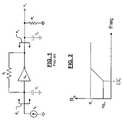
- FIG. 1is an electrical schematic of a transimpedance amplifier circuit according to the prior art
- FIG. 2is a graph illustrating output impedance as a function of frequency for the amplifier circuit of FIG. 1 ;
- FIG. 3is an electrical schematic of a transistor with parasitic capacitances according to the prior art
- FIG. 4is a graph illustrating input impedance as a function of frequency for the amplifier of FIG. 1 ;
- FIG. 5is an electrical schematic illustrating the output resistance of the transistor of FIG. 3 ;
- FIG. 6is the amplifier circuit of FIG. 1 in an open loop response configuration
- FIG. 7illustrates the open loop response of the circuit shown in FIG. 6 ;
- FIG. 8is an electrical schematic of an amplifier circuit according to one embodiment of the present invention.
- FIG. 9is an electrical schematic of a differential circuit implementation of the circuit of FIG. 8 ;
- FIG. 10is a graph illustrating input impedance as a function of frequency for the differential circuit of FIG. 9 ;
- FIG. 11illustrates the open loop response of the differential circuit of FIG. 9 ;
- FIG. 12is an electrical schematic of an amplifier circuit according to another embodiment of the present invention.
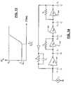
- FIG. 13is a graph illustrating the output impedance as a function of frequency for the differential circuit of FIG. 9 ;
- FIG. 14is an electrical schematic of an amplifier circuit including additional amplifier stages according to yet another embodiment of the present invention.
- FIG. 15illustrates the open loop response of the circuit of FIG. 14 ;
- FIG. 16is an electrical schematic of a differential circuit implementation using the circuit of FIG. 14 ;
- FIG. 17is a functional block diagram of the multiple amplifier circuit according to the present invention that is implemented in a read head of a disk drive system.
- FIG. 18is a functional block diagram of the multiple amplifier circuit according to the present invention that is implemented in a low noise amplifier (LNA) of a wireless device.
- LNAlow noise amplifier
- FIG. 8An amplifier circuit according to one embodiment of the present invention is illustrated in FIG. 8 and is designated by reference number 100 .
- the circuit 100includes a first amplifier 102 having a transconductance g m1 and a second amplifier 104 having a transconductance g m2 .
- the first and second amplifiers 102 , 104are connected in series. Specifically, an output 108 of the first amplifier 102 is coupled to an input 110 of the second amplifier 104 .
- An output 112 of the second amplifier 104is coupled to an input 114 of the first amplifier 102 through a feedback circuit 116 .
- the feedback circuit 116includes a feedback resistance R f and an inverter 106 .
- the inverter 106has a gain equal to ⁇ 1, although other gain values can be used.
- a resistance R 2is coupled in parallel with the second amplifier 104 .
- Also shown in FIG. 8are parasitic capacitances C 1 , C 2 , and C 3 .
- An input current source I in 126is coupled to the input terminal 114 of the first amplifier 102 .
- a load resistance R Lis coupled to the output terminal 112 of the second amplifier 104 .
- g m1is preferably greater than g m2 .
- the amplifiers 102 , 104can be inverting CMOS amplifiers (although other transistor types may be used), and the parasitic capacitances C 1 and C 2 are preferably much larger than the parasitic capacitance C 3 .
- the differential circuit 200includes a first set of amplifiers 202 , 204 connected in series and having transconductances g m1 and g m2 , respectively.
- a second set of amplifiers 206 , 208are connected in series and have transconductances g m1 and g m2 , respectively.
- An output 210 of the first set of amplifiersis coupled to an input 212 of the second set of amplifiers through a feedback resistance R f .
- An output 214 of the second set of amplifiersis coupled to an input 216 of the first set of amplifiers through a feedback resistance R f .
- Negative feedbackis achieved by feeding the output 210 from the first set of amplifiers to the input 212 of the second set of amplifiers 206 , 208 , and vice versa.
- the overall transconductance for the differential circuit 200is greater than the amplifier circuit that is shown in FIG. 1 . Even if amplifiers 202 , 206 have the same transconductance g m as the amplifier of FIG. 1 , the overall transconductance g m-eff is the product of this transconductance multiplied by g m2 and R 2 for the circuit of FIG. 9 .
- the input impedance for the differential circuit of FIG. 9is as follows:
- R in1 g m_eff ⁇ ( 1 + Rf R L ) ⁇ 1 g m2 ⁇ g m1 ⁇ R 2 ⁇ ( 1 + Rf 1 / g m ) ⁇ 1 g m2 ⁇ g m1 ⁇ R 2 + R f ⁇ g m1 ⁇ R 2
- R Lis not shunted because the parasitic capacitance C 3 is relatively low. Therefore, the differential circuit 200 is capable of higher frequency operation than the amplifier circuit of FIG. 1 .
- the input impedanceis shown as a function of frequency.
- the input impedanceis relatively flat or constant to a higher frequency
- the value of the feedback resistance R fcan be increased as desired for increased gain because this resistance R f is not limited by the output impedance as in FIG. 1 .
- the output impedance of the amplifier circuits shown in FIGS. 8 and 9is also increased because the second amplifier 104 has a low transconductance g m2 and a high output impedance.
- the overall output impedanceis not limited by the second amplifier 104 , and is merely limited by the load impedance R L .
- the noise of the amplifier circuits 100 , 200is similar to the amplifier circuit of FIG. 1 because the noise of the first amplifier 102 dominates the overall noise for the circuit, and the noise generated by the second amplifier 104 is divided by g m1 .
- the open loop response of the differential circuit of FIG. 9is illustrated using the open loop response technique described above.
- the capacitor C 1is effectively an open circuit and the input impedance is high, so the DC gain of the open loop response is equal to g m1 ⁇ R 2 .
- There is a dominant pole at DCthe capacitor C 1 is effectively an open circuit and the input impedance is high, so the DC gain of the open loop response is equal to g m1 ⁇ R 2 .
- the crossover frequencyis determined by the resistance R 2 rather than the load impedance R L . Therefore, the resistance R 2 can be increased to increase bandwidth. Further, the crossover frequency is a function of one capacitor C 1 not two. Thus, given the same transconductance g m1 as the circuit of FIG. 1 , the bandwidth of the differential circuit 200 will be greater. However, there are two nondominant poles at
- a capacitor C zcan be coupled in parallel across the feedback resistance R f in the differential mode, as shown in the half-circuit illustrated in FIG. 12 .
- the capacitor C 2adds a zero at a frequency of
- the transconductance g m1is noise dependent and is typically set to a level corresponding to minimal noise. Therefore, the transconductance g m1 cannot be further increased to further enhance the bandwidth of the differential circuit 200 .
- the feedback resistance R fis set by the input impedance R in , so those two variables are generally fixed. As the resistance R 2 is increased to increase bandwidth, at some point the output impedance is affected. This is illustrated in FIG. 13 , where it can be seen that the output impedance R o of the differential circuit 200 is relatively constant or flat up to a frequency of approximately
- FIG. 14another embodiment of an amplifier circuit is shown that mitigates the problems described above by increasing the transconductance g m2 of the second amplifier 104 , adding amplifiers 150 , 152 , and reducing the resistance R 2 .
- the transconductance of the amplifier 104is approximately one-quarter of the amplifier 102 .
- the transconductance of amplifiers 150 , 152are approximately one-twelfth of amplifier 102 .
- the term approximatelymeans within +/ ⁇ 0.25% of the designated value.
- the open loop response of the circuit of FIG. 14is illustrated using the open loop response technique.
- three nondominant polesoccur at very high frequencies due to fact that the parasitic capacitances C 3 , C 4 , and C 5 have a relatively low value.
- the lowest nondominant polealso occurs at a relatively high frequency since the resistance R 2 has a relatively low value.
- the crossover frequencynote that the transconductance g m1 is fixed for noise purposes, the feedback resistance R f is fixed by the input impedance R in , capacitor C 1 is fixed, and the resistance R 2 is set low for bandwidth purposes.
- transconductances g m3 and g m4can be adjusted to further increase bandwidth.
- the circuit of FIG. 14provides even greater flexibility in achieving a high gain, high bandwidth amplifier with other desirable circuit characteristics.
- FIG. 16a differential embodiment of the circuit of FIG. 14 is illustrated. Note that the parasitic capacitances have been omitted in FIG. 16 .
- the multiple amplifier circuit 200may be any of the multiple amplifier circuits shown in FIGS. 8-16 .
- the multiple amplifier circuit 200 according to the present inventionis implemented in a read head 202 of a disk drive system 204 .
- the multiple amplifier circuit 200is implemented in a low noise amplifier (LNA) 210 of a wireless device 212 .
- the wireless device 212may be compliant with Bluetooth networks, cellular networks, and/or Ethernet networks such as 802.11a, 802.11b, 802.11n, 802.11g, 802.16 and/or other present and future wireless standards.
- the resistance and capacitancescan be implemented in a wide variety of ways including but not limited to discrete elements such as resistors and capacitors, nonlinear variable resistors and capacitors, and/or transistor-based resistances and capacitances. Still other variations are contemplated.
Landscapes
- Engineering & Computer Science (AREA)
- Power Engineering (AREA)
- Amplifiers (AREA)
Abstract
Description
For many implementations, Rfis much larger than
such that the gain is essentially equal to —Rf.
Thus, the input impedance Rinis a function of the load resistance RL, as well as the feedback resistance Rfand the transconductance gm. The output impedance Rois equal to
at low frequency. However, due to parasitic capacitance C1, the output impedance increases to the value of the feedback resistance Rffor frequencies greater than
as is illustrated generally in
the noise at the input of the amplifier circuit is:
Thus, the noise is independent of the feedback resistance Rfand the load resistance RL, and inversely related to the transconductance gm. Note that K is Boltzmann's constant and T is temperature. Therefore, reducing noise generally involves increasing the transconductance gm.
and the noise is equal to
Accordingly, adjusting the noise level will affect the input impedance and vice versa in differential TIAs.
Where W is width, L is length, and I is current. To increase the transconductance gm, the width W of the device and/or the current I can be increased. As can be seen from the following equations, however, the width W is proportional to the parasitic capacitances C1and C2:
C1=CoxWL; and
C2ocW.
Where Coxis oxide capacitance. Thus, increasing the width W to increase the transconductance gmalso increases the parasitic capacitances C1and C2. The effects of the larger parasitic capacitances on circuit performance (specifically input impedance, gain, and bandwidth) are discussed further below.
At even higher frequencies, the input impedance may drop off due to circuit performance, as shown in
Where T represents a constant typically having a value of about 100 and L represents the length of the device. Therefore, given a value for
of 5 ohms and a device length of 0.25 microns, rowill be approximately 125 ohms. Assuming the load impedance RLis infinite, the equation for input impedance Rinis:
If an input impedance of 50 ohms is used, the feedback resistance Rfis limited to approximately 1125 ohms.
Multiplying the DC gain of the open loop response with P1provides a crossover frequency of
Further the circuit arrangement has a non-dominant pole at
which relates to a barrier frequency or maximum achievable bandwidth. Increasing the transconductance gmincreases the parasitic capacitances C1, C2. If the load impedance RLis less than the feedback resistance Rf, then the second component of the equation
is less than unity. Thus, it should be understood that there is a maximum bandwidth that can be obtained, which is basically
which limits the speed of the circuit.
Therefore, the overall transconductance for the
Note that, in this embodiment, RLis not shunted because the parasitic capacitance C3is relatively low. Therefore, the
as compared to the input impedance for the circuit of
and the crossover frequency is
These poles set an upper limit on the differential circuit's bandwidth.
as shown in
Roincreases. Therefore, by increasing the resistance R2, one of the nondominant poles moves down in frequency, which limits bandwidth. For all of these reasons, the resistance R2generally cannot be increased without restraint.
Claims (10)
Priority Applications (7)
| Application Number | Priority Date | Filing Date | Title |
|---|---|---|---|
| US10/792,619US7276969B1 (en) | 2004-03-03 | 2004-03-03 | Multi-amplifier circuit |
| US11/504,348US7312659B1 (en) | 2004-03-03 | 2006-08-15 | Multi-amplifier circuit |
| US11/904,541US7535301B1 (en) | 2004-03-03 | 2007-09-27 | Multi-amplifier circuit |
| US11/904,365US7471149B1 (en) | 2004-03-03 | 2007-09-27 | Multi-amplifier circuit |
| US11/904,765US7501890B1 (en) | 2004-03-03 | 2007-09-28 | Multi-amplifier circuit |
| US12/004,126US7468633B1 (en) | 2004-03-03 | 2007-12-20 | Multi-amplifier circuit |
| US12/286,772US7688141B1 (en) | 2004-03-03 | 2008-10-02 | Multi-amplifier circuit |
Applications Claiming Priority (1)
| Application Number | Priority Date | Filing Date | Title |
|---|---|---|---|
| US10/792,619US7276969B1 (en) | 2004-03-03 | 2004-03-03 | Multi-amplifier circuit |
Related Child Applications (4)
| Application Number | Title | Priority Date | Filing Date |
|---|---|---|---|
| US11/504,348Continuation-In-PartUS7312659B1 (en) | 2004-03-03 | 2006-08-15 | Multi-amplifier circuit |
| US11/904,365DivisionUS7471149B1 (en) | 2004-03-03 | 2007-09-27 | Multi-amplifier circuit |
| US11/904,541DivisionUS7535301B1 (en) | 2004-03-03 | 2007-09-27 | Multi-amplifier circuit |
| US11/904,765ContinuationUS7501890B1 (en) | 2004-03-03 | 2007-09-28 | Multi-amplifier circuit |
Publications (1)
| Publication Number | Publication Date |
|---|---|
| US7276969B1true US7276969B1 (en) | 2007-10-02 |
Family
ID=38535800
Family Applications (7)
| Application Number | Title | Priority Date | Filing Date |
|---|---|---|---|
| US10/792,619Expired - LifetimeUS7276969B1 (en) | 2004-03-03 | 2004-03-03 | Multi-amplifier circuit |
| US11/504,348Expired - Fee RelatedUS7312659B1 (en) | 2004-03-03 | 2006-08-15 | Multi-amplifier circuit |
| US11/904,365Expired - Fee RelatedUS7471149B1 (en) | 2004-03-03 | 2007-09-27 | Multi-amplifier circuit |
| US11/904,541Expired - Fee RelatedUS7535301B1 (en) | 2004-03-03 | 2007-09-27 | Multi-amplifier circuit |
| US11/904,765Expired - LifetimeUS7501890B1 (en) | 2004-03-03 | 2007-09-28 | Multi-amplifier circuit |
| US12/004,126Expired - Fee RelatedUS7468633B1 (en) | 2004-03-03 | 2007-12-20 | Multi-amplifier circuit |
| US12/286,772Expired - LifetimeUS7688141B1 (en) | 2004-03-03 | 2008-10-02 | Multi-amplifier circuit |
Family Applications After (6)
| Application Number | Title | Priority Date | Filing Date |
|---|---|---|---|
| US11/504,348Expired - Fee RelatedUS7312659B1 (en) | 2004-03-03 | 2006-08-15 | Multi-amplifier circuit |
| US11/904,365Expired - Fee RelatedUS7471149B1 (en) | 2004-03-03 | 2007-09-27 | Multi-amplifier circuit |
| US11/904,541Expired - Fee RelatedUS7535301B1 (en) | 2004-03-03 | 2007-09-27 | Multi-amplifier circuit |
| US11/904,765Expired - LifetimeUS7501890B1 (en) | 2004-03-03 | 2007-09-28 | Multi-amplifier circuit |
| US12/004,126Expired - Fee RelatedUS7468633B1 (en) | 2004-03-03 | 2007-12-20 | Multi-amplifier circuit |
| US12/286,772Expired - LifetimeUS7688141B1 (en) | 2004-03-03 | 2008-10-02 | Multi-amplifier circuit |
Country Status (1)
| Country | Link |
|---|---|
| US (7) | US7276969B1 (en) |
Cited By (6)
| Publication number | Priority date | Publication date | Assignee | Title |
|---|---|---|---|---|
| US7372329B1 (en)* | 2006-02-08 | 2008-05-13 | Marvell International Ltd. | Method and apparatus to remove the DC component of a feedback signal |
| US7688141B1 (en) | 2004-03-03 | 2010-03-30 | Marvell International Ltd. | Multi-amplifier circuit |
| US20100158277A1 (en)* | 2008-12-19 | 2010-06-24 | Electronics And Telecommunications Research Institute | Read-out circuit with high input impedance |
| US20120105025A1 (en)* | 2010-10-27 | 2012-05-03 | Huawei Technologies Co., Ltd. | Frequency compensation circuit for voltage regulator |
| US8872592B2 (en)* | 2012-06-19 | 2014-10-28 | Taiwan Semiconductor Manufacturing Company, Ltd. | High-speed transimpedance amplifier |
| US20160142082A1 (en)* | 2014-11-18 | 2016-05-19 | Mediatek Inc. | Signal receiving apparatus and signal receiving method |
Families Citing this family (5)
| Publication number | Priority date | Publication date | Assignee | Title |
|---|---|---|---|---|
| US8081032B1 (en) | 2006-09-26 | 2011-12-20 | Project Ft, Inc. | Broadband LNA with filter |
| US8217637B2 (en)* | 2008-01-07 | 2012-07-10 | The Hong Kong University Of Science And Technology | Frequency compensation based on dual signal paths for voltage-mode switching regulators |
| CN104205626A (en)* | 2012-04-25 | 2014-12-10 | 惠普发展公司,有限责任合伙企业 | Open-gain trans-impedance amplifier with programmable input impedance |
| WO2015196160A1 (en) | 2014-06-19 | 2015-12-23 | Project Ft, Inc. | Memoryless active device which traps even harmonic signals |
| US12028057B2 (en)* | 2022-09-23 | 2024-07-02 | Qualcomm Incorporated | Receivers for high density and low latency chip-to-chip links |
Citations (8)
| Publication number | Priority date | Publication date | Assignee | Title |
|---|---|---|---|---|
| US5220686A (en)* | 1989-04-21 | 1993-06-15 | U.S. Philips Corporation | Tunable resonance amplifier |
| US5225790A (en)* | 1992-02-28 | 1993-07-06 | Digital Equipment Corporation | Tunable wideband active filter |
| US6121831A (en)* | 1999-05-12 | 2000-09-19 | Level One Communications, Inc. | Apparatus and method for removing offset in a gain circuit |
| US6201442B1 (en)* | 1995-03-29 | 2001-03-13 | Anthony Michael James | Amplifying circuit |
| US6466091B1 (en) | 2000-10-02 | 2002-10-15 | Cirrus Logic, Inc. | High order multi-path operational amplifier with reduced input referred offset |
| US6515540B1 (en) | 2001-12-10 | 2003-02-04 | Cirrus Logic, Inc. | High order multi-path operational amplifier with output saturation recovery |
| US6525589B1 (en) | 2000-07-05 | 2003-02-25 | Cirrus Logic, Inc. | Application of a conditionally stable instrumentation amplifier to industrial measurement |
| US6657487B2 (en)* | 2001-02-05 | 2003-12-02 | Em(Us) Design, Inc | Photodetector preamplifier circuit having a rotating input stage |
Family Cites Families (4)
| Publication number | Priority date | Publication date | Assignee | Title |
|---|---|---|---|---|
| US5734294A (en)* | 1996-02-15 | 1998-03-31 | Raytheon Company | Large swing wide band high order programmable active filters |
| US7276965B1 (en)* | 2001-03-13 | 2007-10-02 | Marvell International Ltd. | Nested transimpedance amplifier |
| US7002409B1 (en) | 2004-02-11 | 2006-02-21 | Marvell International Ltd. | Compensation circuit for amplifiers having multiple stages |
| US7276969B1 (en) | 2004-03-03 | 2007-10-02 | Marvell International Ltd | Multi-amplifier circuit |
- 2004
- 2004-03-03USUS10/792,619patent/US7276969B1/ennot_activeExpired - Lifetime
- 2006
- 2006-08-15USUS11/504,348patent/US7312659B1/ennot_activeExpired - Fee Related
- 2007
- 2007-09-27USUS11/904,365patent/US7471149B1/ennot_activeExpired - Fee Related
- 2007-09-27USUS11/904,541patent/US7535301B1/ennot_activeExpired - Fee Related
- 2007-09-28USUS11/904,765patent/US7501890B1/ennot_activeExpired - Lifetime
- 2007-12-20USUS12/004,126patent/US7468633B1/ennot_activeExpired - Fee Related
- 2008
- 2008-10-02USUS12/286,772patent/US7688141B1/ennot_activeExpired - Lifetime
Patent Citations (8)
| Publication number | Priority date | Publication date | Assignee | Title |
|---|---|---|---|---|
| US5220686A (en)* | 1989-04-21 | 1993-06-15 | U.S. Philips Corporation | Tunable resonance amplifier |
| US5225790A (en)* | 1992-02-28 | 1993-07-06 | Digital Equipment Corporation | Tunable wideband active filter |
| US6201442B1 (en)* | 1995-03-29 | 2001-03-13 | Anthony Michael James | Amplifying circuit |
| US6121831A (en)* | 1999-05-12 | 2000-09-19 | Level One Communications, Inc. | Apparatus and method for removing offset in a gain circuit |
| US6525589B1 (en) | 2000-07-05 | 2003-02-25 | Cirrus Logic, Inc. | Application of a conditionally stable instrumentation amplifier to industrial measurement |
| US6466091B1 (en) | 2000-10-02 | 2002-10-15 | Cirrus Logic, Inc. | High order multi-path operational amplifier with reduced input referred offset |
| US6657487B2 (en)* | 2001-02-05 | 2003-12-02 | Em(Us) Design, Inc | Photodetector preamplifier circuit having a rotating input stage |
| US6515540B1 (en) | 2001-12-10 | 2003-02-04 | Cirrus Logic, Inc. | High order multi-path operational amplifier with output saturation recovery |
Non-Patent Citations (10)
| Title |
|---|
| Axel Thomsen, Dan Kasha, Wai Lee, Crystal Semiconductor Division, Cirrus Logic, Inc., Austin, Texas; A Five Stage Chopper Stabilized Instrumentation Amplifier Using Feedforward Compensation; 1998; 4 pages. |
| Axel Thomsen, Edwin de Angel, Sherry Ziachong Wu, Aryesh Amar, Lei Wang, Wai Lee, WA 20.1 A DC Measurement IC with 130nV<SUB>pp </SUB>Noise in 10Hz; 2000 IEEE International Solid-State Circuits Conference; 9 pages. |
| Axel Thomsen, Edwin de Angel, Sherry Ziachong Wu, Aryesh Amar, Lei Wang, Wai Lee, WA 20.1 A DC Measurement IC with 130nV<SUB>pp </SUB>Noise in 10Hz; ISSCC 2000/Session 20/Oversampled Converters/ Paper WA 20.1 ISSCC 2000 Slide Supplement; 5 pages. |
| IEEE Standard 802.11a (1999 Edition; Amended 2000); Supplement to IEEE Standard for Information Technology; Telecommunications and Information Exchange Between Systems; Local and Metropolitan Area Networks; Specific Requirements; Part 11: Wireless LAN Medium Access Control (MAC) and Physical Layer (PHY) Specifications; High-Speed Physical Layer in the 5 GHz Band, pp. 1-91. |
| IEEE Standard 802.11b (Sep. 16, 1999 Edition) Supplement to IEEE Standard for Information Technology; Telecommunications and Information Exchange Between Systems; Local and Metropolitan Area Networks; Specific Requirements; Part 11: Wireless LAN Medium Access Control (MAC) and Physical Layer (PHY) Specifications; Higher-Speed Physical Layer Extension ni the 2.4 GHz Band, pp. 1-96. |
| IEEE Standard 802.16-2001, IEEE Standard for Local and metropolitan area networks, Part 16: Air Interface for Fixed Broadband Wireless Access Systems, pp. 1-349. |
| IEEE Standard P802.11g, Draft Supplement to Standard for Information technology-Telecommunications and information exchange between systems- Local and metropolitan area networks-Specific requirements, Part 11: Wireless LAN Medium Access Control (MAC) and Physical Layer (PHY) specifications: Further Higher Data Rate Extension in the 2.4 GHz Band, Apr. 2003, pp. 1-69. |
| M. Moyal, M. Groepl, H. Werker, G. Mitteregger, J. Schambacher; Xignal Technologies AG, Munich, Germany; 23.6 A 700/900mW/Channel CMOS Dual Analog Front-End IC for VDSL with Integrated 11.5/14.5dBm Line Drivers; 2003 IEEE International Solid-State Circuits Conference; ISSCC 2003/Session 23/Mixed-Signal and Wireline Techniques; 10 pages. |
| M. Moyal, M. Groepl, H. Werker, G. Mitteregger, J. Schambacher; Xignal Technologies AG, Munich, Germany; A 700/900mW/Channel CMOS Dual Analog Front-End IC for VDSL with Integrated 11.5/14.5dBm Line Drivers; Outline, Overview 24 pages. |
| W. Grise, Dept. of IET, Morehead State University, Morehead, KY; Application of the Operational Transconductance Amplifier (OTA) to Voltage-controlled Amplifiers and Active Filters; 10 pages. |
Cited By (11)
| Publication number | Priority date | Publication date | Assignee | Title |
|---|---|---|---|---|
| US7688141B1 (en) | 2004-03-03 | 2010-03-30 | Marvell International Ltd. | Multi-amplifier circuit |
| US7372329B1 (en)* | 2006-02-08 | 2008-05-13 | Marvell International Ltd. | Method and apparatus to remove the DC component of a feedback signal |
| US7944292B1 (en) | 2006-08-16 | 2011-05-17 | Marvell International Ltd. | Method and apparatus to remove the DC component of a feedback signal |
| US20100158277A1 (en)* | 2008-12-19 | 2010-06-24 | Electronics And Telecommunications Research Institute | Read-out circuit with high input impedance |
| US8300850B2 (en)* | 2008-12-19 | 2012-10-30 | Electronics And Telecommunications Research Institute | Read-out circuit with high input impedance |
| US20120105025A1 (en)* | 2010-10-27 | 2012-05-03 | Huawei Technologies Co., Ltd. | Frequency compensation circuit for voltage regulator |
| US8847678B2 (en)* | 2010-10-27 | 2014-09-30 | Huawei Technologies Co., Ltd. | Frequency compensation circuit for voltage regulator |
| US8872592B2 (en)* | 2012-06-19 | 2014-10-28 | Taiwan Semiconductor Manufacturing Company, Ltd. | High-speed transimpedance amplifier |
| US9509260B2 (en) | 2012-06-19 | 2016-11-29 | Taiwan Semiconductor Manufacturing Company, Ltd. | High-speed transimpedance amplifier |
| US20160142082A1 (en)* | 2014-11-18 | 2016-05-19 | Mediatek Inc. | Signal receiving apparatus and signal receiving method |
| US9590676B2 (en)* | 2014-11-18 | 2017-03-07 | Mediatek Inc. | Signal receiving apparatus and signal receiving method |
Also Published As
| Publication number | Publication date |
|---|---|
| US7312659B1 (en) | 2007-12-25 |
| US7468633B1 (en) | 2008-12-23 |
| US7501890B1 (en) | 2009-03-10 |
| US7535301B1 (en) | 2009-05-19 |
| US7471149B1 (en) | 2008-12-30 |
| US7688141B1 (en) | 2010-03-30 |
Similar Documents
| Publication | Publication Date | Title |
|---|---|---|
| US7501890B1 (en) | Multi-amplifier circuit | |
| US7633338B1 (en) | Compensation circuit for amplifiers having multiple stages | |
| US7622994B2 (en) | Bias circuit with increased power supply rejection | |
| US7633337B2 (en) | Feedback-type variable gain amplifier and method of controlling the same | |
| KR100819119B1 (en) | CMOS amplifier of filter for ultra wideband application and method | |
| US20070096820A1 (en) | Differential amplifier and active load for the same | |
| US20070069821A1 (en) | Active balun device | |
| US8319553B1 (en) | Apparatus and methods for biasing amplifiers | |
| US7023271B1 (en) | Variable-gain constant-bandwidth transimpedance amplifier | |
| US20090072905A1 (en) | Variable gain amplifier having wide gain variation and wide bandwidth | |
| US10474173B2 (en) | Voltage regulator having a phase compensation circuit | |
| WO2009155566A1 (en) | Amplifier with gain expansion stage | |
| US7663444B2 (en) | Amplifying circuit utilizing nonlinear gate capacitance for enhancing linearity and related method thereof | |
| US9912304B2 (en) | Two-input amplifier | |
| US6664853B1 (en) | Wide-bandwidth differential signal amplifier | |
| US7239202B1 (en) | Variable-gain constant-bandwidth transimpedance amplifier | |
| KR100413182B1 (en) | Linear differential amplifier | |
| US7075361B1 (en) | Frequency boosting circuit for high swing cascode biasing circuits | |
| US10812029B2 (en) | Operational amplifier | |
| US7135929B1 (en) | Bias voltage circuit with ultra low output impedance | |
| US7049891B2 (en) | Amplifier bias enhancement technique | |
| US8195104B2 (en) | Electronic amplification device with current mirror for integrated power amplifiers | |
| JP3885875B2 (en) | Equivalent inductor circuit | |
| JP4525295B2 (en) | Amplifier circuit | |
| US6914484B2 (en) | Wideband constant-gain voltage amplifier |
Legal Events
| Date | Code | Title | Description |
|---|---|---|---|
| AS | Assignment | Owner name:MARVELL INTERNATIONAL LTD., BERMUDA Free format text:ASSIGNMENT OF ASSIGNORS INTEREST;ASSIGNOR:MARVELL SEMICONDUCTOR, INC.;REEL/FRAME:015047/0843 Effective date:20040302 Owner name:MARVELL SEMICONDUCTOR, INC., CALIFORNIA Free format text:ASSIGNMENT OF ASSIGNORS INTEREST;ASSIGNOR:ARAM, FARBOD;REEL/FRAME:015047/0655 Effective date:20040302 | |
| STCF | Information on status: patent grant | Free format text:PATENTED CASE | |
| FPAY | Fee payment | Year of fee payment:4 | |
| FPAY | Fee payment | Year of fee payment:8 | |
| MAFP | Maintenance fee payment | Free format text:PAYMENT OF MAINTENANCE FEE, 12TH YEAR, LARGE ENTITY (ORIGINAL EVENT CODE: M1553); ENTITY STATUS OF PATENT OWNER: LARGE ENTITY Year of fee payment:12 | |
| AS | Assignment | Owner name:CAVIUM INTERNATIONAL, CAYMAN ISLANDS Free format text:ASSIGNMENT OF ASSIGNORS INTEREST;ASSIGNOR:MARVELL INTERNATIONAL LTD.;REEL/FRAME:052918/0001 Effective date:20191231 | |
| AS | Assignment | Owner name:MARVELL ASIA PTE, LTD., SINGAPORE Free format text:ASSIGNMENT OF ASSIGNORS INTEREST;ASSIGNOR:CAVIUM INTERNATIONAL;REEL/FRAME:053475/0001 Effective date:20191231 |