US7275577B2 - Substrate bonding machine for liquid crystal display device - Google Patents
Substrate bonding machine for liquid crystal display deviceDownload PDFInfo
- Publication number
- US7275577B2 US7275577B2US10/661,472US66147203AUS7275577B2US 7275577 B2US7275577 B2US 7275577B2US 66147203 AUS66147203 AUS 66147203AUS 7275577 B2US7275577 B2US 7275577B2
- Authority
- US
- United States
- Prior art keywords
- bonding device
- substrate bonding
- chamber unit
- lower chamber
- substrate
- Prior art date
- Legal status (The legal status is an assumption and is not a legal conclusion. Google has not performed a legal analysis and makes no representation as to the accuracy of the status listed.)
- Expired - Lifetime
Links
Images


Classifications
- G—PHYSICS
- G02—OPTICS
- G02F—OPTICAL DEVICES OR ARRANGEMENTS FOR THE CONTROL OF LIGHT BY MODIFICATION OF THE OPTICAL PROPERTIES OF THE MEDIA OF THE ELEMENTS INVOLVED THEREIN; NON-LINEAR OPTICS; FREQUENCY-CHANGING OF LIGHT; OPTICAL LOGIC ELEMENTS; OPTICAL ANALOGUE/DIGITAL CONVERTERS
- G02F1/00—Devices or arrangements for the control of the intensity, colour, phase, polarisation or direction of light arriving from an independent light source, e.g. switching, gating or modulating; Non-linear optics
- G02F1/01—Devices or arrangements for the control of the intensity, colour, phase, polarisation or direction of light arriving from an independent light source, e.g. switching, gating or modulating; Non-linear optics for the control of the intensity, phase, polarisation or colour
- G02F1/13—Devices or arrangements for the control of the intensity, colour, phase, polarisation or direction of light arriving from an independent light source, e.g. switching, gating or modulating; Non-linear optics for the control of the intensity, phase, polarisation or colour based on liquid crystals, e.g. single liquid crystal display cells
- G02F1/133—Constructional arrangements; Operation of liquid crystal cells; Circuit arrangements
- G02F1/1333—Constructional arrangements; Manufacturing methods
- B—PERFORMING OPERATIONS; TRANSPORTING
- B32—LAYERED PRODUCTS
- B32B—LAYERED PRODUCTS, i.e. PRODUCTS BUILT-UP OF STRATA OF FLAT OR NON-FLAT, e.g. CELLULAR OR HONEYCOMB, FORM
- B32B37/00—Methods or apparatus for laminating, e.g. by curing or by ultrasonic bonding
- B32B37/14—Methods or apparatus for laminating, e.g. by curing or by ultrasonic bonding characterised by the properties of the layers
- B32B37/26—Methods or apparatus for laminating, e.g. by curing or by ultrasonic bonding characterised by the properties of the layers with at least one layer which influences the bonding during the lamination process, e.g. release layers or pressure equalising layers
- B—PERFORMING OPERATIONS; TRANSPORTING
- B32—LAYERED PRODUCTS
- B32B—LAYERED PRODUCTS, i.e. PRODUCTS BUILT-UP OF STRATA OF FLAT OR NON-FLAT, e.g. CELLULAR OR HONEYCOMB, FORM
- B32B38/00—Ancillary operations in connection with laminating processes
- B32B38/18—Handling of layers or the laminate
- B32B38/1825—Handling of layers or the laminate characterised by the control or constructional features of devices for tensioning, stretching or registration
- B32B38/1833—Positioning, e.g. registration or centering
- B—PERFORMING OPERATIONS; TRANSPORTING
- B32—LAYERED PRODUCTS
- B32B—LAYERED PRODUCTS, i.e. PRODUCTS BUILT-UP OF STRATA OF FLAT OR NON-FLAT, e.g. CELLULAR OR HONEYCOMB, FORM
- B32B2309/00—Parameters for the laminating or treatment process; Apparatus details
- B32B2309/60—In a particular environment
- B32B2309/65—Dust free, e.g. clean room
- B—PERFORMING OPERATIONS; TRANSPORTING
- B32—LAYERED PRODUCTS
- B32B—LAYERED PRODUCTS, i.e. PRODUCTS BUILT-UP OF STRATA OF FLAT OR NON-FLAT, e.g. CELLULAR OR HONEYCOMB, FORM
- B32B2309/00—Parameters for the laminating or treatment process; Apparatus details
- B32B2309/60—In a particular environment
- B32B2309/68—Vacuum
- B—PERFORMING OPERATIONS; TRANSPORTING
- B32—LAYERED PRODUCTS
- B32B—LAYERED PRODUCTS, i.e. PRODUCTS BUILT-UP OF STRATA OF FLAT OR NON-FLAT, e.g. CELLULAR OR HONEYCOMB, FORM
- B32B2457/00—Electrical equipment
- B32B2457/20—Displays, e.g. liquid crystal displays, plasma displays
- B—PERFORMING OPERATIONS; TRANSPORTING
- B32—LAYERED PRODUCTS
- B32B—LAYERED PRODUCTS, i.e. PRODUCTS BUILT-UP OF STRATA OF FLAT OR NON-FLAT, e.g. CELLULAR OR HONEYCOMB, FORM
- B32B2457/00—Electrical equipment
- B32B2457/20—Displays, e.g. liquid crystal displays, plasma displays
- B32B2457/202—LCD, i.e. liquid crystal displays
- B—PERFORMING OPERATIONS; TRANSPORTING
- B32—LAYERED PRODUCTS
- B32B—LAYERED PRODUCTS, i.e. PRODUCTS BUILT-UP OF STRATA OF FLAT OR NON-FLAT, e.g. CELLULAR OR HONEYCOMB, FORM
- B32B38/00—Ancillary operations in connection with laminating processes
- B32B38/18—Handling of layers or the laminate
- B32B38/1858—Handling of layers or the laminate using vacuum
- G—PHYSICS
- G02—OPTICS
- G02F—OPTICAL DEVICES OR ARRANGEMENTS FOR THE CONTROL OF LIGHT BY MODIFICATION OF THE OPTICAL PROPERTIES OF THE MEDIA OF THE ELEMENTS INVOLVED THEREIN; NON-LINEAR OPTICS; FREQUENCY-CHANGING OF LIGHT; OPTICAL LOGIC ELEMENTS; OPTICAL ANALOGUE/DIGITAL CONVERTERS
- G02F1/00—Devices or arrangements for the control of the intensity, colour, phase, polarisation or direction of light arriving from an independent light source, e.g. switching, gating or modulating; Non-linear optics
- G02F1/01—Devices or arrangements for the control of the intensity, colour, phase, polarisation or direction of light arriving from an independent light source, e.g. switching, gating or modulating; Non-linear optics for the control of the intensity, phase, polarisation or colour
- G02F1/13—Devices or arrangements for the control of the intensity, colour, phase, polarisation or direction of light arriving from an independent light source, e.g. switching, gating or modulating; Non-linear optics for the control of the intensity, phase, polarisation or colour based on liquid crystals, e.g. single liquid crystal display cells
- G02F1/133—Constructional arrangements; Operation of liquid crystal cells; Circuit arrangements
- G02F1/1333—Constructional arrangements; Manufacturing methods
- G02F1/133354—Arrangements for aligning or assembling substrates
Definitions
- the present inventionrelates to liquid crystal display (LCD) devices, and more particularly to a substrate bonding device facilitating the fabrication of large-sized LCD devices.
- LCDliquid crystal display
- LCDliquid crystal displays
- PDPplasma displays
- ELDelectro luminescent displays
- VFDvacuum fluorescent displays
- LCD deviceshaving excellent display quality, light weight, thin dimensions, and consuming low amounts of power, have been very widely used.
- LCD technologyhas already replaced cathode ray tubes (CRT) as the display of choice.
- CTRcathode ray tubes
- LCD devicescapable of expressing high quality images (e.g., images having a high resolution and a high luminance) with large-sized screens, while still maintaining a light weight, minimal dimensions, and low power consumption must be developed.
- high quality imagese.g., images having a high resolution and a high luminance
- LCDsare generally fabricated by coating a patterned sealant material onto one of two substrates, providing the patterned sealant material with an injection hole, bonding the two substrates together in a vacuum, and injecting liquid crystal material through the injection hole and into a space between the two bonded substrates. It has also been suggested that the liquid crystal material may be provided to LCDs via a dispensing method, rather than an injection method.
- Japanese Laid Open Patent Nos. 2000-284295 and 2001-005405can be understood to disclose a method of dispensing liquid crystal material wherein, after liquid crystal material is dispensed and sealant material is coated onto one of the two substrates, the other of the two substrates is bonded to the one substrate in a vacuum.
- liquid crystal material dispensing methodsare advantageous over liquid crystal material injection methods because they reduce the number of fabrication steps required to fabricate LCD panels (e.g., formation of the liquid crystal injection hole, injection of the liquid crystal material, sealing of the liquid crystal injection hole, etc., are omitted), thereby simplifying fabrication of LCD panels. Accordingly, fabricating LCD panels by dispensing liquid crystal material have been the subject of recent research.
- FIGS. 1 and 2illustrate a related art substrate bonding device used in fabricating LCD panels formed with dispensed liquid crystal material.
- the related art LCD device substrate bonding deviceis provided with a frame 10 , an upper stage 21 , a lower stage 22 , a sealant dispensing part (not shown), a liquid crystal material dispensing part 30 , an upper chamber unit 31 , a lower chamber unit 32 , chamber moving means, and stage moving means.
- the sealant dispensing part (not shown) and liquid crystal dispensing part 30are typically provided at a side portion of the frame 10 . Moreover, the upper and lower chamber units 31 and 32 , respectively, can be joined to each other to bond substrates of an LCD panel.
- the chamber moving meansgenerally includes a driving motor 40 for moving the lower chamber unit 32 laterally to predetermined positions where the substrates are to be bonded (S 2 ) and where the sealant material is to be coated and where the liquid crystal material is to be dispensed (S 1 ).
- the stage moving meansincludes a driving motor 50 for raising and lowering the upper stage 21 to predetermined positions.
- a first substrate 51is positioned on the lower stage 22 of the lower chamber unit 32 and the chamber moving means 40 moves the lower chamber unit 32 under the upper chamber unit 31 such that the lower stage 22 is beneath the upper stage 21 .
- the driving motor 50 of the stage moving meanslowers the upper stage 21 to a predetermined position such that the first substrate 51 is secured to the lowered upper stage 21 .
- the upper stage 21to which the first substrate 51 is secured, is raised to a predetermined position.
- the chamber moving means 40then moves the lower chamber unit 32 to a position where a second substrate 52 is loaded on the lower stage 22 .
- the chamber moving means 40moves the lower chamber unit 32 to a first predetermined position S 1 (as shown in FIG. 1 ).
- sealant material coating and liquid crystal material dispensing processesare applied to the second substrate 52 using the sealant dispensing part (not shown) and the liquid crystal dispensing part 30 , respectively.
- the chamber moving means 40moves the lower chamber unit 32 to a second predetermined position S 2 (as shown in FIG. 2 ) where the first and second substrates 51 and 52 , respectively, can be bonded together.
- the upper and lower chamber units 31 and 32are joined to each other such that the upper and lower stages 21 and 22 , respectively, are arranged within an enclosed space.
- a vacuumis then created within the enclosed space using an evacuating means (not shown).
- the stage moving means 50lowers the upper stage 21 such that the first substrate 51 , secured to the upper stage 21 , contacts the second substrate 52 on the lower stage 22 .
- the upper stage 21is lowered until the two substrates become bonded, thereby completing the fabrication of the LCD panel.
- the related art bonding devicemay increases the overall amount of time required to fabricate one LCD panel. More specifically, because liquid crystal material is dispensed, sealant material is coated, and substrates are bonded all using the same apparatus, substrates transported from preceding processes must stand idle until the processes performed by the related art substrate bonding device are complete. Moreover, the overall productivity of the LCD fabrication process is reduced since the related art substrate bonding device cannot process material transported thereto while other fabrication processes are in progress.
- an imperfect sealcan be formed between the joined upper and lower chamber units 31 and 32 , respectively.
- airmay leak from the external environment into the enclosed space defined by the upper and lower chamber units and the substrates may become damaged during bonding, thereby creating a defective bond.
- the many positions the lower chamber 32is required to move to (e.g., the first position S 1 for dispensing the liquid crystal and coating the sealant material onto the second substrate 52 , the second position S 2 for bonding the two substrates, etc.) prevent the substrates from being properly aligned for a successful bonding.
- the present inventionis directed to a substrate bonding device for a liquid crystal display device that substantially obviates one or more of the problems due to limitations and disadvantages of the related art.
- An advantage of the present inventionprovides a substrate bonding device for use in fabricating an LCD device that can reduce the overall time required to fabricate LCDs while enabling accurate and simple alignment of substrates.
- Another advantage of the present inventionprovides a substrate bonding device for use in fabricating an LCD device that enables easy monitoring of a substrate bonding process and a progression of continuous substrate bonding.
- Yet another advantage of the present inventionprovides a substrate bonding device for use in fabricating an LCD device that substantially prevents the introduction of foreign material into a region of the substrate bonding device where the substrates are bonded together, prevents generation of static electricity around the substrates, and promotes smooth bonding processes.
- Still another advantage of the present inventionprovides a substrate bonding device for use in fabricating an LCD device that can substantially prevent fine particles from sticking to surfaces of the stages and that can substantially prevent the generation of defects within the LCD caused by foreign material introduced during a substrate bonding process.
- a substrate bonding devicemay, for example, include a base frame for providing an outer appearance; a lower chamber unit mounted to the base frame; an upper chamber unit positioned over the lower chamber unit and joinable to the lower chamber unit; chamber moving means mounted to the base frame for raising and lowering the upper chamber unit; an upper stage and a lower stage provided within interior spaces of the upper and lower chamber units, respectively, for securing a first substrate and a second substrate, respectively; alignment cameras provided to at least one of the upper and lower chamber units for verifying an alignment state of alignment marks formed on the first and second substrates; and alignment means provided to side surfaces of the lower chamber unit for adjusting relative positions of the first and second substrates.
- a substrate bonding devicemay, for example, include a base frame for providing an outer appearance; a lower chamber unit mounted to the base frame; an upper chamber unit positioned over the lower chamber unit and joinable to the lower chamber unit; chamber moving means mounted to the base frame for raising and lowering the upper chamber unit; an upper stage and a lower stage provided within interior spaces of the upper and lower chamber units, respectively, for securing a first substrate and a second substrate, respectively; sealing means provided to at least one surface of the upper and lower chamber units; and a case for enclosing the upper and lower chamber units, the case having an side portion, wherein an opening is provided in the side portion, through which the substrates may be inserted.
- a substrate bonding devicemay, for example, include a base frame for providing an outer appearance; a lower chamber unit mounted to the base frame; an upper chamber unit positioned over the lower chamber unit and joinable to the lower chamber unit; chamber moving means mounted to the base frame for raising and lowering the upper chamber unit; an upper stage and a lower stage provided within interior spaces of the upper and lower chamber units, respectively, for securing a first substrate and a second substrate, respectively; spraying means provided along side portions of one of the upper and lower chamber units for spraying gas (e.g., nitrogen, air, etc.) toward sides of the other of the upper and lower chamber units; blowing means for blowing gas through the spraying means; and a first flow tube having a first end in communication with the spraying means and a second end in communication with the blowing means.
- gase.g., nitrogen, air, etc.
- a method of protecting stages in a substrate bonding devicemay, for example, include positioning a protection sheet over a surface of one of an upper and lower stage; verifying a time during which the protection sheet is replaced; and rotating first and second reels when the time for replacing the protection sheet is determined, wherein a used protection sheet is wound over the first reel and an unused protection sheet is wound off the second reel and over the surface of the one of the upper and lower stage.
- FIGS. 1 and 2illustrate a related art substrate bonding device for use in fabricating LCD panels formed via liquid crystal material dispensing methods
- FIG. 3illustrates a substrate bonding device for fabricating LCD panels in accordance with a first aspect of the present invention in an unloaded state
- FIGS. 4A and 4Billustrate the interior structures of stages within the substrate bonding device in accordance with the first aspect of the present invention
- FIG. 5illustrates a plan view of an arrangement of rotatable cams within the substrate bonding device in accordance with the first aspect of the present invention
- FIG. 6illustrates a perspective view of support means within the substrate bonding device in accordance with the first aspect of the present invention
- FIG. 7schematically illustrates vacuum pumps and pipelines within the substrate bonding device in accordance with the first aspect of the present invention
- FIG. 8illustrates the loading of a first substrate within the substrate bonding device in accordance with the first aspect of the present invention
- FIGS. 9 and 10illustrate the securing of a first substrate to an upper stage within the substrate bonding device in accordance with the first aspect of the present invention
- FIGS. 11 to 13illustrate the loading of a second substrate and the securing of the second substrate to a lower stage within the substrate bonding device in accordance with the first aspect of the present invention
- FIGS. 14 , 15 A, and 15 Billustrate a bonding of the substrates within the substrate bonding device in accordance with the first aspect of the present invention
- FIGS. 16 to 18illustrate the alignment of the first and second substrates using the alignment means in accordance with a first preferred embodiment of the present invention, schematically;
- FIGS. 19A and 19Billustrate the venting process within the substrate bonding device in accordance with the first aspect of the present invention
- FIG. 20illustrates a substrate bonding device for fabricating LCD panels in accordance with a second aspect of the present invention in an unloaded state
- FIG. 21illustrates the simultaneous loading of unbonded substrates into, and unloading of bonded substrates out of the substrate bonding device in accordance with the second aspect of the present invention
- FIG. 22illustrates a substrate bonding device for fabricating LCD panels in accordance with a third aspect of the present invention in an unloaded state
- FIG. 23illustrates a perspective view of spraying means within the substrate bonding device in accordance with the third aspect of the present invention.
- FIG. 24illustrates a substrate bonding device for fabricating LCD panels in accordance with a fourth aspect of the present invention in an unloaded state
- FIGS. 25 to 29illustrate the process of bonding substrates using the substrate bonding device in accordance with the fourth aspect of the present invention
- FIGS. 30 and 31illustrate key parts showing a process for positioning a protection sheet within the substrate bonding device in accordance with the fourth aspect of the present invention
- FIG. 32illustrates the principles of the third aspect of the present invention applied to the substrate bonding device in accordance with the second aspect of the present invention
- FIG. 33illustrates the principles of the fourth aspect of the present invention applied to the substrate bonding device in accordance with the second aspect of the present invention
- FIG. 34illustrates the principles of the third and fourth aspects of the present invention applied to the substrate bonding device in accordance with the second aspect of the present invention.
- FIG. 35illustrates the principles of the fourth aspect of the present invention applied to the substrate bonding device in accordance with the third aspect of the present invention.
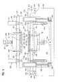
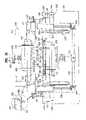
- FIG. 3illustrates a substrate bonding device for fabricating LCD panels in accordance with a first aspect of the present invention in an unloaded state.
- the substrate bonding devicein accordance with the principles of the first aspect of the present invention may, for example, include a base frame 100 ; an upper chamber unit 210 ; a lower chamber unit 220 ; chamber moving means (e.g., 310 , 320 , 330 , 340 , and 350 ); an upper stage 230 ; and a lower stage 240 ; sealing means (e.g., 250 ); alignment cameras 520 ; alignment means (e.g., 531 , 532 , 533 , 534 , 540 , and 541 ) shown, for example, in FIG. 5 ; support means (e.g., 710 and 720 ), shown for example, in FIG. 6 ; vacuum pumping means (e.g., 610 , 621 , and 622 ) shown, for example, in FIG. 7 ; and interlocking means (e.g., 510 ).
- alignment cameras 520alignment means (e.g., 531 , 532 , 533
- the base frame 100may be fixed to a supporting structure or surface (e.g., the ground), may form the exterior appearance of the substrate bonding device, and may support different components discussed in greater detail below.
- a supporting structure or surfacee.g., the ground
- upper and lower stages 230 and 240may be fixed to the upper chamber unit 210 and the lower chamber unit 220 , respectively.
- the upper and lower chamber units 210 and 220may be selectively joined to each other to define an interior space.
- the upper chamber unit 210may, for example, include an upper base 211 that may be exposed to an external environment and an upper chamber plate 212 immovably attached to a bottom surface of the periphery of the upper base 211 .
- the upper chamber plate 212may be provided as a rectangular rim and define an interior space within which the upper stage 230 is fixed. Since the upper stage 230 is fixed to the upper chamber unit 210 , the upper stage may be raised and lowered with the upper chamber unit 210 .
- a first seal member 213may be arranged between the upper base 211 and the upper chamber plate 212 of the upper chamber unit 210 to seal the interior space defined by the upper chamber plate 212 from the external environment.
- the first seal member 213may be provided as a gasket, an o-ring, or the like, suitable for sealing.
- the lower chamber unit 220may, for example, include a lower base 221 fixed to the base frame 100 and a lower chamber plate 222 arranged above a top surface of the periphery of the lower base 221 .
- the lower chamber plate 222maybe provided as a rectangular rim and define an interior space within the which the lower stage 240 is fixed.
- the lower chamber plate 222may be movable in left, right, forward, and backward (i.e., lateral) directions with respect to the lower base 221 .
- the lower chamber unit 220may include a fixing plate 223 for fixing the lower base 221 to the base frame 100 .
- a second seal member 224may be arranged between the lower base 221 and the lower chamber plate 222 of the lower chamber unit 220 and may seal the interior space defined by the lower chamber plate 222 from a the external environment.
- the second seal member 224may be provided as a gasket, an O-ring, or the like, suitable for sealing.
- At least one support part 225may be arranged between the lower base 221 and the lower chamber plate 222 for maintaining the lower chamber plate 222 a predetermined a distance from the upper surface of the lower base 221 .
- the support part 225may include a first end attached to a bottom portion of the lower chamber plate 222 and a second end that is movable in lateral directions with respect to the lower base 221 and is attached to a piece that is attached to a bottom portion of the lower base 221 . Accordingly, the support part 225 enables the lower chamber plate 222 to move in left, right, forward, and backward directions relative to the lower base 221 .
- the aforementioned chamber moving meansmay, for example, include a driving motor 310 fixed to the base frame 100 , a driving shaft 320 coupled to the driving motor 310 , a connecting shaft 330 arranged substantially perpendicular to the driving shaft 320 for receiving a driving force from the driving shaft 320 , a connecting part 340 for connecting the driving shaft 320 to the connecting shaft 330 , and a jack part 350 mounted at an end of the connecting shaft 330 .
- the driving motor 310may be arranged within an interior bottom portion of the base frame 100 and may be provided as a bilateral shaft motor, having shafts horizontally projecting from both sides of the driving motor 310 .
- the driving shaft 320may be connected to the driving motor 310 and transmit driving forces along a horizontal direction to the connecting part 340 while the connecting shaft 330 may be connected to the connecting part 340 to transmit the driving force along a vertical direction with respect to the driving shaft 320 .
- the jack part 350may be provided at the end of the connecting shaft 330 , may be connected to the upper chamber unit 210 , and may include a nut housing to move the upper chamber unit 210 upwardly and downwardly, depending on a rotation direction of rotation of the connecting shaft 330 .
- the connecting part 340may be provided as a system of bevel gears to translate a rotational force supplied from the driving shaft 320 along a horizontal direction into a vertical rotational force to the connecting shaft 330 .
- the upper and lower stages 230 and 240may each include a fixing plate 231 and 241 , respectively, fixed to a respective one of the upper chamber unit 210 and the lower chamber unit 220 ; a securing plate 232 and 242 , respectively, for securing the first and second substrates; and a plurality of fixing blocks 233 and 243 , respectively, arranged between respective pairs of the fixing plates 231 and 241 and the securing plates 232 and 242 .
- the securing plates 232 and 242may each be provided as an electrostatic chuck (ESC) formed of a material such as polyimide for securing a substrate to a respective one of the stages by applying an electrostatic charge.
- ESCelectrostatic chuck
- FIGS. 4A and 4Billustrate the interior structures of stages within the substrate bonding device in accordance with the principles of the present invention.
- FIGS. 4A and 4Billustrate enlarged sectional views of “A” and “B” regions, respectively, shown in FIG. 3 .
- each of the securing plates 232 and 242may, for example, additionally include a plurality of holes 232 a and 242 a , respectively, for transmitting a suction force to secure respective ones of the substrates.
- each of the plurality of holes 232 a and 242 amay be in communication with a respective one of a vacuum pipeline 271 and 272 , respectively, formed within a respective one of the upper stage 230 and lower stage 240 .
- each vacuum pipeline 271 and 272may be connected to a vacuum pump means (e.g., 622 , as shown in FIG. 7 ) for generating the suction force.
- the sealing means 250may be provided as an O-ring, formed of a material such as rubber, and fitted along a top surface of the lower chamber plate 222 of the lower chamber unit 220 .
- the third seal member 250may project from the top surface of the lower chamber plate 222 to a predetermined height and be formed to a predetermined thickness sufficient to prevent substrates, secured by respective ones of the upper and lower stages 230 and 240 , from becoming proximately arranged next to each other upon initially joining the upper and lower chamber units 210 and 220 , as will be discussed in greater detail below.
- the thickness of the third seal member 250may be sufficient to permit the substrates to contact each other when the third seal member 250 is compressed.
- the aforementioned alignment meansmay be used to align substrates 110 and 120 secured to upper and lower stages 230 and 240 , respectively.
- the alignment meansmay be coupled to the lower chamber unit 220 and, during alignment of the substrates 110 and 120 , the lower stage 240 may be kept substantially stationary while the position of the upper stage 230 is adjusted in accordance with the position of the lower chamber plate 222 , adjustable with the alignment means.
- the alignment meansmay, for example, include a plurality of cams 531 , 532 , 533 , and 534 and step motors 540 connected to shafts 541 for driving the cams 531 , 532 , 533 , and 534 .
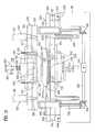
- FIG. 5illustrates a plan view of an arrangement of the rotatable cams in the substrate bonding device in accordance with the principles of the present invention.
- each of the cams 531 , 532 , 533 , and 534may be rotatably arranged to selectively contact a peripheral surface of the lower chamber plate 222 .
- the cams 531 , 532 , 533 , and 534may be arranged substantially symmetrically along each of the peripheral surfaces of the lower chamber plate 222 .
- each of the camsmay be eccentrically rotatable such that, upon rotating, the lower chamber plate 222 may be pushed in a predetermined direction.
- the lower chamber unitmay be defined by four sides, wherein a first pair of opposing sides may be longer than a second pair of opposing sides. Accordingly, two cams may be rotatably arranged to selectively contact each side of the first pair of opposing sides and one cam may be arranged to selectively contact a middle portion of each side of the second pair of opposing sides such that the lower chamber plate 222 may be movable in the left, right, forward, and backward directions.
- each of the cams 531 532 , 533 , and 534may rotate substantially in unison to push the lower chamber plate 222 along a predetermined direction.
- first cams 531are rotated to push the lower chamber plate 222 along a predetermined direction
- the second cams 532arranged opposite the first cams 531
- the third and fourth cams 533 and 534respectively, arranged adjacent the first cams 531
- a distance between surfaces of oppositely arranged camsmay remain substantially constant (e.g., the length or width of the lower chamber plate 222 ).
- the interlocking means 510may, for example, includes a plurality of holes 222 a provided in the lower chamber plates 222 of the lower chamber unit 220 , and a plurality of linear actuators 511 fixed along a periphery of the upper chamber unit 210 for lowering corresponding ones of the plurality of movable shafts 512 until the movable shafts 512 are received within respective ones of the holes 222 a.
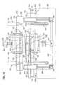
- FIG. 6illustrates a perspective view of support means within the substrate bonding device in accordance with the first aspect of the present invention.
- the support meansmay, for example, include a lift pin 710 and a plurality of actuators 720 .
- the lift pin 710may have a thickness sufficient to support at least one substrate while substantially preventing the at least one substrate from sagging.
- a central region of the lift pin 710may include a downwardly bent portion for allowing a loader 910 to support the at least one substrate without interfering with the lift pin 710 .
- portions of the lift pin 710may be raised through the lower stage 240 and above the upper surface of the lower stage 240 to facilitate the safe seating of the substrate 120 as it is loaded onto the lower stage 240 .
- a top surface of the lift pin 710may be positioned below the top surface of the lower stage 240 .
- a plurality of actuators 720may raise and lower the lift pin 710 as required. Accordingly, the support means may facilitate the unloading of the bonded and unbonded substrates seated on the lower stage 240 (see, for example FIG. 21 ).
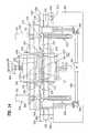
- FIG. 7schematically illustrates vacuum pumps and pipelines within the substrate bonding device in accordance with the first aspect of the present invention.
- the aforementioned vacuum pumping means 610 , 621 , and 622may be provided to at least one of the upper and lower chamber units 210 and 220 and may evacuate the sealed interior space defined by the upper and lower chamber units 210 and 220 joined together.
- the vacuum pumping means 610 , 621 , and 622may, for example, include a high vacuum pump (Turbo Molecular Pump, “TMP”) 610 and a first and second low vacuum pump (Dry-Pump) 621 and 622 , respectively.
- TMPTorbo Molecular Pump
- Dry-Pumpfirst and second low vacuum pump
- the first low vacuum pump 621may be connected to a high vacuum chamber pipeline 630 provided at a central region of the upper chamber unit 210 and enable the high vacuum pump 610 and the interior spaces defined by the upper and lower chamber plates 212 and 222 to be in communication with each other. Moreover, the first low vacuum pump may evacuate the sealed interior space, definable by the upper and lower chamber units 210 and 220 to a predetermined pressure.
- the second low vacuum pump 622may be connected to low vacuum chamber pipelines 641 and 642 passing through side regions of the upper and lower chamber units 210 and 220 . Further, the second low vacuum pump 622 may be connected to pipelines in the upper and lower stages 230 and 240 and to a substrate securing pipeline 650 connected to the vacuum pipelines 271 and 272 in the stages 230 and 240 , respectively, for securing the substrates using a suction force.
- the pipelines 630 , 641 , 642 , and 650may include at least one shut off valve 661 , 662 , 663 , 664 , 665 , 666 , 667 , 668 , and 669 .
- the high pressure vacuum pipeline 630may include a pressure sensor 670 for measuring a pressure inside of the interior spaces the substrates are held therein.
- the low vacuum chamber pipelines 641 and 642 and the substrate securing pipeline 650in communication with the second low vacuum pump 622 , may be used as pipelines for venting. Accordingly, a gas such as nitrogen (N 2 ) may be injected into the sealed interior space definable by the upper and lower chamber units 210 and 220 for returning a pressure therein from a vacuum state to an atmospheric pressure.
- a gassuch as nitrogen (N 2 ) may be injected into the sealed interior space definable by the upper and lower chamber units 210 and 220 for returning a pressure therein from a vacuum state to an atmospheric pressure.
- a plurality of alignment cameras 520may be mounted within at least one of the upper and lower chamber units 210 and 220 , respectively, such that alignment marks (not shown) formed on the substrates (not shown), secured by the upper or lower stages 230 or 240 , may be observed through at least one of the upper chamber unit 210 and the lower chamber unit 220 .
- FIGS. 8 to 19BA method for fabricating an LCD device using the substrate bonding device shown in FIGS. 3 to 7 will now be described in greater detail with reference to FIGS. 8 to 19B .
- the substrate bonding devicemay first be provided in the unloaded state as shown in FIG. 3 . Subsequently, a first substrate 110 may be brought into a space between the upper and lower chamber units 210 and 220 , respectively, via a loader 910 .
- the upper chamber unit 210may be lowered from its original position such that the upper stage 230 is arranged proximate the first substrate 110 .
- the first substrate 110may then become secured to the upper stage 230 by a suction force generated by the second low vacuum pump 622 and by an electrostatic charge (ESC) generated by the securing plate 232 .
- ESCelectrostatic charge
- the upper chamber unit 210may be raised to its original position and the loader 910 may be removed from the substrate bonding device.
- the loader 910may be re-inserted inserted into the substrate bonding device while supporting the second substrate 120 .
- the lift pin 710may be raised from its original position, through the lower stage 230 and from below the upper surface of the lower stage 230 , to push the second substrate 120 away from the loader 910 .
- the lift pin 710may support the second substrate 120 at a predetermined height above the loader 910 (as shown in FIG. 12 ).
- the loader 910may be removed from the substrate bonding device.
- the lift pin 710may be lowered such that the second substrate 120 rests on, and is supported by, the lower stage 240 .
- the second substrate 120may be secured to the lower stage 240 using suction forces and electrostatic charges.
- the first and second substrates 110 and 120are secured to their respective stages 230 and 240 , loading of the substrate bonding device is complete.
- the driving motor 310 of the chamber moving meansmay rotate the driving shafts 320 and the connecting shafts 330 to lower the jack parts 350 from their original positions.
- the upper chamber unit 210is lowered as the jack parts 350 are lowered from their original positions.
- the linear actuators 511may lower the plurality of movable shafts 512 such that the moveable shafts 512 project to a predetermined height from the bottom surface of the upper chamber plate 212 .
- the end portions of the moveable shafts 512may be received within, and contact interior surfaces of respective ones of the holes 222 a formed in the lower chamber plate 222 .
- the movable shafts 512may contact the interior surfaces of the holes 222 a in succession.
- the chamber moving meansmoves the upper chamber unit 210 downwardly such that a bottom surface of the upper chamber plate 212 contacts a top surface of the third sealing member 250 , fitted to a periphery of the lower chamber plate 222 .
- the jack parts 350are lowered further, they move out from between the upper chamber unit 210 the lower chamber unit 220 such that a sealed interior space, defined by the upper and lower chamber units 210 and 220 is created, wherein the sealed interior space is substantially sealed from the external environment due to the weight of the upper chamber unit 210 pressing upon the third seal member 250 . Therefore, the first and second substrates 110 and 120 may be substantially isolated from the external environment.
- the first and second substrates 110 and 120may be partially bonded to each other but separated from each other by an initial distance of a few hundred microns.
- the relative positions of the first and second substrates 110 and 120may be adjusted in a subsequent alignment process.
- the substratemay be bonded together in a subsequent venting process, as will be discussed in greater detail below.
- the distance between the upper chamber unit 210 and the lower chamber unit 220(and therefore the gap between the substrates) may be determined by the gap determining sensor 920 .
- the sealed interior space defined by the upper and lower chamber units 210 and 220is evacuated. Accordingly, the first and second low vacuum pumps 621 and 622 may be activated to evacuate the sealed interior space to a first pressure, measured by the pressure sensor 670 . After it is determined that the first and second low vacuum pumps 621 and 622 have evacuated the interior space to the first pressure, the high vacuum pump 610 may be activated to substantially evacuate the interior space.
- the high and first low vacuum pumps 610 and 621may be connected to the same pipeline 630 . Therefore, the first low vacuum pump 621 may be deactivated when the high vacuum pump 610 is activated.
- the first and second substrates 110 and 120arranged within the evacuated, sealed interior space may be aligned by the alignment means and the alignment cameras 520 .
- the alignment cameras 520may observe alignment marks (not shown) formed on the first and second substrates 110 and 120 and may verify positional deviations between the alignment marks on the substrates 110 and 120 .
- the verified positional deviationsmay include distances the upper stage is required to move in order to be properly aligned. Accordingly, the distances the upper stage 230 is required to move to be properly aligned may be calculated with reference to the verified deviations.
- the lower stage 240is fixed to a top surface of the lower base 221 . Accordingly, the position of the lower chamber plate 222 with respect to the lower stage 240 may be adjusted. Since the upper stage 230 does not move with respect to the upper chamber plate 212 , the upper stage 230 moves in substantial unison with the movement of the lower chamber plate 222 via the interlocking means 510 .
- the motion of the lower chamber plate 222generated by the alignment means (e.g., rotation of the cams 531 , 532 , 533 , and 534 at the peripheral surfaces of the lower chamber plate 222 ), may be translated through the interlocking means 510 to the upper stage 230 , fixed to the upper chamber unit 210 .
- the degree and direction the cams rotatemay be based on the calculated distance the upper stage is required to move to be properly aligned. Accordingly, step motors 540 , eccentrically fixed the cams via cam shafts 541 , may rotate the cams as required. According to the principles of the present invention, the cams 531 , 532 , 533 , and 534 may be rotatably arranged to selectively contact a peripheral surface of the lower chamber plate 222 .
- the upper chamber unit 210upon verifying a positional deviation between the first and second substrates 110 and 120 using the alignment cameras 520 , it may determined, for example, that the first substrate 110 has a 2 mm deviation in a rear direction and 2 mm deviation in a left direction with respect to the second substrate 120 , the upper chamber unit 210 , having the upper stage 230 fixed thereto, may then be moved by 2 mm in a front direction and 2 mm in a right direction using the aforementioned alignment means. Accordingly, the first and second substrates may be accurately aligned while they are secured by their respective stages 230 and 240 .
- the aforementioned exemplary positional deviationmay be corrected by eccentrically rotating the cams 531 , 532 , 533 , and 534 contacting the lower chamber plate 222 to a predetermined degree and in a predetermined manner.
- the first cams 531 , arranged at a rear peripheral surface of the lower chamber plate 222may be eccentrically rotated such that lower chamber plate is moved forward while the second cams 532 , arranged at a front peripheral surface of the lower chamber plate 222 , are eccentrically rotated such that the second cams 532 and the front peripheral surface of the lower chamber plate 222 are separated by a predetermined distance.
- the third cam 533arranged at the left peripheral surface of the lower chamber plate 222 , may be eccentrically rotated such that the lower chamber plate 222 is moved to the right while the fourth cam 534 , arranged at the right peripheral surface of the lower chamber plate 222 , is eccentrically rotated such that the fourth cam and the right peripheral surface of the lower chamber plate are separated by a predetermined distance.
- the principles of the present inventionmay be applied to correct substantially any positional deviation between the substrates, wherein rotational amounts and directions of individual ones of the cams may be selectively controlled to move the lower chamber plate 222 in front, rear, left, and right directions either consecutively or simultaneously (e.g., to move the lower chamber plate 222 in diagonal directions).
- the motion imparted by alignment means to the lower chamber plate 222is translated through the interlocking means 510 to the upper chamber unit.
- the first and second substrates 110 and 120are substantially aligned.
- the principles of the present inventionprovide the lower chamber plate 222 , the upper chamber unit 210 , the upper stage 230 , and the upper substrate 110 to move substantially as a single body, independent of the lower stage 240 . Therefore, a smooth and precise positional alignment of the first and second substrates, secured by their respective stages 230 and 240 , may be obtained.
- the first and substrates 110 and 120may be aligned more than once depending on the type of alignment marks that are formed on the substrates. For example, if two types of alignment marks are formed on the first and second substrates (e.g., rough alignment marks and fine alignment marks), two alignment processes may need to be performed, wherein the rough alignment marks are aligned in a rough alignment process before the fine alignment marks are aligned in a fine alignment process.
- two types of alignment marksare formed on the first and second substrates (e.g., rough alignment marks and fine alignment marks)
- two alignment processesmay need to be performed, wherein the rough alignment marks are aligned in a rough alignment process before the fine alignment marks are aligned in a fine alignment process.
- the first substrate 110may be spaced apart from the second substrate 120 by approximately 500 ⁇ m to approximately 800 ⁇ m. In one aspect of the present invention, the first substrate 110 may be spaced apart from the second substrate 120 by approximately 650 ⁇ m during the rough alignment process, as shown in FIG. 15A . When the fine alignment process is performed, the first substrate 110 may be spaced apart from the second substrate 120 by approximately 100 ⁇ m to approximately 250 ⁇ m. In one aspect of the present invention, the first substrate 110 may be spaced apart from the second substrate 120 by approximately 150 ⁇ m during the fine alignment process, as shown in FIG. 15B .
- FIGS. 19A and 19Billustrate the venting process within the substrate bonding device in accordance with the first aspect of the present invention.
- FIG. 19Billustrates an enlarged sectional view of the region “D” shown in FIG. 19A . Accordingly, and while referring now to FIGS. 19A and 19B , after the first and second substrates 110 and 120 have been substantially aligned, a power applied to the upper stage 230 generating the electrostatic charge, may be turned off and the sealed interior space defined by the upper and lower chamber units, within which the aligned first and second substrates are arranged, may be vented.
- the ventingmay be performed by injecting a gas such as nitrogen (N 2 ) into the sealed interior space via the low vacuum pipelines 641 and 642 connected to the second low vacuum pump 622 through the upper and lower stages 230 and 240 to increase pressure within the sealed interior space to an atmospheric pressure. Due to the pressure of the injected gas blowing in through the upper stage 230 , the first substrate 110 , previously secured by the upper stage 230 , moves away from the upper stage 230 and becomes bonded to the second substrate 120 . As the venting progresses, the pressure within the sealed interior space increases while the pressure between the bonded substrates remains substantially in a vacuum state. Due to the difference in pressure between the interior of the bonded substrates and the pressure within the sealed interior space, the two substrates 110 and 120 may become fully bonded to each other and the distance between the first and second substrates 110 and 120 decreases.
- a gassuch as nitrogen (N 2 )
- the bonded substrates 110 and 120may unloaded wherein, after the bonded substrates are unloaded, the aforementioned processes may be repeated to bond other substrates together.
- a substrate bonding devicemay be provided wherein foreign material from the external environment is substantially prevented from being introduced either on the stages, on the substrates, or otherwise between the upper and lower chamber units.
- the substrate bonding device of the second aspect of the present inventionmay be provided with a case for enclosing the substrate bonding device of the first aspect of the present invention and sealing the substrate bonding device of the first aspect of the present invention from the external environment.
- FIG. 20illustrates a substrate bonding device for fabricating LCD panels in accordance with the second aspect of the present invention in an unloaded state.
- side surfaces of the case 400may be provided with first and second openings 410 and 420 , respectively, through which the first and substrates 110 and 120 may be loaded into and unloaded from the substrate bonding machine. Further, the case 400 may substantially enclose surroundings between the upper chamber unit 210 and lower chamber unit 220 to substantially prevent foreign material from being introduced between the chamber units 210 and 220 .
- a portion of the case 400 proximate the upper and lower chamber units 210 and 220may be formed out of a transparent material to facilitate observing at least the progression of the bonding of the substrates 110 and 120 .
- a portion of the case 400 proximate the upper and lower stages 230 and 240may be formed out of a transparent material. Accordingly, the portion of the case 400 formed out of the transparent material may be provided as observation windows, or the like.
- the entire case 400may be formed of a transparent material.
- the case 400may be formed to enclose only a part of the upper and lower chamber units 210 and 220 (e.g., only an upper part of the base frame 100 , as shown in FIG. 20 ) or may enclose substantially the entire substrate bonding device.
- substratesmay be loaded into and unloaded from the substrate bonding device substantially simultaneously.
- the first opening 410may be arranged within the case 400 and opposite the second opening 420 .
- unbonded substratese.g., first or second substrates
- bonded substratesmay be unloaded from the substrate bonding device via the second opening 420 .
- a first loader 910may load unbonded substrates into the substrate bonding device through the first opening 410 .
- a second loader 920different from the first loader 910 , may unload bonded substrates from the substrate bonding device through the second opening 420 .
- the openings 410 and 420may be provided with doors (not shown) for closing the openings during progression of the aforementioned substrate bonding processes.
- substrate bonding device of the second aspect of the present inventionmay advantageously prevent the introduction of foreign material between the substrates while enabling the bonding process to be viewed.
- FIG. 23illustrates a perspective view of spraying means within the substrate bonding device in accordance with the third aspect of the present invention.
- the substrate bonding device in accordance with the principles of the third aspect of the present inventionmay be provided with the substrate bonding device of the first aspect of the present invention and further include spraying means, blowing means, and a first flow passage 840 to substantially prevent the introduction of foreign material.
- the spraying meansmay be mounted to the upper chamber unit 210 and may spray a gas such as nitrogen, air, or the like, to side portions of the lower chamber unit 220 .
- the spraying meansmay further include an ionizer for emitting ions to side portions of the lower chamber unit 220 .
- the ions emitted by the ionizermay include ions generated from the sprayed gas and may substantially prevent the generation of unwanted static electricity within the substrate bonding device. Consequently, damage to the substrates caused by static electricity may be substantially prevented using the ionizer.
- a peripheral portion of the lower chamber plate 222may, for example, include an outwardly sloped surface 226 for discharging gas sprayed through first spraying holes 811 to outside the chamber units 210 and 220 .
- the sloped surface 226may comprise a curved surface, sloping downward toward the edges of the lower chamber plate 222 such that the edges of the lower chamber plate 222 are thinner than interior regions of the lower chamber plate 222 .
- the sloped surface 226may smoothly deflect the sprayed gas while minimizing the degree to which the gas is turbulently deflected.
- the first flow tube 840may include a first end in communication with a second flow tube 810 and a second end in communication with a fan 831 .
- the blowing meansmay include the fan 831 and a fan motor 832 for driving the fan 831 .
- the ionizermay, for example, include a plurality of second spraying holes 812 formed in side surfaces of the second flow tube 810 to direct gas toward the stages 230 and 240 and an ion generating tip 820 arranged proximate each of the second spraying holes 812 .
- the ionizermay be formed separately from the spraying means.
- the fan motor 832may be activated after the aforementioned substrate bonding process has been initiated but prior to completion of the substrate bonding process (e.g., in the middle of the substrate bonding process). Accordingly, the activated fan motor may rotate the fan 831 to thus blow the gas through the first flow tube 840 . Next, the blown gas becomes introduced into the second flow tube 810 via the first flow tube 840 , passes through the first spraying holes 811 in the second flow tube 810 , and is sprayed toward the sloped surface 226 of the lower chamber plate 222 . Subsequently, the sprayed gas flows onto the sloped surface 226 and becomes deflected and discharged outside the lower chamber unit 220 to thereby prevent the introduction of foreign material into a space between the chamber units 210 and 220 .
- the sprayed gasmay be ionized. Accordingly, ions from the sprayed gas may be arranged proximate the stages 230 and 240 to substantially prevent static electricity from being generated during bonding of the substrates.
- the ions emitted from the ion generating tips 820 and a portion of the gas in the second flow tube 810 passing through the second spraying holes 812may be arranged proximate the stages 230 and 240 . Accordingly, the generation of unwanted static electricity may be prevented proximate the stages 230 and 240 can be prevented by spraying the gas, including the ions, to the stages 230 and 240 .
- FIG. 24illustrates a substrate bonding device for fabricating LCD panels in accordance with a fourth aspect of the present invention in an unloaded state.
- FIGS. 25 to 29illustrate the process of bonding substrates using the substrate bonding device in accordance with the fourth aspect of the present invention.
- FIGS. 30 and 31illustrate a process for positioning a protection sheet within the substrate bonding device in accordance with the fourth aspect of the present invention.
- the substrate bonding device in accordance with principles of the fourth aspect of the present inventionmay substantially prevent problems related to the introduction of foreign material accumulated on the stages. For example, when foreign material accumulates on the stages, a positional variation on the order of a few microns is generated. Such a positional variation impedes accurate alignment of the substrates. Moreover the foreign material also generates other defects within the LCD. Accordingly, the substrate bonding device of the fourth aspect of the present invention may be provided substantially as the aforementioned substrate bonding device of the first aspect, but may further include a first reel 851 , a second reel 852 , a protection sheet 860 , and a rotating part 870 .
- first and second reels 851 and 852may be arranged at opposite side portions of the lower stage 240 , fixed in the lower interior space of the lower chamber unit 220 .
- first and second reels 851 and 852may be arranged at opposite side portions of the upper stage 230 .
- the first and second reels 851 and 852may be arranged at opposite side portions of both the upper and lower stages 230 and 240 , respectively.
- the protection sheet 860may substantially cover a surface of the lower stage 240 (or of the upper stage 230 ), wherein opposite ends of the protection sheet may be wound around the first and second reels 851 and 852 and wherein the protection sheet 860 may substantially prevent the accumulation of foreign matters on the surface of the lower stage 240 (or upper stage 230 ).
- the protection sheet 860may be formed of a material which can transmit an electrostatic charge generated by the securing plate 242 (or 232 ) to the substrates 110 and 120 and may include openings corresponding to the plurality of holes 242 a (or 232 a ) formed in the lower stage 240 (or upper stage 230 ) and corresponding to the lift pin 710 . Therefore, substantially no interference may be made between protection sheet 860 and the transmission of the suction force through the holes 242 a (or 232 a ) and the operation of the lift pin 710 through the lower stage 240 .
- the protection sheet 860may include a plurality of sheets formed to cover the surface of the lower stage 240 (or upper stage 230 ), wherein the plurality of sheets are connected to each other. Accordingly, a first end of the protection sheet 860 may be wound around the first reel 851 and a second end of the protection sheet 860 may be wound around the second reel 852 .
- the portion of the protection sheet 860 wound around the first reel 851may be provided as an unused protection sheet 860 for use during future substrate bonding processes, while the portion of the protection sheet 860 wound around the second reel 852 may be provided as a used protection sheet 860 that may be removed from the substrate bonding device after substrate bonding processes have been performed.
- the portion of the protection sheet 860 arranged over the surface of the stagemay be provided as a working protection sheet 860 to be used during a present substrate bonding process.
- unused portions of the protection sheet 860 wound around the first reel 851may be scrolled and arranged over a surface of the stage (i.e., a working region) and be used during a substrate bonding process. After the substrate bonding process has been performed, the used working protection sheet 860 may be scrolled from the working region to the second reel 852 , where it may be subsequently discarded.
- the first and second reels 851 and 852may be arranged elevationally lower (or higher) than the surface of the lower stage 240 (or the upper stage 230 ) such that the surface of the stage is uniformly and smoothly covered (e.g., such that the portion of the protection sheet 860 is substantially flat over the surface of the stage).
- tension adjusting jigs 880may be provided adjacent the first and second reels 851 and 852 .
- the tension adjusting jigs 880may be arranged between each of the reels and the corresponding stage.
- the tension adjusting jigs 880may be rotatably mounted, mounted vertically (e.g., moveable in up and down directions) with respect to the protection sheet 860 , or mounted horizontally (e.g., moveable in left and right directions) with respect to the protection sheet 860 for maintaining the protection sheet 860 in the working region substantially flat.
- the tension adjusting jigs 880may be provided with actuators, step motors, or the like, for raising or lowering the tension adjusting jigs 880 .
- the tension adjusting jigs 880may accurately position the openings in the protection sheets 860 in correspondence to the positions of the holes 242 a in the lower stage 240 and to the position of the lift pin 710 such that operation of the substrate bonding device may proceed while maintaining the protection sheet 860 in the working region substantially flat.
- the rotating part 870may rotate the first and second reels 851 and 852 and may be provided to the second reel 852 only, the first reel 851 only, or both the first and second reels 851 and 852 .
- the rotating part 870may be activated to rotate the second reel 852 , wherein the protection sheet 860 wound around the first reel 851 may be scrolled over the surface of the lower stage 240 .
- the positions of the openings in the protection sheet 860 within the working regionsubstantially correspond with positions of the holes 242 a in the surface of the lower stage 240 and with a position of the lift pin 710 .
- Such correspondence between the openings in the protection sheet 860 and the other structures in the substrate bonding devicemay be controlled by, for example, controlling an amount of rotation of the second reel 852 .
- the first substrate 110may be loaded by the loader 910 and secured by the upper stage 230 followed by the loading and securing of the second substrate 120 to the lower stage 240 .
- the protection sheet 860is arranged between the lower stage 240 and the second substrate 120
- the second substrate 120may be secured to the top surface of the lower stage 240 because the protection sheet 860 is formed of a material capable of transmitting an electrostatic charge and the holes 242 a in the lower stage 240 are exposed by the holes in the protection sheet 860 .
- the substrates, secured to their respective stages,may be bonded according to, for example, the substrate bonding process described above with respect to the first aspect of the present invention. After the bonding, the bonded substrates may be unloaded from the substrate bonding device and the process described above may be repeated.
- a controllerfor controlling the substrate bonding device may control the number of times the protection sheet 860 has been scrolled from the first reel 851 to the working region.
- the controllermay scroll the protection sheet 860 after a predetermined number of substrates have been bonded.
- the protection sheet 860may be scrolled according to a predetermined time interval, wherein an amount of time is measured and wherein the protection sheet 860 is scrolled prior to a substrate bonding process if the amount of time measured exceeds the predetermined time interval.
- the protection sheet 860may be scrolled by controlling the rotating part 870 to rotate the second reel 852 in a predetermined direction wherein the used protection sheet in the working region is scrolled and wound around the second reel 852 and an unused protection sheet 860 on the first reel part 851 is scrolled over the lower stage 240 , to substantially cover the top surface of the lower stage 240 .
- the tension adjusting jigs 880are rotated (or raised/lowered, moved in lateral directions, etc.) when an unused protection sheet 860 is scrolled to completely cover the surface of the stage by the rotation of the reels 851 and 852 .
- positions of the openings in the protection sheet 860substantially correspond to positions of the holes 242 a and the lift pin 710 , a continuous fabrication process may be made possible while the generation of defects caused by foreign material may be substantially prevented.
- the gas spraying means and the ionizer of the third aspectmay be applied to the substrate bonding device of the second aspect, wherein the spraying means and the ionizer may be mounted to the upper chamber unit proximate the first and second openings 410 and 420 , formed in the case 400 .
- the first and second reels 851 and 852 , the protection sheet 860 , and the rotating part 870 of the fourth aspectmay be applied to the substrate bonding device of the second aspect.
- the spraying means and the ionizer of the third aspect, and the reels 851 and 852 , the protection sheet 860 , and the rotating part 870 of the fourth aspectmay be applied to the substrate bonding device of the second aspect. Still further, and with reference to FIG. 35 , the reels 851 and 852 , the protection sheet 860 , and the rotating part 870 of the fourth aspect may be applied to the substrate bonding device of the third aspect, and the like.
- the substrate bonding device facilitating the fabrication of LCD devices formed via a liquid crystal dispensing methodis advantageous the overall size of the substrate bonding device may be reduced compared to related art substrate bonding devices because the substrate bonding device of the present invention is not provided with functionality to coat sealant material or dispense liquid crystal material onto substrates. Accordingly, the substrate bonding device provides a simplified design and saves space. Moreover, the volume of the interior space defined by the upper and lower chamber units may be minimized to thereby reduce the amount of time required to evacuate the interior space. By reducing the evacuation time, the amount of time required to fabricate an LCD device may be reduced. Moreover, a simplified structure may be obtained by using the plurality of rotatable cams to align the substrates by adjusting a position of the lower chamber unit.
- the second to fourth aspects of the present inventionsubstantially protect the space between the chamber units against from external environment via the case. Accordingly, the introduction of foreign material may be substantially prevented, thereby preventing the generation of defects with LCD devices.
- the substrate bonding device of the second aspect of the present inventionmay permit loading and unloading of the substrate through opposite sides of the substrate bonding device, and LCDs may be manufactured according to an in-line process. Accordingly a series of processes (e.g., loading and unloading substrates) may be carried out substantially simultaneously to provide a substantially continuous fabrication process and shortening an overall amount of time required to fabricate the LCDs.
- the substrate bonding device of the third aspect of the present inventionmay substantially prevent the introduction of foreign material into using a continuous spray of gas, separating an interior space between the chamber units from an external environment.
- the spray of gasmay substantially remove foreign material from loader and from the substrates during the loading of the substrates.
- the sprayed gasmay include ions and may be directed proximate the substrates to substantially prevent the generation of static electricity when the stages secure the substrates.
- the substrate bonding device of the fourth aspect of the present inventionmay substantially prevent the accumulation of micron-sized particles onto the stages, thereby preventing the generation of defects within the LCD caused by the micron-sized particles.
Landscapes
- Physics & Mathematics (AREA)
- Nonlinear Science (AREA)
- Mathematical Physics (AREA)
- Chemical & Material Sciences (AREA)
- Crystallography & Structural Chemistry (AREA)
- General Physics & Mathematics (AREA)
- Optics & Photonics (AREA)
- Liquid Crystal (AREA)
Abstract
Description
Claims (113)
Priority Applications (1)
| Application Number | Priority Date | Filing Date | Title |
|---|---|---|---|
| US11/892,136US7886793B2 (en) | 2002-11-16 | 2007-08-20 | Substrate bonding machine for liquid crystal display device |
Applications Claiming Priority (12)
| Application Number | Priority Date | Filing Date | Title |
|---|---|---|---|
| KR10-2002-0071370 | 2002-11-16 | ||
| KR2002-71368 | 2002-11-16 | ||
| KR2002-71370 | 2002-11-16 | ||
| KR10-2002-0071368 | 2002-11-16 | ||
| KR10-2002-0071366 | 2002-11-16 | ||
| KR1020020071370AKR100720424B1 (en) | 2002-11-16 | 2002-11-16 | Substrate bonding apparatus for manufacturing LCD process and control method |
| KRP2002-71366 | 2002-11-16 | ||
| KR1020020071366AKR100720447B1 (en) | 2002-11-16 | 2002-11-16 | Substrate bonding device for liquid crystal display device |
| KR1020020071368AKR100652051B1 (en) | 2002-11-16 | 2002-11-16 | Substrate bonding device for liquid crystal display device manufacturing process |
| KRP2002-71714 | 2002-11-18 | ||
| KR10-2002-0071714 | 2002-11-18 | ||
| KR1020020071714AKR100662499B1 (en) | 2002-11-18 | 2002-11-18 | Substrate bonding device for liquid crystal display device manufacturing process |
Related Child Applications (1)
| Application Number | Title | Priority Date | Filing Date |
|---|---|---|---|
| US11/892,136DivisionUS7886793B2 (en) | 2002-11-16 | 2007-08-20 | Substrate bonding machine for liquid crystal display device |
Publications (2)
| Publication Number | Publication Date |
|---|---|
| US20040095546A1 US20040095546A1 (en) | 2004-05-20 |
| US7275577B2true US7275577B2 (en) | 2007-10-02 |
Family
ID=32234321
Family Applications (2)
| Application Number | Title | Priority Date | Filing Date |
|---|---|---|---|
| US10/661,472Expired - LifetimeUS7275577B2 (en) | 2002-11-16 | 2003-09-15 | Substrate bonding machine for liquid crystal display device |
| US11/892,136Expired - LifetimeUS7886793B2 (en) | 2002-11-16 | 2007-08-20 | Substrate bonding machine for liquid crystal display device |
Family Applications After (1)
| Application Number | Title | Priority Date | Filing Date |
|---|---|---|---|
| US11/892,136Expired - LifetimeUS7886793B2 (en) | 2002-11-16 | 2007-08-20 | Substrate bonding machine for liquid crystal display device |
Country Status (5)
| Country | Link |
|---|---|
| US (2) | US7275577B2 (en) |
| JP (1) | JP4455863B2 (en) |
| CN (1) | CN100385293C (en) |
| DE (1) | DE10352418B4 (en) |
| TW (1) | TWI306531B (en) |
Cited By (6)
| Publication number | Priority date | Publication date | Assignee | Title |
|---|---|---|---|---|
| US20080011404A1 (en)* | 2002-11-16 | 2008-01-17 | Lee Sang S | Substrate bonding machine for liquid crystal display device |
| WO2009055510A1 (en)* | 2007-10-26 | 2009-04-30 | Applied Materials, Inc. | Method and apparatus for supporting a substrate |
| US20100078899A1 (en)* | 2008-09-26 | 2010-04-01 | Lam Research Corporation | Adjustable thermal contact between an electrostatic chuck and a hot edge ring by clocking a coupling ring |
| US20120324711A1 (en)* | 2011-06-21 | 2012-12-27 | Beijing Boe Optoelectronics Technology Co., Ltd. | Method and a device for titling |
| US20210143026A1 (en)* | 2019-11-07 | 2021-05-13 | Samsung Electronics Co., Ltd. | Substrate bonding apparatus and method of manufacturing semiconductor device using the same |
| US11189467B2 (en) | 2018-11-20 | 2021-11-30 | Samsung Electronics Co., Ltd. | Apparatus and method of attaching pad on edge ring |
Families Citing this family (38)
| Publication number | Priority date | Publication date | Assignee | Title |
|---|---|---|---|---|
| TWI350394B (en)* | 2004-04-16 | 2011-10-11 | Chimei Innolux Corp | Apparatus and method for connecting two substrates |
| CN100521142C (en)* | 2004-08-04 | 2009-07-29 | 探微科技股份有限公司 | Wafer carrier |
| KR100600881B1 (en)* | 2004-10-20 | 2006-07-18 | 삼성에스디아이 주식회사 | Laser thermal transfer apparatus, laminator and laser thermal transfer method using the apparatus |
| US7442476B2 (en)* | 2004-12-27 | 2008-10-28 | Asml Netherlands B.V. | Method and system for 3D alignment in wafer scale integration |
| KR100898793B1 (en)* | 2005-12-29 | 2009-05-20 | 엘지디스플레이 주식회사 | Substrate bonding device for liquid crystal display device |
| KR100920207B1 (en)* | 2006-11-27 | 2009-10-06 | 주식회사 엘지화학 | Power switching module for manufacturing battery module assembly |
| US8388781B2 (en) | 2006-12-06 | 2013-03-05 | Adp Engineering Co., Ltd. | Apparatus for attaching substrates and gap control unit thereof |
| US20090133801A1 (en)* | 2007-11-23 | 2009-05-28 | Seok Hee Shim | Substrate attaching apparatus |
| JP4588783B2 (en) | 2007-12-11 | 2010-12-01 | 日東電工株式会社 | Optical display device manufacturing method and optical display device manufacturing system |
| KR100942066B1 (en)* | 2008-04-30 | 2010-02-11 | 주식회사 테라세미콘 | Holder stage |
| JP4786693B2 (en)* | 2008-09-30 | 2011-10-05 | 三菱重工業株式会社 | Wafer bonding apparatus and wafer bonding method |
| WO2010047273A1 (en)* | 2008-10-23 | 2010-04-29 | 旭硝子株式会社 | Glass substrate laminated device and method for producing laminate glass substrate |
| KR101312164B1 (en)* | 2008-11-06 | 2013-09-26 | 시바우라 메카트로닉스 가부시끼가이샤 | Bonding apparatus and bonding method |
| KR100947082B1 (en)* | 2009-04-24 | 2010-03-10 | 한동희 | Panel adhesive apparatus |
| EP2327547A1 (en) | 2009-11-27 | 2011-06-01 | Nederlandse Organisatie voor toegepast- natuurwetenschappelijk onderzoek TNO | Apparatus and method for laminating a first and a second sheet |
| EP2327546A1 (en) | 2009-11-27 | 2011-06-01 | Nederlandse Organisatie voor toegepast- natuurwetenschappelijk onderzoek TNO | Method and apparatus for laminating a first and a second sheet |
| SG179299A1 (en)* | 2010-09-13 | 2012-04-27 | Trimech Technology Pte Ltd | A display panel substrate assembly, an apparatus and a method for forming a display panel substrate assembly |
| JP5389847B2 (en)* | 2011-03-04 | 2014-01-15 | 東京エレクトロン株式会社 | Joining method, program, computer storage medium, joining apparatus and joining system |
| KR101327886B1 (en) | 2011-06-10 | 2013-11-11 | (주)멜파스 | Delay compensating apparatus and method of touch panel system |
| JP5593299B2 (en)* | 2011-11-25 | 2014-09-17 | 東京エレクトロン株式会社 | Joining apparatus, joining system, joining method, program, and computer storage medium |
| US8916017B2 (en)* | 2012-04-26 | 2014-12-23 | Corning Incorporated | Glass sheet laminating system |
| KR102131962B1 (en) | 2013-06-25 | 2020-07-09 | 삼성디스플레이 주식회사 | Manufacturing device for a cover window and manufacturing method for the cover window |
| KR20160011196A (en) | 2013-09-20 | 2016-01-29 | 애플 인크. | Pressure-sensing stages for lamination systems |
| KR101534503B1 (en) | 2013-11-18 | 2015-07-07 | 코닝정밀소재 주식회사 | Laminating method for flexible substrate |
| JP6311967B2 (en)* | 2014-03-06 | 2018-04-18 | Tianma Japan株式会社 | Substrate bonding apparatus and substrate bonding method |
| JP6177739B2 (en)* | 2014-08-07 | 2017-08-09 | 東京エレクトロン株式会社 | Joining apparatus, joining system, joining method, program, and computer storage medium |
| CN104589768A (en)* | 2015-01-07 | 2015-05-06 | 深圳市联得自动化装备股份有限公司 | Base material fitting method and base material fitting method |
| CN104698694B (en)* | 2015-03-26 | 2018-03-13 | 合肥京东方光电科技有限公司 | A kind of liquid crystal panel pairing device and method |
| JP6603522B2 (en)* | 2015-09-11 | 2019-11-06 | リンテック株式会社 | Support apparatus and support method |
| CN106853711B (en)* | 2015-12-09 | 2019-01-22 | 宸鸿光电科技股份有限公司 | Laminating equipment and laminating method |
| KR102579670B1 (en)* | 2016-09-12 | 2023-09-18 | 삼성디스플레이 주식회사 | Laminate apparatus and apparatus for manufacturing display device comprising the same |
| US10322571B2 (en)* | 2016-12-15 | 2019-06-18 | Giesecke+Devrient Mobile Security America, Inc. | Loading template for lamination cassette |
| CN108735586B (en)* | 2017-06-30 | 2021-05-28 | 上海微电子装备(集团)股份有限公司 | A kind of vacuuming device and vacuuming method |
| JP6551758B2 (en)* | 2017-12-22 | 2019-07-31 | Tianma Japan株式会社 | Substrate bonding device |
| CN109285803B (en)* | 2018-09-20 | 2020-11-13 | 武汉新芯集成电路制造有限公司 | Wafer bonding method and device |
| CN109212797B (en)* | 2018-11-14 | 2021-08-13 | 蚌埠高华电子股份有限公司 | Rotary liquid crystal box flushing mechanism device |
| CN111524449B (en)* | 2020-04-28 | 2022-03-29 | 昆山国显光电有限公司 | Bonding equipment correction device and method and display panel bonding equipment and method |
| CN114603972A (en)* | 2022-02-28 | 2022-06-10 | 业成科技(成都)有限公司 | Bonding method and bonding apparatus |
Citations (197)
| Publication number | Priority date | Publication date | Assignee | Title |
|---|---|---|---|---|
| JPS5165656A (en) | 1974-12-04 | 1976-06-07 | Shinshu Seiki Kk | |
| US3978580A (en) | 1973-06-28 | 1976-09-07 | Hughes Aircraft Company | Method of fabricating a liquid crystal display |
| US4094058A (en) | 1976-07-23 | 1978-06-13 | Omron Tateisi Electronics Co. | Method of manufacture of liquid crystal displays |
| JPS5738414A (en) | 1980-08-20 | 1982-03-03 | Showa Denko Kk | Spacer for display panel |
| JPS5788428A (en) | 1980-11-20 | 1982-06-02 | Ricoh Elemex Corp | Manufacture of liquid crystal display body device |
| JPS5827126A (en) | 1981-08-11 | 1983-02-17 | Nec Corp | Production of liquid crystal display panel |
| JPS5957221A (en) | 1982-09-28 | 1984-04-02 | Asahi Glass Co Ltd | Production of display element |
| JPS59195222A (en) | 1983-04-19 | 1984-11-06 | Matsushita Electric Ind Co Ltd | Manufacture of liquid-crystal panel |
| JPS60111221A (en) | 1983-11-19 | 1985-06-17 | Nippon Denso Co Ltd | Method and device for charging liquid crystal |
| JPS60164723A (en) | 1984-02-07 | 1985-08-27 | Seiko Instr & Electronics Ltd | Liquid crystal display device |
| JPS60217343A (en) | 1984-04-13 | 1985-10-30 | Matsushita Electric Ind Co Ltd | Liquid crystal display device and its preparation |
| JPS617822A (en) | 1984-06-22 | 1986-01-14 | Canon Inc | Production of liquid crystal element |
| JPS6155625A (en) | 1984-08-24 | 1986-03-20 | Nippon Denso Co Ltd | Manufacture of liquid crystal element |
| JPS6254229A (en) | 1985-07-15 | 1987-03-09 | Semiconductor Energy Lab Co Ltd | Manufacturing method for liquid crystal display |
| JPS6254225A (en) | 1985-07-15 | 1987-03-09 | Semiconductor Energy Lab Co Ltd | Manufacturing method for liquid crystal display |
| JPS6254228A (en) | 1985-07-15 | 1987-03-09 | Semiconductor Energy Lab Co Ltd | Manufacturing method for liquid crystal display |
| US4653864A (en) | 1986-02-26 | 1987-03-31 | Ovonic Imaging Systems, Inc. | Liquid crystal matrix display having improved spacers and method of making same |
| JPS6289025A (en) | 1985-10-15 | 1987-04-23 | Matsushita Electric Ind Co Ltd | Manufacturing method of liquid crystal display panel |
| JPS6290622A (en) | 1985-10-17 | 1987-04-25 | Seiko Epson Corp | liquid crystal display device |
| US4691995A (en) | 1985-07-15 | 1987-09-08 | Semiconductor Energy Laboratory Co., Ltd. | Liquid crystal filling device |
| JPS62205319A (en) | 1986-03-06 | 1987-09-09 | Canon Inc | Ferroelectric liquid crystal element |
| JPS63109413A (en) | 1986-10-27 | 1988-05-14 | Fujitsu Ltd | Manufacturing method of LCD display |
| JPS63110425A (en) | 1986-10-29 | 1988-05-14 | Toppan Printing Co Ltd | Cell for liquid crystal filling |
| JPS63128315A (en) | 1986-11-19 | 1988-05-31 | Victor Co Of Japan Ltd | Liquid crystal display element |
| US4775225A (en) | 1985-05-16 | 1988-10-04 | Canon Kabushiki Kaisha | Liquid crystal device having pillar spacers with small base periphery width in direction perpendicular to orientation treatment |
| JPS63311233A (en) | 1987-06-12 | 1988-12-20 | Toyota Motor Corp | lcd cell |
| JPH039549A (en) | 1989-05-16 | 1991-01-17 | Motorola Inc | Composite integrated storage device |
| JPH0536426A (en) | 1991-07-31 | 1993-02-12 | Mitsubishi Heavy Ind Ltd | Solid electrolytic fuel cell |
| JPH0536425A (en) | 1991-02-12 | 1993-02-12 | Tokyo Electric Power Co Inc:The | Alloy separator for solid oxide fuel cell and method for producing the same |
| JPH05107533A (en) | 1991-10-16 | 1993-04-30 | Shinetsu Eng Kk | Method for laminating glass substrate for liquid crystal display panel and laminating apparatus therefor |
| JPH05127179A (en) | 1991-11-01 | 1993-05-25 | Ricoh Co Ltd | Production of liquid crystal display element |
| JPH05154923A (en) | 1991-12-06 | 1993-06-22 | Hitachi Ltd | Substrate assembling device |
| US5247377A (en) | 1988-07-23 | 1993-09-21 | Rohm Gmbh Chemische Fabrik | Process for producing anisotropic liquid crystal layers on a substrate |
| JPH05265011A (en) | 1992-03-19 | 1993-10-15 | Seiko Instr Inc | Production of liquid crystal display element |
| JPH05281562A (en) | 1992-04-01 | 1993-10-29 | Matsushita Electric Ind Co Ltd | Manufacture of liquid crystal panel |
| JPH05281557A (en) | 1992-04-01 | 1993-10-29 | Matsushita Electric Ind Co Ltd | Liquid crystal panel manufacturing method |
| US5263888A (en) | 1992-02-20 | 1993-11-23 | Matsushita Electric Industrial Co., Ltd. | Method of manufacture of liquid crystal display panel |
| JPH0618829A (en) | 1992-06-30 | 1994-01-28 | Shinetsu Eng Kk | Device for laminating glass substrates for liquid crystal display boards |
| JPH0651256A (en) | 1992-07-30 | 1994-02-25 | Matsushita Electric Ind Co Ltd | Device for discharging liquid crystal |
| JPH0664229A (en) | 1992-08-24 | 1994-03-08 | Toshiba Corp | Optical printing head |
| US5306380A (en)* | 1992-04-28 | 1994-04-26 | Tokyo Electron Limited | Vacuum processing apparatus |
| JPH06148657A (en) | 1992-11-06 | 1994-05-27 | Matsushita Electric Ind Co Ltd | Method of manufacturing cell for liquid crystal display and manufacturing apparatus thereof |
| JPH06160871A (en) | 1992-11-26 | 1994-06-07 | Matsushita Electric Ind Co Ltd | Liquid crystal display panel and manufacturing method thereof |
| JPH06194637A (en) | 1992-12-24 | 1994-07-15 | Shinetsu Eng Kk | Method for sticking glass substrate for liquid crystal display plate |
| JPH06235925A (en) | 1993-02-10 | 1994-08-23 | Matsushita Electric Ind Co Ltd | Manufacture of liquid crystal display element |
| JPH06265915A (en) | 1993-03-12 | 1994-09-22 | Matsushita Electric Ind Co Ltd | Discharge device for filling liquid crystal |
| JPH06313870A (en) | 1993-04-28 | 1994-11-08 | Hitachi Ltd | Substrate assembly device |
| US5379139A (en) | 1986-08-20 | 1995-01-03 | Semiconductor Energy Laboratory Co., Ltd. | Liquid crystal device and method for manufacturing same with spacers formed by photolithography |
| JPH0784268A (en) | 1993-09-13 | 1995-03-31 | Hitachi Ltd | Sealing agent drawing method |
| US5406989A (en) | 1993-10-12 | 1995-04-18 | Ayumi Industry Co., Ltd. | Method and dispenser for filling liquid crystal into LCD cell |
| JPH07128674A (en) | 1993-11-05 | 1995-05-19 | Matsushita Electric Ind Co Ltd | Liquid crystal display element manufacturing method |
| JPH07181507A (en) | 1993-12-21 | 1995-07-21 | Canon Inc | Liquid crystal display device and information transmission device including the liquid crystal display device |
| JPH07275771A (en) | 1994-04-11 | 1995-10-24 | Hitachi Techno Eng Co Ltd | Paste applicator |
| JPH07275770A (en) | 1994-04-06 | 1995-10-24 | Hitachi Techno Eng Co Ltd | Paste applicator |
| US5499128A (en) | 1993-03-15 | 1996-03-12 | Kabushiki Kaisha Toshiba | Liquid crystal display device with acrylic polymer spacers and method of manufacturing the same |
| JPH0876133A (en) | 1994-09-02 | 1996-03-22 | Shinetsu Eng Kk | Surface plate structure in a bonding apparatus for glass substrates for liquid crystal display boards |
| JPH0895066A (en) | 1994-09-27 | 1996-04-12 | Matsushita Electric Ind Co Ltd | Method and apparatus for manufacturing liquid crystal element |
| US5507323A (en) | 1993-10-12 | 1996-04-16 | Fujitsu Limited | Method and dispenser for filling liquid crystal into LCD cell |
| JPH08101395A (en) | 1994-09-30 | 1996-04-16 | Matsushita Electric Ind Co Ltd | Liquid crystal display element manufacturing method |
| JPH08106101A (en) | 1994-10-06 | 1996-04-23 | Fujitsu Ltd | Liquid crystal display panel manufacturing method |
| JPH08110504A (en) | 1994-10-13 | 1996-04-30 | Shinetsu Eng Kk | Glass substrate heating device for liquid crystal display panel |
| JPH08136937A (en) | 1994-11-09 | 1996-05-31 | Shinetsu Eng Kk | Method and apparatus for pressurizing and heating glass substrate for liquid crystal display panel |
| JPH08171094A (en) | 1994-12-19 | 1996-07-02 | Nippon Soken Inc | Liquid crystal injecting method and liquid crystal injecting device to liquid crystal display device |
| JPH08173874A (en) | 1994-12-26 | 1996-07-09 | Hitachi Techno Eng Co Ltd | Paste applicator |
| JPH08190099A (en) | 1995-01-11 | 1996-07-23 | Fujitsu Ltd | Liquid crystal display device manufacturing method and liquid crystal display device manufacturing apparatus |
| US5539545A (en) | 1993-05-18 | 1996-07-23 | Semiconductor Energy Laboratory Co., Ltd. | Method of making LCD in which resin columns are cured and the liquid crystal is reoriented |
| US5548429A (en) | 1993-06-14 | 1996-08-20 | Canon Kabushiki Kaisha | Process for producing liquid crystal device whereby curing the sealant takes place after pre-baking the substrates |
| JPH08240807A (en) | 1995-03-06 | 1996-09-17 | Fujitsu Ltd | Liquid crystal display panel sealing method |
| JPH091026A (en) | 1995-06-23 | 1997-01-07 | Hitachi Techno Eng Co Ltd | Paste applicator |
| JPH095762A (en) | 1995-06-20 | 1997-01-10 | Matsushita Electric Ind Co Ltd | Liquid crystal panel manufacturing method |
| JPH0926578A (en) | 1995-07-10 | 1997-01-28 | Fujitsu Ltd | Liquid crystal display panel and method of manufacturing the same |
| JPH0961829A (en) | 1995-08-21 | 1997-03-07 | Matsushita Electric Ind Co Ltd | Liquid crystal display element manufacturing method |
| JPH0994500A (en) | 1995-09-29 | 1997-04-08 | Hitachi Techno Eng Co Ltd | Paste applicator |
| US5642214A (en) | 1991-07-19 | 1997-06-24 | Sharp Kabushiki Kaisha | Optical modulating element and electronic apparatus using it |
| US5742370A (en) | 1996-09-12 | 1998-04-21 | Korea Institute Of Science And Technology | Fabrication method for liquid crystal alignment layer by magnetic field treatment |
| US5742173A (en)* | 1995-03-18 | 1998-04-21 | Tokyo Electron Limited | Method and apparatus for probe testing substrate |
| JPH10104590A (en) | 1996-09-26 | 1998-04-24 | Toshiba Corp | Liquid crystal cell assembly equipment |
| US5757451A (en) | 1995-09-08 | 1998-05-26 | Kabushiki Kaisha Toshiba | Liquid crystal display device spacers formed from stacked color layers |
| US5766407A (en)* | 1992-10-16 | 1998-06-16 | Hitachi, Ltd. | Optical disk producing apparatus |
| JPH10174924A (en) | 1996-12-17 | 1998-06-30 | Hitachi Techno Eng Co Ltd | Paste coating machine |
| JPH10177178A (en) | 1996-12-17 | 1998-06-30 | Matsushita Electric Ind Co Ltd | Manufacturing method of liquid crystal display element |
| JPH10333159A (en) | 1997-06-03 | 1998-12-18 | Matsushita Electric Ind Co Ltd | Liquid crystal display |
| JPH10333157A (en) | 1997-06-03 | 1998-12-18 | Matsushita Electric Ind Co Ltd | Manufacturing method of liquid crystal display device |
| US5852484A (en) | 1994-09-26 | 1998-12-22 | Matsushita Electric Industrial Co., Ltd. | Liquid crystal display panel and method and device for manufacturing the same |
| US5861932A (en) | 1997-03-31 | 1999-01-19 | Denso Corporation | Liquid crystal cell and its manufacturing method |
| US5875922A (en) | 1997-10-10 | 1999-03-02 | Nordson Corporation | Apparatus for dispensing an adhesive |
| JPH11133438A (en) | 1997-10-24 | 1999-05-21 | Matsushita Electric Ind Co Ltd | Liquid crystal display device and its manufacturing method |
| JPH11142864A (en) | 1997-11-07 | 1999-05-28 | Matsushita Electric Ind Co Ltd | Manufacturing method of liquid crystal display device |
| US5952676A (en) | 1986-08-20 | 1999-09-14 | Semiconductor Energy Laboratory Co., Ltd. | Liquid crystal device and method for manufacturing same with spacers formed by photolithography |
| US5952678A (en) | 1995-01-23 | 1999-09-14 | Mitsubishi Denki Kabushiki Kaisha | SRAM cell with no PN junction between driver and load transistors and method of manufacturing the same |
| JPH11248930A (en) | 1998-03-06 | 1999-09-17 | Matsushita Electric Ind Co Ltd | Color filter substrate, method of manufacturing the color filter substrate, and liquid crystal display device using the color filter substrate |
| US5956112A (en) | 1995-10-02 | 1999-09-21 | Sharp Kabushiki Kaisha | Liquid crystal display device and method for manufacturing the same |
| JPH11264991A (en) | 1998-01-13 | 1999-09-28 | Matsushita Electric Ind Co Ltd | Manufacturing method of liquid crystal display element |
| JPH11262712A (en) | 1998-03-17 | 1999-09-28 | Hitachi Techno Eng Co Ltd | Paste application method and paste application machine |
| JPH11326922A (en) | 1998-05-14 | 1999-11-26 | Matsushita Electric Ind Co Ltd | Liquid crystal display panel manufacturing method |
| US6001203A (en) | 1995-03-01 | 1999-12-14 | Matsushita Electric Industrial Co., Ltd. | Production process of liquid crystal display panel, seal material for liquid crystal cell and liquid crystal display |
| US6011609A (en) | 1996-10-05 | 2000-01-04 | Samsung Electronics Co., Ltd. | Method of manufacturing LCD by dropping liquid crystals on a substrate and then pressing the substrates |
| JP2000002879A (en) | 1998-06-12 | 2000-01-07 | Matsushita Electric Ind Co Ltd | Apparatus and method for assembling liquid crystal panel |
| US6016181A (en) | 1996-11-07 | 2000-01-18 | Sharp Kabushiki Kaisha | Liquid crystal device having column spacers with portion on each of the spacers for reflecting or absorbing visible light and method for fabricating the same |
| US6016178A (en) | 1996-09-13 | 2000-01-18 | Sony Corporation | Reflective guest-host liquid-crystal display device |
| JP2000029035A (en) | 1998-07-09 | 2000-01-28 | Minolta Co Ltd | Liquid crystal element and its manufacture |
| JP2000056311A (en) | 1998-08-03 | 2000-02-25 | Matsushita Electric Ind Co Ltd | Liquid crystal display |
| JP2000066218A (en) | 1998-08-21 | 2000-03-03 | Shinetsu Engineering Kk | LCD panel manufacturing equipment |
| JP2000066165A (en) | 1998-08-20 | 2000-03-03 | Matsushita Electric Ind Co Ltd | Liquid crystal display panel manufacturing method |
| JP2000093866A (en) | 1998-09-18 | 2000-04-04 | Hitachi Techno Eng Co Ltd | Paste application method and paste application machine |
| US6055035A (en) | 1998-05-11 | 2000-04-25 | International Business Machines Corporation | Method and apparatus for filling liquid crystal display (LCD) panels |
| JP2000137235A (en) | 1998-11-02 | 2000-05-16 | Matsushita Electric Ind Co Ltd | Liquid crystal substrate bonding method |
| EP1003066A1 (en) | 1998-11-16 | 2000-05-24 | Matsushita Electric Industrial Co., Ltd. | Method of manufacturing liquid crystal display devices |
| JP2000193988A (en) | 1998-12-25 | 2000-07-14 | Fujitsu Ltd | Method and apparatus for manufacturing liquid crystal display panel |
| JP2000241824A (en) | 1999-02-18 | 2000-09-08 | Matsushita Electric Ind Co Ltd | Manufacturing method of liquid crystal display device |
| JP2000284295A (en) | 1999-03-30 | 2000-10-13 | Hitachi Techno Eng Co Ltd | Substrate assembling method and apparatus |
| JP2000292799A (en) | 1999-04-09 | 2000-10-20 | Matsushita Electric Ind Co Ltd | Liquid crystal display device and method of manufacturing the same |
| JP2000310759A (en) | 1999-04-28 | 2000-11-07 | Matsushita Electric Ind Co Ltd | Liquid crystal display device manufacturing apparatus and method |
| JP2000310784A (en) | 1999-02-22 | 2000-11-07 | Matsushita Electric Ind Co Ltd | Liquid crystal panel, color filter and method for producing them |
| JP2000338501A (en) | 1999-05-26 | 2000-12-08 | Matsushita Electric Ind Co Ltd | Liquid crystal display panel manufacturing method |
| US6163357A (en) | 1996-09-26 | 2000-12-19 | Kabushiki Kaisha Toshiba | Liquid crystal display device having the driving circuit disposed in the seal area, with different spacer density in driving circuit area than display area |
| JP2001005401A (en) | 1999-06-21 | 2001-01-12 | Hitachi Techno Eng Co Ltd | Substrate assembling method and apparatus |
| JP2001005405A (en) | 1999-06-18 | 2001-01-12 | Hitachi Techno Eng Co Ltd | Substrate assembling method and apparatus |
| JP2001013506A (en) | 1999-04-30 | 2001-01-19 | Matsushita Electric Ind Co Ltd | Liquid crystal display device and method of manufacturing the same |
| JP2001033793A (en) | 1999-07-21 | 2001-02-09 | Matsushita Electric Ind Co Ltd | Liquid crystal display panel and method of manufacturing the same |
| JP2001042341A (en) | 1999-08-03 | 2001-02-16 | Hitachi Techno Eng Co Ltd | How to assemble a liquid crystal substrate |
| JP2001051284A (en) | 1999-08-10 | 2001-02-23 | Matsushita Electric Ind Co Ltd | Liquid crystal display device manufacturing equipment |
| JP2001066615A (en) | 2000-08-02 | 2001-03-16 | Matsushita Electric Ind Co Ltd | Manufacturing method of liquid crystal display device |
| JP2001091727A (en) | 1999-09-27 | 2001-04-06 | Matsushita Electric Ind Co Ltd | Method for manufacturing color filter substrate, color filter substrate and liquid crystal display device |
| US6219126B1 (en) | 1998-11-20 | 2001-04-17 | International Business Machines Corporation | Panel assembly for liquid crystal displays having a barrier fillet and an adhesive fillet in the periphery |
| JP2001117105A (en) | 1999-10-18 | 2001-04-27 | Toshiba Corp | Manufacturing method of liquid crystal display device |
| JP2001117109A (en) | 1999-10-21 | 2001-04-27 | Matsushita Electric Ind Co Ltd | Manufacturing method of liquid crystal display device |
| US6226067B1 (en) | 1997-10-03 | 2001-05-01 | Minolta Co., Ltd. | Liquid crystal device having spacers and manufacturing method thereof |
| JP2001133794A (en) | 1999-11-01 | 2001-05-18 | Kyoritsu Kagaku Sangyo Kk | Sealing agent for dropping process of lcd panel |
| JP2001133745A (en) | 1999-11-08 | 2001-05-18 | Hitachi Techno Eng Co Ltd | Substrate assembling method and apparatus |
| US6236445B1 (en) | 1996-02-22 | 2001-05-22 | Hughes Electronics Corporation | Method for making topographic projections |
| JP2001142074A (en) | 1999-11-10 | 2001-05-25 | Hitachi Ltd | Liquid crystal display |
| JP2001147437A (en) | 1999-11-19 | 2001-05-29 | Nec Corp | Liquid crystal display panel and method of producing the same |
| JP2001154211A (en) | 1999-11-30 | 2001-06-08 | Hitachi Ltd | Liquid crystal panel and method of manufacturing the same |
| JP2001166310A (en) | 1999-12-08 | 2001-06-22 | Matsushita Electric Ind Co Ltd | Liquid crystal display panel manufacturing method |
| JP2001166272A (en) | 1999-12-09 | 2001-06-22 | Hitachi Techno Eng Co Ltd | Substrate assembling method and apparatus |
| JP2001183683A (en) | 1999-10-05 | 2001-07-06 | Matsushita Electric Ind Co Ltd | Liquid crystal display panel and method of manufacturing and driving the same |
| JP2001201750A (en) | 2000-01-14 | 2001-07-27 | Fujitsu Ltd | Liquid crystal display device and method of manufacturing the same |
| JP2001209056A (en) | 2000-01-25 | 2001-08-03 | Shinetsu Engineering Kk | LCD panel manufacturing equipment |
| JP2001209060A (en) | 2000-12-11 | 2001-08-03 | Fujitsu Ltd | Liquid crystal display panel manufacturing method |
| JP2001209058A (en) | 2000-01-26 | 2001-08-03 | Shinetsu Engineering Kk | LCD panel manufacturing equipment |
| JP2001209057A (en) | 2000-01-26 | 2001-08-03 | Shinetsu Engineering Kk | LCD panel manufacturing equipment |
| JP2001209052A (en) | 2000-01-24 | 2001-08-03 | Matsushita Electric Ind Co Ltd | Liquid crystal display device and method of manufacturing the same |
| JP2001215459A (en) | 2000-02-02 | 2001-08-10 | Matsushita Electric Ind Co Ltd | Liquid crystal display device manufacturing equipment |
| JP2001222017A (en) | 1999-05-24 | 2001-08-17 | Fujitsu Ltd | Liquid crystal display device and method of manufacturing the same |
| JP2001235758A (en) | 2000-02-23 | 2001-08-31 | Fujitsu Ltd | Liquid crystal display panel and method of manufacturing the same |
| JP2001255542A (en) | 2000-03-14 | 2001-09-21 | Sharp Corp | Substrate bonding method and substrate bonding apparatus, and method and apparatus for manufacturing liquid crystal display element |
| JP2001264782A (en) | 2000-03-16 | 2001-09-26 | Ayumi Kogyo Kk | Filling method of mucous material between flat panel substrates |
| JP2001272640A (en) | 2000-03-27 | 2001-10-05 | Fujitsu Ltd | Liquid crystal dropping device and liquid crystal dropping method |
| JP2001281675A (en) | 2000-03-29 | 2001-10-10 | Matsushita Electric Ind Co Ltd | Manufacturing method of liquid crystal display device |
| JP2001281678A (en) | 2000-03-29 | 2001-10-10 | Fujitsu Ltd | Manufacturing method of liquid crystal display device |
| JP2001282126A (en) | 2000-03-30 | 2001-10-12 | Hitachi Techno Eng Co Ltd | Board assembly equipment |
| US6304306B1 (en) | 1995-02-17 | 2001-10-16 | Sharp Kabushiki Kaisha | Liquid crystal display device and method for producing the same |
| JP2001305563A (en) | 2000-04-19 | 2001-10-31 | Hitachi Techno Eng Co Ltd | Substrate bonding device |
| JP2001330837A (en) | 2000-05-19 | 2001-11-30 | Matsushita Electric Ind Co Ltd | Hermetic structure, method of manufacturing the same, liquid crystal display device using the same, and method of manufacturing the same |
| JP2001356353A (en) | 2001-04-24 | 2001-12-26 | Hitachi Industries Co Ltd | Board assembly equipment |
| US6337730B1 (en) | 1998-06-02 | 2002-01-08 | Denso Corporation | Non-uniformly-rigid barrier wall spacers used to correct problems caused by thermal contraction of smectic liquid crystal material |
| WO2002007212A1 (en) | 2000-07-17 | 2002-01-24 | Tokyo Electron Limited | Holding device for treated body |
| JP2002080321A (en) | 2000-06-20 | 2002-03-19 | Kyowa Hakko Kogyo Co Ltd | Cosmetic |
| JP2002079160A (en) | 2000-09-04 | 2002-03-19 | Hitachi Industries Co Ltd | Paste coating machine |
| JP2002090758A (en) | 2000-09-12 | 2002-03-27 | Matsushita Electric Ind Co Ltd | Liquid crystal display panel manufacturing apparatus and method |
| US20020043344A1 (en)* | 2000-09-14 | 2002-04-18 | Hitachi Electronics Engineering Co., Ltd. | Method and apparatus for bonding substrate plates together through gap-forming sealer material |
| JP2002122870A (en) | 2000-10-13 | 2002-04-26 | Fujitsu Ltd | Liquid crystal display device, manufacturing method thereof, and liquid crystal dropping device |
| JP2002131762A (en) | 2000-10-30 | 2002-05-09 | Shinetsu Engineering Kk | Apparatus and method for bonding liquid crystal panel substrates |
| JP2002139734A (en) | 2000-10-31 | 2002-05-17 | Fujitsu Ltd | Method for manufacturing liquid crystal display device and apparatus for manufacturing liquid crystal display device |
| JP2002156518A (en) | 2000-11-16 | 2002-05-31 | Matsushita Electric Ind Co Ltd | Method for manufacturing color filter substrate |
| JP2002169167A (en) | 2000-12-05 | 2002-06-14 | Matsushita Electric Ind Co Ltd | Liquid crystal display device, manufacturing method thereof, and image display application device |
| JP2002169166A (en) | 2000-12-05 | 2002-06-14 | Matsushita Electric Ind Co Ltd | Liquid crystal display device, manufacturing method thereof, and image display application device |
| JP2002182222A (en) | 2000-12-19 | 2002-06-26 | Matsushita Electric Ind Co Ltd | Liquid crystal panel manufacturing method |
| US6414733B1 (en) | 1999-02-08 | 2002-07-02 | Dai Nippon Printing Co., Ltd. | Color liquid crystal display with a shielding member being arranged between sealing member and display zone |
| JP2002229042A (en) | 2001-02-06 | 2002-08-14 | Hitachi Industries Co Ltd | Substrate bonding equipment |
| JP2002229471A (en) | 2000-11-30 | 2002-08-14 | Anelva Corp | Substrate superposition equipment |
| JP2002236276A (en) | 2001-02-08 | 2002-08-23 | Hitachi Industries Co Ltd | Substrate assembling method and assembling apparatus |
| JP2002236292A (en) | 2001-02-09 | 2002-08-23 | Matsushita Electric Ind Co Ltd | Liquid crystal panel manufacturing method and substrate bonding apparatus |
| JP2002258299A (en) | 2001-02-28 | 2002-09-11 | Matsushita Electric Ind Co Ltd | Method and apparatus for manufacturing liquid crystal display device and liquid crystal display device |
| JP2002277865A (en) | 2001-03-21 | 2002-09-25 | Matsushita Electric Ind Co Ltd | Liquid crystal display device and manufacturing method thereof |
| JP2002277881A (en) | 2001-03-16 | 2002-09-25 | Matsushita Electric Ind Co Ltd | Liquid crystal panel and method of manufacturing the same |
| JP2002277866A (en) | 2001-03-21 | 2002-09-25 | Matsushita Electric Ind Co Ltd | Liquid crystal panel manufacturing method |
| JP2002287156A (en) | 2001-03-26 | 2002-10-03 | Matsushita Electric Ind Co Ltd | Method and apparatus for manufacturing liquid crystal panel |
| JP2002296605A (en) | 2001-03-30 | 2002-10-09 | Matsushita Electric Ind Co Ltd | Method of laminating liquid crystal substrates |
| JP2002311438A (en) | 2001-04-13 | 2002-10-23 | Matsushita Electric Ind Co Ltd | Method and apparatus for manufacturing liquid crystal display element |
| JP2002311440A (en) | 2001-04-17 | 2002-10-23 | Hitachi Industries Co Ltd | Substrate bonding method and apparatus |
| JP2002311442A (en) | 2001-04-17 | 2002-10-23 | Hitachi Industries Co Ltd | Liquid crystal substrate assembling method, assembling apparatus and liquid crystal supply apparatus |
| JP2002323687A (en) | 2001-04-25 | 2002-11-08 | Hitachi Industries Co Ltd | Liquid crystal substrate assembling method and its assembling apparatus |
| JP2002323694A (en) | 2001-04-24 | 2002-11-08 | Hitachi Industries Co Ltd | Substrate bonding method and bonding device |
| JP2002333635A (en) | 2001-05-07 | 2002-11-22 | Matsushita Electric Ind Co Ltd | Liquid crystal display device, method of manufacturing the same, and device for manufacturing liquid crystal display device |
| JP2002333628A (en) | 2001-05-07 | 2002-11-22 | Matsushita Electric Ind Co Ltd | Liquid crystal display device, color filter substrate and array substrate |
| JP2002333843A (en) | 2001-05-10 | 2002-11-22 | Matsushita Electric Ind Co Ltd | Substrate bonding method and apparatus |
| JP2002341357A (en) | 2001-05-14 | 2002-11-27 | Matsushita Electric Ind Co Ltd | Manufacturing method and manufacturing apparatus for liquid crystal display device |
| JP2002341359A (en) | 2001-05-18 | 2002-11-27 | Matsushita Electric Ind Co Ltd | Method and apparatus for manufacturing liquid crystal display element |
| JP2002341362A (en) | 2001-05-18 | 2002-11-27 | Matsushita Electric Ind Co Ltd | Liquid crystal display panel manufacturing method and liquid crystal panel manufacturing apparatus |
| JP2002341329A (en) | 2001-05-21 | 2002-11-27 | Matsushita Electric Ind Co Ltd | Liquid crystal display |
| JP2002341356A (en) | 2001-05-18 | 2002-11-27 | Matsushita Electric Ind Co Ltd | Method and apparatus for forming gap in liquid crystal display panel |
| JP2002341358A (en) | 2001-05-18 | 2002-11-27 | Matsushita Electric Ind Co Ltd | Liquid crystal display panel manufacturing method |
| JP2002341355A (en) | 2001-05-16 | 2002-11-27 | Matsushita Electric Ind Co Ltd | Method for manufacturing liquid crystal display device, array substrate, and liquid crystal display device |
| DE10352413A1 (en) | 2002-11-15 | 2004-06-03 | Lg. Philips Lcd Co., Ltd. | Substrate bonding device for making liquid crystal display panel, comprises chamber moving mechanism for raising and lowering upper chamber unit, seal, and upper and lower stages for securing first and second substrates, respectively |
| JP2001133799A5 (en) | 1999-11-05 | 2004-11-04 |
Family Cites Families (8)
| Publication number | Priority date | Publication date | Assignee | Title |
|---|---|---|---|---|
| JPS6131636U (en)* | 1984-07-31 | 1986-02-26 | 株式会社 徳田製作所 | electrostatic chuck |
| JP2795727B2 (en) | 1990-05-16 | 1998-09-10 | 信越エンジニアリング 株式会社 | Bonding device for glass substrates for liquid crystal display panels |
| US5407519A (en)* | 1993-07-07 | 1995-04-18 | Interserv Corp. | Apparatus for manufacturing liquid crystal display screens |
| JP2001133799A (en) | 1999-11-05 | 2001-05-18 | Fujitsu Ltd | Manufacturing method of liquid crystal display device |
| US6739929B2 (en)* | 2000-03-31 | 2004-05-25 | Minolta Co., Ltd. | Method and apparatus for producing a display panel, method for adhering an adhesive sheet and method for adhering plates |
| JP2001353353A (en) | 2000-06-13 | 2001-12-25 | Sankyo Kk | Prize exchange apparatus |
| US6975642B2 (en)* | 2001-09-17 | 2005-12-13 | Finisar Corporation | Optoelectronic device capable of participating in in-band traffic |
| US7275577B2 (en)* | 2002-11-16 | 2007-10-02 | Lg.Philips Lcd Co., Ltd. | Substrate bonding machine for liquid crystal display device |
- 2003
- 2003-09-15USUS10/661,472patent/US7275577B2/ennot_activeExpired - Lifetime
- 2003-11-07TWTW92131302Apatent/TWI306531B/ennot_activeIP Right Cessation
- 2003-11-10DEDE2003152418patent/DE10352418B4/ennot_activeExpired - Lifetime
- 2003-11-14JPJP2003385037Apatent/JP4455863B2/ennot_activeExpired - Lifetime
- 2003-11-14CNCNB2003101135987Apatent/CN100385293C/ennot_activeExpired - Lifetime
- 2007
- 2007-08-20USUS11/892,136patent/US7886793B2/ennot_activeExpired - Lifetime
Patent Citations (203)
| Publication number | Priority date | Publication date | Assignee | Title |
|---|---|---|---|---|
| US3978580A (en) | 1973-06-28 | 1976-09-07 | Hughes Aircraft Company | Method of fabricating a liquid crystal display |
| JPS5165656A (en) | 1974-12-04 | 1976-06-07 | Shinshu Seiki Kk | |
| US4094058A (en) | 1976-07-23 | 1978-06-13 | Omron Tateisi Electronics Co. | Method of manufacture of liquid crystal displays |
| JPS5738414A (en) | 1980-08-20 | 1982-03-03 | Showa Denko Kk | Spacer for display panel |
| JPS5788428A (en) | 1980-11-20 | 1982-06-02 | Ricoh Elemex Corp | Manufacture of liquid crystal display body device |
| JPS5827126A (en) | 1981-08-11 | 1983-02-17 | Nec Corp | Production of liquid crystal display panel |
| JPS5957221A (en) | 1982-09-28 | 1984-04-02 | Asahi Glass Co Ltd | Production of display element |
| JPS59195222A (en) | 1983-04-19 | 1984-11-06 | Matsushita Electric Ind Co Ltd | Manufacture of liquid-crystal panel |
| JPS60111221A (en) | 1983-11-19 | 1985-06-17 | Nippon Denso Co Ltd | Method and device for charging liquid crystal |
| JPS60164723A (en) | 1984-02-07 | 1985-08-27 | Seiko Instr & Electronics Ltd | Liquid crystal display device |
| JPS60217343A (en) | 1984-04-13 | 1985-10-30 | Matsushita Electric Ind Co Ltd | Liquid crystal display device and its preparation |
| JPS617822A (en) | 1984-06-22 | 1986-01-14 | Canon Inc | Production of liquid crystal element |
| JPS6155625A (en) | 1984-08-24 | 1986-03-20 | Nippon Denso Co Ltd | Manufacture of liquid crystal element |
| US4775225A (en) | 1985-05-16 | 1988-10-04 | Canon Kabushiki Kaisha | Liquid crystal device having pillar spacers with small base periphery width in direction perpendicular to orientation treatment |
| JPS6254225A (en) | 1985-07-15 | 1987-03-09 | Semiconductor Energy Lab Co Ltd | Manufacturing method for liquid crystal display |
| JPS6254228A (en) | 1985-07-15 | 1987-03-09 | Semiconductor Energy Lab Co Ltd | Manufacturing method for liquid crystal display |
| JPS6254229A (en) | 1985-07-15 | 1987-03-09 | Semiconductor Energy Lab Co Ltd | Manufacturing method for liquid crystal display |
| US4691995A (en) | 1985-07-15 | 1987-09-08 | Semiconductor Energy Laboratory Co., Ltd. | Liquid crystal filling device |
| JPS6289025A (en) | 1985-10-15 | 1987-04-23 | Matsushita Electric Ind Co Ltd | Manufacturing method of liquid crystal display panel |
| JPS6290622A (en) | 1985-10-17 | 1987-04-25 | Seiko Epson Corp | liquid crystal display device |
| US4653864A (en) | 1986-02-26 | 1987-03-31 | Ovonic Imaging Systems, Inc. | Liquid crystal matrix display having improved spacers and method of making same |
| JPS62205319A (en) | 1986-03-06 | 1987-09-09 | Canon Inc | Ferroelectric liquid crystal element |
| US5379139A (en) | 1986-08-20 | 1995-01-03 | Semiconductor Energy Laboratory Co., Ltd. | Liquid crystal device and method for manufacturing same with spacers formed by photolithography |
| US5952676A (en) | 1986-08-20 | 1999-09-14 | Semiconductor Energy Laboratory Co., Ltd. | Liquid crystal device and method for manufacturing same with spacers formed by photolithography |
| JPS63109413A (en) | 1986-10-27 | 1988-05-14 | Fujitsu Ltd | Manufacturing method of LCD display |
| JPS63110425A (en) | 1986-10-29 | 1988-05-14 | Toppan Printing Co Ltd | Cell for liquid crystal filling |
| JPS63128315A (en) | 1986-11-19 | 1988-05-31 | Victor Co Of Japan Ltd | Liquid crystal display element |
| JPS63311233A (en) | 1987-06-12 | 1988-12-20 | Toyota Motor Corp | lcd cell |
| US5247377A (en) | 1988-07-23 | 1993-09-21 | Rohm Gmbh Chemische Fabrik | Process for producing anisotropic liquid crystal layers on a substrate |
| JPH039549A (en) | 1989-05-16 | 1991-01-17 | Motorola Inc | Composite integrated storage device |
| JPH0536425A (en) | 1991-02-12 | 1993-02-12 | Tokyo Electric Power Co Inc:The | Alloy separator for solid oxide fuel cell and method for producing the same |
| US5642214A (en) | 1991-07-19 | 1997-06-24 | Sharp Kabushiki Kaisha | Optical modulating element and electronic apparatus using it |
| JPH0536426A (en) | 1991-07-31 | 1993-02-12 | Mitsubishi Heavy Ind Ltd | Solid electrolytic fuel cell |
| JPH05107533A (en) | 1991-10-16 | 1993-04-30 | Shinetsu Eng Kk | Method for laminating glass substrate for liquid crystal display panel and laminating apparatus therefor |
| JPH05127179A (en) | 1991-11-01 | 1993-05-25 | Ricoh Co Ltd | Production of liquid crystal display element |
| JPH05154923A (en) | 1991-12-06 | 1993-06-22 | Hitachi Ltd | Substrate assembling device |
| US5263888A (en) | 1992-02-20 | 1993-11-23 | Matsushita Electric Industrial Co., Ltd. | Method of manufacture of liquid crystal display panel |
| JPH05265011A (en) | 1992-03-19 | 1993-10-15 | Seiko Instr Inc | Production of liquid crystal display element |
| JPH05281557A (en) | 1992-04-01 | 1993-10-29 | Matsushita Electric Ind Co Ltd | Liquid crystal panel manufacturing method |
| JPH05281562A (en) | 1992-04-01 | 1993-10-29 | Matsushita Electric Ind Co Ltd | Manufacture of liquid crystal panel |
| US5511591A (en) | 1992-04-13 | 1996-04-30 | Fujitsu Limited | Method and dispenser for filling liquid crystal into LCD cell |
| US5306380A (en)* | 1992-04-28 | 1994-04-26 | Tokyo Electron Limited | Vacuum processing apparatus |
| JPH0618829A (en) | 1992-06-30 | 1994-01-28 | Shinetsu Eng Kk | Device for laminating glass substrates for liquid crystal display boards |
| JPH0651256A (en) | 1992-07-30 | 1994-02-25 | Matsushita Electric Ind Co Ltd | Device for discharging liquid crystal |
| JPH0664229A (en) | 1992-08-24 | 1994-03-08 | Toshiba Corp | Optical printing head |
| US5766407A (en)* | 1992-10-16 | 1998-06-16 | Hitachi, Ltd. | Optical disk producing apparatus |
| JPH06148657A (en) | 1992-11-06 | 1994-05-27 | Matsushita Electric Ind Co Ltd | Method of manufacturing cell for liquid crystal display and manufacturing apparatus thereof |
| JPH06160871A (en) | 1992-11-26 | 1994-06-07 | Matsushita Electric Ind Co Ltd | Liquid crystal display panel and manufacturing method thereof |
| JPH06194637A (en) | 1992-12-24 | 1994-07-15 | Shinetsu Eng Kk | Method for sticking glass substrate for liquid crystal display plate |
| JPH06235925A (en) | 1993-02-10 | 1994-08-23 | Matsushita Electric Ind Co Ltd | Manufacture of liquid crystal display element |
| JPH06265915A (en) | 1993-03-12 | 1994-09-22 | Matsushita Electric Ind Co Ltd | Discharge device for filling liquid crystal |
| US5499128A (en) | 1993-03-15 | 1996-03-12 | Kabushiki Kaisha Toshiba | Liquid crystal display device with acrylic polymer spacers and method of manufacturing the same |
| JPH06313870A (en) | 1993-04-28 | 1994-11-08 | Hitachi Ltd | Substrate assembly device |
| US5680189A (en) | 1993-05-18 | 1997-10-21 | Semiconductor Energy Laboratory Co., Ltd. | LCD columnar spacers made of a hydrophilic resin and LCD orientation film having a certain surface tension or alignment capability |
| US5539545A (en) | 1993-05-18 | 1996-07-23 | Semiconductor Energy Laboratory Co., Ltd. | Method of making LCD in which resin columns are cured and the liquid crystal is reoriented |
| US5548429A (en) | 1993-06-14 | 1996-08-20 | Canon Kabushiki Kaisha | Process for producing liquid crystal device whereby curing the sealant takes place after pre-baking the substrates |
| JPH0784268A (en) | 1993-09-13 | 1995-03-31 | Hitachi Ltd | Sealing agent drawing method |
| US5507323A (en) | 1993-10-12 | 1996-04-16 | Fujitsu Limited | Method and dispenser for filling liquid crystal into LCD cell |
| US5406989A (en) | 1993-10-12 | 1995-04-18 | Ayumi Industry Co., Ltd. | Method and dispenser for filling liquid crystal into LCD cell |
| JPH07128674A (en) | 1993-11-05 | 1995-05-19 | Matsushita Electric Ind Co Ltd | Liquid crystal display element manufacturing method |
| JPH07181507A (en) | 1993-12-21 | 1995-07-21 | Canon Inc | Liquid crystal display device and information transmission device including the liquid crystal display device |
| JPH07275770A (en) | 1994-04-06 | 1995-10-24 | Hitachi Techno Eng Co Ltd | Paste applicator |
| JPH07275771A (en) | 1994-04-11 | 1995-10-24 | Hitachi Techno Eng Co Ltd | Paste applicator |
| JPH0876133A (en) | 1994-09-02 | 1996-03-22 | Shinetsu Eng Kk | Surface plate structure in a bonding apparatus for glass substrates for liquid crystal display boards |
| US5852484A (en) | 1994-09-26 | 1998-12-22 | Matsushita Electric Industrial Co., Ltd. | Liquid crystal display panel and method and device for manufacturing the same |
| US5854664A (en) | 1994-09-26 | 1998-12-29 | Matsushita Electric Industrial Co., Ltd. | Liquid crystal display panel and method and device for manufacturing the same |
| JPH0895066A (en) | 1994-09-27 | 1996-04-12 | Matsushita Electric Ind Co Ltd | Method and apparatus for manufacturing liquid crystal element |
| JPH08101395A (en) | 1994-09-30 | 1996-04-16 | Matsushita Electric Ind Co Ltd | Liquid crystal display element manufacturing method |
| JPH08106101A (en) | 1994-10-06 | 1996-04-23 | Fujitsu Ltd | Liquid crystal display panel manufacturing method |
| JPH08110504A (en) | 1994-10-13 | 1996-04-30 | Shinetsu Eng Kk | Glass substrate heating device for liquid crystal display panel |
| JPH08136937A (en) | 1994-11-09 | 1996-05-31 | Shinetsu Eng Kk | Method and apparatus for pressurizing and heating glass substrate for liquid crystal display panel |
| JPH08171094A (en) | 1994-12-19 | 1996-07-02 | Nippon Soken Inc | Liquid crystal injecting method and liquid crystal injecting device to liquid crystal display device |
| JPH08173874A (en) | 1994-12-26 | 1996-07-09 | Hitachi Techno Eng Co Ltd | Paste applicator |
| JPH08190099A (en) | 1995-01-11 | 1996-07-23 | Fujitsu Ltd | Liquid crystal display device manufacturing method and liquid crystal display device manufacturing apparatus |
| US5952678A (en) | 1995-01-23 | 1999-09-14 | Mitsubishi Denki Kabushiki Kaisha | SRAM cell with no PN junction between driver and load transistors and method of manufacturing the same |
| US6304306B1 (en) | 1995-02-17 | 2001-10-16 | Sharp Kabushiki Kaisha | Liquid crystal display device and method for producing the same |
| US6001203A (en) | 1995-03-01 | 1999-12-14 | Matsushita Electric Industrial Co., Ltd. | Production process of liquid crystal display panel, seal material for liquid crystal cell and liquid crystal display |
| JPH08240807A (en) | 1995-03-06 | 1996-09-17 | Fujitsu Ltd | Liquid crystal display panel sealing method |
| US5742173A (en)* | 1995-03-18 | 1998-04-21 | Tokyo Electron Limited | Method and apparatus for probe testing substrate |
| JPH095762A (en) | 1995-06-20 | 1997-01-10 | Matsushita Electric Ind Co Ltd | Liquid crystal panel manufacturing method |
| JPH091026A (en) | 1995-06-23 | 1997-01-07 | Hitachi Techno Eng Co Ltd | Paste applicator |
| JPH0926578A (en) | 1995-07-10 | 1997-01-28 | Fujitsu Ltd | Liquid crystal display panel and method of manufacturing the same |
| JPH0961829A (en) | 1995-08-21 | 1997-03-07 | Matsushita Electric Ind Co Ltd | Liquid crystal display element manufacturing method |
| US5757451A (en) | 1995-09-08 | 1998-05-26 | Kabushiki Kaisha Toshiba | Liquid crystal display device spacers formed from stacked color layers |
| JPH0994500A (en) | 1995-09-29 | 1997-04-08 | Hitachi Techno Eng Co Ltd | Paste applicator |
| US5956112A (en) | 1995-10-02 | 1999-09-21 | Sharp Kabushiki Kaisha | Liquid crystal display device and method for manufacturing the same |
| US6236445B1 (en) | 1996-02-22 | 2001-05-22 | Hughes Electronics Corporation | Method for making topographic projections |
| US5742370A (en) | 1996-09-12 | 1998-04-21 | Korea Institute Of Science And Technology | Fabrication method for liquid crystal alignment layer by magnetic field treatment |
| US6016178A (en) | 1996-09-13 | 2000-01-18 | Sony Corporation | Reflective guest-host liquid-crystal display device |
| US6163357A (en) | 1996-09-26 | 2000-12-19 | Kabushiki Kaisha Toshiba | Liquid crystal display device having the driving circuit disposed in the seal area, with different spacer density in driving circuit area than display area |
| JPH10104590A (en) | 1996-09-26 | 1998-04-24 | Toshiba Corp | Liquid crystal cell assembly equipment |
| US6011609A (en) | 1996-10-05 | 2000-01-04 | Samsung Electronics Co., Ltd. | Method of manufacturing LCD by dropping liquid crystals on a substrate and then pressing the substrates |
| US6016181A (en) | 1996-11-07 | 2000-01-18 | Sharp Kabushiki Kaisha | Liquid crystal device having column spacers with portion on each of the spacers for reflecting or absorbing visible light and method for fabricating the same |
| JPH10174924A (en) | 1996-12-17 | 1998-06-30 | Hitachi Techno Eng Co Ltd | Paste coating machine |
| JPH10177178A (en) | 1996-12-17 | 1998-06-30 | Matsushita Electric Ind Co Ltd | Manufacturing method of liquid crystal display element |
| US5861932A (en) | 1997-03-31 | 1999-01-19 | Denso Corporation | Liquid crystal cell and its manufacturing method |
| JPH10333159A (en) | 1997-06-03 | 1998-12-18 | Matsushita Electric Ind Co Ltd | Liquid crystal display |
| JPH10333157A (en) | 1997-06-03 | 1998-12-18 | Matsushita Electric Ind Co Ltd | Manufacturing method of liquid crystal display device |
| US6226067B1 (en) | 1997-10-03 | 2001-05-01 | Minolta Co., Ltd. | Liquid crystal device having spacers and manufacturing method thereof |
| US5875922A (en) | 1997-10-10 | 1999-03-02 | Nordson Corporation | Apparatus for dispensing an adhesive |
| JPH11133438A (en) | 1997-10-24 | 1999-05-21 | Matsushita Electric Ind Co Ltd | Liquid crystal display device and its manufacturing method |
| JPH11142864A (en) | 1997-11-07 | 1999-05-28 | Matsushita Electric Ind Co Ltd | Manufacturing method of liquid crystal display device |
| JPH11264991A (en) | 1998-01-13 | 1999-09-28 | Matsushita Electric Ind Co Ltd | Manufacturing method of liquid crystal display element |
| JPH11248930A (en) | 1998-03-06 | 1999-09-17 | Matsushita Electric Ind Co Ltd | Color filter substrate, method of manufacturing the color filter substrate, and liquid crystal display device using the color filter substrate |
| JPH11262712A (en) | 1998-03-17 | 1999-09-28 | Hitachi Techno Eng Co Ltd | Paste application method and paste application machine |
| US6055035A (en) | 1998-05-11 | 2000-04-25 | International Business Machines Corporation | Method and apparatus for filling liquid crystal display (LCD) panels |
| JPH11326922A (en) | 1998-05-14 | 1999-11-26 | Matsushita Electric Ind Co Ltd | Liquid crystal display panel manufacturing method |
| US6337730B1 (en) | 1998-06-02 | 2002-01-08 | Denso Corporation | Non-uniformly-rigid barrier wall spacers used to correct problems caused by thermal contraction of smectic liquid crystal material |
| JP2000002879A (en) | 1998-06-12 | 2000-01-07 | Matsushita Electric Ind Co Ltd | Apparatus and method for assembling liquid crystal panel |
| JP2000029035A (en) | 1998-07-09 | 2000-01-28 | Minolta Co Ltd | Liquid crystal element and its manufacture |
| JP2000056311A (en) | 1998-08-03 | 2000-02-25 | Matsushita Electric Ind Co Ltd | Liquid crystal display |
| JP2000066165A (en) | 1998-08-20 | 2000-03-03 | Matsushita Electric Ind Co Ltd | Liquid crystal display panel manufacturing method |
| JP2000066218A (en) | 1998-08-21 | 2000-03-03 | Shinetsu Engineering Kk | LCD panel manufacturing equipment |
| JP2000093866A (en) | 1998-09-18 | 2000-04-04 | Hitachi Techno Eng Co Ltd | Paste application method and paste application machine |
| JP2000137235A (en) | 1998-11-02 | 2000-05-16 | Matsushita Electric Ind Co Ltd | Liquid crystal substrate bonding method |
| JP2000147528A (en) | 1998-11-16 | 2000-05-26 | Matsushita Electric Ind Co Ltd | Manufacturing method of liquid crystal display element |
| US6304311B1 (en) | 1998-11-16 | 2001-10-16 | Matsushita Electric Industrial Co., Ltd. | Method of manufacturing liquid crystal display device |
| EP1003066A1 (en) | 1998-11-16 | 2000-05-24 | Matsushita Electric Industrial Co., Ltd. | Method of manufacturing liquid crystal display devices |
| US6219126B1 (en) | 1998-11-20 | 2001-04-17 | International Business Machines Corporation | Panel assembly for liquid crystal displays having a barrier fillet and an adhesive fillet in the periphery |
| JP2000193988A (en) | 1998-12-25 | 2000-07-14 | Fujitsu Ltd | Method and apparatus for manufacturing liquid crystal display panel |
| US6414733B1 (en) | 1999-02-08 | 2002-07-02 | Dai Nippon Printing Co., Ltd. | Color liquid crystal display with a shielding member being arranged between sealing member and display zone |
| JP2000241824A (en) | 1999-02-18 | 2000-09-08 | Matsushita Electric Ind Co Ltd | Manufacturing method of liquid crystal display device |
| JP2000310784A (en) | 1999-02-22 | 2000-11-07 | Matsushita Electric Ind Co Ltd | Liquid crystal panel, color filter and method for producing them |
| JP2000284295A (en) | 1999-03-30 | 2000-10-13 | Hitachi Techno Eng Co Ltd | Substrate assembling method and apparatus |
| JP2000292799A (en) | 1999-04-09 | 2000-10-20 | Matsushita Electric Ind Co Ltd | Liquid crystal display device and method of manufacturing the same |
| JP2000310759A (en) | 1999-04-28 | 2000-11-07 | Matsushita Electric Ind Co Ltd | Liquid crystal display device manufacturing apparatus and method |
| JP2001013506A (en) | 1999-04-30 | 2001-01-19 | Matsushita Electric Ind Co Ltd | Liquid crystal display device and method of manufacturing the same |
| JP2001222017A (en) | 1999-05-24 | 2001-08-17 | Fujitsu Ltd | Liquid crystal display device and method of manufacturing the same |
| JP2000338501A (en) | 1999-05-26 | 2000-12-08 | Matsushita Electric Ind Co Ltd | Liquid crystal display panel manufacturing method |
| JP2001005405A (en) | 1999-06-18 | 2001-01-12 | Hitachi Techno Eng Co Ltd | Substrate assembling method and apparatus |
| JP2001005401A (en) | 1999-06-21 | 2001-01-12 | Hitachi Techno Eng Co Ltd | Substrate assembling method and apparatus |
| JP2001033793A (en) | 1999-07-21 | 2001-02-09 | Matsushita Electric Ind Co Ltd | Liquid crystal display panel and method of manufacturing the same |
| JP2001042341A (en) | 1999-08-03 | 2001-02-16 | Hitachi Techno Eng Co Ltd | How to assemble a liquid crystal substrate |
| JP2001051284A (en) | 1999-08-10 | 2001-02-23 | Matsushita Electric Ind Co Ltd | Liquid crystal display device manufacturing equipment |
| JP2001091727A (en) | 1999-09-27 | 2001-04-06 | Matsushita Electric Ind Co Ltd | Method for manufacturing color filter substrate, color filter substrate and liquid crystal display device |
| JP2001183683A (en) | 1999-10-05 | 2001-07-06 | Matsushita Electric Ind Co Ltd | Liquid crystal display panel and method of manufacturing and driving the same |
| JP2001117105A (en) | 1999-10-18 | 2001-04-27 | Toshiba Corp | Manufacturing method of liquid crystal display device |
| JP2001117109A (en) | 1999-10-21 | 2001-04-27 | Matsushita Electric Ind Co Ltd | Manufacturing method of liquid crystal display device |
| JP2001133794A (en) | 1999-11-01 | 2001-05-18 | Kyoritsu Kagaku Sangyo Kk | Sealing agent for dropping process of lcd panel |
| JP2001133799A5 (en) | 1999-11-05 | 2004-11-04 | ||
| JP2001133745A (en) | 1999-11-08 | 2001-05-18 | Hitachi Techno Eng Co Ltd | Substrate assembling method and apparatus |
| JP2001142074A (en) | 1999-11-10 | 2001-05-25 | Hitachi Ltd | Liquid crystal display |
| JP2001147437A (en) | 1999-11-19 | 2001-05-29 | Nec Corp | Liquid crystal display panel and method of producing the same |
| JP2001154211A (en) | 1999-11-30 | 2001-06-08 | Hitachi Ltd | Liquid crystal panel and method of manufacturing the same |
| JP2001166310A (en) | 1999-12-08 | 2001-06-22 | Matsushita Electric Ind Co Ltd | Liquid crystal display panel manufacturing method |
| JP2001166272A (en) | 1999-12-09 | 2001-06-22 | Hitachi Techno Eng Co Ltd | Substrate assembling method and apparatus |
| JP2001201750A (en) | 2000-01-14 | 2001-07-27 | Fujitsu Ltd | Liquid crystal display device and method of manufacturing the same |
| JP2001209052A (en) | 2000-01-24 | 2001-08-03 | Matsushita Electric Ind Co Ltd | Liquid crystal display device and method of manufacturing the same |
| JP2001209056A (en) | 2000-01-25 | 2001-08-03 | Shinetsu Engineering Kk | LCD panel manufacturing equipment |
| JP2001209057A (en) | 2000-01-26 | 2001-08-03 | Shinetsu Engineering Kk | LCD panel manufacturing equipment |
| JP2001209058A (en) | 2000-01-26 | 2001-08-03 | Shinetsu Engineering Kk | LCD panel manufacturing equipment |
| US20010021000A1 (en) | 2000-02-02 | 2001-09-13 | Norihiko Egami | Apparatus and method for manufacturing liquid crystal display |
| JP2001215459A (en) | 2000-02-02 | 2001-08-10 | Matsushita Electric Ind Co Ltd | Liquid crystal display device manufacturing equipment |
| JP2001235758A (en) | 2000-02-23 | 2001-08-31 | Fujitsu Ltd | Liquid crystal display panel and method of manufacturing the same |
| JP2001255542A (en) | 2000-03-14 | 2001-09-21 | Sharp Corp | Substrate bonding method and substrate bonding apparatus, and method and apparatus for manufacturing liquid crystal display element |
| JP2001264782A (en) | 2000-03-16 | 2001-09-26 | Ayumi Kogyo Kk | Filling method of mucous material between flat panel substrates |
| JP2001272640A (en) | 2000-03-27 | 2001-10-05 | Fujitsu Ltd | Liquid crystal dropping device and liquid crystal dropping method |
| JP2001281678A (en) | 2000-03-29 | 2001-10-10 | Fujitsu Ltd | Manufacturing method of liquid crystal display device |
| JP2001281675A (en) | 2000-03-29 | 2001-10-10 | Matsushita Electric Ind Co Ltd | Manufacturing method of liquid crystal display device |
| JP2001282126A (en) | 2000-03-30 | 2001-10-12 | Hitachi Techno Eng Co Ltd | Board assembly equipment |
| JP2001305563A (en) | 2000-04-19 | 2001-10-31 | Hitachi Techno Eng Co Ltd | Substrate bonding device |
| JP2001330837A (en) | 2000-05-19 | 2001-11-30 | Matsushita Electric Ind Co Ltd | Hermetic structure, method of manufacturing the same, liquid crystal display device using the same, and method of manufacturing the same |
| JP2002080321A (en) | 2000-06-20 | 2002-03-19 | Kyowa Hakko Kogyo Co Ltd | Cosmetic |
| WO2002007212A1 (en) | 2000-07-17 | 2002-01-24 | Tokyo Electron Limited | Holding device for treated body |
| JP2001066615A (en) | 2000-08-02 | 2001-03-16 | Matsushita Electric Ind Co Ltd | Manufacturing method of liquid crystal display device |
| JP2002079160A (en) | 2000-09-04 | 2002-03-19 | Hitachi Industries Co Ltd | Paste coating machine |
| JP2002090758A (en) | 2000-09-12 | 2002-03-27 | Matsushita Electric Ind Co Ltd | Liquid crystal display panel manufacturing apparatus and method |
| US20020043344A1 (en)* | 2000-09-14 | 2002-04-18 | Hitachi Electronics Engineering Co., Ltd. | Method and apparatus for bonding substrate plates together through gap-forming sealer material |
| JP2002122870A (en) | 2000-10-13 | 2002-04-26 | Fujitsu Ltd | Liquid crystal display device, manufacturing method thereof, and liquid crystal dropping device |
| JP2002131762A (en) | 2000-10-30 | 2002-05-09 | Shinetsu Engineering Kk | Apparatus and method for bonding liquid crystal panel substrates |
| JP2002139734A (en) | 2000-10-31 | 2002-05-17 | Fujitsu Ltd | Method for manufacturing liquid crystal display device and apparatus for manufacturing liquid crystal display device |
| JP2002156518A (en) | 2000-11-16 | 2002-05-31 | Matsushita Electric Ind Co Ltd | Method for manufacturing color filter substrate |
| JP2002229471A (en) | 2000-11-30 | 2002-08-14 | Anelva Corp | Substrate superposition equipment |
| JP2002169167A (en) | 2000-12-05 | 2002-06-14 | Matsushita Electric Ind Co Ltd | Liquid crystal display device, manufacturing method thereof, and image display application device |
| JP2002169166A (en) | 2000-12-05 | 2002-06-14 | Matsushita Electric Ind Co Ltd | Liquid crystal display device, manufacturing method thereof, and image display application device |
| JP2001209060A (en) | 2000-12-11 | 2001-08-03 | Fujitsu Ltd | Liquid crystal display panel manufacturing method |
| JP2002182222A (en) | 2000-12-19 | 2002-06-26 | Matsushita Electric Ind Co Ltd | Liquid crystal panel manufacturing method |
| JP2002229042A (en) | 2001-02-06 | 2002-08-14 | Hitachi Industries Co Ltd | Substrate bonding equipment |
| JP2002236276A (en) | 2001-02-08 | 2002-08-23 | Hitachi Industries Co Ltd | Substrate assembling method and assembling apparatus |
| JP2002236292A (en) | 2001-02-09 | 2002-08-23 | Matsushita Electric Ind Co Ltd | Liquid crystal panel manufacturing method and substrate bonding apparatus |
| JP2002258299A (en) | 2001-02-28 | 2002-09-11 | Matsushita Electric Ind Co Ltd | Method and apparatus for manufacturing liquid crystal display device and liquid crystal display device |
| JP2002277881A (en) | 2001-03-16 | 2002-09-25 | Matsushita Electric Ind Co Ltd | Liquid crystal panel and method of manufacturing the same |
| JP2002277865A (en) | 2001-03-21 | 2002-09-25 | Matsushita Electric Ind Co Ltd | Liquid crystal display device and manufacturing method thereof |
| JP2002277866A (en) | 2001-03-21 | 2002-09-25 | Matsushita Electric Ind Co Ltd | Liquid crystal panel manufacturing method |
| JP2002287156A (en) | 2001-03-26 | 2002-10-03 | Matsushita Electric Ind Co Ltd | Method and apparatus for manufacturing liquid crystal panel |
| JP2002296605A (en) | 2001-03-30 | 2002-10-09 | Matsushita Electric Ind Co Ltd | Method of laminating liquid crystal substrates |
| JP2002311438A (en) | 2001-04-13 | 2002-10-23 | Matsushita Electric Ind Co Ltd | Method and apparatus for manufacturing liquid crystal display element |
| JP2002311442A (en) | 2001-04-17 | 2002-10-23 | Hitachi Industries Co Ltd | Liquid crystal substrate assembling method, assembling apparatus and liquid crystal supply apparatus |
| JP2002311440A (en) | 2001-04-17 | 2002-10-23 | Hitachi Industries Co Ltd | Substrate bonding method and apparatus |
| JP2001356353A (en) | 2001-04-24 | 2001-12-26 | Hitachi Industries Co Ltd | Board assembly equipment |
| JP2002323694A (en) | 2001-04-24 | 2002-11-08 | Hitachi Industries Co Ltd | Substrate bonding method and bonding device |
| JP2002323687A (en) | 2001-04-25 | 2002-11-08 | Hitachi Industries Co Ltd | Liquid crystal substrate assembling method and its assembling apparatus |
| JP2002333635A (en) | 2001-05-07 | 2002-11-22 | Matsushita Electric Ind Co Ltd | Liquid crystal display device, method of manufacturing the same, and device for manufacturing liquid crystal display device |
| JP2002333628A (en) | 2001-05-07 | 2002-11-22 | Matsushita Electric Ind Co Ltd | Liquid crystal display device, color filter substrate and array substrate |
| JP2002333843A (en) | 2001-05-10 | 2002-11-22 | Matsushita Electric Ind Co Ltd | Substrate bonding method and apparatus |
| JP2002341357A (en) | 2001-05-14 | 2002-11-27 | Matsushita Electric Ind Co Ltd | Manufacturing method and manufacturing apparatus for liquid crystal display device |
| JP2002341355A (en) | 2001-05-16 | 2002-11-27 | Matsushita Electric Ind Co Ltd | Method for manufacturing liquid crystal display device, array substrate, and liquid crystal display device |
| JP2002341362A (en) | 2001-05-18 | 2002-11-27 | Matsushita Electric Ind Co Ltd | Liquid crystal display panel manufacturing method and liquid crystal panel manufacturing apparatus |
| JP2002341356A (en) | 2001-05-18 | 2002-11-27 | Matsushita Electric Ind Co Ltd | Method and apparatus for forming gap in liquid crystal display panel |
| JP2002341358A (en) | 2001-05-18 | 2002-11-27 | Matsushita Electric Ind Co Ltd | Liquid crystal display panel manufacturing method |
| JP2002341359A (en) | 2001-05-18 | 2002-11-27 | Matsushita Electric Ind Co Ltd | Method and apparatus for manufacturing liquid crystal display element |
| JP2002341329A (en) | 2001-05-21 | 2002-11-27 | Matsushita Electric Ind Co Ltd | Liquid crystal display |
| DE10352413A1 (en) | 2002-11-15 | 2004-06-03 | Lg. Philips Lcd Co., Ltd. | Substrate bonding device for making liquid crystal display panel, comprises chamber moving mechanism for raising and lowering upper chamber unit, seal, and upper and lower stages for securing first and second substrates, respectively |
Non-Patent Citations (1)
| Title |
|---|
| JPO machine translation of JP2001-356353, which was submitted with the IDS filed Dec. 11, 2003.* |
Cited By (11)
| Publication number | Priority date | Publication date | Assignee | Title |
|---|---|---|---|---|
| US20080011404A1 (en)* | 2002-11-16 | 2008-01-17 | Lee Sang S | Substrate bonding machine for liquid crystal display device |
| US7886793B2 (en)* | 2002-11-16 | 2011-02-15 | Lg Display Co., Ltd. | Substrate bonding machine for liquid crystal display device |
| WO2009055510A1 (en)* | 2007-10-26 | 2009-04-30 | Applied Materials, Inc. | Method and apparatus for supporting a substrate |
| US20090109250A1 (en)* | 2007-10-26 | 2009-04-30 | Johnston Benjamin M | Method and apparatus for supporting a substrate |
| US20100078899A1 (en)* | 2008-09-26 | 2010-04-01 | Lam Research Corporation | Adjustable thermal contact between an electrostatic chuck and a hot edge ring by clocking a coupling ring |
| US8454027B2 (en)* | 2008-09-26 | 2013-06-04 | Lam Research Corporation | Adjustable thermal contact between an electrostatic chuck and a hot edge ring by clocking a coupling ring |
| US20120324711A1 (en)* | 2011-06-21 | 2012-12-27 | Beijing Boe Optoelectronics Technology Co., Ltd. | Method and a device for titling |
| US8965552B2 (en)* | 2011-06-21 | 2015-02-24 | Beijing Boe Optoelectronics Technology Co., Ltd. | Method and a device for titling |
| US11189467B2 (en) | 2018-11-20 | 2021-11-30 | Samsung Electronics Co., Ltd. | Apparatus and method of attaching pad on edge ring |
| US20210143026A1 (en)* | 2019-11-07 | 2021-05-13 | Samsung Electronics Co., Ltd. | Substrate bonding apparatus and method of manufacturing semiconductor device using the same |
| US11721562B2 (en)* | 2019-11-07 | 2023-08-08 | Samsung Electronics Co., Ltd. | Substrate bonding apparatus |
Also Published As
| Publication number | Publication date |
|---|---|
| JP2004170973A (en) | 2004-06-17 |
| DE10352418B4 (en) | 2010-04-08 |
| TW200410023A (en) | 2004-06-16 |
| CN1501127A (en) | 2004-06-02 |
| TWI306531B (en) | 2009-02-21 |
| DE10352418A8 (en) | 2005-04-07 |
| CN100385293C (en) | 2008-04-30 |
| DE10352418A1 (en) | 2004-05-27 |
| US7886793B2 (en) | 2011-02-15 |
| US20040095546A1 (en) | 2004-05-20 |
| US20080011404A1 (en) | 2008-01-17 |
| JP4455863B2 (en) | 2010-04-21 |
Similar Documents
| Publication | Publication Date | Title |
|---|---|---|
| US7275577B2 (en) | Substrate bonding machine for liquid crystal display device | |
| US7364633B2 (en) | Device and method for fabricating liquid crystal display device | |
| US7647959B2 (en) | LCD bonding machine and method for fabricating LCD by using the same | |
| US7163033B2 (en) | Substrate bonding apparatus for liquid crystal display device panel | |
| US6893311B2 (en) | LCD bonding machine and method for fabricating LCD by using the same | |
| US7255147B2 (en) | Bonding device for fabricating liquid crystal display and substrate for fabricating liquid crystal display | |
| US7256860B2 (en) | Apparatus and method for manufacturing liquid crystal display device using unitary vacuum processing chamber | |
| US20040114095A1 (en) | Substrate bonding apparatus for liquid crystal display device | |
| JP4064845B2 (en) | Bonding apparatus and driving method | |
| KR100469359B1 (en) | bonding device for liquid crystal display | |
| US7578900B2 (en) | Bonding device for manufacturing liquid crystal display device | |
| US7349060B2 (en) | Loader and bonding apparatus for fabricating liquid crystal display device and loading method thereof | |
| CN101158767A (en) | Substrate bonding machine for liquid crystal display devices | |
| US7839477B2 (en) | Substrate bonding apparatus for liquid crystal display panel | |
| KR100720423B1 (en) | Substrate bonding device for liquid crystal display device and flatness correction method using same | |
| US6848963B2 (en) | Method for cleaning bonding chamber of bonding machine | |
| KR100710155B1 (en) | Vacuum bonding device of liquid crystal display device and its operation method | |
| KR100720419B1 (en) | Fastening device | |
| US7230670B2 (en) | Method for fabricating LCD | |
| KR100720418B1 (en) | Adapter |
Legal Events
| Date | Code | Title | Description |
|---|---|---|---|
| AS | Assignment | Owner name:LG.PHILIPS LCD CO., LTD., KOREA, REPUBLIC OF Free format text:ASSIGNMENT OF ASSIGNORS INTEREST;ASSIGNORS:LEE, SANG SEOK;KANG, MYOUNG GU;LIM, YOUNG KUG;AND OTHERS;REEL/FRAME:014505/0727 Effective date:20030831 | |
| STCF | Information on status: patent grant | Free format text:PATENTED CASE | |
| FEPP | Fee payment procedure | Free format text:PAYER NUMBER DE-ASSIGNED (ORIGINAL EVENT CODE: RMPN); ENTITY STATUS OF PATENT OWNER: LARGE ENTITY Free format text:PAYOR NUMBER ASSIGNED (ORIGINAL EVENT CODE: ASPN); ENTITY STATUS OF PATENT OWNER: LARGE ENTITY | |
| AS | Assignment | Owner name:LG DISPLAY CO., LTD., KOREA, REPUBLIC OF Free format text:CHANGE OF NAME;ASSIGNOR:LG.PHILIPS LCD CO., LTD.;REEL/FRAME:021754/0230 Effective date:20080304 Owner name:LG DISPLAY CO., LTD.,KOREA, REPUBLIC OF Free format text:CHANGE OF NAME;ASSIGNOR:LG.PHILIPS LCD CO., LTD.;REEL/FRAME:021754/0230 Effective date:20080304 | |
| FEPP | Fee payment procedure | Free format text:PAYOR NUMBER ASSIGNED (ORIGINAL EVENT CODE: ASPN); ENTITY STATUS OF PATENT OWNER: LARGE ENTITY Free format text:PAYER NUMBER DE-ASSIGNED (ORIGINAL EVENT CODE: RMPN); ENTITY STATUS OF PATENT OWNER: LARGE ENTITY | |
| FPAY | Fee payment | Year of fee payment:4 | |
| FPAY | Fee payment | Year of fee payment:8 | |
| MAFP | Maintenance fee payment | Free format text:PAYMENT OF MAINTENANCE FEE, 12TH YEAR, LARGE ENTITY (ORIGINAL EVENT CODE: M1553); ENTITY STATUS OF PATENT OWNER: LARGE ENTITY Year of fee payment:12 |