US7275189B2 - Memory module and method for operating a memory module in a data memory system - Google Patents
Memory module and method for operating a memory module in a data memory systemDownload PDFInfo
- Publication number
- US7275189B2 US7275189B2US10/724,135US72413503AUS7275189B2US 7275189 B2US7275189 B2US 7275189B2US 72413503 AUS72413503 AUS 72413503AUS 7275189 B2US7275189 B2US 7275189B2
- Authority
- US
- United States
- Prior art keywords
- data
- memory
- buffer
- error
- module
- Prior art date
- Legal status (The legal status is an assumption and is not a legal conclusion. Google has not performed a legal analysis and makes no representation as to the accuracy of the status listed.)
- Expired - Fee Related, expires
Links
- 230000015654memoryEffects0.000titleclaimsabstractdescription270
- 238000000034methodMethods0.000titleclaimsdescription17
- 238000012937correctionMethods0.000claimsabstractdescription50
- 238000012546transferMethods0.000claimsabstractdescription36
- 230000003750conditioning effectEffects0.000claimsabstractdescription4
- 239000004065semiconductorSubstances0.000claimsdescription10
- 239000000758substrateSubstances0.000claimsdescription9
- 230000002950deficientEffects0.000claimsdescription7
- 238000011156evaluationMethods0.000claimsdescription7
- 239000002243precursorSubstances0.000claimsdescription5
- 230000011664signalingEffects0.000claimsdescription5
- 238000004458analytical methodMethods0.000claimsdescription4
- 230000010354integrationEffects0.000abstractdescription3
- 238000001514detection methodMethods0.000description8
- 238000005516engineering processMethods0.000description4
- 238000004519manufacturing processMethods0.000description4
- 238000013500data storageMethods0.000description3
- 238000013461designMethods0.000description3
- 238000006243chemical reactionMethods0.000description2
- 239000004020conductorSubstances0.000description2
- 238000005457optimizationMethods0.000description2
- 230000015572biosynthetic processEffects0.000description1
- 230000001143conditioned effectEffects0.000description1
- 230000003111delayed effectEffects0.000description1
- 230000001419dependent effectEffects0.000description1
- 238000009826distributionMethods0.000description1
- 230000009977dual effectEffects0.000description1
- 238000010348incorporationMethods0.000description1
- 230000000873masking effectEffects0.000description1
- 238000012986modificationMethods0.000description1
- 230000004048modificationEffects0.000description1
- 238000012545processingMethods0.000description1
- 230000000630rising effectEffects0.000description1
Images


Classifications
- G—PHYSICS
- G11—INFORMATION STORAGE
- G11C—STATIC STORES
- G11C7/00—Arrangements for writing information into, or reading information out from, a digital store
- G11C7/10—Input/output [I/O] data interface arrangements, e.g. I/O data control circuits, I/O data buffers
- G11C7/1051—Data output circuits, e.g. read-out amplifiers, data output buffers, data output registers, data output level conversion circuits
- G11C7/1066—Output synchronization
- G—PHYSICS
- G11—INFORMATION STORAGE
- G11C—STATIC STORES
- G11C7/00—Arrangements for writing information into, or reading information out from, a digital store
- G11C7/10—Input/output [I/O] data interface arrangements, e.g. I/O data control circuits, I/O data buffers
- G11C7/1006—Data managing, e.g. manipulating data before writing or reading out, data bus switches or control circuits therefor
Definitions
- the inventionrelates to a memory module for operation in a data memory system.
- Modular data memory systemsusually have a system board with a plurality of slots for memory modules.
- the slotsare occupied by memory modules in each case depending on the requirements made of the data memory system or on an expansion level of the data memory system.
- One example of a data memory system with a modular conceptis a computer system (PC, workstation, server) with variable main memory in which slots for memory modules in the form of plug-in sockets are provided on a system board.
- the memory modules of modular data memory systemsare generally present in the form of DIMMs (dual inline memory modules), whose mechanical and electrical interfaces to the system board are subject to industry standards.
- Known concepts for data memory systems with data transfer rates of up to 1.5 Gbit/s/Pinprovide, on the memory modules, branch-free signal lines and distributed capacitive loads for improving the signal integrity.
- buffer/redriver modulesare known, which are in each case provided in addition to the data memory devices on the memory modules.
- the buffer/redriver modulesenable, besides a signal conditioning of signals routed to or from the data memory devices of the memory modules, a decoupling of a bus system embodied on the system board from the bus systems respectively formed on the memory modules.
- ECCerror correction concepts
- a first set of redundant data(redundancy data hereinafter) is transferred in parallel with the actual user data, said first set of redundant data in each case being formed from the user data according to known algorithms.
- the redundancy dataare transferred in addition to the respectively corresponding user data for instance to a further data memory device situated on the memory module and are stored.
- a second set of redundant data(check data hereinafter) is formed there from the user data.
- An error eventis present in this case if the user data transferred back to the memory checking module deviate from the user data originally transferred from the memory checking module to one of the data memory devices.
- An error eventis based on a transfer error, a defective memory cell in the data memory device or on a change in the data content of a memory cell brought about by ambient influences.
- Error correction conceptsgenerally presuppose that a set of redundancy data is stored in addition to each set of user data on the memory modules.
- memory conceptssuch as SDR (single data rate), DDRI and DDRII
- the entire data bususually has 64 data lines routed parallel for transferring the user data.
- Customary error correction conceptsprovide a further eight data lines for parallel transfer of the redundancy data. Accordingly, the size of the memory for the redundancy data (error data memory hereinafter) per memory module amounts to an eighth of the user data memory of the memory module.
- a further error correction conceptis directed at the detection and correction of multiple errors—undetectable by means of conventional error correction concepts—on a physical data address of a data memory device.
- essentially the data bits assigned to the physical data addressare allocated (scattering) to a group of parallel bus systems for which a customary error correction concept acts separately in each case.
- a usually undetectable or uncorrectable multiple erroris converted into a number of generally correctable single errors.
- the error data memoryis advantageously operated identically to the user data memory, the error data memory is usually provided with the same properties as the user data memory. Therefore, as a rule, the same type of data memory device is provided for the user data memory and the error data memory. If the data memory devices for the user data memory have a data bus width of sixteen data lines, then the data memory device for the error data memory typically also has a data bus width of 16 bits. Since customary error correction concepts only utilize 8 bits, however, a data memory of the order of magnitude of an eighth of the entire memory capacity of the memory module disadvantageously remains unutilized.
- corresponding types of memory modules with and without error correctionhave an essentially identical layout of the signal lines.
- the corresponding types of memory modulesdiffer merely in the fact that memory modules with error correction are equipped with an additional data memory device as error data memory.
- a slot for the error data memory deviceis formed in the same way on the memory modules without error correction, but remains unpopulated.
- the memory modulehas data memory devices with a data bus width of 8 bits, then it is necessary to provide on two corresponding types of memory modules with an internal 64-bit data bus, by way of example, eight slots for data memory devices for storing the user data and a further slot for a (error) data memory device for storing the redundancy data, that is to say overall an odd number of slots for data memory devices.
- no topology for the embodiment of the signal lines between the buffer/redriver module and the data memory devicesthen permits a symmetrical configuration of the in total nine slots for data memory devices on the memory module.
- the data busis routed in two branches, one branch of the data bus being connected to four slots, and the second branch to five slots, for data memory devices.
- For the data transfer rates provided for DDRIIit would be necessary to introduce additional waiting cycles for data transfer on the control and address bus. However, this leads to an undesirable limitation of the data transfer rate and thus of the performance of the data memory system.
- the data memory devicesOn memory modules which have data memory devices with a data width of 4 bits in each case, at least eighteen data memory devices are required in order to provide a total data bus width of 72 bits. Of these, two data memory devices are provided for storing the redundant data. Memory modules with data memory devices based on a data bus width of 4 bits are provided for applications which require a high amount of memory. Therefore, for this purpose, the data memory devices are also in each case provided with a maximum number of memory cells. The space requirement of the memory cells in a semiconductor substrate of the data memory devices results in a comparatively large device size of the data memory devices used therefor.
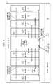
- the memory module 1 illustrated in FIG. 1has dimensions of 1.2 inches ⁇ 5.25 inches in accordance with the JEDEC standard. Eight DRAMs 2 as user data memories and one further DRAM 3 as error data memory are provided on at least one of the two placement surfaces of the memory module 1 .
- the memory module 1has an array of contact devices 10 as an electrical interface to a system board of a data memory system. From the array of contact devices 10 , an external data bus 51 and also an external control and address bus 63 are routed to a buffer/redriver module 4 .
- the buffer/redriver module 4is respectively connected to the DRAMS 2 , 3 via data signal lines 5 .
- An internal control and address busis routed in two branches 61 , 62 in each case between the buffer/redriver module 4 and the DRAMs 2 , 3 .
- FIG. 2indicates a second possibility for arranging the DRAMs 2 , 3 on the memory module 1 .
- the problem of an asymmetrical distribution of the capacitive loads on the internal control and address bus 61 , 62 and of a timing dependent on the furnishing of the DRAM 3 provided as an error data memoryremains in this case.
- the inventionis, therefore, based on the object of providing a memory module which enables the intergration of a buffer/redriver functionality and of an error data memory on the memory module.
- the intergrated buffer and error checking module of the present inventionis operable with different bus configurations of the memory module in the context of industry standards in force for the mechanical and electrical interface of the memory module. It is furthermore an object of the invention to provide a method for operating such a memory module.
- FIG. 1shows a schematic plan view of a first prior art memory module designed according to a buffer/redriver and error correction concept combined in a conventional manner
- FIG. 2shows a schematic plan view of a second prior art memory module designed according to a buffer/redriver and error correction concept combined in a conventional manner
- FIG. 3shows a schematic plan view of a memory module according to the invention in accordance with a first exemplary embodiment
- FIG. 4shows a schematic plan view of a third prior art memory module designed according to a buffer/redriver and error correction concept combined in a conventional manner
- FIG. 5shows a schematic plan view of a memory module according to the invention in accordance with a second exemplary embodiment
- Memory module 10Contact devices 2 Data memory device for user data 3 Data memory device for redundancy data 4, 4′ Buffer/redriver module 5 Data lines internal 51 Data lines external 61, 61′ Control and address lines internal 62, 62′ Control and address lines internal 63 Control and address lines external 7, 7′ Buffer and error checking module
- FIG. 3illustrates a memory module according to the invention.
- the routing of data signal lines 5 between the buffer and error checking module 7which, according to the invention, integrates a buffer/redriver functionality and an error data memory in a common device housing, and the remaining DRAMs 2 for storing the user data is significantly simplified just by the omission of connections to the DRAM 3 for error data storage of FIG. 1 or 2 .
- the same capacitive loadis present on each branch 61 , 62 of the internal control and address bus. In this case, the capacitive load is independent of whether an error correction is effected on the memory module.
- the memory module 1 according to the inventioncan also be operated with error correction with the same data transfer rate with regard to the user data as one of the memory modules in accordance with FIG. 1 and FIG. 2 without error correction.
- FIG. 4shows a conventional memory module 1 with two buffer/redriver modules 4 , 4 ′.
- a furnished DRAM 3 for error data storage purposesresults in an asymmetrical loading at least in one of the branches 61 , 61 ′, 62 , 62 ′ of the internal control and address bus system.
- the error data memoryis divided between two buffer and error checking modules 7 of the same type.
- the two buffer and error checking modules 7in each case furthermore contain a buffer/redriver functionality.
- the resultis a significantly simplified routing of the data signal lines 5 and also a symmetrical loading on all the branches 61 of the control and address bus.
- the division of the external data bus 51 , 51 ′ and of the external control and address bus 63 , 63 ′ into two branches in each caseresults, by comparison with the memory module from FIG. 3 , in a simplified routing with regard to the two external bus systems between the combined buffer and error checking modules 7 , 7 ′ and the array of contact devices 10 .
- the memory module according to the invention for incorporation into a data memory systemthus has at least one buffer and error checking module, which integrates in each case a buffer device and a data memory device for storing redundancy data within a common device housing.
- the integration of a buffer/redriver functionality and of an error data memory device within a common device housingis based on the consideration that, for DDRII and DDRIII concepts, the dimensions of a buffer/redriver module embodied using customary semiconductor technology is determined essentially by the number of connections of the buffer/redriver module, but not by the buffer/redriver functionality realized in a semiconductor substrate of the buffer/redriver module. In this case, only a small part of the semiconductor substrate of the buffer/redriver modules is utilized by the buffer/redriver functionality.
- the disparity between the space requirement for realizing the buffer functionality and the space requirement for embodying the connectionsresults from a buffer functionality that can be realized relatively simply in the semiconductor substrate, on the one hand, and a high number of electrical connections, in particular of data line connections, on the other hand.
- said buffer/redriver modulegenerally by itself has to be provided with 256 connections for transferring data signals.
- the number of 256 connectionsresults here from in each case 64 connections for the data bus systems of the system board and of the memory module, and also from the fact that a shielding line generally has to be assigned to each data signal line at data transfer rates of more than 500 MHz/s/pin.
- the number of connectionsincreases in accordance with the width of a redundancy data bus system.
- the memory module according to the inventionwith a combined buffer and error checking module, bus lines between an error data memory device and a buffer/redriver module are obviated.
- the combined buffer and error checking moduleadvantageously tends rather to have fewer connections than a comparable conventional buffer/redriver module.
- the functionality of the error data memorycan be embodied in the context of conventional technologies, for instance as embedded DRAM, in substantial parts within the otherwise unutilized region of the semiconductor substrate of a buffer/redriver module.
- the integration of the error data memory device and of the buffer/redriver functionality within a combined buffer and error checking modulethus advantageously reduces the space requirement for a combined buffer/redriver and error correction concept.
- the space requirement for an integrated buffer and error checking moduletends to be smaller than the accumulated space requirement of a customary buffer/redriver module and an error data memory device.
- the total space saved according to the invention on the memory moduleenables the arrangement (placement) and the connection (routing) of the required number of data memory devices on the memory module and a simultaneous realization of an error correction concept and a buffer/redriver concept in the context of the memory module dimensions prescribed by industry standards.
- Memory modules with larger dimensionsare advantageously unnecessary with the memory module according to the invention.
- the memory module according to the inventionhas a higher signal integrity due to shorter line paths. Costs incurred by virtue of a larger area of the memory modules, by virtue of the need for new production apparatuses and, in particular, also by virtue of a changeover of the production or memory modules and data memory systems to a new module size are avoided according to the invention. A new industry standard is unnecessary and a cost-intensive splitting up of production lines is avoided.
- the layouts of the signal lines for corresponding types of memory modules with and without error correctiondo not differ, or differ only to an insignificant extent.
- the two corresponding types of memory modules with and without error correctionmerely differ either in the design of the buffer and error checking modules furnished or in the design of one or a small number of signal lines controlling the functionality of the buffer and error checking module. Consequently, each of the buffer and error checking modules, independently of the type of memory module, is always connected to an even number of data memory devices for storing the user data. Symmetrical topologies for the embodiment of the signal lines can thus be found for corresponding types of memory modules with and without error correction. Symmetrical loads in particular on the control and address lines advantageously result.
- the timing in particular of the control and address signalsis consequently determined unambiguously for corresponding types of memory modules with and without error correction.
- Waiting cycles (latencies) between the transfer of control and address signals on the control and address signal lines, on the one hand, and the transfer of data on data signal lines, on the other hand, as are known for instance from DDRI concepts in the operation of memory modules with error correction,are unnecessary.
- the control and address signalsare first of all transferred to a buffer memory and are only transferred to the data memory devices in a subsequent cycle together with the data signals output in a manner delayed by one cycle.
- the waiting cyclesignificantly reduces the data transfer rate in the data memory system particularly in the case of non-ordered address accesses (random access).
- the performance of the memory moduleis increased according to the invention.
- the required size of the error data memorydepends only on the memory capacity of the memory module. Therefore, the embodiment of the buffer and error checking module is advantageously largely independent of the data bus width of the data memory devices arranged on the respective memory module.
- the combined buffer and error checking moduleis furthermore adapted to the requirements of the memory checking module of the data memory system, the requirement made of the error data memory realized in the buffer and error checking module can advantageously be reduced for instance with regard to the access times compared with the user data memory.
- the error data memorycan thus be designed for example using the embedded technology corresponding to the respective data memory device.
- the buffer and error checking modulepreferably comprises not only the error data memory but also an error detection and an error correction unit.
- the redundancy data(error data, ECC information items) are evaluated in a memory checking module assigned to the memory system. If a data error occurs, then the data error is registered, and if appropriate corrected, in the memory control device.
- possibly erroneous dataare already detected on the memory module and corrected case by case. Since significantly fewer erroneous data are consequently transferred between the memory checking module and the memory modules, the data transfer rate of the data memory system is increased further with regard to the user data.
- the error correction on the memory module and an additional independent error correction in the memory checking moduleenable an error analysis of the entire data memory system. This enables an optimization of the bus system between the memory checking module and the memory modules. If the bus system is optimized sufficiently by means of the error analysis, then there is no need for a bus system assigned to the redundancy data between the memory checking module, on the one hand, and the memory modules, on the other hand.
- said memory moduleadvantageously has no connections for redundancy data lines. The routing of the conductor tracks on a system board of the data memory system, which system board can be populated with the memory modules, is then simplified due to the smaller number of conductor tracks.
- a simple conversion of a data memory system without error correction into a data memory system with error correctionthen also results in a particularly advantageous manner.
- the conversionis effected without further measures on the further system components of the data memory system solely through the replacement of memory modules without error correction by memory modules with error correction.
- the system boardcorresponds in terms of its design to a system board without error correction devices.
- the memory modulehas a possibility for signaling a data error.
- a memory module or a data memory device with accumulated error resultscan advantageously be identified through an evaluation of the data error in a higher processing plane of the data memory system. Repeatedly defective data memory areas can thus be masked out. The accompanying minimization of the number of error results further increases the performance of the data memory system.
- the identification and masking-out of defective memory cells on the memory moduleis preferably effected in the buffer and error checking module, which then has an error evaluation unit suitable therefor.
- Data memory devicesare usually designed as DRAM modules.
- Data transfer rates for which the advantages of the memory module according to the invention are manifestedgenerally presuppose DRAMs with a DDR interface.
- the buffer and error checking module according to the invention for memory modules operated in data memory systemshas, besides the required connection devices and a buffer/redriver functionality which is formed in a semiconductor substrate and is suitable for conditioning at least data signals that are transferred to and from the memory module, a memory cell array which is formed in the semiconductor substrate and is operated as an error data memory for memory modules.
- the buffer and error checking modulehas an error detection unit.
- the error detection unitUpon reception of user data from the data memory system, the error detection unit forms a set of redundancy data assigned to the received user data, which set of redundancy data is stored in the memory cell array of the buffer and error checking module.
- a corresponding set of check datais formed in the error detection unit and compared with the assigned redundancy data.
- the error detection unitregisters erroneous user data from the comparison of the stored redundancy data with the corresponding check data.
- the buffer and error checking module according to the inventionis preferably provided with an error correction unit, which is suitable for correcting the erroneous user data according to known algorithms on the basis of the stored redundancy data and the corresponding check data.
- the buffer and error checking modulehas an error signaling unit.
- Information on the occurrence and on the type of data errorsfor instance correctable single-bit errors or uncorrectable double-bit errors, can then be transferred to a further component of the data memory system for error analysis purposes.
- the buffer and error checking moduleaccording to the invention with an error evaluation unit.
- the error evaluation unitis suitable for analyzing the data errors that occur on the memory module and for masking out memory cells or memory areas identified as repeatedly defective. The transfer of erroneous user data is thus restricted in a particularly advantageous manner. A data transfer rate of the data memory system referring to the error-free transfer of user data is thus increased further.
- the method according to the inventiondescribes the operation of a memory module according to the invention having a plurality of data memory devices for storing user data and a buffer and error checking module in a data memory system.
- user data from a memory control device of the data memory systemare received and conditioned by means of the buffer and error checking module on the memory module. Consequently, in the buffer and error checking module, a corresponding set of redundancy data is formed with respect to the user data.
- the user dataare stored in the data memory devices and the corresponding set of redundancy data is stored in the buffer and error checking module.
- a corresponding set of check datais formed in the buffer and error checking module.
- An error detection and an error correction of data errors that have occurred on the memory modulesare thus effected, according to the invention, in the memory modules themselves. Since error events on memory modules generally involve so-called soft errors in DRAM memory cells, or the failure of entire modules, it is possible, first of all, for unnecessary lines or connections for the redundant data bus to be avoided in an advantageous manner on the system board. On the other hand, the performance of the system is also increased since no erroneous data are transferred between the memory modules and the memory checking module. If the system board of a data memory system previously had to be provided with an extended data bus width and be respectively adapted to an error correction concept, the method according to the invention enables simple upgrading of a data memory system just by exchanging memory modules.
- the occurrence of an error eventis transferred to at least one further component of the memory system, where a further evaluation of error events is possible.
- a further evaluation of error eventsis possible.
- data memory devices or memory modules with a high number of error eventsare identified.
- the relevant memory areamay either be masked out or be provided for exchange.
- Memory modules operated according to the inventioncan be used to optimize data memory systems.
- a redundancy bus system for transferring further redundancy datais provided in precursor systems between the memory checking device and the memory modules. Consequently, an error correction as already described is carried out internally on the memory module.
- the consistency of the user data transferred between the memory modules and the memory checking deviceis checked on the basis of the further redundancy data transferred on the redundancy bus system. It can thus be identified for each error event whether an error source is to be assigned to the memory module or to the bus system of the data memory system. Consequently, the bus system of the data memory system is reworked until only a tolerable number of errors is to be assigned to the bus system.
- the specificationmay have presented the method and/or process of the present invention as a particular sequence of steps. However, to the extent that the method or process does not rely on the particular order of steps set forth herein, the method or process should not be limited to the particular sequence of steps described. As one of ordinary skill in the art would appreciate, other sequences of steps may be possible. Therefore, the particular order of the steps set forth in the specification should not be construed as limitations on the claims. In addition, the claims directed to the method and/or process of the present invention should not be limited to the performance of their steps in the order written, and one skilled in the art can readily appreciate that the sequences may be varied and still remain within the spirit and scope of the present invention.
Landscapes
- Techniques For Improving Reliability Of Storages (AREA)
- For Increasing The Reliability Of Semiconductor Memories (AREA)
- Debugging And Monitoring (AREA)
Abstract
Description
| 1 | |||
| 10 | |||
| 2 | Data memory device for | ||
| 3 | Data memory device for | ||
| 4, 4′ | Buffer/ | ||
| 5 | Data lines internal | ||
| 51 | Data lines external | ||
| 61, 61′ | Control and address lines internal | ||
| 62, 62′ | Control and address lines internal | ||
| 63 | Control and address lines external | ||
| 7, 7′ | Buffer and error checking module | ||
Claims (18)
Applications Claiming Priority (2)
| Application Number | Priority Date | Filing Date | Title |
|---|---|---|---|
| DE10255872.8 | 2002-11-29 | ||
| DE10255872ADE10255872B4 (en) | 2002-11-29 | 2002-11-29 | Memory module and method for operating a memory module in a data storage system |
Publications (2)
| Publication Number | Publication Date |
|---|---|
| US20040151038A1 US20040151038A1 (en) | 2004-08-05 |
| US7275189B2true US7275189B2 (en) | 2007-09-25 |
Family
ID=32335851
Family Applications (1)
| Application Number | Title | Priority Date | Filing Date |
|---|---|---|---|
| US10/724,135Expired - Fee RelatedUS7275189B2 (en) | 2002-11-29 | 2003-12-01 | Memory module and method for operating a memory module in a data memory system |
Country Status (3)
| Country | Link |
|---|---|
| US (1) | US7275189B2 (en) |
| CN (1) | CN1266611C (en) |
| DE (1) | DE10255872B4 (en) |
Cited By (9)
| Publication number | Priority date | Publication date | Assignee | Title |
|---|---|---|---|---|
| US20050010737A1 (en)* | 2000-01-05 | 2005-01-13 | Fred Ware | Configurable width buffered module having splitter elements |
| US20060236201A1 (en)* | 2003-04-14 | 2006-10-19 | Gower Kevin C | High reliability memory module with a fault tolerant address and command bus |
| US20070070669A1 (en)* | 2005-09-26 | 2007-03-29 | Rambus Inc. | Memory module including a plurality of integrated circuit memory devices and a plurality of buffer devices in a matrix topology |
| US20080046802A1 (en)* | 2006-08-18 | 2008-02-21 | Fujitsu Limited | Memory controller and method of controlling memory |
| US20080266778A1 (en)* | 2004-12-23 | 2008-10-30 | Intel Corporation | Memory module routing |
| US7562271B2 (en) | 2005-09-26 | 2009-07-14 | Rambus Inc. | Memory system topologies including a buffer device and an integrated circuit memory device |
| US20100037122A1 (en)* | 2008-08-07 | 2010-02-11 | International Business Machines Corporation | Memory Controller for Reducing Time to Initialize Main Memory |
| WO2013115783A1 (en)* | 2012-01-31 | 2013-08-08 | Hewlett-Packard Development Company, L.P. | Memory module buffer data storage |
| US11328764B2 (en) | 2005-09-26 | 2022-05-10 | Rambus Inc. | Memory system topologies including a memory die stack |
Families Citing this family (42)
| Publication number | Priority date | Publication date | Assignee | Title |
|---|---|---|---|---|
| KR100585158B1 (en)* | 2004-09-13 | 2006-05-30 | 삼성전자주식회사 | ECC memory module |
| DE102004056214B4 (en)* | 2004-11-22 | 2006-12-14 | Infineon Technologies Ag | memory buffer |
| US8359187B2 (en) | 2005-06-24 | 2013-01-22 | Google Inc. | Simulating a different number of memory circuit devices |
| US9507739B2 (en) | 2005-06-24 | 2016-11-29 | Google Inc. | Configurable memory circuit system and method |
| US8041881B2 (en) | 2006-07-31 | 2011-10-18 | Google Inc. | Memory device with emulated characteristics |
| US8060774B2 (en) | 2005-06-24 | 2011-11-15 | Google Inc. | Memory systems and memory modules |
| US7590796B2 (en) | 2006-07-31 | 2009-09-15 | Metaram, Inc. | System and method for power management in memory systems |
| US8081474B1 (en) | 2007-12-18 | 2011-12-20 | Google Inc. | Embossed heat spreader |
| US8438328B2 (en) | 2008-02-21 | 2013-05-07 | Google Inc. | Emulation of abstracted DIMMs using abstracted DRAMs |
| US7609567B2 (en) | 2005-06-24 | 2009-10-27 | Metaram, Inc. | System and method for simulating an aspect of a memory circuit |
| US8055833B2 (en) | 2006-10-05 | 2011-11-08 | Google Inc. | System and method for increasing capacity, performance, and flexibility of flash storage |
| US8386722B1 (en) | 2008-06-23 | 2013-02-26 | Google Inc. | Stacked DIMM memory interface |
| US7386656B2 (en) | 2006-07-31 | 2008-06-10 | Metaram, Inc. | Interface circuit system and method for performing power management operations in conjunction with only a portion of a memory circuit |
| US9171585B2 (en) | 2005-06-24 | 2015-10-27 | Google Inc. | Configurable memory circuit system and method |
| US8130560B1 (en) | 2006-11-13 | 2012-03-06 | Google Inc. | Multi-rank partial width memory modules |
| US10013371B2 (en) | 2005-06-24 | 2018-07-03 | Google Llc | Configurable memory circuit system and method |
| US8111566B1 (en) | 2007-11-16 | 2012-02-07 | Google, Inc. | Optimal channel design for memory devices for providing a high-speed memory interface |
| US8796830B1 (en) | 2006-09-01 | 2014-08-05 | Google Inc. | Stackable low-profile lead frame package |
| US7472220B2 (en) | 2006-07-31 | 2008-12-30 | Metaram, Inc. | Interface circuit system and method for performing power management operations utilizing power management signals |
| US8090897B2 (en) | 2006-07-31 | 2012-01-03 | Google Inc. | System and method for simulating an aspect of a memory circuit |
| US8077535B2 (en) | 2006-07-31 | 2011-12-13 | Google Inc. | Memory refresh apparatus and method |
| US8089795B2 (en) | 2006-02-09 | 2012-01-03 | Google Inc. | Memory module with memory stack and interface with enhanced capabilities |
| US7392338B2 (en) | 2006-07-31 | 2008-06-24 | Metaram, Inc. | Interface circuit system and method for autonomously performing power management operations in conjunction with a plurality of memory circuits |
| US20080028136A1 (en) | 2006-07-31 | 2008-01-31 | Schakel Keith R | Method and apparatus for refresh management of memory modules |
| US20080082763A1 (en) | 2006-10-02 | 2008-04-03 | Metaram, Inc. | Apparatus and method for power management of memory circuits by a system or component thereof |
| US7580312B2 (en) | 2006-07-31 | 2009-08-25 | Metaram, Inc. | Power saving system and method for use with a plurality of memory circuits |
| US8327104B2 (en) | 2006-07-31 | 2012-12-04 | Google Inc. | Adjusting the timing of signals associated with a memory system |
| US8244971B2 (en) | 2006-07-31 | 2012-08-14 | Google Inc. | Memory circuit system and method |
| KR101377305B1 (en) | 2005-06-24 | 2014-03-25 | 구글 인코포레이티드 | An integrated memory core and memory interface circuit |
| US8335894B1 (en) | 2008-07-25 | 2012-12-18 | Google Inc. | Configurable memory system with interface circuit |
| US9542352B2 (en) | 2006-02-09 | 2017-01-10 | Google Inc. | System and method for reducing command scheduling constraints of memory circuits |
| US8397013B1 (en) | 2006-10-05 | 2013-03-12 | Google Inc. | Hybrid memory module |
| US7414917B2 (en)* | 2005-07-29 | 2008-08-19 | Infineon Technologies | Re-driving CAwD and rD signal lines |
| WO2007028109A2 (en) | 2005-09-02 | 2007-03-08 | Metaram, Inc. | Methods and apparatus of stacking drams |
| US9632929B2 (en) | 2006-02-09 | 2017-04-25 | Google Inc. | Translating an address associated with a command communicated between a system and memory circuits |
| US7724589B2 (en) | 2006-07-31 | 2010-05-25 | Google Inc. | System and method for delaying a signal communicated from a system to at least one of a plurality of memory circuits |
| US8209479B2 (en) | 2007-07-18 | 2012-06-26 | Google Inc. | Memory circuit system and method |
| US8080874B1 (en) | 2007-09-14 | 2011-12-20 | Google Inc. | Providing additional space between an integrated circuit and a circuit board for positioning a component therebetween |
| DE202010017690U1 (en) | 2009-06-09 | 2012-05-29 | Google, Inc. | Programming dimming terminating resistor values |
| US8782477B2 (en)* | 2011-05-11 | 2014-07-15 | Jabil Circuit, Inc. | High-speed serial interface bridge adapter for signal integrity verification |
| JP6006920B2 (en)* | 2011-07-04 | 2016-10-12 | ピーエスフォー ルクスコ エスエイアールエルPS4 Luxco S.a.r.l. | Semiconductor module and module substrate |
| KR102827608B1 (en)* | 2016-12-14 | 2025-07-03 | 에스케이하이닉스 주식회사 | Memory system and error correcting method of the same |
Citations (6)
| Publication number | Priority date | Publication date | Assignee | Title |
|---|---|---|---|---|
| US5541941A (en) | 1994-01-28 | 1996-07-30 | International Business Machines Corporation | Method and structure for providing automatic parity sensing |
| US6092146A (en)* | 1997-07-31 | 2000-07-18 | Ibm | Dynamically configurable memory adapter using electronic presence detects |
| US6185718B1 (en)* | 1998-02-27 | 2001-02-06 | International Business Machines Corporation | Memory card design with parity and ECC for non-parity and non-ECC systems |
| US6421274B1 (en)* | 2001-03-23 | 2002-07-16 | Mitsubishi Denki Kabushiki Kaisha | Semiconductor memory device and reading and writing method thereof |
| US6791877B2 (en)* | 2001-06-11 | 2004-09-14 | Renesas Technology Corporation | Semiconductor device with non-volatile memory and random access memory |
| US6832340B2 (en)* | 2000-01-26 | 2004-12-14 | Hewlett-Packard Development Company, L.P. | Real-time hardware memory scrubbing |
- 2002
- 2002-11-29DEDE10255872Apatent/DE10255872B4/ennot_activeExpired - Fee Related
- 2003
- 2003-12-01CNCNB200310119509XApatent/CN1266611C/ennot_activeExpired - Fee Related
- 2003-12-01USUS10/724,135patent/US7275189B2/ennot_activeExpired - Fee Related
Patent Citations (6)
| Publication number | Priority date | Publication date | Assignee | Title |
|---|---|---|---|---|
| US5541941A (en) | 1994-01-28 | 1996-07-30 | International Business Machines Corporation | Method and structure for providing automatic parity sensing |
| US6092146A (en)* | 1997-07-31 | 2000-07-18 | Ibm | Dynamically configurable memory adapter using electronic presence detects |
| US6185718B1 (en)* | 1998-02-27 | 2001-02-06 | International Business Machines Corporation | Memory card design with parity and ECC for non-parity and non-ECC systems |
| US6832340B2 (en)* | 2000-01-26 | 2004-12-14 | Hewlett-Packard Development Company, L.P. | Real-time hardware memory scrubbing |
| US6421274B1 (en)* | 2001-03-23 | 2002-07-16 | Mitsubishi Denki Kabushiki Kaisha | Semiconductor memory device and reading and writing method thereof |
| US6791877B2 (en)* | 2001-06-11 | 2004-09-14 | Renesas Technology Corporation | Semiconductor device with non-volatile memory and random access memory |
Non-Patent Citations (2)
| Title |
|---|
| "A Highly Efficient Transparent Online Memory Test" by Thaller in the International Test Conference, 2001 Proceedings Publication Date: 2001 pp. 230-239.* |
| "Achieving Fault Secureness in Parity Prediction Arithmetic Operators: General Conditions and Implementations" by Nicolaidis et al. in: European Design and Test Conference, 1996. ED&TC 96. Proceedings Publication Date: Mar. 11-14, 1996 pp. 186-193.* |
Cited By (28)
| Publication number | Priority date | Publication date | Assignee | Title |
|---|---|---|---|---|
| US20050010737A1 (en)* | 2000-01-05 | 2005-01-13 | Fred Ware | Configurable width buffered module having splitter elements |
| US7380179B2 (en)* | 2003-04-14 | 2008-05-27 | International Business Machines Corporation | High reliability memory module with a fault tolerant address and command bus |
| US20060236201A1 (en)* | 2003-04-14 | 2006-10-19 | Gower Kevin C | High reliability memory module with a fault tolerant address and command bus |
| US20080266778A1 (en)* | 2004-12-23 | 2008-10-30 | Intel Corporation | Memory module routing |
| US8539152B2 (en) | 2005-09-26 | 2013-09-17 | Rambus Inc. | Memory system topologies including a buffer device and an integrated circuit memory device |
| US9865329B2 (en) | 2005-09-26 | 2018-01-09 | Rambus Inc. | Memory system topologies including a buffer device and an integrated circuit memory device |
| US7464225B2 (en) | 2005-09-26 | 2008-12-09 | Rambus Inc. | Memory module including a plurality of integrated circuit memory devices and a plurality of buffer devices in a matrix topology |
| US7562271B2 (en) | 2005-09-26 | 2009-07-14 | Rambus Inc. | Memory system topologies including a buffer device and an integrated circuit memory device |
| US12394471B2 (en) | 2005-09-26 | 2025-08-19 | Rambus Inc. | Memory system topologies including a memory die stack |
| US7685364B2 (en) | 2005-09-26 | 2010-03-23 | Rambus Inc. | Memory system topologies including a buffer device and an integrated circuit memory device |
| US7729151B2 (en) | 2005-09-26 | 2010-06-01 | Rambus Inc. | System including a buffered memory module |
| US8108607B2 (en) | 2005-09-26 | 2012-01-31 | Rambus Inc. | Memory system topologies including a buffer device and an integrated circuit memory device |
| US11727982B2 (en) | 2005-09-26 | 2023-08-15 | Rambus Inc. | Memory system topologies including a memory die stack |
| US11328764B2 (en) | 2005-09-26 | 2022-05-10 | Rambus Inc. | Memory system topologies including a memory die stack |
| US20070070669A1 (en)* | 2005-09-26 | 2007-03-29 | Rambus Inc. | Memory module including a plurality of integrated circuit memory devices and a plurality of buffer devices in a matrix topology |
| US11043258B2 (en) | 2005-09-26 | 2021-06-22 | Rambus Inc. | Memory system topologies including a memory die stack |
| US10672458B1 (en) | 2005-09-26 | 2020-06-02 | Rambus Inc. | Memory system topologies including a buffer device and an integrated circuit memory device |
| US9117035B2 (en) | 2005-09-26 | 2015-08-25 | Rambus Inc. | Memory system topologies including a buffer device and an integrated circuit memory device |
| US10535398B2 (en) | 2005-09-26 | 2020-01-14 | Rambus Inc. | Memory system topologies including a buffer device and an integrated circuit memory device |
| US9563583B2 (en) | 2005-09-26 | 2017-02-07 | Rambus Inc. | Memory system topologies including a buffer device and an integrated circuit memory device |
| US10381067B2 (en) | 2005-09-26 | 2019-08-13 | Rambus Inc. | Memory system topologies including a buffer device and an integrated circuit memory device |
| US20080046802A1 (en)* | 2006-08-18 | 2008-02-21 | Fujitsu Limited | Memory controller and method of controlling memory |
| US8667372B2 (en)* | 2006-08-18 | 2014-03-04 | Fujitsu Limited | Memory controller and method of controlling memory |
| US8205138B2 (en)* | 2008-08-07 | 2012-06-19 | International Business Machines Corporation | Memory controller for reducing time to initialize main memory |
| US20100037122A1 (en)* | 2008-08-07 | 2010-02-11 | International Business Machines Corporation | Memory Controller for Reducing Time to Initialize Main Memory |
| GB2512786B (en)* | 2012-01-31 | 2016-07-06 | Hewlett Packard Development Co Lp | Memory module buffer data storage |
| GB2512786A (en)* | 2012-01-31 | 2014-10-08 | Hewlett Packard Development Co | Memory module buffer data storage |
| WO2013115783A1 (en)* | 2012-01-31 | 2013-08-08 | Hewlett-Packard Development Company, L.P. | Memory module buffer data storage |
Also Published As
| Publication number | Publication date |
|---|---|
| CN1504897A (en) | 2004-06-16 |
| CN1266611C (en) | 2006-07-26 |
| DE10255872B4 (en) | 2004-09-30 |
| DE10255872A1 (en) | 2004-06-24 |
| US20040151038A1 (en) | 2004-08-05 |
Similar Documents
| Publication | Publication Date | Title |
|---|---|---|
| US7275189B2 (en) | Memory module and method for operating a memory module in a data memory system | |
| US20220138042A1 (en) | Memory Error Detection | |
| EP2035938B1 (en) | Improving reliability, availability, and serviceability in a memory device | |
| US5923682A (en) | Error correction chip for memory applications | |
| US9431063B2 (en) | Stacked memory having same timing domain read data and redundancy | |
| US8255783B2 (en) | Apparatus, system and method for providing error protection for data-masking bits | |
| US7984329B2 (en) | System and method for providing DRAM device-level repair via address remappings external to the device | |
| US20180143873A1 (en) | Memory repair method and apparatus based on error code tracking | |
| US20050041504A1 (en) | Method of operating a memory system including an integrated circuit buffer device | |
| US20020163784A1 (en) | Memory module having balanced data i/o contacts pads | |
| US7697332B2 (en) | Placement and routing of ECC memory devices for improved signal timing | |
| US20040237001A1 (en) | Memory integrated circuit including an error detection mechanism for detecting errors in address and control signals | |
| US7483321B2 (en) | Semiconductor memory device capable of checking a redundancy code and memory system and computer system having the same | |
| KR100609343B1 (en) | System and method for multi-bit error protection in computer memory systems | |
| US7375971B2 (en) | Memory module with an electronic printed circuit board and a plurality of semiconductor chips of the same type | |
| US20040085795A1 (en) | Memory module and memory configuration with stub-free signal lines and distributed capacitive loads | |
| US7633767B2 (en) | Memory modules including SIMM and DIMM-type connection structures and related memory systems | |
| US5936844A (en) | Memory system printed circuit board | |
| US20060095826A1 (en) | Semiconductor memory chip, semiconductor memory module and method for transmitting write data to semiconductor memory chips | |
| JP2000066962A (en) | Storage device | |
| US7106613B2 (en) | Memory module and a method of arranging a signal line of the same | |
| CN111736760B (en) | Dynamic random storage method and system | |
| US20240272982A1 (en) | Quad-channel memory module reliability | |
| EP4630926A1 (en) | In-package error correction for multi-die memory stacks | |
| JP2006004133A (en) | Error correction and detection device in information processing device |
Legal Events
| Date | Code | Title | Description |
|---|---|---|---|
| AS | Assignment | Owner name:INFINEON TECHNOLOGIES AG, GERMANY Free format text:ASSIGNMENT OF ASSIGNORS INTEREST;ASSIGNORS:RUCKERBAUER, HERMANN;BRAUN, GEORG;REEL/FRAME:015710/0375;SIGNING DATES FROM 20050130 TO 20050204 | |
| STCF | Information on status: patent grant | Free format text:PATENTED CASE | |
| CC | Certificate of correction | ||
| FEPP | Fee payment procedure | Free format text:PAYOR NUMBER ASSIGNED (ORIGINAL EVENT CODE: ASPN); ENTITY STATUS OF PATENT OWNER: LARGE ENTITY | |
| AS | Assignment | Owner name:QIMONDA AG, GERMANY Free format text:ASSIGNMENT OF ASSIGNORS INTEREST;ASSIGNOR:INFINEON TECHNOLOGIES AG;REEL/FRAME:023796/0001 Effective date:20060425 | |
| FPAY | Fee payment | Year of fee payment:4 | |
| FPAY | Fee payment | Year of fee payment:8 | |
| AS | Assignment | Owner name:INFINEON TECHNOLOGIES AG, GERMANY Free format text:ASSIGNMENT OF ASSIGNORS INTEREST;ASSIGNOR:QIMONDA AG;REEL/FRAME:035623/0001 Effective date:20141009 | |
| AS | Assignment | Owner name:POLARIS INNOVATIONS LIMITED, IRELAND Free format text:ASSIGNMENT OF ASSIGNORS INTEREST;ASSIGNOR:INFINEON TECHNOLOGIES AG;REEL/FRAME:036873/0758 Effective date:20150708 | |
| FEPP | Fee payment procedure | Free format text:MAINTENANCE FEE REMINDER MAILED (ORIGINAL EVENT CODE: REM.); ENTITY STATUS OF PATENT OWNER: LARGE ENTITY | |
| LAPS | Lapse for failure to pay maintenance fees | Free format text:PATENT EXPIRED FOR FAILURE TO PAY MAINTENANCE FEES (ORIGINAL EVENT CODE: EXP.); ENTITY STATUS OF PATENT OWNER: LARGE ENTITY | |
| STCH | Information on status: patent discontinuation | Free format text:PATENT EXPIRED DUE TO NONPAYMENT OF MAINTENANCE FEES UNDER 37 CFR 1.362 | |
| FP | Lapsed due to failure to pay maintenance fee | Effective date:20190925 |