US7274094B2 - Leadless packaging for image sensor devices - Google Patents
Leadless packaging for image sensor devicesDownload PDFInfo
- Publication number
- US7274094B2 US7274094B2US10/233,319US23331902AUS7274094B2US 7274094 B2US7274094 B2US 7274094B2US 23331902 AUS23331902 AUS 23331902AUS 7274094 B2US7274094 B2US 7274094B2
- Authority
- US
- United States
- Prior art keywords
- package
- aperture
- top surface
- side cavity
- package shell
- Prior art date
- Legal status (The legal status is an assumption and is not a legal conclusion. Google has not performed a legal analysis and makes no representation as to the accuracy of the status listed.)
- Expired - Lifetime, expires
Links
Images


Classifications
- H—ELECTRICITY
- H10—SEMICONDUCTOR DEVICES; ELECTRIC SOLID-STATE DEVICES NOT OTHERWISE PROVIDED FOR
- H10F—INORGANIC SEMICONDUCTOR DEVICES SENSITIVE TO INFRARED RADIATION, LIGHT, ELECTROMAGNETIC RADIATION OF SHORTER WAVELENGTH OR CORPUSCULAR RADIATION
- H10F77/00—Constructional details of devices covered by this subclass
- H10F77/50—Encapsulations or containers
- H—ELECTRICITY
- H01—ELECTRIC ELEMENTS
- H01L—SEMICONDUCTOR DEVICES NOT COVERED BY CLASS H10
- H01L2224/00—Indexing scheme for arrangements for connecting or disconnecting semiconductor or solid-state bodies and methods related thereto as covered by H01L24/00
- H01L2224/01—Means for bonding being attached to, or being formed on, the surface to be connected, e.g. chip-to-package, die-attach, "first-level" interconnects; Manufacturing methods related thereto
- H01L2224/10—Bump connectors; Manufacturing methods related thereto
- H01L2224/15—Structure, shape, material or disposition of the bump connectors after the connecting process
- H01L2224/16—Structure, shape, material or disposition of the bump connectors after the connecting process of an individual bump connector
- H01L2224/161—Disposition
- H01L2224/16151—Disposition the bump connector connecting between a semiconductor or solid-state body and an item not being a semiconductor or solid-state body, e.g. chip-to-substrate, chip-to-passive
- H01L2224/16221—Disposition the bump connector connecting between a semiconductor or solid-state body and an item not being a semiconductor or solid-state body, e.g. chip-to-substrate, chip-to-passive the body and the item being stacked
- H01L2224/16245—Disposition the bump connector connecting between a semiconductor or solid-state body and an item not being a semiconductor or solid-state body, e.g. chip-to-substrate, chip-to-passive the body and the item being stacked the item being metallic
Definitions
- the present inventionrelates to packaging of optically interactive microelectronic devices. More particularly, the present invention relates to a leadless package for a solid-state image sensor and methods for its assembly.
- Optically interactive microelectronic devicesfor example, charge-coupled device (CCD) image sensors or complementary metal-oxide semiconductor (CMOS) image sensors, require packaging that provides protection from environmental conditions while allowing light or other forms of radiation to pass through to a surface where sensing circuitry is located. Typically, this has been accomplished by placing a sensor device in the form of a semiconductor die into a cavity of a plastic or ceramic housing, wire bonding electrical connection points on the semiconductor die to conductive elements associated with the housing and placing a window or transparent lid over the cavity.
- This packaging arrangementcan require several fabrication steps and raises concerns of durability and size.
- Wire bondsfor instance, involve special considerations during package formation due to the fragile nature of the thin wires and bond connections, and also call for increased package size in order to accommodate the arched wire bonds within the package cavity. Further, the housing construction for such a package requires a large volume of material held within tight tolerances, increasing cost and production time. The completed sensor package is large and takes up valuable space in high-density circuit assemblies.
- U.S. Pat. No. 6,351,027 to Giboney et al.discloses a chip-mounted enclosure wherein a sidewall piece is mounted directly to a semiconductor die to surround sensing or light-emitting circuitry and a transparent cover is attached over the sidewall piece.
- U.S. Pat. No. 6,147,389 to Stern et al.discloses an image sensor package with a stand-off frame for a window and reference plane members for simple and accurate mounting of an image sensor within the package. While these and other designs offer some packaging improvements, they still raise issues regarding numerous housing elements requiring multiple steps of assembly and difficulties with hermetically sealing the packages. Further, the incorporation of these structures into larger circuit assemblies often involves the use of delicate leads or solder pad arrangements which are not suitable for today's high-speed automated assembly techniques.
- the present inventionprovides a method and apparatus for packaging an optically interactive microelectronic device such as an image sensor within a leadless shell having a bottom-side cavity.
- the image sensorin the form of a semiconductor die or chip, is mounted to conductive elements within the cavity in a flip-chip configuration such that the active die surface containing sensing circuitry is exposed through an aperture in the top surface of the shell.
- a transparent lidis placed over the aperture to protect the active surface from environmental conditions and may also provide an optical function such as, for example, focusing or filtering light passing therethrough.
- a plurality of castellated solder pads in electrical communication with the conductive elementsis formed around the periphery of the shell and extends to the bottom side of the shell for attachment of the image sensor package to a carrier substrate such as a printed circuit board (PCB) or other higher-level packaging.
- a carrier substratesuch as a printed circuit board (PCB) or other higher-level packaging.
- optically interactiveas used herein is meant to encompass devices sensitive to various wavelengths of light or other forms of radiation, such as, but not limited to, CCD and CMOS image sensors, EPROMs, and photodiodes, as well as light-emitting devices including semiconductor lasers and light-emitting diodes.
- an image sensor chipis flip-chip mounted to the shell with gold—gold interconnect bonding and the active surface of the chip is buried in a transparent encapsulant which serves to bond the chip onto the package casing, maintain bond integrity and protect the chip edges.
- the encapsulantis subsequently capped with a transparent lid held in place by adhesion to the encapsulant material.
- the back of the image sensor chipis left exposed within the bottom-side cavity of the shell.
- the shellis prefabricated with a transparent lid mounted over the aperture of the shell.
- Gold-gold interconnect bondingis still used to mount the image sensor package in a flip-chip fashion, but the use of adhesive and encapsulant material is kept to a minimum.
- a backing capis placed over the back of the image sensor chip within the bottom-side cavity to hermetically seal the package and protect the image sensor chip.
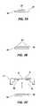
- FIG. 1is a perspective top view of an image sensor package according to the present invention showing a transparent window mounted on the top surface of a package shell and the active surface of an image sensor chip exposed therethrough.
- FIG. 2is a perspective bottom view of the image sensor package of FIG. 1 showing a bottom-side cavity formed in the bottom surface of the package shell and containing the image sensor package.
- FIG. 3is a partial side view of an image sensor package according to the present invention mounted to a carrier substrate.
- FIG. 4is a sectional side view of a first embodiment of an image sensor package according to the present invention wherein a transparent window is mounted in an encapsulant covering the active surface of an image sensor chip.
- FIGS. 5A through 5Hare views showing a method of assembly for the first embodiment of an image sensor package depicted in FIG. 4 .
- FIG. 6is a sectional side view of a second embodiment of an image sensor package according to the present invention wherein a package shell is prefabricated with a transparent lid and a backing cap is placed over a back-side cavity to hermetically seal the image sensor package.
- FIGS. 7A through 7Hare views showing a method of assembly for the second embodiment of an image sensor package depicted in FIG. 6 .
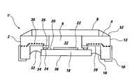
- FIG. 1is a perspective top view of a leadless image sensor package 1 of the present invention showing features which are common to the various embodiments of the invention.
- a package shell 2includes a top surface 4 having an aperture 6 extending downwardly through package shell 2 . While it is presently preferred that package shell 2 be constructed of a ceramic material, other materials such as molded plastic could also be used if capable of maintaining package tolerances and providing sufficient insulation from environmental conditions. The hermetic properties of a ceramic shell are particularly suited to the second embodiment of the present invention which is described in detail below.
- a transparent lid 8covers aperture 6 .
- the term “transparent”is used broadly herein to include materials that allow the passage of visible light or other forms of radiation having a selected wavelength such as infrared or ultraviolet.
- Example materials for transparent lid 8are plates of borosilicate or quartz glass; however, other glass, ceramic or plastic materials having suitable transmissivity are within the scope of the present invention.
- a plurality of castellated solder pads 10is formed around the periphery of package shell 2 , extending from a lower portion of package shell 2 side surfaces 12 onto the bottom surface 14 of the package shell 2 ( FIG. 2 ) for mechanical attachment and electrical coupling of the image sensor package 1 to a carrier substrate such as a printed circuit board (PCB).
- PCBprinted circuit board
- solder pads 10provide conductive bonds between image sensor package 1 and conductive elements 102 on carrier substrate 100 which may be easily inspected, and reworked and repaired if necessary. Solder pads 10 may be bonded to conductive elements 102 using reflowed tin/lead or silver solder, conductive or conductor-filled epoxy or other conductive bonding agents 104 which are well known in the art.
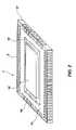
- FIG. 2is a perspective bottom view of the leadless image sensor package 1 showing further features common to the embodiments of the invention.
- a bottom-side cavity 16is formed in bottom surface 14 of package shell 2 and is in communication with aperture 6 .
- An image sensor chip 18is flip-chip mounted within bottom-side cavity 16 in a face-up manner such that at least a portion of its active surface 20 ( FIG. 1 ) containing sensing circuitry is exposed through aperture 6 .
- active surface 20 of image sensor chip 18may receive light or other forms of radiation passed through transparent lid 8 .
- FIGS. 4 and 5A through 5 Ga first exemplary embodiment of the present invention and method of assembly thereof is illustrated.
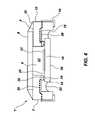
- FIG. 4shows a sectional side view of an image sensor package 1 ′ including image sensor chip 18 mounted to package shell 2 in a flip-chip fashion such that active surface 20 faces aperture 6 .
- active surface 20may optionally include pixeled microlenses 22 which cover the sensing circuitry thereon to focus light or provide other optical functions.
- Image sensor chip 18is mounted by attaching conductive bumps 24 disposed on bond pads or redistributed bond pads (not shown) on active surface 20 to terminal pads 26 formed on the top surface 28 of bottom-side cavity 16 and surrounding aperture 6 .
- Conductive bumps 24 and terminal pads 26are formed of, or plated with, gold that is joined to provide the presently preferred gold—gold interconnect bonding.
- Terminal pads 26are electrically connected to solder pads 10 via conductive lines or traces 30 buried within the ceramic material of package shell 2 .
- An encapsulant material 32fills aperture 6 , covering active surface 20 and pixeled microlenses 22 .
- Encapsulant 32serves to bond image sensor chip 18 to package shell 2 , maintain bond integrity between conductive bumps 24 and terminal pads 26 , and to protect the sides 34 of image sensor chip 18 .
- Encapsulant 32extends up to the top of aperture 6 where transparent lid 8 is mounted on top surface 4 of package shell 2 to cover aperture 6 .
- a layer of encapsulant 32further extends under and around the edges of transparent lid 8 to adhesively bond it in place on top surface 4 .
- Encapsulant 32may be a clear epoxy or other resin-type material like polymethylmethacrylate, polycarbonate or silicone, as long as it is suitably transmissive of light or other forms of radiation specific to the operation of image sensor chip 18 and is capable of adhesively bonding transparent lid 8 .
- the sides 34 of image sensor chip 18are partially encased in encapsulant 32 while the back 36 of image sensor chip 18 is left exposed. This encapsulation arrangement is acceptable for image sensor devices not likely to be subjected to extreme environmental conditions, and results in a simple and cost-effective package.
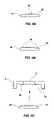
- FIGS. 5A through 5Gshow a method of assembly for the first exemplary embodiment of the present invention.
- FIG. 5Ashows an image sensor chip 18 having pixeled microlenses 22 on active surface 20 .
- gold or gold-plated conductive bumps 24are formed on active surface 20 for subsequently effecting gold—gold interconnect bonding.
- Image sensor chip 18is placed in bottom-side cavity 16 of package shell 2 with active surface 20 facing aperture 6 , as illustrated by FIG. 5C .
- conductive bumps 24are bonded to terminal pads 26 using known bonding techniques, effectively mounting image sensor chip 18 within package shell 2 and providing electrical connection of image sensor chip 18 to solder pads 10 through conductive lines or traces 30 ( FIG. 4 ).
- FIG. 5Ashows an image sensor chip 18 having pixeled microlenses 22 on active surface 20 .
- gold or gold-plated conductive bumps 24are formed on active surface 20 for subsequently effecting gold—gold interconnect bonding.
- Image sensor chip 18is placed in bottom-side cavity 16 of package shell
- FIG. 5Eshows encapsulant 32 deposited within aperture 6 and over a central portion of the top surface 4 of package shell 2 .
- transparent lid 8is lowered onto the top of encapsulant 32 and gradually squeezed into contact with top surface 4 , as illustrated in FIG. 5G .
- FIG. 5Gwhen transparent lid 8 is squeezed into place, it forces encapsulant 32 through spaces between the bonded conductive bumps 24 and terminal pads 26 and out into bottom-side cavity 16 to partially encase the sides 34 of image sensor chip 18 .
- Encapsulant 32is also forced out around the edges of transparent lid 8 to further hold it in place on top surface 4 .
- Encapsulant 32is then allowed to cure or, in the case of an activated adhesive material, may be set using UV radiation, thermal, chemical or other appropriate curing processes.
- image sensor package 1 ′is completely assembled and ready for attachment to carrier substrate 100 .
- FIG. 5Hwhich corresponds to the actions taken in FIG. 5E , shows this alternative to the method.
- encapsulant 32is deposited within aperture 6 and over a central portion of the top surface 4 of package shell 2 .
- FIG. 5Hshows the process is then paused for a period of time to allow encapsulant 32 to flow into bottom-side cavity 16 by capillary action prior to the placement of transparent lid 8 .
- the placement of transparent lid 8 depicted in FIG. 5Fis conducted in the same manner as before.
- FIGS. 6 and 7 A through 7 Ha second exemplary embodiment of the present invention that addresses these issues is illustrated.
- FIG. 6shows a sectional side view of an image sensor package 1 ′′ wherein package shell 2 is prefabricated with transparent lid 8 in place.
- a depression or recess 38may be formed in top surface 4 of package shell 2 to seat transparent lid 8 .
- transparent lid 8is a glass or ceramic material, it may be integrally formed with the presently preferred ceramic material of package shell 2 during a ceramic firing process. This approach provides a unitary component with a hermetically sealed top surface 4 .
- Various adhesivesmay also be used to attach transparent lid 8 to package shell 2 as long as they supply a strong, hermetic bond without significantly impinging into aperture 6 .
- Image sensor chip 18is still mounted to package shell 2 by flip-chip bonding of conductive bumps 24 and terminal pads 26 , but an encapsulant material is not deposited within aperture 6 to cover active surface 20 due to the optical requirements of image sensor chip 18 .
- Mechanical integrity and sealing of image sensor chip 18is instead maintained by the hermetic seal between transparent lid 8 and package shell 2 formed during prefabrication and by a backing cap 40 , which will be described in detail below.
- Castellated solder pads 10have the same configuration as those of the first embodiment and are similarly electrically connected to the interconnect bonds via conductive lines or traces 30 buried within the material of package shell 2 .
- a ceramic backing cap 40is placed over bottom-side cavity 16 to cover the sides 34 and back 36 of image sensor chip 18 .
- Backing cap 40is seated on a peripheral ledge surface 42 formed in bottom surface 14 of package shell 2 around the periphery of bottom-side cavity 16 .
- a bead of epoxy or other adhesive material 44may be used to hold backing cap 40 in place and hermetically seal the assembly.
- Compression member 46is formed on backing cap 40 and makes contact with the perimeter of back 36 of image sensor chip 18 . By providing force to the back 36 of image sensor chip 18 , compression member 46 helps to maintain mechanical integrity of the interconnect bond between conductive bumps 24 and terminal pads 26 and adds a cushion between backing cap 40 and image sensor chip 118 .
- compression member 46is a soft gold trace formed on backing cap 40 ; however, other materials having similar compressive and sealing properties are within the scope of the invention. Further, while compression member 46 is depicted as contacting only the perimeter of back 36 of image sensor chip 18 , other arrangements such as configuring compression member 46 to contact the entire back 36 are possible.
- FIGS. 7A through 7Hshow a method of assembly for the second exemplary embodiment of the present invention.
- FIG. 7Ashows an image sensor chip 18 having pixeled microlenses 22 on active surface 20
- FIG. 7Bshows the formation of gold or gold-plated conductive bumps 24 thereon for effecting gold—gold interconnect bonding as in the first image sensor package 1 ′ embodiment.
- Image sensor chip 18is placed in bottom-side cavity 16 of package shell 2 with active surface 20 facing aperture 6 , as illustrated by FIG. 7C .
- package shell 2has been prefabricated with transparent lid 8 already in place, providing a strong, hermetic seal that does not require a subsequent deposition of encapsulant material.
- transparent lid 8already in place
- FIG. 7Dshows conductive bumps 24 are bonded to terminal pads 26 , mounting image sensor chip 18 within package shell 2 and providing electrical connection of image sensor chip 18 to solder pads 10 through conductive lines or traces 30 ( FIG. 6 ).
- FIG. 7Eshows backing cap 40 with compression member 46 formed thereon.
- FIG. 7Fa bead of epoxy or other adhesive material 44 is dispensed around the perimeter of backing cap 40 .
- Backing cap 40is then pressed into contact with peripheral ledge surface 42 and compression member 46 is deformably compressed by the back 36 of image sensor chip 18 , as illustrated by FIGS. 7G and 7H .
- Image sensor chip 18is hermetically sealed within image sensor package 1 ′′, which is now ready for attachment to carrier substrate 100 .
- the backing cap 40 of the second embodiment image sensor package 1 ′′might be included in the first embodiment image sensor package 1 ′ in order to further hermetically seal the device.
- compression member 46may not be required on backing cap 40 , as image sensor chip 18 would already be secured by encapsulant 32 .
- the above-illustrated exemplary embodiments of the present inventionprovide compact leadless packaging for an image sensor or other optically interactive microelectronic device that is simple and economical to fabricate. These image sensor package embodiments are also well suited for a range of environmental conditions, allowing a specific package configuration to be selected based on utility versus cost considerations.
- the present inventionhas been depicted and described with respect to the illustrated embodiments, various additions, deletions and modifications are contemplated within its scope or essential characteristics.
- the inventionhas utility for the packaging of numerous types of optically interactive microelectronic devices.
- the scope of the present inventionis, therefore, indicated by the appended claims rather than the foregoing description. All changes which come within the meaning and range of equivalency of the claims are to be embraced within their scope.
Landscapes
- Solid State Image Pick-Up Elements (AREA)
Abstract
Description
Claims (24)
Priority Applications (3)
| Application Number | Priority Date | Filing Date | Title |
|---|---|---|---|
| US10/233,319US7274094B2 (en) | 2002-08-28 | 2002-08-28 | Leadless packaging for image sensor devices |
| SG200702173-6ASG146474A1 (en) | 2002-08-28 | 2002-10-03 | Leadless packaging for image sensor devices |
| US10/693,376US7112471B2 (en) | 2002-08-28 | 2003-10-23 | Leadless packaging for image sensor devices and methods of assembly |
Applications Claiming Priority (1)
| Application Number | Priority Date | Filing Date | Title |
|---|---|---|---|
| US10/233,319US7274094B2 (en) | 2002-08-28 | 2002-08-28 | Leadless packaging for image sensor devices |
Related Child Applications (1)
| Application Number | Title | Priority Date | Filing Date |
|---|---|---|---|
| US10/693,376DivisionUS7112471B2 (en) | 2002-08-28 | 2003-10-23 | Leadless packaging for image sensor devices and methods of assembly |
Publications (2)
| Publication Number | Publication Date |
|---|---|
| US20040041221A1 US20040041221A1 (en) | 2004-03-04 |
| US7274094B2true US7274094B2 (en) | 2007-09-25 |
Family
ID=31977212
Family Applications (2)
| Application Number | Title | Priority Date | Filing Date |
|---|---|---|---|
| US10/233,319Expired - LifetimeUS7274094B2 (en) | 2002-08-28 | 2002-08-28 | Leadless packaging for image sensor devices |
| US10/693,376Expired - LifetimeUS7112471B2 (en) | 2002-08-28 | 2003-10-23 | Leadless packaging for image sensor devices and methods of assembly |
Family Applications After (1)
| Application Number | Title | Priority Date | Filing Date |
|---|---|---|---|
| US10/693,376Expired - LifetimeUS7112471B2 (en) | 2002-08-28 | 2003-10-23 | Leadless packaging for image sensor devices and methods of assembly |
Country Status (2)
| Country | Link |
|---|---|
| US (2) | US7274094B2 (en) |
| SG (1) | SG146474A1 (en) |
Cited By (19)
| Publication number | Priority date | Publication date | Assignee | Title |
|---|---|---|---|---|
| US20040252992A1 (en)* | 2003-04-10 | 2004-12-16 | Hunter Andrew Arthur | Digital camera with removable imaging module |
| US20060035415A1 (en)* | 2004-08-16 | 2006-02-16 | Wood Alan G | Frame structure and semiconductor attach process for use therewith for fabrication of image sensor packages and the like, and resulting packages |
| US20070041163A1 (en)* | 2003-03-03 | 2007-02-22 | Wavecom | Method for producing an electronic component or module and a corresponding component or module |
| US20080085038A1 (en)* | 2006-10-05 | 2008-04-10 | Chipmos Technologies (Bermuda) Ltd. | Flim type package for fingerprint sensor |
| US20080246140A1 (en)* | 2004-12-28 | 2008-10-09 | Kabushiki Kaisha Toshiba | Semiconductor device |
| US20090097139A1 (en)* | 2007-10-15 | 2009-04-16 | Masanori Minamio | Optical device and manufacturing method thereof |
| US20090179290A1 (en)* | 2008-01-15 | 2009-07-16 | Huang Shuangwu | Encapsulated imager packaging |
| US20100087024A1 (en)* | 2008-06-19 | 2010-04-08 | Noureddine Hawat | Device cavity organic package structures and methods of manufacturing same |
| US20100117083A1 (en)* | 2003-03-27 | 2010-05-13 | Panasonic Corporation | Semiconductor device |
| US20100193240A1 (en)* | 2009-02-04 | 2010-08-05 | Yoshiki Takayama | Device |
| US7911017B1 (en)* | 2005-07-07 | 2011-03-22 | Amkor Technology, Inc. | Direct glass attached on die optical module |
| US20130056844A1 (en)* | 2011-09-02 | 2013-03-07 | Vage Oganesian | Stepped Package For Image Sensor And Method Of Making Same |
| US20130286281A1 (en)* | 2012-04-27 | 2013-10-31 | Canon Kabushiki Kaisha | Image pickup apparatus having image pickup device |
| US20130285243A1 (en)* | 2012-04-27 | 2013-10-31 | Hon Hai Precision Industry Co., Ltd. | Easily assembled chip assembly and chip assembling method |
| US9496247B2 (en) | 2013-08-26 | 2016-11-15 | Optiz, Inc. | Integrated camera module and method of making same |
| US20180315894A1 (en)* | 2017-04-26 | 2018-11-01 | Advanced Semiconductor Engineering, Inc. | Semiconductor device package and a method of manufacturing the same |
| US20190035836A1 (en)* | 2016-02-01 | 2019-01-31 | Sony Corporation | Image sensor package and imaging apparatus |
| US20190074617A1 (en)* | 2016-04-25 | 2019-03-07 | Hewlett Packard Enterprise Development Lp | Sockets including wicking regions |
| US10714526B2 (en)* | 2013-12-13 | 2020-07-14 | Sony Corporation | Solid-state imaging device, manufacturing method thereof, and electronic apparatus |
Families Citing this family (46)
| Publication number | Priority date | Publication date | Assignee | Title |
|---|---|---|---|---|
| US7012315B1 (en)* | 2000-11-01 | 2006-03-14 | Micron Technology, Inc. | Frame scale package using contact lines through the elements |
| US6843421B2 (en)* | 2001-08-13 | 2005-01-18 | Matrix Semiconductor, Inc. | Molded memory module and method of making the module absent a substrate support |
| TW544882B (en) | 2001-12-31 | 2003-08-01 | Megic Corp | Chip package structure and process thereof |
| TW503496B (en) | 2001-12-31 | 2002-09-21 | Megic Corp | Chip packaging structure and manufacturing process of the same |
| US6673698B1 (en)* | 2002-01-19 | 2004-01-06 | Megic Corporation | Thin film semiconductor package utilizing a glass substrate with composite polymer/metal interconnect layers |
| TW584950B (en) | 2001-12-31 | 2004-04-21 | Megic Corp | Chip packaging structure and process thereof |
| TW517361B (en) | 2001-12-31 | 2003-01-11 | Megic Corp | Chip package structure and its manufacture process |
| US6982470B2 (en)* | 2002-11-27 | 2006-01-03 | Seiko Epson Corporation | Semiconductor device, method of manufacturing the same, cover for semiconductor device, and electronic equipment |
| US7199438B2 (en)* | 2003-09-23 | 2007-04-03 | Advanced Semiconductor Engineering, Inc. | Overmolded optical package |
| JP4170950B2 (en) | 2003-10-10 | 2008-10-22 | 松下電器産業株式会社 | Optical device and manufacturing method thereof |
| KR100541654B1 (en)* | 2003-12-02 | 2006-01-12 | 삼성전자주식회사 | Wiring board and semiconductor device for solid-state imaging using same |
| JP4421934B2 (en)* | 2004-04-30 | 2010-02-24 | 株式会社ルネサステクノロジ | Manufacturing method of semiconductor device |
| US7547978B2 (en) | 2004-06-14 | 2009-06-16 | Micron Technology, Inc. | Underfill and encapsulation of semiconductor assemblies with materials having differing properties |
| US20060016973A1 (en)* | 2004-07-21 | 2006-01-26 | Advanced Semiconductor Engineering, Inc. | Multi-chip image sensor package module |
| US7235431B2 (en) | 2004-09-02 | 2007-06-26 | Micron Technology, Inc. | Methods for packaging a plurality of semiconductor dice using a flowable dielectric material |
| NL1028253C2 (en)* | 2005-02-11 | 2006-08-14 | Uteke Maria Klaassens | Sensor microchip with contact ring, image recording sensor, image recording camera. |
| US20060180909A1 (en)* | 2005-02-14 | 2006-08-17 | Irwin Kim | Optical device package |
| JP2006245246A (en)* | 2005-03-02 | 2006-09-14 | Sharp Corp | Solid-state imaging device |
| TW200644261A (en)* | 2005-06-06 | 2006-12-16 | Megica Corp | Chip-package structure and manufacturing process thereof |
| US20070090284A1 (en)* | 2005-10-20 | 2007-04-26 | Ho Mon N | Image sensor package structure |
| JP2007299929A (en)* | 2006-04-28 | 2007-11-15 | Matsushita Electric Ind Co Ltd | Optical device apparatus and optical device module using the same |
| USD565207S1 (en)* | 2006-06-20 | 2008-03-25 | Matsushita Electric Industrial Co., Ltd. | Lighting apparatus |
| USD569529S1 (en)* | 2006-06-20 | 2008-05-20 | Matsushita Electric Industrial Co., Ltd. | Lighting apparatus |
| USD611628S1 (en)* | 2006-06-20 | 2010-03-09 | Panasonic Corporation | Lighting apparatus |
| USD572387S1 (en)* | 2006-06-20 | 2008-07-01 | Matsushita Electric Industrial Co., Ltd. | Lighting apparatus |
| US7920086B2 (en)* | 2006-07-07 | 2011-04-05 | Honeywell International Inc. | Display for displaying compressed video |
| US7602427B2 (en)* | 2006-07-07 | 2009-10-13 | Honeywell International Inc. | Image sensor that provides raw output comprising compressed data |
| US20080007550A1 (en)* | 2006-07-07 | 2008-01-10 | Honeywell International, Inc. | Current driven display for displaying compressed video |
| US20080018624A1 (en)* | 2006-07-07 | 2008-01-24 | Honeywell International, Inc. | Display for displaying compressed video based on sub-division area |
| US20080007637A1 (en)* | 2006-07-07 | 2008-01-10 | Honeywell International, Inc. | Image sensor that provides compressed data based on junction area |
| JP4955349B2 (en)* | 2006-09-07 | 2012-06-20 | 新光電気工業株式会社 | Semiconductor device |
| GB2446185A (en)* | 2006-10-30 | 2008-08-06 | Sensl Technologies Ltd | Optical assembly and method of assembly |
| USD572388S1 (en)* | 2006-12-19 | 2008-07-01 | Matsushita Electric Industrial Co., Ltd. | Lighting apparatus |
| SG148056A1 (en) | 2007-05-17 | 2008-12-31 | Micron Technology Inc | Integrated circuit packages, methods of forming integrated circuit packages, and methods of assembling intgrated circuit packages |
| US7786563B1 (en)* | 2007-06-28 | 2010-08-31 | Virtium Technology, Inc. | Stacking multiple devices using single-piece interconnecting element |
| US7993977B2 (en)* | 2007-07-02 | 2011-08-09 | Micron Technology, Inc. | Method of forming molded standoff structures on integrated circuit devices |
| SG149709A1 (en)* | 2007-07-12 | 2009-02-27 | Micron Technology Inc | Microelectronic imagers and methods of manufacturing such microelectronic imagers |
| US7923298B2 (en) | 2007-09-07 | 2011-04-12 | Micron Technology, Inc. | Imager die package and methods of packaging an imager die on a temporary carrier |
| US8319114B2 (en)* | 2008-04-02 | 2012-11-27 | Densel Lambda K.K. | Surface mount power module dual footprint |
| SG142321A1 (en)* | 2008-04-24 | 2009-11-26 | Micron Technology Inc | Pre-encapsulated cavity interposer |
| JP5430027B2 (en)* | 2010-08-04 | 2014-02-26 | パナソニック株式会社 | Solid-state imaging device |
| JP5709165B2 (en)* | 2011-03-10 | 2015-04-30 | セイコーインスツル株式会社 | Optical device |
| JP5925432B2 (en)* | 2011-05-10 | 2016-05-25 | エスアイアイ・セミコンダクタ株式会社 | Optical sensor and optical sensor manufacturing method |
| JP6409575B2 (en)* | 2013-01-30 | 2018-10-24 | パナソニック株式会社 | Multilayer semiconductor device |
| KR102005351B1 (en)* | 2017-12-07 | 2019-07-31 | 삼성전자주식회사 | Fan-out sensor package |
| US12074182B2 (en) | 2018-08-21 | 2024-08-27 | Sony Semiconductor Solutions Corporation | Semiconductor device, electronic apparatus, and method for manufacturing semiconductor device |
Citations (33)
| Publication number | Priority date | Publication date | Assignee | Title |
|---|---|---|---|---|
| US5357056A (en) | 1992-03-23 | 1994-10-18 | Nec Corporation | Chip carrier for optical device |
| US5477081A (en)* | 1991-03-29 | 1995-12-19 | Mitsubishi Denki Kabushiki Kaisha | Semiconductor device package |
| US5675474A (en)* | 1994-07-15 | 1997-10-07 | Mitsubishi Materials Corporation | Highly heat-radiating ceramic package |
| US5687474A (en)* | 1992-04-30 | 1997-11-18 | Vlsi Technology, Inc. | Method of assembling and cooling a package structure with accessible chip |
| US5699073A (en) | 1996-03-04 | 1997-12-16 | Motorola | Integrated electro-optical package with carrier ring and method of fabrication |
| US5702985A (en) | 1992-06-26 | 1997-12-30 | Staktek Corporation | Hermetically sealed ceramic integrated circuit heat dissipating package fabrication method |
| US5867368A (en) | 1997-09-09 | 1999-02-02 | Amkor Technology, Inc. | Mounting for a semiconductor integrated circuit device |
| US5865935A (en) | 1995-02-02 | 1999-02-02 | Eastman Kodak Company | Method of packaging image sensors |
| US6147389A (en) | 1999-06-04 | 2000-11-14 | Silicon Film Technologies, Inc. | Image sensor package with image plane reference |
| US6351027B1 (en) | 2000-02-29 | 2002-02-26 | Agilent Technologies, Inc. | Chip-mounted enclosure |
| US20020024131A1 (en)* | 1997-07-10 | 2002-02-28 | Keiji Sasano | Hollow package and method for fabricating the same and solid-state image apparatus provided therewith |
| US20020043706A1 (en)* | 2000-06-28 | 2002-04-18 | Institut National D'optique | Miniature Microdevice Package and Process for Making Thereof |
| US6384473B1 (en) | 2000-05-16 | 2002-05-07 | Sandia Corporation | Microelectronic device package with an integral window |
| US6404648B1 (en)* | 2001-03-30 | 2002-06-11 | Hewlett-Packard Co. | Assembly and method for constructing a multi-die integrated circuit |
| US20020089044A1 (en)* | 2001-01-09 | 2002-07-11 | 3M Innovative Properties Company | Hermetic mems package with interlocking layers |
| US6433332B1 (en) | 2000-09-26 | 2002-08-13 | Rockwell Automation Technologies, Inc. | Protective encapsulation for a phototransducer including a surfactant film |
| US6455927B1 (en) | 2001-03-12 | 2002-09-24 | Amkor Technology, Inc. | Micromirror device package |
| US6531341B1 (en)* | 2000-05-16 | 2003-03-11 | Sandia Corporation | Method of fabricating a microelectronic device package with an integral window |
| US20030056967A1 (en)* | 1999-12-08 | 2003-03-27 | Glenn Thomas P. | Method of fabricating and using an image sensor package |
| US6545332B2 (en)* | 2001-01-17 | 2003-04-08 | Siliconware Precision Industries Co., Ltd. | Image sensor of a quad flat package |
| US20030111441A1 (en)* | 2000-06-28 | 2003-06-19 | Institut National D'optique | Miniature microdevice package and process for making thereof |
| US20030197285A1 (en)* | 2002-04-23 | 2003-10-23 | Kulicke & Soffa Investments, Inc. | High density substrate for the packaging of integrated circuits |
| US6649991B1 (en)* | 2002-04-22 | 2003-11-18 | Scientek Corp. | Image sensor semiconductor package |
| US6686588B1 (en)* | 2001-01-16 | 2004-02-03 | Amkor Technology, Inc. | Optical module with lens integral holder |
| US20040038442A1 (en) | 2002-08-26 | 2004-02-26 | Kinsman Larry D. | Optically interactive device packages and methods of assembly |
| US6703598B2 (en) | 2000-04-11 | 2004-03-09 | Hamamatsu Photonics K.K. | Semiconductor photo-detecting apparatus |
| US6713876B1 (en)* | 1999-11-04 | 2004-03-30 | Stmicroelectronics S.A. | Optical semiconductor housing and method for making same |
| US6798031B2 (en)* | 2001-02-28 | 2004-09-28 | Fujitsu Limited | Semiconductor device and method for making the same |
| US20040212055A1 (en)* | 2001-05-18 | 2004-10-28 | Juan Exposito | Shielded housing for optical semiconductor component |
| US20040217454A1 (en)* | 2001-05-18 | 2004-11-04 | Remi Brechignac | Optical semiconductor package with incorporated lens and shielding |
| US6861737B1 (en)* | 1996-12-30 | 2005-03-01 | Samsung Electronics Co., Ltd. | Semiconductor device packages having semiconductor chips attached to circuit boards, and stack packages using the same |
| US6885107B2 (en) | 2002-08-29 | 2005-04-26 | Micron Technology, Inc. | Flip-chip image sensor packages and methods of fabrication |
| US7012315B1 (en)* | 2000-11-01 | 2006-03-14 | Micron Technology, Inc. | Frame scale package using contact lines through the elements |
- 2002
- 2002-08-28USUS10/233,319patent/US7274094B2/ennot_activeExpired - Lifetime
- 2002-10-03SGSG200702173-6Apatent/SG146474A1/enunknown
- 2003
- 2003-10-23USUS10/693,376patent/US7112471B2/ennot_activeExpired - Lifetime
Patent Citations (33)
| Publication number | Priority date | Publication date | Assignee | Title |
|---|---|---|---|---|
| US5477081A (en)* | 1991-03-29 | 1995-12-19 | Mitsubishi Denki Kabushiki Kaisha | Semiconductor device package |
| US5357056A (en) | 1992-03-23 | 1994-10-18 | Nec Corporation | Chip carrier for optical device |
| US5687474A (en)* | 1992-04-30 | 1997-11-18 | Vlsi Technology, Inc. | Method of assembling and cooling a package structure with accessible chip |
| US5702985A (en) | 1992-06-26 | 1997-12-30 | Staktek Corporation | Hermetically sealed ceramic integrated circuit heat dissipating package fabrication method |
| US5675474A (en)* | 1994-07-15 | 1997-10-07 | Mitsubishi Materials Corporation | Highly heat-radiating ceramic package |
| US5865935A (en) | 1995-02-02 | 1999-02-02 | Eastman Kodak Company | Method of packaging image sensors |
| US5699073A (en) | 1996-03-04 | 1997-12-16 | Motorola | Integrated electro-optical package with carrier ring and method of fabrication |
| US6861737B1 (en)* | 1996-12-30 | 2005-03-01 | Samsung Electronics Co., Ltd. | Semiconductor device packages having semiconductor chips attached to circuit boards, and stack packages using the same |
| US20020024131A1 (en)* | 1997-07-10 | 2002-02-28 | Keiji Sasano | Hollow package and method for fabricating the same and solid-state image apparatus provided therewith |
| US5867368A (en) | 1997-09-09 | 1999-02-02 | Amkor Technology, Inc. | Mounting for a semiconductor integrated circuit device |
| US6147389A (en) | 1999-06-04 | 2000-11-14 | Silicon Film Technologies, Inc. | Image sensor package with image plane reference |
| US6713876B1 (en)* | 1999-11-04 | 2004-03-30 | Stmicroelectronics S.A. | Optical semiconductor housing and method for making same |
| US20030056967A1 (en)* | 1999-12-08 | 2003-03-27 | Glenn Thomas P. | Method of fabricating and using an image sensor package |
| US6351027B1 (en) | 2000-02-29 | 2002-02-26 | Agilent Technologies, Inc. | Chip-mounted enclosure |
| US6703598B2 (en) | 2000-04-11 | 2004-03-09 | Hamamatsu Photonics K.K. | Semiconductor photo-detecting apparatus |
| US6384473B1 (en) | 2000-05-16 | 2002-05-07 | Sandia Corporation | Microelectronic device package with an integral window |
| US6531341B1 (en)* | 2000-05-16 | 2003-03-11 | Sandia Corporation | Method of fabricating a microelectronic device package with an integral window |
| US20030111441A1 (en)* | 2000-06-28 | 2003-06-19 | Institut National D'optique | Miniature microdevice package and process for making thereof |
| US20020043706A1 (en)* | 2000-06-28 | 2002-04-18 | Institut National D'optique | Miniature Microdevice Package and Process for Making Thereof |
| US6433332B1 (en) | 2000-09-26 | 2002-08-13 | Rockwell Automation Technologies, Inc. | Protective encapsulation for a phototransducer including a surfactant film |
| US7012315B1 (en)* | 2000-11-01 | 2006-03-14 | Micron Technology, Inc. | Frame scale package using contact lines through the elements |
| US20020089044A1 (en)* | 2001-01-09 | 2002-07-11 | 3M Innovative Properties Company | Hermetic mems package with interlocking layers |
| US6686588B1 (en)* | 2001-01-16 | 2004-02-03 | Amkor Technology, Inc. | Optical module with lens integral holder |
| US6545332B2 (en)* | 2001-01-17 | 2003-04-08 | Siliconware Precision Industries Co., Ltd. | Image sensor of a quad flat package |
| US6798031B2 (en)* | 2001-02-28 | 2004-09-28 | Fujitsu Limited | Semiconductor device and method for making the same |
| US6455927B1 (en) | 2001-03-12 | 2002-09-24 | Amkor Technology, Inc. | Micromirror device package |
| US6404648B1 (en)* | 2001-03-30 | 2002-06-11 | Hewlett-Packard Co. | Assembly and method for constructing a multi-die integrated circuit |
| US20040212055A1 (en)* | 2001-05-18 | 2004-10-28 | Juan Exposito | Shielded housing for optical semiconductor component |
| US20040217454A1 (en)* | 2001-05-18 | 2004-11-04 | Remi Brechignac | Optical semiconductor package with incorporated lens and shielding |
| US6649991B1 (en)* | 2002-04-22 | 2003-11-18 | Scientek Corp. | Image sensor semiconductor package |
| US20030197285A1 (en)* | 2002-04-23 | 2003-10-23 | Kulicke & Soffa Investments, Inc. | High density substrate for the packaging of integrated circuits |
| US20040038442A1 (en) | 2002-08-26 | 2004-02-26 | Kinsman Larry D. | Optically interactive device packages and methods of assembly |
| US6885107B2 (en) | 2002-08-29 | 2005-04-26 | Micron Technology, Inc. | Flip-chip image sensor packages and methods of fabrication |
Cited By (39)
| Publication number | Priority date | Publication date | Assignee | Title |
|---|---|---|---|---|
| US20070041163A1 (en)* | 2003-03-03 | 2007-02-22 | Wavecom | Method for producing an electronic component or module and a corresponding component or module |
| US8456024B2 (en) | 2003-03-27 | 2013-06-04 | Panasonic Corporation | Semiconductor device having a pad-disposition restriction area |
| US7847418B2 (en)* | 2003-03-27 | 2010-12-07 | Panasonic Corporation | Semiconductor device |
| US8212366B2 (en)* | 2003-03-27 | 2012-07-03 | Panasonic Corporation | Semiconductor device |
| US20100117083A1 (en)* | 2003-03-27 | 2010-05-13 | Panasonic Corporation | Semiconductor device |
| US20110037173A1 (en)* | 2003-03-27 | 2011-02-17 | Panasonic Corporation | Semiconductor device |
| US20040252992A1 (en)* | 2003-04-10 | 2004-12-16 | Hunter Andrew Arthur | Digital camera with removable imaging module |
| US20060192230A1 (en)* | 2004-08-16 | 2006-08-31 | Wood Alan G | Image sensor packages and frame structure thereof |
| US20060035415A1 (en)* | 2004-08-16 | 2006-02-16 | Wood Alan G | Frame structure and semiconductor attach process for use therewith for fabrication of image sensor packages and the like, and resulting packages |
| US7645635B2 (en) | 2004-08-16 | 2010-01-12 | Micron Technology, Inc. | Frame structure and semiconductor attach process for use therewith for fabrication of image sensor packages and the like, and resulting packages |
| US7791184B2 (en)* | 2004-08-16 | 2010-09-07 | Micron Technology, Inc. | Image sensor packages and frame structure thereof |
| US20080246140A1 (en)* | 2004-12-28 | 2008-10-09 | Kabushiki Kaisha Toshiba | Semiconductor device |
| US7576423B2 (en)* | 2004-12-28 | 2009-08-18 | Kabushiki Kaisha Toshiba | Semiconductor device |
| US7911017B1 (en)* | 2005-07-07 | 2011-03-22 | Amkor Technology, Inc. | Direct glass attached on die optical module |
| US20080085038A1 (en)* | 2006-10-05 | 2008-04-10 | Chipmos Technologies (Bermuda) Ltd. | Flim type package for fingerprint sensor |
| US7936032B2 (en)* | 2006-10-05 | 2011-05-03 | Chipmos Technologies Inc. | Film type package for fingerprint sensor |
| US7939901B2 (en)* | 2007-10-15 | 2011-05-10 | Panasonic Corporation | Optical device for reducing disturbance light and manufacturing method thereof |
| US20090097139A1 (en)* | 2007-10-15 | 2009-04-16 | Masanori Minamio | Optical device and manufacturing method thereof |
| US20090179290A1 (en)* | 2008-01-15 | 2009-07-16 | Huang Shuangwu | Encapsulated imager packaging |
| US20100087024A1 (en)* | 2008-06-19 | 2010-04-08 | Noureddine Hawat | Device cavity organic package structures and methods of manufacturing same |
| US20100193240A1 (en)* | 2009-02-04 | 2010-08-05 | Yoshiki Takayama | Device |
| US8110755B2 (en)* | 2009-02-04 | 2012-02-07 | Panasonic Corporation | Package for an optical device |
| US20130056844A1 (en)* | 2011-09-02 | 2013-03-07 | Vage Oganesian | Stepped Package For Image Sensor And Method Of Making Same |
| US9373653B2 (en)* | 2011-09-02 | 2016-06-21 | Optiz, Inc. | Stepped package for image sensor |
| US20150200219A1 (en)* | 2011-09-02 | 2015-07-16 | Optiz, Inc. | Stepped Package For Image Sensor |
| US9018725B2 (en)* | 2011-09-02 | 2015-04-28 | Optiz, Inc. | Stepped package for image sensor and method of making same |
| KR101453158B1 (en)* | 2011-09-02 | 2014-10-27 | 옵티즈 인코포레이티드 | Stepped package for image sensor and method of making same |
| US8890326B2 (en)* | 2012-04-27 | 2014-11-18 | Hon Hai Precision Industry Co., Ltd. | Easily assembled chip assembly and chip assembling method |
| JP2013232732A (en)* | 2012-04-27 | 2013-11-14 | Canon Inc | Imaging device |
| US9065989B2 (en)* | 2012-04-27 | 2015-06-23 | Canon Kabushiki Kaisha | Image pickup apparatus having image pickup device |
| US20130285243A1 (en)* | 2012-04-27 | 2013-10-31 | Hon Hai Precision Industry Co., Ltd. | Easily assembled chip assembly and chip assembling method |
| US20130286281A1 (en)* | 2012-04-27 | 2013-10-31 | Canon Kabushiki Kaisha | Image pickup apparatus having image pickup device |
| US9496247B2 (en) | 2013-08-26 | 2016-11-15 | Optiz, Inc. | Integrated camera module and method of making same |
| US10714526B2 (en)* | 2013-12-13 | 2020-07-14 | Sony Corporation | Solid-state imaging device, manufacturing method thereof, and electronic apparatus |
| US20190035836A1 (en)* | 2016-02-01 | 2019-01-31 | Sony Corporation | Image sensor package and imaging apparatus |
| US11094722B2 (en)* | 2016-02-01 | 2021-08-17 | Sony Corporation | Image sensor package and imaging apparatus |
| US20190074617A1 (en)* | 2016-04-25 | 2019-03-07 | Hewlett Packard Enterprise Development Lp | Sockets including wicking regions |
| US11088479B2 (en)* | 2016-04-25 | 2021-08-10 | Hewlett Packard Enterprise Development Lp | Sockets including wicking regions mounted on a system board |
| US20180315894A1 (en)* | 2017-04-26 | 2018-11-01 | Advanced Semiconductor Engineering, Inc. | Semiconductor device package and a method of manufacturing the same |
Also Published As
| Publication number | Publication date |
|---|---|
| US20040041221A1 (en) | 2004-03-04 |
| US7112471B2 (en) | 2006-09-26 |
| US20040084741A1 (en) | 2004-05-06 |
| SG146474A1 (en) | 2008-10-30 |
Similar Documents
| Publication | Publication Date | Title |
|---|---|---|
| US7274094B2 (en) | Leadless packaging for image sensor devices | |
| US8097895B2 (en) | Electronic device package with an optical device | |
| US6906403B2 (en) | Sealed electronic device packages with transparent coverings | |
| KR100604190B1 (en) | Solid state imaging device, semiconductor wafer, optical device module, method of solid state imaging device fabrication, and method of optical device module fabrication | |
| KR100742177B1 (en) | Semiconductor package, method of fabricating the same and semiconductor package module for image sensor | |
| JP2006332680A (en) | Method for packaging an image sensor and packaged image sensor | |
| JPH09129780A (en) | IC package, optical sensor IC package, and assembling method thereof | |
| CN101159279A (en) | Semiconductor imaging element and manufacturing method thereof, semiconductor imaging element module and device | |
| JP2002329850A (en) | Chip size package and manufacturing method thereof | |
| CN209086962U (en) | For shielding the recognizer component and electronic equipment of lower optical finger print | |
| JP2006005612A (en) | Imaging module | |
| CN101521185A (en) | Package structure and process for optical chip | |
| KR20050120142A (en) | Camera module and method of fabricating the same using epoxy | |
| JP2004063764A (en) | Optical coupling semiconductor device and method of manufacturing the same | |
| JP2003115563A (en) | Electrical components and their manufacturing method | |
| KR19980036778A (en) | CCD chip package structure | |
| KR20020061224A (en) | semiconductor package and manufacturing method the same |
Legal Events
| Date | Code | Title | Description |
|---|---|---|---|
| AS | Assignment | Owner name:MICRON TECHNOLOGY, INC., IDAHO Free format text:ASSIGNMENT OF ASSIGNORS INTEREST;ASSIGNORS:BOON, SUAN JEUNG;CHIA, YONG POO;NEO, YONG LOO;AND OTHERS;REEL/FRAME:013503/0662;SIGNING DATES FROM 20021028 TO 20021029 | |
| FEPP | Fee payment procedure | Free format text:PAYOR NUMBER ASSIGNED (ORIGINAL EVENT CODE: ASPN); ENTITY STATUS OF PATENT OWNER: LARGE ENTITY | |
| STCF | Information on status: patent grant | Free format text:PATENTED CASE | |
| CC | Certificate of correction | ||
| FPAY | Fee payment | Year of fee payment:4 | |
| FPAY | Fee payment | Year of fee payment:8 | |
| AS | Assignment | Owner name:U.S. BANK NATIONAL ASSOCIATION, AS COLLATERAL AGENT, CALIFORNIA Free format text:SECURITY INTEREST;ASSIGNOR:MICRON TECHNOLOGY, INC.;REEL/FRAME:038669/0001 Effective date:20160426 Owner name:U.S. BANK NATIONAL ASSOCIATION, AS COLLATERAL AGEN Free format text:SECURITY INTEREST;ASSIGNOR:MICRON TECHNOLOGY, INC.;REEL/FRAME:038669/0001 Effective date:20160426 | |
| AS | Assignment | Owner name:MORGAN STANLEY SENIOR FUNDING, INC., AS COLLATERAL AGENT, MARYLAND Free format text:PATENT SECURITY AGREEMENT;ASSIGNOR:MICRON TECHNOLOGY, INC.;REEL/FRAME:038954/0001 Effective date:20160426 Owner name:MORGAN STANLEY SENIOR FUNDING, INC., AS COLLATERAL Free format text:PATENT SECURITY AGREEMENT;ASSIGNOR:MICRON TECHNOLOGY, INC.;REEL/FRAME:038954/0001 Effective date:20160426 | |
| AS | Assignment | Owner name:U.S. BANK NATIONAL ASSOCIATION, AS COLLATERAL AGENT, CALIFORNIA Free format text:CORRECTIVE ASSIGNMENT TO CORRECT THE REPLACE ERRONEOUSLY FILED PATENT #7358718 WITH THE CORRECT PATENT #7358178 PREVIOUSLY RECORDED ON REEL 038669 FRAME 0001. ASSIGNOR(S) HEREBY CONFIRMS THE SECURITY INTEREST;ASSIGNOR:MICRON TECHNOLOGY, INC.;REEL/FRAME:043079/0001 Effective date:20160426 Owner name:U.S. BANK NATIONAL ASSOCIATION, AS COLLATERAL AGEN Free format text:CORRECTIVE ASSIGNMENT TO CORRECT THE REPLACE ERRONEOUSLY FILED PATENT #7358718 WITH THE CORRECT PATENT #7358178 PREVIOUSLY RECORDED ON REEL 038669 FRAME 0001. ASSIGNOR(S) HEREBY CONFIRMS THE SECURITY INTEREST;ASSIGNOR:MICRON TECHNOLOGY, INC.;REEL/FRAME:043079/0001 Effective date:20160426 | |
| AS | Assignment | Owner name:JPMORGAN CHASE BANK, N.A., AS COLLATERAL AGENT, ILLINOIS Free format text:SECURITY INTEREST;ASSIGNORS:MICRON TECHNOLOGY, INC.;MICRON SEMICONDUCTOR PRODUCTS, INC.;REEL/FRAME:047540/0001 Effective date:20180703 Owner name:JPMORGAN CHASE BANK, N.A., AS COLLATERAL AGENT, IL Free format text:SECURITY INTEREST;ASSIGNORS:MICRON TECHNOLOGY, INC.;MICRON SEMICONDUCTOR PRODUCTS, INC.;REEL/FRAME:047540/0001 Effective date:20180703 | |
| AS | Assignment | Owner name:MICRON TECHNOLOGY, INC., IDAHO Free format text:RELEASE BY SECURED PARTY;ASSIGNOR:U.S. BANK NATIONAL ASSOCIATION, AS COLLATERAL AGENT;REEL/FRAME:047243/0001 Effective date:20180629 | |
| MAFP | Maintenance fee payment | Free format text:PAYMENT OF MAINTENANCE FEE, 12TH YEAR, LARGE ENTITY (ORIGINAL EVENT CODE: M1553); ENTITY STATUS OF PATENT OWNER: LARGE ENTITY Year of fee payment:12 | |
| AS | Assignment | Owner name:MICRON TECHNOLOGY, INC., IDAHO Free format text:RELEASE BY SECURED PARTY;ASSIGNOR:MORGAN STANLEY SENIOR FUNDING, INC., AS COLLATERAL AGENT;REEL/FRAME:050937/0001 Effective date:20190731 | |
| AS | Assignment | Owner name:MICRON SEMICONDUCTOR PRODUCTS, INC., IDAHO Free format text:RELEASE BY SECURED PARTY;ASSIGNOR:JPMORGAN CHASE BANK, N.A., AS COLLATERAL AGENT;REEL/FRAME:051028/0001 Effective date:20190731 Owner name:MICRON TECHNOLOGY, INC., IDAHO Free format text:RELEASE BY SECURED PARTY;ASSIGNOR:JPMORGAN CHASE BANK, N.A., AS COLLATERAL AGENT;REEL/FRAME:051028/0001 Effective date:20190731 |