US7274067B2 - Service programmable logic arrays with low tunnel barrier interpoly insulators - Google Patents
Service programmable logic arrays with low tunnel barrier interpoly insulatorsDownload PDFInfo
- Publication number
- US7274067B2 US7274067B2US11/202,460US20246005AUS7274067B2US 7274067 B2US7274067 B2US 7274067B2US 20246005 AUS20246005 AUS 20246005AUS 7274067 B2US7274067 B2US 7274067B2
- Authority
- US
- United States
- Prior art keywords
- programmable logic
- oxide
- logic array
- tunnel barrier
- floating gate
- Prior art date
- Legal status (The legal status is an assumption and is not a legal conclusion. Google has not performed a legal analysis and makes no representation as to the accuracy of the status listed.)
- Expired - Lifetime, expires
Links
- 230000004888barrier functionEffects0.000titleclaimsabstractdescription102
- 239000012212insulatorSubstances0.000titleclaimsabstractdescription89
- 238000003491arrayMethods0.000titleclaimsabstractdescription19
- 150000004706metal oxidesChemical class0.000claimsabstractdescription35
- 229910044991metal oxideInorganic materials0.000claimsabstractdescription33
- 239000000758substrateSubstances0.000claimsabstractdescription28
- YEXPOXQUZXUXJW-UHFFFAOYSA-Nlead(II) oxideInorganic materials[Pb]=OYEXPOXQUZXUXJW-UHFFFAOYSA-N0.000claimsabstract4
- 229910052751metalInorganic materials0.000claimsdescription72
- 239000002184metalSubstances0.000claimsdescription72
- 230000015654memoryEffects0.000claimsdescription61
- 229910021420polycrystalline siliconInorganic materials0.000claimsdescription34
- 238000007254oxidation reactionMethods0.000claimsdescription33
- 230000003647oxidationEffects0.000claimsdescription32
- TWNQGVIAIRXVLR-UHFFFAOYSA-Noxo(oxoalumanyloxy)alumaneChemical groupO=[Al]O[Al]=OTWNQGVIAIRXVLR-UHFFFAOYSA-N0.000claimsdescription26
- 229920005591polysiliconPolymers0.000claimsdescription15
- 239000000463materialSubstances0.000claimsdescription12
- 239000004065semiconductorSubstances0.000claimsdescription11
- 229910052782aluminiumInorganic materials0.000claimsdescription10
- XAGFODPZIPBFFR-UHFFFAOYSA-NaluminiumChemical compound[Al]XAGFODPZIPBFFR-UHFFFAOYSA-N0.000claimsdescription10
- 229910000314transition metal oxideInorganic materials0.000claimsdescription8
- 229910052723transition metalInorganic materials0.000claimsdescription6
- 150000003624transition metalsChemical class0.000claimsdescription6
- 239000013078crystalSubstances0.000claimsdescription2
- 239000007769metal materialSubstances0.000claimsdescription2
- 229910052758niobiumInorganic materials0.000claimsdescription2
- 229910052715tantalumInorganic materials0.000claimsdescription2
- RTAQQCXQSZGOHL-UHFFFAOYSA-NTitaniumChemical compound[Ti]RTAQQCXQSZGOHL-UHFFFAOYSA-N0.000claims1
- QCWXUUIWCKQGHC-UHFFFAOYSA-NZirconiumChemical compound[Zr]QCWXUUIWCKQGHC-UHFFFAOYSA-N0.000claims1
- 229910052746lanthanumInorganic materials0.000claims1
- FZLIPJUXYLNCLC-UHFFFAOYSA-Nlanthanum atomChemical compound[La]FZLIPJUXYLNCLC-UHFFFAOYSA-N0.000claims1
- 239000010955niobiumSubstances0.000claims1
- GUCVJGMIXFAOAE-UHFFFAOYSA-Nniobium atomChemical compound[Nb]GUCVJGMIXFAOAE-UHFFFAOYSA-N0.000claims1
- GUVRBAGPIYLISA-UHFFFAOYSA-Ntantalum atomChemical compound[Ta]GUVRBAGPIYLISA-UHFFFAOYSA-N0.000claims1
- 229910052719titaniumInorganic materials0.000claims1
- 239000010936titaniumSubstances0.000claims1
- 229910052726zirconiumInorganic materials0.000claims1
- 238000000034methodMethods0.000abstractdescription31
- ZKATWMILCYLAPD-UHFFFAOYSA-Nniobium pentoxideChemical compoundO=[Nb](=O)O[Nb](=O)=OZKATWMILCYLAPD-UHFFFAOYSA-N0.000abstractdescription12
- GWEVSGVZZGPLCZ-UHFFFAOYSA-NTitan oxideChemical compoundO=[Ti]=OGWEVSGVZZGPLCZ-UHFFFAOYSA-N0.000abstractdescription10
- MCMNRKCIXSYSNV-UHFFFAOYSA-NZirconium dioxideChemical compoundO=[Zr]=OMCMNRKCIXSYSNV-UHFFFAOYSA-N0.000abstractdescription10
- PBCFLUZVCVVTBY-UHFFFAOYSA-Ntantalum pentoxideInorganic materialsO=[Ta](=O)O[Ta](=O)=OPBCFLUZVCVVTBY-UHFFFAOYSA-N0.000abstractdescription6
- PNEYBMLMFCGWSK-UHFFFAOYSA-Naluminium oxideInorganic materials[O-2].[O-2].[O-2].[Al+3].[Al+3]PNEYBMLMFCGWSK-UHFFFAOYSA-N0.000abstract1
- 229910052593corundumInorganic materials0.000abstract1
- 229910001845yogo sapphireInorganic materials0.000abstract1
- 210000004027cellAnatomy0.000description49
- 239000010408filmSubstances0.000description39
- 230000006870functionEffects0.000description38
- 239000010410layerSubstances0.000description33
- 230000005641tunnelingEffects0.000description30
- 230000005684electric fieldEffects0.000description21
- HTUMBQDCCIXGCV-UHFFFAOYSA-Nlead oxideChemical compound[O-2].[Pb+2]HTUMBQDCCIXGCV-UHFFFAOYSA-N0.000description19
- XUIMIQQOPSSXEZ-UHFFFAOYSA-NSiliconChemical compound[Si]XUIMIQQOPSSXEZ-UHFFFAOYSA-N0.000description15
- 229910052710siliconInorganic materials0.000description15
- 239000010703siliconSubstances0.000description15
- 238000013459approachMethods0.000description13
- 210000000746body regionAnatomy0.000description13
- VYPSYNLAJGMNEJ-UHFFFAOYSA-NSilicium dioxideChemical compoundO=[Si]=OVYPSYNLAJGMNEJ-UHFFFAOYSA-N0.000description12
- QVGXLLKOCUKJST-UHFFFAOYSA-Natomic oxygenChemical compound[O]QVGXLLKOCUKJST-UHFFFAOYSA-N0.000description12
- 229910052760oxygenInorganic materials0.000description12
- 239000001301oxygenSubstances0.000description12
- 230000008569processEffects0.000description12
- 230000015572biosynthetic processEffects0.000description11
- 239000002784hot electronSubstances0.000description11
- 150000002739metalsChemical class0.000description11
- 238000002347injectionMethods0.000description9
- 239000007924injectionSubstances0.000description9
- 239000000203mixtureSubstances0.000description9
- 238000010586diagramMethods0.000description8
- 229910045601alloyInorganic materials0.000description7
- 239000000956alloySubstances0.000description7
- 235000012431wafersNutrition0.000description7
- 230000008901benefitEffects0.000description6
- 230000015556catabolic processEffects0.000description6
- 238000005516engineering processMethods0.000description6
- 238000011065in-situ storageMethods0.000description6
- 238000004519manufacturing processMethods0.000description6
- 230000002028prematureEffects0.000description6
- 238000012545processingMethods0.000description6
- 229910052814silicon oxideInorganic materials0.000description6
- 238000002488metal-organic chemical vapour depositionMethods0.000description5
- 238000011282treatmentMethods0.000description5
- 239000003990capacitorSubstances0.000description4
- 238000000151depositionMethods0.000description4
- 238000013461designMethods0.000description4
- 238000005259measurementMethods0.000description4
- 238000002844meltingMethods0.000description4
- 230000008018meltingEffects0.000description4
- 230000001590oxidative effectEffects0.000description4
- HBMJWWWQQXIZIP-UHFFFAOYSA-Nsilicon carbideChemical compound[Si+]#[C-]HBMJWWWQQXIZIP-UHFFFAOYSA-N0.000description4
- SJHPCNCNNSSLPL-CSKARUKUSA-N(4e)-4-(ethoxymethylidene)-2-phenyl-1,3-oxazol-5-oneChemical compoundO1C(=O)C(=C/OCC)\N=C1C1=CC=CC=C1SJHPCNCNNSSLPL-CSKARUKUSA-N0.000description3
- 230000008859changeEffects0.000description3
- 230000000295complement effectEffects0.000description3
- 238000009792diffusion processMethods0.000description3
- 230000000694effectsEffects0.000description3
- 230000003993interactionEffects0.000description3
- RJCRUVXAWQRZKQ-UHFFFAOYSA-Noxosilicon;siliconChemical compound[Si].[Si]=ORJCRUVXAWQRZKQ-UHFFFAOYSA-N0.000description3
- 238000001552radio frequency sputter depositionMethods0.000description3
- 229910010271silicon carbideInorganic materials0.000description3
- 239000000377silicon dioxideSubstances0.000description3
- 239000000243solutionSubstances0.000description3
- 238000004544sputter depositionMethods0.000description3
- MYMOFIZGZYHOMD-UHFFFAOYSA-NDioxygenChemical compoundO=OMYMOFIZGZYHOMD-UHFFFAOYSA-N0.000description2
- 230000007547defectEffects0.000description2
- 239000003989dielectric materialSubstances0.000description2
- 229910001882dioxygenInorganic materials0.000description2
- 239000011261inert gasSubstances0.000description2
- 238000001465metallisationMethods0.000description2
- 238000012986modificationMethods0.000description2
- 230000004048modificationEffects0.000description2
- 230000008520organizationEffects0.000description2
- 238000000206photolithographyMethods0.000description2
- 230000009257reactivityEffects0.000description2
- 238000001953recrystallisationMethods0.000description2
- 229910021332silicideInorganic materials0.000description2
- FVBUAEGBCNSCDD-UHFFFAOYSA-Nsilicide(4-)Chemical compound[Si-4]FVBUAEGBCNSCDD-UHFFFAOYSA-N0.000description2
- 235000012239silicon dioxideNutrition0.000description2
- 238000001228spectrumMethods0.000description2
- 238000000992sputter etchingMethods0.000description2
- 238000003860storageMethods0.000description2
- 239000000126substanceSubstances0.000description2
- 239000010409thin filmSubstances0.000description2
- OKTJSMMVPCPJKN-UHFFFAOYSA-NCarbonChemical compound[C]OKTJSMMVPCPJKN-UHFFFAOYSA-N0.000description1
- 229910000881Cu alloyInorganic materials0.000description1
- 229910052581Si3N4Inorganic materials0.000description1
- -1SiOCInorganic materials0.000description1
- 239000012080ambient airSubstances0.000description1
- 230000006399behaviorEffects0.000description1
- 229910052799carbonInorganic materials0.000description1
- 238000004140cleaningMethods0.000description1
- 229910052681coesiteInorganic materials0.000description1
- 150000001875compoundsChemical class0.000description1
- 229910052906cristobaliteInorganic materials0.000description1
- 230000001351cycling effectEffects0.000description1
- 238000013500data storageMethods0.000description1
- 230000008021depositionEffects0.000description1
- 238000000572ellipsometryMethods0.000description1
- 230000008020evaporationEffects0.000description1
- 238000001704evaporationMethods0.000description1
- 238000011066ex-situ storageMethods0.000description1
- 238000007496glass formingMethods0.000description1
- 238000003384imaging methodMethods0.000description1
- 230000006872improvementEffects0.000description1
- 239000012535impuritySubstances0.000description1
- 230000000977initiatory effectEffects0.000description1
- 239000011810insulating materialSubstances0.000description1
- 230000010354integrationEffects0.000description1
- 150000002500ionsChemical class0.000description1
- WABPQHHGFIMREM-UHFFFAOYSA-Nlead(0)Chemical compound[Pb]WABPQHHGFIMREM-UHFFFAOYSA-N0.000description1
- 238000001459lithographyMethods0.000description1
- 230000006386memory functionEffects0.000description1
- 150000002736metal compoundsChemical class0.000description1
- 229910021424microcrystalline siliconInorganic materials0.000description1
- 229910021423nanocrystalline siliconInorganic materials0.000description1
- 150000004767nitridesChemical class0.000description1
- 229910000510noble metalInorganic materials0.000description1
- 229910052763palladiumInorganic materials0.000description1
- 230000037361pathwayEffects0.000description1
- 229910052697platinumInorganic materials0.000description1
- 239000013641positive controlSubstances0.000description1
- 229910052594sapphireInorganic materials0.000description1
- 239000010980sapphireSubstances0.000description1
- HQVNEWCFYHHQES-UHFFFAOYSA-Nsilicon nitrideChemical compoundN12[Si]34N5[Si]62N3[Si]51N64HQVNEWCFYHHQES-UHFFFAOYSA-N0.000description1
- 239000002356single layerSubstances0.000description1
- 229910052682stishoviteInorganic materials0.000description1
- 210000000352storage cellAnatomy0.000description1
- 230000009897systematic effectEffects0.000description1
- 238000007669thermal treatmentMethods0.000description1
- 229910052905tridymiteInorganic materials0.000description1
- 229910052727yttriumInorganic materials0.000description1
Images


Classifications
- H—ELECTRICITY
- H10—SEMICONDUCTOR DEVICES; ELECTRIC SOLID-STATE DEVICES NOT OTHERWISE PROVIDED FOR
- H10B—ELECTRONIC MEMORY DEVICES
- H10B41/00—Electrically erasable-and-programmable ROM [EEPROM] devices comprising floating gates
- H10B41/20—Electrically erasable-and-programmable ROM [EEPROM] devices comprising floating gates characterised by three-dimensional arrangements, e.g. with cells on different height levels
- H10B41/23—Electrically erasable-and-programmable ROM [EEPROM] devices comprising floating gates characterised by three-dimensional arrangements, e.g. with cells on different height levels with source and drain on different levels, e.g. with sloping channels
- H10B41/27—Electrically erasable-and-programmable ROM [EEPROM] devices comprising floating gates characterised by three-dimensional arrangements, e.g. with cells on different height levels with source and drain on different levels, e.g. with sloping channels the channels comprising vertical portions, e.g. U-shaped channels
- H—ELECTRICITY
- H03—ELECTRONIC CIRCUITRY
- H03K—PULSE TECHNIQUE
- H03K19/00—Logic circuits, i.e. having at least two inputs acting on one output; Inverting circuits
- H03K19/02—Logic circuits, i.e. having at least two inputs acting on one output; Inverting circuits using specified components
- H03K19/173—Logic circuits, i.e. having at least two inputs acting on one output; Inverting circuits using specified components using elementary logic circuits as components
- H03K19/177—Logic circuits, i.e. having at least two inputs acting on one output; Inverting circuits using specified components using elementary logic circuits as components arranged in matrix form
- H03K19/17704—Logic circuits, i.e. having at least two inputs acting on one output; Inverting circuits using specified components using elementary logic circuits as components arranged in matrix form the logic functions being realised by the interconnection of rows and columns
- H03K19/17708—Logic circuits, i.e. having at least two inputs acting on one output; Inverting circuits using specified components using elementary logic circuits as components arranged in matrix form the logic functions being realised by the interconnection of rows and columns using an AND matrix followed by an OR matrix, i.e. programmable logic arrays
- H03K19/17712—Logic circuits, i.e. having at least two inputs acting on one output; Inverting circuits using specified components using elementary logic circuits as components arranged in matrix form the logic functions being realised by the interconnection of rows and columns using an AND matrix followed by an OR matrix, i.e. programmable logic arrays one of the matrices at least being reprogrammable
- H—ELECTRICITY
- H03—ELECTRONIC CIRCUITRY
- H03K—PULSE TECHNIQUE
- H03K19/00—Logic circuits, i.e. having at least two inputs acting on one output; Inverting circuits
- H03K19/02—Logic circuits, i.e. having at least two inputs acting on one output; Inverting circuits using specified components
- H03K19/173—Logic circuits, i.e. having at least two inputs acting on one output; Inverting circuits using specified components using elementary logic circuits as components
- H03K19/177—Logic circuits, i.e. having at least two inputs acting on one output; Inverting circuits using specified components using elementary logic circuits as components arranged in matrix form
- H03K19/1778—Structural details for adapting physical parameters
- H—ELECTRICITY
- H10—SEMICONDUCTOR DEVICES; ELECTRIC SOLID-STATE DEVICES NOT OTHERWISE PROVIDED FOR
- H10B—ELECTRONIC MEMORY DEVICES
- H10B41/00—Electrically erasable-and-programmable ROM [EEPROM] devices comprising floating gates
- H10B41/20—Electrically erasable-and-programmable ROM [EEPROM] devices comprising floating gates characterised by three-dimensional arrangements, e.g. with cells on different height levels
- H10B41/23—Electrically erasable-and-programmable ROM [EEPROM] devices comprising floating gates characterised by three-dimensional arrangements, e.g. with cells on different height levels with source and drain on different levels, e.g. with sloping channels
- H—ELECTRICITY
- H10—SEMICONDUCTOR DEVICES; ELECTRIC SOLID-STATE DEVICES NOT OTHERWISE PROVIDED FOR
- H10B—ELECTRONIC MEMORY DEVICES
- H10B69/00—Erasable-and-programmable ROM [EPROM] devices not provided for in groups H10B41/00 - H10B63/00, e.g. ultraviolet erasable-and-programmable ROM [UVEPROM] devices
- H—ELECTRICITY
- H10—SEMICONDUCTOR DEVICES; ELECTRIC SOLID-STATE DEVICES NOT OTHERWISE PROVIDED FOR
- H10D—INORGANIC ELECTRIC SEMICONDUCTOR DEVICES
- H10D30/00—Field-effect transistors [FET]
- H10D30/60—Insulated-gate field-effect transistors [IGFET]
- H10D30/68—Floating-gate IGFETs
- H10D30/681—Floating-gate IGFETs having only two programming levels
- H10D30/683—Floating-gate IGFETs having only two programming levels programmed by tunnelling of carriers, e.g. Fowler-Nordheim tunnelling
- H—ELECTRICITY
- H10—SEMICONDUCTOR DEVICES; ELECTRIC SOLID-STATE DEVICES NOT OTHERWISE PROVIDED FOR
- H10D—INORGANIC ELECTRIC SEMICONDUCTOR DEVICES
- H10D30/00—Field-effect transistors [FET]
- H10D30/60—Insulated-gate field-effect transistors [IGFET]
- H10D30/68—Floating-gate IGFETs
- H10D30/681—Floating-gate IGFETs having only two programming levels
- H10D30/684—Floating-gate IGFETs having only two programming levels programmed by hot carrier injection
- H10D30/685—Floating-gate IGFETs having only two programming levels programmed by hot carrier injection from the channel
- H—ELECTRICITY
- H10—SEMICONDUCTOR DEVICES; ELECTRIC SOLID-STATE DEVICES NOT OTHERWISE PROVIDED FOR
- H10D—INORGANIC ELECTRIC SEMICONDUCTOR DEVICES
- H10D30/00—Field-effect transistors [FET]
- H10D30/60—Insulated-gate field-effect transistors [IGFET]
- H10D30/68—Floating-gate IGFETs
- H10D30/6891—Floating-gate IGFETs characterised by the shapes, relative sizes or dispositions of the floating gate electrode
- H—ELECTRICITY
- H10—SEMICONDUCTOR DEVICES; ELECTRIC SOLID-STATE DEVICES NOT OTHERWISE PROVIDED FOR
- H10D—INORGANIC ELECTRIC SEMICONDUCTOR DEVICES
- H10D64/00—Electrodes of devices having potential barriers
- H10D64/01—Manufacture or treatment
- H10D64/031—Manufacture or treatment of data-storage electrodes
- H10D64/035—Manufacture or treatment of data-storage electrodes comprising conductor-insulator-conductor-insulator-semiconductor structures
- H—ELECTRICITY
- H10—SEMICONDUCTOR DEVICES; ELECTRIC SOLID-STATE DEVICES NOT OTHERWISE PROVIDED FOR
- H10D—INORGANIC ELECTRIC SEMICONDUCTOR DEVICES
- H10D64/00—Electrodes of devices having potential barriers
- H10D64/60—Electrodes characterised by their materials
- H10D64/66—Electrodes having a conductor capacitively coupled to a semiconductor by an insulator, e.g. MIS electrodes
- H10D64/68—Electrodes having a conductor capacitively coupled to a semiconductor by an insulator, e.g. MIS electrodes characterised by the insulator, e.g. by the gate insulator
- H10D64/681—Electrodes having a conductor capacitively coupled to a semiconductor by an insulator, e.g. MIS electrodes characterised by the insulator, e.g. by the gate insulator having a compositional variation, e.g. multilayered
- H10D64/683—Electrodes having a conductor capacitively coupled to a semiconductor by an insulator, e.g. MIS electrodes characterised by the insulator, e.g. by the gate insulator having a compositional variation, e.g. multilayered being parallel to the channel plane
- G—PHYSICS
- G11—INFORMATION STORAGE
- G11C—STATIC STORES
- G11C16/00—Erasable programmable read-only memories
- G11C16/02—Erasable programmable read-only memories electrically programmable
- G11C16/04—Erasable programmable read-only memories electrically programmable using variable threshold transistors, e.g. FAMOS
- G11C16/0408—Erasable programmable read-only memories electrically programmable using variable threshold transistors, e.g. FAMOS comprising cells containing floating gate transistors
- G11C16/0416—Erasable programmable read-only memories electrically programmable using variable threshold transistors, e.g. FAMOS comprising cells containing floating gate transistors comprising cells containing a single floating gate transistor and no select transistor, e.g. UV EPROM
- G—PHYSICS
- G11—INFORMATION STORAGE
- G11C—STATIC STORES
- G11C16/00—Erasable programmable read-only memories
- G11C16/02—Erasable programmable read-only memories electrically programmable
- G11C16/04—Erasable programmable read-only memories electrically programmable using variable threshold transistors, e.g. FAMOS
- G11C16/0408—Erasable programmable read-only memories electrically programmable using variable threshold transistors, e.g. FAMOS comprising cells containing floating gate transistors
- G11C16/0441—Erasable programmable read-only memories electrically programmable using variable threshold transistors, e.g. FAMOS comprising cells containing floating gate transistors comprising cells containing multiple floating gate devices, e.g. separate read-and-write FAMOS transistors with connected floating gates
Definitions
- the present inventionrelates generally to integrated circuits, and in particular to in-service programmable logic arrays with low tunnel barrier interpoly insulators.
- Logic circuitsare an integral part of digital systems, such as computers. Essentially, a logic circuit processes a number of inputs to produce a number of outputs for use by the digital system.
- the inputs and outputsare generally electronic signals that take on one of two “binary” values, a “high” logic value or a “low” logic value.
- the logic circuitmanipulates the inputs using binary logic which describes, in a mathematical way, a given or desired relationship between the inputs and the outputs of the logic circuit.
- VLSIvery large scale integration
- TTL integrated circuitsare versatile because they integrate only a relatively small number of commonly used logic functions.
- the drawbackis that large numbers of TTL integrated circuits are typically required for a specific application. This increases the consumption of power and board space, and drives up the overall cost of the digital system.
- Custom logic circuitsare precisely tailored to the needs of a specific application. This allows the implementation of specific circuit architectures that dramatically reduces the number of parts required for a system. However, custom logic devices require significantly greater engineering time and effort, which increases the cost to develop these circuits and may also delay the production of the end system.
- Programmable logic arraystake advantage of the fact that complex combinational logic functions can be reduced and simplified into various standard forms. For example, logical functions can be manipulated and reduced down to traditional Sum of Products (SOP) form.
- SOPSum of Products
- a logical functionuses just two types of logic functions that are implemented sequentially. This is referred to as two-level logic and can be implemented with various conventional logic functions, e.g., AND-OR, NAND-NAND, NOR-NOR.
- programmable logic arrayprovides a regular, systematic approach to the design of random, combinational logic circuits.
- a multitude of logical functionscan be created from a common building block, e.g., an array of transistors.
- the logic arrayis customized or “programmed” by creating a specific metallization pattern to interconnect the various transistors in the array to implement the desired function.
- Programmable logic arraysare fabricated using photolithographic techniques that allow semiconductor and other materials to be manipulated to form integrated circuits as is known in the art. These photolithographic techniques essentially use light that is focused through lenses and masks to define patterns in the materials with microscopic dimensions. The equipment and techniques that are used to implement this photolithography provide a limit for the size of the circuits that can be formed with the materials. Essentially, at some point, the lithography cannot create a fine enough image with sufficient clarity to decrease the size of the elements of the circuit. In other words, there is a minimum dimension that can be achieved through conventional photolithography. This minimum dimension is referred to as the “critical dimension” (CD) or minimum “feature size” (F) of the photolithographic process. The minimum feature size imposes one constraint on the size of the components of a programmable logic array. In order to keep up with the demands for larger programmable logic arrays, designers search for ways to reduce the size of the components of the array.
- critical dimensionCD
- feature sizeminimum feature size
- the programmable logic array (PLA) circuit in the NOR-NOR configurationis one example of an architecture for implementing logic circuits.
- Flash memory cellsare one possible solution for high density memory requirements. Flash memories include a single transistor, and with high densities would have the capability of replacing hard disk drive data storage in computer systems. This would result in delicate mechanical systems being replaced by rugged, small and durable solid-state memory packages, and constitute a significant advantage in computer systems. What is required then is a flash memory with the highest possible density or smallest possible cell area.
- Flash memorieshave become widely accepted in a variety of applications ranging from personal computers, to digital cameras and wireless phones. Both INTEL and AMD have separately each produced about one billion integrated circuit chips in this technology.
- the ETOX celluses channel hot electron injection
- the erase operationwhich can be slower is achieved by Fowler-Nordhiem tunneling from the floating gate to the source.
- the combination of very high electric fields and damage by hot electron collisions in the oxideresult in a number of operational problems like soft erase error, reliability problems of premature oxide breakdown and a limited number of cycles of write and erase.
- FIG. 1AOne example of the use of different floating gate ( FIG. 1A ) materials is provided in U.S. Pat. No. 5,801,401 by L. Forbes, entitled “FLASH MEMORY WITH MICROCRYSTALLINE SILICON CARBIDE AS THE FLOATING GATE STRUCTURE.” Another example is provided in U.S. Pat. No. 5,852,306 by L. Forbes, entitled “FLASH MEMORY WITH NANOCRYSTALLINE SILICON FILM AS THE FLOATING GATE.” Still further examples of this approach are provided in pending applications by L. Forbes and K.
- FIG. 1BAn example of the use of the structured surface approach ( FIG. 1B ) is provided in U.S. Pat. No. 5,981,350 by J. Geusic, L. Forbes, and K. Y. Ahn, entitled “DRAM CELLS WITH A STRUCTURE SURFACE USING A SELF STRUCTURED MASK.” Another example is provided in U.S. Pat. No. 6,025,627 by L. Forbes and J. Geusic, entitled “ATOMIC LAYER EXPITAXY GATE INSULATORS AND TEXTURED SURFACES FOR LOW VOLTAGE FLASH MEMORIES.”
- FIG. 1CAn example of the use of amorphous SiC gate insulators ( FIG. 1C ) is provided in U.S. patent application Ser. No. 08/903453 by L. Forbes and K. Ahn, entitled “GATE INSULATOR FOR SILICON INTEGRATED CIRCUIT TECHNOLOGY BY THE CARBURIZATION OF SILICON.”
- graded composition insulatorsto increase the tunneling probability and reduce erase time have been described by the same inventors. (See, L. Forbes and J. M. Eldridge, “GRADED COMPOSITION GATE INSULATORS TO REDUCE TUNNELING BARRIERS IN FLASH MEMORY DEVICES,” application Ser. No. 09/945,514.
- the in-service programmable logic arraysshould provide improved flash memory densities while avoiding the large barriers to electron tunneling or hot electron injection presented by the silicon oxide-silicon interface, 3.2 eV, which result in slow write and erase speeds even at very high electric fields.
- the in-service programmable logic arrayincludes a first logic plane that receives a number of input signals.
- the first logic planehas a plurality of logic cells arranged in rows and columns that are interconnected to provide a number of logical outputs.
- a second logic planehas a number of logic cells arranged in rows and columns that receive the outputs of the first logic plane and that are interconnected to produce a number of logical outputs such that the in service programmable logic array implements a logical function.
- Each of the logic cellsincludes includes a first source/drain region and a second source/drain region separated by a channel region in a substrate.
- a control gateopposes the floating gate.
- the control gateis separated from the floating gate by a low tunnel barrier intergate insulator.
- the low tunnel barrier intergate insulatorincludes a metal oxide insulator selected from the group consisting of PbO, Al 2 O 3 , Ta 2 O 5 , TiO 2 , ZrO 2 , and Nb 2 O 5 .
- the floating gateincludes a polysilicon floating gate having a metal layer formed thereon in contact with the low tunnel barrier intergate insulator.
- the control gateincludes a polysilicon control gate having a metal layer formed thereon in contact with the low tunnel barrier intergate insulator.
- FIGS. 1A-1Cillustrate a number of previous methods for reducing tunneling barriers in Flash memory.
- FIG. 2illustrates one embodiment of a floating gate transistor, or non-volatile memory cell, according to the teachings of the present invention.
- FIG. 3illustrates another embodiment of a floating gate transistor, or non-volatile memory cell, according to the teachings of the present invention.
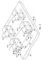
- FIG. 4is a perspective view illustrating an array of silicon pillars formed on a substrate as used in one embodiment according to the teachings of the present invention.
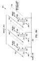
- FIGS. 5A-5Eare cross sectional views taken along cut line 5 - 5 from FIG. 4 illustrating a number of floating gate and control gate configurations which are included in the scope of the present invention.
- FIGS. 6A-6Cillustrate a number of address coincidence schemes can be used together with the present invention.
- FIG. 7Ais an energy band diagram illustrating the band structure at vacuum level with the low tunnel barrier interpoly insulator according to the teachings of the present invention.
- FIG. 7Bis an energy band diagram illustrating the band structure during an erase operation of electrons from the floating gate to the control gate across the low tunnel barrier interpoly insulator according to the teachings of the present invention.
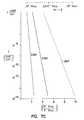
- FIG. 7Cis a graph plotting tunneling currents versus the applied electric fields (reciprocal applied electric field shown) for an number of barrier heights.
- FIG. 8is a schematic diagram illustrating a conventional NOR-NOR programmable logic array.
- FIG. 9is a schematic diagram illustrating generally an architecture of one embodiment of a novel in-service programmable logic array (PLA) with floating gate transistors, or logic cells, according to the teachings of the present invention.
- PLAprogrammable logic array
- FIG. 10is a simplified block diagram of a high-level organization of an electronic system according to the teachings of the present invention.
- wafer and substrateare interchangeably used to refer generally to any structure on which integrated circuits are formed, and also to such structures during various stages of integrated circuit fabrication. Both terms include doped and undoped semiconductors, epitaxial layers of a semiconductor on a supporting semiconductor or insulating material, combinations of such layers, as well as other such structures that are known in the art.
- doped and undoped semiconductorsinclude doped and undoped semiconductors, epitaxial layers of a semiconductor on a supporting semiconductor or insulating material, combinations of such layers, as well as other such structures that are known in the art.
- horizontalas used in this application is defined as a plane parallel to the conventional plane or surface of a wafer or substrate, regardless of the orientation of the wafer or substrate.
- verticalrefers to a direction perpendicular to the horizonal as defined above.
- Prepositions, such as “on”, “side” (as in “sidewall”), “higher”, “lower”, “over” and “under”are defined with respect to the conventional plane or surface being on the top surface of the wafer or substrate, regardless of the orientation of the wafer or substrate.
- the present inventiondescribes the use of metal oxide inter-poly dielectric insulators between the control gate and the floating gate.
- An exampleis shown in FIG. 2 for a planar structure, or horizontal non-volatile memory cell.
- the use of metal oxide films for this purposeoffer a number of advantages including:
- FIG. 2illustrates one embodiment of a floating gate transistor, or non-volatile memory cell 200 , according to the teachings of the present invention.
- the non-volatile memory cell 200includes a first source/drain region 201 and a second source/drain region 203 separated by a channel region 205 in a substrate 206 .
- a floating gate 209opposes the channel region 205 and is separated therefrom by a gate oxide 211 .
- a control gate 213opposes the floating gate 209 .
- the control gate 213is separated from the floating gate 209 by a low tunnel barrier intergate insulator 215 .
- low tunnel barrier intergate insulator 215includes a metal oxide insulator selected from the group consisting of lead oxide (PbO) and aluminum oxide (Al 2 O 3 ).
- the low tunnel barrier intergate insulator 215includes a transition metal oxide and the transition metal oxide is selected from the group consisting of Ta 2 O 5 , TiO 2 , ZrO 2 , and Nb 2 O 5 .
- the low tunnel barrier intergate insulator 215includes a Perovskite oxide tunnel barrier.
- the floating gate 209includes a polysilicon floating gate 209 having a metal layer 216 formed thereon in contact with the low tunnel barrier intergate insulator 215 .
- the control gate 213includes a polysilicon control gate 213 having a metal layer 217 formed thereon in contact with the low tunnel barrier intergate insulator 215 .
- the metal layers, 216 and 217are formed of the same metal material used to form the metal oxide interpoly insulator 215 .
- FIG. 3illustrates another embodiment of a floating gate transistor, or non-volatile memory cell 300 , according to the teachings of the present invention.
- the non-volatile memory cell 300includes a vertical non volatile memory cell 300 .
- the non-volatile memory cell 300has a first source/drain region 301 formed on a substrate 306 .
- a body region 307 including a channel region 305is formed on the first source/drain region 301 .
- a second source/drain region 303is formed on the body region 307 .
- a floating gate 309opposes the channel region 305 and is separated therefrom by a gate oxide 311 .
- a control gate 313opposes the floating gate 309 .
- the control gate 313is separated from the floating gate 309 by a low tunnel barrier intergate insulator 315 .
- the low tunnel barrier intergate insulator 315includes a metal oxide insulator 315 selected from the group consisting of PbO, Al 2 O 3 , Ta 2 O 5 , TiO 2 , ZrO 2 , and Nb 2 O 5 .
- the low tunnel barrier intergate insulator 315includes a Perovskite oxide tunnel barrier.
- the floating gate 309includes a polysilicon floating gate 309 having a metal layer 316 formed thereon in contact with the low tunnel barrier intergate insulator 315 .
- the control gate 313includes a polysilicon control gate 313 having a metal layer 317 formed thereon in contact with the low tunnel barrier intergate insulator 315 .
- the floating gate 309includes a vertical floating gate 309 formed alongside of the body region 307 .
- the control gate 313includes a vertical control gate 313 formed alongside of the vertical floating gate 309 .
- the floating gate 309 and control gate 313 orientation shown in FIG. 3is just one embodiment for a vertical non volatile memory cell 300 , according to the teachings of the present invention.
- the floating gateincludes a horizontally oriented floating gate formed alongside of the body region.
- the control gateincludes a horizontally oriented control gate formed above the horizontally oriented floating gate.
- FIG. 4is a perspective view illustrating an array of silicon pillars 400 - 1 , 400 - 2 , 400 - 3 , . . . , 400 -N, formed on a substrate 406 as used in one embodiment according to the teachings of the present invention.
- the substratescan be (i) conventional p-type bulk silicon or p-type epitaxial layers on p+ wafers, (ii) silicon on insulator formed by conventional SIMOX, wafer bonding and etch back or silicon on sapphire, or (iii) small islands of silicon on insulator utilizing techniques.
- each pillar in the array of silicon pillars 400 - 1 , 400 - 2 , 400 - 3 , . . . , 400 -Nincludes a first source/drain region 401 and a second source/drain region 403 .
- the first and the second source/drain regions, 401 and 403are separated by a body region 407 including channel regions 405 .
- a number of trenches 430separate adjacent pillars in the array of silicon pillars 400 - 1 , 400 - 2 , 400 - 3 , . . . , 400 -N.
- Trenches 430are referenced in connection with the discussion which follows in connection with FIGS. 5A-5E .
- FIGS. 5A-5Eare cross sectional views taken along cut line 5 - 5 from FIG. 4 .
- FIG. 5Aillustrates one such embodiment of the present invention.
- FIG. 5Aillustrates a first source/drain region 501 and second source/drain region 503 for a non-volatile memory cell 500 formed according to the teachings of the present invention.
- the first and second source/drain regions, 501 and 503are contained in a pillar of semiconductor material, and separated by a body region 507 including channel regions 505 .
- FIGS. 5A-5Eare cross sectional views taken along cut line 5 - 5 from FIG. 4 .
- FIG. 5Aillustrates one such embodiment of the present invention.
- FIG. 5Aillustrates a first source/drain region 501 and second source/drain region 503 for a non-volatile memory cell 500 formed according to the teachings of the present invention.
- the first and second source/drain regions, 501 and 503are contained in a pillar of semiconductor
- the first source/drain region 501is integrally connected to a buried sourceline 525 .
- the buried sourceline 525is be formed of semiconductor material which has the same doping type as the first source/drain region 501 .
- the sourceline 525is formed of semiconductor material of the same doping as the first source/drain region 501 , but is more heavily doped than the first source/drain region 501 .
- a pair of floating gates 509 - 1 and 509 - 2are formed in each trench 530 between adjacent pillars which form memory cells 500 - 1 and 500 - 2 .
- Each one of the pair of floating gates, 509 - 1 and 509 - 2respectively opposes the body regions 507 - 1 and 507 - 2 in adjacent pillars 500 - 1 and 500 - 2 on opposing sides of the trench 530 .
- a single control gate 513is shared by the pair of floating gates 509 - 1 and 509 - 2 on opposing sides of the trench 530 .
- the shared single control gate 513can include an integrally formed control gate line.
- an integrally formed control gate line 513can be one of a plurality of control gate lines which are each independently formed in the trench, such as trench 530 , below the top surface of the pillars 500 - 1 and 500 - 2 and between the pair of floating gates 509 - 1 and 509 - 2 .
- each floating gatee.g. 509 - 1 and 509 - 2 , includes a vertically oriented floating gate having a vertical length of less than 100 nanometers.
- a pair of floating gates 509 - 1 and 509 - 2are formed in each trench 530 between adjacent pillars which form memory cells 500 - 1 and 500 - 2 .
- Each one of the pair of floating gates, 509 - 1 and 509 - 2respectively opposes the body regions 507 - 1 and 507 - 2 in adjacent pillars 500 - 1 and 500 - 2 on opposing sides of the trench 530 .
- a plurality of control gate linesare again formed in trenches, e.g. trench 530 , below the top surface of the pillars, 500 - 1 and 500 - 2 , and between the pair of floating gates 509 - 1 and 509 - 2 .
- each trenche.g. 530
- Each one of the pair of control gate lines 513 - 1 and 513 - 2addresses the floating gates, 509 - 1 and 509 - 2 respectively, on opposing sides of the trench 530 .
- the pair of control gate lines, or control gates 513 - 1 and 513 - 2are separated by an insulator layer.
- a pair of floating gates 509 - 1 and 509 - 2are again formed in each trench 530 between adjacent pillars which form memory cells 500 - 1 and 500 - 2 .
- Each one of the pair of floating gates, 509 - 1 and 509 - 2respectively opposes the body regions 507 - 1 and 507 - 2 in adjacent pillars 500 - 1 and 500 - 2 on opposing sides of the trench 530 .
- the plurality of control gate linesare disposed vertically above the floating gates. That is, in one embodiment, the control gate lines are located above the pair of floating gates 509 - 1 and 509 - 2 and not fully beneath the top surface of the pillars 500 - 1 and 500 - 2 . In the embodiment of FIG. 5C , each pair of floating gates, e.g. 509 - 1 and 509 - 2 , in a given trench shares a single control gate line, or control gate 513 .
- a pair of floating gates 509 - 1 and 509 - 2are formed in each trench 530 between adjacent pillars which form memory cells 500 - 1 and 500 - 2 .
- Each one of the pair of floating gates, 509 - 1 and 509 - 2respectively opposes the body regions 507 - 1 and 507 - 2 in adjacent pillars 500 - 1 and 500 - 2 on opposing sides of the trench 530 .
- the plurality of control gate linesare disposed vertically above the floating gates. That is, in one embodiment, the control gate lines are located above the pair of floating gates 509 - 1 and 509 - 2 and not fully beneath the top surface of the pillars 500 - 1 and 500 - 2 . However, in the embodiment of FIG. 5D , each one of the pair of floating gates, e.g. 509 - 1 and 509 - 2 , is addressed by an independent one of the plurality of control lines or control gates, shown in FIG. 5D as 513 - 1 and 513 - 2 .
- a single floating gate 509is formed in each trench 530 between adjacent pillars which form memory cells 500 - 1 and 500 - 2 .
- the single floating gate 509can be either a vertically oriented floating gate 509 or a horizontally oriented floating gate 509 formed by conventional processing techniques, or can be a horizontally oriented floating gate 509 formed by a replacement gate technique.
- the floating gate 509has a vertical length facing the body region 505 of less than 100 nm. In another embodiment, the floating gate 509 has a vertical length facing the body region 505 of less than 50 nm. In one embodiment, as shown in FIG.
- the floating gate 509is shared, respectively, with the body regions 507 - 1 and 507 - 2 , including channel regions 505 - 1 and 505 - 2 , in adjacent pillars 500 - 1 and 500 - 2 located on opposing sides of the trench 530 .
- the control gateincludes a single horizontally oriented control gate line, or control gate 513 formed above the horizontally oriented floating gate 509 .
- the floating gates 509are separated from the control gate lines, or control gates 513 with a low tunnel barrier intergate insulator in accordance with the descriptions given above in connection with FIG. 3 .
- the modifications hereare to use tunneling through the interpoly dielectric to realize flash memory devices.
- the vertical devicesinclude an extra flexibility in that the capacitors, e.g. gate oxide and intergate insulator, are easily fabricated with different areas. This readily allows the use of very high dielectric constant inter-poly dielectric insulators with lower tunneling barriers.
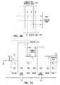
- FIGS. 6A-6Cillustrate that a number of address coincidence schemes can be used together with the present invention.
- FIG. 6Aillustrates a NOR flash memory array 610 having a number of non-volatile memory cells 600 - 1 , 600 - 2 , 600 - 3 , using a coincidence address array scheme.
- FIG. 6Ashows a sourceline 625 coupled to a first source/drain region 601 in each of the number of non-volatile memory cells 600 - 1 , 600 - 2 , 600 - 3 .
- the sourcelineis shown oriented in a first selected direction in the flash memory array 610 .
- FIG. 6Aa number of control gate lines 630 are shown oriented in a second selected direction in the flash memory array 610 .
- the number of control gate lines 630are coupled to, or integrally formed with the control gates 613 for the number of non-volatile memory cells 600 - 1 , 600 - 2 , 600 - 3 .
- the second selected directionis orthogonal to the first selected direction.
- FIG. 6Ashows a number of bitlines 635 oriented in a third selected direction in the flash memory array 610 . As shown in FIG.
- the number of bitlinesare coupled to the second source/drain regions in the number of non-volatile memory cells 600 - 1 , 600 - 2 , 600 - 3 .
- the third selected directionis parallel to the second selected direction and the number of control gate lines 630 serve as address lines.
- the flash memory array 610includes a number of backgate or substrate/well bias address lines 640 coupled to the substrate.
- FIGS. 6B-6Cillustrate of top view for three different coincidence address scheme layouts suitable for use with the present invention.
- FIG. 6Bprovides the top view layout of the coincidence address scheme described in connection with FIG. 6A .
- FIG. 6Billustrates a number of sourcelines 625 oriented in a first selected direction, a number of control gate lines 630 oriented in a second selected direction, and a number of bitlines 635 oriented in a third selected direction for the flash memory array 600 .
- the first selected direction and the third selected directionare parallel to one another and orthogonal to the second selected direction.
- the number of control gate lines 630serve as address lines.
- the output lines, e.g. bitlines 635must be perpendicular to the address lines, e.g. in this embodiment control gate lines 630
- FIG. 6Cprovides the top view layout of yet another coincidence address scheme according to the teachings of the present invention.
- FIG. 6Cillustrates a number of sourcelines 625 oriented in a first selected direction, a number of control gate lines 630 oriented in a second selected direction, and a number of bitlines 635 oriented in a third selected direction for the flash memory array 600 .
- the first selected direction and the second selected directionare parallel to one another and orthogonal to the third selected direction.
- the number of bitlines 635serve as address lines.
- the sourcelines 625can include a uniform ground plane as the same will be known and understood by one of ordinary skill in the art.
- writecan still be achieved by hot electron injection and/or, according to the teachings of the present invention, tunneling from the control gate.
- block eraseis accomplished by driving the control gates with a relatively large positive voltage and tunneling from the metal on top of the floating gate to the metal on the bottom of the control gate.
- FIG. 7Ais an energy band diagram illustrating the band structure at vacuum level with the low tunnel barrier interpoly insulator according to the teachings of the present invention.
- FIG. 7Ais useful in illustrating the reduced tunnel barrier off of the floating gate to the control gate and for illustrating the respective capacitances of the structure according to the teachings of the present invention.
- FIG. 7Ashows the band structure of the silicon substrate, e.g. channel region 701 , silicon dioxide gate insulator, e.g. gate oxide 703 , polysilicon floating gate 705 , the low tunnel barrier interpoly dielectric 707 , between metal plates 709 and 711 , and then the polysilicon control gate 713 , according to the teachings of the present invention.
- the design considerations involvedare determined by the dielectric constant, thickness and tunneling barrier height of the interpoly dielectric insulator 707 relative to that of the silicon dioxide gate insulator, e.g. gate oxide 703 .
- the tunneling probability through the interpoly dielectric 707is an exponential function of both the barrier height and the electric field across this dielectric.
- FIG. 7Bis an energy band diagram illustrating the band structure during an erase operation of electrons from the floating gate 705 to the control gate 713 across the low tunnel barrier interpoly insulator 707 according to the teachings of the present invention.
- FIG. 7Bis similarly useful in illustrating the reduced tunnel barrier off of the floating gate to the control gate and for illustrating the respective capacitances of the structure according to the teachings of the present invention.
- the electric fieldis determined by the total voltage difference across the structure, the ratio of the capacitances (see FIG. 7A ), and the thickness of the interpoly dielectric 707 .
- Ethe electric field across the interpoly dielectric insulator 707 and Eo depends on the barrier height.
- the lower electric field in the aluminum oxide interpoly insulator 707 for the same current densityreflects the lower tunneling barrier of less than 2 eV, shown in FIG. 7B , as opposed to the 3.2 eV tunneling barrier of silicon oxide 703 , also illustrated in FIG. 7B .
- FIG. 7Cis a graph plotting tunneling currents versus the applied electric fields (reciprocal applied electric field shown) for an number of barrier heights.
- FIG. 7Cillustrates the dependence of the tunneling currents on electric field (reciprocal applied electric field) and barrier height.
- the fraction of voltage across the interpoly or intergate insulator, ⁇ V 2can be increased by making the area of the intergate capacitor, C 2 , (e.g. intergate insulator 707 ) smaller than the area of the transistor gate capacitor, C 1 (e.g. gate oxide 703 ). This would be required with high dielectric constant intergate dielectric insulators 707 and is easily realized with the vertical floating gate structures described above in connection with FIGS. 3 , and 5 A- 5 E.
- the poly-Si layeris to be formed with emphasis on obtaining a surface that is very smooth and morphologically stable at subsequent device processing temperatures which will exceed that used to grow Metal oxide.
- the native SiO x oxide on the poly-Si surfacemust be removed (e.g., by sputter cleaning in an inert gas plasma in situ) just prior to depositing the metal film.
- the electrical characteristics of the resultant Poly-Si/Metal/Metal oxide/Metal/Poly-Si structurewill be better defined and reproducible than that of a Poly-Si/Native SiO x /Metal/Metal oxide/Poly-Si structure.
- the oxide growth rate and limiting thicknesswill increase with oxidation temperature and oxygen pressure.
- the oxidation kinetics of a metalmay, in some cases, depend on the crystallographic orientations of the very small grains of metal which comprise the metal film. If such effects are significant, the metal deposition process can be modified in order to increase its preferred orientation and subsequent oxide thickness and tunneling uniformity. To this end, use can be made of the fact that metal films strongly prefer to grow during their depositions having their lowest free energy planes parallel to the film surface. This preference varies with the crystal structure of the metal. For example, fcc metals prefer to form ⁇ 111 ⁇ surface plans. Metal orientation effects, if present, would be larger when only a limited fraction of the metal will be oxidized and unimportant when all or most of the metal is oxidized.
- Modifications in the structure shown in FIG. 2may be introduced in order to compensate for certain properties in some metal/oxide/metal layers. Such changes are reasonable since a wide range of metals, alloys and oxides with quite different physical and chemical properties can be used to form these tunnel junctions.
- Lead and other metal filmscan be deposited by various means including physical sputtering and/or from a Knudsen evaporation cell.
- the sputtering processalso offers the ability to produce smoother films by increasing the re-sputtering-to-deposition ratio since re-sputtering preferentially reduces geometric high points of the film.
- the temperature used to subsequently deposit the Poly-Si control gatemust be held below the melting temperature (327 C) of lead.
- the PbOitself is stable (up to ⁇ 500 C or higher) and thus introduces no temperature constraint on subsequent processes.
- Yet another variation out of severalwould involve: oxidizing the lead film to completion; replacing the top lead electrode with a higher melting metal such as Al; and, then adding the poly-Si control layer. This junction would have asymmetrical tunneling behavior due to the difference in barrier heights between the Pb/PbO and PbO/Al electrodes.
- Tunnel currentsare asymmetrical in this system with somewhat larger currents flowing when electrons are injected from Al/Al 2 O 3 interface developed during oxide growth. This asymmetry is due to a minor change in composition of the growing oxide: there is a small concentration of excess metal in the Al 2 O 3 , the concentration of which diminishes as the oxide is grown thicker. The excess Al +3 ions produce a space charge that lowers the tunnel barrier at the inner interface. The oxide composition at the outer Al 2 O 3 /Al contact is much more stoichiometric and thus has a higher tunnel barrier. In situ ellipsometer measurements on the thermal oxidation of Al films deposited and oxidized in situ support this model.
- Al/Al 2 O 3 /Al tunnel barrierscan be formed that will produce predictable and highly controllable tunnel currents that can be ejected from either electrode.
- the magnitude of the currentsare still primarily dominated by Al 2 O 3 thickness which can be controlled via the oxidation parametrics.
- Al 2 O 3 tunnel barrierswe can proceed to outline one process path out of several that can be used to form Al 2 O 3 tunnel barriers.
- the aluminumis thermally oxidized although one could use other techniques such as plasma oxidation or rf sputtering in an oxygen plasma.
- plasma oxidation or rf sputtering in an oxygen plasmaFor the sake of brevity, some details noted above will not be repeated.
- the formation of the Al/Al 2 O 3 /Al structureswill be seen to be simpler than that described for the Pb/PbO/Pb junctions owing to the much higher melting point of aluminum, relative to lead.
- Single layers of Ta 2 O 5 , TiO 2 , ZrO 2 , Nb 2 O 5 and similar transition metal oxidescan be formed by “low temperature oxidation” of numerous Transition Metal (e.g., TM oxides) films in molecular and plasma oxygen and also by rf sputtering in an oxygen plasma.
- TM oxidesTransition Metal
- the thermal oxidation kinetics of these metalshave been studied for decades. In essence, such metals oxidize via logarithmic kinetics to reach thicknesses of a few to several tens of angstroms in the range of 100 to 300 C.
- Excellent oxide barriers for Josephson tunnel devicescan be formed by rf sputter etching these metals in an oxygen plasma.
- MOCVD filmsrequire high temperature oxidation treatments to remove carbon impurities, improve oxide stoichiometry and produce recrystallization. Such high temperature treatments also cause unwanted interactions between the oxide and the underlying silicon and thus have necessitated the introduction of interfacial barrier layers.
- TM oxidesare very pure and stoichiometric as formed. They do require at least a brief high temperature (est. 700 to 800 C but may be lower) treatment to transform their microstructures from amorphous to crystalline and thus increase their dielectric constants to the desired values (>20 or so). Unlike MOCVD oxides, this treatment can be carried out in an inert gas atmosphere, thus lessening the possibility of inadvertently oxidizing the poly-Si floating gate.
- the dielectric constants of these TM oxidesare substantially greater (>25 to 30 or more) than those of PbO and Al 2 O 3 .
- Duplex layers of these high dielectric constant oxide filmsare easily fabricated with simple tools and also provide improvement in device yields and reliability. Each oxide layer will contain some level of defects but the probability that such defects will overlap is exceedingly small. Effects of such duplex layers were first reported by one J. M. Eldridge of the present authors and are well known to practitioners of the art.
- TM oxide tunnel barrierscan be grown by rf sputtering in an oxygen ambient. Control over oxide thickness and other properties in these studies were all the more remarkable in view of the fact that the oxides were typically grown on thick (e.g., 5,000 A) metals such as Nb and Ta. In such metal-oxide systems, a range of layers and suboxides can also form, each having their own properties. In the present disclosure, control over the properties of the various TM oxides will be even better since we employ very limited (perhaps 10 to 100 A or so) thicknesses of metal and thereby preclude the formation of significant quantities of unwanted, less controllable sub-oxide films.
- Thermodynamic forceswill drive the oxide compositions to their most stable, fully oxidized state, e.g., Nb 2 O 5 , Ta 2 O 5 , etc. As noted above, it will still be necessary to crystallize these duplex oxide layers. Such treatments can be done by RTP and will be shorter than those used on MOCVD and sputter-deposited oxides since the stoichiometry and purity of the “low temperature oxides” need not be adjusted at high temperature.
- Thinner TM layerswill be used in this invention relative to those used to form DRAMs. Unlike DRAMs where leakage must be eliminated, the duplex oxides used here must be thin enough to carry very controlled levels of current flow when subjected to reasonable applied fields and times.
- TM and their oxidesare highly refractory and etchable (e.g., by RIE). Hence they are quite compatible with poly-Si control gate processes and other subsequent steps.
- a stack of oxide filmshaving quite different properties, for example, a stack comprised of a high dielectric constant (k) oxide/a low k oxide/a high k oxide.
- Low temperature oxidationcan be used to form numerous variations of such structures. While most of this disclosure deals with the formation and use of stacks of oxide dielectrics, it is also possible to use “low temperature oxidation” to form other thin film dielectrics such as nitrides, oxynitrides, etc. that could provide additional functions such as being altered by monochromatic light, etc. These will not be discussed further here.
- the parent alloy films that can be converted to a perovskite oxideare typically comprised of metals having widely different chemical reactivities with oxygen and other common gasses.
- Y—Ba—Cu systemreferenced above, Y and Ba are among the most reactive of metals while the reactivity of Cu approaches (albeit distantly) those of other noble metals.
- thin film barrierssuch as Pd, Pt, etc. or their conductive oxides must be added between the Si and the parent metal film to serve as: electrical contact layers; diffusion barriers; and, oxidation stops.
- the Schottky barrier heights of various TM oxides and perovskite oxides in contact with various metalswill help in the design of the tunnel device.
- the barrier heightswill represent that developed during oxide growth at the parent perovskite alloy/perovskite oxide interface.
- barrier heightscannot be predicted ab initio for such a wide class of materials but will have to be developed as the need arises. This information will have to be developed on a system-by-system basis.
- Writecan be achieved by the normal channel hot electron injection and gate current through the silicon oxide to the floating gate. This is done by selecting a particular column by applying a high control gate voltage and applying relatively large drain voltage as is done with conventional ETOX flash memory devices.
- writecan also be accomplished by applying a positive voltage to the substrate or well select line and a large negative voltage to the control gates, electrons will tunnel from the control gate to the floating gate.
- the low tunnel barrierwill provide an easy write operation and the selection of the substrate or well bias will provide selectivity and address only one device.
- eraseis achieved by providing a negative voltage to the substrate or well address line and a large positive voltage to the control gate. This causes electrons to tunnel off of the floating gate on to the control gate.
- a whole rowcan be erased by addressing all the column lines along that row and a block can be erased by addressing multiple row back gate or substrate/well address lines.
- Readis accomplished as in conventional ETOX flash memory devices.
- a column lineis addressed by applying a positive control gate voltage and sensing the current along the data bit or drain row address line.
- FIG. 8shows a conventional NOR-NOR logic array 800 which is programmable at the gate mask level by either fabricating a thin oxide gate transistor, e.g. logic cells 801 - 1 , 801 - 2 , . . . , 801 -N and 803 - 1 , 803 - 2 , . . . , 803 -N, at the intersection of lines in the array or not fabricating a thin oxide gate transistor, e.g. missing thin oxide transistors, 802 - 1 , 802 - 2 , . . . , 802 -N, at such an intersection.
- a thin oxide gate transistore.g. logic cells 801 - 1 , 801 - 2 , . . . , 801 -N and 803 - 1 , 803 - 2 , . . . , 803 -N, at such an intersection.
- NMOS transistors816 and 818 respectively, are used as load devices.
- the conventional logic array shown in FIG. 8includes a first logic plane 810 which receives a number of input signals at input lines 812 .
- first logic plane 810can include inverters to produce the complementary signals when needed in a specific application.
- First logic plane 810includes a number of thin oxide gate transistors, e.g. transistors 801 - 1 , 801 - 2 , . . . , 801 -N.
- the thin oxide gate transistors, 801 - 1 , 801 - 2 , . . . , 801 -N,are located at the intersection of input lines 812 , and interconnect lines 814 .
- this selective fabrication of thin oxide gate transistore.g. transistors 801 - 1 , 801 - 2 , . . .
- 801 -Nis referred to as programming since the logical function implemented by the programmable logic array is entered into the array by the selective arrangement of the thin oxide gate transistors, or logic cells, 801 - 1 , 801 - 2 , . . . , 801 -N, at the intersections of input lines 812 , and interconnect lines 814 in the array.
- each of the interconnect lines 814acts as a NOR gate for the input lines 812 that are connected to the interconnect lines 814 through the thin oxide gate transistors, 801 - 1 , 801 - 2 , . . . , 801 -N, of the array.
- interconnection line 814 Aacts as a NOR gate for the signals on input lines 812 A and 812 B. That is, interconnect line 814 A is maintained at a high potential unless one or more of the thin oxide gate transistors, 801 - 1 , 801 - 2 , . . . , 801 -N, that are coupled to interconnect line 814 A are turned on by a high logic level signal on one of the input lines 812 .
- each thin oxide gate transistore.g. transistors 801 - 1 , 801 - 2 , . . . , 801 -N, conducts which performs the NOR positive logic circuit function
- an inversion of the OR circuit functionresults from inversion of data onto the interconnect lines 814 through the thin oxide gate transistors, 801 - 1 , 801 - 2 , . . . , 801 -N, of the array.
- a second logic plane 824which includes a number of thin oxide gate transistor, e.g. transistors 803 - 1 , 803 - 2 , . . . , 803 -N.
- the thin oxide gate transistors, 803 - 1 , 803 - 2 , . . . , 803 -N,are located at the intersection of interconnect lines 814 , and output lines 820 .
- the logical function of the second logic plane 824is implemented by the selective arrangement of the thin oxide gate transistors, 803 - 1 , 803 - 2 , . . .
- the second logic plane 824is also configured such that the output lines 820 comprise a logical NOR function of the signals from the interconnection lines 814 that are coupled to particular output lines 820 through the thin oxide gate transistors, 803 - 1 , 803 - 2 , . . . , 803 -N, of the second logic plane 824 .
- the incoming signals on each lineare used to drive the gates of transistors in the NOR logic array as the same is known by one of ordinary skill in the art and will be understood by reading this disclosure.
- FIG. 9illustrates an embodiment of a novel in-service programmable logic array (PLA) formed according to the teachings of the present invention.
- PLA 900implements an illustrative logical function using a two level logic approach.
- PLA 900includes first and second logic planes 910 and 922 .
- the logic functionis implemented using NOR-NOR logic.
- first and second logic planes 910 and 922each include an array of, logic cells; non-volatile memory cells, or floating gate driver transistors, 901 - 1 , 901 - 2 , . . . , 901 -N, and 902 - 1 , 902 - 2 , . . .
- the floating gate driver transistors, 901 - 1 , 901 - 2 , . . . , 901 -N, and 902 - 1 , 902 - 2 , . . . , 902 -Nhave their first source/drain regions coupled to source lines or a conductive source plane, as shown and described in more detail in connection with FIGS. 2 and 7C .
- the floating gate driver transistors, 901 - 1 , 901 - 2 , . . . , 901 -N, and 902 - 1 , 902 - 2 , . . . , 902 -Nare shown as n-channel floating gate transistors. However, the invention is not so limited. Also, as shown in FIG. 9 , a number of p-channel metal oxide semiconductor (PMOS) transistors are provided as load device transistors, 916 and 924 respectively, having their source regions coupled to a voltage potential (VDD).
- PMOSp-channel metal oxide semiconductor
- load device transistors, 916 and 924operate in complement to the floating gate driver transistors, 901 - 1 , 901 - 2 , . . . , 901 -N, and 902 - 1 , 902 - 2 , . . . , 902 -N to form load inverters.
- FIG. 9is provided by way of example and not by way of limitation. Specifically, the teachings of the present application are not limited to programmable logic arrays in the NOR-NOR approach. Further, the teachings of the present application are not limited to the specific logical function shown in FIG. 9 . Other logical functions can be implemented in a programmable logic array, with the floating gate driver transistors, 901 - 1 , 901 - 2 , . . . , 901 -N, and 902 - 1 , 902 - 2 , . . . , 902 -N and load device transistors, 916 and 924 respectively, of the present invention, using any one of the various two level logic approaches.
- First logic plane 910receives a number of input signals at input lines 912 .
- no invertersare provided for generating complements of the input signals.
- first logic plane 910can include inverters to produce the complementary signals when needed in a specific application.
- First logic plane 910includes a number of floating gate driver transistors, 901 - 1 , 901 - 2 , . . . , 901 -N, that form an array such as an array of non-volatile memory cells, or flash memory cells.
- the floating gate driver transistors, 901 - 1 , 901 - 2 , . . . , 901 -Nare located at the intersection of input lines 912 , and interconnect lines 914 . Not all of the floating gate driver transistors, 901 - 1 , 901 - 2 , . . . , 901 -N, are operatively conductive in the first logic plane.
- the floating gate driver transistors, 901 - 1 , 901 - 2 , . . . , 901 -Nare selectively programmed, as described in detail below, to respond to the input lines 912 and change the potential of the interconnect lines 914 so as to implement a desired logic function.
- This selective interconnectionis referred to as programming since the logical function implemented by the programmable logic array is entered into the array by the floating gate driver transistors, 901 - 1 , 901 - 2 , . . . , 901 -N, that are used at the intersections of input lines 912 , and interconnect lines 914 in the array.
- each of the interconnect lines 914acts as a NOR gate for the input lines 912 that are connected to the interconnect lines 914 through the floating gate driver transistors, 901 - 1 , 901 - 2 , . . . , 901 -N, of the array 900 .
- interconnection line 914 Aacts as a NOR gate for the signals on input lines 912 A, 912 B and 912 C.
- Programmability of the vertical floating gate driver transistors, 901 - 1 , 901 - 2 , . . . , 901 -Nis achieved by charging the vertical floating gates. When the vertical floating gate is charged, that floating gate driver transistor, 901 - 1 , 901 - 2 , . .
- a floating gate driver transistors, 901 - 1 , 901 - 2 , . . . , 901 -N programmed in an off stateremains in that state until the charge is removed from its vertical floating gate.
- Floating gate driver transistors, 901 - 1 , 901 - 2 , . . . , 901 -N not having a corresponding vertical floating gate chargedoperate in either an on state or an off state, wherein input signals received by the input lines 912 A, 912 B and 912 C determine the applicable state. If any of the input lines 912 A, 912 B and 912 C are turned on by input signals received by the input lines 912 A, 912 B and 912 C, then a ground is provided to load device transistors 916 . The load device transistors 916 are attached to the interconnect lines 914 .
- the load device transistors 916provide a low voltage level when any one of the floating gate driver transistors, 901 - 1 , 901 - 2 , . . . , 901 -N connected to the corresponding interconnect line 914 is activated. This performs the NOR logic circuit function, an inversion of the OR circuit function results from inversion of data onto the interconnect lines 914 through the floating gate driver transistors, 901 - 1 , 901 - 2 , . . . , 901 -N of the array 900 .
- each of the floating gate driver transistors, 901 - 1 , 901 - 2 , . . . , 901 -N described hereinare formed according to the teachings of the present invention as described in detail in connection with FIGS. 2-7C .
- second logic plane 922comprises a second array of floating gate driver transistors, 902 - 1 , 902 - 2 , . . . , 902 -N that are selectively programmed to provide the second level of the two level logic needed to implement a specific logical function.
- the array of floating gate driver transistors, 902 - 1 , 902 - 2 , . . . , 902 -Nis also configured such that the output lines 920 comprise a logical NOR function of the signals from the interconnection lines 914 that are coupled to particular output lines 920 through the floating gate driver transistors, 902 - 1 , 902 - 2 , . . . , 902 -N of the second logic plane 922 .
- Programmability of the vertical floating gate driver transistors, 902 - 1 , 902 - 2 , . . . , 902 -Nis achieved by charging the vertical floating gate. When the vertical floating gate is charged, that floating gate driver transistor, 902 - 1 , 902 - 2 , . . . , 902 -N will remain in an off state until it is reprogrammed. Applying and removing a charge to the vertical floating gates is performed by tunneling charge between the floating gate and control gates of the floating gate driver transistors, 901 - 1 , 901 - 2 , . . . , 901 -N through a low tunnel barrier interpoly, or intergate insulator as described in detail above and in connection with FIGS. 2-7C . A floating gate driver transistors, 902 - 1 , 902 - 2 , . . . , 902 -N programmed in an off state remains in that state until the charge is removed from the vertical floating gate.
- Floating gate driver transistors, 902 - 1 , 902 - 2 , . . . , 902 -N not having a corresponding vertical floating gate chargedoperate in either an on state or an off state, wherein signals received by the interconnect lines 914 determine the applicable state. If any of the interconnect lines 914 are turned on, then a ground is provided to load device transistors 924 by applying a ground potential to the source line or conductive source plane coupled to the transistors first source/drain region as described herein.
- the load device transistors 924are attached to the output lines 920 .
- the load device transistors 924provide a low voltage level when any one of the floating gate driver transistors, 902 - 1 , 902 - 2 , . . .
- the VDD voltage levelis applied to corresponding output lines 920 for second logic plane 922 when a load device transistor 924 is turned on by a clock signal received at the gate of the load device transistors 924 ( ⁇ ).
- a NOR-NOR electrically programmable logic arrayis most easily implemented utilizing the normal PLA array structure.
- Each of the floating gate driver transistors, 902 - 1 , 902 - 2 , . . . , 902 -N described hereinare formed according to the teachings of the present invention as described in detail in connection with FIGS. 2-7C .
- FIG. 9shows the application of the novel, non-volatile floating gate transistors with low tunnel barrier intergate insulators in a logic array.
- a floating gate driver transistors901 - 1 , 901 - 2 , . . . , 901 -N, and 902 - 1 , 902 - 2 , . . . , 902 -N, is programmed with a negative charge on the vertical floating gate it is effectively removed from the array.
- the array logic functionscan be programmed even when the circuit is in the final circuit or in the field and being used in a system.
- the absence or presence of stored charge on the floating gatesis read by addressing the input lines 912 or control gate lines and y-column/sourcelines to form a coincidence in address at a particular floating gate.
- the control gate linewould for instance be driven positive at some voltage of 1.0 Volts and the y-column/sourceline grounded, if the floating gate is not charged with electrons then the transistor would turn on tending to hold the interconnect line on that particular row down indicating the presence of a stored “one” in the cell. If this particular floating gate is charged with stored electrons, the transistor will not turn on and the presence of a stored “zero” indicated in the cell. In this manner, data stored on a particular floating gate can be read.
- the interconnect linescoupled to the second source/drain region for the non-volatile memory cells in the first logic plane, are driven with a higher drain voltage like 2 Volts for 0.1 micron technology and the control gate line is addressed by some nominal voltage in the range of twice this value. Electrons can also be transfered between the floating gate and the control gate through the low tunnel barrier intergate insulator to selectively program the non-volatile memory cells, according to the teachings of the present invention, by the address scheme as described above in connection with FIGS. 6A-6C .
- Erasureis accomplished by driving the control gate line with a large positive voltage and the sourceline and/or backgate or substrate/well address line of the transistor with a negative bias so the total voltage difference is in the order of 3 Volts causing electrons to tunnel off of the floating gates to the control gates.
- Writingcan be performed, as also described above, by either normal channel hot electron injection, or according to the teachings of the present invention, by driving the control gate line with a large negative voltage and the the sourceline and/or backgate or substrate/well address line of the transistor with a positive bias so the total voltage difference is in the order of 3 Volts causing electrons to tunnel off of the control gates to the floating gates.
- datacan be erased in “bit pairs” since both floating gates on each side of a control gate can be erased at the same time.
- This architectureis amenable to block address schemes where sections of the array are erased and reset at the same time.
- the spatial relationship, or orientation of the input lines 912 , interconnect lines 914 , and output lines 920can parallel the spatial relationship, or orientation configurations detailed above for the floating gates and control gates as described in connection with FIGS. 5A-5E
- FIG. 10is a simplified block diagram of a high-level organization of an electronic system 1000 according to the teachings of the present invention.
- the electronic system 1000is a system whose functional elements consist of an arithmetic/logic unit (ALU), e.g. processor 1020 , a control unit 1030 , a memory unit 1040 , or memory device 1040 , and an input/output (I/O) device 1050 .
- ALUarithmetic/logic unit
- processor 1020e.g. processor 1020
- control unit 1030e.g. processor 1020
- memory unit 1040e.g., a control unit 1030
- memory unit 1040e.g., or memory device 1040
- I/Oinput/output
- Such an electronic system 1000will have a native set of instructions that specify operations to be performed on data by the ALU 1020 and other interactions between the ALU 1020 , the memory device 1040 and the I/O devices 1050 .
- the memory devices 1040
- the control unit 1030coordinates all operations of the ALU 1020 , the memory device 1040 and the I/O devices 1050 by continuously cycling through a set of operations that cause instructions to be fetched from the memory device 1040 and executed.
- service programmable logic arrayscan be implemented to perform many of the logic functions performed by these components.
- arbitrary logic functionsmay be realized in the “sum-of-products” form that is well known to one skilled in the art.
- a logic function sum-of-productsmay be implemented using any of the equivalent two-level logic configurations: AND-OR, NAND-NAND, NOR-OR, OR-NOR, AND-NOR, NAND-AND or OR-AND, and using the novel non-volatile memory cells of the present invention.
- the low tunnel barrier interpoly insulators of the present inventionavoid the large barriers to electron tunneling or hot electron injection presented by the silicon oxide-silicon interface, 3.2 eV, which result in slow write and erase speeds even at very high electric fields.
- the present inventionalso avoids the combination of very high electric fields and damage by hot electron collisions in the which oxide result in a number of operational problems like soft erase error, reliability problems of premature oxide breakdown and a limited number of cycles of write and erase.
- the low tunnel barrier interpoly dielectric insulator erase approach, of the present inventionremedies the above mentioned problems of having a rough top surface on the polysilicon floating gate which results in, poor quality interpoly oxides, sharp points, localized high electric fields, premature breakdown and reliability problems.
- any arbitrary combinational logic functioncan be realized in the so-called sum-of-products form.
- a sum of productsmay be implemented by using a two level logic configuration such as the NOR-NOR arrays shown in FIG. 10 , or by a combination of NOR gates and NAND gates.
- a NAND gatecan be realized by a NOR gate with the inputs inverted.
Landscapes
- Physics & Mathematics (AREA)
- Mathematical Physics (AREA)
- Engineering & Computer Science (AREA)
- Computer Hardware Design (AREA)
- Computing Systems (AREA)
- General Engineering & Computer Science (AREA)
- Non-Volatile Memory (AREA)
- Semiconductor Memories (AREA)
Abstract
Description
where E is the electric field across the interpoly
- (i) Insert certain metals at the TM/poly-Si boundaries that will prevent inter-diffusion of the TM and the poly-Si.
- (ii) Completely oxide the TMs. The electrical characteristics of the resulting poly-Si/
TM oxide 1/TM oxide 2/poly-Si structure will be different in the absence of having TM at the oxide/metal interfaces.
- U.S. Pat. No. 6,498,065, “Memory Address Decode Array with vertical transistors;”
- U.S. Pat. No. 5,691,230, “Technique for Producing Small Islands of Silicon on Insulator;”
- U.S. Pat. No. 6,424,001, “Flash Memory with Ultrathin Vertical Body Transistors;”
- S. R. Pollack and C. E. Morris, “Tunneling through gaseous oxidized films of Al2O3,” Trans. AIME, Vol. 233, p. 497, 1965;
- O. Kubaschewski and B. E. Hopkins, “Oxidation of Metals and Alloys,” Butterworth, London, pp. 53-64, 1962;
- J. M. Eldridge and J. Matisoo, “Measurement of tunnel current density in a Meal-Oxide-Metal system as a function of oxide thickness,” Proc. 12th Intern. Conf. On Low Temperature Physics, pp. 427-428, 1971;
- J. M. Eldridge and D. W. Wong, “Growth of thin PbO layers on lead films. I. Experiment,” Surface Science, Vol. 40, pp. 512-530, 1973;
- J. H. Greiner, “Oxidation of lead films by rf sputter etching in an oxygen plasma,” J. Appl. Phys., Vol. 45, No. 1, pp. 32-37, 1974;
- S. M. Sze, Physics of Semiconductor Devices, Wiley, N.Y., pp. 553-556, 1981;
- G. Simmons and A. El-Badry, “Generalized formula for the electric tunnel effect between similar electrodes separated by a thin insulating film,” J. Appl. Phys., Vol. 34, p. 1793, 1963;
- Z. Hurych, “Influence of nonuniform thickness of dielectric layers on capacitance and tunnel circuits,” Solid-State Electronics, Vol. 9, p. 967, 1966;
- S. P. S. Arya and H. P. Singh, “Conduction properties of Al2O3 films,” Thin solid Films, vol. 91, No. 4, pp. 363-374, May, 1982;
- K.-H. Gundlach and J. Holzl, “Logarithmic conductivity of Al-Al2O3-AL tunneling junctions produced by plasma- and by thermal-oxidation,” Surface Science, Vol. 27, pp. 125-141, 1971;
- J. Grimblot and J. M. Eldridge, “I. Interaction of Al films with O2 at low pressures,” J. Electro. Chem. Soc., Vol. 129, No. 10, pp. 2366-2368, 1982;
- J. Grimblot and J. M. Eldridge, “II. Oxidation of Al films,” J. Electro. Chem. Soc., Vol. 129, No. 10, pp. 2369-2372, 1982;
- J. M. Greiner, “Josephson tunneling barriers by rf sputter etching in an oxygen plasma,” J. Appl. Phys., Vol. 42, No. 12, pp. 5151-5155, 1971;
- U.S. Pat. No. 4,412,902, “Method of fabrication of Josephson tunnel junction;”
- H. F. Luan et al., “High quality Ta2O5 gate dielectrics with Tox, eq<10 angstroms,” IEDM Tech Digest, pp. 141-144, 1999;
- U.S. Pat. No. 6,461,931, “Thin dielectric films for DRAM storage capacitors;”
- U.S. Pat. No. 5,350,738, “Method of manufacturing an oxide superconducting film;”
- Y. Shi et al., “Tunneling leakage current in ultrathin (<a4 nm) nitride/oxide stack dielectrics,” IEEE Electron Device Letters, vol. 19, no. 10, pp/388-390, 1998.
Claims (34)
Priority Applications (2)
| Application Number | Priority Date | Filing Date | Title |
|---|---|---|---|
| US11/202,460US7274067B2 (en) | 2001-08-30 | 2005-08-12 | Service programmable logic arrays with low tunnel barrier interpoly insulators |
| US11/619,080US20070105313A1 (en) | 2001-08-30 | 2007-01-02 | In service programmable logic arrays with low tunnel barrier interpoly insulators |
Applications Claiming Priority (3)
| Application Number | Priority Date | Filing Date | Title |
|---|---|---|---|
| US09/945,512US7087954B2 (en) | 2001-08-30 | 2001-08-30 | In service programmable logic arrays with low tunnel barrier interpoly insulators |
| US10/788,810US7074673B2 (en) | 2001-08-30 | 2004-02-27 | Service programmable logic arrays with low tunnel barrier interpoly insulators |
| US11/202,460US7274067B2 (en) | 2001-08-30 | 2005-08-12 | Service programmable logic arrays with low tunnel barrier interpoly insulators |
Related Parent Applications (1)
| Application Number | Title | Priority Date | Filing Date |
|---|---|---|---|
| US10/788,810ContinuationUS7074673B2 (en) | 2001-08-30 | 2004-02-27 | Service programmable logic arrays with low tunnel barrier interpoly insulators |
Related Child Applications (1)
| Application Number | Title | Priority Date | Filing Date |
|---|---|---|---|
| US11/619,080DivisionUS20070105313A1 (en) | 2001-08-30 | 2007-01-02 | In service programmable logic arrays with low tunnel barrier interpoly insulators |
Publications (2)
| Publication Number | Publication Date |
|---|---|
| US20060001049A1 US20060001049A1 (en) | 2006-01-05 |
| US7274067B2true US7274067B2 (en) | 2007-09-25 |
Family
ID=25483198
Family Applications (4)
| Application Number | Title | Priority Date | Filing Date |
|---|---|---|---|
| US09/945,512Expired - Fee RelatedUS7087954B2 (en) | 2001-08-30 | 2001-08-30 | In service programmable logic arrays with low tunnel barrier interpoly insulators |
| US10/788,810Expired - Fee RelatedUS7074673B2 (en) | 2001-08-30 | 2004-02-27 | Service programmable logic arrays with low tunnel barrier interpoly insulators |
| US11/202,460Expired - LifetimeUS7274067B2 (en) | 2001-08-30 | 2005-08-12 | Service programmable logic arrays with low tunnel barrier interpoly insulators |
| US11/619,080AbandonedUS20070105313A1 (en) | 2001-08-30 | 2007-01-02 | In service programmable logic arrays with low tunnel barrier interpoly insulators |
Family Applications Before (2)
| Application Number | Title | Priority Date | Filing Date |
|---|---|---|---|
| US09/945,512Expired - Fee RelatedUS7087954B2 (en) | 2001-08-30 | 2001-08-30 | In service programmable logic arrays with low tunnel barrier interpoly insulators |
| US10/788,810Expired - Fee RelatedUS7074673B2 (en) | 2001-08-30 | 2004-02-27 | Service programmable logic arrays with low tunnel barrier interpoly insulators |
Family Applications After (1)
| Application Number | Title | Priority Date | Filing Date |
|---|---|---|---|
| US11/619,080AbandonedUS20070105313A1 (en) | 2001-08-30 | 2007-01-02 | In service programmable logic arrays with low tunnel barrier interpoly insulators |
Country Status (1)
| Country | Link |
|---|---|
| US (4) | US7087954B2 (en) |
Cited By (35)
| Publication number | Priority date | Publication date | Assignee | Title |
|---|---|---|---|---|
| US7372096B2 (en) | 2001-08-30 | 2008-05-13 | Micron Technology, Inc. | Programmable array logic or memory with p-channel devices and asymmetrical tunnel barriers |
| US7405454B2 (en) | 2003-03-04 | 2008-07-29 | Micron Technology, Inc. | Electronic apparatus with deposited dielectric layers |
| US7410910B2 (en) | 2005-08-31 | 2008-08-12 | Micron Technology, Inc. | Lanthanum aluminum oxynitride dielectric films |
| US7443715B2 (en) | 2001-08-30 | 2008-10-28 | Micron Technology, Inc. | SRAM cells with repressed floating gate memory, low tunnel barrier interpoly insulators |
| US7446368B2 (en) | 2001-08-30 | 2008-11-04 | Micron Technology, Inc. | Deposition of metal oxide and/or low asymmetrical tunnel barrier interpoly insulators |
| US7545674B2 (en) | 2001-08-30 | 2009-06-09 | Micron Technology, Inc. | Flash memory with low tunnel barrier interpoly insulators |
| US7554161B2 (en) | 2002-06-05 | 2009-06-30 | Micron Technology, Inc. | HfAlO3 films for gate dielectrics |
| US7560395B2 (en) | 2005-01-05 | 2009-07-14 | Micron Technology, Inc. | Atomic layer deposited hafnium tantalum oxide dielectrics |
| US7572695B2 (en) | 2005-05-27 | 2009-08-11 | Micron Technology, Inc. | Hafnium titanium oxide films |
| US7575978B2 (en) | 2005-08-04 | 2009-08-18 | Micron Technology, Inc. | Method for making conductive nanoparticle charge storage element |
| US7589029B2 (en) | 2002-05-02 | 2009-09-15 | Micron Technology, Inc. | Atomic layer deposition and conversion |
| US7588988B2 (en) | 2004-08-31 | 2009-09-15 | Micron Technology, Inc. | Method of forming apparatus having oxide films formed using atomic layer deposition |
| US20090237996A1 (en)* | 2008-03-20 | 2009-09-24 | Micron Technology, Inc. | Memory structure having volatile and non-volatile memory portions |
| US20090283816A1 (en)* | 2008-05-15 | 2009-11-19 | Seagate Technology Llc | Band engineered high-k tunnel oxides for non-volatile memory |
| US7625794B2 (en) | 2003-03-31 | 2009-12-01 | Micron Technology, Inc. | Methods of forming zirconium aluminum oxide |
| US7670646B2 (en) | 2002-05-02 | 2010-03-02 | Micron Technology, Inc. | Methods for atomic-layer deposition |
| US7687409B2 (en) | 2005-03-29 | 2010-03-30 | Micron Technology, Inc. | Atomic layer deposited titanium silicon oxide films |
| US7719065B2 (en) | 2004-08-26 | 2010-05-18 | Micron Technology, Inc. | Ruthenium layer for a dielectric layer containing a lanthanide oxide |
| US20100123210A1 (en)* | 2008-11-18 | 2010-05-20 | Seagate Technology Llc | Asymmetric barrier diode |
| US7927948B2 (en) | 2005-07-20 | 2011-04-19 | Micron Technology, Inc. | Devices with nanocrystals and methods of formation |
| US7936583B2 (en) | 2008-10-30 | 2011-05-03 | Seagate Technology Llc | Variable resistive memory punchthrough access method |
| US7936580B2 (en) | 2008-10-20 | 2011-05-03 | Seagate Technology Llc | MRAM diode array and access method |
| US7935619B2 (en) | 2008-11-07 | 2011-05-03 | Seagate Technology Llc | Polarity dependent switch for resistive sense memory |
| US20110149639A1 (en)* | 2008-11-07 | 2011-06-23 | Seagate Technology Llc | Non-Volatile Memory Cell with Multiple Resistive Sense Elements Sharing a Common Switching Device |
| US7974119B2 (en) | 2008-07-10 | 2011-07-05 | Seagate Technology Llc | Transmission gate-based spin-transfer torque memory unit |
| US7989290B2 (en) | 2005-08-04 | 2011-08-02 | Micron Technology, Inc. | Methods for forming rhodium-based charge traps and apparatus including rhodium-based charge traps |
| US8110469B2 (en) | 2005-08-30 | 2012-02-07 | Micron Technology, Inc. | Graded dielectric layers |
| US8158964B2 (en) | 2009-07-13 | 2012-04-17 | Seagate Technology Llc | Schottky diode switch and memory units containing the same |
| US8159856B2 (en) | 2009-07-07 | 2012-04-17 | Seagate Technology Llc | Bipolar select device for resistive sense memory |
| US8203869B2 (en) | 2008-12-02 | 2012-06-19 | Seagate Technology Llc | Bit line charge accumulation sensing for resistive changing memory |
| US8648426B2 (en) | 2010-12-17 | 2014-02-11 | Seagate Technology Llc | Tunneling transistors |
| US9030867B2 (en) | 2008-10-20 | 2015-05-12 | Seagate Technology Llc | Bipolar CMOS select device for resistive sense memory |
| US20150130023A1 (en)* | 2013-11-08 | 2015-05-14 | Taiwan Semiconductor Manufacturing Company, Ltd. | Three dimensional integrated circuit capacitor |
| US9136457B2 (en) | 2006-09-20 | 2015-09-15 | Hypres, Inc. | Double-masking technique for increasing fabrication yield in superconducting electronics |
| US9741920B1 (en) | 2010-01-08 | 2017-08-22 | Hypres, Inc. | System and method for providing multi-conductive layer metallic interconnects for superconducting integrated circuits |
Families Citing this family (36)
| Publication number | Priority date | Publication date | Assignee | Title |
|---|---|---|---|---|
| US8253183B2 (en) | 2001-06-28 | 2012-08-28 | Samsung Electronics Co., Ltd. | Charge trapping nonvolatile memory devices with a high-K blocking insulation layer |
| DE10228768A1 (en)* | 2001-06-28 | 2003-01-16 | Samsung Electronics Co Ltd | Non-volatile floating trap storage device comprises a semiconductor substrate, a tunnel insulation layer on the substrate, a charge storage layer, a barrier insulation layer, and a gate electrode |
| US20060180851A1 (en)* | 2001-06-28 | 2006-08-17 | Samsung Electronics Co., Ltd. | Non-volatile memory devices and methods of operating the same |
| US7473959B2 (en)* | 2001-06-28 | 2009-01-06 | Samsung Electronics Co., Ltd. | Non-volatile semiconductor memory devices and methods of fabricating the same |
| US7253467B2 (en)* | 2001-06-28 | 2007-08-07 | Samsung Electronics Co., Ltd. | Non-volatile semiconductor memory devices |
| US7012297B2 (en)* | 2001-08-30 | 2006-03-14 | Micron Technology, Inc. | Scalable flash/NV structures and devices with extended endurance |
| US6754108B2 (en) | 2001-08-30 | 2004-06-22 | Micron Technology, Inc. | DRAM cells with repressed floating gate memory, low tunnel barrier interpoly insulators |
| US6778441B2 (en)* | 2001-08-30 | 2004-08-17 | Micron Technology, Inc. | Integrated circuit memory device and method |
| US7087954B2 (en)* | 2001-08-30 | 2006-08-08 | Micron Technology, Inc. | In service programmable logic arrays with low tunnel barrier interpoly insulators |
| US7075829B2 (en)* | 2001-08-30 | 2006-07-11 | Micron Technology, Inc. | Programmable memory address and decode circuits with low tunnel barrier interpoly insulators |
| US6784480B2 (en)* | 2002-02-12 | 2004-08-31 | Micron Technology, Inc. | Asymmetric band-gap engineered nonvolatile memory device |
| TW535242B (en)* | 2002-05-30 | 2003-06-01 | Silicon Based Tech Corp | Methods of fabricating a stack-gate non-volatile memory device and its contactless memory arrays |
| US7221586B2 (en) | 2002-07-08 | 2007-05-22 | Micron Technology, Inc. | Memory utilizing oxide nanolaminates |
| JP2005311300A (en)* | 2004-03-26 | 2005-11-04 | Toshiba Corp | Semiconductor memory device and manufacturing method thereof |
| KR100593750B1 (en)* | 2004-11-10 | 2006-06-28 | 삼성전자주식회사 | Cross-point nonvolatile memory device adopting binary metal oxide film as data storage material film and manufacturing method |
| US8330202B2 (en)* | 2005-02-23 | 2012-12-11 | Micron Technology, Inc. | Germanium-silicon-carbide floating gates in memories |
| US7279740B2 (en) | 2005-05-12 | 2007-10-09 | Micron Technology, Inc. | Band-engineered multi-gated non-volatile memory device with enhanced attributes |
| KR100684899B1 (en)* | 2005-05-18 | 2007-02-20 | 삼성전자주식회사 | Nonvolatile memory |
| US7402850B2 (en)* | 2005-06-21 | 2008-07-22 | Micron Technology, Inc. | Back-side trapped non-volatile memory device |
| US7829938B2 (en)* | 2005-07-14 | 2010-11-09 | Micron Technology, Inc. | High density NAND non-volatile memory device |
| US7629641B2 (en)* | 2005-08-31 | 2009-12-08 | Micron Technology, Inc. | Band engineered nano-crystal non-volatile memory device utilizing enhanced gate injection |
| US7429767B2 (en)* | 2005-09-01 | 2008-09-30 | Micron Technology, Inc. | High performance multi-level non-volatile memory device |
| US7605030B2 (en) | 2006-08-31 | 2009-10-20 | Micron Technology, Inc. | Hafnium tantalum oxynitride high-k dielectric and metal gates |
| US8232175B2 (en) | 2006-09-14 | 2012-07-31 | Spansion Llc | Damascene metal-insulator-metal (MIM) device with improved scaleability |
| DE102007004687B4 (en)* | 2007-01-25 | 2012-03-01 | Hydraulik-Ring Gmbh | Volume quantity dispensing unit and method for calibrating the pressure output signal volume quantity characteristic |
| JP2008205191A (en)* | 2007-02-20 | 2008-09-04 | Toshiba Corp | Nonvolatile semiconductor memory device and nonvolatile semiconductor memory device |
| US8097912B2 (en)* | 2007-06-13 | 2012-01-17 | Macronix International Co. Ltd. | Systems and methods for self convergence during erase of a non-volatile memory device |
| KR101338158B1 (en)* | 2007-07-16 | 2013-12-06 | 삼성전자주식회사 | Non-volatile memory devices and methods of forming the same |
| FR2930073B1 (en)* | 2008-04-11 | 2010-09-03 | Centre Nat Rech Scient | METHOD FOR MANUFACTURING COMPLEMENTARY P AND N TYPE MOSFET TRANSISTORS, AND ELECTRONIC DEVICE COMPRISING SUCH TRANSISTORS, AND PROCESSOR COMPRISING AT LEAST ONE SUCH DEVICE. |
| JP5537130B2 (en)* | 2009-11-25 | 2014-07-02 | 株式会社東芝 | Semiconductor memory device |
| JP2013172081A (en)* | 2012-02-22 | 2013-09-02 | Toshiba Corp | Nonvolatile semiconductor memory device and method of manufacturing the same |
| US9812448B2 (en)* | 2014-12-17 | 2017-11-07 | Samsung Electronics Co., Ltd. | Semiconductor devices and methods for fabricating the same |
| JP7154136B2 (en) | 2017-02-07 | 2022-10-17 | 株式会社半導体エネルギー研究所 | Manufacturing method of semiconductor device |
| CN107093548B (en)* | 2017-04-20 | 2019-09-03 | 泰科天润半导体科技(北京)有限公司 | The method for preparing SiC base MOS device gate dielectric membrane |
| TWI687874B (en)* | 2018-07-26 | 2020-03-11 | 旺宏電子股份有限公司 | Neural network system and methode for controlling the same |
| FR3091010B1 (en)* | 2018-12-24 | 2020-12-04 | Soitec Silicon On Insulator | SEMICONDUCTOR TYPE STRUCTURE FOR DIGITAL AND RADIO FREQUENCY APPLICATIONS, AND METHOD OF MANUFACTURING SUCH A STRUCTURE |
Citations (136)
| Publication number | Priority date | Publication date | Assignee | Title |
|---|---|---|---|---|
| US4295150A (en) | 1978-10-18 | 1981-10-13 | Itt Industries, Inc. | Storage transistor |
| US4412902A (en) | 1981-06-22 | 1983-11-01 | Nippon Telegraph & Telephone Public Corporation | Method of fabrication of Josephson tunnel junction |
| US4510584A (en) | 1982-12-29 | 1985-04-09 | Mostek Corporation | MOS Random access memory cell with nonvolatile storage |
| US4545035A (en) | 1982-07-20 | 1985-10-01 | Mostek Corporation | Dynamic RAM with nonvolatile shadow memory |
| US4556975A (en) | 1983-02-07 | 1985-12-03 | Westinghouse Electric Corp. | Programmable redundancy circuit |
| US4665417A (en) | 1984-09-27 | 1987-05-12 | International Business Machines Corporation | Non-volatile dynamic random access memory cell |
| US4672240A (en) | 1983-02-07 | 1987-06-09 | Westinghouse Electric Corp. | Programmable redundancy circuit |
| US4688078A (en) | 1982-09-30 | 1987-08-18 | Ning Hseih | Partially relaxable composite dielectric structure |
| US4757360A (en) | 1983-07-06 | 1988-07-12 | Rca Corporation | Floating gate memory device with facing asperities on floating and control gates |
| US4780424A (en) | 1987-09-28 | 1988-10-25 | Intel Corporation | Process for fabricating electrically alterable floating gate memory devices |
| US4939559A (en) | 1981-12-14 | 1990-07-03 | International Business Machines Corporation | Dual electron injector structures using a conductive oxide between injectors |
| US5042011A (en) | 1989-05-22 | 1991-08-20 | Micron Technology, Inc. | Sense amplifier pulldown device with tailored edge input |
| US5057448A (en) | 1988-02-26 | 1991-10-15 | Hitachi, Ltd. | Method of making a semiconductor device having DRAM cells and floating gate memory cells |
| US5071782A (en) | 1990-06-28 | 1991-12-10 | Texas Instruments Incorporated | Vertical memory cell array and method of fabrication |
| US5073519A (en) | 1990-10-31 | 1991-12-17 | Texas Instruments Incorporated | Method of fabricating a vertical FET device with low gate to drain overlap capacitance |
| US5153880A (en) | 1990-03-12 | 1992-10-06 | Xicor, Inc. | Field-programmable redundancy apparatus for memory arrays |
| US5280205A (en) | 1992-04-16 | 1994-01-18 | Micron Technology, Inc. | Fast sense amplifier |
| US5331188A (en) | 1992-02-25 | 1994-07-19 | International Business Machines Corporation | Non-volatile DRAM cell |
| US5350738A (en) | 1991-03-27 | 1994-09-27 | International Superconductivity Technology Center | Method of manufacturing an oxide superconductor film |
| US5353431A (en) | 1991-04-29 | 1994-10-04 | Intel Corporation | Memory address decoder with storage for memory attribute information |
| US5399516A (en) | 1992-03-12 | 1995-03-21 | International Business Machines Corporation | Method of making shadow RAM cell having a shallow trench EEPROM |
| US5418389A (en) | 1992-11-09 | 1995-05-23 | Mitsubishi Chemical Corporation | Field-effect transistor with perovskite oxide channel |
| US5429966A (en) | 1993-07-22 | 1995-07-04 | National Science Council | Method of fabricating a textured tunnel oxide for EEPROM applications |
| US5474947A (en) | 1993-12-27 | 1995-12-12 | Motorola Inc. | Nonvolatile memory process |
| US5488612A (en) | 1993-10-04 | 1996-01-30 | International Business Machines, Corporation | Method and apparatus for field testing field programmable logic arrays |
| US5497494A (en) | 1993-07-23 | 1996-03-05 | International Business Machines Corporation | Method for saving and restoring the state of a CPU executing code in protected mode |
| US5498558A (en) | 1994-05-06 | 1996-03-12 | Lsi Logic Corporation | Integrated circuit structure having floating electrode with discontinuous phase of metal silicide formed on a surface thereof and process for making same |
| US5508544A (en) | 1992-12-14 | 1996-04-16 | Texas Instruments Incorporated | Three dimensional FAMOS memory devices |
| US5600592A (en) | 1993-05-28 | 1997-02-04 | Kabushiki Kaisha Toshiba | Nonvolatile semiconductor memory device having a word line to which a negative voltage is applied |
| US5619642A (en) | 1994-12-23 | 1997-04-08 | Emc Corporation | Fault tolerant memory system which utilizes data from a shadow memory device upon the detection of erroneous data in a main memory device |
| US5618761A (en) | 1994-09-16 | 1997-04-08 | Kabushiki Kaisha Toshiba | Method of manufacturing a perovskite thin film dielectric |
| US5618575A (en) | 1992-07-02 | 1997-04-08 | Balzers Aktiengesellschaft | Process and apparatus for the production of a metal oxide layer |
| US5619051A (en) | 1994-06-27 | 1997-04-08 | Nec Corporation | Semiconductor nonvolatile memory cell |
| US5627785A (en) | 1996-03-15 | 1997-05-06 | Micron Technology, Inc. | Memory device with a sense amplifier |
| US5677867A (en) | 1991-06-12 | 1997-10-14 | Hazani; Emanuel | Memory with isolatable expandable bit lines |
| US5691209A (en) | 1995-09-14 | 1997-11-25 | Liberkowski; Janusz B. | Lattice interconnect method and apparatus for manufacturing multi-chip modules |
| US5691230A (en) | 1996-09-04 | 1997-11-25 | Micron Technology, Inc. | Technique for producing small islands of silicon on insulator |
| US5739544A (en) | 1993-05-26 | 1998-04-14 | Matsushita Electric Industrial Co., Ltd. | Quantization functional device utilizing a resonance tunneling effect and method for producing the same |
| US5739567A (en) | 1992-11-02 | 1998-04-14 | Wong; Chun Chiu D. | Highly compact memory device with nonvolatile vertical transistor memory cell |
| US5768192A (en) | 1996-07-23 | 1998-06-16 | Saifun Semiconductors, Ltd. | Non-volatile semiconductor memory cell utilizing asymmetrical charge trapping |
| US5798548A (en) | 1995-05-18 | 1998-08-25 | Sanyo Electric Co., Ltd. | Semiconductor device having multiple control gates |
| US5801401A (en) | 1997-01-29 | 1998-09-01 | Micron Technology, Inc. | Flash memory with microcrystalline silicon carbide film floating gate |
| US5808943A (en) | 1993-12-28 | 1998-09-15 | Nippon Steel Corporation | Semiconductor memory and method of manufacturing the same |
| US5852306A (en) | 1997-01-29 | 1998-12-22 | Micron Technology, Inc. | Flash memory with nanocrystalline silicon film floating gate |
| US5880991A (en) | 1997-04-14 | 1999-03-09 | International Business Machines Corporation | Structure for low cost mixed memory integration, new NVRAM structure, and process for forming the mixed memory and NVRAM structure |
| US5923056A (en) | 1996-10-10 | 1999-07-13 | Lucent Technologies Inc. | Electronic components with doped metal oxide dielectric materials and a process for making electronic components with doped metal oxide dielectric materials |
| US5936274A (en) | 1997-07-08 | 1999-08-10 | Micron Technology, Inc. | High density flash memory |
| US5952692A (en) | 1996-11-15 | 1999-09-14 | Hitachi, Ltd. | Memory device with improved charge storage barrier structure |
| US5959465A (en) | 1994-12-29 | 1999-09-28 | Stmicroelectronics Ltd. | Fast Nor-Nor PLA operating from a single-phase clock |
| US5969383A (en) | 1997-06-16 | 1999-10-19 | Motorola, Inc. | Split-gate memory device and method for accessing the same |
| US5973355A (en) | 1996-05-24 | 1999-10-26 | Nec Corporation | Nonvolatile semiconductor memory device and manufacturing method of the same |
| US5981350A (en) | 1998-05-29 | 1999-11-09 | Micron Technology, Inc. | Method for forming high capacitance memory cells |
| US5986932A (en) | 1997-06-30 | 1999-11-16 | Cypress Semiconductor Corp. | Non-volatile static random access memory and methods for using same |
| US5991225A (en) | 1998-02-27 | 1999-11-23 | Micron Technology, Inc. | Programmable memory address decode array with vertical transistors |
| US6009011A (en) | 1996-12-27 | 1999-12-28 | Sharp Kabushiki Kaisha | Non-volatile memory and method for operating the same |
| US6025627A (en) | 1998-05-29 | 2000-02-15 | Micron Technology, Inc. | Alternate method and structure for improved floating gate tunneling devices |
| US6025228A (en) | 1997-11-25 | 2000-02-15 | Advanced Micro Devices, Inc. | Method of fabricating an oxynitride-capped high dielectric constant interpolysilicon dielectric structure for a low voltage non-volatile memory |
| US6031263A (en) | 1997-07-29 | 2000-02-29 | Micron Technology, Inc. | DEAPROM and transistor with gallium nitride or gallium aluminum nitride gate |
| US6069816A (en) | 1997-11-27 | 2000-05-30 | Rohm Co., Ltd. | High-speed responding data storing device for maintaining stored data without power supply |
| US6069380A (en) | 1997-07-25 | 2000-05-30 | Regents Of The University Of Minnesota | Single-electron floating-gate MOS memory |
| US6077745A (en) | 1997-01-22 | 2000-06-20 | International Business Machines Corporation | Self-aligned diffused source vertical transistors with stack capacitors in a 4F-square memory cell array |
| US6087222A (en) | 1998-03-05 | 2000-07-11 | Taiwan Semiconductor Manufacturing Company | Method of manufacture of vertical split gate flash memory device |
| US6091626A (en) | 1997-04-02 | 2000-07-18 | Texas Instruments Incorporated | Low voltage, low power static random access memory cell |
| US6108240A (en) | 1999-02-04 | 2000-08-22 | Tower Semiconductor Ltd. | Implementation of EEPROM using intermediate gate voltage to avoid disturb conditions |
| US6118159A (en)* | 1998-02-26 | 2000-09-12 | Siemens Aktiengesellschaft | Electrically programmable memory cell configuration |
| US6124729A (en) | 1998-02-27 | 2000-09-26 | Micron Technology, Inc. | Field programmable logic arrays with vertical transistors |
| US6127227A (en) | 1999-01-25 | 2000-10-03 | Taiwan Semiconductor Manufacturing Company | Thin ONO thickness control and gradual gate oxidation suppression by b. N.su2 treatment in flash memory |
| US6134175A (en) | 1998-08-04 | 2000-10-17 | Micron Technology, Inc. | Memory address decode array with vertical transistors |
| US6135175A (en) | 1998-10-09 | 2000-10-24 | Denharco, Inc. | Tree harvester provided with a rotatable worktable |
| US6141238A (en) | 1999-08-30 | 2000-10-31 | Micron Technology, Inc. | Dynamic random access memory (DRAM) cells with repressed ferroelectric memory methods of reading same, and apparatuses including same |
| US6141248A (en) | 1999-07-29 | 2000-10-31 | Micron Technology, Inc. | DRAM and SRAM memory cells with repressed memory |
| US6157061A (en) | 1997-08-29 | 2000-12-05 | Nec Corporation | Nonvolatile semiconductor memory device and method of manufacturing the same |
| US6163049A (en) | 1998-10-13 | 2000-12-19 | Advanced Micro Devices, Inc. | Method of forming a composite interpoly gate dielectric |
| US6169306B1 (en) | 1998-07-27 | 2001-01-02 | Advanced Micro Devices, Inc. | Semiconductor devices comprised of one or more epitaxial layers |
| US6191459B1 (en) | 1996-01-08 | 2001-02-20 | Infineon Technologies Ag | Electrically programmable memory cell array, using charge carrier traps and insulation trenches |
| US6204529B1 (en) | 1999-08-27 | 2001-03-20 | Hsing Lan Lung | 8 bit per cell non-volatile semiconductor memory structure utilizing trench technology and dielectric floating gate |
| US6208164B1 (en) | 1998-08-04 | 2001-03-27 | Micron Technology, Inc. | Programmable logic array with vertical transistors |
| US6210999B1 (en) | 1998-12-04 | 2001-04-03 | Advanced Micro Devices, Inc. | Method and test structure for low-temperature integration of high dielectric constant gate dielectrics into self-aligned semiconductor devices |
| US6229175B1 (en) | 1998-03-23 | 2001-05-08 | Oki Electric Industry Co., Ltd. | Nonvolatile memory |
| US6238976B1 (en) | 1997-07-08 | 2001-05-29 | Micron Technology, Inc. | Method for forming high density flash memory |
| US6246606B1 (en) | 1997-11-13 | 2001-06-12 | Micron Technology, Inc. | Memory using insulator traps |
| US6249460B1 (en) | 2000-02-28 | 2001-06-19 | Micron Technology, Inc. | Dynamic flash memory cells with ultrathin tunnel oxides |
| US20010013621A1 (en) | 1999-12-09 | 2001-08-16 | Kazuo Nakazato | Memory Device |
| US6306708B1 (en) | 2000-02-02 | 2001-10-23 | United Microelectronics Corp. | Fabrication method for an electrically erasable programmable read only memory |
| US6317364B1 (en) | 1992-01-14 | 2001-11-13 | Sandisk Corporation | Multi-state memory |
| US20010041250A1 (en) | 2000-03-07 | 2001-11-15 | Werkhoven Christian J. | Graded thin films |
| US6323844B1 (en) | 1997-08-11 | 2001-11-27 | Fu-Kuo Yeh | Cursor controlling device and the method of the same |
| US20010055838A1 (en) | 2000-04-28 | 2001-12-27 | Matrix Semiconductor Inc. | Nonvolatile memory on SOI and compound semiconductor substrates and method of fabrication |
| US6335554B1 (en) | 1999-03-08 | 2002-01-01 | Kabushiki Kaisha Toshiba | Semiconductor Memory |
| US6341084B2 (en) | 2000-05-15 | 2002-01-22 | Nec Corporation | Magnetic random access memory circuit |
| US20020008324A1 (en) | 2000-07-21 | 2002-01-24 | Mitsubishi Denki Kabushiki Kaisha | Semiconductor device and method of manufacturing same |
| US20020024083A1 (en) | 1999-02-26 | 2002-02-28 | Wendell P. Noble | Dram technology compatible non volatile memory cells |
| US20020028541A1 (en) | 2000-08-14 | 2002-03-07 | Lee Thomas H. | Dense arrays and charge storage devices, and methods for making same |
| US6376312B1 (en)* | 2001-03-26 | 2002-04-23 | Advanced Micro Devices, Inc. | Formation of non-volatile memory device comprised of an array of vertical field effect transistor structures |
| US6377070B1 (en) | 2001-02-09 | 2002-04-23 | Micron Technology, Inc. | In-service programmable logic arrays with ultra thin vertical body transistors |
| US6396745B1 (en)* | 2001-02-15 | 2002-05-28 | United Microelectronics Corp. | Vertical two-transistor flash memory |
| US6424001B1 (en) | 2001-02-09 | 2002-07-23 | Micron Technology, Inc. | Flash memory with ultra thin vertical body transistors |
| US20020106536A1 (en) | 2001-02-02 | 2002-08-08 | Jongho Lee | Dielectric layer for semiconductor device and method of manufacturing the same |
| US6433382B1 (en) | 1995-04-06 | 2002-08-13 | Motorola, Inc. | Split-gate vertically oriented EEPROM device and process |
| US20020109158A1 (en) | 2001-02-09 | 2002-08-15 | Leonard Forbes | Dynamic memory based on single electron storage |
| US20020109138A1 (en) | 2001-02-09 | 2002-08-15 | Micron Technology, Inc. | Programmable memory address and decode circuits with ultra thin vertical body transistors |
| US6440801B1 (en) | 1997-01-22 | 2002-08-27 | International Business Machines Corporation | Structure for folded architecture pillar memory cell |
| US20020137250A1 (en) | 2001-03-20 | 2002-09-26 | Bich-Yen Nguyen | High K dielectric film and method for making |
| US20020140022A1 (en) | 2001-03-29 | 2002-10-03 | Taiwan Semiconductor Manufacturing Co., Ltd. | Vertical split gate field effect transistor (fet) device |
| US6461905B1 (en) | 2002-02-22 | 2002-10-08 | Advanced Micro Devices, Inc. | Dummy gate process to reduce the Vss resistance of flash products |
| US6461931B1 (en) | 2000-08-29 | 2002-10-08 | Micron Technology, Inc. | Thin dielectric films for DRAM storage capacitors |
| US6476434B1 (en) | 1997-07-08 | 2002-11-05 | Micron Tecnology, Inc. | 4 F2 folded bit line dram cell structure having buried bit and word lines |
| US6475857B1 (en) | 2001-06-21 | 2002-11-05 | Samsung Electronics Co., Ltd. | Method of making a scalable two transistor memory device |
| US20020176293A1 (en) | 1999-02-26 | 2002-11-28 | Micron Technology, Inc. | DRAM technology compatible processor/memory chips |
| US20020175326A1 (en) | 1992-06-01 | 2002-11-28 | Yale University | Sub-nanoscale electronic devices and processes |
| US6504207B1 (en) | 2000-06-30 | 2003-01-07 | International Business Machines Corporation | Method to create EEPROM memory structures integrated with high performance logic and NVRAM, and operating conditions for the same |
| US6514842B1 (en) | 1999-07-09 | 2003-02-04 | Micron Technology, Inc. | Low resistance gate flash memory |
| US6519176B1 (en) | 2000-09-29 | 2003-02-11 | Intel Corporation | Dual threshold SRAM cell for single-ended sensing |
| US6521943B1 (en) | 1997-03-19 | 2003-02-18 | Hitachi, Ltd. | Semiconductor device having thin electrode layer adjacent gate insulator and method of manufacture |
| US20030042528A1 (en) | 2001-08-30 | 2003-03-06 | Leonard Forbes | Sram cells with repressed floating gate memory, low tunnel barrier interpoly insulators |
| US20030043637A1 (en) | 2001-08-30 | 2003-03-06 | Micron Technology, Inc | Flash memory with low tunnel barrier interpoly insulators |
| US6541280B2 (en) | 2001-03-20 | 2003-04-01 | Motorola, Inc. | High K dielectric film |
| US6586797B2 (en) | 2001-08-30 | 2003-07-01 | Micron Technology, Inc. | Graded composition gate insulators to reduce tunneling barriers in flash memory devices |
| US20030134475A1 (en) | 2000-07-28 | 2003-07-17 | Frank Hofmann | Method for manufacturing a multi-bit memory cell |
| US20030207032A1 (en) | 2002-05-02 | 2003-11-06 | Micron Technology, Inc. | Methods, systems, and apparatus for atomic-layer deposition of aluminum oxides in integrated circuits |
| US20030207540A1 (en) | 2002-05-02 | 2003-11-06 | Micron Technology, Inc. | Atomic layer-deposited laaio3 films for gate dielectrics |
| US6730575B2 (en) | 2001-08-30 | 2004-05-04 | Micron Technology, Inc. | Methods of forming perovskite-type material and capacitor dielectric having perovskite-type crystalline structure |
| US6740928B2 (en) | 1999-06-04 | 2004-05-25 | Matsushita Electric Industrial Co., Ltd. | Semiconductor device |
| US6753568B1 (en) | 1996-11-15 | 2004-06-22 | Hitachi, Ltd. | Memory device |
| US6754108B2 (en) | 2001-08-30 | 2004-06-22 | Micron Technology, Inc. | DRAM cells with repressed floating gate memory, low tunnel barrier interpoly insulators |
| US6778441B2 (en) | 2001-08-30 | 2004-08-17 | Micron Technology, Inc. | Integrated circuit memory device and method |
| US20040207038A1 (en)* | 2001-06-26 | 2004-10-21 | Franz Hofmann | Transistor-arrangement, method for operating a transistor arrangement as a data storage element and method for producing a transistor-arrangement |
| US20050023603A1 (en) | 2001-08-30 | 2005-02-03 | Micron Technology, Inc. | Atomic layer deposition of metal oxide and/or low asymmetrical tunnel barrier interpoly insulators |
| US20050023595A1 (en) | 2001-08-30 | 2005-02-03 | Micron Technology, Inc. | Programmable array logic or memory devices with asymmetrical tunnel barriers |
| US20050023602A1 (en) | 2001-08-30 | 2005-02-03 | Micron Technology, Inc. | Programmable array logic or memory with p-channel devices and asymmetrical tunnel barriers |
| US20050024945A1 (en) | 2001-08-30 | 2005-02-03 | Micron Technology, Inc. | Programmable memory address and decode circuits with low tunnel barrier interpoly insulators |
| US6894944B2 (en) | 2000-02-10 | 2005-05-17 | Renesas Technology Corp. | Semiconductor integrated circuit device |
| US6950340B2 (en) | 2002-02-12 | 2005-09-27 | Micron Technology, Inc. | Asymmetric band-gap engineered nonvolatile memory device |
| US7074673B2 (en) | 2001-08-30 | 2006-07-11 | Micron Technology, Inc. | Service programmable logic arrays with low tunnel barrier interpoly insulators |
| US20060186458A1 (en) | 2005-02-23 | 2006-08-24 | Micron Technology,Inc. | Germanium-silicon-carbide floating gates in memories |
| US7112841B2 (en) | 2001-08-30 | 2006-09-26 | Micron Technology, Inc. | Graded composition metal oxide tunnel barrier interpoly insulators |
Family Cites Families (13)
| Publication number | Priority date | Publication date | Assignee | Title |
|---|---|---|---|---|
| JPH0567791A (en)* | 1991-06-20 | 1993-03-19 | Mitsubishi Electric Corp | Electrically writable and erasable semiconductor memory device and its manufacture |
| US5315142A (en)* | 1992-03-23 | 1994-05-24 | International Business Machines Corporation | High performance trench EEPROM cell |
| US5705415A (en)* | 1994-10-04 | 1998-01-06 | Motorola, Inc. | Process for forming an electrically programmable read-only memory cell |
| US5751038A (en)* | 1996-11-26 | 1998-05-12 | Philips Electronics North America Corporation | Electrically erasable and programmable read only memory (EEPROM) having multiple overlapping metallization layers |
| US6093606A (en)* | 1998-03-05 | 2000-07-25 | Taiwan Semiconductor Manufacturing Company | Method of manufacture of vertical stacked gate flash memory device |
| US6180461B1 (en)* | 1998-08-03 | 2001-01-30 | Halo Lsi Design & Device Technology, Inc. | Double sidewall short channel split gate flash memory |
| US5950340A (en)* | 1999-02-02 | 1999-09-14 | Woo; Fay Kan-Kyone | Sign box |
| JP2000348493A (en)* | 1999-06-03 | 2000-12-15 | Fujitsu Ltd | Non-volatile memory circuit |
| TW419822B (en)* | 1999-07-12 | 2001-01-21 | Mosel Vitelic Inc | Trench type non-volatile memory cell and its manufacturing method |
| KR100442090B1 (en)* | 2002-03-28 | 2004-07-27 | 삼성전자주식회사 | Non-volatile memory cells having a split gate structure and methods of fabricating the same |
| US7163863B2 (en)* | 2004-06-29 | 2007-01-16 | Skymedi Corporation | Vertical memory cell and manufacturing method thereof |
| US7205601B2 (en)* | 2005-06-09 | 2007-04-17 | Taiwan Semiconductor Manufacturing Company, Ltd. | FinFET split gate EEPROM structure and method of its fabrication |
| US20070018214A1 (en)* | 2005-07-25 | 2007-01-25 | Micron Technology, Inc. | Magnesium titanium oxide films |
- 2001
- 2001-08-30USUS09/945,512patent/US7087954B2/ennot_activeExpired - Fee Related
- 2004
- 2004-02-27USUS10/788,810patent/US7074673B2/ennot_activeExpired - Fee Related
- 2005
- 2005-08-12USUS11/202,460patent/US7274067B2/ennot_activeExpired - Lifetime
- 2007
- 2007-01-02USUS11/619,080patent/US20070105313A1/ennot_activeAbandoned
Patent Citations (172)
| Publication number | Priority date | Publication date | Assignee | Title |
|---|---|---|---|---|
| US4295150A (en) | 1978-10-18 | 1981-10-13 | Itt Industries, Inc. | Storage transistor |
| US4412902A (en) | 1981-06-22 | 1983-11-01 | Nippon Telegraph & Telephone Public Corporation | Method of fabrication of Josephson tunnel junction |
| US4939559A (en) | 1981-12-14 | 1990-07-03 | International Business Machines Corporation | Dual electron injector structures using a conductive oxide between injectors |
| US4545035A (en) | 1982-07-20 | 1985-10-01 | Mostek Corporation | Dynamic RAM with nonvolatile shadow memory |
| US4688078A (en) | 1982-09-30 | 1987-08-18 | Ning Hseih | Partially relaxable composite dielectric structure |
| US4510584A (en) | 1982-12-29 | 1985-04-09 | Mostek Corporation | MOS Random access memory cell with nonvolatile storage |
| US4556975A (en) | 1983-02-07 | 1985-12-03 | Westinghouse Electric Corp. | Programmable redundancy circuit |
| US4672240A (en) | 1983-02-07 | 1987-06-09 | Westinghouse Electric Corp. | Programmable redundancy circuit |
| US4757360A (en) | 1983-07-06 | 1988-07-12 | Rca Corporation | Floating gate memory device with facing asperities on floating and control gates |
| US4665417A (en) | 1984-09-27 | 1987-05-12 | International Business Machines Corporation | Non-volatile dynamic random access memory cell |
| US4780424A (en) | 1987-09-28 | 1988-10-25 | Intel Corporation | Process for fabricating electrically alterable floating gate memory devices |
| US5057448A (en) | 1988-02-26 | 1991-10-15 | Hitachi, Ltd. | Method of making a semiconductor device having DRAM cells and floating gate memory cells |
| US5042011A (en) | 1989-05-22 | 1991-08-20 | Micron Technology, Inc. | Sense amplifier pulldown device with tailored edge input |
| US5153880A (en) | 1990-03-12 | 1992-10-06 | Xicor, Inc. | Field-programmable redundancy apparatus for memory arrays |
| US5071782A (en) | 1990-06-28 | 1991-12-10 | Texas Instruments Incorporated | Vertical memory cell array and method of fabrication |
| US5073519A (en) | 1990-10-31 | 1991-12-17 | Texas Instruments Incorporated | Method of fabricating a vertical FET device with low gate to drain overlap capacitance |
| US5350738A (en) | 1991-03-27 | 1994-09-27 | International Superconductivity Technology Center | Method of manufacturing an oxide superconductor film |
| US5353431A (en) | 1991-04-29 | 1994-10-04 | Intel Corporation | Memory address decoder with storage for memory attribute information |
| US5677867A (en) | 1991-06-12 | 1997-10-14 | Hazani; Emanuel | Memory with isolatable expandable bit lines |
| US6317364B1 (en) | 1992-01-14 | 2001-11-13 | Sandisk Corporation | Multi-state memory |
| US5331188A (en) | 1992-02-25 | 1994-07-19 | International Business Machines Corporation | Non-volatile DRAM cell |
| US5399516A (en) | 1992-03-12 | 1995-03-21 | International Business Machines Corporation | Method of making shadow RAM cell having a shallow trench EEPROM |
| US5280205A (en) | 1992-04-16 | 1994-01-18 | Micron Technology, Inc. | Fast sense amplifier |
| US20020175326A1 (en) | 1992-06-01 | 2002-11-28 | Yale University | Sub-nanoscale electronic devices and processes |
| US5618575A (en) | 1992-07-02 | 1997-04-08 | Balzers Aktiengesellschaft | Process and apparatus for the production of a metal oxide layer |
| US5739567A (en) | 1992-11-02 | 1998-04-14 | Wong; Chun Chiu D. | Highly compact memory device with nonvolatile vertical transistor memory cell |
| US5418389A (en) | 1992-11-09 | 1995-05-23 | Mitsubishi Chemical Corporation | Field-effect transistor with perovskite oxide channel |
| US5508544A (en) | 1992-12-14 | 1996-04-16 | Texas Instruments Incorporated | Three dimensional FAMOS memory devices |
| US5739544A (en) | 1993-05-26 | 1998-04-14 | Matsushita Electric Industrial Co., Ltd. | Quantization functional device utilizing a resonance tunneling effect and method for producing the same |
| US5600592A (en) | 1993-05-28 | 1997-02-04 | Kabushiki Kaisha Toshiba | Nonvolatile semiconductor memory device having a word line to which a negative voltage is applied |
| US5429966A (en) | 1993-07-22 | 1995-07-04 | National Science Council | Method of fabricating a textured tunnel oxide for EEPROM applications |
| US5497494A (en) | 1993-07-23 | 1996-03-05 | International Business Machines Corporation | Method for saving and restoring the state of a CPU executing code in protected mode |
| US5488612A (en) | 1993-10-04 | 1996-01-30 | International Business Machines, Corporation | Method and apparatus for field testing field programmable logic arrays |
| US5474947A (en) | 1993-12-27 | 1995-12-12 | Motorola Inc. | Nonvolatile memory process |
| US5808943A (en) | 1993-12-28 | 1998-09-15 | Nippon Steel Corporation | Semiconductor memory and method of manufacturing the same |
| US5498558A (en) | 1994-05-06 | 1996-03-12 | Lsi Logic Corporation | Integrated circuit structure having floating electrode with discontinuous phase of metal silicide formed on a surface thereof and process for making same |
| US5619051A (en) | 1994-06-27 | 1997-04-08 | Nec Corporation | Semiconductor nonvolatile memory cell |
| US5618761A (en) | 1994-09-16 | 1997-04-08 | Kabushiki Kaisha Toshiba | Method of manufacturing a perovskite thin film dielectric |
| US5619642A (en) | 1994-12-23 | 1997-04-08 | Emc Corporation | Fault tolerant memory system which utilizes data from a shadow memory device upon the detection of erroneous data in a main memory device |
| US5959465A (en) | 1994-12-29 | 1999-09-28 | Stmicroelectronics Ltd. | Fast Nor-Nor PLA operating from a single-phase clock |
| US6433382B1 (en) | 1995-04-06 | 2002-08-13 | Motorola, Inc. | Split-gate vertically oriented EEPROM device and process |
| US5798548A (en) | 1995-05-18 | 1998-08-25 | Sanyo Electric Co., Ltd. | Semiconductor device having multiple control gates |
| US5691209A (en) | 1995-09-14 | 1997-11-25 | Liberkowski; Janusz B. | Lattice interconnect method and apparatus for manufacturing multi-chip modules |
| US6191459B1 (en) | 1996-01-08 | 2001-02-20 | Infineon Technologies Ag | Electrically programmable memory cell array, using charge carrier traps and insulation trenches |
| US5627785A (en) | 1996-03-15 | 1997-05-06 | Micron Technology, Inc. | Memory device with a sense amplifier |
| US5973355A (en) | 1996-05-24 | 1999-10-26 | Nec Corporation | Nonvolatile semiconductor memory device and manufacturing method of the same |
| US5768192A (en) | 1996-07-23 | 1998-06-16 | Saifun Semiconductors, Ltd. | Non-volatile semiconductor memory cell utilizing asymmetrical charge trapping |
| US5691230A (en) | 1996-09-04 | 1997-11-25 | Micron Technology, Inc. | Technique for producing small islands of silicon on insulator |
| US5923056A (en) | 1996-10-10 | 1999-07-13 | Lucent Technologies Inc. | Electronic components with doped metal oxide dielectric materials and a process for making electronic components with doped metal oxide dielectric materials |
| US5952692A (en) | 1996-11-15 | 1999-09-14 | Hitachi, Ltd. | Memory device with improved charge storage barrier structure |
| US6753568B1 (en) | 1996-11-15 | 2004-06-22 | Hitachi, Ltd. | Memory device |
| US6009011A (en) | 1996-12-27 | 1999-12-28 | Sharp Kabushiki Kaisha | Non-volatile memory and method for operating the same |
| US6440801B1 (en) | 1997-01-22 | 2002-08-27 | International Business Machines Corporation | Structure for folded architecture pillar memory cell |
| US6077745A (en) | 1997-01-22 | 2000-06-20 | International Business Machines Corporation | Self-aligned diffused source vertical transistors with stack capacitors in a 4F-square memory cell array |
| US5852306A (en) | 1997-01-29 | 1998-12-22 | Micron Technology, Inc. | Flash memory with nanocrystalline silicon film floating gate |
| US5801401A (en) | 1997-01-29 | 1998-09-01 | Micron Technology, Inc. | Flash memory with microcrystalline silicon carbide film floating gate |
| US6521943B1 (en) | 1997-03-19 | 2003-02-18 | Hitachi, Ltd. | Semiconductor device having thin electrode layer adjacent gate insulator and method of manufacture |
| US6091626A (en) | 1997-04-02 | 2000-07-18 | Texas Instruments Incorporated | Low voltage, low power static random access memory cell |
| US5880991A (en) | 1997-04-14 | 1999-03-09 | International Business Machines Corporation | Structure for low cost mixed memory integration, new NVRAM structure, and process for forming the mixed memory and NVRAM structure |
| US5969383A (en) | 1997-06-16 | 1999-10-19 | Motorola, Inc. | Split-gate memory device and method for accessing the same |
| US5986932A (en) | 1997-06-30 | 1999-11-16 | Cypress Semiconductor Corp. | Non-volatile static random access memory and methods for using same |
| US6476434B1 (en) | 1997-07-08 | 2002-11-05 | Micron Tecnology, Inc. | 4 F2 folded bit line dram cell structure having buried bit and word lines |
| US6143636A (en) | 1997-07-08 | 2000-11-07 | Micron Technology, Inc. | High density flash memory |
| US6238976B1 (en) | 1997-07-08 | 2001-05-29 | Micron Technology, Inc. | Method for forming high density flash memory |
| US5936274A (en) | 1997-07-08 | 1999-08-10 | Micron Technology, Inc. | High density flash memory |
| US6069380A (en) | 1997-07-25 | 2000-05-30 | Regents Of The University Of Minnesota | Single-electron floating-gate MOS memory |
| US6307775B1 (en) | 1997-07-29 | 2001-10-23 | Micron Technology, Inc. | Deaprom and transistor with gallium nitride or gallium aluminum nitride gate |
| US6249020B1 (en) | 1997-07-29 | 2001-06-19 | Micron Technology, Inc. | DEAPROM and transistor with gallium nitride or gallium aluminum nitride gate |
| US6031263A (en) | 1997-07-29 | 2000-02-29 | Micron Technology, Inc. | DEAPROM and transistor with gallium nitride or gallium aluminum nitride gate |
| US6323844B1 (en) | 1997-08-11 | 2001-11-27 | Fu-Kuo Yeh | Cursor controlling device and the method of the same |
| US6157061A (en) | 1997-08-29 | 2000-12-05 | Nec Corporation | Nonvolatile semiconductor memory device and method of manufacturing the same |
| US6246606B1 (en) | 1997-11-13 | 2001-06-12 | Micron Technology, Inc. | Memory using insulator traps |
| US6351411B2 (en) | 1997-11-13 | 2002-02-26 | Micron Technology, Inc. | Memory using insulator traps |
| US6025228A (en) | 1997-11-25 | 2000-02-15 | Advanced Micro Devices, Inc. | Method of fabricating an oxynitride-capped high dielectric constant interpolysilicon dielectric structure for a low voltage non-volatile memory |
| US6069816A (en) | 1997-11-27 | 2000-05-30 | Rohm Co., Ltd. | High-speed responding data storing device for maintaining stored data without power supply |
| US6118159A (en)* | 1998-02-26 | 2000-09-12 | Siemens Aktiengesellschaft | Electrically programmable memory cell configuration |
| US5991225A (en) | 1998-02-27 | 1999-11-23 | Micron Technology, Inc. | Programmable memory address decode array with vertical transistors |
| US6153468A (en) | 1998-02-27 | 2000-11-28 | Micron Technololgy, Inc. | Method of forming a logic array for a decoder |
| US6124729A (en) | 1998-02-27 | 2000-09-26 | Micron Technology, Inc. | Field programmable logic arrays with vertical transistors |
| US6087222A (en) | 1998-03-05 | 2000-07-11 | Taiwan Semiconductor Manufacturing Company | Method of manufacture of vertical split gate flash memory device |
| US6229175B1 (en) | 1998-03-23 | 2001-05-08 | Oki Electric Industry Co., Ltd. | Nonvolatile memory |
| US6025627A (en) | 1998-05-29 | 2000-02-15 | Micron Technology, Inc. | Alternate method and structure for improved floating gate tunneling devices |
| US5981350A (en) | 1998-05-29 | 1999-11-09 | Micron Technology, Inc. | Method for forming high capacitance memory cells |
| US6169306B1 (en) | 1998-07-27 | 2001-01-02 | Advanced Micro Devices, Inc. | Semiconductor devices comprised of one or more epitaxial layers |
| US6134175A (en) | 1998-08-04 | 2000-10-17 | Micron Technology, Inc. | Memory address decode array with vertical transistors |
| US6208164B1 (en) | 1998-08-04 | 2001-03-27 | Micron Technology, Inc. | Programmable logic array with vertical transistors |
| US6135175A (en) | 1998-10-09 | 2000-10-24 | Denharco, Inc. | Tree harvester provided with a rotatable worktable |
| US6163049A (en) | 1998-10-13 | 2000-12-19 | Advanced Micro Devices, Inc. | Method of forming a composite interpoly gate dielectric |
| US6210999B1 (en) | 1998-12-04 | 2001-04-03 | Advanced Micro Devices, Inc. | Method and test structure for low-temperature integration of high dielectric constant gate dielectrics into self-aligned semiconductor devices |
| US6127227A (en) | 1999-01-25 | 2000-10-03 | Taiwan Semiconductor Manufacturing Company | Thin ONO thickness control and gradual gate oxidation suppression by b. N.su2 treatment in flash memory |
| US6108240A (en) | 1999-02-04 | 2000-08-22 | Tower Semiconductor Ltd. | Implementation of EEPROM using intermediate gate voltage to avoid disturb conditions |
| US20020176293A1 (en) | 1999-02-26 | 2002-11-28 | Micron Technology, Inc. | DRAM technology compatible processor/memory chips |
| US20020024083A1 (en) | 1999-02-26 | 2002-02-28 | Wendell P. Noble | Dram technology compatible non volatile memory cells |
| US6335554B1 (en) | 1999-03-08 | 2002-01-01 | Kabushiki Kaisha Toshiba | Semiconductor Memory |
| US6740928B2 (en) | 1999-06-04 | 2004-05-25 | Matsushita Electric Industrial Co., Ltd. | Semiconductor device |
| US6514842B1 (en) | 1999-07-09 | 2003-02-04 | Micron Technology, Inc. | Low resistance gate flash memory |
| US6141248A (en) | 1999-07-29 | 2000-10-31 | Micron Technology, Inc. | DRAM and SRAM memory cells with repressed memory |
| US6204529B1 (en) | 1999-08-27 | 2001-03-20 | Hsing Lan Lung | 8 bit per cell non-volatile semiconductor memory structure utilizing trench technology and dielectric floating gate |
| US6141238A (en) | 1999-08-30 | 2000-10-31 | Micron Technology, Inc. | Dynamic random access memory (DRAM) cells with repressed ferroelectric memory methods of reading same, and apparatuses including same |
| US20010013621A1 (en) | 1999-12-09 | 2001-08-16 | Kazuo Nakazato | Memory Device |
| US6574143B2 (en) | 1999-12-09 | 2003-06-03 | Hitachi Europe, Ltd. | Memory device using hot charge carrier converters |
| US6306708B1 (en) | 2000-02-02 | 2001-10-23 | United Microelectronics Corp. | Fabrication method for an electrically erasable programmable read only memory |
| US6894944B2 (en) | 2000-02-10 | 2005-05-17 | Renesas Technology Corp. | Semiconductor integrated circuit device |
| US6249460B1 (en) | 2000-02-28 | 2001-06-19 | Micron Technology, Inc. | Dynamic flash memory cells with ultrathin tunnel oxides |
| US20010041250A1 (en) | 2000-03-07 | 2001-11-15 | Werkhoven Christian J. | Graded thin films |
| US20010055838A1 (en) | 2000-04-28 | 2001-12-27 | Matrix Semiconductor Inc. | Nonvolatile memory on SOI and compound semiconductor substrates and method of fabrication |
| US6341084B2 (en) | 2000-05-15 | 2002-01-22 | Nec Corporation | Magnetic random access memory circuit |
| US6504207B1 (en) | 2000-06-30 | 2003-01-07 | International Business Machines Corporation | Method to create EEPROM memory structures integrated with high performance logic and NVRAM, and operating conditions for the same |
| US20020008324A1 (en) | 2000-07-21 | 2002-01-24 | Mitsubishi Denki Kabushiki Kaisha | Semiconductor device and method of manufacturing same |
| US20030134475A1 (en) | 2000-07-28 | 2003-07-17 | Frank Hofmann | Method for manufacturing a multi-bit memory cell |
| US6881994B2 (en) | 2000-08-14 | 2005-04-19 | Matrix Semiconductor, Inc. | Monolithic three dimensional array of charge storage devices containing a planarized surface |
| US20020028541A1 (en) | 2000-08-14 | 2002-03-07 | Lee Thomas H. | Dense arrays and charge storage devices, and methods for making same |
| US6461931B1 (en) | 2000-08-29 | 2002-10-08 | Micron Technology, Inc. | Thin dielectric films for DRAM storage capacitors |
| US6519176B1 (en) | 2000-09-29 | 2003-02-11 | Intel Corporation | Dual threshold SRAM cell for single-ended sensing |
| US20020106536A1 (en) | 2001-02-02 | 2002-08-08 | Jongho Lee | Dielectric layer for semiconductor device and method of manufacturing the same |
| US20040032773A1 (en) | 2001-02-09 | 2004-02-19 | Micron Technology, Inc. | Programmable memory address and decode circuits with vertical body transistors |
| US20020109138A1 (en) | 2001-02-09 | 2002-08-15 | Micron Technology, Inc. | Programmable memory address and decode circuits with ultra thin vertical body transistors |
| US20020109158A1 (en) | 2001-02-09 | 2002-08-15 | Leonard Forbes | Dynamic memory based on single electron storage |
| US6377070B1 (en) | 2001-02-09 | 2002-04-23 | Micron Technology, Inc. | In-service programmable logic arrays with ultra thin vertical body transistors |
| US6903367B2 (en) | 2001-02-09 | 2005-06-07 | Micron Technology Inc. | Programmable memory address and decode circuits with vertical body transistors |
| US6424001B1 (en) | 2001-02-09 | 2002-07-23 | Micron Technology, Inc. | Flash memory with ultra thin vertical body transistors |
| US6566682B2 (en) | 2001-02-09 | 2003-05-20 | Micron Technology, Inc. | Programmable memory address and decode circuits with ultra thin vertical body transistors |
| US6396745B1 (en)* | 2001-02-15 | 2002-05-28 | United Microelectronics Corp. | Vertical two-transistor flash memory |
| US20020137250A1 (en) | 2001-03-20 | 2002-09-26 | Bich-Yen Nguyen | High K dielectric film and method for making |
| US6541280B2 (en) | 2001-03-20 | 2003-04-01 | Motorola, Inc. | High K dielectric film |
| US6376312B1 (en)* | 2001-03-26 | 2002-04-23 | Advanced Micro Devices, Inc. | Formation of non-volatile memory device comprised of an array of vertical field effect transistor structures |
| US20020140022A1 (en) | 2001-03-29 | 2002-10-03 | Taiwan Semiconductor Manufacturing Co., Ltd. | Vertical split gate field effect transistor (fet) device |
| US6475857B1 (en) | 2001-06-21 | 2002-11-05 | Samsung Electronics Co., Ltd. | Method of making a scalable two transistor memory device |
| US7154138B2 (en) | 2001-06-26 | 2006-12-26 | Infineon Technologies Ag | Transistor-arrangement, method for operating a transistor arrangement as a data storage element and method for producing a transistor-arrangement |
| US20040207038A1 (en)* | 2001-06-26 | 2004-10-21 | Franz Hofmann | Transistor-arrangement, method for operating a transistor arrangement as a data storage element and method for producing a transistor-arrangement |
| US20050023603A1 (en) | 2001-08-30 | 2005-02-03 | Micron Technology, Inc. | Atomic layer deposition of metal oxide and/or low asymmetrical tunnel barrier interpoly insulators |
| US7042043B2 (en) | 2001-08-30 | 2006-05-09 | Micron Technology, Inc. | Programmable array logic or memory devices with asymmetrical tunnel barriers |
| US6754108B2 (en) | 2001-08-30 | 2004-06-22 | Micron Technology, Inc. | DRAM cells with repressed floating gate memory, low tunnel barrier interpoly insulators |
| US6778441B2 (en) | 2001-08-30 | 2004-08-17 | Micron Technology, Inc. | Integrated circuit memory device and method |
| US20040160830A1 (en) | 2001-08-30 | 2004-08-19 | Micron Technology, Inc. | DRAM cells with repressed floating gate memory, low tunnel barrier interpoly insulators |
| US7187587B2 (en) | 2001-08-30 | 2007-03-06 | Micron Technology, Inc. | Programmable memory address and decode circuits with low tunnel barrier interpoly insulators |
| US7166886B2 (en) | 2001-08-30 | 2007-01-23 | Micron Technology, Inc. | DRAM cells with repressed floating gate memory, low tunnel barrier interpoly insulators |
| US20050023595A1 (en) | 2001-08-30 | 2005-02-03 | Micron Technology, Inc. | Programmable array logic or memory devices with asymmetrical tunnel barriers |
| US20050023602A1 (en) | 2001-08-30 | 2005-02-03 | Micron Technology, Inc. | Programmable array logic or memory with p-channel devices and asymmetrical tunnel barriers |
| US20050024945A1 (en) | 2001-08-30 | 2005-02-03 | Micron Technology, Inc. | Programmable memory address and decode circuits with low tunnel barrier interpoly insulators |
| US20050026349A1 (en) | 2001-08-30 | 2005-02-03 | Micron Technology, Inc. | Flash memory with low tunnel barrier interpoly insulators |
| US6586797B2 (en) | 2001-08-30 | 2003-07-01 | Micron Technology, Inc. | Graded composition gate insulators to reduce tunneling barriers in flash memory devices |
| US20030043637A1 (en) | 2001-08-30 | 2003-03-06 | Micron Technology, Inc | Flash memory with low tunnel barrier interpoly insulators |
| US20030042528A1 (en) | 2001-08-30 | 2003-03-06 | Leonard Forbes | Sram cells with repressed floating gate memory, low tunnel barrier interpoly insulators |
| US20050169054A1 (en) | 2001-08-30 | 2005-08-04 | Micron Technology, Inc. | SRAM cells with repressed floating gate memory, low tunnel barrier interpoly insulators |
| US20060278917A1 (en) | 2001-08-30 | 2006-12-14 | Micron Technology, Inc. | Floating gate structures |
| US6952032B2 (en) | 2001-08-30 | 2005-10-04 | Micron Technology, Inc. | Programmable array logic or memory devices with asymmetrical tunnel barriers |
| US6958937B2 (en) | 2001-08-30 | 2005-10-25 | Micron Technology Inc. | DRAM cells with repressed floating gate memory, low tunnel barrier interpoly insulators |
| US6963103B2 (en) | 2001-08-30 | 2005-11-08 | Micron Technology, Inc. | SRAM cells with repressed floating gate memory, low tunnel barrier interpoly insulators |
| US20060002192A1 (en) | 2001-08-30 | 2006-01-05 | Micron Technology | Integrated circuit memory device and method |
| US7027328B2 (en) | 2001-08-30 | 2006-04-11 | Micron Technology, Inc. | Integrated circuit memory device and method |
| US6730575B2 (en) | 2001-08-30 | 2004-05-04 | Micron Technology, Inc. | Methods of forming perovskite-type material and capacitor dielectric having perovskite-type crystalline structure |
| US7068544B2 (en) | 2001-08-30 | 2006-06-27 | Micron Technology, Inc. | Flash memory with low tunnel barrier interpoly insulators |
| US7075829B2 (en) | 2001-08-30 | 2006-07-11 | Micron Technology, Inc. | Programmable memory address and decode circuits with low tunnel barrier interpoly insulators |
| US7074673B2 (en) | 2001-08-30 | 2006-07-11 | Micron Technology, Inc. | Service programmable logic arrays with low tunnel barrier interpoly insulators |
| US7087954B2 (en) | 2001-08-30 | 2006-08-08 | Micron Technology, Inc. | In service programmable logic arrays with low tunnel barrier interpoly insulators |
| US20060274580A1 (en) | 2001-08-30 | 2006-12-07 | Micron Technology, Inc. | DRAM cells with repressed floating gate memory, low tunnel barrier interpoly insulators |
| US20060199338A1 (en) | 2001-08-30 | 2006-09-07 | Micron Technology, Inc. | Atomic layer deposition of metal oxide and/or low asymmetrical tunnel barrier interpoly insulators |
| US7112841B2 (en) | 2001-08-30 | 2006-09-26 | Micron Technology, Inc. | Graded composition metal oxide tunnel barrier interpoly insulators |
| US20060231886A1 (en) | 2001-08-30 | 2006-10-19 | Micron Technology, Inc. | Programmable array logic or memory with p-channel devices and asymmetrical tunnel barriers |
| US20060234450A1 (en) | 2001-08-30 | 2006-10-19 | Micron Technology, Inc. | Programmable array logic or memory with p-channel devices and asymmetrical tunnel barriers |
| US7126183B2 (en) | 2001-08-30 | 2006-10-24 | Micron Technology, Inc. | Programmable array logic or memory with p-channel devices and asymmetrical tunnel barriers |
| US20060237768A1 (en) | 2001-08-30 | 2006-10-26 | Micron Technology, Inc. | Programmable array logic or memory with p-channel devices and asymmetrical tunnel barriers |
| US7132711B2 (en) | 2001-08-30 | 2006-11-07 | Micron Technology, Inc. | Programmable array logic or memory with p-channel devices and asymmetrical tunnel barriers |
| US7135734B2 (en) | 2001-08-30 | 2006-11-14 | Micron Technology, Inc. | Graded composition metal oxide tunnel barrier interpoly insulators |
| US7136302B2 (en) | 2001-08-30 | 2006-11-14 | Micron Technology, Inc. | Integrated circuit memory device and method |
| US20060263981A1 (en) | 2001-08-30 | 2006-11-23 | Micron Technology, Inc. | DRAM cells with repressed floating gate memory, low tunnel barrier interpoly insulators |
| US6950340B2 (en) | 2002-02-12 | 2005-09-27 | Micron Technology, Inc. | Asymmetric band-gap engineered nonvolatile memory device |
| US6461905B1 (en) | 2002-02-22 | 2002-10-08 | Advanced Micro Devices, Inc. | Dummy gate process to reduce the Vss resistance of flash products |
| US20030207032A1 (en) | 2002-05-02 | 2003-11-06 | Micron Technology, Inc. | Methods, systems, and apparatus for atomic-layer deposition of aluminum oxides in integrated circuits |
| US20030207540A1 (en) | 2002-05-02 | 2003-11-06 | Micron Technology, Inc. | Atomic layer-deposited laaio3 films for gate dielectrics |
| US20060186458A1 (en) | 2005-02-23 | 2006-08-24 | Micron Technology,Inc. | Germanium-silicon-carbide floating gates in memories |
Non-Patent Citations (53)
| Title |
|---|
| Aarik, Jaan , et al., "Anomalous effect of temperature on atomic layer deposition of titanium dioxide", Journal of Crystal Growth,220(4) (Dec. 2000), 531-537. |
| Aarik, Jaan , et al., "Texture development in nanocrystalline hafnium dioxide thin films grown by atomic layer deposition", Journal of Crystal Growth, 220(1-2), (Nov. 15, 2000), 105-113. |
| Afanas'ev, V , et al., "Electron energy barriers between (100)Si and ultrathin stacks of SiO2, Al2O3, and ZrO3 and ZrO2 insulators", Applied Physics Letters, 78(20), (May 14, 2001), 3073-3075. |
| Ahn, Kie Y., et al., "Magnesium Titanium Oxide Films", U.S. Appl. No. 11/189,075, filed Jul. 25, 2005. |
| Arya, S. P., et al., "Conduction properties of thin Al/sub 2/O/sub 3/ films", Thin Solid Films, 91(4), (May 28, 1982), 363-374. |
| Dipert, Brian , "Flash Memory Goes Mainstream", IEEE Spectrum, 30(10), (Oct. 1993), 48-52. |
| Eierdal, L. , et al., "Interaction of oxygen with Nl(110) studies by scanning tunneling microscopy", Surface Science, 312(1-2), (Jun. 1994), 31-53. |
| Eitan, Boaz , et al., "NROM: A Novel Localized Trapping, 2-Bit Nonvolatile Memory Cell", IEEE Electron Device Letters, 21(11), (Nov. 2000),543-545. |
| Eldridge, J. , et al., "Measurement of Tunnel Current Density in a Metal-Oxide-Metal System as a Function of Oxide Thickness", Proc. 12th Intern. Conf. on Low Temperature Physics, (1971), 427-428. |
| Eldridge, J. M., et al., "Analysis of ultrathin oxide growth on indium", Thin Solid Films, 12(2), (Oct. 1972), 447-451. |
| Eldridge, J. M., et al., "Growth of Thin PbO Layers on Lead Films. I. Experiment", Surface Science, 40(3), (Dec. 1973), 512-530. |
| Ferguson, J D., et al., "Atomic layer deposition of Al2O3 and SiO2 on BN particles using sequential surface reactions", Applied Surface Science, 162-163, (Aug. 1, 2000), 280-292. |
| Greiner, J. , "Josephson Tunneling Barriers by rf Sputter Etching in an Oxygen Plasma", Journal of Applied Physics, 42(12), (Nov. 1971), 5151-5155. |
| Greiner, J. , "Oxidation of lead films by rf sputter etching in an oxygen plasma", Journal of Applied Physics, 45(1), (Jan. 1974), 32-37. |
| Grimblot, J. , et al., "II. Oxidation of Aluminum Films", Journal of the Electrochemical Society, 129(10), (1982), 2369-2372. |
| Grimblot, Jean , et al., "I. Interaction of Al films with O2 at low pressures", Journal of the Electrochemical Society, 129(10), (1982), 2366-2368. |
| Gundlach, K. , et al., "Logarithmic conductivity of Al-Al/sub 2/O/sub 3/-Al tunneling junctions produced by plasma- and by thermal-oxidation", Surface Science, 27(1), (Aug. 1971), 125-141. |
| Guo, X. , "High Quality Ultra-thin (1.5 nm) High quality ultra-thin (1.5 nm) TiO/sub 2/-Si/sub 3/N/sub 4/ gate dielectric for deep sub-micron CMOS technology", International Electron Devices Meeting 1999, Technical Digest, (1999), 137-140. |
| Hodges, D. A., "Analysis and Design of Digital Integrated Circuits, 2nd Edition", McGraw-Hill Publishing, New York, (1988), 354-357. |
| Hodges, D. A., et al., "Analysis and Design of Digital Integrated Circuits", McGraw-Hill Book Company, 2nd Edition, (1988), 394-396. |
| Hurych, Z. , "Influence of Non-Uniform Thickness of Dielectric Layers on Capacitance and Tunnel Currents", Solid-State Electronics, 9, (1966), 967-979. |
| Itokawa, H , "Determination of Bandgap and Energy Band Alignment for High-Dielectric-Constant Gate Insulators Using High-Resolution X-ray Photoelectron Spectroscopy", Extended Abstracts of the 1999 International Conference on Solid State Devices and Materials, (1999), 158-159. |
| Kim, H. , "Leakage current and electrical breakdown in metal-organic chemical vapor deposited TiO/sub 2/ dielectrics on silicon substrates", Applied Physics Letters, 69(25), (Dec. 16, 1996), 3860-3862. |
| Kim, Yeong K., et al., "Novel capacitor technology for high density stand-alone and embedded DRAMs", International Electron Devices Meeting 2000, Technical Digest. IEDM, (2000), 369-372. |
| Kim, Yong S., et al., "Effect of rapid thermal annealing on the structure and the electrical properties of atomic-layer-deposited Ta2O5 films", Journal of the Korean Physical Society, (Dec. 2000), 975-979. |
| Kubaschewski, O. , et al., "Oxidation of Metals and Alloys", Butterworths, London, (1962), 53-63. |
| Kubaschewski, O. , et al., "Oxidation of Metals and Alloys,", Butterworths, London, Second Edition, (1962), 1-3, 5,6, 8-12, 24, 36-39. |
| Kukli, K. , "Development of Dielectric Properties of Niobium Oxide, Tantalum Oxide, and Aluminum Oxide Based Nanolayered Materials", Journal of the Electrochemical Society, 148(2), (Feb. 2001), F35-F41. |
| Kukli, Kaupo , "Atomic Layer Deposition of Titanium Oxide from Til4 and H2O2", Chemical Vapor Deposition, 6(6), (2000), 303-310. |
| Kukli, Kaupo , et al., "Atomic layer deposition of zirconium oxide from zirconium tetraiodide, water and hydrogen peroxide", Journal of Crystal Growth, 231(1-2), (Sep. 2001), 262-272. |
| Kukli, Kaupo , et al., "Real-time monitoring in atomic layer deposition of TiO/sub 2/ from Til/sub 4/ and H/sub 2/O-H/sub 2/O/sub 2/", Langmuir, 16(21), (Oct. 17, 2000), 8122-8128. |
| Kwo, J. , "Properties of high k gate dielectrics Gd2O3 and Y2O3 for Si", Journal of Applied Physics, 89(7), (2001), 3920-3927. |
| Lee, J. , et al., "Effect of polysilicon gate on the flatband voltage shift and mobility degradation for ALD-Al/sub 2/O/sub 3/ gate dielectric", International Electron Devices Meeting 2000, Technical Digest, IEDM, (2000), 645-648. |
| Luan, H. F., et al., "High Quality Ta2O5 Gate Dielectrics with Tox,eq less than 10A", IEDM Technical Digest. International Electron Devices Meeting, (Dec. 5-8, 1999), 141-143. |
| Ma, Yanjun , et al., "Zirconium oxide based gate dielectrics with equivalent oxide thickness of less than 1.0 nm and performance of submicron MOSFET using a nitride gate replacement process", International Electron Devices Meeting 1999, Technical Digest, (1999), 149-152. |
| Marshalek, R. , et al., "Photoresponse Characteristics of Thin-Film Nickel-Nickel Oxide-Nickel Tunneling Junctions", IEEE Journal of Quantum Electronics, QE-19(4), (1983), 743-754. |
| Masuoka, F. , et al., "A 256K Flash EEPROM using Triple Polysilicon Technology", IEEE International Solid-State Circuits Conference, Digest of Technical Papers, (1985), 168-169. |
| Masuoka, F. , et al., "A New Flash EEPROM Cell using Triple Polysilicon Technology", International Electron Devices Meeting, Technical Digest, San Francisco, CA, (1984), 464-467. |
| Mori, S. , et al., "Reliable CVD Inter-Poly Dielectrics for Advanced E&EEPROM", Symposium on VSLI Technology, Digest of Technical Papers, (1985), 16-17. |
| Muller, H. , "Electrical and Optical Properties of Sputtered In2O3 Films", Physica Status Solidi, 27(2), (1968), 723-731. |
| Paranjpe, Ajit , et al., "Atomic layer deposition of AlOx for thin film head gap applications", Journal of the Electrochemical Society, 148(9), (Sep. 2001), 465-471. |
| Pashley, R. , et al., "Flash Memories: the best of two worlds", IEEE Spectrum, 26(12), (Dec. 1989), 30-33. |
| Pollack, S. , et al., "Tunneling Through Gaseous Oxidized Films of Al2O3", Transactions of the Metallurgical Society of AIME, 233, (1965), 497-501. |
| Qi, Wen-Jie , et al., "MOSCAP and MOSFET characteristics using ZrO/sub 2/gate dielectric deposited directly on Si", International Electron Devices Meeting 1999. Technical Digest, (1999), 145-148. |
| Robertson, J. , "Band offsets of wide-band-gap oxides and implications for future electronic devices", Journal of Vacuum Science & Technology B (Microelectronics and Nanometer Structures), 18(3), (May-Jun. 2000), 1785-1791. |
| Robertson, J. , et al., "Schottky Barrier height of Tantalum oxide, barium strontium titanate, lead titanate, and strontium bismuth tantalate", Applied Physics Letters, 74(8), (Feb. 22, 1999), 1168-1170. |
| Shi, Y. , et al., "Tunneling Leakage Current in Ultrathin (less than 4nm) Nitride/Oxide Stack Dielectrics", IEEE Electron Device Letters, 19(10), (Oct. 1998), pp. 388-390. |
| Simmons, J. , "Generalized Formula for the Electric Tunnel Effect between Similiar Electrodes Separated by a Thin Insulating Film", Journal of Applied Physics, 34(6), (1963), 1793-1803. |
| Smith, Ryan C., et al., "Chemical vapour deposition of the oxides of titanium, zirconium and hafnium for use as high-k materials in microelectronic devices. A carbon-free precursor for the synthesis of hafnium dioxide", Advanced Materials for Optics and Electronics, 10(3-5), (May-Oct. 2000), 105-106. |
| Swalin, R. , "Equilibrium between Phases of Variable Composition", In: Thermodynamics of solids, New York, J. Wiley, 2nd Edition,(1972), 165-180. |
| Sze, S. , "Physics of Semiconductor Devices, Second Edition", John Wiley & Sons, New York, (1981), 553-556. |
| Yan, J. , "Structural and electrical characterization of TiO/sub 2/ grown from titanium tetrakis-isopropoxide (TTIP) and TTIP/H/sub 2/O ambients", Journal of Vacuum Science & Technology B (Microelectronics and Nanometer Structures), 14(3), (May-Jun. 1996), 1706-1711. |
| Zhang, H. , "Atomic layer deposition of high dielectric constant nanolaminates", Journal of The Electrochemical Society, 148(4), (Apr. 2001), F63-F66. |
Cited By (83)
| Publication number | Priority date | Publication date | Assignee | Title |
|---|---|---|---|---|
| US7545674B2 (en) | 2001-08-30 | 2009-06-09 | Micron Technology, Inc. | Flash memory with low tunnel barrier interpoly insulators |
| US7372097B2 (en) | 2001-08-30 | 2008-05-13 | Micron Technology, Inc. | Programmable array logic or memory with p-channel devices and asymmetrical tunnel barriers |
| US7391072B2 (en) | 2001-08-30 | 2008-06-24 | Micron Technology, Inc. | Programmable array logic or memory with p-channel devices and asymmetrical tunnel barriers |
| US7759724B2 (en) | 2001-08-30 | 2010-07-20 | Micron Technology, Inc. | Memory cells having gate structure with multiple gates and multiple materials between the gates |
| US7372096B2 (en) | 2001-08-30 | 2008-05-13 | Micron Technology, Inc. | Programmable array logic or memory with p-channel devices and asymmetrical tunnel barriers |
| US7443715B2 (en) | 2001-08-30 | 2008-10-28 | Micron Technology, Inc. | SRAM cells with repressed floating gate memory, low tunnel barrier interpoly insulators |
| US7446368B2 (en) | 2001-08-30 | 2008-11-04 | Micron Technology, Inc. | Deposition of metal oxide and/or low asymmetrical tunnel barrier interpoly insulators |
| US7465983B2 (en) | 2001-08-30 | 2008-12-16 | Micron Technology, Inc. | Low tunnel barrier insulators |
| US7473956B2 (en) | 2001-08-30 | 2009-01-06 | Micron Technology, Inc. | Atomic layer deposition of metal oxide and/or low assymmetrical tunnel barrier interpoly insulators |
| US7476925B2 (en) | 2001-08-30 | 2009-01-13 | Micron Technology, Inc. | Atomic layer deposition of metal oxide and/or low asymmetrical tunnel barrier interploy insulators |
| US7504687B2 (en) | 2001-08-30 | 2009-03-17 | Micron Technology, Inc. | Atomic layer deposition of metal oxide and/or low asymmetrical tunnel barrier interpoly insulators |
| US7508025B2 (en) | 2001-08-30 | 2009-03-24 | Micron Technology, Inc. | Atomic layer deposition of metal oxide and/or low asymmetrical tunnel barrier interpoly insulators |
| US7589029B2 (en) | 2002-05-02 | 2009-09-15 | Micron Technology, Inc. | Atomic layer deposition and conversion |
| US7670646B2 (en) | 2002-05-02 | 2010-03-02 | Micron Technology, Inc. | Methods for atomic-layer deposition |
| US7554161B2 (en) | 2002-06-05 | 2009-06-30 | Micron Technology, Inc. | HfAlO3 films for gate dielectrics |
| US7405454B2 (en) | 2003-03-04 | 2008-07-29 | Micron Technology, Inc. | Electronic apparatus with deposited dielectric layers |
| US7625794B2 (en) | 2003-03-31 | 2009-12-01 | Micron Technology, Inc. | Methods of forming zirconium aluminum oxide |
| US8558325B2 (en) | 2004-08-26 | 2013-10-15 | Micron Technology, Inc. | Ruthenium for a dielectric containing a lanthanide |
| US8907486B2 (en) | 2004-08-26 | 2014-12-09 | Micron Technology, Inc. | Ruthenium for a dielectric containing a lanthanide |
| US7719065B2 (en) | 2004-08-26 | 2010-05-18 | Micron Technology, Inc. | Ruthenium layer for a dielectric layer containing a lanthanide oxide |
| US8154066B2 (en) | 2004-08-31 | 2012-04-10 | Micron Technology, Inc. | Titanium aluminum oxide films |
| US7588988B2 (en) | 2004-08-31 | 2009-09-15 | Micron Technology, Inc. | Method of forming apparatus having oxide films formed using atomic layer deposition |
| US8541276B2 (en) | 2004-08-31 | 2013-09-24 | Micron Technology, Inc. | Methods of forming an insulating metal oxide |
| US7602030B2 (en) | 2005-01-05 | 2009-10-13 | Micron Technology, Inc. | Hafnium tantalum oxide dielectrics |
| US8524618B2 (en) | 2005-01-05 | 2013-09-03 | Micron Technology, Inc. | Hafnium tantalum oxide dielectrics |
| US8278225B2 (en) | 2005-01-05 | 2012-10-02 | Micron Technology, Inc. | Hafnium tantalum oxide dielectrics |
| US7560395B2 (en) | 2005-01-05 | 2009-07-14 | Micron Technology, Inc. | Atomic layer deposited hafnium tantalum oxide dielectrics |
| US7687409B2 (en) | 2005-03-29 | 2010-03-30 | Micron Technology, Inc. | Atomic layer deposited titanium silicon oxide films |
| US8076249B2 (en) | 2005-03-29 | 2011-12-13 | Micron Technology, Inc. | Structures containing titanium silicon oxide |
| US8399365B2 (en) | 2005-03-29 | 2013-03-19 | Micron Technology, Inc. | Methods of forming titanium silicon oxide |
| US7700989B2 (en) | 2005-05-27 | 2010-04-20 | Micron Technology, Inc. | Hafnium titanium oxide films |
| US7572695B2 (en) | 2005-05-27 | 2009-08-11 | Micron Technology, Inc. | Hafnium titanium oxide films |
| US8921914B2 (en) | 2005-07-20 | 2014-12-30 | Micron Technology, Inc. | Devices with nanocrystals and methods of formation |
| US7927948B2 (en) | 2005-07-20 | 2011-04-19 | Micron Technology, Inc. | Devices with nanocrystals and methods of formation |
| US8288818B2 (en) | 2005-07-20 | 2012-10-16 | Micron Technology, Inc. | Devices with nanocrystals and methods of formation |
| US8501563B2 (en) | 2005-07-20 | 2013-08-06 | Micron Technology, Inc. | Devices with nanocrystals and methods of formation |
| US7989290B2 (en) | 2005-08-04 | 2011-08-02 | Micron Technology, Inc. | Methods for forming rhodium-based charge traps and apparatus including rhodium-based charge traps |
| US8314456B2 (en) | 2005-08-04 | 2012-11-20 | Micron Technology, Inc. | Apparatus including rhodium-based charge traps |
| US7575978B2 (en) | 2005-08-04 | 2009-08-18 | Micron Technology, Inc. | Method for making conductive nanoparticle charge storage element |
| US9496355B2 (en) | 2005-08-04 | 2016-11-15 | Micron Technology, Inc. | Conductive nanoparticles |
| US8110469B2 (en) | 2005-08-30 | 2012-02-07 | Micron Technology, Inc. | Graded dielectric layers |
| US9627501B2 (en) | 2005-08-30 | 2017-04-18 | Micron Technology, Inc. | Graded dielectric structures |
| US8951903B2 (en) | 2005-08-30 | 2015-02-10 | Micron Technology, Inc. | Graded dielectric structures |
| US7531869B2 (en)* | 2005-08-31 | 2009-05-12 | Micron Technology, Inc. | Lanthanum aluminum oxynitride dielectric films |
| US7410910B2 (en) | 2005-08-31 | 2008-08-12 | Micron Technology, Inc. | Lanthanum aluminum oxynitride dielectric films |
| US9136457B2 (en) | 2006-09-20 | 2015-09-15 | Hypres, Inc. | Double-masking technique for increasing fabrication yield in superconducting electronics |
| US9595656B2 (en) | 2006-09-20 | 2017-03-14 | Hypres, Inc. | Double-masking technique for increasing fabrication yield in superconducting electronics |
| US10109673B2 (en) | 2006-09-20 | 2018-10-23 | Hypres, Inc. | Double-masking technique for increasing fabrication yield in superconducting electronics |
| US7898857B2 (en)* | 2008-03-20 | 2011-03-01 | Micron Technology, Inc. | Memory structure having volatile and non-volatile memory portions |
| US20090237996A1 (en)* | 2008-03-20 | 2009-09-24 | Micron Technology, Inc. | Memory structure having volatile and non-volatile memory portions |
| US20090283816A1 (en)* | 2008-05-15 | 2009-11-19 | Seagate Technology Llc | Band engineered high-k tunnel oxides for non-volatile memory |
| US7875923B2 (en) | 2008-05-15 | 2011-01-25 | Seagate Technology Llc | Band engineered high-K tunnel oxides for non-volatile memory |
| US8199563B2 (en) | 2008-07-10 | 2012-06-12 | Seagate Technology Llc | Transmission gate-based spin-transfer torque memory unit |
| US7974119B2 (en) | 2008-07-10 | 2011-07-05 | Seagate Technology Llc | Transmission gate-based spin-transfer torque memory unit |
| US8416615B2 (en) | 2008-07-10 | 2013-04-09 | Seagate Technology Llc | Transmission gate-based spin-transfer torque memory unit |
| US9030867B2 (en) | 2008-10-20 | 2015-05-12 | Seagate Technology Llc | Bipolar CMOS select device for resistive sense memory |
| US7936580B2 (en) | 2008-10-20 | 2011-05-03 | Seagate Technology Llc | MRAM diode array and access method |
| US8514605B2 (en) | 2008-10-20 | 2013-08-20 | Seagate Technology Llc | MRAM diode array and access method |
| US8289746B2 (en) | 2008-10-20 | 2012-10-16 | Seagate Technology Llc | MRAM diode array and access method |
| US8199558B2 (en) | 2008-10-30 | 2012-06-12 | Seagate Technology Llc | Apparatus for variable resistive memory punchthrough access method |
| US7936583B2 (en) | 2008-10-30 | 2011-05-03 | Seagate Technology Llc | Variable resistive memory punchthrough access method |
| US7961497B2 (en) | 2008-10-30 | 2011-06-14 | Seagate Technology Llc | Variable resistive memory punchthrough access method |
| US8098510B2 (en) | 2008-10-30 | 2012-01-17 | Seagate Technology Llc | Variable resistive memory punchthrough access method |
| US8508981B2 (en) | 2008-10-30 | 2013-08-13 | Seagate Technology Llc | Apparatus for variable resistive memory punchthrough access method |
| US8508980B2 (en) | 2008-11-07 | 2013-08-13 | Seagate Technology Llc | Polarity dependent switch for resistive sense memory |
| US20110149639A1 (en)* | 2008-11-07 | 2011-06-23 | Seagate Technology Llc | Non-Volatile Memory Cell with Multiple Resistive Sense Elements Sharing a Common Switching Device |
| US7935619B2 (en) | 2008-11-07 | 2011-05-03 | Seagate Technology Llc | Polarity dependent switch for resistive sense memory |
| US8861244B2 (en) | 2008-11-07 | 2014-10-14 | Seagate Technology Llc | Non-volatile memory cell with multiple resistive sense elements sharing a common switching device |
| US8072014B2 (en) | 2008-11-07 | 2011-12-06 | Seagate Technology Llc | Polarity dependent switch for resistive sense memory |
| US8178864B2 (en) | 2008-11-18 | 2012-05-15 | Seagate Technology Llc | Asymmetric barrier diode |
| US20100123210A1 (en)* | 2008-11-18 | 2010-05-20 | Seagate Technology Llc | Asymmetric barrier diode |
| US8638597B2 (en) | 2008-12-02 | 2014-01-28 | Seagate Technology Llc | Bit line charge accumulation sensing for resistive changing memory |
| US8203869B2 (en) | 2008-12-02 | 2012-06-19 | Seagate Technology Llc | Bit line charge accumulation sensing for resistive changing memory |
| US8159856B2 (en) | 2009-07-07 | 2012-04-17 | Seagate Technology Llc | Bipolar select device for resistive sense memory |
| US8514608B2 (en) | 2009-07-07 | 2013-08-20 | Seagate Technology Llc | Bipolar select device for resistive sense memory |
| US8158964B2 (en) | 2009-07-13 | 2012-04-17 | Seagate Technology Llc | Schottky diode switch and memory units containing the same |
| US8198181B1 (en) | 2009-07-13 | 2012-06-12 | Seagate Technology Llc | Schottky diode switch and memory units containing the same |
| US8288749B2 (en) | 2009-07-13 | 2012-10-16 | Seagate Technology Llc | Schottky diode switch and memory units containing the same |
| US9741920B1 (en) | 2010-01-08 | 2017-08-22 | Hypres, Inc. | System and method for providing multi-conductive layer metallic interconnects for superconducting integrated circuits |
| US10833243B1 (en) | 2010-01-08 | 2020-11-10 | SeeQC Inc. | System and method for providing multi-conductive layer metallic interconnects for superconducting integrated circuits |
| US8648426B2 (en) | 2010-12-17 | 2014-02-11 | Seagate Technology Llc | Tunneling transistors |
| US20150130023A1 (en)* | 2013-11-08 | 2015-05-14 | Taiwan Semiconductor Manufacturing Company, Ltd. | Three dimensional integrated circuit capacitor |
| US9202785B2 (en)* | 2013-11-08 | 2015-12-01 | Taiwan Semiconductor Manufacturing Company, Ltd. | Three dimensional integrated circuit capacitor having vias |
Also Published As
| Publication number | Publication date |
|---|---|
| US20040168145A1 (en) | 2004-08-26 |
| US7087954B2 (en) | 2006-08-08 |
| US7074673B2 (en) | 2006-07-11 |
| US20070105313A1 (en) | 2007-05-10 |
| US20030042532A1 (en) | 2003-03-06 |
| US20060001049A1 (en) | 2006-01-05 |
Similar Documents
| Publication | Publication Date | Title |
|---|---|---|
| US7274067B2 (en) | Service programmable logic arrays with low tunnel barrier interpoly insulators | |
| US7075829B2 (en) | Programmable memory address and decode circuits with low tunnel barrier interpoly insulators | |
| US7112841B2 (en) | Graded composition metal oxide tunnel barrier interpoly insulators | |
| US7545674B2 (en) | Flash memory with low tunnel barrier interpoly insulators | |
| US7759724B2 (en) | Memory cells having gate structure with multiple gates and multiple materials between the gates | |
| US7166886B2 (en) | DRAM cells with repressed floating gate memory, low tunnel barrier interpoly insulators | |
| US7136302B2 (en) | Integrated circuit memory device and method | |
| US6952032B2 (en) | Programmable array logic or memory devices with asymmetrical tunnel barriers | |
| US7132711B2 (en) | Programmable array logic or memory with p-channel devices and asymmetrical tunnel barriers |
Legal Events
| Date | Code | Title | Description |
|---|---|---|---|
| FEPP | Fee payment procedure | Free format text:PAYOR NUMBER ASSIGNED (ORIGINAL EVENT CODE: ASPN); ENTITY STATUS OF PATENT OWNER: LARGE ENTITY | |
| STCF | Information on status: patent grant | Free format text:PATENTED CASE | |
| FPAY | Fee payment | Year of fee payment:4 | |
| FPAY | Fee payment | Year of fee payment:8 | |
| AS | Assignment | Owner name:U.S. BANK NATIONAL ASSOCIATION, AS COLLATERAL AGENT, CALIFORNIA Free format text:SECURITY INTEREST;ASSIGNOR:MICRON TECHNOLOGY, INC.;REEL/FRAME:038669/0001 Effective date:20160426 Owner name:U.S. BANK NATIONAL ASSOCIATION, AS COLLATERAL AGEN Free format text:SECURITY INTEREST;ASSIGNOR:MICRON TECHNOLOGY, INC.;REEL/FRAME:038669/0001 Effective date:20160426 | |
| AS | Assignment | Owner name:MORGAN STANLEY SENIOR FUNDING, INC., AS COLLATERAL AGENT, MARYLAND Free format text:PATENT SECURITY AGREEMENT;ASSIGNOR:MICRON TECHNOLOGY, INC.;REEL/FRAME:038954/0001 Effective date:20160426 Owner name:MORGAN STANLEY SENIOR FUNDING, INC., AS COLLATERAL Free format text:PATENT SECURITY AGREEMENT;ASSIGNOR:MICRON TECHNOLOGY, INC.;REEL/FRAME:038954/0001 Effective date:20160426 | |
| AS | Assignment | Owner name:U.S. BANK NATIONAL ASSOCIATION, AS COLLATERAL AGENT, CALIFORNIA Free format text:CORRECTIVE ASSIGNMENT TO CORRECT THE REPLACE ERRONEOUSLY FILED PATENT #7358718 WITH THE CORRECT PATENT #7358178 PREVIOUSLY RECORDED ON REEL 038669 FRAME 0001. ASSIGNOR(S) HEREBY CONFIRMS THE SECURITY INTEREST;ASSIGNOR:MICRON TECHNOLOGY, INC.;REEL/FRAME:043079/0001 Effective date:20160426 Owner name:U.S. BANK NATIONAL ASSOCIATION, AS COLLATERAL AGEN Free format text:CORRECTIVE ASSIGNMENT TO CORRECT THE REPLACE ERRONEOUSLY FILED PATENT #7358718 WITH THE CORRECT PATENT #7358178 PREVIOUSLY RECORDED ON REEL 038669 FRAME 0001. ASSIGNOR(S) HEREBY CONFIRMS THE SECURITY INTEREST;ASSIGNOR:MICRON TECHNOLOGY, INC.;REEL/FRAME:043079/0001 Effective date:20160426 | |
| AS | Assignment | Owner name:JPMORGAN CHASE BANK, N.A., AS COLLATERAL AGENT, ILLINOIS Free format text:SECURITY INTEREST;ASSIGNORS:MICRON TECHNOLOGY, INC.;MICRON SEMICONDUCTOR PRODUCTS, INC.;REEL/FRAME:047540/0001 Effective date:20180703 Owner name:JPMORGAN CHASE BANK, N.A., AS COLLATERAL AGENT, IL Free format text:SECURITY INTEREST;ASSIGNORS:MICRON TECHNOLOGY, INC.;MICRON SEMICONDUCTOR PRODUCTS, INC.;REEL/FRAME:047540/0001 Effective date:20180703 | |
| AS | Assignment | Owner name:MICRON TECHNOLOGY, INC., IDAHO Free format text:RELEASE BY SECURED PARTY;ASSIGNOR:U.S. BANK NATIONAL ASSOCIATION, AS COLLATERAL AGENT;REEL/FRAME:047243/0001 Effective date:20180629 | |
| MAFP | Maintenance fee payment | Free format text:PAYMENT OF MAINTENANCE FEE, 12TH YEAR, LARGE ENTITY (ORIGINAL EVENT CODE: M1553); ENTITY STATUS OF PATENT OWNER: LARGE ENTITY Year of fee payment:12 | |
| AS | Assignment | Owner name:MICRON TECHNOLOGY, INC., IDAHO Free format text:RELEASE BY SECURED PARTY;ASSIGNOR:MORGAN STANLEY SENIOR FUNDING, INC., AS COLLATERAL AGENT;REEL/FRAME:050937/0001 Effective date:20190731 | |
| AS | Assignment | Owner name:MICRON SEMICONDUCTOR PRODUCTS, INC., IDAHO Free format text:RELEASE BY SECURED PARTY;ASSIGNOR:JPMORGAN CHASE BANK, N.A., AS COLLATERAL AGENT;REEL/FRAME:051028/0001 Effective date:20190731 Owner name:MICRON TECHNOLOGY, INC., IDAHO Free format text:RELEASE BY SECURED PARTY;ASSIGNOR:JPMORGAN CHASE BANK, N.A., AS COLLATERAL AGENT;REEL/FRAME:051028/0001 Effective date:20190731 |