US7273769B1 - Method and apparatus for removing encapsulating material from a packaged microelectronic device - Google Patents
Method and apparatus for removing encapsulating material from a packaged microelectronic deviceDownload PDFInfo
- Publication number
- US7273769B1 US7273769B1US09/639,917US63991700AUS7273769B1US 7273769 B1US7273769 B1US 7273769B1US 63991700 AUS63991700 AUS 63991700AUS 7273769 B1US7273769 B1US 7273769B1
- Authority
- US
- United States
- Prior art keywords
- encapsulating material
- microelectronic substrate
- support member
- directing
- laser beam
- Prior art date
- Legal status (The legal status is an assumption and is not a legal conclusion. Google has not performed a legal analysis and makes no representation as to the accuracy of the status listed.)
- Expired - Lifetime, expires
Links
Images


Classifications
- H—ELECTRICITY
- H01—ELECTRIC ELEMENTS
- H01L—SEMICONDUCTOR DEVICES NOT COVERED BY CLASS H10
- H01L23/00—Details of semiconductor or other solid state devices
- H01L23/48—Arrangements for conducting electric current to or from the solid state body in operation, e.g. leads, terminal arrangements ; Selection of materials therefor
- H01L23/488—Arrangements for conducting electric current to or from the solid state body in operation, e.g. leads, terminal arrangements ; Selection of materials therefor consisting of soldered or bonded constructions
- H01L23/495—Lead-frames or other flat leads
- H01L23/49503—Lead-frames or other flat leads characterised by the die pad
- H01L23/4951—Chip-on-leads or leads-on-chip techniques, i.e. inner lead fingers being used as die pad
- H—ELECTRICITY
- H01—ELECTRIC ELEMENTS
- H01L—SEMICONDUCTOR DEVICES NOT COVERED BY CLASS H10
- H01L21/00—Processes or apparatus adapted for the manufacture or treatment of semiconductor or solid state devices or of parts thereof
- H01L21/02—Manufacture or treatment of semiconductor devices or of parts thereof
- H01L21/04—Manufacture or treatment of semiconductor devices or of parts thereof the devices having potential barriers, e.g. a PN junction, depletion layer or carrier concentration layer
- H01L21/50—Assembly of semiconductor devices using processes or apparatus not provided for in a single one of the groups H01L21/18 - H01L21/326 or H10D48/04 - H10D48/07 e.g. sealing of a cap to a base of a container
- H01L21/56—Encapsulations, e.g. encapsulation layers, coatings
- H01L21/565—Moulds
- H—ELECTRICITY
- H01—ELECTRIC ELEMENTS
- H01L—SEMICONDUCTOR DEVICES NOT COVERED BY CLASS H10
- H01L23/00—Details of semiconductor or other solid state devices
- H01L23/28—Encapsulations, e.g. encapsulating layers, coatings, e.g. for protection
- H01L23/31—Encapsulations, e.g. encapsulating layers, coatings, e.g. for protection characterised by the arrangement or shape
- H01L23/3107—Encapsulations, e.g. encapsulating layers, coatings, e.g. for protection characterised by the arrangement or shape the device being completely enclosed
- H01L23/3114—Encapsulations, e.g. encapsulating layers, coatings, e.g. for protection characterised by the arrangement or shape the device being completely enclosed the device being a chip scale package, e.g. CSP
- H—ELECTRICITY
- H01—ELECTRIC ELEMENTS
- H01L—SEMICONDUCTOR DEVICES NOT COVERED BY CLASS H10
- H01L23/00—Details of semiconductor or other solid state devices
- H01L23/28—Encapsulations, e.g. encapsulating layers, coatings, e.g. for protection
- H01L23/31—Encapsulations, e.g. encapsulating layers, coatings, e.g. for protection characterised by the arrangement or shape
- H01L23/3107—Encapsulations, e.g. encapsulating layers, coatings, e.g. for protection characterised by the arrangement or shape the device being completely enclosed
- H01L23/3121—Encapsulations, e.g. encapsulating layers, coatings, e.g. for protection characterised by the arrangement or shape the device being completely enclosed a substrate forming part of the encapsulation
- H01L23/3128—Encapsulations, e.g. encapsulating layers, coatings, e.g. for protection characterised by the arrangement or shape the device being completely enclosed a substrate forming part of the encapsulation the substrate having spherical bumps for external connection
- H—ELECTRICITY
- H01—ELECTRIC ELEMENTS
- H01L—SEMICONDUCTOR DEVICES NOT COVERED BY CLASS H10
- H01L25/00—Assemblies consisting of a plurality of semiconductor or other solid state devices
- H01L25/03—Assemblies consisting of a plurality of semiconductor or other solid state devices all the devices being of a type provided for in a single subclass of subclasses H10B, H10D, H10F, H10H, H10K or H10N, e.g. assemblies of rectifier diodes
- H01L25/10—Assemblies consisting of a plurality of semiconductor or other solid state devices all the devices being of a type provided for in a single subclass of subclasses H10B, H10D, H10F, H10H, H10K or H10N, e.g. assemblies of rectifier diodes the devices having separate containers
- H01L25/105—Assemblies consisting of a plurality of semiconductor or other solid state devices all the devices being of a type provided for in a single subclass of subclasses H10B, H10D, H10F, H10H, H10K or H10N, e.g. assemblies of rectifier diodes the devices having separate containers the devices being integrated devices of class H10
- H—ELECTRICITY
- H01—ELECTRIC ELEMENTS
- H01L—SEMICONDUCTOR DEVICES NOT COVERED BY CLASS H10
- H01L2224/00—Indexing scheme for arrangements for connecting or disconnecting semiconductor or solid-state bodies and methods related thereto as covered by H01L24/00
- H01L2224/01—Means for bonding being attached to, or being formed on, the surface to be connected, e.g. chip-to-package, die-attach, "first-level" interconnects; Manufacturing methods related thereto
- H01L2224/02—Bonding areas; Manufacturing methods related thereto
- H01L2224/04—Structure, shape, material or disposition of the bonding areas prior to the connecting process
- H01L2224/05—Structure, shape, material or disposition of the bonding areas prior to the connecting process of an individual bonding area
- H01L2224/0554—External layer
- H01L2224/05599—Material
- H—ELECTRICITY
- H01—ELECTRIC ELEMENTS
- H01L—SEMICONDUCTOR DEVICES NOT COVERED BY CLASS H10
- H01L2224/00—Indexing scheme for arrangements for connecting or disconnecting semiconductor or solid-state bodies and methods related thereto as covered by H01L24/00
- H01L2224/01—Means for bonding being attached to, or being formed on, the surface to be connected, e.g. chip-to-package, die-attach, "first-level" interconnects; Manufacturing methods related thereto
- H01L2224/26—Layer connectors, e.g. plate connectors, solder or adhesive layers; Manufacturing methods related thereto
- H01L2224/31—Structure, shape, material or disposition of the layer connectors after the connecting process
- H01L2224/32—Structure, shape, material or disposition of the layer connectors after the connecting process of an individual layer connector
- H01L2224/321—Disposition
- H01L2224/32151—Disposition the layer connector connecting between a semiconductor or solid-state body and an item not being a semiconductor or solid-state body, e.g. chip-to-substrate, chip-to-passive
- H01L2224/32221—Disposition the layer connector connecting between a semiconductor or solid-state body and an item not being a semiconductor or solid-state body, e.g. chip-to-substrate, chip-to-passive the body and the item being stacked
- H01L2224/32225—Disposition the layer connector connecting between a semiconductor or solid-state body and an item not being a semiconductor or solid-state body, e.g. chip-to-substrate, chip-to-passive the body and the item being stacked the item being non-metallic, e.g. insulating substrate with or without metallisation
- H—ELECTRICITY
- H01—ELECTRIC ELEMENTS
- H01L—SEMICONDUCTOR DEVICES NOT COVERED BY CLASS H10
- H01L2224/00—Indexing scheme for arrangements for connecting or disconnecting semiconductor or solid-state bodies and methods related thereto as covered by H01L24/00
- H01L2224/01—Means for bonding being attached to, or being formed on, the surface to be connected, e.g. chip-to-package, die-attach, "first-level" interconnects; Manufacturing methods related thereto
- H01L2224/42—Wire connectors; Manufacturing methods related thereto
- H01L2224/44—Structure, shape, material or disposition of the wire connectors prior to the connecting process
- H01L2224/45—Structure, shape, material or disposition of the wire connectors prior to the connecting process of an individual wire connector
- H01L2224/45001—Core members of the connector
- H01L2224/45099—Material
- H—ELECTRICITY
- H01—ELECTRIC ELEMENTS
- H01L—SEMICONDUCTOR DEVICES NOT COVERED BY CLASS H10
- H01L2224/00—Indexing scheme for arrangements for connecting or disconnecting semiconductor or solid-state bodies and methods related thereto as covered by H01L24/00
- H01L2224/01—Means for bonding being attached to, or being formed on, the surface to be connected, e.g. chip-to-package, die-attach, "first-level" interconnects; Manufacturing methods related thereto
- H01L2224/42—Wire connectors; Manufacturing methods related thereto
- H01L2224/47—Structure, shape, material or disposition of the wire connectors after the connecting process
- H01L2224/48—Structure, shape, material or disposition of the wire connectors after the connecting process of an individual wire connector
- H01L2224/4805—Shape
- H01L2224/4809—Loop shape
- H01L2224/48091—Arched
- H—ELECTRICITY
- H01—ELECTRIC ELEMENTS
- H01L—SEMICONDUCTOR DEVICES NOT COVERED BY CLASS H10
- H01L2224/00—Indexing scheme for arrangements for connecting or disconnecting semiconductor or solid-state bodies and methods related thereto as covered by H01L24/00
- H01L2224/01—Means for bonding being attached to, or being formed on, the surface to be connected, e.g. chip-to-package, die-attach, "first-level" interconnects; Manufacturing methods related thereto
- H01L2224/42—Wire connectors; Manufacturing methods related thereto
- H01L2224/47—Structure, shape, material or disposition of the wire connectors after the connecting process
- H01L2224/48—Structure, shape, material or disposition of the wire connectors after the connecting process of an individual wire connector
- H01L2224/481—Disposition
- H01L2224/48151—Connecting between a semiconductor or solid-state body and an item not being a semiconductor or solid-state body, e.g. chip-to-substrate, chip-to-passive
- H01L2224/48221—Connecting between a semiconductor or solid-state body and an item not being a semiconductor or solid-state body, e.g. chip-to-substrate, chip-to-passive the body and the item being stacked
- H01L2224/48225—Connecting between a semiconductor or solid-state body and an item not being a semiconductor or solid-state body, e.g. chip-to-substrate, chip-to-passive the body and the item being stacked the item being non-metallic, e.g. insulating substrate with or without metallisation
- H01L2224/48227—Connecting between a semiconductor or solid-state body and an item not being a semiconductor or solid-state body, e.g. chip-to-substrate, chip-to-passive the body and the item being stacked the item being non-metallic, e.g. insulating substrate with or without metallisation connecting the wire to a bond pad of the item
- H—ELECTRICITY
- H01—ELECTRIC ELEMENTS
- H01L—SEMICONDUCTOR DEVICES NOT COVERED BY CLASS H10
- H01L2224/00—Indexing scheme for arrangements for connecting or disconnecting semiconductor or solid-state bodies and methods related thereto as covered by H01L24/00
- H01L2224/01—Means for bonding being attached to, or being formed on, the surface to be connected, e.g. chip-to-package, die-attach, "first-level" interconnects; Manufacturing methods related thereto
- H01L2224/42—Wire connectors; Manufacturing methods related thereto
- H01L2224/47—Structure, shape, material or disposition of the wire connectors after the connecting process
- H01L2224/48—Structure, shape, material or disposition of the wire connectors after the connecting process of an individual wire connector
- H01L2224/481—Disposition
- H01L2224/48151—Connecting between a semiconductor or solid-state body and an item not being a semiconductor or solid-state body, e.g. chip-to-substrate, chip-to-passive
- H01L2224/48221—Connecting between a semiconductor or solid-state body and an item not being a semiconductor or solid-state body, e.g. chip-to-substrate, chip-to-passive the body and the item being stacked
- H01L2224/48225—Connecting between a semiconductor or solid-state body and an item not being a semiconductor or solid-state body, e.g. chip-to-substrate, chip-to-passive the body and the item being stacked the item being non-metallic, e.g. insulating substrate with or without metallisation
- H01L2224/4824—Connecting between the body and an opposite side of the item with respect to the body
- H—ELECTRICITY
- H01—ELECTRIC ELEMENTS
- H01L—SEMICONDUCTOR DEVICES NOT COVERED BY CLASS H10
- H01L2224/00—Indexing scheme for arrangements for connecting or disconnecting semiconductor or solid-state bodies and methods related thereto as covered by H01L24/00
- H01L2224/01—Means for bonding being attached to, or being formed on, the surface to be connected, e.g. chip-to-package, die-attach, "first-level" interconnects; Manufacturing methods related thereto
- H01L2224/42—Wire connectors; Manufacturing methods related thereto
- H01L2224/47—Structure, shape, material or disposition of the wire connectors after the connecting process
- H01L2224/48—Structure, shape, material or disposition of the wire connectors after the connecting process of an individual wire connector
- H01L2224/481—Disposition
- H01L2224/48151—Connecting between a semiconductor or solid-state body and an item not being a semiconductor or solid-state body, e.g. chip-to-substrate, chip-to-passive
- H01L2224/48221—Connecting between a semiconductor or solid-state body and an item not being a semiconductor or solid-state body, e.g. chip-to-substrate, chip-to-passive the body and the item being stacked
- H01L2224/48245—Connecting between a semiconductor or solid-state body and an item not being a semiconductor or solid-state body, e.g. chip-to-substrate, chip-to-passive the body and the item being stacked the item being metallic
- H01L2224/48247—Connecting between a semiconductor or solid-state body and an item not being a semiconductor or solid-state body, e.g. chip-to-substrate, chip-to-passive the body and the item being stacked the item being metallic connecting the wire to a bond pad of the item
- H—ELECTRICITY
- H01—ELECTRIC ELEMENTS
- H01L—SEMICONDUCTOR DEVICES NOT COVERED BY CLASS H10
- H01L2224/00—Indexing scheme for arrangements for connecting or disconnecting semiconductor or solid-state bodies and methods related thereto as covered by H01L24/00
- H01L2224/01—Means for bonding being attached to, or being formed on, the surface to be connected, e.g. chip-to-package, die-attach, "first-level" interconnects; Manufacturing methods related thereto
- H01L2224/42—Wire connectors; Manufacturing methods related thereto
- H01L2224/47—Structure, shape, material or disposition of the wire connectors after the connecting process
- H01L2224/48—Structure, shape, material or disposition of the wire connectors after the connecting process of an individual wire connector
- H01L2224/481—Disposition
- H01L2224/48151—Connecting between a semiconductor or solid-state body and an item not being a semiconductor or solid-state body, e.g. chip-to-substrate, chip-to-passive
- H01L2224/48221—Connecting between a semiconductor or solid-state body and an item not being a semiconductor or solid-state body, e.g. chip-to-substrate, chip-to-passive the body and the item being stacked
- H01L2224/48245—Connecting between a semiconductor or solid-state body and an item not being a semiconductor or solid-state body, e.g. chip-to-substrate, chip-to-passive the body and the item being stacked the item being metallic
- H01L2224/4826—Connecting between the body and an opposite side of the item with respect to the body
- H—ELECTRICITY
- H01—ELECTRIC ELEMENTS
- H01L—SEMICONDUCTOR DEVICES NOT COVERED BY CLASS H10
- H01L2224/00—Indexing scheme for arrangements for connecting or disconnecting semiconductor or solid-state bodies and methods related thereto as covered by H01L24/00
- H01L2224/73—Means for bonding being of different types provided for in two or more of groups H01L2224/10, H01L2224/18, H01L2224/26, H01L2224/34, H01L2224/42, H01L2224/50, H01L2224/63, H01L2224/71
- H01L2224/732—Location after the connecting process
- H01L2224/73201—Location after the connecting process on the same surface
- H01L2224/73215—Layer and wire connectors
- H—ELECTRICITY
- H01—ELECTRIC ELEMENTS
- H01L—SEMICONDUCTOR DEVICES NOT COVERED BY CLASS H10
- H01L2224/00—Indexing scheme for arrangements for connecting or disconnecting semiconductor or solid-state bodies and methods related thereto as covered by H01L24/00
- H01L2224/73—Means for bonding being of different types provided for in two or more of groups H01L2224/10, H01L2224/18, H01L2224/26, H01L2224/34, H01L2224/42, H01L2224/50, H01L2224/63, H01L2224/71
- H01L2224/732—Location after the connecting process
- H01L2224/73251—Location after the connecting process on different surfaces
- H01L2224/73265—Layer and wire connectors
- H—ELECTRICITY
- H01—ELECTRIC ELEMENTS
- H01L—SEMICONDUCTOR DEVICES NOT COVERED BY CLASS H10
- H01L2224/00—Indexing scheme for arrangements for connecting or disconnecting semiconductor or solid-state bodies and methods related thereto as covered by H01L24/00
- H01L2224/80—Methods for connecting semiconductor or other solid state bodies using means for bonding being attached to, or being formed on, the surface to be connected
- H01L2224/85—Methods for connecting semiconductor or other solid state bodies using means for bonding being attached to, or being formed on, the surface to be connected using a wire connector
- H01L2224/8538—Bonding interfaces outside the semiconductor or solid-state body
- H01L2224/85399—Material
- H—ELECTRICITY
- H01—ELECTRIC ELEMENTS
- H01L—SEMICONDUCTOR DEVICES NOT COVERED BY CLASS H10
- H01L2225/00—Details relating to assemblies covered by the group H01L25/00 but not provided for in its subgroups
- H01L2225/03—All the devices being of a type provided for in the same main group of the same subclass of class H10, e.g. assemblies of rectifier diodes
- H01L2225/10—All the devices being of a type provided for in the same main group of the same subclass of class H10, e.g. assemblies of rectifier diodes the devices having separate containers
- H01L2225/1005—All the devices being of a type provided for in the same main group of the same subclass of class H10, e.g. assemblies of rectifier diodes the devices having separate containers the devices being integrated devices of class H10
- H01L2225/1011—All the devices being of a type provided for in the same main group of the same subclass of class H10, e.g. assemblies of rectifier diodes the devices having separate containers the devices being integrated devices of class H10 the containers being in a stacked arrangement
- H01L2225/1017—All the devices being of a type provided for in the same main group of the same subclass of class H10, e.g. assemblies of rectifier diodes the devices having separate containers the devices being integrated devices of class H10 the containers being in a stacked arrangement the lowermost container comprising a device support
- H01L2225/1023—All the devices being of a type provided for in the same main group of the same subclass of class H10, e.g. assemblies of rectifier diodes the devices having separate containers the devices being integrated devices of class H10 the containers being in a stacked arrangement the lowermost container comprising a device support the support being an insulating substrate
- H—ELECTRICITY
- H01—ELECTRIC ELEMENTS
- H01L—SEMICONDUCTOR DEVICES NOT COVERED BY CLASS H10
- H01L2225/00—Details relating to assemblies covered by the group H01L25/00 but not provided for in its subgroups
- H01L2225/03—All the devices being of a type provided for in the same main group of the same subclass of class H10, e.g. assemblies of rectifier diodes
- H01L2225/10—All the devices being of a type provided for in the same main group of the same subclass of class H10, e.g. assemblies of rectifier diodes the devices having separate containers
- H01L2225/1005—All the devices being of a type provided for in the same main group of the same subclass of class H10, e.g. assemblies of rectifier diodes the devices having separate containers the devices being integrated devices of class H10
- H01L2225/1011—All the devices being of a type provided for in the same main group of the same subclass of class H10, e.g. assemblies of rectifier diodes the devices having separate containers the devices being integrated devices of class H10 the containers being in a stacked arrangement
- H01L2225/1047—Details of electrical connections between containers
- H01L2225/1058—Bump or bump-like electrical connections, e.g. balls, pillars, posts
- H—ELECTRICITY
- H01—ELECTRIC ELEMENTS
- H01L—SEMICONDUCTOR DEVICES NOT COVERED BY CLASS H10
- H01L2225/00—Details relating to assemblies covered by the group H01L25/00 but not provided for in its subgroups
- H01L2225/03—All the devices being of a type provided for in the same main group of the same subclass of class H10, e.g. assemblies of rectifier diodes
- H01L2225/10—All the devices being of a type provided for in the same main group of the same subclass of class H10, e.g. assemblies of rectifier diodes the devices having separate containers
- H01L2225/1005—All the devices being of a type provided for in the same main group of the same subclass of class H10, e.g. assemblies of rectifier diodes the devices having separate containers the devices being integrated devices of class H10
- H01L2225/1011—All the devices being of a type provided for in the same main group of the same subclass of class H10, e.g. assemblies of rectifier diodes the devices having separate containers the devices being integrated devices of class H10 the containers being in a stacked arrangement
- H01L2225/1076—Shape of the containers
- H01L2225/1082—Shape of the containers for improving alignment between containers, e.g. interlocking features
- H—ELECTRICITY
- H01—ELECTRIC ELEMENTS
- H01L—SEMICONDUCTOR DEVICES NOT COVERED BY CLASS H10
- H01L2225/00—Details relating to assemblies covered by the group H01L25/00 but not provided for in its subgroups
- H01L2225/03—All the devices being of a type provided for in the same main group of the same subclass of class H10, e.g. assemblies of rectifier diodes
- H01L2225/10—All the devices being of a type provided for in the same main group of the same subclass of class H10, e.g. assemblies of rectifier diodes the devices having separate containers
- H01L2225/1005—All the devices being of a type provided for in the same main group of the same subclass of class H10, e.g. assemblies of rectifier diodes the devices having separate containers the devices being integrated devices of class H10
- H01L2225/1011—All the devices being of a type provided for in the same main group of the same subclass of class H10, e.g. assemblies of rectifier diodes the devices having separate containers the devices being integrated devices of class H10 the containers being in a stacked arrangement
- H01L2225/1076—Shape of the containers
- H01L2225/1088—Arrangements to limit the height of the assembly
- H—ELECTRICITY
- H01—ELECTRIC ELEMENTS
- H01L—SEMICONDUCTOR DEVICES NOT COVERED BY CLASS H10
- H01L2225/00—Details relating to assemblies covered by the group H01L25/00 but not provided for in its subgroups
- H01L2225/03—All the devices being of a type provided for in the same main group of the same subclass of class H10, e.g. assemblies of rectifier diodes
- H01L2225/10—All the devices being of a type provided for in the same main group of the same subclass of class H10, e.g. assemblies of rectifier diodes the devices having separate containers
- H01L2225/1005—All the devices being of a type provided for in the same main group of the same subclass of class H10, e.g. assemblies of rectifier diodes the devices having separate containers the devices being integrated devices of class H10
- H01L2225/1011—All the devices being of a type provided for in the same main group of the same subclass of class H10, e.g. assemblies of rectifier diodes the devices having separate containers the devices being integrated devices of class H10 the containers being in a stacked arrangement
- H01L2225/1094—Thermal management, e.g. cooling
- H—ELECTRICITY
- H01—ELECTRIC ELEMENTS
- H01L—SEMICONDUCTOR DEVICES NOT COVERED BY CLASS H10
- H01L24/00—Arrangements for connecting or disconnecting semiconductor or solid-state bodies; Methods or apparatus related thereto
- H01L24/01—Means for bonding being attached to, or being formed on, the surface to be connected, e.g. chip-to-package, die-attach, "first-level" interconnects; Manufacturing methods related thereto
- H01L24/42—Wire connectors; Manufacturing methods related thereto
- H01L24/47—Structure, shape, material or disposition of the wire connectors after the connecting process
- H01L24/48—Structure, shape, material or disposition of the wire connectors after the connecting process of an individual wire connector
- H—ELECTRICITY
- H01—ELECTRIC ELEMENTS
- H01L—SEMICONDUCTOR DEVICES NOT COVERED BY CLASS H10
- H01L24/00—Arrangements for connecting or disconnecting semiconductor or solid-state bodies; Methods or apparatus related thereto
- H01L24/73—Means for bonding being of different types provided for in two or more of groups H01L24/10, H01L24/18, H01L24/26, H01L24/34, H01L24/42, H01L24/50, H01L24/63, H01L24/71
- H—ELECTRICITY
- H01—ELECTRIC ELEMENTS
- H01L—SEMICONDUCTOR DEVICES NOT COVERED BY CLASS H10
- H01L2924/00—Indexing scheme for arrangements or methods for connecting or disconnecting semiconductor or solid-state bodies as covered by H01L24/00
- H01L2924/0001—Technical content checked by a classifier
- H01L2924/00014—Technical content checked by a classifier the subject-matter covered by the group, the symbol of which is combined with the symbol of this group, being disclosed without further technical details
- H—ELECTRICITY
- H01—ELECTRIC ELEMENTS
- H01L—SEMICONDUCTOR DEVICES NOT COVERED BY CLASS H10
- H01L2924/00—Indexing scheme for arrangements or methods for connecting or disconnecting semiconductor or solid-state bodies as covered by H01L24/00
- H01L2924/10—Details of semiconductor or other solid state devices to be connected
- H01L2924/11—Device type
- H01L2924/12—Passive devices, e.g. 2 terminal devices
- H01L2924/1204—Optical Diode
- H01L2924/12042—LASER
- H—ELECTRICITY
- H01—ELECTRIC ELEMENTS
- H01L—SEMICONDUCTOR DEVICES NOT COVERED BY CLASS H10
- H01L2924/00—Indexing scheme for arrangements or methods for connecting or disconnecting semiconductor or solid-state bodies as covered by H01L24/00
- H01L2924/10—Details of semiconductor or other solid state devices to be connected
- H01L2924/11—Device type
- H01L2924/14—Integrated circuits
- H—ELECTRICITY
- H01—ELECTRIC ELEMENTS
- H01L—SEMICONDUCTOR DEVICES NOT COVERED BY CLASS H10
- H01L2924/00—Indexing scheme for arrangements or methods for connecting or disconnecting semiconductor or solid-state bodies as covered by H01L24/00
- H01L2924/15—Details of package parts other than the semiconductor or other solid state devices to be connected
- H01L2924/151—Die mounting substrate
- H01L2924/153—Connection portion
- H01L2924/1531—Connection portion the connection portion being formed only on the surface of the substrate opposite to the die mounting surface
- H01L2924/15311—Connection portion the connection portion being formed only on the surface of the substrate opposite to the die mounting surface being a ball array, e.g. BGA
- H—ELECTRICITY
- H01—ELECTRIC ELEMENTS
- H01L—SEMICONDUCTOR DEVICES NOT COVERED BY CLASS H10
- H01L2924/00—Indexing scheme for arrangements or methods for connecting or disconnecting semiconductor or solid-state bodies as covered by H01L24/00
- H01L2924/15—Details of package parts other than the semiconductor or other solid state devices to be connected
- H01L2924/151—Die mounting substrate
- H01L2924/153—Connection portion
- H01L2924/1532—Connection portion the connection portion being formed on the die mounting surface of the substrate
- H01L2924/1533—Connection portion the connection portion being formed on the die mounting surface of the substrate the connection portion being formed both on the die mounting surface of the substrate and outside the die mounting surface of the substrate
- H01L2924/15331—Connection portion the connection portion being formed on the die mounting surface of the substrate the connection portion being formed both on the die mounting surface of the substrate and outside the die mounting surface of the substrate being a ball array, e.g. BGA
- H—ELECTRICITY
- H01—ELECTRIC ELEMENTS
- H01L—SEMICONDUCTOR DEVICES NOT COVERED BY CLASS H10
- H01L2924/00—Indexing scheme for arrangements or methods for connecting or disconnecting semiconductor or solid-state bodies as covered by H01L24/00
- H01L2924/15—Details of package parts other than the semiconductor or other solid state devices to be connected
- H01L2924/181—Encapsulation
- H01L2924/1815—Shape
Definitions
- the present inventionrelates to microelectronic device packages and methods and apparatuses for removing encapsulating material from microelectronic device packages.
- Packaged microelectronic assembliessuch as memory chips and microprocessor chips, typically include a microelectronic die mounted to a substrate and encased in a plastic protective covering.
- the dieincludes functional features, such as memory cells, processor circuits, and interconnecting circuitry.
- the diealso typically includes bond pads electrically coupled to the functional features. The bond pads are coupled to pins or other types of terminals that extend outside of the protective covering for connecting the microelectronic die to buses, circuits and/or other microelectronic assemblies.
- a die 20is mounted to a printed circuit board (PCB) 30 with an adhesive layer 23 .
- the die 20has internal functional features (not shown in FIG. 1A ) coupled to die bond pads 33 a on an external surface of the die 20 .
- Each die bond pad 33 ais connected with a wire bond 34 to a corresponding PCB bond pad 33 b on a surface of the PCB 30 facing away from the die 20 .
- the PCB 30has a central aperture 31 that receives the wire bonds 34 and is aligned with the die bond pads 33 a .
- the PCB bond pads 33 bare connected to solder ball pads 32 with circuitry (not shown) internal to the PCB 30 for coupling the die 20 to other devices or circuit elements.
- the die 20 and the PCB 30are positioned in a mold apparatus 40 by clamping a portion of the PCB 30 between an upper mold portion 41 and a lower mold portion 42 .
- the die 20is aligned with an upper cavity 43 in the upper mold portion 41 and the wire bonds 34 are aligned with a lower cavity 44 in the lower mold portion 42 .
- a mold compound 60such as an epoxy mold compound, is injected into the mold cavities 43 and 44 , and the encapsulated die 20 and PCB 30 are then removed from the mold apparatus 40 .
- the periphery of the PCB 30is trimmed to form the device package 50 shown in FIG. 1B .
- Solder balls 35are attached to the solder ball pads 32 for coupling the device package 50 to other devices, such as another PCB 30 a having bond pads 33 c aligned with the solder balls 35 .
- the mold apparatus 40can allow the mold compound 60 to adhere to the solder ball pads 32 during the encapsulation process.
- unclamped regions 45 of the lower mold portion 42 directly adjacent to the solder ball pads 32are not directly supported by any corresponding structure of the upper mold portion 41 when the mold portions 41 and 42 are clamped together (by contrast, adjacent clamped regions 46 a of the lower mold portion 42 are subjected to a direct normal force by corresponding clamped regions 46 b of the upper mold portion 41 ).
- the PCB 30can flex away from the unclamped region 45 and can allow the mold compound 60 to cover the solder ball pads 32 .
- the mold compound 60 on the solder ball pads 32can prevent the solder balls 35 from properly adhering to the solder ball pads 32 , and can accordingly interfere with a secure electrical connection between the device package 50 and other devices or circuit elements to which the package 50 is attached. Furthermore, the flexing PCB 30 can place stresses on the die 20 that can potentially damage the die 20 .
- One approach to addressing the foregoing drawbackis to form a trench in the lower mold portion 42 adjacent to the solder ball pads 32 for collecting any mold compound 60 that approaches the solder ball pads 32 .
- trenchesare not always effective and, as the dies 20 become smaller, it can be difficult to find space between the lower cavity 44 and the solder ball pads 32 in which to position such a trench.
- Another drawback with the conventional approach described above with reference to FIGS. 1A-1Bis that it can be difficult to transfer heat away from the die 20 through the mold compound 60 . Accordingly, the die 20 can overheat, which can limit the performance and/or the expected life of the die 20 .
- Still another drawback with the conventional arrangement described above with reference to FIGS. 1A-1Bis that it may not be convenient to stack the device packages 50 on top of each other, a technique that can increase the number of packages 50 provided per unit area in compact electronic devices.
- notchesare cut into the edges of the PCB 30 of each package 50 and a jig is used to align the notches of a first package with the notches of a second package stacked on the first package.
- this arrangementcan be cumbersome and can cause damage to the dies 20 , for example, if the jig is handled improperly.
- a method in accordance with one aspect of the inventionincludes disposing an encapsulating material adjacent to a surface of the microelectronic substrate and exposing at least a portion of the surface of the microelectronic substrate by removing a portion of the encapsulating material adjacent to the surface.
- the microelectronic substrateremains in an operable condition after the portion of the encapsulating material is removed.
- the surface of the microelectronic substratecan be exposed by directing laser radiation toward the encapsulating material to ablate the material.
- portions of the encapsulating materialcan be removed to form heat transfer structures in the encapsulating material and/or to expose solder ball pads of the microelectronic substrate.
- the inventionis also directed toward a microelectronic device package.
- the packagecan include an operable microelectronic substrate having a substrate surface and an encapsulating material at least partially covering the microelectronic substrate.
- the encapsulating materialcan have an external surface and an aperture extending through the external surface to the substrate surface, with a portion of the substrate surface exposed through the aperture.
- the encapsulating materialcan have an interlocking feature positioned to engage a corresponding interlocking feature of another device package to at least restrict relative movement between the device packages, for example, when the packages are stacked.
- the device packagecan include heat transfer structures formed in the encapsulating material and projecting away from the substrate surface.
- the heat transfer structurescan have at least one exposed, external heat transfer surface and can include cylindrical rods, ribs, or other shapes.
- FIG. 1Ais a partially schematic, cross-sectional side elevational view of an apparatus for encapsulating a die in accordance with the prior art.
- FIG. 1Bis a partially schematic, cross-sectional side elevational view of a packaged die formed with the apparatus shown in FIG. 1A .
- FIG. 2is a partially schematic, cross-sectional side elevational view of an encapsulated microelectronic substrate having an exposed upper surface in accordance with an embodiment of the invention.
- FIG. 3Ais a partially schematic, cross-sectional side elevational view of an apparatus for encapsulating a microelectronic substrate in accordance with an embodiment of the invention.
- FIG. 3Bis a partially schematic, cross-sectional side elevational view of an encapsulated microelectronic substrate having a portion of encapsulating material removed in accordance with an embodiment of the invention.
- FIG. 4is a partially schematic, cross-sectional side elevational view of two microelectronic device packages positioned for stacking in accordance with an embodiment of the invention.
- FIG. 5is a partially schematic, cross-sectional side elevational view of two microelectronic device packages positioned for stacking in accordance with another embodiment of the invention.
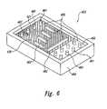
- FIG. 6is a partially schematic, top isometric view of a device package having an encapsulating material with heat transfer structures in accordance with yet another embodiment of the invention.
- the present disclosuredescribes packaged microelectronic devices and methods and apparatuses for packaging such devices. Many specific details of certain embodiments of the invention are set forth in the following description and in FIGS. 2-6 to provide a thorough understanding of these embodiments. One skilled in the art, however, will understand that the present invention may have additional embodiments, or that the invention may be practiced without several of the details described below.
- FIG. 2is a partially schematic, cross-sectional side elevational view of a device package 150 having a microelectronic substrate 120 (such as a memory die or a processor die) with an exposed upper surface 121 .
- the microelectronic substrate 120has a lower surface 122 facing opposite the upper surface 121 .
- the lower surface 122can include substrate bond pads 124 coupled to device features such as integrated circuits (not visible in FIG. 2 ) internal to the microelectronic substrate 120 .
- the microelectronic substrate 120can be mounted to a support member 130 (such as a PCB) by attaching an adhesive 123 between the lower surface 122 of the microelectronic substrate 120 and an upper surface of the support member 130 .
- the support member 130can have support member bond pads 133 connected to the substrate bond pads 124 with wire bonds 134 . Accordingly, the support member 130 can have an aperture 131 adjacent to the support member bond pads 133 through which the wire bonds 134 pass.
- the support member bond pads 133are connected to solder ball pads 132 with circuitry (not visible in FIG. 2 ) internal to the support member 130 to form a conductive link between the support member bond pads 133 and the solder ball pads 132 .
- Solder balls 135can then be attached to the solder ball pads 132 for coupling the device package 150 to other electronic components, as described above.
- the device package 150can have other conductive elements for coupling to other electronic components.
- portions of the microelectronic substrate 120 and the support member 130are surrounded by an encapsulating material 160 to protect features of the device package 150 .
- the encapsulating material 160can include an epoxy mold compound that covers the substrate bond pads 124 , the wire bonds 134 , and the support member bond pads 133 after the wire bonds 134 have been connected between the microelectronic substrate 120 and the support member 130 . Accordingly, the encapsulating material 160 can protect the electrical connection formed by the wire bonds 134 from corrosion and/or other environmental hazards.
- the encapsulating material 160is removed from the device package 150 in a region adjacent to the upper surface 121 of the microelectronic substrate 120 .
- the encapsulating material 160can have an opening 163 aligned with the upper surface 121 .
- the opening 163extends through the encapsulating material 160 to the upper surface 121 to expose the upper surface 121 .
- a thin layer of the encapsulating material 160can remain adjacent to the upper surface 121 of the microelectronic substrate 120 by removing a layer of encapsulating material 160 having a thickness less than the total thickness of the encapsulating material 160 adjacent to the upper surface 121 .
- the thickness of the removed layercan be greater than 0.003 inch in one embodiment, and can have other values in other embodiments, depending on the total thickness of the encapsulating material 160 .
- a sufficient amount of the encapsulating material 160can be removed from the region adjacent to the upper surface 121 to increase the rate at which heat can be transferred away from the upper surface 121 .
- the opening 163 in the encapsulating material 160is formed by positioning a laser source 170 proximate to the package 150 and directing a laser beam 171 toward the upper surface 121 of the microelectronic substrate 120 .
- the laser beam 171locally ablates the encapsulating material 160 , forming a vapor 172 that can be convected away from the region adjacent to the device package 150 .
- the opening 163can be formed by repeatedly passing the laser beam 171 over the device package 150 , with each successive pass removing a portion of the encapsulating material 160 until the opening 163 has the desired dimensions.
- the entire opening 163can be formed with a single pass of the laser beam 171 .
- a single opening 163can extend over all or a portion of the upper surface 121 of the microelectronic substrate 120 .
- the opening 163can be one of a plurality of openings, each of which extends over a portion of the upper surface 121 .
- the aperture 163can extend over the entire upper surface of the package 150 so that the encapsulating material does not extend upwardly beyond the upper surface 121 of the microelectronic substrate 120 .
- the power generated by the laser source 170can be from about 4 watts to about 25 watts, and the laser beam 171 can scan over the device package 150 at a rate of from about 125 mm/sec. to about 2000 mm/sec. Adjacent scans can be about 0.025 inches wide and the laser beam 171 can be pulsed at a frequency of from about 4 kHz to about 25 kHz with a pulse width of about 8 microseconds. In other embodiments, the laser source 170 can generate laser beams 171 having other characteristics suitable for removing the encapsulating material 160 .
- other techniquescan be used to remove a portion of the encapsulating material 160 to form the opening 163 .
- radiation having wavelengths other than laser wavelengthscan be directed toward the encapsulating material 160 .
- chemical solvents, such as etchantscan be used to selectively remove portions of the encapsulating material 160 from adjacent to the substrate upper surface 121 to form the opening 163 .
- the techniques used to remove portions of the encapsulating material 160are employed in a manner that does not adversely affect the operability of the microelectronic substrate 120 .
- One feature of an embodiment of the device package 150 described above with reference to FIG. 2is that the upper surface of the microelectronic substrate 120 is either exposed or has only a thin layer of encapsulating material 160 adjacent to it.
- An advantage of this featureis that heat can be more effectively and efficiently removed from the microelectronic substrate 120 , for example, by convection or radiation from the substrate upper surface 121 .
- a heat conductive heat sinkcan be attached to the exposed upper surface 121 to further increase the rate at which heat is transferred away from the microelectronic substrate 120 .
- the increased rate at which heat is transferred away from the microelectronic substrate 120can enhance the performance level and/or the life expectancy of the microelectronic substrate.
- FIG. 3Ais a partially schematic, cross-sectional side elevational view of a mold apparatus 140 for encapsulating the microelectronic substrate 120 in accordance with an embodiment of the invention.
- the mold apparatus 140can include an upper mold portion 141 configured to engage an upper surface 136 of the support member 130 .
- the upper mold portion 141can have an upper cavity 143 configured to receive the microelectronic substrate 120 .
- a lower mold portion 142is positioned opposite the upper mold portion 141 to engage a lower surface 137 of the support member 130 .
- the lower mold portion 142can include a lower cavity 144 configured to receive the wire bonds 134 , the support member bond pads 133 and the solder ball pads 132 .
- the encapsulating material 160when introduced into the mold apparatus 140 , it flows around the microelectronic substrate 120 and the connections between the microelectronic substrate 120 and the support member 130 to cover the wire bonds 134 , the support member bond pads 133 and at least a substantial portion of the solder ball pads 132 .
- the edges of the upper cavity 143are aligned with corresponding edges of the lower cavity 144 . Accordingly, the edges of the upper cavity 143 define upper contact portions 146 a that are aligned with lower contact portions 146 b defined by the edges of the lower cavity 144 .
- the support member 130is clamped uniformly from above and below. This is unlike some conventional arrangements (such as the arrangement described above with reference to FIG. 1A ) that have asymmetrically clamped PCBs that can allow portions of encapsulating material (flash) to penetrate between the PCB and the contact portions of the mold.
- the device package 150is removed from the mold apparatus 140 ( FIG. 3A ) after encapsulation and a portion of the encapsulating material 160 adjacent to the solder ball pads 132 is removed to expose the solder ball pads 132 for attaching solder balls 135 ( FIG. 2 ).
- the laser source 170can direct the laser beam 171 toward the encapsulating material 160 adjacent to the solder ball pads 132 to remove the encapsulating material 160 from this region.
- etchants or other chemical agents or other non-chemical agentscan remove selected portions of the encapsulating material 160 , so long as the surfaces of the exposed solder ball pads 132 are sufficiently clean to adhere to the solder balls 135 .
- an apparatus similar to that described above with reference to FIG. 1Acan be used to encapsulate the microelectronic substrate 120 , even if the resulting package has flash extending over the solder ball pads 132 .
- the laser source 170(or another agent for removing the encapsulating material 160 ) can remove the flash from the solder ball pads 132 .
- An advantage of using the mold apparatus described above with reference to FIG. 1Ais that existing mold apparatuses having this configuration can be used without alteration.
- an advantage of the apparatus 140 described above with reference to FIG. 3Ais that it can support the support member 130 equally from above and below, and can accordingly reduce the likelihood for inducing stresses in the microelectronic substrate 120 .
- FIG. 4is a partially schematic, cross-sectional side elevational view of two device packages positioned to form a stack 290 in accordance with an embodiment of the invention.
- the stack 290can include an upper package 250 a stacked on a lower package 250 b (referred to collectively as device packages 250 ).
- the device packages 250are held in place relative to each other with corresponding interlocking features 251 (shown as an upper portion feature 251 a and a lower portion feature 251 b ).
- each package 250can include a support member 230 (such as a PCB), a microelectronic substrate 220 attached to the support member 230 , and a volume of encapsulating material 260 having an upper portion 260 a above the support member 230 and a lower portion 260 b below the support member 230 .
- the upper portion 260 acan have an upper portion feature 251 a that interlocks with a corresponding lower portion feature 251 b in the lower portion 260 b to resist relative motion between the two device packages 250 .
- the upper portion feature 251 acan include a tab or projection
- the lower portion feature 251 bcan include a recess or cavity sized and shaped to removably receive the projection.
- the features 251can have other interlocking configurations.
- each device package 250can have more than one feature 251 to engage the adjacent device package.
- one characteristic of the interlocking features 251is that they can be molded directly into the encapsulating material 260 . Accordingly, the position of the features 251 can be consistent from one package 250 to the next, providing greater assurance that the packages will be properly aligned when stacked.
- the interlocking featurescan be formed by removing a portion of the encapsulating material 260 , for example, with a laser or a chemical process.
- another characteristic of the interlocking features 251is that they are integrated in the packages 250 . As a result, the packages 250 can be stacked without requiring additional jigs or tools, which can be time consuming to position and operate, and can cause damage to the packages 250 if handled improperly.
- FIG. 5is a partially schematic, cross-sectional side elevational view of two device packages 350 (shown as an upper package 350 a and a lower package 350 b ) positioned to form a stack 390 in accordance with another embodiment of the invention.
- each device package 350can include a support member 330 , a microelectronic substrate 320 on the support member 330 , and an encapsulating material 360 surrounding the microelectronic substrate 320 .
- the encapsulating material 360can be disposed on only an upper surface 336 of the support member 330 and not a lower surface 337 . Accordingly, the encapsulating material 360 can include an upper interlocking feature 351 a and the support member 330 can include a corresponding lower interlocking feature 351 b (referred to collectively as interlocking features 351 ).
- the lower interlocking feature 351 bcan include a cavity or recess in the lower surface 337 of the support member 330 .
- the cavitycan be sized and shaped to accommodate a portion of the encapsulating material 360 , without altering the encapsulating material 360 from a conventional shape.
- the upper interlocking feature 351 bcan be defined by a conventionally-shaped volume of encapsulating material 360 .
- the lower interlocking feature 351 bcan be sized and shaped to accommodate an upper interlocking feature 351 a that has a specialized shape, for example, a protrusion generally similar to that described above with reference to FIG. 4 .
- the interlocking features 351can have other shapes and configurations, so long as the interlocking features 351 at least resist relative motion between the packages 350 and provide for alignment of the packages 350 .
- FIG. 6is a partially schematic, top isometric view of a device package 450 having heat transfer structures 480 in accordance with another embodiment of the invention.
- the device package 450includes a microelectronic substrate 420 at least partially enclosed with an encapsulating material 460 .
- a portion of the encapsulating material 460 adjacent to an upper surface 421 of the microelectronic substrate 420is removed to form a cavity 463 that exposes at least a portion of the upper surface 421 .
- a thin layer 466 of encapsulating material 460can remain adjacent to the upper surface 421 .
- the encapsulating material 460can also be formed into the heat transfer structures 480 .
- the heat transfer structures 480can include pins 481 that project away from the upper surface 421 of the microelectronic substrate 420 , or project away from the thin layer 466 of encapsulating material 460 .
- the thin layer 466can also transfer heat away from the microelectronic substrate 420 , either alone or in conjunction with other heat transfer structures 480 .
- the heat transfer structures 480can include ribs 482 that project away from the microelectronic substrate 420 , or alternatively the heat transfer structures 480 can have other shapes and/or configurations for enhancing the rate at which heat is transferred away from the microelectronic substrate 420 .
- the heat transfer structures 480can be formed with a laser process or a chemical or non-chemical process similar to those described above with reference to FIGS. 2-3 .
- the heat transfer structures 480can be formed according to other techniques, for example, by molding the heat transfer structures directly into the encapsulating material 460 .
- the heat transfer structures 480can be formed directly on the upper surface 421 of the microelectronic substrate 420 .
- the heat transfer structures 480can be positioned on a thin layer 466 directly adjacent to the upper surface 421 .
- An advantage of either arrangementis that heat can be transferred more directly from the microelectronic substrate 420 to the heat transfer structures 480 and from the heat transfer structures 480 to the surrounding environment than in conventional arrangements that do not include the heat transfer structures 480 .
- the heat transfer structures 480can be formed directly in the encapsulating material 460 that surrounds the microelectronic substrate 420 .
- An advantage of this featureis that a separate heat transfer structure (such as a heat sink) need not be separately attached to the microelectronic substrate 420 . Accordingly, the thermal connection between the heat transfer structures 480 and the microelectronic substrate 420 can be more secure and thermally transmissive than a connection formed by attaching an initially separate heat sink.
- microelectronic substrates described above with reference to FIGS. 2-6can be supported by support members other than PCBs, including lead frames.
- the bond pads, solder ball pads, solder balls, and wire bondscan be replaced with electrically conductive terminals and connectors having other shapes and configurations.
- many of the features described above with reference to FIGS. 2-6can be combined in accordance with further embodiments of the invention.
- an embodiment of a microelectronic device packagecan include heat transfer structures in addition to interlocking features. Accordingly, the invention is not limited except as by the appended claims.
Landscapes
- Engineering & Computer Science (AREA)
- Microelectronics & Electronic Packaging (AREA)
- Power Engineering (AREA)
- Physics & Mathematics (AREA)
- Condensed Matter Physics & Semiconductors (AREA)
- General Physics & Mathematics (AREA)
- Computer Hardware Design (AREA)
- Manufacturing & Machinery (AREA)
- Encapsulation Of And Coatings For Semiconductor Or Solid State Devices (AREA)
Abstract
Description
Claims (25)
Priority Applications (3)
| Application Number | Priority Date | Filing Date | Title |
|---|---|---|---|
| US09/639,917US7273769B1 (en) | 2000-08-16 | 2000-08-16 | Method and apparatus for removing encapsulating material from a packaged microelectronic device |
| US10/217,667US7405487B2 (en) | 2000-08-16 | 2002-08-12 | Method and apparatus for removing encapsulating material from a packaged microelectronic device |
| US11/580,451US20070031998A1 (en) | 2000-08-16 | 2006-10-12 | Method and apparatus for removing encapsulating material from a packaged microelectronic device |
Applications Claiming Priority (1)
| Application Number | Priority Date | Filing Date | Title |
|---|---|---|---|
| US09/639,917US7273769B1 (en) | 2000-08-16 | 2000-08-16 | Method and apparatus for removing encapsulating material from a packaged microelectronic device |
Related Child Applications (2)
| Application Number | Title | Priority Date | Filing Date |
|---|---|---|---|
| US10/217,667DivisionUS7405487B2 (en) | 2000-08-16 | 2002-08-12 | Method and apparatus for removing encapsulating material from a packaged microelectronic device |
| US11/580,451DivisionUS20070031998A1 (en) | 2000-08-16 | 2006-10-12 | Method and apparatus for removing encapsulating material from a packaged microelectronic device |
Publications (1)
| Publication Number | Publication Date |
|---|---|
| US7273769B1true US7273769B1 (en) | 2007-09-25 |
Family
ID=24566102
Family Applications (3)
| Application Number | Title | Priority Date | Filing Date |
|---|---|---|---|
| US09/639,917Expired - LifetimeUS7273769B1 (en) | 2000-08-16 | 2000-08-16 | Method and apparatus for removing encapsulating material from a packaged microelectronic device |
| US10/217,667Expired - LifetimeUS7405487B2 (en) | 2000-08-16 | 2002-08-12 | Method and apparatus for removing encapsulating material from a packaged microelectronic device |
| US11/580,451AbandonedUS20070031998A1 (en) | 2000-08-16 | 2006-10-12 | Method and apparatus for removing encapsulating material from a packaged microelectronic device |
Family Applications After (2)
| Application Number | Title | Priority Date | Filing Date |
|---|---|---|---|
| US10/217,667Expired - LifetimeUS7405487B2 (en) | 2000-08-16 | 2002-08-12 | Method and apparatus for removing encapsulating material from a packaged microelectronic device |
| US11/580,451AbandonedUS20070031998A1 (en) | 2000-08-16 | 2006-10-12 | Method and apparatus for removing encapsulating material from a packaged microelectronic device |
Country Status (1)
| Country | Link |
|---|---|
| US (3) | US7273769B1 (en) |
Cited By (6)
| Publication number | Priority date | Publication date | Assignee | Title |
|---|---|---|---|---|
| US20050199992A1 (en)* | 2004-03-12 | 2005-09-15 | Baek Joong-Hyun | Semiconductor stack package and memory module with improved heat dissipation |
| US20050233497A1 (en)* | 2002-08-22 | 2005-10-20 | Intel Corporation | Method of forming a multi-die semiconductor package |
| US20060022333A1 (en)* | 2000-03-17 | 2006-02-02 | International Rectifier Corporation | Semiconductor multichip module package with improved thermal performance; reduced size and improved moisture resistance |
| US20080017961A1 (en)* | 2006-07-20 | 2008-01-24 | Chipmos Technologies Inc. | Chip package structure and manufacturing method thereof |
| US20110277980A1 (en)* | 2008-09-30 | 2011-11-17 | Intel Corporation | Microfins for cooling an ultramobile device |
| CN110690127A (en)* | 2014-03-14 | 2020-01-14 | 台湾积体电路制造股份有限公司 | Packaged semiconductor device and packaging method thereof |
Families Citing this family (35)
| Publication number | Priority date | Publication date | Assignee | Title |
|---|---|---|---|---|
| JP4251421B2 (en)* | 2000-01-13 | 2009-04-08 | 新光電気工業株式会社 | Manufacturing method of semiconductor device |
| JP3405456B2 (en)* | 2000-09-11 | 2003-05-12 | 沖電気工業株式会社 | Semiconductor device, method of manufacturing semiconductor device, stack type semiconductor device, and method of manufacturing stack type semiconductor device |
| KR100480909B1 (en)* | 2001-12-29 | 2005-04-07 | 주식회사 하이닉스반도체 | method for manufacturing stacked chip package |
| US6950305B2 (en)* | 2002-05-15 | 2005-09-27 | Bel Fuse, Inc. | Overmolded device with contoured surface |
| EP1664817A1 (en)* | 2003-09-16 | 2006-06-07 | Koninklijke Philips Electronics N.V. | A method of manufacturing an electronic device and an electronic device |
| DE102004044882B3 (en)* | 2004-09-14 | 2006-04-20 | Infineon Technologies Ag | Semiconductor module having stacked semiconductor devices and electrical interconnects between the stacked semiconductor devices |
| EP1659627A1 (en)* | 2004-11-23 | 2006-05-24 | Optimum Care International Tech. Inc. | chip scale package |
| KR100626618B1 (en) | 2004-12-10 | 2006-09-25 | 삼성전자주식회사 | Semiconductor chip stack package and manufacturing method |
| FR2893764B1 (en)* | 2005-11-21 | 2008-06-13 | St Microelectronics Sa | STACKABLE SEMICONDUCTOR HOUSING AND METHOD FOR MANUFACTURING THE SAME |
| US7880317B2 (en)* | 2005-11-22 | 2011-02-01 | Sony Corporation | Semiconductor device and method of manufacturing semiconductor device |
| US20070216008A1 (en)* | 2006-03-20 | 2007-09-20 | Gerber Mark A | Low profile semiconductor package-on-package |
| US20070241441A1 (en)* | 2006-04-17 | 2007-10-18 | Stats Chippac Ltd. | Multichip package system |
| US7714453B2 (en)* | 2006-05-12 | 2010-05-11 | Broadcom Corporation | Interconnect structure and formation for package stacking of molded plastic area array package |
| US8581381B2 (en)* | 2006-06-20 | 2013-11-12 | Broadcom Corporation | Integrated circuit (IC) package stacking and IC packages formed by same |
| US7638868B2 (en) | 2006-08-16 | 2009-12-29 | Tessera, Inc. | Microelectronic package |
| US8299626B2 (en) | 2007-08-16 | 2012-10-30 | Tessera, Inc. | Microelectronic package |
| KR20090025908A (en)* | 2007-09-07 | 2009-03-11 | 삼성전자주식회사 | Electronic device having stacked semiconductor package and method for forming same |
| US9136259B2 (en)* | 2008-04-11 | 2015-09-15 | Micron Technology, Inc. | Method of creating alignment/centering guides for small diameter, high density through-wafer via die stacking |
| EP2337851B1 (en) | 2008-09-29 | 2014-08-13 | Butamax Advanced Biofuels Llc | IDENTIFICATION AND USE OF BACTERIAL Ý2Fe-2S¨DIHYDROXY-ACID DEHYDRATASES |
| US8263434B2 (en) | 2009-07-31 | 2012-09-11 | Stats Chippac, Ltd. | Semiconductor device and method of mounting die with TSV in cavity of substrate for electrical interconnect of Fi-PoP |
| US20110089152A1 (en)* | 2009-10-16 | 2011-04-21 | Control Systemation, Inc. | Method and system for exposing delicate structures of a device encapsulated in a mold compound |
| US20120018901A1 (en)* | 2010-07-21 | 2012-01-26 | Lsi Corporation | Flip-chip package and method of manufacturing the same using ablation |
| WO2012162369A1 (en)* | 2011-05-23 | 2012-11-29 | University Of Massachusetts | Apparatus and methods for multi-scale alignment and fastening |
| US8872318B2 (en) | 2011-08-24 | 2014-10-28 | Tessera, Inc. | Through interposer wire bond using low CTE interposer with coarse slot apertures |
| FR2987170A1 (en)* | 2012-02-17 | 2013-08-23 | St Microelectronics Grenoble 2 | ELECTRONIC HOUSING AND DEVICE |
| US8842951B2 (en) | 2012-03-02 | 2014-09-23 | Analog Devices, Inc. | Systems and methods for passive alignment of opto-electronic components |
| US9716193B2 (en) | 2012-05-02 | 2017-07-25 | Analog Devices, Inc. | Integrated optical sensor module |
| US10884551B2 (en) | 2013-05-16 | 2021-01-05 | Analog Devices, Inc. | Integrated gesture sensor module |
| US9590129B2 (en) | 2014-11-19 | 2017-03-07 | Analog Devices Global | Optical sensor module |
| US9899236B2 (en) | 2014-12-24 | 2018-02-20 | Stmicroelectronics, Inc. | Semiconductor package with cantilever pads |
| US9768126B2 (en)* | 2014-12-24 | 2017-09-19 | Stmicroelectronics, Inc. | Stacked semiconductor packages with cantilever pads |
| CN110335823A (en)* | 2015-05-26 | 2019-10-15 | 意法半导体公司 | Stacked semiconductor package with cantilever pad |
| US10694633B2 (en)* | 2017-11-15 | 2020-06-23 | Regal Beloit America, Inc. | Motor controller and method for assembling the same |
| US10712197B2 (en) | 2018-01-11 | 2020-07-14 | Analog Devices Global Unlimited Company | Optical sensor package |
| KR102600154B1 (en)* | 2019-06-12 | 2023-11-07 | 삼성전자주식회사 | Semiconductor package |
Citations (127)
| Publication number | Priority date | Publication date | Assignee | Title |
|---|---|---|---|---|
| JPS57211259A (en)* | 1981-06-23 | 1982-12-25 | Toshiba Corp | Semiconductor device |
| JPS58100447A (en)* | 1981-12-11 | 1983-06-15 | Hitachi Ltd | Resin-encapsulated semiconductor device and its manufacturing method |
| US4560580A (en) | 1982-09-30 | 1985-12-24 | Phillips Petroleum Company | Process for encapsulating articles with optional laser printing |
| JPS61114563A (en)* | 1984-11-09 | 1986-06-02 | Nec Corp | Integrated circuit package |
| US5041902A (en)* | 1989-12-14 | 1991-08-20 | Motorola, Inc. | Molded electronic package with compression structures |
| JPH03208363A (en)* | 1990-01-10 | 1991-09-11 | Hitachi Ltd | Mark correction method and marking method |
| US5138434A (en) | 1991-01-22 | 1992-08-11 | Micron Technology, Inc. | Packaging for semiconductor logic devices |
| FR2673040A1 (en) | 1991-02-19 | 1992-08-21 | Thomson Csf | Method of assembling and interconnecting modular electronic cards, cards and set of electronic cards according to this method |
| JPH0547963A (en) | 1991-08-20 | 1993-02-26 | Rohm Co Ltd | Package |
| US5254500A (en)* | 1991-02-05 | 1993-10-19 | Advanced Micro Devices, Inc. | Method for making an integrally molded semiconductor device heat sink |
| US5296740A (en)* | 1991-03-20 | 1994-03-22 | Fujitsu Limited | Method and apparatus for a semiconductor device having a radiation part |
| JPH06177268A (en)* | 1992-12-07 | 1994-06-24 | Fujitsu Ltd | Fabrication of semiconductor device |
| US5344795A (en) | 1992-09-22 | 1994-09-06 | Microelectronics And Computer Technology Corporation | Method for encapsulating an integrated circuit using a removable heatsink support block |
| US5371404A (en)* | 1993-02-04 | 1994-12-06 | Motorola, Inc. | Thermally conductive integrated circuit package with radio frequency shielding |
| US5394010A (en) | 1991-03-13 | 1995-02-28 | Kabushiki Kaisha Toshiba | Semiconductor assembly having laminated semiconductor devices |
| US5406117A (en)* | 1993-12-09 | 1995-04-11 | Dlugokecki; Joseph J. | Radiation shielding for integrated circuit devices using reconstructed plastic packages |
| US5438216A (en) | 1992-08-31 | 1995-08-01 | Motorola, Inc. | Light erasable multichip module |
| US5483098A (en)* | 1992-04-21 | 1996-01-09 | Motorola, Inc. | Drop-in heat sink package with window frame flag |
| US5536685A (en) | 1994-09-20 | 1996-07-16 | Sun Microsystems, Inc. | Low heat loss and secure chip carrier for cryogenic cooling |
| JPH08213520A (en) | 1995-02-03 | 1996-08-20 | Mitsubishi Electric Corp | Semiconductor device and manufacturing method thereof |
| US5593927A (en) | 1993-10-14 | 1997-01-14 | Micron Technology, Inc. | Method for packaging semiconductor dice |
| US5604376A (en)* | 1994-06-30 | 1997-02-18 | Digital Equipment Corporation | Paddleless molded plastic semiconductor chip package |
| US5622873A (en) | 1994-01-24 | 1997-04-22 | Goldstar Electron Co., Ltd. | Process for manufacturing a resin molded image pick-up semiconductor chip having a window |
| US5677566A (en) | 1995-05-08 | 1997-10-14 | Micron Technology, Inc. | Semiconductor chip package |
| US5696033A (en) | 1995-08-16 | 1997-12-09 | Micron Technology, Inc. | Method for packaging a semiconductor die |
| US5723900A (en)* | 1993-09-06 | 1998-03-03 | Sony Corporation | Resin mold type semiconductor device |
| US5739585A (en) | 1995-11-27 | 1998-04-14 | Micron Technology, Inc. | Single piece package for semiconductor die |
| US5754408A (en) | 1995-11-29 | 1998-05-19 | Mitsubishi Semiconductor America, Inc. | Stackable double-density integrated circuit assemblies |
| USD394844S (en) | 1997-04-25 | 1998-06-02 | Micron Technology, Inc. | Temporary package for semiconductor dice |
| US5777391A (en) | 1994-12-20 | 1998-07-07 | Hitachi, Ltd. | Semiconductor device having an improved connection arrangement between a semiconductor pellet and base substrate electrodes and a method of manufacture thereof |
| US5790381A (en) | 1995-12-15 | 1998-08-04 | Mitsubishi Semiconductor America, Inc. | Integrated circuit package assembly |
| USD402638S (en) | 1997-04-25 | 1998-12-15 | Micron Technology, Inc. | Temporary package for semiconductor dice |
| US5851845A (en) | 1995-12-18 | 1998-12-22 | Micron Technology, Inc. | Process for packaging a semiconductor die using dicing and testing |
| US5866953A (en) | 1996-05-24 | 1999-02-02 | Micron Technology, Inc. | Packaged die on PCB with heat sink encapsulant |
| US5891753A (en) | 1997-01-24 | 1999-04-06 | Micron Technology, Inc. | Method and apparatus for packaging flip chip bare die on printed circuit boards |
| US5893726A (en) | 1997-12-15 | 1999-04-13 | Micron Technology, Inc. | Semiconductor package with pre-fabricated cover and method of fabrication |
| US5925934A (en)* | 1995-10-28 | 1999-07-20 | Institute Of Microelectronics | Low cost and highly reliable chip-sized package |
| US5933713A (en) | 1998-04-06 | 1999-08-03 | Micron Technology, Inc. | Method of forming overmolded chip scale package and resulting product |
| US5938956A (en) | 1996-09-10 | 1999-08-17 | Micron Technology, Inc. | Circuit and method for heating an adhesive to package or rework a semiconductor die |
| US5952714A (en) | 1995-08-02 | 1999-09-14 | Matsushita Electronics Corporation | Solid-state image sensing apparatus and manufacturing method thereof |
| US5958100A (en) | 1993-06-03 | 1999-09-28 | Micron Technology, Inc. | Process of making a glass semiconductor package |
| US5962810A (en) | 1997-09-09 | 1999-10-05 | Amkor Technology, Inc. | Integrated circuit package employing a transparent encapsulant |
| US5986209A (en) | 1997-07-09 | 1999-11-16 | Micron Technology, Inc. | Package stack via bottom leaded plastic (BLP) packaging |
| US5990566A (en) | 1998-05-20 | 1999-11-23 | Micron Technology, Inc. | High density semiconductor package |
| US5989941A (en) | 1997-12-12 | 1999-11-23 | Micron Technology, Inc. | Encapsulated integrated circuit packaging |
| US5994784A (en) | 1997-12-18 | 1999-11-30 | Micron Technology, Inc. | Die positioning in integrated circuit packaging |
| US6008070A (en) | 1998-05-21 | 1999-12-28 | Micron Technology, Inc. | Wafer level fabrication and assembly of chip scale packages |
| USRE36469E (en) | 1988-09-30 | 1999-12-28 | Micron Technology, Inc. | Packaging for semiconductor logic devices |
| US6020629A (en) | 1998-06-05 | 2000-02-01 | Micron Technology, Inc. | Stacked semiconductor package and method of fabrication |
| US6025728A (en) | 1997-04-25 | 2000-02-15 | Micron Technology, Inc. | Semiconductor package with wire bond protective member |
| US6028365A (en) | 1998-03-30 | 2000-02-22 | Micron Technology, Inc. | Integrated circuit package and method of fabrication |
| US6046496A (en) | 1997-11-04 | 2000-04-04 | Micron Technology Inc | Chip package |
| US6049125A (en) | 1997-12-29 | 2000-04-11 | Micron Technology, Inc. | Semiconductor package with heat sink and method of fabrication |
| US6049129A (en)* | 1997-12-19 | 2000-04-11 | Texas Instruments Incorporated | Chip size integrated circuit package |
| US6048744A (en) | 1997-09-15 | 2000-04-11 | Micron Technology, Inc. | Integrated circuit package alignment feature |
| US6048755A (en) | 1998-11-12 | 2000-04-11 | Micron Technology, Inc. | Method for fabricating BGA package using substrate with patterned solder mask open in die attach area |
| US6072236A (en) | 1996-03-07 | 2000-06-06 | Micron Technology, Inc. | Micromachined chip scale package |
| US6075288A (en) | 1998-06-08 | 2000-06-13 | Micron Technology, Inc. | Semiconductor package having interlocking heat sinks and method of fabrication |
| US6093029A (en) | 1998-09-08 | 2000-07-25 | S3 Incorporated | Vertically stackable integrated circuit |
| US6093969A (en)* | 1999-05-15 | 2000-07-25 | Lin; Paul T. | Face-to-face (FTF) stacked assembly of substrate-on-bare-chip (SOBC) modules |
| US6097087A (en) | 1997-10-31 | 2000-08-01 | Micron Technology, Inc. | Semiconductor package including flex circuit, interconnects and dense array external contacts |
| US6103547A (en) | 1997-01-17 | 2000-08-15 | Micron Technology, Inc. | High speed IC package configuration |
| US6107122A (en) | 1997-08-04 | 2000-08-22 | Micron Technology, Inc. | Direct die contact (DDC) semiconductor package |
| US6107680A (en) | 1995-01-04 | 2000-08-22 | Micron Technology, Inc. | Packaging for bare dice employing EMR-sensitive adhesives |
| US6117797A (en)* | 1998-09-03 | 2000-09-12 | Micron Technology, Inc. | Attachment method for heat sinks and devices involving removal of misplaced encapsulant |
| US6117382A (en) | 1998-02-05 | 2000-09-12 | Micron Technology, Inc. | Method for encasing array packages |
| US6122171A (en) | 1999-07-30 | 2000-09-19 | Micron Technology, Inc. | Heat sink chip package and method of making |
| US6148509A (en) | 1997-04-07 | 2000-11-21 | Micron Technology, Inc. | Method for supporting an integrated circuit die |
| US6153924A (en) | 1998-02-23 | 2000-11-28 | Micron Technology, Inc. | Multilayered lead frame for semiconductor package |
| US6159764A (en) | 1997-07-02 | 2000-12-12 | Micron Technology, Inc. | Varied-thickness heat sink for integrated circuit (IC) packages and method of fabricating IC packages |
| US6159770A (en) | 1995-11-08 | 2000-12-12 | Fujitsu Limited | Method and apparatus for fabricating semiconductor device |
| US6163956A (en) | 1998-02-23 | 2000-12-26 | Micron Technology, Inc. | Method of making chip scale package with heat spreade |
| US6172419B1 (en) | 1998-02-24 | 2001-01-09 | Micron Technology, Inc. | Low profile ball grid array package |
| US6175159B1 (en) | 1997-07-16 | 2001-01-16 | Oki Electric Industry Co., Ltd. | Semiconductor package |
| US6177726B1 (en) | 1999-02-11 | 2001-01-23 | Philips Electronics North America Corporation | SiO2 wire bond insulation in semiconductor assemblies |
| US6184465B1 (en) | 1998-11-12 | 2001-02-06 | Micron Technology, Inc. | Semiconductor package |
| US6198172B1 (en) | 1997-02-20 | 2001-03-06 | Micron Technology, Inc. | Semiconductor chip package |
| US6198171B1 (en)* | 1999-12-30 | 2001-03-06 | Siliconware Precision Industries Co., Ltd. | Thermally enhanced quad flat non-lead package of semiconductor |
| US6208519B1 (en) | 1999-08-31 | 2001-03-27 | Micron Technology, Inc. | Thermally enhanced semiconductor package |
| US6210992B1 (en) | 1999-08-31 | 2001-04-03 | Micron Technology, Inc. | Controlling packaging encapsulant leakage |
| US6215175B1 (en) | 1998-07-06 | 2001-04-10 | Micron Technology, Inc. | Semiconductor package having metal foil die mounting plate |
| US6218731B1 (en)* | 1999-05-21 | 2001-04-17 | Siliconware Precision Industries Co., Ltd. | Tiny ball grid array package |
| US6228548B1 (en) | 1998-02-27 | 2001-05-08 | Micron Technology, Inc. | Method of making a multichip semiconductor package |
| US6229202B1 (en) | 2000-01-10 | 2001-05-08 | Micron Technology, Inc. | Semiconductor package having downset leadframe for reducing package bow |
| US6228676B1 (en)* | 1996-10-31 | 2001-05-08 | Amkor Technology, Inc. | Near chip size integrated circuit package |
| US6249433B1 (en)* | 1999-05-14 | 2001-06-19 | Siliconware Precision Industries | Heat-dissipating device for integrated circuit package |
| US6252772B1 (en) | 1999-02-10 | 2001-06-26 | Micron Technology, Inc. | Removable heat sink bumpers on a quad flat package |
| US6259153B1 (en) | 1998-08-20 | 2001-07-10 | Micron Technology, Inc. | Transverse hybrid LOC package |
| US20010013639A1 (en) | 1998-12-21 | 2001-08-16 | Masaaki Abe | Ball-grid-array semiconductor with protruding terminals |
| US6277671B1 (en) | 1998-10-20 | 2001-08-21 | Micron Technology, Inc. | Methods of forming integrated circuit packages |
| US6284571B1 (en) | 1997-07-02 | 2001-09-04 | Micron Technology, Inc. | Lead frame assemblies with voltage reference plane and IC packages including same |
| US6291894B1 (en) | 1998-08-31 | 2001-09-18 | Micron Technology, Inc. | Method and apparatus for a semiconductor package for vertical surface mounting |
| US6294839B1 (en) | 1999-08-30 | 2001-09-25 | Micron Technology, Inc. | Apparatus and methods of packaging and testing die |
| US6303985B1 (en) | 1998-11-12 | 2001-10-16 | Micron Technology, Inc. | Semiconductor lead frame and package with stiffened mounting paddle |
| US6303981B1 (en) | 1999-09-01 | 2001-10-16 | Micron Technology, Inc. | Semiconductor package having stacked dice and leadframes and method of fabrication |
| US6309943B1 (en)* | 2000-04-25 | 2001-10-30 | Amkor Technology, Inc. | Precision marking and singulation method |
| US6310390B1 (en) | 1999-04-08 | 2001-10-30 | Micron Technology, Inc. | BGA package and method of fabrication |
| US6316285B1 (en) | 1998-09-02 | 2001-11-13 | Micron Technology, Inc. | Passivation layer for packaged integrated circuits |
| US6326244B1 (en) | 1998-09-03 | 2001-12-04 | Micron Technology, Inc. | Method of making a cavity ball grid array apparatus |
| US6326700B1 (en)* | 2000-08-15 | 2001-12-04 | United Test Center, Inc. | Low profile semiconductor package and process for making the same |
| US6326687B1 (en) | 1998-09-01 | 2001-12-04 | Micron Technology, Inc. | IC package with dual heat spreaders |
| US6326698B1 (en) | 2000-06-08 | 2001-12-04 | Micron Technology, Inc. | Semiconductor devices having protective layers thereon through which contact pads are exposed and stereolithographic methods of fabricating such semiconductor devices |
| US6329220B1 (en) | 1999-11-23 | 2001-12-11 | Micron Technology, Inc. | Packages for semiconductor die |
| US6331221B1 (en) | 1998-04-15 | 2001-12-18 | Micron Technology, Inc. | Process for providing electrical connection between a semiconductor die and a semiconductor die receiving member |
| US6331453B1 (en) | 1999-12-16 | 2001-12-18 | Micron Technology, Inc. | Method for fabricating semiconductor packages using mold tooling fixture with flash control cavities |
| US6335208B1 (en)* | 1999-05-10 | 2002-01-01 | Intersil Americas Inc. | Laser decapsulation method |
| US6335571B1 (en)* | 1997-07-21 | 2002-01-01 | Miguel Albert Capote | Semiconductor flip-chip package and method for the fabrication thereof |
| US6344976B1 (en) | 1997-04-07 | 2002-02-05 | Micron Technology, Inc. | Interdigitated leads-over-chip lead frame device and method for supporting an integrated circuit die |
| US6369455B1 (en)* | 2000-01-04 | 2002-04-09 | Siliconware Precision Industries Co., Ltd. | Externally-embedded heat-dissipating device for ball grid array integrated circuit package |
| US6379988B1 (en)* | 2000-05-16 | 2002-04-30 | Sandia Corporation | Pre-release plastic packaging of MEMS and IMEMS devices |
| US20020060369A1 (en) | 1999-09-02 | 2002-05-23 | Salman Akram | Board-on-chip packages with conductive foil on the chip surface |
| US6395584B2 (en)* | 1998-12-22 | 2002-05-28 | Ficta Technology Inc. | Method for improving the liquid dispensing of IC packages |
| US6414385B1 (en)* | 1999-11-08 | 2002-07-02 | Siliconware Precisionindustries Co., Ltd. | Quad flat non-lead package of semiconductor |
| US6420790B1 (en) | 1999-12-02 | 2002-07-16 | Oki Electric Industry Co., Ltd. | Semiconductor device |
| US6424031B1 (en)* | 2000-05-08 | 2002-07-23 | Amkor Technology, Inc. | Stackable package with heat sink |
| US6433419B2 (en)* | 1990-09-24 | 2002-08-13 | Tessera, Inc. | Face-up semiconductor chip assemblies |
| US20020173070A1 (en)* | 2000-08-21 | 2002-11-21 | Bolken Todd O. | Method and apparatus for encapsulating a multi-chip substrate array |
| US6486562B1 (en)* | 1999-06-07 | 2002-11-26 | Nec Corporation | Circuit device with bonding strength improved and method of manufacturing the same |
| US20020180035A1 (en)* | 2001-06-04 | 2002-12-05 | Siliconware Precision Industries Co., Ltd. | Semiconductor package with heat sink |
| US6518659B1 (en) | 2000-05-08 | 2003-02-11 | Amkor Technology, Inc. | Stackable package having a cavity and a lid for an electronic device |
| US6534861B1 (en)* | 1999-11-15 | 2003-03-18 | Substrate Technologies Incorporated | Ball grid substrate for lead-on-chip semiconductor package |
| US6544814B1 (en)* | 1999-07-27 | 2003-04-08 | Mitsubishi Denki Kabushiki Kaisha | Method of manufacturing a packaged semiconductor device, and a semiconductor device manufactured thereby |
| US20030080440A1 (en)* | 2000-05-31 | 2003-05-01 | Amkor Technology, Inc. | Reverse contrast marked package |
| US6667544B1 (en) | 2000-06-30 | 2003-12-23 | Amkor Technology, Inc. | Stackable package having clips for fastening package and tool for opening clips |
| US6774473B1 (en) | 1999-07-30 | 2004-08-10 | Ming-Tung Shen | Semiconductor chip module |
| US6778404B1 (en) | 2000-06-02 | 2004-08-17 | Micron Technology Inc | Stackable ball grid array |
| US20050148160A1 (en)* | 2002-03-06 | 2005-07-07 | Farnworth Warren M. | Encapsulated semiconductor components and methods of fabrication |
Family Cites Families (19)
| Publication number | Priority date | Publication date | Assignee | Title |
|---|---|---|---|---|
| JPS57147260A (en)* | 1981-03-05 | 1982-09-11 | Matsushita Electronics Corp | Manufacture of resin-sealed semiconductor device and lead frame used therefor |
| JPS6379354A (en)* | 1986-09-24 | 1988-04-09 | Hitachi Vlsi Eng Corp | Resin-sealed semiconductor device |
| JP2759523B2 (en)* | 1989-10-18 | 1998-05-28 | 株式会社三井ハイテック | Method for manufacturing semiconductor device |
| US5147821A (en)* | 1990-09-28 | 1992-09-15 | Motorola, Inc. | Method for making a thermally enhanced semiconductor device by holding a leadframe against a heatsink through vacuum suction in a molding operation |
| JP2876773B2 (en)* | 1990-10-22 | 1999-03-31 | セイコーエプソン株式会社 | Program instruction word length variable type computing device and data processing device |
| US5172303A (en)* | 1990-11-23 | 1992-12-15 | Motorola, Inc. | Electronic component assembly |
| US5768109A (en)* | 1991-06-26 | 1998-06-16 | Hughes Electronics | Multi-layer circuit board and semiconductor flip chip connection |
| US5410451A (en)* | 1993-12-20 | 1995-04-25 | Lsi Logic Corporation | Location and standoff pins for chip on tape |
| US5959845A (en)* | 1997-09-18 | 1999-09-28 | International Business Machines Corporation | Universal chip carrier connector |
| US5888850A (en)* | 1997-09-29 | 1999-03-30 | International Business Machines Corporation | Method for providing a protective coating and electronic package utilizing same |
| US6114221A (en)* | 1998-03-16 | 2000-09-05 | International Business Machines Corporation | Method and apparatus for interconnecting multiple circuit chips |
| US6049467A (en)* | 1998-08-31 | 2000-04-11 | Unisys Corporation | Stackable high density RAM modules |
| US6426642B1 (en)* | 1999-02-16 | 2002-07-30 | Micron Technology, Inc. | Insert for seating a microelectronic device having a protrusion and a plurality of raised-contacts |
| US6366467B1 (en)* | 2000-03-31 | 2002-04-02 | Intel Corporation | Dual-socket interposer and method of fabrication therefor |
| JP2001308260A (en)* | 2000-04-25 | 2001-11-02 | Seiko Epson Corp | Semiconductor device |
| US6979595B1 (en)* | 2000-08-24 | 2005-12-27 | Micron Technology, Inc. | Packaged microelectronic devices with pressure release elements and methods for manufacturing and using such packaged microelectronic devices |
| US6756005B2 (en)* | 2001-08-24 | 2004-06-29 | Cool Shield, Inc. | Method for making a thermally conductive article having an integrated surface and articles produced therefrom |
| US6950305B2 (en)* | 2002-05-15 | 2005-09-27 | Bel Fuse, Inc. | Overmolded device with contoured surface |
| TWI286832B (en)* | 2002-11-05 | 2007-09-11 | Advanced Semiconductor Eng | Thermal enhance semiconductor package |
- 2000
- 2000-08-16USUS09/639,917patent/US7273769B1/ennot_activeExpired - Lifetime
- 2002
- 2002-08-12USUS10/217,667patent/US7405487B2/ennot_activeExpired - Lifetime
- 2006
- 2006-10-12USUS11/580,451patent/US20070031998A1/ennot_activeAbandoned
Patent Citations (139)
| Publication number | Priority date | Publication date | Assignee | Title |
|---|---|---|---|---|
| JPS57211259A (en)* | 1981-06-23 | 1982-12-25 | Toshiba Corp | Semiconductor device |
| JPS58100447A (en)* | 1981-12-11 | 1983-06-15 | Hitachi Ltd | Resin-encapsulated semiconductor device and its manufacturing method |
| US4560580A (en) | 1982-09-30 | 1985-12-24 | Phillips Petroleum Company | Process for encapsulating articles with optional laser printing |
| JPS61114563A (en)* | 1984-11-09 | 1986-06-02 | Nec Corp | Integrated circuit package |
| USRE36469E (en) | 1988-09-30 | 1999-12-28 | Micron Technology, Inc. | Packaging for semiconductor logic devices |
| US5041902A (en)* | 1989-12-14 | 1991-08-20 | Motorola, Inc. | Molded electronic package with compression structures |
| JPH03208363A (en)* | 1990-01-10 | 1991-09-11 | Hitachi Ltd | Mark correction method and marking method |
| US6433419B2 (en)* | 1990-09-24 | 2002-08-13 | Tessera, Inc. | Face-up semiconductor chip assemblies |
| US5138434A (en) | 1991-01-22 | 1992-08-11 | Micron Technology, Inc. | Packaging for semiconductor logic devices |
| US5254500A (en)* | 1991-02-05 | 1993-10-19 | Advanced Micro Devices, Inc. | Method for making an integrally molded semiconductor device heat sink |
| FR2673040A1 (en) | 1991-02-19 | 1992-08-21 | Thomson Csf | Method of assembling and interconnecting modular electronic cards, cards and set of electronic cards according to this method |
| US5394010A (en) | 1991-03-13 | 1995-02-28 | Kabushiki Kaisha Toshiba | Semiconductor assembly having laminated semiconductor devices |
| US5296740A (en)* | 1991-03-20 | 1994-03-22 | Fujitsu Limited | Method and apparatus for a semiconductor device having a radiation part |
| JPH0547963A (en) | 1991-08-20 | 1993-02-26 | Rohm Co Ltd | Package |
| US5483098A (en)* | 1992-04-21 | 1996-01-09 | Motorola, Inc. | Drop-in heat sink package with window frame flag |
| US5438216A (en) | 1992-08-31 | 1995-08-01 | Motorola, Inc. | Light erasable multichip module |
| US5344795A (en) | 1992-09-22 | 1994-09-06 | Microelectronics And Computer Technology Corporation | Method for encapsulating an integrated circuit using a removable heatsink support block |
| JPH06177268A (en)* | 1992-12-07 | 1994-06-24 | Fujitsu Ltd | Fabrication of semiconductor device |
| US5371404A (en)* | 1993-02-04 | 1994-12-06 | Motorola, Inc. | Thermally conductive integrated circuit package with radio frequency shielding |
| US5958100A (en) | 1993-06-03 | 1999-09-28 | Micron Technology, Inc. | Process of making a glass semiconductor package |
| US5723900A (en)* | 1993-09-06 | 1998-03-03 | Sony Corporation | Resin mold type semiconductor device |
| US5593927A (en) | 1993-10-14 | 1997-01-14 | Micron Technology, Inc. | Method for packaging semiconductor dice |
| US5406117A (en)* | 1993-12-09 | 1995-04-11 | Dlugokecki; Joseph J. | Radiation shielding for integrated circuit devices using reconstructed plastic packages |
| US5622873A (en) | 1994-01-24 | 1997-04-22 | Goldstar Electron Co., Ltd. | Process for manufacturing a resin molded image pick-up semiconductor chip having a window |
| US5604376A (en)* | 1994-06-30 | 1997-02-18 | Digital Equipment Corporation | Paddleless molded plastic semiconductor chip package |
| US5536685A (en) | 1994-09-20 | 1996-07-16 | Sun Microsystems, Inc. | Low heat loss and secure chip carrier for cryogenic cooling |
| US5777391A (en) | 1994-12-20 | 1998-07-07 | Hitachi, Ltd. | Semiconductor device having an improved connection arrangement between a semiconductor pellet and base substrate electrodes and a method of manufacture thereof |
| US6107680A (en) | 1995-01-04 | 2000-08-22 | Micron Technology, Inc. | Packaging for bare dice employing EMR-sensitive adhesives |
| JPH08213520A (en) | 1995-02-03 | 1996-08-20 | Mitsubishi Electric Corp | Semiconductor device and manufacturing method thereof |
| US5677566A (en) | 1995-05-08 | 1997-10-14 | Micron Technology, Inc. | Semiconductor chip package |
| US5952714A (en) | 1995-08-02 | 1999-09-14 | Matsushita Electronics Corporation | Solid-state image sensing apparatus and manufacturing method thereof |
| US5696033A (en) | 1995-08-16 | 1997-12-09 | Micron Technology, Inc. | Method for packaging a semiconductor die |
| US5925934A (en)* | 1995-10-28 | 1999-07-20 | Institute Of Microelectronics | Low cost and highly reliable chip-sized package |
| US6159770A (en) | 1995-11-08 | 2000-12-12 | Fujitsu Limited | Method and apparatus for fabricating semiconductor device |
| US5739585A (en) | 1995-11-27 | 1998-04-14 | Micron Technology, Inc. | Single piece package for semiconductor die |
| US5754408A (en) | 1995-11-29 | 1998-05-19 | Mitsubishi Semiconductor America, Inc. | Stackable double-density integrated circuit assemblies |
| US5790381A (en) | 1995-12-15 | 1998-08-04 | Mitsubishi Semiconductor America, Inc. | Integrated circuit package assembly |
| US5851845A (en) | 1995-12-18 | 1998-12-22 | Micron Technology, Inc. | Process for packaging a semiconductor die using dicing and testing |
| US6072236A (en) | 1996-03-07 | 2000-06-06 | Micron Technology, Inc. | Micromachined chip scale package |
| US6124634A (en) | 1996-03-07 | 2000-09-26 | Micron Technology, Inc. | Micromachined chip scale package |
| US5866953A (en) | 1996-05-24 | 1999-02-02 | Micron Technology, Inc. | Packaged die on PCB with heat sink encapsulant |
| US6252308B1 (en)* | 1996-05-24 | 2001-06-26 | Micron Technology, Inc. | Packaged die PCB with heat sink encapsulant |
| US5938956A (en) | 1996-09-10 | 1999-08-17 | Micron Technology, Inc. | Circuit and method for heating an adhesive to package or rework a semiconductor die |
| US6228676B1 (en)* | 1996-10-31 | 2001-05-08 | Amkor Technology, Inc. | Near chip size integrated circuit package |
| US6103547A (en) | 1997-01-17 | 2000-08-15 | Micron Technology, Inc. | High speed IC package configuration |
| US5891753A (en) | 1997-01-24 | 1999-04-06 | Micron Technology, Inc. | Method and apparatus for packaging flip chip bare die on printed circuit boards |
| US5898224A (en) | 1997-01-24 | 1999-04-27 | Micron Technology, Inc. | Apparatus for packaging flip chip bare die on printed circuit boards |
| US6198172B1 (en) | 1997-02-20 | 2001-03-06 | Micron Technology, Inc. | Semiconductor chip package |
| US6344976B1 (en) | 1997-04-07 | 2002-02-05 | Micron Technology, Inc. | Interdigitated leads-over-chip lead frame device and method for supporting an integrated circuit die |
| US6148509A (en) | 1997-04-07 | 2000-11-21 | Micron Technology, Inc. | Method for supporting an integrated circuit die |
| USD402638S (en) | 1997-04-25 | 1998-12-15 | Micron Technology, Inc. | Temporary package for semiconductor dice |
| US6025728A (en) | 1997-04-25 | 2000-02-15 | Micron Technology, Inc. | Semiconductor package with wire bond protective member |
| USD394844S (en) | 1997-04-25 | 1998-06-02 | Micron Technology, Inc. | Temporary package for semiconductor dice |
| US6159764A (en) | 1997-07-02 | 2000-12-12 | Micron Technology, Inc. | Varied-thickness heat sink for integrated circuit (IC) packages and method of fabricating IC packages |
| US6284571B1 (en) | 1997-07-02 | 2001-09-04 | Micron Technology, Inc. | Lead frame assemblies with voltage reference plane and IC packages including same |
| US5986209A (en) | 1997-07-09 | 1999-11-16 | Micron Technology, Inc. | Package stack via bottom leaded plastic (BLP) packaging |
| US6175159B1 (en) | 1997-07-16 | 2001-01-16 | Oki Electric Industry Co., Ltd. | Semiconductor package |
| US6335571B1 (en)* | 1997-07-21 | 2002-01-01 | Miguel Albert Capote | Semiconductor flip-chip package and method for the fabrication thereof |
| US6150717A (en) | 1997-08-04 | 2000-11-21 | Micron Technology, Inc. | Direct die contact (DDC) semiconductor package |
| US6107122A (en) | 1997-08-04 | 2000-08-22 | Micron Technology, Inc. | Direct die contact (DDC) semiconductor package |
| US5962810A (en) | 1997-09-09 | 1999-10-05 | Amkor Technology, Inc. | Integrated circuit package employing a transparent encapsulant |
| US6246108B1 (en) | 1997-09-15 | 2001-06-12 | Micron Technology, Inc. | Integrated circuit package including lead frame with electrically isolated alignment feature |
| US6048744A (en) | 1997-09-15 | 2000-04-11 | Micron Technology, Inc. | Integrated circuit package alignment feature |
| US6097087A (en) | 1997-10-31 | 2000-08-01 | Micron Technology, Inc. | Semiconductor package including flex circuit, interconnects and dense array external contacts |
| US6046496A (en) | 1997-11-04 | 2000-04-04 | Micron Technology Inc | Chip package |
| US5989941A (en) | 1997-12-12 | 1999-11-23 | Micron Technology, Inc. | Encapsulated integrated circuit packaging |
| US5893726A (en) | 1997-12-15 | 1999-04-13 | Micron Technology, Inc. | Semiconductor package with pre-fabricated cover and method of fabrication |
| US5994784A (en) | 1997-12-18 | 1999-11-30 | Micron Technology, Inc. | Die positioning in integrated circuit packaging |
| US6049129A (en)* | 1997-12-19 | 2000-04-11 | Texas Instruments Incorporated | Chip size integrated circuit package |
| US6326242B1 (en) | 1997-12-29 | 2001-12-04 | Micron Technology, Inc. | Semiconductor package with heat sink and method of fabrication |
| US6049125A (en) | 1997-12-29 | 2000-04-11 | Micron Technology, Inc. | Semiconductor package with heat sink and method of fabrication |
| US6117382A (en) | 1998-02-05 | 2000-09-12 | Micron Technology, Inc. | Method for encasing array packages |
| US6332766B1 (en) | 1998-02-05 | 2001-12-25 | Micron Technology, Inc. | Apparatus for encasing array packages |
| US6153924A (en) | 1998-02-23 | 2000-11-28 | Micron Technology, Inc. | Multilayered lead frame for semiconductor package |
| US6314639B1 (en) | 1998-02-23 | 2001-11-13 | Micron Technology, Inc. | Chip scale package with heat spreader and method of manufacture |
| US6163956A (en) | 1998-02-23 | 2000-12-26 | Micron Technology, Inc. | Method of making chip scale package with heat spreade |
| US6172419B1 (en) | 1998-02-24 | 2001-01-09 | Micron Technology, Inc. | Low profile ball grid array package |
| US6228548B1 (en) | 1998-02-27 | 2001-05-08 | Micron Technology, Inc. | Method of making a multichip semiconductor package |
| US6028365A (en) | 1998-03-30 | 2000-02-22 | Micron Technology, Inc. | Integrated circuit package and method of fabrication |
| US5933713A (en) | 1998-04-06 | 1999-08-03 | Micron Technology, Inc. | Method of forming overmolded chip scale package and resulting product |
| US6331221B1 (en) | 1998-04-15 | 2001-12-18 | Micron Technology, Inc. | Process for providing electrical connection between a semiconductor die and a semiconductor die receiving member |
| US5990566A (en) | 1998-05-20 | 1999-11-23 | Micron Technology, Inc. | High density semiconductor package |
| US6326697B1 (en) | 1998-05-21 | 2001-12-04 | Micron Technology, Inc. | Hermetically sealed chip scale packages formed by wafer level fabrication and assembly |
| US6008070A (en) | 1998-05-21 | 1999-12-28 | Micron Technology, Inc. | Wafer level fabrication and assembly of chip scale packages |
| US6020629A (en) | 1998-06-05 | 2000-02-01 | Micron Technology, Inc. | Stacked semiconductor package and method of fabrication |
| US6075288A (en) | 1998-06-08 | 2000-06-13 | Micron Technology, Inc. | Semiconductor package having interlocking heat sinks and method of fabrication |
| US6215175B1 (en) | 1998-07-06 | 2001-04-10 | Micron Technology, Inc. | Semiconductor package having metal foil die mounting plate |
| US6259153B1 (en) | 1998-08-20 | 2001-07-10 | Micron Technology, Inc. | Transverse hybrid LOC package |
| US6291894B1 (en) | 1998-08-31 | 2001-09-18 | Micron Technology, Inc. | Method and apparatus for a semiconductor package for vertical surface mounting |
| US6326687B1 (en) | 1998-09-01 | 2001-12-04 | Micron Technology, Inc. | IC package with dual heat spreaders |
| US6316285B1 (en) | 1998-09-02 | 2001-11-13 | Micron Technology, Inc. | Passivation layer for packaged integrated circuits |
| US6451709B1 (en)* | 1998-09-03 | 2002-09-17 | Micron Technology, Inc. | Methodology of removing misplaced encapsulant for attachment of heat sinks in a chip on board package |
| US6326244B1 (en) | 1998-09-03 | 2001-12-04 | Micron Technology, Inc. | Method of making a cavity ball grid array apparatus |
| US6432840B1 (en)* | 1998-09-03 | 2002-08-13 | Micron Technology, Inc. | Methodology of removing misplaced encapsulant for attachment of heat sinks in a chip on board package |
| US6117797A (en)* | 1998-09-03 | 2000-09-12 | Micron Technology, Inc. | Attachment method for heat sinks and devices involving removal of misplaced encapsulant |
| US6093029A (en) | 1998-09-08 | 2000-07-25 | S3 Incorporated | Vertically stackable integrated circuit |
| US6277671B1 (en) | 1998-10-20 | 2001-08-21 | Micron Technology, Inc. | Methods of forming integrated circuit packages |
| US6048755A (en) | 1998-11-12 | 2000-04-11 | Micron Technology, Inc. | Method for fabricating BGA package using substrate with patterned solder mask open in die attach area |
| US6303985B1 (en) | 1998-11-12 | 2001-10-16 | Micron Technology, Inc. | Semiconductor lead frame and package with stiffened mounting paddle |
| US6184465B1 (en) | 1998-11-12 | 2001-02-06 | Micron Technology, Inc. | Semiconductor package |
| US20010013639A1 (en) | 1998-12-21 | 2001-08-16 | Masaaki Abe | Ball-grid-array semiconductor with protruding terminals |
| US6395584B2 (en)* | 1998-12-22 | 2002-05-28 | Ficta Technology Inc. | Method for improving the liquid dispensing of IC packages |
| US6252772B1 (en) | 1999-02-10 | 2001-06-26 | Micron Technology, Inc. | Removable heat sink bumpers on a quad flat package |
| US6177726B1 (en) | 1999-02-11 | 2001-01-23 | Philips Electronics North America Corporation | SiO2 wire bond insulation in semiconductor assemblies |
| US6310390B1 (en) | 1999-04-08 | 2001-10-30 | Micron Technology, Inc. | BGA package and method of fabrication |
| US6335208B1 (en)* | 1999-05-10 | 2002-01-01 | Intersil Americas Inc. | Laser decapsulation method |
| US6249433B1 (en)* | 1999-05-14 | 2001-06-19 | Siliconware Precision Industries | Heat-dissipating device for integrated circuit package |
| US6093969A (en)* | 1999-05-15 | 2000-07-25 | Lin; Paul T. | Face-to-face (FTF) stacked assembly of substrate-on-bare-chip (SOBC) modules |
| US6218731B1 (en)* | 1999-05-21 | 2001-04-17 | Siliconware Precision Industries Co., Ltd. | Tiny ball grid array package |
| US6486562B1 (en)* | 1999-06-07 | 2002-11-26 | Nec Corporation | Circuit device with bonding strength improved and method of manufacturing the same |
| US6544814B1 (en)* | 1999-07-27 | 2003-04-08 | Mitsubishi Denki Kabushiki Kaisha | Method of manufacturing a packaged semiconductor device, and a semiconductor device manufactured thereby |
| US6774473B1 (en) | 1999-07-30 | 2004-08-10 | Ming-Tung Shen | Semiconductor chip module |
| US6122171A (en) | 1999-07-30 | 2000-09-19 | Micron Technology, Inc. | Heat sink chip package and method of making |
| US6294839B1 (en) | 1999-08-30 | 2001-09-25 | Micron Technology, Inc. | Apparatus and methods of packaging and testing die |
| US6208519B1 (en) | 1999-08-31 | 2001-03-27 | Micron Technology, Inc. | Thermally enhanced semiconductor package |
| US6210992B1 (en) | 1999-08-31 | 2001-04-03 | Micron Technology, Inc. | Controlling packaging encapsulant leakage |
| US6303981B1 (en) | 1999-09-01 | 2001-10-16 | Micron Technology, Inc. | Semiconductor package having stacked dice and leadframes and method of fabrication |
| US20020060369A1 (en) | 1999-09-02 | 2002-05-23 | Salman Akram | Board-on-chip packages with conductive foil on the chip surface |
| US6414385B1 (en)* | 1999-11-08 | 2002-07-02 | Siliconware Precisionindustries Co., Ltd. | Quad flat non-lead package of semiconductor |
| US6534861B1 (en)* | 1999-11-15 | 2003-03-18 | Substrate Technologies Incorporated | Ball grid substrate for lead-on-chip semiconductor package |
| US6329220B1 (en) | 1999-11-23 | 2001-12-11 | Micron Technology, Inc. | Packages for semiconductor die |
| US6420790B1 (en) | 1999-12-02 | 2002-07-16 | Oki Electric Industry Co., Ltd. | Semiconductor device |
| US6331453B1 (en) | 1999-12-16 | 2001-12-18 | Micron Technology, Inc. | Method for fabricating semiconductor packages using mold tooling fixture with flash control cavities |
| US6198171B1 (en)* | 1999-12-30 | 2001-03-06 | Siliconware Precision Industries Co., Ltd. | Thermally enhanced quad flat non-lead package of semiconductor |
| US6369455B1 (en)* | 2000-01-04 | 2002-04-09 | Siliconware Precision Industries Co., Ltd. | Externally-embedded heat-dissipating device for ball grid array integrated circuit package |
| US6258624B1 (en) | 2000-01-10 | 2001-07-10 | Micron Technology, Inc. | Semiconductor package having downset leadframe for reducing package bow |
| US6229202B1 (en) | 2000-01-10 | 2001-05-08 | Micron Technology, Inc. | Semiconductor package having downset leadframe for reducing package bow |
| US6309943B1 (en)* | 2000-04-25 | 2001-10-30 | Amkor Technology, Inc. | Precision marking and singulation method |
| US6424031B1 (en)* | 2000-05-08 | 2002-07-23 | Amkor Technology, Inc. | Stackable package with heat sink |
| US6518659B1 (en) | 2000-05-08 | 2003-02-11 | Amkor Technology, Inc. | Stackable package having a cavity and a lid for an electronic device |
| US6379988B1 (en)* | 2000-05-16 | 2002-04-30 | Sandia Corporation | Pre-release plastic packaging of MEMS and IMEMS devices |
| US20030080440A1 (en)* | 2000-05-31 | 2003-05-01 | Amkor Technology, Inc. | Reverse contrast marked package |
| US6778404B1 (en) | 2000-06-02 | 2004-08-17 | Micron Technology Inc | Stackable ball grid array |
| US6326698B1 (en) | 2000-06-08 | 2001-12-04 | Micron Technology, Inc. | Semiconductor devices having protective layers thereon through which contact pads are exposed and stereolithographic methods of fabricating such semiconductor devices |
| US6667544B1 (en) | 2000-06-30 | 2003-12-23 | Amkor Technology, Inc. | Stackable package having clips for fastening package and tool for opening clips |
| US6326700B1 (en)* | 2000-08-15 | 2001-12-04 | United Test Center, Inc. | Low profile semiconductor package and process for making the same |
| US20020173070A1 (en)* | 2000-08-21 | 2002-11-21 | Bolken Todd O. | Method and apparatus for encapsulating a multi-chip substrate array |
| US20020180035A1 (en)* | 2001-06-04 | 2002-12-05 | Siliconware Precision Industries Co., Ltd. | Semiconductor package with heat sink |
| US20050148160A1 (en)* | 2002-03-06 | 2005-07-07 | Farnworth Warren M. | Encapsulated semiconductor components and methods of fabrication |
Cited By (12)
| Publication number | Priority date | Publication date | Assignee | Title |
|---|---|---|---|---|
| US20060022333A1 (en)* | 2000-03-17 | 2006-02-02 | International Rectifier Corporation | Semiconductor multichip module package with improved thermal performance; reduced size and improved moisture resistance |
| US8629566B2 (en)* | 2000-03-17 | 2014-01-14 | International Rectifier Corporation | Semiconductor multichip module package with improved thermal performance; reduced size and improved moisture resistance |
| US20050233497A1 (en)* | 2002-08-22 | 2005-10-20 | Intel Corporation | Method of forming a multi-die semiconductor package |
| US7498201B2 (en)* | 2002-08-22 | 2009-03-03 | Intel Corporation | Method of forming a multi-die semiconductor package |
| US20050199992A1 (en)* | 2004-03-12 | 2005-09-15 | Baek Joong-Hyun | Semiconductor stack package and memory module with improved heat dissipation |
| US7473993B2 (en)* | 2004-03-12 | 2009-01-06 | Samsung Electronics Co., Ltd. | Semiconductor stack package and memory module with improved heat dissipation |
| US20080017961A1 (en)* | 2006-07-20 | 2008-01-24 | Chipmos Technologies Inc. | Chip package structure and manufacturing method thereof |
| US7514299B2 (en)* | 2006-07-20 | 2009-04-07 | Chipmos Technologies Inc. | Chip package structure and manufacturing method thereof |
| US20110277980A1 (en)* | 2008-09-30 | 2011-11-17 | Intel Corporation | Microfins for cooling an ultramobile device |
| US8482922B2 (en)* | 2008-09-30 | 2013-07-09 | Intel Corporation | Microfins for cooling an ultramobile device |
| CN110690127A (en)* | 2014-03-14 | 2020-01-14 | 台湾积体电路制造股份有限公司 | Packaged semiconductor device and packaging method thereof |
| CN110690127B (en)* | 2014-03-14 | 2022-11-18 | 台湾积体电路制造股份有限公司 | Packaged semiconductor device and packaging method thereof |
Also Published As
| Publication number | Publication date |
|---|---|
| US7405487B2 (en) | 2008-07-29 |
| US20020190396A1 (en) | 2002-12-19 |
| US20070031998A1 (en) | 2007-02-08 |
Similar Documents
| Publication | Publication Date | Title |
|---|---|---|
| US7273769B1 (en) | Method and apparatus for removing encapsulating material from a packaged microelectronic device | |
| US7960827B1 (en) | Thermal via heat spreader package and method | |
| US6333564B1 (en) | Surface mount type semiconductor device and method of producing the same having an interposing layer electrically connecting the semiconductor chip with protrusion electrodes | |
| CN100490140C (en) | Double gauge lead frame | |
| US6847103B1 (en) | Semiconductor package with exposed die pad and body-locking leadframe | |
| JP5442368B2 (en) | IC chip package with direct lead wire | |
| US7446408B2 (en) | Semiconductor package with heat sink | |
| CN100563024C (en) | Package with exposed integrated circuit device | |
| JP3020201B2 (en) | Molding method of ball grid array semiconductor package | |
| US7897438B2 (en) | Method of making semiconductor package with plated connection | |
| JPH07321250A (en) | Ball grid array integrated circuit package with thermal conductor | |
| JP2009514241A (en) | Semiconductor die mounting method and die package | |
| KR20090004908A (en) | Lead frame based over-molded semiconductor package with integrated THT heat spreader fins and method of manufacturing the same | |
| US6175150B1 (en) | Plastic-encapsulated semiconductor device and fabrication method thereof | |
| US6559537B1 (en) | Ball grid array packages with thermally conductive containers | |
| JP2829925B2 (en) | Semiconductor package and electronic circuit board | |
| CN112259463A (en) | Packaging method of fan-out chip and fan-out chip packaging structure | |
| KR100274854B1 (en) | Lead frame for semiconductor device and semiconductor device | |
| JP2005191146A (en) | Method of manufacturing hybrid integrated circuit device | |
| JP4624775B2 (en) | Semiconductor device | |
| JP2005191147A (en) | Method for manufacturing hybrid integrated circuit device | |
| JP3527162B2 (en) | Electronic component heat dissipation structure and electronic component manufacturing method | |
| JP3000770B2 (en) | Electronic components | |
| JP4326385B2 (en) | Semiconductor device | |
| JPH09283690A (en) | Lead frame for semiconductor integrated circuit |
Legal Events
| Date | Code | Title | Description |
|---|---|---|---|
| AS | Assignment | Owner name:MICRON TECHNOLOGY, INC., IDAHO Free format text:ASSIGNMENT OF ASSIGNORS INTEREST;ASSIGNOR:BRAND, JOSEPH M.;REEL/FRAME:011150/0614 Effective date:20000810 | |
| STCF | Information on status: patent grant | Free format text:PATENTED CASE | |
| FPAY | Fee payment | Year of fee payment:4 | |
| FPAY | Fee payment | Year of fee payment:8 | |
| AS | Assignment | Owner name:U.S. BANK NATIONAL ASSOCIATION, AS COLLATERAL AGENT, CALIFORNIA Free format text:SECURITY INTEREST;ASSIGNOR:MICRON TECHNOLOGY, INC.;REEL/FRAME:038669/0001 Effective date:20160426 Owner name:U.S. BANK NATIONAL ASSOCIATION, AS COLLATERAL AGEN Free format text:SECURITY INTEREST;ASSIGNOR:MICRON TECHNOLOGY, INC.;REEL/FRAME:038669/0001 Effective date:20160426 | |
| AS | Assignment | Owner name:MORGAN STANLEY SENIOR FUNDING, INC., AS COLLATERAL AGENT, MARYLAND Free format text:PATENT SECURITY AGREEMENT;ASSIGNOR:MICRON TECHNOLOGY, INC.;REEL/FRAME:038954/0001 Effective date:20160426 Owner name:MORGAN STANLEY SENIOR FUNDING, INC., AS COLLATERAL Free format text:PATENT SECURITY AGREEMENT;ASSIGNOR:MICRON TECHNOLOGY, INC.;REEL/FRAME:038954/0001 Effective date:20160426 | |
| AS | Assignment | Owner name:U.S. BANK NATIONAL ASSOCIATION, AS COLLATERAL AGENT, CALIFORNIA Free format text:CORRECTIVE ASSIGNMENT TO CORRECT THE REPLACE ERRONEOUSLY FILED PATENT #7358718 WITH THE CORRECT PATENT #7358178 PREVIOUSLY RECORDED ON REEL 038669 FRAME 0001. ASSIGNOR(S) HEREBY CONFIRMS THE SECURITY INTEREST;ASSIGNOR:MICRON TECHNOLOGY, INC.;REEL/FRAME:043079/0001 Effective date:20160426 Owner name:U.S. BANK NATIONAL ASSOCIATION, AS COLLATERAL AGEN Free format text:CORRECTIVE ASSIGNMENT TO CORRECT THE REPLACE ERRONEOUSLY FILED PATENT #7358718 WITH THE CORRECT PATENT #7358178 PREVIOUSLY RECORDED ON REEL 038669 FRAME 0001. ASSIGNOR(S) HEREBY CONFIRMS THE SECURITY INTEREST;ASSIGNOR:MICRON TECHNOLOGY, INC.;REEL/FRAME:043079/0001 Effective date:20160426 | |
| AS | Assignment | Owner name:JPMORGAN CHASE BANK, N.A., AS COLLATERAL AGENT, ILLINOIS Free format text:SECURITY INTEREST;ASSIGNORS:MICRON TECHNOLOGY, INC.;MICRON SEMICONDUCTOR PRODUCTS, INC.;REEL/FRAME:047540/0001 Effective date:20180703 Owner name:JPMORGAN CHASE BANK, N.A., AS COLLATERAL AGENT, IL Free format text:SECURITY INTEREST;ASSIGNORS:MICRON TECHNOLOGY, INC.;MICRON SEMICONDUCTOR PRODUCTS, INC.;REEL/FRAME:047540/0001 Effective date:20180703 | |
| AS | Assignment | Owner name:MICRON TECHNOLOGY, INC., IDAHO Free format text:RELEASE BY SECURED PARTY;ASSIGNOR:U.S. BANK NATIONAL ASSOCIATION, AS COLLATERAL AGENT;REEL/FRAME:047243/0001 Effective date:20180629 | |
| MAFP | Maintenance fee payment | Free format text:PAYMENT OF MAINTENANCE FEE, 12TH YEAR, LARGE ENTITY (ORIGINAL EVENT CODE: M1553); ENTITY STATUS OF PATENT OWNER: LARGE ENTITY Year of fee payment:12 | |
| AS | Assignment | Owner name:MICRON TECHNOLOGY, INC., IDAHO Free format text:RELEASE BY SECURED PARTY;ASSIGNOR:MORGAN STANLEY SENIOR FUNDING, INC., AS COLLATERAL AGENT;REEL/FRAME:050937/0001 Effective date:20190731 | |
| AS | Assignment | Owner name:MICRON SEMICONDUCTOR PRODUCTS, INC., IDAHO Free format text:RELEASE BY SECURED PARTY;ASSIGNOR:JPMORGAN CHASE BANK, N.A., AS COLLATERAL AGENT;REEL/FRAME:051028/0001 Effective date:20190731 Owner name:MICRON TECHNOLOGY, INC., IDAHO Free format text:RELEASE BY SECURED PARTY;ASSIGNOR:JPMORGAN CHASE BANK, N.A., AS COLLATERAL AGENT;REEL/FRAME:051028/0001 Effective date:20190731 |