US7273732B2 - Systems and methods for nanowire growth and harvesting - Google Patents
Systems and methods for nanowire growth and harvestingDownload PDFInfo
- Publication number
- US7273732B2 US7273732B2US11/490,636US49063606AUS7273732B2US 7273732 B2US7273732 B2US 7273732B2US 49063606 AUS49063606 AUS 49063606AUS 7273732 B2US7273732 B2US 7273732B2
- Authority
- US
- United States
- Prior art keywords
- nanowire
- nanowires
- substrate
- growth
- transfer
- Prior art date
- Legal status (The legal status is an assumption and is not a legal conclusion. Google has not performed a legal analysis and makes no representation as to the accuracy of the status listed.)
- Expired - Lifetime
Links
Images


Classifications
- H—ELECTRICITY
- H10—SEMICONDUCTOR DEVICES; ELECTRIC SOLID-STATE DEVICES NOT OTHERWISE PROVIDED FOR
- H10D—INORGANIC ELECTRIC SEMICONDUCTOR DEVICES
- H10D62/00—Semiconductor bodies, or regions thereof, of devices having potential barriers
- H10D62/10—Shapes, relative sizes or dispositions of the regions of the semiconductor bodies; Shapes of the semiconductor bodies
- H10D62/117—Shapes of semiconductor bodies
- H10D62/118—Nanostructure semiconductor bodies
- H10D62/119—Nanowire, nanosheet or nanotube semiconductor bodies
- H10D62/121—Nanowire, nanosheet or nanotube semiconductor bodies oriented parallel to substrates
- B—PERFORMING OPERATIONS; TRANSPORTING
- B82—NANOTECHNOLOGY
- B82B—NANOSTRUCTURES FORMED BY MANIPULATION OF INDIVIDUAL ATOMS, MOLECULES, OR LIMITED COLLECTIONS OF ATOMS OR MOLECULES AS DISCRETE UNITS; MANUFACTURE OR TREATMENT THEREOF
- B82B3/00—Manufacture or treatment of nanostructures by manipulation of individual atoms or molecules, or limited collections of atoms or molecules as discrete units
- B—PERFORMING OPERATIONS; TRANSPORTING
- B82—NANOTECHNOLOGY
- B82Y—SPECIFIC USES OR APPLICATIONS OF NANOSTRUCTURES; MEASUREMENT OR ANALYSIS OF NANOSTRUCTURES; MANUFACTURE OR TREATMENT OF NANOSTRUCTURES
- B82Y10/00—Nanotechnology for information processing, storage or transmission, e.g. quantum computing or single electron logic
- B—PERFORMING OPERATIONS; TRANSPORTING
- B82—NANOTECHNOLOGY
- B82Y—SPECIFIC USES OR APPLICATIONS OF NANOSTRUCTURES; MEASUREMENT OR ANALYSIS OF NANOSTRUCTURES; MANUFACTURE OR TREATMENT OF NANOSTRUCTURES
- B82Y30/00—Nanotechnology for materials or surface science, e.g. nanocomposites
- B—PERFORMING OPERATIONS; TRANSPORTING
- B82—NANOTECHNOLOGY
- B82Y—SPECIFIC USES OR APPLICATIONS OF NANOSTRUCTURES; MEASUREMENT OR ANALYSIS OF NANOSTRUCTURES; MANUFACTURE OR TREATMENT OF NANOSTRUCTURES
- B82Y40/00—Manufacture or treatment of nanostructures
- C—CHEMISTRY; METALLURGY
- C01—INORGANIC CHEMISTRY
- C01B—NON-METALLIC ELEMENTS; COMPOUNDS THEREOF; METALLOIDS OR COMPOUNDS THEREOF NOT COVERED BY SUBCLASS C01C
- C01B32/00—Carbon; Compounds thereof
- C01B32/15—Nano-sized carbon materials
- C01B32/158—Carbon nanotubes
- C01B32/16—Preparation
- C01B32/162—Preparation characterised by catalysts
- C—CHEMISTRY; METALLURGY
- C01—INORGANIC CHEMISTRY
- C01B—NON-METALLIC ELEMENTS; COMPOUNDS THEREOF; METALLOIDS OR COMPOUNDS THEREOF NOT COVERED BY SUBCLASS C01C
- C01B32/00—Carbon; Compounds thereof
- C01B32/15—Nano-sized carbon materials
- C01B32/18—Nanoonions; Nanoscrolls; Nanohorns; Nanocones; Nanowalls
- C—CHEMISTRY; METALLURGY
- C30—CRYSTAL GROWTH
- C30B—SINGLE-CRYSTAL GROWTH; UNIDIRECTIONAL SOLIDIFICATION OF EUTECTIC MATERIAL OR UNIDIRECTIONAL DEMIXING OF EUTECTOID MATERIAL; REFINING BY ZONE-MELTING OF MATERIAL; PRODUCTION OF A HOMOGENEOUS POLYCRYSTALLINE MATERIAL WITH DEFINED STRUCTURE; SINGLE CRYSTALS OR HOMOGENEOUS POLYCRYSTALLINE MATERIAL WITH DEFINED STRUCTURE; AFTER-TREATMENT OF SINGLE CRYSTALS OR A HOMOGENEOUS POLYCRYSTALLINE MATERIAL WITH DEFINED STRUCTURE; APPARATUS THEREFOR
- C30B11/00—Single-crystal growth by normal freezing or freezing under temperature gradient, e.g. Bridgman-Stockbarger method
- C30B11/04—Single-crystal growth by normal freezing or freezing under temperature gradient, e.g. Bridgman-Stockbarger method adding crystallising materials or reactants forming it in situ to the melt
- C30B11/08—Single-crystal growth by normal freezing or freezing under temperature gradient, e.g. Bridgman-Stockbarger method adding crystallising materials or reactants forming it in situ to the melt every component of the crystal composition being added during the crystallisation
- C30B11/12—Vaporous components, e.g. vapour-liquid-solid-growth
- C—CHEMISTRY; METALLURGY
- C30—CRYSTAL GROWTH
- C30B—SINGLE-CRYSTAL GROWTH; UNIDIRECTIONAL SOLIDIFICATION OF EUTECTIC MATERIAL OR UNIDIRECTIONAL DEMIXING OF EUTECTOID MATERIAL; REFINING BY ZONE-MELTING OF MATERIAL; PRODUCTION OF A HOMOGENEOUS POLYCRYSTALLINE MATERIAL WITH DEFINED STRUCTURE; SINGLE CRYSTALS OR HOMOGENEOUS POLYCRYSTALLINE MATERIAL WITH DEFINED STRUCTURE; AFTER-TREATMENT OF SINGLE CRYSTALS OR A HOMOGENEOUS POLYCRYSTALLINE MATERIAL WITH DEFINED STRUCTURE; APPARATUS THEREFOR
- C30B25/00—Single-crystal growth by chemical reaction of reactive gases, e.g. chemical vapour-deposition growth
- C—CHEMISTRY; METALLURGY
- C30—CRYSTAL GROWTH
- C30B—SINGLE-CRYSTAL GROWTH; UNIDIRECTIONAL SOLIDIFICATION OF EUTECTIC MATERIAL OR UNIDIRECTIONAL DEMIXING OF EUTECTOID MATERIAL; REFINING BY ZONE-MELTING OF MATERIAL; PRODUCTION OF A HOMOGENEOUS POLYCRYSTALLINE MATERIAL WITH DEFINED STRUCTURE; SINGLE CRYSTALS OR HOMOGENEOUS POLYCRYSTALLINE MATERIAL WITH DEFINED STRUCTURE; AFTER-TREATMENT OF SINGLE CRYSTALS OR A HOMOGENEOUS POLYCRYSTALLINE MATERIAL WITH DEFINED STRUCTURE; APPARATUS THEREFOR
- C30B29/00—Single crystals or homogeneous polycrystalline material with defined structure characterised by the material or by their shape
- C30B29/02—Elements
- C30B29/06—Silicon
- C—CHEMISTRY; METALLURGY
- C30—CRYSTAL GROWTH
- C30B—SINGLE-CRYSTAL GROWTH; UNIDIRECTIONAL SOLIDIFICATION OF EUTECTIC MATERIAL OR UNIDIRECTIONAL DEMIXING OF EUTECTOID MATERIAL; REFINING BY ZONE-MELTING OF MATERIAL; PRODUCTION OF A HOMOGENEOUS POLYCRYSTALLINE MATERIAL WITH DEFINED STRUCTURE; SINGLE CRYSTALS OR HOMOGENEOUS POLYCRYSTALLINE MATERIAL WITH DEFINED STRUCTURE; AFTER-TREATMENT OF SINGLE CRYSTALS OR A HOMOGENEOUS POLYCRYSTALLINE MATERIAL WITH DEFINED STRUCTURE; APPARATUS THEREFOR
- C30B29/00—Single crystals or homogeneous polycrystalline material with defined structure characterised by the material or by their shape
- C30B29/60—Single crystals or homogeneous polycrystalline material with defined structure characterised by the material or by their shape characterised by shape
- C30B29/605—Products containing multiple oriented crystallites, e.g. columnar crystallites
- H—ELECTRICITY
- H01—ELECTRIC ELEMENTS
- H01L—SEMICONDUCTOR DEVICES NOT COVERED BY CLASS H10
- H01L21/00—Processes or apparatus adapted for the manufacture or treatment of semiconductor or solid state devices or of parts thereof
- H01L21/02—Manufacture or treatment of semiconductor devices or of parts thereof
- H01L21/02104—Forming layers
- H01L21/02365—Forming inorganic semiconducting materials on a substrate
- H01L21/02367—Substrates
- H01L21/0237—Materials
- H01L21/02373—Group 14 semiconducting materials
- H01L21/02381—Silicon, silicon germanium, germanium
- H—ELECTRICITY
- H01—ELECTRIC ELEMENTS
- H01L—SEMICONDUCTOR DEVICES NOT COVERED BY CLASS H10
- H01L21/00—Processes or apparatus adapted for the manufacture or treatment of semiconductor or solid state devices or of parts thereof
- H01L21/02—Manufacture or treatment of semiconductor devices or of parts thereof
- H01L21/02104—Forming layers
- H01L21/02365—Forming inorganic semiconducting materials on a substrate
- H01L21/02367—Substrates
- H01L21/0237—Materials
- H01L21/02422—Non-crystalline insulating materials, e.g. glass, polymers
- H—ELECTRICITY
- H01—ELECTRIC ELEMENTS
- H01L—SEMICONDUCTOR DEVICES NOT COVERED BY CLASS H10
- H01L21/00—Processes or apparatus adapted for the manufacture or treatment of semiconductor or solid state devices or of parts thereof
- H01L21/02—Manufacture or treatment of semiconductor devices or of parts thereof
- H01L21/02104—Forming layers
- H01L21/02365—Forming inorganic semiconducting materials on a substrate
- H01L21/02518—Deposited layers
- H01L21/02521—Materials
- H—ELECTRICITY
- H01—ELECTRIC ELEMENTS
- H01L—SEMICONDUCTOR DEVICES NOT COVERED BY CLASS H10
- H01L21/00—Processes or apparatus adapted for the manufacture or treatment of semiconductor or solid state devices or of parts thereof
- H01L21/02—Manufacture or treatment of semiconductor devices or of parts thereof
- H01L21/02104—Forming layers
- H01L21/02365—Forming inorganic semiconducting materials on a substrate
- H01L21/02518—Deposited layers
- H01L21/0257—Doping during depositing
- H01L21/02573—Conductivity type
- H—ELECTRICITY
- H01—ELECTRIC ELEMENTS
- H01L—SEMICONDUCTOR DEVICES NOT COVERED BY CLASS H10
- H01L21/00—Processes or apparatus adapted for the manufacture or treatment of semiconductor or solid state devices or of parts thereof
- H01L21/02—Manufacture or treatment of semiconductor devices or of parts thereof
- H01L21/02104—Forming layers
- H01L21/02365—Forming inorganic semiconducting materials on a substrate
- H01L21/02518—Deposited layers
- H01L21/02587—Structure
- H01L21/0259—Microstructure
- H01L21/02603—Nanowires
- H—ELECTRICITY
- H01—ELECTRIC ELEMENTS
- H01L—SEMICONDUCTOR DEVICES NOT COVERED BY CLASS H10
- H01L21/00—Processes or apparatus adapted for the manufacture or treatment of semiconductor or solid state devices or of parts thereof
- H01L21/02—Manufacture or treatment of semiconductor devices or of parts thereof
- H01L21/02104—Forming layers
- H01L21/02365—Forming inorganic semiconducting materials on a substrate
- H01L21/02612—Formation types
- H01L21/02617—Deposition types
- H01L21/0262—Reduction or decomposition of gaseous compounds, e.g. CVD
- H—ELECTRICITY
- H01—ELECTRIC ELEMENTS
- H01L—SEMICONDUCTOR DEVICES NOT COVERED BY CLASS H10
- H01L21/00—Processes or apparatus adapted for the manufacture or treatment of semiconductor or solid state devices or of parts thereof
- H01L21/02—Manufacture or treatment of semiconductor devices or of parts thereof
- H01L21/02104—Forming layers
- H01L21/02365—Forming inorganic semiconducting materials on a substrate
- H01L21/02612—Formation types
- H01L21/02617—Deposition types
- H01L21/02636—Selective deposition, e.g. simultaneous growth of mono- and non-monocrystalline semiconductor materials
- H01L21/02639—Preparation of substrate for selective deposition
- H01L21/02645—Seed materials
- H—ELECTRICITY
- H01—ELECTRIC ELEMENTS
- H01L—SEMICONDUCTOR DEVICES NOT COVERED BY CLASS H10
- H01L21/00—Processes or apparatus adapted for the manufacture or treatment of semiconductor or solid state devices or of parts thereof
- H01L21/02—Manufacture or treatment of semiconductor devices or of parts thereof
- H01L21/02104—Forming layers
- H01L21/02365—Forming inorganic semiconducting materials on a substrate
- H01L21/02612—Formation types
- H01L21/02617—Deposition types
- H01L21/02636—Selective deposition, e.g. simultaneous growth of mono- and non-monocrystalline semiconductor materials
- H01L21/02653—Vapour-liquid-solid growth
- H—ELECTRICITY
- H01—ELECTRIC ELEMENTS
- H01L—SEMICONDUCTOR DEVICES NOT COVERED BY CLASS H10
- H01L21/00—Processes or apparatus adapted for the manufacture or treatment of semiconductor or solid state devices or of parts thereof
- H01L21/02—Manufacture or treatment of semiconductor devices or of parts thereof
- H01L21/04—Manufacture or treatment of semiconductor devices or of parts thereof the devices having potential barriers, e.g. a PN junction, depletion layer or carrier concentration layer
- H01L21/34—Manufacture or treatment of semiconductor devices or of parts thereof the devices having potential barriers, e.g. a PN junction, depletion layer or carrier concentration layer the devices having semiconductor bodies not provided for in groups H01L21/18, H10D48/04 and H10D48/07, with or without impurities, e.g. doping materials
- H01L21/42—Bombardment with radiation
- H01L21/423—Bombardment with radiation with high-energy radiation
- H01L21/425—Bombardment with radiation with high-energy radiation producing ion implantation
- H—ELECTRICITY
- H10—SEMICONDUCTOR DEVICES; ELECTRIC SOLID-STATE DEVICES NOT OTHERWISE PROVIDED FOR
- H10D—INORGANIC ELECTRIC SEMICONDUCTOR DEVICES
- H10D30/00—Field-effect transistors [FET]
- H10D30/01—Manufacture or treatment
- H10D30/021—Manufacture or treatment of FETs having insulated gates [IGFET]
- H—ELECTRICITY
- H10—SEMICONDUCTOR DEVICES; ELECTRIC SOLID-STATE DEVICES NOT OTHERWISE PROVIDED FOR
- H10D—INORGANIC ELECTRIC SEMICONDUCTOR DEVICES
- H10D30/00—Field-effect transistors [FET]
- H10D30/60—Insulated-gate field-effect transistors [IGFET]
- H—ELECTRICITY
- H10—SEMICONDUCTOR DEVICES; ELECTRIC SOLID-STATE DEVICES NOT OTHERWISE PROVIDED FOR
- H10D—INORGANIC ELECTRIC SEMICONDUCTOR DEVICES
- H10D62/00—Semiconductor bodies, or regions thereof, of devices having potential barriers
- H10D62/10—Shapes, relative sizes or dispositions of the regions of the semiconductor bodies; Shapes of the semiconductor bodies
- H10D62/117—Shapes of semiconductor bodies
- H10D62/118—Nanostructure semiconductor bodies
- H—ELECTRICITY
- H01—ELECTRIC ELEMENTS
- H01L—SEMICONDUCTOR DEVICES NOT COVERED BY CLASS H10
- H01L2924/00—Indexing scheme for arrangements or methods for connecting or disconnecting semiconductor or solid-state bodies as covered by H01L24/00
- H01L2924/0001—Technical content checked by a classifier
- H01L2924/0002—Not covered by any one of groups H01L24/00, H01L24/00 and H01L2224/00
- H—ELECTRICITY
- H10—SEMICONDUCTOR DEVICES; ELECTRIC SOLID-STATE DEVICES NOT OTHERWISE PROVIDED FOR
- H10D—INORGANIC ELECTRIC SEMICONDUCTOR DEVICES
- H10D30/00—Field-effect transistors [FET]
- H10D30/60—Insulated-gate field-effect transistors [IGFET]
- H10D30/62—Fin field-effect transistors [FinFET]
- H10D30/6212—Fin field-effect transistors [FinFET] having fin-shaped semiconductor bodies having non-rectangular cross-sections
- H10D30/6213—Fin field-effect transistors [FinFET] having fin-shaped semiconductor bodies having non-rectangular cross-sections having rounded corners
- Y—GENERAL TAGGING OF NEW TECHNOLOGICAL DEVELOPMENTS; GENERAL TAGGING OF CROSS-SECTIONAL TECHNOLOGIES SPANNING OVER SEVERAL SECTIONS OF THE IPC; TECHNICAL SUBJECTS COVERED BY FORMER USPC CROSS-REFERENCE ART COLLECTIONS [XRACs] AND DIGESTS
- Y10—TECHNICAL SUBJECTS COVERED BY FORMER USPC
- Y10S—TECHNICAL SUBJECTS COVERED BY FORMER USPC CROSS-REFERENCE ART COLLECTIONS [XRACs] AND DIGESTS
- Y10S438/00—Semiconductor device manufacturing: process
- Y10S438/962—Quantum dots and lines
- Y—GENERAL TAGGING OF NEW TECHNOLOGICAL DEVELOPMENTS; GENERAL TAGGING OF CROSS-SECTIONAL TECHNOLOGIES SPANNING OVER SEVERAL SECTIONS OF THE IPC; TECHNICAL SUBJECTS COVERED BY FORMER USPC CROSS-REFERENCE ART COLLECTIONS [XRACs] AND DIGESTS
- Y10—TECHNICAL SUBJECTS COVERED BY FORMER USPC
- Y10S—TECHNICAL SUBJECTS COVERED BY FORMER USPC CROSS-REFERENCE ART COLLECTIONS [XRACs] AND DIGESTS
- Y10S977/00—Nanotechnology
- Y10S977/70—Nanostructure
- Y10S977/734—Fullerenes, i.e. graphene-based structures, such as nanohorns, nanococoons, nanoscrolls or fullerene-like structures, e.g. WS2 or MoS2 chalcogenide nanotubes, planar C3N4, etc.
- Y10S977/742—Carbon nanotubes, CNTs
- Y10S977/743—Carbon nanotubes, CNTs having specified tube end structure, e.g. close-ended shell or open-ended tube
- Y—GENERAL TAGGING OF NEW TECHNOLOGICAL DEVELOPMENTS; GENERAL TAGGING OF CROSS-SECTIONAL TECHNOLOGIES SPANNING OVER SEVERAL SECTIONS OF THE IPC; TECHNICAL SUBJECTS COVERED BY FORMER USPC CROSS-REFERENCE ART COLLECTIONS [XRACs] AND DIGESTS
- Y10—TECHNICAL SUBJECTS COVERED BY FORMER USPC
- Y10S—TECHNICAL SUBJECTS COVERED BY FORMER USPC CROSS-REFERENCE ART COLLECTIONS [XRACs] AND DIGESTS
- Y10S977/00—Nanotechnology
- Y10S977/84—Manufacture, treatment, or detection of nanostructure
- Y10S977/842—Manufacture, treatment, or detection of nanostructure for carbon nanotubes or fullerenes
- Y10S977/843—Gas phase catalytic growth, i.e. chemical vapor deposition
- Y—GENERAL TAGGING OF NEW TECHNOLOGICAL DEVELOPMENTS; GENERAL TAGGING OF CROSS-SECTIONAL TECHNOLOGIES SPANNING OVER SEVERAL SECTIONS OF THE IPC; TECHNICAL SUBJECTS COVERED BY FORMER USPC CROSS-REFERENCE ART COLLECTIONS [XRACs] AND DIGESTS
- Y10—TECHNICAL SUBJECTS COVERED BY FORMER USPC
- Y10S—TECHNICAL SUBJECTS COVERED BY FORMER USPC CROSS-REFERENCE ART COLLECTIONS [XRACs] AND DIGESTS
- Y10S977/00—Nanotechnology
- Y10S977/84—Manufacture, treatment, or detection of nanostructure
- Y10S977/89—Deposition of materials, e.g. coating, cvd, or ald
- Y10S977/891—Vapor phase deposition
Definitions
- the present inventionrelates to nanowires, and more particularly, to nanowire growth and harvesting.
- Nanostructures, and in particular, nanowireshave the potential to facilitate a whole new generation of electronic devices.
- a major impediment to the emergence of this new generation of electronic devices based on nanostructuresis the ability to effectively grow and harvest nanowires and other nanostructures that have consistent characteristics.
- Current approaches to grow and harvest nanowiresdo not facilitate mass production and do not yield consistent nanowire performance characteristics.
- the present inventionprovides methods for producing nanowires that include depositing one or more nucleating particles on a substrate material; heating the nucleating particles to a first temperature, contacting the nucleating particles with a first precursor gas mixture to create a liquid alloy droplet and initiate nanowire growth, heating the alloy droplet to a second temperature, and contacting the alloy droplet with a second precursor gas mixture, whereby nanowires are grown at the site of the alloy droplet.
- the substrate material utilized in the processes of the present inventionmay be crystallographic or amorphous.
- the substrate materialcomprises crystallographic silicon, either polycrystalline or single crystalline.
- the substratemay be amorphous SiO 2 , Si 3 N 4 , or alumina.
- the present inventionprovides methods for producing nanowires (e.g., Si nanowires) which include depositing one or more nucleating particles (e.g., a metal catalyst such as gold nanoparticles) on a substrate material (or nucleating nanoparticles on a substrate surface (e.g., by heating a gold film coating layer on the surface)), heating the nucleating particles to a first temperature at which a first precursor gas has a eutectic phase with the nucleating particles, contacting the nucleating particles with the first precursor gas mixture, wherein the first precursor gas mixture comprises a first precursor gas comprising at least one atomic species (e.g., Cl) that assists in orienting the growing nanowires (e.g., by etching as described in more detail below), contacting nucleating particles with a second precursor gas mixture after initiation of nanowire growth, wherein the second precursor gas mixture includes a precursor gas that has a eutectic phase with the nucleating particles at a second temperature which is lower than
- the above methodcan be reversed such that the process of nanowire growth is initiated with a precursor gas at the lower temperature, and then nanowire growth is continued at a higher temperature using a second precursor gas (e.g., a gas having a reactive etchant species to aid in nanowire orientation such as chlorine).
- a second precursor gase.g., a gas having a reactive etchant species to aid in nanowire orientation such as chlorine.
- the first precursor gas utilizedis preferably SiCl 4 or SiH 2 Cl 2 which contains Si and Cl atoms upon disassociation at the first temperature.
- the Si atomsprovide for nanowire growth and the Cl atoms allow for growth of the wires in a ⁇ 111> orientation when grown on a crystallographic substrate as a result of etching of the native oxide layer on the silicon substrate.
- a second precursor gas mixture including a precursor gas such as SiH 4 or Si 2 H 6can be introduced which has a eutectic phase with the nucleating particles at a lower temperature than the first precursor gas.
- the disassociated Si atoms from SiH 4 or Si 2 H 6 at the second temperaturecontinue the growth of the Si nanowires.
- nanowire growthcan continue with the free Si atoms at a lower temperature than that at which nanowire growth is initiated, e.g., allowing growth of the oriented wires to a desired length while minimizing diffusion of the metal catalyst into the growing nanowires.
- the substrate material utilized in these methodsmay be crystallographic or amorphous.
- the substrate materialcomprises crystallographic silicon, either polycrystalline or single crystalline.
- the substratemay be amorphous SiO 2 , Si 3 N 4 , or alumina
- the wires growing on the substrate materialcan preferably grow in an epitaxial orientation.
- Nanowires produced according to the processes of the present inventiongrow out of the plane of the substrate material, and are capable of transporting electrical charge.
- the first temperature to which the nucleating particles is heatedis higher than the second temperature to which the alloy droplet is heated.
- the first temperatureis at least about 50° C. higher than the second temperature.
- the nucleating particles used in the practice of the present inventionwill suitably be a metal catalyst and will comprise a metal that reacts with both the first precursor gas mixture and the second precursor gas mixture to form a eutectic from which Si may precipitate.
- Suitable metal catalystscomprise Au, Pt, Fe, Ti, Ga, Ni or Sn, and in certain such embodiments, may be a Au colloid or Au film.
- the first precursor gas mixture and the second precursor gas mixture utilized in the processes of the present inventionwill suitably comprise SiH 4 , Si 2 H 6 , SiCl 4 or SiH 2 Cl 2 , and may further comprise B 2 H 6 , POCl 3 or PH 3 (e.g., as dopant materials). Additional embodiments of the processes of the present invention may further comprise contacting the growing nanowires with one or more additional precursor gas mixtures comprising SiH 4 , Si 2 H 6 , SiCl 4 or SiH 2 Cl 2 and further comprising B 2 H 6 , POCl 3 or PH 3 to grow the nanowires to a desired length.
- the precursor gases used in the processes of the present inventionmay suitably be introduced via plasma enhanced sputter deposition.
- the need for growing nanowires at different temperaturescan be avoided by growing the nanowires at lower temperatures (e.g., lower than about 800° C.) using Plasma Enhanced Sputter Deposition (or Plasma Enhanced Chemical Vapor Deposition (PECVD)).
- the nucleating particlesare contacted with a precursor gas mixture that preferably includes a precursor gas comprising a reactive species (e.g., Cl) that aids in orienting the growing nanowires, such as SiCl 4 or SiH 2 Cl 2 .
- the precursor gas mixturemay include chlorine gas (or plasma) from a separate, independent source that can be provided in combination with one or more of the precursor gases discussed above (e.g., SiH 4 , Si 2 H 6 , SiCl 4 or SiH 2 Cl 2 ).
- the precursor gas mixtureincludes SiCl 4 or SiH 2 Cl 2
- decomposition of SiCl 4 or SiH 2 Cl 2 into Si and Cl in the presence of a carrier gas (e.g., H 2 , H 2 Ar)forms HCl.
- a carrier gase.g., H 2 , H 2 Ar
- Chlorineaids in removal of interfacial oxide on Si substrates leading to the oriented nanowire growth.
- an independent source of chlorine gashas the advantage of allowing the reactive species of Si and Cl to be independently controlled in the plasma to enhance or suppress etching as needed to promote nanowire growth.
- Sputter depositioncan be accomplished via any method known to the ordinarily skilled artisan, for example, diode, radio frequency and direct current deposition.
- the present inventionalso provides methods for producing nanowires which do not involve metal catalysts, including, for example, hydroxylating a substrate material, contacting the substrate material with a first precursor gas mixture, forming one or more nuclei (e.g., nanoparticles) on a surface of the substrate material, contacting the nuclei with a second precursor gas mixture, and growing nanowires at the site of the one or more nuclei.
- metal catalystsincluding, for example, hydroxylating a substrate material, contacting the substrate material with a first precursor gas mixture, forming one or more nuclei (e.g., nanoparticles) on a surface of the substrate material, contacting the nuclei with a second precursor gas mixture, and growing nanowires at the site of the one or more nuclei.
- a method for nanowire synthesisincludes positioning a granular precursor material at one end of a vessel at one temperature and positioning catalyst particles at an opposite end of the vessel at another temperature. Materials are then transferred from one end of the vessel to another. A transport agent is reacted with the granular nanowire precursor material to form nanowires. In an alternative embodiment, a similar method is provided to dope nanowires.
- a method to reduce surface states from dangling bonds on a nanowire structureincludes creating a nanowire structure, depositing a sacrificial layer on the nanowire structure, passivating the nanowire structure with the sacrificial layer, and chemically removing the sacrificial layer to free the nanowires.
- a method for producing a nanowire deviceincludes providing a substrate having nanowires attached to a surface in a vertical orientation, depositing a dielectric layer on the surface of the nanowires, depositing one or more nanowire contacts on the nanowires, depositing a material over the nanowires to form a nanowire composite, and separating the nanowire composite from the substrate.
- a methodincludes growing a nanowire with a desired portion and a sacrificial portion.
- the desired portionhas different properties than those of the sacrificial portion.
- the sacrificial portionis an alloy and the desired portion is not.
- the sacrificial portionis doped differently than the desired portion.
- Wet etchantsare used to differentially remove the sacrificial portion of the nanowires. The example wet etchants etch away the sacrificial portion of the nanowire at a far greater rate than the desired portion. As a result, nanowires can be produced with consistent lengths.
- silicon nanowiresare grown on a silicon substrate in which the orientation of the silicon in the nanowires is different from the orientation of the silicon in the substrate.
- the atoms in the silicon nanowirescan have Miller indices of 111, while the silicon atoms in the substrate can have Miller indices of 100.
- wet etchantscan be used to differentially remove portions of the silicon substrate to free the nanowires.
- the methodscan be used, for example, to transfer nanowires from a nanowire growth substrate to a device substrate.
- the methodincludes coating a transfer surface with a non-stick coating, such as TEFLON.
- the transfer surfacecan then be pressed against nanowires that are affixed to a nanowire growth substrate.
- the nanowiresbecome stuck to the transfer surface with the non-stick coating.
- the transfer surfaceis then positioned over a device substrate, and pressure is applied to the back of the transfer surface to release the nanowires onto the device substrate.
- the transfer surfacecan be patterned with a non-stick coating to match areas on a device substrate where nanowires are to be placed.
- the non-stick coatingcan be distributed all over the transfer surface, and pressure can be placed on the backside of the transfer surface in a patterned fashion to release nanowires onto particular areas of a device substrate.
- a methods for harvesting and transferring nanowiresinclude providing a substrate material having one or more nanowires attached to a top surface, providing a transfer substrate oriented above the top surface of the substrate, applying pressure to the transfer substrate, such that the transfer substrate is brought in contact with the one or more nanowires, transferring one or more of the nanowires from the substrate to the transfer substrate, and removing the transfer substrate.
- the transfer substratecan be a flexible polymer and a probe can be used to apply pressure.
- the probemay be heated or the substrate may be heated.
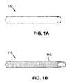
- FIG. 1Ais a diagram of a single crystal semiconductor nanowire.
- FIG. 1Bis a diagram of a nanowire doped according to a core-shell structure.
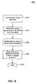
- FIG. 2is a flowchart of a method for preparing nanowires using a combination of Si precursors, according to an embodiment of the invention.
- FIG. 3is a flowchart of a method for preparing nanowires using a combination of Si precursors, according to an embodiment of the invention.
- FIG. 4is a flowchart of a method for nanowire synthesis, according to an embodiment of the invention.
- FIG. 4Ais a diagram of a nanowire synthesis vessel, according to an embodiment of the invention.
- FIG. 5is a flowchart of a method for doping nanowires, according to an embodiment of the invention.
- FIG. 6is a flowchart of a method for reducing surface states from dangling bonds on a nanowire structure, according to an embodiment of the invention.
- FIG. 7is a diagram of a nanowire coated with a sacrificial layer, according to an embodiment of the invention.
- FIG. 8is a diagram showing nanowire processing in accordance with one embodiment of the present invention.
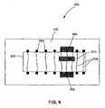
- FIG. 9is a diagram showing nanowire processing following transfer in accordance with one embodiment of the present invention.
- FIG. 10is a flowchart of a method of harvesting a nanowire using a sacrificial portion, according to an embodiment of the invention.
- FIG. 11is a diagram of a nanowire with a sacrificial portion, according to an embodiment of the invention.
- FIG. 12is a flowchart of a method of harvesting a nanowire by monitoring of a PN junction, according to an embodiment of the invention.
- FIG. 13is a flowchart of a method of harvesting a nanowire using a sacrificial metal layer on a nanowire growth substrate, according to an embodiment of the invention.
- FIG. 14is a diagram of a nanowire grown on a sacrificial metal layer on a nanowire growth substrate, according to an embodiment of the invention.
- FIG. 15is a flowchart of a method of harvesting an Si nanowire when using a non-Si substrate, according to an embodiment of the invention.
- FIG. 16is a flowchart of a method of harvesting a nanowire with one orientation when a nanowire growth substrate with a different orientation is used, according to an embodiment of the invention.
- FIG. 17is a diagram of a nanowire with one orientation growing on a nanowire growth substrate with a different orientation, according to an embodiment of the invention.
- FIG. 18is a flowchart of a method for transferring nanowires from a first substrate to a second substrate, according to an embodiment of the invention.
- FIG. 19is a flowchart of a method for transferring nanowires from a first substrate with a patterned coating to a second substrate, according to an embodiment of the invention.
- FIG. 20Ais a diagram of a first substrate with nanowires and a transfer substrate, according to an embodiment of the invention.
- FIG. 20Bis a diagram of a device substrate and a transfer substrate transferring nanowires, according to an embodiment of the invention.
- FIG. 21is a representation of probe nanowire transfer scheme in accordance with one embodiment of the present invention.
- FIG. 22is a representation of global nanowire transfer in accordance with one embodiment of the present invention.
- FIG. 23Ais a transmission electron micrograft that shows a substrate with e-field oriented nanowires prior to transfer, according to an embodiment of the invention.
- FIG. 23Bis a transmission electron micrograft that shows nanowires remaining on substrate following transfer, according to an embodiment of the invention.
- FIG. 23Cis a transmission electron micrograft that shows nanowires on transfer substrate following transfer, according to an embodiment of the invention.
- nanowiresare frequently referred to, the techniques described herein are also applicable to other nanostructures, such as nanorods, nanotubes, nanotetrapods, nanoribbons and/or combinations thereof. It should further be appreciated that the manufacturing techniques described herein could be used to create any semiconductor device type, and other electronic component types. Further, the techniques would be suitable for application in electrical systems, optical systems, consumer electronics, industrial electronics, wireless systems, space applications, or any other application.
- an “aspect ratio”is the length of a first axis of a nanostructure divided by the average of the lengths of the second and third axes of the nanostructure, where the second and third axes are the two axes whose lengths are most nearly equal to each other.
- the aspect ratio for a perfect rodwould be the length of its long axis divided by the diameter of a cross-section perpendicular to (normal to) the long axis.
- heterostructurewhen used with reference to nanostructures refers to nanostructures characterized by at least two different and/or distinguishable material types. Typically, one region of the nanostructure comprises a first material type, while a second region of the nanostructure comprises a second material type.
- the nanostructurecomprises a core of a first material and at least one shell of a second (or third etc.) material, where the different material types are distributed radially about the long axis of a nanowire, a long axis of an arm of a branched nanocrystal, or the center of a nanocrystal, for example.
- a shellneed not completely cover the adjacent materials to be considered a shell or for the nanostructure to be considered a heterostructure.
- a nanocrystal characterized by a core of one material covered with small islands of a second materialis a heterostructure.
- the different material typesare distributed at different locations within the nanostructure.
- material typescan be distributed along the major (long) axis of a nanowire or along a long axis of arm of a branched nanocrystal.
- Different regions within a heterostructurecan comprise entirely different materials, or the different regions can comprise a base material.
- a “nanostructure”is a structure having at least one region or characteristic dimension with a dimension of less than about 500 nm, e.g., less than about 200 nm, less than about 100 nm, less than about 50 nm, or even less than about 20 nm. Typically, the region or characteristic dimension will be along the smallest axis of the structure. Examples of such structures include nanowires, nanorods, nanotubes, branched nanocrystals, nanotetrapods, tripods, bipods, nanocrystals, nanodots, quantum dots, nanoparticles, branched tetrapods (e.g., inorganic dendrimers), and the like.
- Nanostructurescan be substantially homogeneous in material properties, or in certain embodiments can be heterogeneous (e.g., heterostructures). Nanostructures can be, for example, substantially crystalline, substantially monocrystalline, polycrystalline, amorphous, or a combination thereof. In one aspect, each of the three dimensions of the nanostructure has a dimension of less than about 500 nm, for example, less than about 200 nm, less than about 100 nm, less than about 50 nm, or even less than about 20 nm.
- nanowiregenerally refers to any elongated conductive or semiconductive material (or other material described herein) that includes at least one cross sectional dimension that is less than 500 nm, and preferably, less than 100 nm, and has an aspect ratio (length:width) of greater than 10, preferably greater than 50, and more preferably, greater than 100.
- the nanowires of this inventioncan be substantially homogeneous in material properties, or in certain embodiments can be heterogeneous (e.g. nanowire heterostructures).
- the nanowirescan be fabricated from essentially any convenient material or materials, and can be, e.g., substantially crystalline, substantially monocrystalline, polycrystalline, or amorphous.
- Nanowirescan have a variable diameter or can have a substantially uniform diameter, that is, a diameter that shows a variance less than about 20% (e.g., less than about 10%, less than about 5%, or less than about 1%) over the region of greatest variability and over a linear dimension of at least 5 nm (e.g., at least 10 nm, at least 20 nm, or at least 50 nm).
- Nanowires according to this inventioncan expressly exclude carbon nanotubes, and, in certain embodiments, exclude “whiskers” or “nanowhiskers”, particularly whiskers having a diameter greater than 100 nm, or greater than about 200 nm.
- nanowiresexamples include semiconductor nanowires as described in Published International Patent Application Nos. WO 02/17362, WO 02/48701, and WO 01/03208, carbon nanotubes, and other elongated conductive or semiconductive structures of like dimensions, which are incorporated herein by reference.
- nanorodgenerally refers to any elongated conductive or semiconductive material (or other material described herein) similar to a nanowire, but having an aspect ratio (length:width) less than that of a nanowire.
- two or more nanorodscan be coupled together along their longitudinal axis so that the coupled nanorods span all the way between electrodes.
- two or more nanorodscan be substantially aligned along their longitudinal axis, but not coupled together, such that a small gap exists between the ends of the two or more nanorods.
- electronscan flow from one nanorod to another by hopping from one nanorod to another to traverse the small gap.
- the two or more nanorodscan be substantially aligned, such that they form a path by which electrons can travel between electrodes.
- a wide range of types of materials for nanowires, nanorods, nanotubes and nanoribbonscan be used, including semiconductor material selected from, e.g., Si, Ge, Sn, Se, Te, B, C (including diamond), P, B—C, B—P(BP 6 ), B—Si, Si—C, Si—Ge, Si—Sn and Ge—Sn, SiC, BN/BP/BAs, AlN/AlP/AlAs/AlSb, GaN/GaP/GaAs/GaSb, InN/InP/InAs/InSb, ZnO/ZnS/ZnSe/ZnTe, CdS/CdSe/CdTe, HgS/HgSe/HgTe, BeS/BeSe/BeTe/MgS/MgSe, GeS, GeSe, GeTe, SnS, SnSe, SnTe, PbO, PbS,
- the nanowirescan also be formed from other materials such as metals such as gold, nickel, palladium, iradium, cobalt, chromium, aluminum, titanium, tin and the like, metal alloys, polymers, conductive polymers, ceramics, and/or combinations thereof.
- metalssuch as gold, nickel, palladium, iradium, cobalt, chromium, aluminum, titanium, tin and the like
- metal alloyspolymers, conductive polymers, ceramics, and/or combinations thereof.
- Other now known or later developed conducting or semiconductor materialscan be employed.
- the semiconductormay comprise a dopant from a group consisting of: a p-type dopant from Group III of the periodic table; an n-type dopant from Group V of the periodic table; a p-type dopant selected from a group consisting of: B, Al and In; an n-type dopant selected from a group consisting of: P, As and Sb; a p-type dopant from Group II of the periodic table; a p-type dopant selected from a group consisting of: Mg, Zn, Cd and Hg; a p-type dopant from Group IV of the periodic table; a p-type dopant selected from a group consisting of: C and Si.; or an n-type dopant selected from a group consisting of: Si, Ge, Sn, S, Se and Te.
- Other now known or later developed dopant materialscan be employed.
- the nanowires or nanoribbonscan include carbon nanotubes, or nanotubes formed of conductive or semiconductive organic polymer materials, (e.g., pentacene, and transition metal oxides).
- conductive or semiconductive organic polymer materialse.g., pentacene, and transition metal oxides.
- Nanowiree.g., nanowire-like structures having a hollow tube formed axially therethrough.
- Nanotubescan be formed in combinations/thin films of nanotubes as is described herein for nanowires, alone or in combination with nanowires, to provide the properties and advantages described herein.
- FIG. 1Aillustrates a single crystal semiconductor nanowire core (hereafter “nanowire”) 100 .
- FIG. 1Ashows a nanowire 100 that is a uniformly doped single crystal nanowire.
- Such single crystal nanowirescan be doped into either p- or n-type semiconductors in a fairly controlled way.
- Doped nanowires such as nanowire 100exhibit improved electronic properties. For instance, such nanowires can be doped to have carrier mobility levels comparable to bulk single crystal materials.
- FIG. 1Bshows a nanowire 110 doped according to a core-shell structure.
- nanowire 110has a doped surface layer 112 , which can have varying thickness levels, including being only a molecular monolayer on the surface of nanowire 110 .
- the valence band of the insulating shellcan be lower than the valence band of the core for p-type doped wires, or the conduction band of the shell can be higher than the core for n-type doped wires.
- the core nanostructurecan be made from any metallic or semiconductor material, and the shell can be made from the same or a different material.
- the first core materialcan comprise a first semiconductor selected from the group consisting of: a Group II-VI semiconductor, a Group III-V semiconductor, a Group IV semiconductor, and an alloy thereof.
- the second material of the shellcan comprise a second semiconductor, the same as or different from the first semiconductor, e.g., selected from the group consisting of: a Group II-VI semiconductor, a Group III-V semiconductor, a Group IV semiconductor, and an alloy thereof.
- Example semiconductorsinclude, but are not limited to, CdSe, CdTe, InP, InAs, CdS, ZnS, ZnSe, ZnTe, HgTe, GaN, GaP, GaAs, GaSb, InSb, Si, Ge, AlAs, AlSb, PbSe, PbS, and PbTe.
- metallic materialssuch as gold, chromium, tin, nickel, aluminum etc. and alloys thereof can be used as the core material, and the metallic core can be overcoated with an appropriate shell material such as silicon dioxide or other insulating materials.
- Nanostructurescan be fabricated and their size can be controlled by any of a number of convenient methods that can be adapted to different materials. For example, synthesis of nanocrystals of various composition is described in, e.g., Peng et al. (2000) “Shape Control of CdSe Nanocrystals” Nature 404, 59-61; Puntes et al. (2001) “Colloidal nanocrystal shape and size control: The case of cobalt” Science 291, 2115-2117; U.S. Pat. No. 6,306,736 to Alivisatos et al. (Oct. 23, 2001) entitled “Process for forming shaped group III-V semiconductor nanocrystals, and product formed using process”; U.S.
- nanowires having various aspect ratiosincluding nanowires with controlled diameters, is described in, e.g., Gudiksen et al (2000) “Diameter-selective synthesis of semiconductor nanowires” J. Am. Chem. Soc. 122, 8801-8802; Cui et al. (2001) “Diameter-controlled synthesis of single-crystal silicon nanowires” Appl. Phys. Lett. 78, 2214-2216; Gudiksen et al. (2001) “Synthetic control of the diameter and length of single crystal semiconductor nanowires” J. Phys. Chem. B 105, 4062-4064; Morales et al.
- branched nanowirese.g., nanotetrapods, tripods, bipods, and branched tetrapods
- FIG. 1“Controlled synthesis of multi-armed CdS nanorod architectures using monosurfactant system” J. Am. Chem. Soc. 123, 5150-5151; and Manna et al. (2000) “ Synthesis of Soluble and Processable Rod -, Arrow -, Teardrop -, and Tetrapod - Shaped CdSe Nanocrystals” J. Am. Chem. Soc. 122, 12700-12706.
- core-shell nanostructure heterostructuresnamely nanocrystal and nanowire (e.g., nanorod) core-shell heterostructures
- core-shell nanostructure heterostructuresnamely nanocrystal and nanowire (e.g., nanorod) core-shell heterostructures
- Peng et al.1997) “Epitaxial growth of highly luminescent CdSe/CdS core/shell nanocrystals with photostability and electronic accessibility” J. Am. Chem. Soc. 119, 7019-7029; Dabbousi et al. (1997) “(CdSe)ZnS core-shell quantum dots: Synthesis and characterization of a size series of highly luminescent nanocrysallites” J. Phys. Chem. B 101, 9463-9475; Manna et al.
- Nanowire heterostructuresin which the different materials are distributed at different locations along the long axis of the nanowire is described in, e.g., Gudiksen et al. (2002) “Growth of nanowire superlattice structures for nanoscale photonics and electronics” Nature 415, 617-620; Bjork et al. (2002) “One-dimensional steeplechase for electrons realized” Nano Letters 2, 86-90; Wu et al. (2002) “Block-by-block growth of single-crystalline Si/SiGe superlattice nanowires” Nano Letters 2, 83-86; and U.S. patent application 60/370,095 (Apr. 2, 2002) to Empedocles entitled “Nanowire heterostructures for encoding information.” Similar approaches can be applied to growth of other heterostructures.
- FIG. 2is a flowchart of method 200 for preparing nanowires using a combination of Si precursors, according to an embodiment of the invention.
- Method 200begins in step 202 .
- one or more nucleating particlessuitably metal catalysts, are deposited on a substrate material to create a nucleation site for nanowire growth.
- step 208heating the alloy droplet to a second temperature and contacting the alloy droplet with a second precursor gas mixture, allows nanowires to grow at the site of the alloy droplet, which is indicated by label 210 , until they reach the desired size and orientation, as shown in step 214 .
- the substrate material on which the nanowires are grownis a crystallographic substrate.
- crystallographic substrateincludes any substrate material which comprises atoms situated in a repeating or periodic array over large atomic distances, typically on the order of 10 or more angstroms ( ⁇ ). Such crystallographic substrates may be polycrystalline or may comprise single crystals.
- the crystallographic substrate utilized in the processes of the present inventionis silicon (Si).
- the substrate materialmay comprise an amorphous material. Suitable amorphous substrate materials which may be used in the practice of the present invention include, but are not limited to SiO 2 , Si 3 N 4 and alumina.
- the methods of the present inventioncomprise first depositing nucleating particles on a substrate material.
- Nucleating particles that may be used in the practice of the present inventioninclude metal catalysts and can be any metal that reacts with both the first precursor gas mixture and the second precursor gas mixture to form a eutectic phase. Such a mixture has a minimum melting point at which all components are in solution.
- precursor gas moleculese.g., silicon
- a saturation point on the eutectic phase diagramis reached such that semiconductor particles (e.g., Si) begin to precipitate out of the metal solution, thereby creating a growing nanowire.
- Continuous addition of precursor gaswill continue to saturate the eutectic, thereby generating additional material for nanowire growth.
- the nucleating particleswill be metal catalysts and can comprise any of the transition metals from the Periodic Table, including, but not limited to, copper, silver, gold, nickel, palladium, platinum, cobalt, rhodium, iridium, iron, ruthenium, tin, osmium, manganese, chromium, molybdenum, tungsten, vanadium, niobium, tantalum, titanium, zirconium and gallium, including mixtures of one or more of these metals.
- the metal catalystcan comprise a gold (Au) colloid (i.e., a Au nanoparticle) or Au film.
- 60 nanometer (nm) diameter gold colloidscan be used.
- the targetis to achieve a uniform deposition of gold nanoparticles with density between 2-4 particles per square micrometer ( ⁇ m).
- a keyis minimized gold particle cluster formation.
- the clusterscan result in undesired larger diameter nanowire growth.
- Spin coating and self assembly methodscan be explored for the deposition (see e.g., U.S. patent application Ser. No. 10/674,060, filed Sep. 30, 2003, which incorporated by reference herein in its entirety).
- Spin coatingis a fairly straightforward process.
- a deposition densitycan be controlled through variation of the gold particle concentration in the precursor colloids, manipulation of surface chemistry of the silicon wafer, and changing the spin speed.
- a drawback of spin coatingcan be low utilization efficiency of gold colloid solution.
- a recycling process in the production stagecan be used if warranted.
- Self assemblyinvolves some use of well established chemistry.
- the surface of 4 inch silicon oxide coated waferis functionalized with either (3-aminopropyl)-trimethoxysilane (APTMS) or (3-mercaptopropyl)-trimethoxysilane (MPTMS), then contacted with 60 nm gold colloid solution.
- the gold particlesare assembled on the surface. The difference between two different chemistries are compared, and the possibility of controlling the density of gold particles by control of the contact time and gold particle concentration in the contact solution can be used.
- the nucleating particles used to practice the present inventioncan also be formed on a substrate surface by heating a gold film coating layer on the surface.
- the present inventioncomprises heating the first precursor gas mixture to a temperature at which 1) the gas dissociates into its free component atoms, and 2) the nucleating particles (e.g. metal catalyst) melts to a liquid.
- the free gas moleculescan then diffuse into the metal catalyst to form a liquid alloy droplet.
- CVDchemical vapor deposition
- the first precursor gasmay comprise a gas which includes at least one atomic species that promotes the growth of nanowires (e.g., Si) as well as an atomic species that aids in orienting the nanowires during their growth (e.g., Cl atoms).
- the first precursor gasmay be selected from, but not limited to, Si 2 H 6 , SiH 4 , SiCl 4 and SiH 2 Cl 2 gas, preferably SiCl 4 or SiH 2 Cl 2 .
- Si—H bond93 kcal/mole
- Si—Cl bond110 kcal/mole
- Si—Si bond77 kcal/mole
- Dissociation temperatures for SiH 4 and Si 2 H 6 , and SiCl 4 and SiH 2 Cl 2 gasesare between about 300° C.
- the loss of metal catalystis more likely to occur due to increased melting of the catalyst leaving less catalyst (or none) available to promote growth of the nanowires, thus limiting the length to which the nanowires can be grown. Accordingly, following the initiation of nanowire growth and orientation with SiCl 4 or SiH 2 Cl 2 , it is preferable to introduce another precursor gas mixture (including, e.g., Si 2 H 6 or SiH 4 ) to contact the metal catalyst, which gas mixture includes a precursor gas which decomposes into Si atoms at lower temperatures than the first precursor gas (but at a high enough temperature to form a eutectic phase with the metal catalyst).
- another precursor gas mixtureincluding, e.g., Si 2 H 6 or SiH 4
- the precursor gas mixtures used during any of the nanowire growth processesmay further comprise one or more doping gases.
- suitable doping gasesinclude, but are not limited to, B 2 H 6 , POCl 3 and PH 3 .
- the first precursor gascan comprise SiCl 4 and suitably a carrier gas, such as He, Ar, or other inert gas. Heating this gas mixture to a sufficiently high temperature, e.g., above about 800° C., generates free Si and Cl atoms.
- the first precursor gasmay comprise one or more dopant gases selected from those described throughout the application.
- the first precursor gas mixtureis passed over the nucleating particles, suitably metal-catalyst particles (e.g., gold nanoparticles) deposited on the substrate material at a total pressure between about 20 to about 50 Torr, while the nucleating particles are heated up to a temperature of about 80° C.
- the gas pressuremay be increased or decreased, thereby requiring a modification in the temperature required to dissociate the precursor gas mixture.
- SiCl 4when heated to the appropriate temperature will decompose into free Si and Cl atoms.
- B 2 H 6is present in the precursor gas mixture, B atoms will also be generated. Si and B will diffuse into the metal catalyst and generate a liquid alloy droplet. This eutectic phase of metal catalyst and precursor gases will continue to exist as precursor gas is solvated in the metal catalyst. Once an over-saturation is reached, Si/B atoms will precipitate out and initiate nanowire growth. In order to continue nanowire growth, a continuous supply of Si precursor gas and doping gas are required. However, maintaining a temperature above about 800° C. for extended periods can lead to the metal catalyst diffusing into the growing nanowire creating trap states and reducing the diameter and length of the overall nanowire that can be obtained.
- nanowire growthcan be initiated (e.g., using SiCl 4 or SiH 2 Cl 2 ) once nanowire growth is initiated (e.g., using SiCl 4 or SiH 2 Cl 2 ).
- a second precursor gascan be substituted (e.g., SiH 4 ) and nanowire growth continued.
- the point at which the second precursor gas is introduced into the systemcan be determined experimentally by the skilled artisan.
- nanowire growthcan be initiated using SiH 4 and then followed with SiCl 4 or SiH 2 Cl 2 as a second precursor gas thereby allowing for Cl etching.
- the first temperature at which the first precursor gas mixture is added to initiate nanowire growth and the second temperature at which nanowire growth is continued using a second precursor gas mixturecan be the same, so long as the temperature used is high enough to allow for dissociation of the gases and diffusion of Si and dopant into the liquid metal catalyst.
- the first temperature used to initiate nanowire growthwill be higher than the second temperature used to continue nanowire growth.
- These temperaturescan differ by any amount (e.g., about a few degrees C. to 10's of degrees C. to 100's of degrees C.), so long as the temperatures used are high enough to allow for dissociation of the gases and diffusion of Si and dopant into the liquid metal catalyst.
- a second precursor gascan be substituted and the temperature changed to continue nanowire growth.
- the point at which the second precursor gas is introduced into the systemcan be determined experimentally by the skilled artisan.
- the first temperature at which nanowire growth is initiatedwill be higher than the second temperature, where nanowire growth continues.
- the second precursor gaswill comprise SiH 4 and growth will continue at a temperature of about 300° C. to about 500° C.
- the first temperaturewill be at least about 50° C. above the second temperature.
- nanowire growthcan be initiated with a first precursor gas comprising SiCl 4 , suitably at a temperature of about 800° C., and then continued with a second precursor gas comprising SiH 2 Cl 2 , suitably at a temperature of about 750° C.
- SiH 2 Cl 2can be used as the first precursor gas.
- the wiresthen can be contacted with a third precursor gas, comprising, for example SiH 4 or Si 2 H 6 , suitably at a temperature of about 300-500° C. As shown in FIG.
- any number of precursor gasescan be introduced to the nanowires during the initiation and growth processes, until the nanowires reach the desired size and orientation, which is indicated in step 214 .
- the wireswill continue to grow, as Si (or other suitable semiconductor materials as discussed throughout) and the dopant will continue to precipitate out of the metal catalyst allow droplet.
- nanowire growthcan be initiated using SiH 4 or Si 2 H 6 and then continued using SiCl 4 or SiH 2 Cl 2 to allow for Cl etching of Si growing in undesired locations and orientations on the substrate surface.
- the precursor gas mixturemay then be switched back to SiH 4 or Si 2 H 6 if desired.
- the temperature at which the three gasescan be kept the same, or can be modified as needed, so long as free Si atoms are allowed to mix with the liquefied metal catalyst.
- free Si, Cl or H atomsmay be supplied to the growing nanowires to aid in growth (e.g., Si), etching (e.g., Cl) or gas dissociation (e.g., H) as needed.
- growthe.g., Si
- etchinge.g., Cl
- gas dissociatione.g., H
- the precursor gas mixtures used in the processes of the present inventionmay further comprise a dopant.
- wirescan be grown using the same doping gas in each of the precursor gas mixtures. In such embodiments, the entire resulting wire will be either p-type or n-type, depending on the choice of dopant.
- different doping gasescan be introduced throughout the process as components of the different precursor gases. For example, wire growth can be initiated using a precursor gas comprising a n-type dopant (e.g., P, As or Sb) and then continued using a precursor gas using a p-type dopant (e.g., B, Al or In). In other embodiments, a p-type doing gas will be used during initiation and then an n-type doping gas during growth.
- a precursor gas comprising a n-type dopante.g., P, As or Sb
- a p-type dopante.g., B, Al or In
- the type of doping gascan be switched multiple times throughout the growth process as the precursor gases are switched.
- the resulting nanowirestherefore can comprise several different dopant portions throughout their length.
- a nanowire produced via the present inventionmay comprise an n-type base, a p-type middle section, and an n-type top, or any suitable combination as envisioned by the ordinarily skilled artisan.
- Such embodiments of the present inventionwould allow for an n-type wire to be grown on a p-type substrate, and vice versa.
- the nanowirewill allow the nanowire to continue growing until termination by desire or death caused by local condition change.
- the quality of the nanowiresis dependent on the quality of gold nanoparticles, control of gold nanoparticle distribution on the substrate and growth condition including temperature, ratio of dopant to precursor gas, partial pressure of the precursor gas, and resident time of precursor gases in the reactor.
- the processes of the present inventioncan be accomplished using a computer controlled 8′′ semiconductor furnace.
- the various precursor gas mixtures that are introduced in any of the processes of the present inventionmay be introduced via Plasma Enhanced Sputter Deposition (or Plasma Enhanced Chemical Vapor Deposition (PECVD)) and the processes performed at lower temperatures.
- PECVDPlasma Enhanced Chemical Vapor Deposition
- a carrier gase.g., H 2 , H 2 Ar
- Chlorineaids in removal of interfacial oxide on Si substrates leading to the oriented NW growth.
- Loss of metal catalyste.g., Au
- Sputter depositioncan be accomplished via any method known to the ordinarily skilled artisan, for example, diode, radio frequency and direct current deposition.
- the diameter distribution of silicon nanowires of these certain embodiments of the present inventionis determined by that of the nucleating particles, e.g., metal (suitably gold) nanoparticles.
- the nucleating particlese.g., metal (suitably gold) nanoparticles.
- metal (suitably gold) nanoparticlescan have a diameter distribution of ⁇ 10%. The same distribution can be attained in the nanowires.
- Gold nanoparticlescan be split into smaller ones resulting in smaller diameter nanowires, depending on the growth condition. Growth conditions can be optimized to minimize this event. Given a growth condition, the length of nanowires can be controlled by varying duration of the growth. Crystallinity of silicon nanowires and dopant concentration are also growth condition dependent. They can be optimized and controlled together with other important nanowire characteristics.
- the nanowires produced according to any of the processes of the present inventionwill suitably grow out of the plane of the substrate material.
- Such growthincludes nanowires that project out of the plane of the substrate material at any angle with respect to the substrate.
- nanowirescan grow at an angle of about 1° to about 90°, and any angle in between these values, relative to the plane of the substrate material.
- the nanowires produced by the processes described hereinmust project out of the plane of the substrate. That is, the nanowires produced by the processes of the present invention must extend off of the plane of the substrate material a distance greater than the dimension of a single molecule.
- the nanowires produced according to the present inventionare distinct from structures such as thin films and quantum dots, which spread on the surface of a substrate material, rather than growing in a manner such that they project out of the plane of the substrate a distance that exceeds the atomic diameter of a single Si molecule for instance.
- the nanowires produced according to any of the processes of the present inventionwill project out of the plane of the substrate material so as to attain a final length of about 100 nm to less than about 1 ⁇ m.
- the nanowires produced according the present inventioncan attain a final length of a few 100 nms.
- the nanowires of the present inventionwill suitably be at least about 1 nm to less than about 1 ⁇ m in diameter.
- the nanowires of the present inventionwill have a diameter of about a few nms to 100's of nms, so as to allow them to be harvested and utilized in an electronic device, suitably by placing the wires in plastic substrates so as to act as conductive media. (See U.S. Application No. 60/491,979, filed Aug. 4, 2003, for a description of nanowire harvesting which is incorporated herein by reference.)
- the nanowireswhen growing on a crystalline substrate (whether polycrystalline or single crystal) will preferably grow in an epitaxial orientation.
- the present inventionalso embodies growth on crystalline substrates wherein the nanowires do not grow in an epitaxial orientation.
- the term epitaxial as it refers to the growth of nanowiresmeans that the nanowires have the same crystallographic characteristic(s) as the substrate material on which they are growing.
- the orientation of the substrate materialcan be any crystallographic orientation known to the ordinarily skilled artisan, including, but not limited to, ⁇ 111>, ⁇ 110>, ⁇ 100> and ⁇ 211>.
- the nanowires produced by the processes of the present inventioncan be grown in any crystallographic orientation, and suitably in the same orientation as the substrate material, including those orientations discussed throughout and as known to the ordinarily skilled artisan.
- the crystallographic plane of the substrate materialcan be off axis of the 0° horizontal plane.
- the nanowires growing on the surface of such a substrate materialcan project out of the substrate material at an angle such that the wires can be normal to the crystallographic plane (i.e., 90° with respect to the crystallographic plane) or can be off axis relative to the crystallographic plane such that they can be normal to a 0° horizontal plane.
- the nanowires produced according to the processes of the present inventionwill not grow epitaxially, as the amorphous material does not comprise a crystallographic orientation.
- the nanowires grown on such substratesmay project out of the plane of the substrate at any angle relative to the horizontal plane.
- the processes of the present inventionproduce nanowires that may carry electrons between two points in space and thus act to transfer charge.
- the nanowires of the present inventionare further distinct from nanodots and in their size and orientation, are distinct from semiconductor films.
- FIG. 3is a flowchart of a method for preparing nanowires using a combination of Si precursors which does not require a starting metal catalyst, according to an embodiment of the invention.
- Method 300begins in step 302 .
- a substrate materialis hydroxylated to produce nucleation sites.
- contacting the substrate material with a first precursor gas mixturegenerates one or more nuclei on a surface of the substrate material, which is indicated by label 306 .
- contacting the nuclei with a second precursor gas mixtureallows nanowires to grow at the site of the one or more nuclei, as indicated by label 310 , until they reach the desired size and orientation, which is shown as step 314 .
- This process of the present inventiondoes not require the use of a metal catalyst to provide a nucleation site for the nanowire, and therefore eliminates the problems and concerns that arise due to metals diffusing into the growing nanowires.
- a similar processhas been described by De Salvo et al. for the production of nanocrystals in the form of nanodots (“How far will Silicon nanocrystals push the scaling limits of NVMs technologies?,” IEEE Proceeding, Session 26, p. 1 (2003)), but has not been extended to the production of nanowires as in the present invention.
- any suitable substrate materialmay be used for the processes of the present invention.
- the substrate materialwill be crystallographic, including both polycrystalline and single crystal substrates.
- the substrate material utilized in this embodiment of the present inventionwill comprise silicon.
- the substrate materialwill be an amorphous material, including but not limited to, SiO 2 , Si 3 N 4 , or alumina.
- Hydroxylation of the substrate material in these embodiments of the present inventioncan be generated by any suitable process known to the ordinarily skilled artisan.
- hydroxylation of a substrate material of the present inventioncan be generated by chemical treatment of the substrate material with diluted HF solution.
- Generation of hydroxyl groups on the surface of the substrate materialcreate nucleation points for Si or other semiconductor materials to deposit and initiate nanowire growth.
- the substrate materialis then contacted with one or more precursor gas mixtures to allow nucleation and initiation of nanowire growth.
- Any precursor gas mixture known to the ordinarily skilled artisancan be used in the processes of the present invention, and suitably can comprise dopants.
- precursor gases useful in the practice of the present inventioncomprise, but are not limited to, SiH 4 , Si 2 H 6 , SiCl 4 and SiH 2 Cl 2 , preferably SiH 4 or Si 2 H 6 , which nucleates particles on the surface of the substrate, and in suitable embodiments may further comprise dopants such as, but not limited to, B 2 H 6 , POCl 3 and PH 3 .
- the temperature for dissociation and nucleation of the nanowiresis dependent upon the dissociation temperature of the precursor gas mixture as discussed throughout. In suitable embodiments, this temperature is at least about 300° C., but is optimized based on the dissociation temperature of the precursor gas mixture as discussed throughout. In certain such embodiments, the first precursor gas mixture will comprise SiH 4 .
- the substrate materialis then contacted with one or more second precursor gas mixtures as described throughout, and suitably can comprise SiH 4 , Si 2 H 6 , SiCl 4 or SiH 2 Cl 2 , preferably SiCl 4 or SiH 2 Cl 2 , and may comprise B 2 H 6 , POCl 3 or PH 3 .
- the second precursor gas mixturewill comprise SiCl 4 or SiH 2 Cl 2 . Use of such precursor gases will allow for growth in a ⁇ 111> orientation when grown on a crystallographic substrate as a result of etching from the dissociated Cl as discussed above.
- any number of precursor gasesmay be introduced to the nanowires during the initiation and growth processes, as long as one or more of the precursor gases is capable of nucleating particles on the surface of the substrate, and one or more precursor gas(es) aids in orienting the nanowires during the growth process (e.g., via etching).
- the wireswill continue to grow.
- free H, Cl or Si atomscan be added to the growing nanowires as discussed throughout.
- the processes of the present inventioncan be used to produce nanowires that comprise various dopants and different regions of these dopants throughout the length of the nanowire.
- the nanowires producedwill preferably grow in an epitaxial orientation, though the present invention also encompasses embodiments where growth on crystallographic substrates is not epitaxial.
- the processes of the present inventionas discussed throughout, produce nanowires that grow and project out of the plane of the substrate material.
- the nanowires of the present inventionare distinct from nanodots that do not grow in such an orientation, but rather remain in the plane of the substrate material.
- the present inventionby providing Si structures that project out of the plane of the substrate material, allow for the production of nanowires that can be used to transport electrical charge as discussed throughout.
- a method for producing nanowiresincludes hydroxylating a substrate material; contacting the substrate material with a first precursor gas mixture comprising a first precursor gas that is capable of forming one or more nucleated particles on a surface of the substrate material; contacting the one or more nucleated particles with a second precursor gas mixture, comprising at least one atomic species that aids in orienting the growing nanowires; and growing nanowires at the site of the one or more nucleated particles.
- the first precursor gas mixturecomprises SiH 4 or Si 2 H 6 .
- the second precursor gas mixturecomprises SiCl 4 or SiH 2 Cl 2 .
- the second precursor gas mixturecomprises chlorine gas from an independent chlorine gas source which is separate from the source of SiCl 4 or SiH 2 Cl 2 gas. Nanowires can be produced by this method. Electronic circuits including nanowires produced by this method can also be produced.
- nanowires produced by any of the processes of the present inventionwill suitably be of a length of at least about 100 nm and at least about 1 nm to less than about 1 ⁇ m in diameter, and may comprise various dopants (i.e., p- and n-type regions) throughout their length.
- the present inventionalso provides for electronic circuits comprising the nanowires produced by any of the processes of the present invention.
- Suitably collections of nanowires produced according to the processes of the present inventionare useful building blocks for high performance electronics.
- a collection of nanowires orientated in substantially the same directionwill have a high mobility value.
- nanowirescan be flexibly processed in solution to allow for inexpensive manufacture. Collections of nanowires can be easily assembled onto any type of substrate from solution to achieve a thin film of nanowires.
- a thin film of nanowires used in a semiconductor devicecan be formed to include 2, 5, 10, 100, and any other number of nanowires between or greater than these amounts, for use in high performance electronics.
- Nanowires of the present inventioncan also be used to make high performance composite materials when combined with polymers/materials such as organic semiconductor materials, which can be flexibly spin-cast on any type of substrate.
- Nanowire/polymer compositescan provide properties superior to a pure polymer materials. Further detail on nanowire/polymer composites is provided below.
- Collections or thin films of nanowires of the present inventioncan be aligned into being substantially parallel to each other, or can be left non-aligned or random.
- Non-aligned collections or thin films of nanowiresprovide electronic properties comparable or superior to polysilicon materials, which typically have mobility values in the range of 1-10 cm 2 /V ⁇ s.
- Aligned thin films of nanowires of the present inventioncan be obtained in a variety of ways.
- aligned thin films of nanowirescan be produced by using the following techniques: (a) Langmuir-Blodgett film alignment; (b) fluidic flow approaches, such as described in U.S. Ser. No. 10/239,000, filed Sep. 10, 2002, and incorporated herein by reference in its entirety; and (c) application of mechanical shear force.
- mechanical shear forcecan be used by placing the nanowires between first and second surfaces, and then moving the first and second surfaces in opposite directions to align the nanowires.
- Aligned thin films of nanowires/polymer compositescan be obtained using these techniques, followed by a spin-casting of the desired polymer onto the created thin film of nanowires.
- nanowirescan be deposited in a liquid polymer solution, alignment can then be performed according to one of these or other alignment processes, and the aligned nanowires can then be cured (e.g., UV cured, crosslinked, etc.).
- An aligned thin film of nanowires/polymer compositecan also be obtained by mechanically stretching a randomly oriented thin film of nanowires/polymer composite.
- P-doped nanowires and n-doped nanowires produced by the processes of the present inventioncan be separately fabricated, and deposited in a homogeneous mixture onto a surface, such as a macroelectronic substrate. On a macroscopic level, the resulting material appears to contain a high concentration of both n- and p-dopants.
- macroelectronic devicescan be fabricated that respond as if they are both n- and p-doped.
- a resulting thin film of nanowires that includes both n-doped and p-doped nanowirescan exhibit characteristics of both n-doped and p-doped nanowires.
- diode, transistor, and other known electrical devicescan be fabricated to include a combination of p-doped nanowires and n-doped nanowires.
- Nanowires produced by the processes of the present inventioncan also be used to produce electrical devices such as p-n diodes, transistors, and other electrical device types, using nanowire heterostructures as described herein.
- Nanowire heterostructuresinclude a plurality of p-n junctions along the length of the nanowire and can include alternating portions or segments along their lengths that are differently doped.
- FIG. 4is a flowchart of method 400 for nanowire synthesis, according to an embodiment of the invention.
- Method 400provides a method for synthesis of nanowires using synthesis vessel 455 , as illustrated in FIG. 4A .
- synthesis vessel 455is a sealed quartz tube.
- Synthesis vessel 455can be, but is not limited to, tubes, pipettes, and the like.
- the dimensions of synthesis vessel 455can be varied to meet the particular production needs of the user. In research scale operation, the dimensions for synthesis vessel 455 typically range from six to eighteen inches in length and one-half inch to one inch in diameter.
- Method 400begins in step 410 .
- a granular precursor materialis position at one end of a synthesis vessel, which is at temperature T 1 .
- precursor material 470is positioned at end 460 of synthesis vessel 455 .
- Example granular precursor materialscan include, but are not limited to Si, CdS and GaN.
- T 1will be a function of the type of granular precursor material. For example, if the granular precursor material is CdS, then T 1 can be in the range from about 800 to 950 degrees centigrade. In this example, T 2 would be approximately 50 degrees centigrade less than T 1 with some variance based on the type of transport mechanism and transport agent, as would be known by individuals skilled in the relevant arts based on the teachings herein.
- catalyst particles supported by a substrateare positioned at the other end of a synthesis vessel, which is at temperature T 2 .
- catalyst particles supported by substrate 470are positioned at end 465 of synthesis vessel 455 .
- catalyst particlescan include Au when Si is used as the granular precursor material, and Ni when GaN is used as the granular precursor materials.
- step 430materials are transported from one end of the synthesis vessel to the other.
- thermal vaporizationis used to transport the granular precursor materials, such as granular precursor materials 470 to the other end of the vessel.
- a chemical vapor transport agentcan be used to transport the granular precursor material.
- Chemical vapor transport agentscan include, but are not limited to chlorine, iodine, and bromine.
- a transfer agentis reacted with the granular precursor materials to form nanowires.
- the transfer agentreacts with granular precursor materials at T 1 to form a volatile compound, which will diffuse to the surface of catalyst particles and decompose to grow nanowires at T 2 .
- the transport agentis regenerated and ready for another cycle to produce more nanowires. The growth cycle will continue until the process is terminated.
- FIG. 5is a flowchart of method 500 for doping nanowires, according to an embodiment of the invention.
- Method 500is similar to method 400 , except that instead of synthesizing nanowires as was done in method 400 a similar approach to that of method 400 is used to dope nanowires.
- Method 500begins in step 510 .
- a dopant precursor materialis positioned at one end of a synthesis vessel, which is at temperature T 1 .
- Example dopant precursor materialscan include, but are not limited to Mg, B, and PO 4 .
- nanowiresare positioned at the other end of a synthesis vessel, which is at temperature T 2 .
- Example nanowirescan include, but are not limited to GaN nanowires and Si nanowires.
- materialsare transported from one end of the synthesis vessel to the other.
- thermal vaporizationis used to transport the dopant precursor materials to the other end of the vessel.
- a chemical vapor transport agentcan be used to transport the dopant precursor material.
- Chemical vapor transport agentscan include, but are not limited to, chlorine and bromine. When phosphates are used as the precursor dopant material, the phosphate can also serve as the chemical vapor transport agent.
- step 540the transfer agent is reacted with the granular precursor materials to form nanowires.
- the transfer agentreacts with granular precursor materials at T 1 to form a volatile compound, which will diffuse to the surface of the nanowires and decompose to grow nanowires at T 2 .
- the transport agentis regenerated and ready for another cycle to dope more nanowires. The growth cycle will continue until the process is terminated.
- the above methodcan be summarized as a method for doping nanowires, including positioning a granular dopant precursor material at one end of a vessel at a first temperature; positioning nanowires at an opposite end of the vessel at a second temperature; transporting granular dopant precursor materials from one end of the vessel to the other end of the vessel; and reacting granular dopant precursor material with nanowires to form doped nanowires.
- Thermal vaporizationcan be used to transport the granular nanowire precursor material.
- a chemical vapor transport agentcan be used to transport the granular nanowire precursor material.
- the chemical vapor transport agentcan be one of chlorine, iodine and bromine.
- the granular dopant precursor materialcan be Mg and the nanowires can be GaN.
- the nanowirescan be Si and the granular dopant precursor material can be B.
- FIG. 6is a flowchart of method 600 to reduce surface states from dangling bonds on a nanowire structure, according to an embodiment of the invention.
- dangling Si bondsoften form at the interface between an Si nanowire and a dielectric that inhibit nanowire performance.
- Hydrogen passivationis often used in Si nanowire processing to reduce surface states from dangling bonds to address this problem.
- the hydrogen plasmacan induce surface damage during processing.
- Method 600describes an approach to use a sacrificial layer to protect the nanowire, while passivation is used to reduce surface states of dangling bonds.
- Method 600begins in step 610 .
- a nanowire structureis created.
- a sacrificial layeris deposited on the nanowire structure.
- FIG. 7is a diagram of a nanowire structure coated with a sacrificial layer, according to an embodiment of the invention.
- the nanowire structureincludes nanowire 710 , dielectric 720 , gate 730 and sacrificial layer 740 .
- Dielectric 720coats nanowire 710
- gate 730coats dielectric 720 .
- Sacrificial layer 740coats gate 730 .
- the entire nanowire structureis formed on substrate 750 .
- the nanowire structurecan include only a nanowire, such as nanowire 710 , which is formed on substrate 750 .
- Sacrificial layer 740can include, but is not limited to SiO 2 or SiN.
- Dielectric 720can include, but is not limited to SiO 2 or SiN.
- Gate 730can include doped amorphous Si, but is not limited to doped amorphous Si.
- substrate 750can include Si, but is not limited to Si.
- the nanowire structure with the sacrificial layeris passivated.
- hydrogen passivationcan be used.
- the sacrificial layeris chemically removed.
- selective etching with a wet etchantcan be used to chemically remove the sacrificial layer, as would be known by individuals skilled in the relevant arts based on the teachings herein. The particular wet etchant to use would be selected based on the particular material contained within the sacrificial layer and the type of nanowire.
- the present inventionprovides processes by which nanowires can be modified directly on a substrate for device preparation.
- the nanowires used in these processeswill be substantially vertical nanowires.
- Vertical nanowiresencompasses nanowires that are substantially perpendicular to the surface of the substrate on which they are grown or deposited.
- the vertical nanowireswill be oriented such that they are between about 45° and about 90° with respect to the horizontal plane of the substrate, more suitably about 60° to about 90°, and most suitably about 80° to about 90° with respect to the horizontal plane of the substrate.
- Such nanowirescan be produced using any suitable nanowire growth process known in the art, including those disclosed herein.
- the substrate materialwill be single-crystalline or polycrystalline, such that growth from the substrate will generate oriented, straight, single crystal dimension wires (suitably epitaxially oriented nanowires).
- the nanowirescan be horizontal, such as disclosed in U.S. Provisional Patent Application No. 60/632,337, filed Dec. 2, 2004, the disclosure of which is incorporated by reference herein in its entirety.
- the nanowiresafter processing of the nanowires on the growth substrate, the nanowires can be removed from the substrate by coating the nanowires with a polymer to form a composite, and then removing the nanowires from the substrate.
- the present inventionprovides processes for producing a nanowire device, comprising: providing a substrate having nanowires attached to a surface in a vertical orientation; depositing a dielectric layer on the surface of the nanowires; depositing one or more nanowire contacts on the nanowires; depositing a material over the nanowires to form a nanowire composite; and separating the nanowire composite from the substrate.
- the nanowire compositecan then be transferred to a second substrate where the nanowires can be metallized.
- any on-substrate processing known or required by those skilled in the artcan be performed on the substantially vertical nanowires.
- a dielectric layercan be grown or deposited directly on the wires.
- the dielectric layercan be formed by oxidizing the nanowires, or otherwise forming the dielectric layer.
- Polymer dielectrics for use in the present inventioninclude for example, polyimides, fluorinated polyimides, polybezimidazoles and others.
- Dielectrics for use in the inventioninclude SiO 2 , Ta 2 O 5 , TiO 2 , ZrO 2 , HfO 2 , Al 2 O 3 , and similar materials.
- Nitride dielectricsinclude AlN and SiN As the wires are substantially separate, each wire can be fully coated with a dielectric material without the concern of sections of overlapping wire not receiving coating.
- further processingcan include oxidation or nitridization of the nanowires.
- Nitridation of nanowirescan be accomplished with processes similar to those employed in oxidation of nanowires. These materials can be applied to nanowires by chemical vapor deposition (CVD), solution phase over-coating, or by spin-coating the appropriate precursor onto the substrate. Other known techniques can be employed, for example sputtering and others.
- an implantsuch as a gate electrode
- an implantsuch as a gate electrode
- Nanowire contactsincluding sources, drains and gates, for example, can be pattered on the substrate using standard photolithography, ink-jet printing, or micro-contact printing processes, for example, or by other processes as described throughout.
- FIG. 8is a diagram showing nanowire processing in accordance with one embodiment of the present invention.
- substantially vertical nanowires 804can have dielectric layers 812 and/or metallic contacts 808 , for example, deposited onto them.
- the nanowirescan then be encapsulated in polymer 806 , thereby producing a composite comprising polymer and nanowires.
- polymer 806By covering all or a portion of the nanowires, composites comprising various densities of nanowires can be produced.
- Vertically grown nanowireswill suitably be of the same overall length, owing to control of growth times and conditions.
- nanowiresmay not be necessary, as the vertical nanowires will already be substantially aligned and oriented when grown, especially when grown from a poly- or single-crystalline substrate 802 .
- Creating a polymeric compositeallows several nanowires to be removed together and subsequently transferred to a second, third, forth, etc. substrate material where metallic contacts can be added or additional processing can take place.
- Suitable polymers for use in forming the nanowire compositesinclude, but are not limited to, elastomers, thermoplastics and thermosetting resins.
- Useful polymersinclude oligomers, which includes, but is not limited to, monomers, dimers, trimers, tetramers, pentamers, hexamers, heptamers, octamers, nonamers, decamers, undecamers, and dodecamers; branched, hyperbranched, dendritic and other non-linear structural forms of polymers; prepolymers such as phenoxy and epoxy prepolymers; networked polymers such as interpenetrating and semi-interpenetrating network polymers; homopolymers, copolymers, terpolymers and other copolymers including random, statistical, alternating, block and graft copolymers and blends of two or more different polymers.
- polymers for use in nanowire compositesinclude, but are not limited to, polyalkanes, polyhaloalkanes, polyalkenes, polyalkynes, polyketones, polycarbonates, polyamides, polyimides, polyarylenes, polyarylvinylenes, polyheteroarylenes, polyheteroarylvinylenes, polyesters, polyethers, polyurethanes, polybenzimidazoles, polysulfides, polysiloxanes, polysulfones, polysaccharides, polypeptides, polyphosphazenes, polyphosphates, phenolic and phenol-formaldehyde resins, epoxy and phenoxy resins, and urea- and melamine-formaldehyde resins.
- Such composites and methods for their preparationare disclosed in U.S.
- the polymer compositewill comprise a mixture of at least two or more different polymers, and in certain embodiments a mixture of at least two epoxy polymers.
- Removal of the polymer-nanowire composite 810 from substrate 802can be achieved via any suitable method, including mechanical separation (e.g., cutting with a blade or tearing the nanowires from the substrate), chemical separation, including wet or dry etching, or chemical-mechanical polishing.
- Suitable etching agentsinclude, but are not limited to KOH, XeF 2 and hydrofluoric acid and can be combined with an oxidizing agent such as HNO 3 or H 2 SO 4 .
- a removable layercan separate the nanowires from the substrate material. After generating the polymer-nanowire composite, the removable layer can be removed.
- the removable layercan be dissolved by a solvent that will dissolve the removable layer, but not dissolve the polymer-nanowire composite or the substrate below the removable layer.
- the removable layercan be a photoremovable layer, in which ultraviolet or other suitable wavelengths of light are used to remove the removable layer, thereby allowing separation of the polymer-nanowire composite from the substrate.
- a photoremovable layeris a substance that breaks down and disintegrates in the presence of ultraviolet light.
- the composite material used to encapsulate the nanowireswill be hardened prior to removing the nanowires from the substrate.
- the compositecan then be transferred to a second substrate where further processing can take place.
- this second substratecan be selected so as to tolerate elevated temperatures, such that doping of the nanowires can take place.
- Methods by which to dope the nanowiresare well known in the art and can be used to dope the nanowires and polymer-nanowire composites of the present invention.
- FIG. 9is a diagram showing nanowire processing following transfer in accordance with one embodiment of the present invention.
- the polymer-nanowire composites 810can subsequently be transferred to an additional substrate 902 where the nanowires can be metallized 904 to form electrical conductivity to device regions (e.g., gain, source, gait).
- nanowires 804can be coupled between a source electrode 906 and a drain electrode 908 over a portion of the gate electrode 910 .
- source and drain electrodescan be added and ohmic contacts can be generated on the wires.
- gate isolation and metal processing stepsas known in the art can be used to finalize the nanowire preparation.
- Such processingallows for wafers that can comprise multiple semiconductor devices on the same base substrate.
- such processingcan occur directly on the growth substrate 802 , followed by removal of the nanowire composite, such that all, or substantially all, nanowire processing is prepared on the initial growth substrate 802 .
- Semiconductor devices prepared according to the present inventioncan have any number of contact areas formed to provide electrical connectivity.
- anode and cathode electrodescan be formed with diodes or other two-terminal devices.
- Other semiconductor devicescan have greater or fewer numbers of contact areas formed.
- Suitable methods of preparing semiconductor devices using the processes and nanowires of the present inventionare disclosed in U.S. patent application Ser. No. 10/674,060, filed Sep. 30, 2003, which is incorporated herein by reference in its entirety.
- a variety of contact area typescan be formed according to the present invention.
- the contact areascan be Ohmic and non-Ohmic.
- a non-Ohmic Schottky diode barrier contactcan be used as an electrode.
- a Schottky diode barrier contactis commonly used for a III-V semiconductor material when it is difficult to make high quality gate dielectrics.
- Source electrodes, gate electrodes, and drain electrodesare formed of a conductive material, such as a metal, alloy, silicide, polysilicon, or the like, including combinations thereof, as would be apparent to a person having ordinary skill in the art. Note that the order in which the gates, sources, and drains are patterned can be varied. For example, gates, sources, and drains can be patterned simultaneously with each other or at different times.
- Suitable metallization schemesinclude Ti—Au, Ni and Al by electron beam (e-beam) evaporation.
- Various further processes, including ion gun cleaning, or HF etchingcan be employed to remove the surface dielectrics prior to metallization of source-drain electrodes.
- a method for producing a nanowire deviceincludes providing a substrate having nanowires attached to a surface in a vertical orientation with respect to the substrate; depositing a dielectric layer on the surface of the nanowires; depositing one or more nanowire contacts on the nanowires; depositing a material over the nanowires to form a nanowire composite; and separating the nanowire composite from the substrate.
- This methodcan further include transferring the nanowire composite to a second substrate.
- This methodcan further include metallizing the nanowires.
- the substratecan be crystalline or polycrystalline.
- the materialcan a polymer, which include an elastomer, thermoplastic or thermosetting resin.
- the materialcan include a mixture of at least two or more different polymers.
- the materialcan include a mixture of at least two epoxy polymers.
- the materialcan be hardened after depositing a material over the nanowires to form a nanowire composite and before separating the nanowire composite from the substrate.
- separating the nanowire composite from the substrateincludes using a blade or chemically etching the nanowire composite from the substrate.
- FIG. 10is a flowchart of method 1000 for harvesting a nanowire using a sacrificial portion, according to an embodiment of the invention.
- Nanowiresare presently grown on substrates using an catalytic colloid to initiate nanowire growth.
- a difficulty limiting the ability to consistently grow and harvest high quality nanowiresis the ability to remove the nanowires from the substrate without incurring physical damage to the wire, such as breakage.
- Current removal methodsinclude using ultrasound and mechanical shearing. However, a problem with each of these is that they cause random breaks in the nanowires resulting in a non-uniform distribution of nanowire lengths.
- Methods 1000 , 1200 , 1300 , 1500 and 1600 provided belowdescribe methods to address this problem.
- method 1000involves the use of a sacrifical portion of a nanowire to provide more effective removal of the nanowires.
- Method 1000begins in step 1010 .
- a desired portion of a nanowireis grown.
- an Au colloidis used to grow the desired portion of the nanowire.
- a sacrificial portion of a nanowireis grown that has different properties from the desired portion.
- FIG. 11illustrates a nanowire with a desired and sacrificial portion of a nanowire, according to an embodiment of the invention.
- FIG. 11shows a nanowire including three parts—sacrificial portion 1110 , desired portion 1120 and stub 1130 , which is described below, that has been grown on substrate 1140 .
- the properties that differcan be that different alloys are used for the sacrificial and desired portions of the nanowire.
- the sacrificial portioncan be SiGe and the desired portion can be Si.
- dopingcan be varied for the sacrificial and desired portion of the nanowire.
- the sacrificial portioncan be n-doped and the desired portion can be p-doped.
- the sacrificial portioncan be p-doped and the desired portion can be n-doped.
- the sacrificial portioncan have no doping, and the desired portion can be either p-doped on n-doped.
- an Au alloycan be used to grow the sacrificial portion of the nanowire.
- the Au alloycan include, but is not limited to AuGe or AuSiGe, when Si nanowires are being grown and harvested.
- the sacrificial portion of the nanowirecan include SiGe and the desired portion can include Si.
- Auwould be used in step 1010 and AuGe would be used in step 1020 to stimulate nanowire growth, for example.
- a boron NWScan be used as a dopant during the growth of the sacrificial portion of the nanowire.
- step 1030the desired portion of the nanowire is protected.
- a photoresistcan be applied to the desired portion of the nanowire to protect the nanowire.
- the desired portion of the nanowireis not protected.
- the sacrificial portion of the nanowireis differentially removed.
- the sacrificial portion of the nanowirecan be differentially removed by using a wet etchant with a etching rate that is significantly higher for the materials within the sacrificial than for the materials within the desired portions of the nanowire.
- a wet etchantwith a etching rate that is significantly higher for the materials within the sacrificial than for the materials within the desired portions of the nanowire.
- hydrofluoric peroxide acetic acid(1 HF: 2 H 2 O 2 : 3 CH 3 COOH) can be used to remove a sacrificial portion that contains SiGe, when the desired portion is Si.
- the etchantremoves the SiGe alloy and stops efficiently at the Si surface of the desired portion.
- Other etchantscan be used, as would be known by persons skilled in the relevant arts based on the teachings herein.
- etchantscan include, by are not limited to potassium hydroxide (KOH), tetramethylammonium hydroxide (TMAH) and ethylene diamine/pyrocatecol/water (EDP). These etchants etch the sacrificial portion of the nanowire at a rate ranging from 27:1 to greater than 500:1 compared to the etch rate of the desired portion, when Si nanowires are used, for example. The range depends on the specific etchant and the temperature, as would be known by individuals skilled in the art.
- step 1050a stub at the tip of the nanowire is removed.
- this stubwill be a residual and undesirable by-product of the catalyst used to initiate nanowire growth. Methods of removal will be known by individuals skilled in the relevant arts.
- step 1060method 1000 ends.
- FIG. 12is a flowchart of method 1200 for harvesting a nanowire while monitoring of a PN junction, according to an embodiment of the invention.
- Method 1200is similar to the embodiment involving different doping levels described with respect to method 1000 . In method 1200 , however, leakage current across a PN junction created between a sacrificial and desired portion of the nanowire is monitored to determine when the sacrificial portion has been successfully etched away.
- Method 1200begins in step 1210 .
- a desired portion of a nanowireis grown.
- a sacrificial portion of the nanowireis grown.
- the desired portionis grown, such that the desired portion is differentially doped from the sacrificial portion.
- the desired portion of the nanowireis protected.
- a photoresistcan be applied to the desired portion of the nanowire.
- the sacrificial portion of the nanowireis differentially etched in a manner similar to that described with respect to step 1040 of method 1000 .
- the leakage current between a PN junction between the desired portion and sacrificial portion of the nanowireis monitored. Steps 1240 and 1250 occur simultaneously.
- step 1260when the leakage current suddenly increases indicating that the sacrificial portion has been successfully etched away, etching is stopped.
- method 1200ends.
- FIG. 13is a flowchart of method 1300 for harvesting a nanowire using a sacrificial metal layer on a nanowire growth substrate, according to an embodiment of the invention.
- FIG. 14illustrates, for example, the growth of nanowires, such as nanowire 1410 , on sacrificial metal layer 1430 .
- Sacrificial metal layer 1430is layered on top of a silicon oxide layer 1420 .
- Method 1300begins in step 1310 .
- a nanowire growth substrateis selected.
- an oxide or nitride layersuch as silicon oxide layer 1320 , is placed on the nanowire growth substrate.
- a metal layersuch as metal layer 1430 , is placed on the nitride or oxide layer.
- the metal layercan include, but is not limited to Au, Al, Ti, or Cr.
- step 1340nanowires are grown on the surface of the metal layer, as would be known by individuals skilled in the relevant arts based on the teachings herein.
- step 1350the metal layer is removed.
- a metal etchantis used that removes the metal layer, but does not affect the nanowire.
- step 1360the nitride or oxide layer is removed. Similar to the case of the removing the metal layer, an etchant is used that removes the nitride or oxide layer without affecting the nanowire. By removing this layer the nanowires are released and can be harvested.
- step 1370 method 1300ends.
- FIG. 15is a flowchart of method 1500 for harvesting a Si nanowire when using a non-Si substrate to grow the Si nanowire, according to an embodiment of the invention.
- Method 1500begins in step 1505 .
- a non-Si substrateis selected.
- Example materials that can be used as the non-Si substrateinclude high temperature metals, Ge, and quartz.
- Si nanowiresare grown on the non-Si substrate.
- the Si nanowiresare protected.
- the Si nanowiresare coated with a photoresist.
- the Si nanowiresare not protected.
- the non-Si substrateis selectively wet etched to release the Si nanowires.
- method 1500ends.
- FIG. 16is a flowchart of method 1600 for harvesting a nanowire with one orientation when a nanowire growth substrate with a different orientation is used, according to an embodiment of the invention.
- FIG. 17provides a diagram of nanowire 1720 with one orientation growing on nanowire growth substrate 1710 with a different orientation, according to an embodiment of the invention.
- FIG. 17shows portion 1730 of nanowire growth substrate 1710 that is etched away to free nanowire 1720 .
- nanowire 1720can be Si, with atoms oriented such that the Miller indices are ⁇ 111>.
- Nanowire growth substratecan also be Si with atoms oriented such that the Miller indices are ⁇ 100>.
- Si atomscan have Miller indices of ⁇ 111> within nanowire 1710 and the Miller indices of Si atoms within the Si nanowire growth substrate can be ⁇ 110>.
- Method 1600begins in step 1610 .
- a nanowire growth substrateis selected that has a first orientation.
- nanowire growth substrate 1710 with either a ⁇ 100> or ⁇ 110> orientationcan be used.
- nanowiresare grown on the nanowire growth substrate.
- the nanowires grown in step 1620have a different orientation than the orientation of the nanowire growth substrate.
- nanowire 1720 with a ⁇ 111> orientationcan be grown.
- the nanowiresare protected.
- a photoresistcan be applied to nanowires, such as nanowire 1720 .
- the nanowire growth substrateis differentially etched to free the nanowires.
- a wet etchantincluding but not limited to KOH or TMAH can be used to differentially etch nanowire growth substrate 1610 .
- step 1650 method 1600ends.
- a method of harvesting a nanowireincludes growing a desired portion of the nanowire; growing a sacrificial portion of the nanowire with different properties from the desired portion of the nanowire; differentially removing the sacrificial portion of the nanowire; and removing a growth stub from the desired portion of the nanowire.
- This methodcan further include protecting the desired portion of the nanowire.
- an Au alloysuch as, for example, AuGe or AuSiGe, can be used to grow the sacrificial portion of the nanowire.
- the sacrificial portion of the nanowirecan include SiGe and the desired portion can include Si.
- differentially removing the sacrificial portion of the nanowirecan further include using a wet etchant to selectively chemically etch to remove the sacrificial portion of the nanowire.
- the wet etchantcan be Hydrofluoric Peroxide Acetic Acid (1 HF: 2 H 2 O 2 : 3 CH 3 OOH).
- a method of harvesting a nanowireincludes growing a sacrificial portion of the nanowire that is n- or p-doped; growing a desired portion of the nanowire that is not doped or oppositely doped from the sacrificial portion of the nanowire, whereby a PN junction is created within the nanowire at a junction between the sacrificial portion of the nanowire and the desired portion of the nanowire; differentially etching the sacrificial portion of the nanowire; monitoring the leakage current at a PN junction between the sacrificial portion of the nanowire and the desired portion of the nanowire; and stopping etching when a sudden increase in leakage current across the PN junction occurs.
- a method for harvesting a nanowireincludes establishing a nanowire growth substrate; forming a nitride or oxide layer on the nanowire growth substrate; forming a metal layer on top of oxide or nitride layer; growing the nanowire; removing the metal layer; and removing the oxide or nitride layer to free the nanowire.
- the metal layercan be formed using Au, Al, Ti, or Cr.
- a metal etchantis used that does not etch the nanowires.
- an etchantis used that does not etch the nanowires.
- a method of harvesting a nanowire of a first materialincludes establishing a substrate of a second material; forming the nanowire of the first material on the substrate of the second material; protecting the nanowire of the first material; and selectively wet etching the substrate of the second material to remove the nanowire of the first material.
- the first materialcan be Si and the second material can be a high temperature metal.
- the second materialcan be germanium.
- the nanowirecan be Si and a SiGe stub is formed at growth initiation to control a length of the nanowire after etching.
- the second materialcan be quartz.
- a method of harvesting a nanowire with a first material with a first orientationincludes establishing a substrate of a second material with a second orientation; growing the nanowire of the first material with the first orientation on the substrate of a second material with the second orientation; protecting the nanowire of the first material with the first orientation; and selectively wet etching based on orientation the substrate of the second material with the second orientation to free the nanowire of the first material with the first orientation.
- the first materialcan be Si and the second material can be Si and the first crystal orientation is ⁇ 111> and the second orientation is ⁇ 100>.
- selectively selectively wet etching the substrate of the second material with the second orientationincludes using Potassium Hydroxide (KOH) or tetramethlyammonium hydroxide (TMAH).
- FIG. 18is a flowchart of method 1800 for transferring nanowires from a first substrate to a second substrate, according to an embodiment of the invention.
- FIGS. 20A and 20Bwill be referred to during the description of method 1800 .
- FIG. 20Ais a diagram of first substrate 2010 with nanowires 2020 and a transfer substrate 2040 with a non-stick coating 2030 , according to an embodiment of the invention.
- FIG. 20Bis a diagram of device substrate 2050 and transfer substrate 2040 with non-stick coating 2030 for transferring nanowires 2020 , according to an embodiment of the invention.
- Device substrate 2050contains nanowire placement areas, such as nanowire placement area 2060 where nanowires are to be located. In other embodiments, nanowires can be placed all over device substrate 2050 .
- step 1810a transfer surface is coated with a non-stick coating, such as TEFLON.
- a non-stick coatingsuch as TEFLON.
- transfer substrate 2040can be coated with non-stick coating 2030 .
- TEFLON-like, which have non-stick surfacescan be used.
- step 1820the transfer surface with the non-stick coating is pressed against nanowires that are affixed to a first substrate. Sufficient pressure is applied to affix the nanowires to the non-stick coating and remove them from the first substrate.
- transfer substrate 2040 with non-stick coating 2030can be pressed against nanowire growth substrate 2010 to remove nanowires 2020 .
- step 1830the transfer substrate is positioned above the second substrate.
- transfer substrate 2040 with non-stick coating 2030 containing nanowires 2020is placed above device substrate 2050 .
- pressureis applied to the backside of the transfer surface to release the nanowires.
- pressureis applied uniformally on the backside of a transfer surface, such as transfer substrate 2040 .
- pressurecan be applied in a patterned fashion to match the areas where nanowires are to be placed on a second substrate.
- pressurecan be applied to the backside of transfer substrate 2040 only above the nanowire placement areas 2060 to release nanowires that will then be positioned within those areas.
- step 1850 method 1800ends.
- FIG. 19is a flowchart of method 1900 for transferring nanowires from a first substrate with a patterned coating to a second substrate, according to an embodiment of the invention.
- Method 1900is similar to method 1800 , except that the non-stick coating is only applied to certain areas on a transfer substrate that would correspond to nanowire placement areas on a second substrate where the nanowires are to be transferred.
- Method 1900begins in step 1910 .
- a transfer surfaceis patterned with a non-stick coating, such as TEFLON or a TEFLON-like material.
- a non-stick coatingsuch as TEFLON or a TEFLON-like material.
- the patterned areacan correspond to nanowire placement areas on the second substrate where the nanowires are to be deposited.
- step 1920the transfer surface is pressed against nanowires affixed to a nanowire growth substrate.
- step 1930the transfer surface is positioned above a second substrate.
- pressureis applied uniformally to the backside of the transfer surface to release the nanowires. In an alternative embodiment, pressure can be applied only to the patterned areas of the transfer surface.
- step 1950method 1900 ends.
- the present inventionprovides methods for transferring nanowires from a growth substrate to a transfer substrate.
- these embodimentsare useful to transfer nanowires to transfer substrates that are suitably flexible, polymeric, materials.
- nanowire processingit is a desire of nanowire processing to generate substantially oriented, separate nanowires that can then be further processed for use as electronic devices.
- nanowirescan be oriented individually during the transfer process, or the wires can be oriented prior to transfer, and then transferred as a whole to allow for easier device processing.
- FIG. 21is a representation of probe nanowire transfer scheme in accordance with one embodiment of the present invention.
- the present inventionprovides processes, for example as shown in transfer scheme 2100 , for transferring nanowires from a growth substrate 2102 to a second substrate 2106 with the use of pressure applied via probe 2108 .
- Nanowirescan be grown using any suitable method known in the art, including those described herein.
- nanowires 2104are grown on substrate 2102 .
- the apparatus used for nanowire growthcan further comprise removable layers or additional separation layers between substrate 2102 and nanowires 2104 .
- Nanowires 2104are transferred from the surface of substrate 2102 onto transfer substrate 2106 by applying pressure with probe 2108 .
- transfer substrate 2106will be a flexible polymeric sheet or polymeric film such as a film of polyethylene terephthalate (PET).
- Additional polymers that can be used as transfer substrate 2106include, but are not limited to, thermoplastics, such as polyethylenes, polypropylenes, polystyrenes, polysulphones, polyamides, polycarbonates, thermosetting resins, elastomers and the like.
- the flexibility of transfer substrate 2106can vary between a rather stiff, yet deformable material, and a highly malleable material. The amount of heat (see below) and pressure required to transfer nanowires to the transfer substrate depends upon the choice of transfer substrate.
- a malleable transfer substrateFor example, if a malleable transfer substrate is selected, only a moderate amount of heat may be required to make the surface of the transfer substrate tacky. If however, a stiffer transfer substrate is selected, a higher amount of heat my be required to not only make the substrate surface tacky, but also to allow it to be malleable enough so that it can be deformed and make contact the substrate and nanowires in desired areas.
- Probe 2108will suitably be on the order of about millimeters to about centimeters in diameter at probe tip 2110 , and generally will be in a conical or needle-like shape, though any suitable shape can be used. Probe 2108 and probe tip 2110 can be made from any suitable material that will withstand the applied pressure (and heat if required), including polymers, plastics and metals. In certain embodiments, the addition of pressure at probe tip 2110 is sufficient to transfer nanowires 2104 from substrate 2102 onto transfer substrate 2106 . In other embodiments, an adhesive can be applied to the surface of transfer substrate 2106 so that nanowires 2104 will adhere to, and remain adhered to, transfer substrate 2106 following application of pressure by probe 2108 . Suitable adhesives that can be used to coat the transfer substrates include, but are not limited to polyimides, epoxies, and other polymeric adhesives.
- probe 2108 and probe tip 2110can be heated so that the surface of transfer substrate 2106 will slightly melt, thereby becoming tacky or sticky, such as to act like an adhesive.
- probe 2108 and probe tip 2110are suitably made from metal that can withstand the applied heat.
- the temperature required to heat probe 2108is dependent upon the temperature at which transfer substrate 2106 becomes tacky or sticky, but should not be so high that transfer substrate 2106 deforms excessively or flows under the applied pressure.
- this temperaturewill be about 40° C. to about 100° C., depending upon the material selected as transfer substrate 2106 .
- the temperature usedwill be about 60° C.
- the amount of pressure that is applied to probe 2108 and probe tip 2110is largely dependent upon the flexibility and stability of transfer substrate 2106 .
- the pressureshould be such that the substrate is brought in contact with nanowires 2104 only in areas where nanowire transfer is desired.
- the pressure applied to probe 2108 and probe tip 2110will be on the order of about 10's of pounds per square inch (psi).
- nanowires 2104in conjunction with a heated probe tip 2110 allows nanowires 2104 to transfer from substrate 2102 onto transfer substrate 2106 and remain there as the pressure and/or heat is reduced.
- nanowirescan be individually aligned on transfer substrate 2106 by selectively applying heat and/or pressure on top of a single wire, or a group of wires, such that these wires transfer to transfer substrate 2106 , but additional wires, perhaps oriented in another direction, are not contacted and do not transfer.
- a heated probeas the transfer substrate cools, the nanowires will remain attached to and/or embedded in the transfer substrate.
- an adhesivecoats the surface of the transfer substrate, upon removal of the pressure applied by probe 2108 , the nanowires will remain attached to the transfer substrate via the adhesion between the nanowires and the adhesive.
- substrate 2102can be heated, rather than, or in addition to, probe 2108 and probe tip 2110 being heating.
- substrate 2102can serve as the heat-generating portion of transfer scheme 2100 , and pressure applied by probe 2108 allows for conductive heating of transfer substrate 2106 so that nanowires 2104 will transfer and remain attached to transfer substrate 2106 .
- the processes of the present inventioncan be used to transfer nanowires to select regions of transfer substrate 2106 . Only regions where contact is made between transfer substrate 2106 and nanowires 2104 , will the nanowires be transferred.
- Such embodiments of the present inventionare referred to herein as a “tapping” method of nanowire transfer.
- the probe tipcan be moved around the transfer substrate, “tapping” the nanowires below to facilitate transfer from the substrate 2102 to the transfer substrate 2106 .
- the probecan be held stationary and the substrate and transfer substrate moved beneath it so as to control where nanowire transfer occurs, and the orientation of the nanowires on the transfer substrate.
- either, or both, substrate 2102 and probe 2108 /probe tip 2110can be heated.
- Such embodiments of the present inventionallow orientation of nanowires directly on transfer substrate 2106 by selectively transferring wires that have already been oriented on substrate 2102 using such methods as described herein (e.g., Langmuir Blodget, e-field, epitaxial growth, horizontal growth, etc.), or orienting the wires on the transfer substrate 2106 can also be achieved by transferring individual wires, or groupings of wires, and positioning (e.g., rotating) the transfer substrate 2106 such that the wires are oriented on the transfer substrate as they are transferred.
- FIG. 22is a representation of global nanowire transfer in accordance with one embodiment of the present invention.
- nanowire transfer from substrate 2102 to transfer substrate 2106can be achieved by applying substantially uniform pressure over a larger area of the substrate, such as with a large area compressive device 2202 , or a vacuum.
- substantially uniform pressureindicates that the pressure applied to greater than about 50% of the total area of transfer substrate 2106 is the same.
- about 90-100% of the total area of transfer substrate 2106will have the same pressure applied across it.
- the surface of transfer substrate 2106can comprise an adhesive layer such that nanowires that come in contact with the adhesive layer will attach and remain attached.
- substrate 2102can be heated, thereby conductively heating transfer substrate 2106 , which aids in the transfer of nanowires 2104 to a now tacky or sticky transfer substrate 2106 .
- transfer substrate 2106a global transfer of nanowires 2104 from substrate 2102 to transfer substrate 2106 occurs, and a substantial portion of the nanowires are transferred to the transfer substrate.
- pressurecan be applied between substrate 2102 and transfer substrate 2106 by applying a vacuum.
- a vacuumcan be generated between transfer substrate 2106 and substrate 2102 such that there is a substantially uniform pressure over the entire transfer substrate 2106 , allowing nanowire transfer at substantially all contact points between transfer substrate 2106 and nanowires 2104 .
- Suitable vacuum pressurescan be readily determined by those skilled in the art, and will generally be in the range of 10's of psi, suitably about 40 psi to about 100 psi.
- nanowires 2104can first be pre-aligned on substrate 2102 prior to transfer to transfer substrate 2106 . Any suitable nanowire alignment process can be used. In certain embodiments, the nanowires will be pre-aligned on substrate 2102 using electric field (e-field) alignment.
- FIGS. 23A-Cillustrate transfer of e-field aligned wires.
- FIG. 23Aillustrates an e-field alignment of nanowires prior to transfer.
- FIG. 23Billustrates nanowires 2104 remaining on substrate 2102 after global transfer.
- FIG. 23Cillustrates nanowires transferred to transfer substrate 2106 .
- One additional advantage of the global transfer technique, and the probe technique described above,is that substrate 2102 can be used repeatedly for nanowire growth and transfer after the nanowires that have grown on its surface have been transferred to a transfer substrate.
- Transfer substrate 2106 utilized in any embodiments of the present inventioncan also have various device contacts deposited on its surface either prior to, or after nanowire transfer.
- source, drain and gait electrodescan be added to transfer substrate 2106 , and then nanowires transferred to specific areas of transfer substrate 2106 either using the probe transfer process 2100 or global transfer process 2200 described herein.
- wireswill suitably be aligned prior to transfer such that the device can be assembled directly on the transfer substrate.
- Numerous electronic devices and systemscan incorporate semiconductor or other type devices with thin films of nanowires produced by the methods of the present invention.
- Some example applications for the present inventionare described below or elsewhere herein for illustrative purposes, and are not limiting.
- the applications described hereincan include aligned or non-aligned thin films of nanowires, and can include composite or non-composite thin films of nanowires.
- Semiconductor devicescan be coupled to signals of other electronic circuits, and/or can be integrated with other electronic circuits.
- Semiconductor devicescan be formed on large substrates, which can be subsequently separated or diced into smaller substrates. Furthermore, on large substrates (i.e., substrates substantially larger than conventional semiconductor wafers), semiconductor devices formed thereon can be interconnected.
- the nanowires produced by the processes of the present inventioncan also be incorporated in applications requiring a single semiconductor device, and to multiple semiconductor devices.
- the nanowires produced by the processes of the present inventionare particularly applicable to large area, macro electronic substrates on which a plurality of semiconductor devices are formed.
- Such electronic devicescan include display driving circuits for active matrix liquid crystal displays (LCDs), organic LED displays, field emission displays.
- LCDsliquid crystal displays
- Other active displayscan be formed from a nanowire-polymer, quantum dots-polymer composite (the composite can function both as the emitter and active driving matrix).
- the nanowires produced by the processes of the present inventionare also applicable to smart libraries, credit cards, large area array sensors, and radio-frequency identification (RFID) tags, including smart cards, smart inventory tags, and the like.
- RFIDradio-frequency identification
- the nanowires produced by the processes of the present inventionare also applicable to digital and analog circuit applications.
- the nanowires produced by the processes of the present inventionare useful in applications that require ultra large-scale integration on a large area substrate.
- a thin film of nanowires produced by the processes of the present inventioncan be implemented in logic circuits, memory circuits, processors, amplifiers, and other digital and analog circuits.
- a clear conducting substrateis used to enhance the photovoltaic properties of the particular photovoltaic device.
- a clear conducting substratecan be used as a flexible, large-area replacement for indium tin oxide (ITO) or the like.
- ITOindium tin oxide
- a substratecan be coated with a thin film of nanowires that is formed to have a large bandgap, i.e., greater than visible light so that it would be non-absorbing, but would be formed to have either the HOMO or LUMO bands aligned with the active material of a photovoltaic device that would be formed on top of it.
- Clear conductorscan be located on two sides of the absorbing photovoltaic material to carry away current from the photovoltaic device.
- Two different nanowire materialscan be chosen, one having the HOMO aligned with that of the photovoltaic material HOMO band, and the other having the LUMO aligned with the LUMO band of the photovoltaic material.
- the bandgaps of the two nanowires materialscan be chosen to be much larger than that of the photovoltaic material.
- the nanowires, according to this embodimentcan be lightly doped to decrease the resistance of the thin films of nanowires, while permitting the substrate to remain mostly non-absorbing.
- such goodscan include personal computers, workstations, servers, networking devices, handheld electronic devices such as PDAs and palm pilots, telephones (e.g., cellular and standard), radios, televisions, electronic games and game systems, home security systems, automobiles, aircraft, boats, other household and commercial appliances, and the like.
- PDAs and palm pilotse.g., cellular and standard
- telephonese.g., cellular and standard
- radiose.g., televisions, electronic games and game systems, home security systems, automobiles, aircraft, boats, other household and commercial appliances, and the like.
Landscapes
- Engineering & Computer Science (AREA)
- Chemical & Material Sciences (AREA)
- Materials Engineering (AREA)
- Physics & Mathematics (AREA)
- Nanotechnology (AREA)
- Condensed Matter Physics & Semiconductors (AREA)
- General Physics & Mathematics (AREA)
- Manufacturing & Machinery (AREA)
- Crystallography & Structural Chemistry (AREA)
- Computer Hardware Design (AREA)
- Microelectronics & Electronic Packaging (AREA)
- Power Engineering (AREA)
- Organic Chemistry (AREA)
- Metallurgy (AREA)
- Inorganic Chemistry (AREA)
- Chemical Kinetics & Catalysis (AREA)
- Mathematical Physics (AREA)
- Theoretical Computer Science (AREA)
- General Chemical & Material Sciences (AREA)
- Composite Materials (AREA)
- Health & Medical Sciences (AREA)
- Toxicology (AREA)
- Thin Film Transistor (AREA)
- Silicon Compounds (AREA)
- Crystals, And After-Treatments Of Crystals (AREA)
Abstract
Description
Claims (10)
Priority Applications (3)
| Application Number | Priority Date | Filing Date | Title |
|---|---|---|---|
| US11/490,636US7273732B2 (en) | 2004-04-30 | 2006-07-21 | Systems and methods for nanowire growth and harvesting |
| US11/641,946US7785922B2 (en) | 2004-04-30 | 2006-12-20 | Methods for oriented growth of nanowires on patterned substrates |
| US11/839,335US7666791B2 (en) | 2004-04-30 | 2007-08-15 | Systems and methods for nanowire growth and harvesting |
Applications Claiming Priority (4)
| Application Number | Priority Date | Filing Date | Title |
|---|---|---|---|
| US56660204P | 2004-04-30 | 2004-04-30 | |
| US58836304P | 2004-07-16 | 2004-07-16 | |
| US11/117,703US7105428B2 (en) | 2004-04-30 | 2005-04-29 | Systems and methods for nanowire growth and harvesting |
| US11/490,636US7273732B2 (en) | 2004-04-30 | 2006-07-21 | Systems and methods for nanowire growth and harvesting |
Related Parent Applications (1)
| Application Number | Title | Priority Date | Filing Date |
|---|---|---|---|
| US11/117,703ContinuationUS7105428B2 (en) | 2004-04-30 | 2005-04-29 | Systems and methods for nanowire growth and harvesting |
Related Child Applications (2)
| Application Number | Title | Priority Date | Filing Date |
|---|---|---|---|
| US11/641,946Continuation-In-PartUS7785922B2 (en) | 2004-04-30 | 2006-12-20 | Methods for oriented growth of nanowires on patterned substrates |
| US11/839,335ContinuationUS7666791B2 (en) | 2004-04-30 | 2007-08-15 | Systems and methods for nanowire growth and harvesting |
Publications (2)
| Publication Number | Publication Date |
|---|---|
| US20060255481A1 US20060255481A1 (en) | 2006-11-16 |
| US7273732B2true US7273732B2 (en) | 2007-09-25 |
Family
ID=35463606
Family Applications (3)
| Application Number | Title | Priority Date | Filing Date |
|---|---|---|---|
| US11/117,703Expired - LifetimeUS7105428B2 (en) | 2004-04-30 | 2005-04-29 | Systems and methods for nanowire growth and harvesting |
| US11/490,636Expired - LifetimeUS7273732B2 (en) | 2004-04-30 | 2006-07-21 | Systems and methods for nanowire growth and harvesting |
| US11/839,335Expired - LifetimeUS7666791B2 (en) | 2004-04-30 | 2007-08-15 | Systems and methods for nanowire growth and harvesting |
Family Applications Before (1)
| Application Number | Title | Priority Date | Filing Date |
|---|---|---|---|
| US11/117,703Expired - LifetimeUS7105428B2 (en) | 2004-04-30 | 2005-04-29 | Systems and methods for nanowire growth and harvesting |
Family Applications After (1)
| Application Number | Title | Priority Date | Filing Date |
|---|---|---|---|
| US11/839,335Expired - LifetimeUS7666791B2 (en) | 2004-04-30 | 2007-08-15 | Systems and methods for nanowire growth and harvesting |
Country Status (8)
| Country | Link |
|---|---|
| US (3) | US7105428B2 (en) |
| EP (1) | EP1747577A2 (en) |
| JP (1) | JP2007535413A (en) |
| KR (1) | KR20070011550A (en) |
| CN (2) | CN101010780B (en) |
| AU (1) | AU2005251089A1 (en) |
| CA (1) | CA2564220A1 (en) |
| WO (1) | WO2005119753A2 (en) |
Cited By (10)
| Publication number | Priority date | Publication date | Assignee | Title |
|---|---|---|---|---|
| US20060216528A1 (en)* | 2005-02-19 | 2006-09-28 | Samsung Electronics Co., Ltd. | Nanoparticle structure and method of manufacturing the same |
| US20090286344A1 (en)* | 2006-10-19 | 2009-11-19 | Theodore I Kamins | Sensor And Method For Making The Same |
| WO2009137241A3 (en)* | 2008-04-14 | 2010-01-21 | Bandgap Engineering, Inc. | Process for fabricating nanowire arrays |
| US20100151659A1 (en)* | 2008-12-16 | 2010-06-17 | Samsung Electronics Co, Ltd. | Method of forming core-shell type structure and method of manufacturing transistor using the same |
| US20100193770A1 (en)* | 2009-02-04 | 2010-08-05 | International Business Machines Corporation | Maskless Process for Suspending and Thinning Nanowires |
| US20100327258A1 (en)* | 2007-07-05 | 2010-12-30 | Samsung Electronics Co., Ltd. | Method for producing core-shell nanowires, nanowires produced by the method and nanowire device comprising the nanowires |
| WO2012028857A1 (en) | 2010-09-03 | 2012-03-08 | Nexeon Limited | Porous electroactive material |
| WO2012028858A1 (en) | 2010-09-03 | 2012-03-08 | Nexeon Limited | Electroactive material |
| US10259704B2 (en) | 2016-04-07 | 2019-04-16 | Regents Of The University Of Minnesota | Nanopillar-based articles and methods of manufacture |
| US11450737B2 (en) | 2016-02-29 | 2022-09-20 | Samsung Display Co., Ltd. | Nanorod production method and nanorod produced thereby |
Families Citing this family (199)
| Publication number | Priority date | Publication date | Assignee | Title |
|---|---|---|---|---|
| CN101798057A (en)* | 2000-08-22 | 2010-08-11 | 哈佛学院董事会 | Doped elongated semiconductors, growing such semiconductors, devices including such semiconductors and fabricating such devices |
| US7301199B2 (en)* | 2000-08-22 | 2007-11-27 | President And Fellows Of Harvard College | Nanoscale wires and related devices |
| US20060175601A1 (en)* | 2000-08-22 | 2006-08-10 | President And Fellows Of Harvard College | Nanoscale wires and related devices |
| CA2430888C (en)* | 2000-12-11 | 2013-10-22 | President And Fellows Of Harvard College | Nanosensors |
| US8294025B2 (en)* | 2002-06-08 | 2012-10-23 | Solarity, Llc | Lateral collection photovoltaics |
| AU2003261205A1 (en) | 2002-07-19 | 2004-02-09 | President And Fellows Of Harvard College | Nanoscale coherent optical components |
| WO2004032193A2 (en) | 2002-09-30 | 2004-04-15 | Nanosys, Inc. | Large-area nanoenabled macroelectronic substrates and uses therefor |
| US7135728B2 (en)* | 2002-09-30 | 2006-11-14 | Nanosys, Inc. | Large-area nanoenabled macroelectronic substrates and uses therefor |
| GB2395059B (en) | 2002-11-05 | 2005-03-16 | Imp College Innovations Ltd | Structured silicon anode |
| US20090227107A9 (en)* | 2004-02-13 | 2009-09-10 | President And Fellows Of Havard College | Nanostructures Containing Metal Semiconductor Compounds |
| DE102004019760A1 (en)* | 2004-04-23 | 2005-11-17 | Degussa Ag | Process for the preparation of HSiCl 3 by catalytic hydrodehalogenation of SiCl 4 |
| US7785922B2 (en) | 2004-04-30 | 2010-08-31 | Nanosys, Inc. | Methods for oriented growth of nanowires on patterned substrates |
| US20070264623A1 (en)* | 2004-06-15 | 2007-11-15 | President And Fellows Of Harvard College | Nanosensors |
| CN100560811C (en)* | 2004-08-28 | 2009-11-18 | 清华大学 | Silicon nanowire structure and its growth method |
| US7560366B1 (en) | 2004-12-02 | 2009-07-14 | Nanosys, Inc. | Nanowire horizontal growth and substrate removal |
| CN101124638A (en) | 2004-12-06 | 2008-02-13 | 哈佛大学 | Data storage based on nanoscale wires |
| US7939218B2 (en)* | 2004-12-09 | 2011-05-10 | Nanosys, Inc. | Nanowire structures comprising carbon |
| US7179561B2 (en) | 2004-12-09 | 2007-02-20 | Nanosys, Inc. | Nanowire-based membrane electrode assemblies for fuel cells |
| US7842432B2 (en)* | 2004-12-09 | 2010-11-30 | Nanosys, Inc. | Nanowire structures comprising carbon |
| US8278011B2 (en) | 2004-12-09 | 2012-10-02 | Nanosys, Inc. | Nanostructured catalyst supports |
| KR100635546B1 (en)* | 2004-12-24 | 2006-10-17 | 학교법인 포항공과대학교 | Scanning probe microscope with field effect transistor channel structure and method of manufacturing the same |
| US8072005B2 (en)* | 2005-02-04 | 2011-12-06 | Brown University Research Foundation | Apparatus, method and computer program product providing radial addressing of nanowires |
| US8883568B2 (en) | 2008-06-10 | 2014-11-11 | Brown University Research Foundation | Method providing radial addressing of nanowires |
| US20060263974A1 (en)* | 2005-05-18 | 2006-11-23 | Micron Technology, Inc. | Methods of electrically interconnecting different elevation conductive structures, methods of forming capacitors, methods of forming an interconnect between a substrate bit line contact and a bit line in DRAM, and methods of forming DRAM memory cell |
| US20100227382A1 (en)* | 2005-05-25 | 2010-09-09 | President And Fellows Of Harvard College | Nanoscale sensors |
| WO2006132659A2 (en) | 2005-06-06 | 2006-12-14 | President And Fellows Of Harvard College | Nanowire heterostructures |
| WO2007053202A2 (en)* | 2005-06-17 | 2007-05-10 | Georgia Tech Research Corporation | Systems and methods for nanomaterial transfer |
| US7553472B2 (en)* | 2005-06-27 | 2009-06-30 | Micron Technology, Inc. | Nanotube forming methods |
| KR20070015260A (en)* | 2005-07-30 | 2007-02-02 | 삼성전자주식회사 | Method for manufacturing linear nanowire and thin film transistor substrate using linear nanowire and linear nanowire |
| WO2007038164A2 (en)* | 2005-09-23 | 2007-04-05 | Nanosys, Inc. | Methods for nanostructure doping |
| US8110510B1 (en)* | 2005-10-17 | 2012-02-07 | Merck Patent Gmbh | Low temperature synthesis of nanowires in solution |
| KR100741243B1 (en)* | 2005-11-07 | 2007-07-19 | 삼성전자주식회사 | Nanowire Comprising Metal Nanodots and Method for Producing the Same |
| US7741197B1 (en) | 2005-12-29 | 2010-06-22 | Nanosys, Inc. | Systems and methods for harvesting and reducing contamination in nanowires |
| EP1966847B1 (en)* | 2005-12-29 | 2015-03-04 | Oned Material LLC | Methods for oriented growth of nanowires on patterned substrates |
| KR101322708B1 (en)* | 2006-01-02 | 2013-10-29 | 삼성전자주식회사 | Method for Manufacturing Zinc Oxide Nanowires and Nanowires Manufactured therefrom |
| GB0601319D0 (en) | 2006-01-23 | 2006-03-01 | Imp Innovations Ltd | A method of fabricating pillars composed of silicon-based material |
| GB0601318D0 (en) | 2006-01-23 | 2006-03-01 | Imp Innovations Ltd | Method of etching a silicon-based material |
| US7704553B2 (en)* | 2006-03-06 | 2010-04-27 | National Institute Of Aerospace Associates | Depositing nanometer-sized particles of metals onto carbon allotropes |
| WO2007145701A2 (en)* | 2006-04-07 | 2007-12-21 | President And Fellows Of Harvard College | Nanoscale wire methods and devices |
| US9067791B2 (en) | 2006-04-21 | 2015-06-30 | William Marsh Rice University | Embedded arrays of vertically aligned carbon nanotube carpets and methods for making them |
| US7544546B2 (en)* | 2006-05-15 | 2009-06-09 | International Business Machines Corporation | Formation of carbon and semiconductor nanomaterials using molecular assemblies |
| US7741647B2 (en)* | 2006-05-22 | 2010-06-22 | Hewlett-Packard Development Company | Utilizing nanowire for different applications |
| US20080008844A1 (en)* | 2006-06-05 | 2008-01-10 | Martin Bettge | Method for growing arrays of aligned nanostructures on surfaces |
| JP2009540333A (en)* | 2006-06-12 | 2009-11-19 | プレジデント アンド フェロウズ オブ ハーバード カレッジ | Nanosensors and related technologies |
| US7998788B2 (en)* | 2006-07-27 | 2011-08-16 | International Business Machines Corporation | Techniques for use of nanotechnology in photovoltaics |
| US7803707B2 (en)* | 2006-08-17 | 2010-09-28 | Wisconsin Alumni Research Foundation | Metal silicide nanowires and methods for their production |
| WO2008033303A2 (en) | 2006-09-11 | 2008-03-20 | President And Fellows Of Harvard College | Branched nanoscale wires |
| EP2082425A4 (en)* | 2006-10-05 | 2011-07-13 | Hitachi Chemical Co Ltd | HIGH DENSITY SILICON NANOWILS, HIGH SHAPE RATIO, CORRECTLY ALIGNED AND METHODS OF PRODUCTION THEREOF |
| GB2442768A (en)* | 2006-10-11 | 2008-04-16 | Sharp Kk | A method of encapsulating low dimensional structures |
| CN101573778B (en)* | 2006-11-07 | 2013-01-02 | 奈米系统股份有限公司 | Systems and methods for growing nanowires |
| JP5009993B2 (en) | 2006-11-09 | 2012-08-29 | ナノシス・インク. | Nanowire arrangement method and deposition method |
| WO2008060522A2 (en)* | 2006-11-10 | 2008-05-22 | The Regents Of The University Of California | Atmospheric pressure plasma-induced graft polymerization |
| WO2008123869A2 (en)* | 2006-11-21 | 2008-10-16 | President And Fellows Of Harvard College | Millimeter-long nanowires |
| WO2008127314A1 (en)* | 2006-11-22 | 2008-10-23 | President And Fellows Of Harvard College | High-sensitivity nanoscale wire sensors |
| US20090014423A1 (en)* | 2007-07-10 | 2009-01-15 | Xuegeng Li | Concentric flow-through plasma reactor and methods therefor |
| KR100833574B1 (en)* | 2006-12-29 | 2008-06-03 | 에이비씨나노텍 주식회사 | Plasma Reactor System and Mass Production Method for Mass Production of Metal Nanoparticle Powder |
| US7781317B2 (en)* | 2007-01-03 | 2010-08-24 | Toyota Motor Engineering & Manufacturing North America, Inc. | Method of non-catalytic formation and growth of nanowires |
| US7566657B2 (en)* | 2007-01-17 | 2009-07-28 | Hewlett-Packard Development Company, L.P. | Methods of forming through-substrate interconnects |
| US7608530B2 (en) | 2007-03-01 | 2009-10-27 | Hewlett-Packard Development Company, L.P. | Hetero-crystalline structure and method of making same |
| US8183566B2 (en)* | 2007-03-01 | 2012-05-22 | Hewlett-Packard Development Company, L.P. | Hetero-crystalline semiconductor device and method of making same |
| US7906778B2 (en)* | 2007-04-02 | 2011-03-15 | Hewlett-Packard Development Company, L.P. | Methods of making nano-scale structures having controlled size, nanowire structures and methods of making the nanowire structures |
| US7859036B2 (en)* | 2007-04-05 | 2010-12-28 | Micron Technology, Inc. | Memory devices having electrodes comprising nanowires, systems including same and methods of forming same |
| US7803698B2 (en)* | 2007-04-09 | 2010-09-28 | Hewlett-Packard Development Company, L.P. | Methods for controlling catalyst nanoparticle positioning and apparatus for growing a nanowire |
| KR100852684B1 (en)* | 2007-04-26 | 2008-08-19 | 연세대학교 산학협력단 | Method for producing selective zinc oxide nanowires |
| KR100913886B1 (en)* | 2007-05-04 | 2009-08-26 | 삼성전자주식회사 | Apparatus and method for manufacturing nanoparticles using low temperature pulse plasma |
| US7892610B2 (en)* | 2007-05-07 | 2011-02-22 | Nanosys, Inc. | Method and system for printing aligned nanowires and other electrical devices |
| GB0709165D0 (en) | 2007-05-11 | 2007-06-20 | Nexeon Ltd | A silicon anode for a rechargeable battery |
| US7659210B2 (en)* | 2007-05-14 | 2010-02-09 | Micron Technology, Inc. | Nano-crystal etch process |
| KR100902512B1 (en) | 2007-05-17 | 2009-06-15 | 삼성코닝정밀유리 주식회사 | Method for growing BaN single crystals on silicon substrate, manufacturing method of BaN-based light emitting devices and BaN-based light emitting devices |
| WO2009003150A2 (en)* | 2007-06-26 | 2008-12-31 | Solarity, Inc. | Lateral collection photovoltaics |
| US20090000539A1 (en)* | 2007-06-29 | 2009-01-01 | Kamins Theodore I | Apparatus for growing a nanowire and method for controlling position of catalyst material |
| US20110143137A1 (en)* | 2007-07-10 | 2011-06-16 | The Regents Of The University Of California | Composite Nanorods |
| US8968438B2 (en)* | 2007-07-10 | 2015-03-03 | Innovalight, Inc. | Methods and apparatus for the in situ collection of nucleated particles |
| GB0713896D0 (en) | 2007-07-17 | 2007-08-29 | Nexeon Ltd | Method |
| GB0713895D0 (en) | 2007-07-17 | 2007-08-29 | Nexeon Ltd | Production |
| GB0713898D0 (en) | 2007-07-17 | 2007-08-29 | Nexeon Ltd | A method of fabricating structured particles composed of silcon or a silicon-based material and their use in lithium rechargeable batteries |
| WO2009012459A2 (en)* | 2007-07-19 | 2009-01-22 | California Institute Of Technology | Structures of ordered arrays of semiconductors |
| WO2009012469A2 (en)* | 2007-07-19 | 2009-01-22 | California Institute Of Technology | Structures of and methods for forming vertically aligned si wire arrays |
| US8058155B1 (en)* | 2007-07-30 | 2011-11-15 | University Of South Florida | Integrated nanowires/microelectrode array for biosensing |
| JP2010541194A (en)* | 2007-08-28 | 2010-12-24 | カリフォルニア インスティテュート オブ テクノロジー | Reuse method of wafer for vertical array wire array growth |
| JP4450850B2 (en)* | 2007-09-26 | 2010-04-14 | Okiセミコンダクタ株式会社 | Manufacturing method of semiconductor device |
| CA2701401C (en)* | 2007-10-01 | 2013-05-14 | University Of Southern California | Microfluidic integration with nanosensor platform |
| US7915146B2 (en) | 2007-10-23 | 2011-03-29 | International Business Machines Corporation | Controlled doping of semiconductor nanowires |
| KR100952048B1 (en)* | 2007-11-13 | 2010-04-07 | 연세대학교 산학협력단 | Silicon Thin Crystallization Method Based on Liquid Phase Manufacturing Process Using Silicon Nanostructures |
| US8006407B2 (en)* | 2007-12-12 | 2011-08-30 | Richard Anderson | Drying system and method of using same |
| US20090155963A1 (en)* | 2007-12-12 | 2009-06-18 | Hawkins Gilbert A | Forming thin film transistors using ablative films |
| US8535830B2 (en)* | 2007-12-19 | 2013-09-17 | The University Of Maryland, College Park | High-powered electrochemical energy storage devices and methods for their fabrication |
| US7927905B2 (en)* | 2007-12-21 | 2011-04-19 | Palo Alto Research Center Incorporated | Method of producing microsprings having nanowire tip structures |
| US8273983B2 (en)* | 2007-12-21 | 2012-09-25 | Hewlett-Packard Development Company, L.P. | Photonic device and method of making same using nanowires |
| JP2011514656A (en)* | 2008-01-30 | 2011-05-06 | ヒューレット−パッカード デベロップメント カンパニー エル.ピー. | Nanostructures and methods for creating the same |
| US20090188557A1 (en)* | 2008-01-30 | 2009-07-30 | Shih-Yuan Wang | Photonic Device And Method Of Making Same Using Nanowire Bramble Layer |
| US8603246B2 (en)* | 2008-01-30 | 2013-12-10 | Palo Alto Research Center Incorporated | Growth reactor systems and methods for low-temperature synthesis of nanowires |
| KR100978031B1 (en)* | 2008-02-04 | 2010-08-26 | 연세대학교 산학협력단 | Monocrystalline Silicon Nanoribbons and Manufacturing Method Thereof |
| US8273591B2 (en)* | 2008-03-25 | 2012-09-25 | International Business Machines Corporation | Super lattice/quantum well nanowires |
| WO2009128800A1 (en)* | 2008-04-17 | 2009-10-22 | The Board Of Trustees Of The University Of Illinois | Silicon nanowire and composite formation and highly pure and uniform length silicon nanowires |
| US10199518B2 (en) | 2008-05-28 | 2019-02-05 | Solar-Tectic Llc | Methods of growing heteroepitaxial single crystal or large grained semiconductor films and devices thereon |
| US8491718B2 (en)* | 2008-05-28 | 2013-07-23 | Karin Chaudhari | Methods of growing heteroepitaxial single crystal or large grained semiconductor films and devices thereon |
| US8178784B1 (en) | 2008-07-20 | 2012-05-15 | Charles Wesley Blackledge | Small pins and microscopic applications thereof |
| US8138102B2 (en)* | 2008-08-21 | 2012-03-20 | International Business Machines Corporation | Method of placing a semiconducting nanostructure and semiconductor device including the semiconducting nanostructure |
| US7814565B2 (en)* | 2008-08-27 | 2010-10-12 | Snu R&Db Foundation | Nanostructure on a probe tip |
| US9000353B2 (en) | 2010-06-22 | 2015-04-07 | President And Fellows Of Harvard College | Light absorption and filtering properties of vertically oriented semiconductor nano wires |
| US8384007B2 (en) | 2009-10-07 | 2013-02-26 | Zena Technologies, Inc. | Nano wire based passive pixel image sensor |
| US9343490B2 (en) | 2013-08-09 | 2016-05-17 | Zena Technologies, Inc. | Nanowire structured color filter arrays and fabrication method of the same |
| US8889455B2 (en) | 2009-12-08 | 2014-11-18 | Zena Technologies, Inc. | Manufacturing nanowire photo-detector grown on a back-side illuminated image sensor |
| US8890271B2 (en) | 2010-06-30 | 2014-11-18 | Zena Technologies, Inc. | Silicon nitride light pipes for image sensors |
| US9515218B2 (en) | 2008-09-04 | 2016-12-06 | Zena Technologies, Inc. | Vertical pillar structured photovoltaic devices with mirrors and optical claddings |
| US8735797B2 (en) | 2009-12-08 | 2014-05-27 | Zena Technologies, Inc. | Nanowire photo-detector grown on a back-side illuminated image sensor |
| US8835831B2 (en) | 2010-06-22 | 2014-09-16 | Zena Technologies, Inc. | Polarized light detecting device and fabrication methods of the same |
| US8546742B2 (en) | 2009-06-04 | 2013-10-01 | Zena Technologies, Inc. | Array of nanowires in a single cavity with anti-reflective coating on substrate |
| US8269985B2 (en) | 2009-05-26 | 2012-09-18 | Zena Technologies, Inc. | Determination of optimal diameters for nanowires |
| US8299472B2 (en) | 2009-12-08 | 2012-10-30 | Young-June Yu | Active pixel sensor with nanowire structured photodetectors |
| US8519379B2 (en) | 2009-12-08 | 2013-08-27 | Zena Technologies, Inc. | Nanowire structured photodiode with a surrounding epitaxially grown P or N layer |
| US9406709B2 (en) | 2010-06-22 | 2016-08-02 | President And Fellows Of Harvard College | Methods for fabricating and using nanowires |
| US9082673B2 (en) | 2009-10-05 | 2015-07-14 | Zena Technologies, Inc. | Passivated upstanding nanostructures and methods of making the same |
| US8507840B2 (en) | 2010-12-21 | 2013-08-13 | Zena Technologies, Inc. | Vertically structured passive pixel arrays and methods for fabricating the same |
| US8866065B2 (en) | 2010-12-13 | 2014-10-21 | Zena Technologies, Inc. | Nanowire arrays comprising fluorescent nanowires |
| US8791470B2 (en) | 2009-10-05 | 2014-07-29 | Zena Technologies, Inc. | Nano structured LEDs |
| US8274039B2 (en) | 2008-11-13 | 2012-09-25 | Zena Technologies, Inc. | Vertical waveguides with various functionality on integrated circuits |
| US9478685B2 (en) | 2014-06-23 | 2016-10-25 | Zena Technologies, Inc. | Vertical pillar structured infrared detector and fabrication method for the same |
| US9299866B2 (en) | 2010-12-30 | 2016-03-29 | Zena Technologies, Inc. | Nanowire array based solar energy harvesting device |
| US8748799B2 (en) | 2010-12-14 | 2014-06-10 | Zena Technologies, Inc. | Full color single pixel including doublet or quadruplet si nanowires for image sensors |
| US8229255B2 (en) | 2008-09-04 | 2012-07-24 | Zena Technologies, Inc. | Optical waveguides in image sensors |
| EP2332883B1 (en) | 2008-09-12 | 2017-06-28 | LG Chem, Ltd. | Metal nano belt, method of manufacturing same, and conductive ink composition and conductive film including the same |
| GB2464157B (en) | 2008-10-10 | 2010-09-01 | Nexeon Ltd | A method of fabricating structured particles composed of silicon or a silicon-based material |
| GB2464158B (en) | 2008-10-10 | 2011-04-20 | Nexeon Ltd | A method of fabricating structured particles composed of silicon or a silicon-based material and their use in lithium rechargeable batteries |
| US8168251B2 (en)* | 2008-10-10 | 2012-05-01 | The Board Of Trustees Of The Leland Stanford Junior University | Method for producing tapered metallic nanowire tips on atomic force microscope cantilevers |
| US20100204062A1 (en)* | 2008-11-07 | 2010-08-12 | University Of Southern California | Calibration methods for multiplexed sensor arrays |
| US8529698B2 (en)* | 2008-11-11 | 2013-09-10 | Arizona Board Of Regents For And On Behalf Of Arizona State University | Ingan columnar nano-heterostructures for solar cells |
| KR101064908B1 (en)* | 2008-11-12 | 2011-09-16 | 연세대학교 산학협력단 | Nanowire Patterning Method on Substrate Using Novel Sacrificial Layer Materials |
| US8704204B2 (en)* | 2008-12-02 | 2014-04-22 | Drexel University | Ferroelectric nanoshell devices |
| US7981772B2 (en)* | 2008-12-29 | 2011-07-19 | International Business Machines Corporation | Methods of fabricating nanostructures |
| EP2208526A1 (en) | 2008-12-30 | 2010-07-21 | Max-Planck-Gesellschaft zur Förderung der Wissenschaften e.V. | An autosynthesizer for the controlled synthesis of nano- and sub-nanostructures |
| WO2010087837A1 (en)* | 2009-01-29 | 2010-08-05 | Hewlett-Packard Development Company | Nanoscale apparatus and sensor with nanoshell and method of making same |
| US8093129B2 (en)* | 2009-02-03 | 2012-01-10 | Micron Technology, Inc. | Methods of forming memory cells |
| KR101040449B1 (en)* | 2009-02-06 | 2011-06-09 | 연세대학교 산학협력단 | Synthesis method of silicon nano structure using organic monosilane and silicon tetrachloride |
| US8110167B2 (en) | 2009-02-10 | 2012-02-07 | Battelle Memorial Institute | Nanowire synthesis from vapor and solid sources |
| US20100256344A1 (en)* | 2009-04-03 | 2010-10-07 | University Of Southern California | Surface modification of nanosensor platforms to increase sensitivity and reproducibility |
| FR2944783B1 (en)* | 2009-04-28 | 2011-06-03 | Commissariat Energie Atomique | PROCESS FOR THE PRODUCTION OF SILICON NANOWILS AND / OR GERMANIUM |
| GB2470056B (en) | 2009-05-07 | 2013-09-11 | Nexeon Ltd | A method of making silicon anode material for rechargeable cells |
| CN101880023B (en)* | 2009-05-08 | 2015-08-26 | 清华大学 | Nanomaterial membrane structure |
| GB2470190B (en) | 2009-05-11 | 2011-07-13 | Nexeon Ltd | A binder for lithium ion rechargeable battery cells |
| US9853292B2 (en) | 2009-05-11 | 2017-12-26 | Nexeon Limited | Electrode composition for a secondary battery cell |
| WO2010131241A2 (en)* | 2009-05-13 | 2010-11-18 | Yevgeni Preezant | Improved photo-voltaic cell structure |
| HUE054466T2 (en) | 2009-05-19 | 2021-09-28 | Oned Mat Inc | Nanostructured materials for battery applications |
| US20120135158A1 (en) | 2009-05-26 | 2012-05-31 | Sharp Kabushiki Kaisha | Methods and systems for electric field deposition of nanowires and other devices |
| US8623288B1 (en) | 2009-06-29 | 2014-01-07 | Nanosys, Inc. | Apparatus and methods for high density nanowire growth |
| WO2011038228A1 (en) | 2009-09-24 | 2011-03-31 | President And Fellows Of Harvard College | Bent nanowires and related probing of species |
| KR20120102680A (en) | 2009-11-11 | 2012-09-18 | 암프리우스, 인코포레이티드 | Intermediate layers for electrode fabrication |
| US8841652B2 (en)* | 2009-11-30 | 2014-09-23 | International Business Machines Corporation | Self aligned carbide source/drain FET |
| US20110127492A1 (en)* | 2009-11-30 | 2011-06-02 | International Business Machines Corporation | Field Effect Transistor Having Nanostructure Channel |
| US9530912B2 (en)* | 2009-11-30 | 2016-12-27 | The California Institute Of Technology | Three-dimensional patterning methods and related devices |
| US7991340B2 (en)* | 2009-12-16 | 2011-08-02 | Xerox Corporation | Fuser member |
| CN102770367B (en)* | 2009-12-22 | 2015-08-19 | 昆南诺股份有限公司 | Method for preparing nanowire structures |
| US8377729B2 (en)* | 2010-01-19 | 2013-02-19 | Eastman Kodak Company | Forming II-VI core-shell semiconductor nanowires |
| WO2011112020A2 (en)* | 2010-03-11 | 2011-09-15 | 주식회사 엘지화학 | Belt-shaped metal nanostructure and method for preparing same |
| WO2011112021A2 (en) | 2010-03-11 | 2011-09-15 | 주식회사 엘지화학 | Method for manufacturing metal nanobelt |
| US9263612B2 (en) | 2010-03-23 | 2016-02-16 | California Institute Of Technology | Heterojunction wire array solar cells |
| GB201005979D0 (en) | 2010-04-09 | 2010-05-26 | Nexeon Ltd | A method of fabricating structured particles composed of silicon or a silicon-based material and their use in lithium rechargeable batteries |
| KR101838627B1 (en)* | 2010-05-28 | 2018-03-14 | 가부시키가이샤 한도오따이 에네루기 켄큐쇼 | Energy storage device and manufacturing method thereof |
| US8211535B2 (en) | 2010-06-07 | 2012-07-03 | Xerox Corporation | Nano-fibrils in a fuser member |
| GB201009519D0 (en) | 2010-06-07 | 2010-07-21 | Nexeon Ltd | An additive for lithium ion rechargeable battery cells |
| TWI477438B (en)* | 2010-06-23 | 2015-03-21 | Hon Hai Prec Ind Co Ltd | Nanowire film and manufacturing method of same |
| CN102294852B (en)* | 2010-06-24 | 2014-07-16 | 鸿富锦精密工业(深圳)有限公司 | Nano wire film and manufacturing method thereof |
| US8680510B2 (en)* | 2010-06-28 | 2014-03-25 | International Business Machines Corporation | Method of forming compound semiconductor |
| WO2012024114A2 (en)* | 2010-08-20 | 2012-02-23 | Applied Materials, Inc. | Methods for forming a hydrogen free silicon containing dielectric film |
| CN103733388A (en) | 2011-07-01 | 2014-04-16 | 安普雷斯股份有限公司 | Templated electrode structures with enhanced adhesion properties |
| WO2013016339A2 (en) | 2011-07-26 | 2013-01-31 | Nanosys, Inc. | Nanostructured battery active materials and methods of producing same |
| CN102409462B (en)* | 2011-08-31 | 2014-01-22 | 青岛大学 | Method for printing disordered micro nanofibers into ordered fiber array |
| US10483385B2 (en) | 2011-12-23 | 2019-11-19 | Intel Corporation | Nanowire structures having wrap-around contacts |
| WO2013106793A1 (en) | 2012-01-13 | 2013-07-18 | California Institute Of Technology | Solar fuel generators |
| US10026560B2 (en) | 2012-01-13 | 2018-07-17 | The California Institute Of Technology | Solar fuels generator |
| KR101339962B1 (en)* | 2012-02-06 | 2013-12-10 | 한국과학기술원 | METHOD OF FABRICATING AN AuAg Single Crystal NANOWIRE |
| CN102569034A (en)* | 2012-02-15 | 2012-07-11 | 中国科学院半导体研究所 | Method for growing of InAs nanowire on naturally oxidized Si substrate |
| US10090425B2 (en) | 2012-02-21 | 2018-10-02 | California Institute Of Technology | Axially-integrated epitaxially-grown tandem wire arrays |
| WO2013152043A1 (en) | 2012-04-02 | 2013-10-10 | California Institute Of Technology | Solar fuels generator |
| US9947816B2 (en) | 2012-04-03 | 2018-04-17 | California Institute Of Technology | Semiconductor structures for fuel generation |
| CN102701138A (en)* | 2012-04-27 | 2012-10-03 | 苏州大学 | Large-area layered etching and transferring method for metal-assisted silicon nanowire array |
| EP2867018B1 (en)* | 2012-06-29 | 2019-05-01 | Northeastern University | Three-dimensional hybrid nanostructures fabricated by electric field directed assembly of nanoelements |
| US9457128B2 (en) | 2012-09-07 | 2016-10-04 | President And Fellows Of Harvard College | Scaffolds comprising nanoelectronic components for cells, tissues, and other applications |
| US9786850B2 (en)* | 2012-09-07 | 2017-10-10 | President And Fellows Of Harvard College | Methods and systems for scaffolds comprising nanoelectronic components |
| CN103255374A (en)* | 2012-09-19 | 2013-08-21 | 苏州大学 | Method for preparing ordered one-dimensional organic nanowire array |
| FR3000298B1 (en)* | 2012-12-20 | 2015-01-16 | Aledia | OPTIMIZED PROCESS FOR MANUFACTURING ELECTROLUMINESCENT NANOWIRES |
| US9553223B2 (en) | 2013-01-24 | 2017-01-24 | California Institute Of Technology | Method for alignment of microwires |
| US9287516B2 (en)* | 2014-04-07 | 2016-03-15 | International Business Machines Corporation | Forming pn junction contacts by different dielectrics |
| CN104762608B (en)* | 2015-03-05 | 2017-07-25 | 湖南大学 | A preparation method of horizontal CdS nanowire array with controllable growth direction |
| US9774033B2 (en)* | 2015-03-27 | 2017-09-26 | Nanotek Instruments, Inc. | Process for producing silicon nanowires directly from silicon particles |
| US20180178207A1 (en)* | 2015-08-24 | 2018-06-28 | Okinawa Institute Of Science And Technology School Corporation | In-situ growth and catalytic nanoparticle decoration of metal oxide nanowires |
| EP3188260B1 (en)* | 2015-12-31 | 2020-02-12 | Dow Global Technologies Llc | Nanostructure material structures and methods |
| US10420939B2 (en)* | 2016-03-31 | 2019-09-24 | The Cleveland Clinic Foundation | Nerve stimulation to promote neuroregeneration |
| US11728477B2 (en) | 2016-07-15 | 2023-08-15 | Oned Material, Inc. | Manufacturing apparatus and method for making silicon nanowires on carbon based powders for use in batteries |
| CN106367063B (en)* | 2016-08-10 | 2022-02-22 | 渤海大学 | S-doped SiO2 microsphere and preparation method thereof |
| CN106825601B (en)* | 2016-12-30 | 2019-03-29 | 西安交通大学青岛研究院 | A kind of preparation method of silver nanowires |
| CN107146760A (en)* | 2017-05-11 | 2017-09-08 | 中国科学院物理研究所 | Field effect transistor based on topological insulator nanowire, its preparation method and application |
| CN110164997B (en)* | 2019-06-05 | 2020-09-29 | 山东大学 | A high-performance infrared detector based on high hole mobility GaSb nanowires and its preparation method |
| KR102184173B1 (en)* | 2019-12-09 | 2020-11-27 | 전남대학교 산학협력단 | Method for transfering semiconductor nanowires |
| CN113523270B (en)* | 2021-07-08 | 2023-03-31 | 哈尔滨理工大学 | Preparation method of metal nanowire array based on interface reaction and solid-state phase change |
| CN116046861A (en)* | 2022-11-12 | 2023-05-02 | 深圳可孚生物科技有限公司 | A method for fabricating an electrochemical sensor that promotes electron transfer |
| CN115820112B (en)* | 2022-12-01 | 2023-09-19 | 广东美的白色家电技术创新中心有限公司 | Coating composition and preparation method and application thereof |
| CN116113246B (en)* | 2023-02-20 | 2025-09-26 | 北京理工大学 | Silicon nanowire array double heterojunction self-driven photodetector and preparation method |
Citations (90)
| Publication number | Priority date | Publication date | Assignee | Title |
|---|---|---|---|---|
| US5196396A (en) | 1991-07-16 | 1993-03-23 | The President And Fellows Of Harvard College | Method of making a superconducting fullerene composition by reacting a fullerene with an alloy containing alkali metal |
| US5252835A (en) | 1992-07-17 | 1993-10-12 | President And Trustees Of Harvard College | Machining oxide thin-films with an atomic force microscope: pattern and object formation on the nanometer scale |
| US5274602A (en) | 1991-10-22 | 1993-12-28 | Florida Atlantic University | Large capacity solid-state memory |
| US5332910A (en) | 1991-03-22 | 1994-07-26 | Hitachi, Ltd. | Semiconductor optical device with nanowhiskers |
| US5338430A (en) | 1992-12-23 | 1994-08-16 | Minnesota Mining And Manufacturing Company | Nanostructured electrode membranes |
| US5505928A (en) | 1991-11-22 | 1996-04-09 | The Regents Of University Of California | Preparation of III-V semiconductor nanocrystals |
| US5512131A (en) | 1993-10-04 | 1996-04-30 | President And Fellows Of Harvard College | Formation of microstamped patterns on surfaces and derivative articles |
| WO1996029629A2 (en) | 1995-03-01 | 1996-09-26 | President And Fellows Of Harvard College | Microcontact printing on surfaces and derivative articles |
| US5640343A (en) | 1996-03-18 | 1997-06-17 | International Business Machines Corporation | Magnetic memory array using magnetic tunnel junction devices in the memory cells |
| US5674592A (en) | 1995-05-04 | 1997-10-07 | Minnesota Mining And Manufacturing Company | Functionalized nanostructured films |
| US5690807A (en) | 1995-08-03 | 1997-11-25 | Massachusetts Institute Of Technology | Method for producing semiconductor particles |
| US5751018A (en) | 1991-11-22 | 1998-05-12 | The Regents Of The University Of California | Semiconductor nanocrystals covalently bound to solid inorganic surfaces using self-assembled monolayers |
| US5840435A (en) | 1993-07-15 | 1998-11-24 | President And Fellows Of Harvard College | Covalent carbon nitride material comprising C2 N and formation method |
| US5858862A (en) | 1996-09-25 | 1999-01-12 | Sony Corporation | Process for producing quantum fine wire |
| US5897945A (en) | 1996-02-26 | 1999-04-27 | President And Fellows Of Harvard College | Metal oxide nanorods |
| US5953595A (en) | 1995-09-29 | 1999-09-14 | Sony Corporation | Method of manufacturing thin film transistor |
| US5962863A (en) | 1993-09-09 | 1999-10-05 | The United States Of America As Represented By The Secretary Of The Navy | Laterally disposed nanostructures of silicon on an insulating substrate |
| US5976957A (en) | 1996-10-28 | 1999-11-02 | Sony Corporation | Method of making silicon quantum wires on a substrate |
| US5990479A (en) | 1997-11-25 | 1999-11-23 | Regents Of The University Of California | Organo Luminescent semiconductor nanocrystal probes for biological applications and process for making and using such probes |
| US5997832A (en) | 1997-03-07 | 1999-12-07 | President And Fellows Of Harvard College | Preparation of carbide nanorods |
| US6004444A (en) | 1997-11-05 | 1999-12-21 | The Trustees Of Princeton University | Biomimetic pathways for assembling inorganic thin films and oriented mesoscopic silicate patterns through guided growth |
| US6036774A (en) | 1996-02-26 | 2000-03-14 | President And Fellows Of Harvard College | Method of producing metal oxide nanorods |
| US6048616A (en) | 1993-04-21 | 2000-04-11 | Philips Electronics N.A. Corp. | Encapsulated quantum sized doped semiconductor particles and method of manufacturing same |
| US6128214A (en) | 1999-03-29 | 2000-10-03 | Hewlett-Packard | Molecular wire crossbar memory |
| US6136156A (en) | 1996-03-01 | 2000-10-24 | Virginia Commonwealth University | Nanoparticles of silicon oxide alloys |
| US6159742A (en) | 1998-06-05 | 2000-12-12 | President And Fellows Of Harvard College | Nanometer-scale microscopy probes |
| WO2001003208A1 (en) | 1999-07-02 | 2001-01-11 | President And Fellows Of Harvard College | Nanoscopic wire-based devices, arrays, and methods of their manufacture |
| US6190634B1 (en) | 1995-06-07 | 2001-02-20 | President And Fellows Of Harvard College | Carbide nanomaterials |
| US6207229B1 (en) | 1997-11-13 | 2001-03-27 | Massachusetts Institute Of Technology | Highly luminescent color-selective materials and method of making thereof |
| US6225198B1 (en) | 2000-02-04 | 2001-05-01 | The Regents Of The University Of California | Process for forming shaped group II-VI semiconductor nanocrystals, and product formed using process |
| US6235675B1 (en) | 1998-09-22 | 2001-05-22 | Idaho Research Foundation, Inc. | Methods of forming materials containing carbon and boron, methods of forming catalysts, filaments comprising boron and carbon, and catalysts |
| US6248674B1 (en) | 2000-02-02 | 2001-06-19 | Hewlett-Packard Company | Method of aligning nanowires |
| US6256767B1 (en) | 1999-03-29 | 2001-07-03 | Hewlett-Packard Company | Demultiplexer for a molecular wire crossbar network (MWCN DEMUX) |
| US6274007B1 (en) | 1999-11-25 | 2001-08-14 | Sceptre Electronics Limited | Methods of formation of a silicon nanostructure, a silicon quantum wire array and devices based thereon |
| US20010023986A1 (en) | 2000-02-07 | 2001-09-27 | Vladimir Mancevski | System and method for fabricating logic devices comprising carbon nanotube transistors |
| US6306736B1 (en) | 2000-02-04 | 2001-10-23 | The Regents Of The University Of California | Process for forming shaped group III-V semiconductor nanocrystals, and product formed using process |
| US6329214B1 (en)* | 1997-09-05 | 2001-12-11 | Yamaha Corporation | Manufacture of field emission device |
| US6339281B2 (en)* | 2000-01-07 | 2002-01-15 | Samsung Sdi Co., Ltd. | Method for fabricating triode-structure carbon nanotube field emitter array |
| US20020014667A1 (en) | 2000-07-18 | 2002-02-07 | Shin Jin Koog | Method of horizontally growing carbon nanotubes and field effect transistor using the carbon nanotubes grown by the method |
| WO2002017362A2 (en) | 2000-08-22 | 2002-02-28 | President And Fellows Of Harvard College | Doped elongated semiconductors, growing such semiconductors, devices including such semiconductors and fabricating such devices |
| US6380103B2 (en) | 1996-01-03 | 2002-04-30 | Micron Technology, Inc. | Rapid thermal etch and rapid thermal oxidation |
| US6383923B1 (en)* | 1999-10-05 | 2002-05-07 | Agere Systems Guardian Corp. | Article comprising vertically nano-interconnected circuit devices and method for making the same |
| WO2002048701A2 (en) | 2000-12-11 | 2002-06-20 | President And Fellows Of Harvard College | Nanosensors |
| US6413489B1 (en) | 1997-04-15 | 2002-07-02 | Massachusetts Institute Of Technology | Synthesis of nanometer-sized particles by reverse micelle mediated techniques |
| US6438025B1 (en) | 1999-09-08 | 2002-08-20 | Sergei Skarupo | Magnetic memory device |
| US6447663B1 (en) | 2000-08-01 | 2002-09-10 | Ut-Battelle, Llc | Programmable nanometer-scale electrolytic metal deposition and depletion |
| US20020125192A1 (en) | 2001-02-14 | 2002-09-12 | Lopez Gabriel P. | Nanostructured devices for separation and analysis |
| US20020127495A1 (en) | 2001-03-12 | 2002-09-12 | Axel Scherer | Method of fabricating nanometer-scale flowchannels and trenches with self-aligned electrodes and the structures formed by the same |
| WO2002080280A1 (en) | 2001-03-30 | 2002-10-10 | The Regents Of The University Of California | Methods of fabricating nanostructures and nanowires and devices fabricated therefrom |
| US6471761B2 (en) | 2000-04-21 | 2002-10-29 | University Of New Mexico | Prototyping of patterned functional nanostructures |
| US20020158342A1 (en) | 2001-03-14 | 2002-10-31 | Mark Tuominen | Nanofabrication |
| US20020163079A1 (en) | 2001-05-02 | 2002-11-07 | Fujitsu Limited | Integrated circuit device and method of producing the same |
| US20030012723A1 (en) | 2001-07-10 | 2003-01-16 | Clarke Mark S.F. | Spatial localization of dispersed single walled carbon nanotubes into useful structures |
| US20030042562A1 (en) | 2001-08-30 | 2003-03-06 | Carsten Giebeler | Magnetoresistive device and electronic device |
| US20030044777A1 (en) | 1993-10-28 | 2003-03-06 | Kenneth L. Beattie | Flowthrough devices for multiple discrete binding reactions |
| US20030071246A1 (en) | 2001-01-23 | 2003-04-17 | Grigorov Leonid N. | Quantum devices based on crystallized electron pairs and methods for their manufacture and use |
| US20030089899A1 (en) | 2000-08-22 | 2003-05-15 | Lieber Charles M. | Nanoscale wires and related devices |
| US6566704B2 (en) | 2000-06-27 | 2003-05-20 | Samsung Electronics Co., Ltd. | Vertical nano-size transistor using carbon nanotubes and manufacturing method thereof |
| US6586785B2 (en) | 2000-06-29 | 2003-07-01 | California Institute Of Technology | Aerosol silicon nanoparticles for use in semiconductor device fabrication |
| US20030121887A1 (en)* | 2001-03-22 | 2003-07-03 | Garvey James F. | Multi-component substances and processes for preparation thereof |
| US20030186522A1 (en) | 2002-04-02 | 2003-10-02 | Nanosys, Inc. | Methods of positioning and/or orienting nanostructures |
| US20030189202A1 (en) | 2002-04-05 | 2003-10-09 | Jun Li | Nanowire devices and methods of fabrication |
| US20040005258A1 (en) | 2001-12-12 | 2004-01-08 | Fonash Stephen J. | Chemical reactor templates: sacrificial layer fabrication and template use |
| US20040026684A1 (en) | 2002-04-02 | 2004-02-12 | Nanosys, Inc. | Nanowire heterostructures for encoding information |
| US20040031975A1 (en) | 2002-03-18 | 2004-02-19 | Max-Planck-Gesellschaft Zur Forderung Der Wissenschaften E.V., A German Corporation | Field effect transistor memory cell, memory device and method for manufacturing a field effect transistor memory cell |
| US20040036126A1 (en) | 2002-08-23 | 2004-02-26 | Chau Robert S. | Tri-gate devices and methods of fabrication |
| US20040061422A1 (en) | 2002-09-26 | 2004-04-01 | International Business Machines Corporation | System and method for molecular optical emission |
| WO2004032191A2 (en) | 2002-09-30 | 2004-04-15 | Nanosys, Inc. | Applications of nano-enabled large area macroelectronic substrates incorporating nanowires and nanowire composites |
| WO2004032193A2 (en) | 2002-09-30 | 2004-04-15 | Nanosys, Inc. | Large-area nanoenabled macroelectronic substrates and uses therefor |
| US20040095658A1 (en) | 2002-09-05 | 2004-05-20 | Nanosys, Inc. | Nanocomposites |
| US20040112964A1 (en) | 2002-09-30 | 2004-06-17 | Nanosys, Inc. | Applications of nano-enabled large area macroelectronic substrates incorporating nanowires and nanowire composites |
| US6760245B2 (en) | 2002-05-01 | 2004-07-06 | Hewlett-Packard Development Company, L.P. | Molecular wire crossbar flash memory |
| US20040135951A1 (en) | 2002-09-30 | 2004-07-15 | Dave Stumbo | Integrated displays using nanowire transistors |
| US20040146560A1 (en) | 2002-09-05 | 2004-07-29 | Nanosys, Inc. | Oriented nanostructures and methods of preparing |
| US6773616B1 (en) | 2001-11-13 | 2004-08-10 | Hewlett-Packard Development Company, L.P. | Formation of nanoscale wires |
| US6798000B2 (en) | 2000-07-04 | 2004-09-28 | Infineon Technologies Ag | Field effect transistor |
| US6815218B1 (en) | 1999-06-09 | 2004-11-09 | Massachusetts Institute Of Technology | Methods for manufacturing bioelectronic devices |
| US6815750B1 (en)* | 2002-05-22 | 2004-11-09 | Hewlett-Packard Development Company, L.P. | Field effect transistor with channel extending through layers on a substrate |
| US6831017B1 (en) | 2002-04-05 | 2004-12-14 | Integrated Nanosystems, Inc. | Catalyst patterning for nanowire devices |
| US6858455B2 (en) | 2001-05-25 | 2005-02-22 | Ut-Battelle, Llc | Gated fabrication of nanostructure field emission cathode material within a device |
| WO2005023923A2 (en) | 2003-09-04 | 2005-03-17 | Nanosys, Inc. | Methods of processing nanocrystals, and compositions, devices and systems including same |
| US20050064618A1 (en) | 2001-08-20 | 2005-03-24 | Brown Simon Anthony | Nanoscale electronic devices & frabrication methods |
| US20050066883A1 (en) | 2003-09-25 | 2005-03-31 | Nanosys, Inc. | Methods, devices and compositions for depositing and orienting nanostructures |
| US6878871B2 (en) | 2002-09-05 | 2005-04-12 | Nanosys, Inc. | Nanostructure and nanocomposite based compositions and photovoltaic devices |
| US20050079659A1 (en) | 2002-09-30 | 2005-04-14 | Nanosys, Inc. | Large-area nanoenabled macroelectronic substrates and uses therefor |
| US20050089467A1 (en)* | 2003-10-22 | 2005-04-28 | International Business Machines Corporation | Control of carbon nanotube diameter using CVD or PECVD growth |
| US20050145596A1 (en)* | 2003-12-29 | 2005-07-07 | Metz Matthew V. | Method of fabricating multiple nanowires of uniform length from a single catalytic nanoparticle |
| US20050266662A1 (en) | 2004-05-28 | 2005-12-01 | Yi Sung S | Method of growing semiconductor nanowires with uniform cross-sectional area using chemical vapor deposition |
| US20050279274A1 (en) | 2004-04-30 | 2005-12-22 | Chunming Niu | Systems and methods for nanowire growth and manufacturing |
| US20070037365A1 (en)* | 2005-08-15 | 2007-02-15 | Ranganath Tirumala R | Semiconductor nanostructures and fabricating the same |
Family Cites Families (11)
| Publication number | Priority date | Publication date | Assignee | Title |
|---|---|---|---|---|
| US3218204A (en)* | 1962-07-13 | 1965-11-16 | Monsanto Co | Use of hydrogen halide as a carrier gas in forming ii-vi compound from a crude ii-vicompound |
| JP2697474B2 (en)* | 1992-04-30 | 1998-01-14 | 松下電器産業株式会社 | Manufacturing method of microstructure |
| RU2172783C2 (en)* | 1997-09-15 | 2001-08-27 | "Хольдербанк" Финансьер Гларус АГ | Method of processing of steel-melting slags and iron carriers for production of pig iron and ecological slags |
| US6360736B1 (en)* | 2000-02-18 | 2002-03-26 | Yung Che Cheng | Air gun firing system |
| US6486958B1 (en)* | 2001-04-24 | 2002-11-26 | Agilent Technologies, Inc. | Method and system for optical spectrum analysis with matched filter detection |
| JP2004535066A (en)* | 2001-05-18 | 2004-11-18 | プレジデント・アンド・フェロウズ・オブ・ハーバード・カレッジ | Nanoscale wires and related devices |
| EP1431331B1 (en)* | 2002-12-21 | 2006-03-22 | Goldschmidt GmbH | Process for treating polyether siloxanes |
| US7208094B2 (en)* | 2003-12-17 | 2007-04-24 | Hewlett-Packard Development Company, L.P. | Methods of bridging lateral nanowires and device using same |
| US20060057388A1 (en)* | 2004-09-10 | 2006-03-16 | Sungho Jin | Aligned and open-ended nanotube structure and method for making the same |
| WO2006038504A1 (en)* | 2004-10-04 | 2006-04-13 | Matsushita Electric Industrial Co., Ltd. | Vertical field effect transistor and method for making the same |
| US20060276056A1 (en)* | 2005-04-05 | 2006-12-07 | Nantero, Inc. | Nanotube articles with adjustable electrical conductivity and methods of making the same |
- 2005
- 2005-04-29AUAU2005251089Apatent/AU2005251089A1/ennot_activeAbandoned
- 2005-04-29USUS11/117,703patent/US7105428B2/ennot_activeExpired - Lifetime
- 2005-04-29EPEP05779674Apatent/EP1747577A2/ennot_activeWithdrawn
- 2005-04-29KRKR1020067025129Apatent/KR20070011550A/ennot_activeWithdrawn
- 2005-04-29CNCN2005800219041Apatent/CN101010780B/ennot_activeExpired - Lifetime
- 2005-04-29JPJP2007511037Apatent/JP2007535413A/enactivePending
- 2005-04-29WOPCT/US2005/014923patent/WO2005119753A2/enactiveApplication Filing
- 2005-04-29CNCN2011101920869Apatent/CN102351169B/ennot_activeExpired - Lifetime
- 2005-04-29CACA002564220Apatent/CA2564220A1/ennot_activeAbandoned
- 2006
- 2006-07-21USUS11/490,636patent/US7273732B2/ennot_activeExpired - Lifetime
- 2007
- 2007-08-15USUS11/839,335patent/US7666791B2/ennot_activeExpired - Lifetime
Patent Citations (100)
| Publication number | Priority date | Publication date | Assignee | Title |
|---|---|---|---|---|
| US5332910A (en) | 1991-03-22 | 1994-07-26 | Hitachi, Ltd. | Semiconductor optical device with nanowhiskers |
| US5196396A (en) | 1991-07-16 | 1993-03-23 | The President And Fellows Of Harvard College | Method of making a superconducting fullerene composition by reacting a fullerene with an alloy containing alkali metal |
| US5274602A (en) | 1991-10-22 | 1993-12-28 | Florida Atlantic University | Large capacity solid-state memory |
| US5751018A (en) | 1991-11-22 | 1998-05-12 | The Regents Of The University Of California | Semiconductor nanocrystals covalently bound to solid inorganic surfaces using self-assembled monolayers |
| US5505928A (en) | 1991-11-22 | 1996-04-09 | The Regents Of University Of California | Preparation of III-V semiconductor nanocrystals |
| US5252835A (en) | 1992-07-17 | 1993-10-12 | President And Trustees Of Harvard College | Machining oxide thin-films with an atomic force microscope: pattern and object formation on the nanometer scale |
| US5338430A (en) | 1992-12-23 | 1994-08-16 | Minnesota Mining And Manufacturing Company | Nanostructured electrode membranes |
| US6048616A (en) | 1993-04-21 | 2000-04-11 | Philips Electronics N.A. Corp. | Encapsulated quantum sized doped semiconductor particles and method of manufacturing same |
| US5840435A (en) | 1993-07-15 | 1998-11-24 | President And Fellows Of Harvard College | Covalent carbon nitride material comprising C2 N and formation method |
| US5962863A (en) | 1993-09-09 | 1999-10-05 | The United States Of America As Represented By The Secretary Of The Navy | Laterally disposed nanostructures of silicon on an insulating substrate |
| US5512131A (en) | 1993-10-04 | 1996-04-30 | President And Fellows Of Harvard College | Formation of microstamped patterns on surfaces and derivative articles |
| US20030044777A1 (en) | 1993-10-28 | 2003-03-06 | Kenneth L. Beattie | Flowthrough devices for multiple discrete binding reactions |
| WO1996029629A2 (en) | 1995-03-01 | 1996-09-26 | President And Fellows Of Harvard College | Microcontact printing on surfaces and derivative articles |
| US5674592A (en) | 1995-05-04 | 1997-10-07 | Minnesota Mining And Manufacturing Company | Functionalized nanostructured films |
| US6190634B1 (en) | 1995-06-07 | 2001-02-20 | President And Fellows Of Harvard College | Carbide nanomaterials |
| US5690807A (en) | 1995-08-03 | 1997-11-25 | Massachusetts Institute Of Technology | Method for producing semiconductor particles |
| US5953595A (en) | 1995-09-29 | 1999-09-14 | Sony Corporation | Method of manufacturing thin film transistor |
| US6380103B2 (en) | 1996-01-03 | 2002-04-30 | Micron Technology, Inc. | Rapid thermal etch and rapid thermal oxidation |
| US5897945A (en) | 1996-02-26 | 1999-04-27 | President And Fellows Of Harvard College | Metal oxide nanorods |
| US6036774A (en) | 1996-02-26 | 2000-03-14 | President And Fellows Of Harvard College | Method of producing metal oxide nanorods |
| US6136156A (en) | 1996-03-01 | 2000-10-24 | Virginia Commonwealth University | Nanoparticles of silicon oxide alloys |
| US5640343A (en) | 1996-03-18 | 1997-06-17 | International Business Machines Corporation | Magnetic memory array using magnetic tunnel junction devices in the memory cells |
| US5858862A (en) | 1996-09-25 | 1999-01-12 | Sony Corporation | Process for producing quantum fine wire |
| US5976957A (en) | 1996-10-28 | 1999-11-02 | Sony Corporation | Method of making silicon quantum wires on a substrate |
| US5997832A (en) | 1997-03-07 | 1999-12-07 | President And Fellows Of Harvard College | Preparation of carbide nanorods |
| US6413489B1 (en) | 1997-04-15 | 2002-07-02 | Massachusetts Institute Of Technology | Synthesis of nanometer-sized particles by reverse micelle mediated techniques |
| US6329214B1 (en)* | 1997-09-05 | 2001-12-11 | Yamaha Corporation | Manufacture of field emission device |
| US6004444A (en) | 1997-11-05 | 1999-12-21 | The Trustees Of Princeton University | Biomimetic pathways for assembling inorganic thin films and oriented mesoscopic silicate patterns through guided growth |
| US6322901B1 (en) | 1997-11-13 | 2001-11-27 | Massachusetts Institute Of Technology | Highly luminescent color-selective nano-crystalline materials |
| US6207229B1 (en) | 1997-11-13 | 2001-03-27 | Massachusetts Institute Of Technology | Highly luminescent color-selective materials and method of making thereof |
| US5990479A (en) | 1997-11-25 | 1999-11-23 | Regents Of The University Of California | Organo Luminescent semiconductor nanocrystal probes for biological applications and process for making and using such probes |
| US6159742A (en) | 1998-06-05 | 2000-12-12 | President And Fellows Of Harvard College | Nanometer-scale microscopy probes |
| US6235675B1 (en) | 1998-09-22 | 2001-05-22 | Idaho Research Foundation, Inc. | Methods of forming materials containing carbon and boron, methods of forming catalysts, filaments comprising boron and carbon, and catalysts |
| US6128214A (en) | 1999-03-29 | 2000-10-03 | Hewlett-Packard | Molecular wire crossbar memory |
| US6256767B1 (en) | 1999-03-29 | 2001-07-03 | Hewlett-Packard Company | Demultiplexer for a molecular wire crossbar network (MWCN DEMUX) |
| US6815218B1 (en) | 1999-06-09 | 2004-11-09 | Massachusetts Institute Of Technology | Methods for manufacturing bioelectronic devices |
| US20020130353A1 (en) | 1999-07-02 | 2002-09-19 | Lieber Charles M. | Nanoscopic wire-based devices, arrays, and methods of their manufacture |
| WO2001003208A1 (en) | 1999-07-02 | 2001-01-11 | President And Fellows Of Harvard College | Nanoscopic wire-based devices, arrays, and methods of their manufacture |
| US6438025B1 (en) | 1999-09-08 | 2002-08-20 | Sergei Skarupo | Magnetic memory device |
| US6383923B1 (en)* | 1999-10-05 | 2002-05-07 | Agere Systems Guardian Corp. | Article comprising vertically nano-interconnected circuit devices and method for making the same |
| US6274007B1 (en) | 1999-11-25 | 2001-08-14 | Sceptre Electronics Limited | Methods of formation of a silicon nanostructure, a silicon quantum wire array and devices based thereon |
| US6339281B2 (en)* | 2000-01-07 | 2002-01-15 | Samsung Sdi Co., Ltd. | Method for fabricating triode-structure carbon nanotube field emitter array |
| US6248674B1 (en) | 2000-02-02 | 2001-06-19 | Hewlett-Packard Company | Method of aligning nanowires |
| US6225198B1 (en) | 2000-02-04 | 2001-05-01 | The Regents Of The University Of California | Process for forming shaped group II-VI semiconductor nanocrystals, and product formed using process |
| US6306736B1 (en) | 2000-02-04 | 2001-10-23 | The Regents Of The University Of California | Process for forming shaped group III-V semiconductor nanocrystals, and product formed using process |
| US20010023986A1 (en) | 2000-02-07 | 2001-09-27 | Vladimir Mancevski | System and method for fabricating logic devices comprising carbon nanotube transistors |
| US6471761B2 (en) | 2000-04-21 | 2002-10-29 | University Of New Mexico | Prototyping of patterned functional nanostructures |
| US6566704B2 (en) | 2000-06-27 | 2003-05-20 | Samsung Electronics Co., Ltd. | Vertical nano-size transistor using carbon nanotubes and manufacturing method thereof |
| US6586785B2 (en) | 2000-06-29 | 2003-07-01 | California Institute Of Technology | Aerosol silicon nanoparticles for use in semiconductor device fabrication |
| US6798000B2 (en) | 2000-07-04 | 2004-09-28 | Infineon Technologies Ag | Field effect transistor |
| US20020014667A1 (en) | 2000-07-18 | 2002-02-07 | Shin Jin Koog | Method of horizontally growing carbon nanotubes and field effect transistor using the carbon nanotubes grown by the method |
| US6447663B1 (en) | 2000-08-01 | 2002-09-10 | Ut-Battelle, Llc | Programmable nanometer-scale electrolytic metal deposition and depletion |
| US20020130311A1 (en) | 2000-08-22 | 2002-09-19 | Lieber Charles M. | Doped elongated semiconductors, growing such semiconductors, devices including such semiconductors and fabricating such devices |
| US20030089899A1 (en) | 2000-08-22 | 2003-05-15 | Lieber Charles M. | Nanoscale wires and related devices |
| WO2002017362A2 (en) | 2000-08-22 | 2002-02-28 | President And Fellows Of Harvard College | Doped elongated semiconductors, growing such semiconductors, devices including such semiconductors and fabricating such devices |
| WO2002048701A2 (en) | 2000-12-11 | 2002-06-20 | President And Fellows Of Harvard College | Nanosensors |
| US20020117659A1 (en) | 2000-12-11 | 2002-08-29 | Lieber Charles M. | Nanosensors |
| US20030071246A1 (en) | 2001-01-23 | 2003-04-17 | Grigorov Leonid N. | Quantum devices based on crystallized electron pairs and methods for their manufacture and use |
| US20020125192A1 (en) | 2001-02-14 | 2002-09-12 | Lopez Gabriel P. | Nanostructured devices for separation and analysis |
| US20020127495A1 (en) | 2001-03-12 | 2002-09-12 | Axel Scherer | Method of fabricating nanometer-scale flowchannels and trenches with self-aligned electrodes and the structures formed by the same |
| US20020158342A1 (en) | 2001-03-14 | 2002-10-31 | Mark Tuominen | Nanofabrication |
| US20030121887A1 (en)* | 2001-03-22 | 2003-07-03 | Garvey James F. | Multi-component substances and processes for preparation thereof |
| US20020175408A1 (en)* | 2001-03-30 | 2002-11-28 | The Regents Of The University Of California | Methods of fabricating nanostructures and nanowires and devices fabricated therefrom |
| US6882051B2 (en) | 2001-03-30 | 2005-04-19 | The Regents Of The University Of California | Nanowires, nanostructures and devices fabricated therefrom |
| WO2002080280A1 (en) | 2001-03-30 | 2002-10-10 | The Regents Of The University Of California | Methods of fabricating nanostructures and nanowires and devices fabricated therefrom |
| US20020163079A1 (en) | 2001-05-02 | 2002-11-07 | Fujitsu Limited | Integrated circuit device and method of producing the same |
| US6858455B2 (en) | 2001-05-25 | 2005-02-22 | Ut-Battelle, Llc | Gated fabrication of nanostructure field emission cathode material within a device |
| US20030012723A1 (en) | 2001-07-10 | 2003-01-16 | Clarke Mark S.F. | Spatial localization of dispersed single walled carbon nanotubes into useful structures |
| US20050064618A1 (en) | 2001-08-20 | 2005-03-24 | Brown Simon Anthony | Nanoscale electronic devices & frabrication methods |
| US20030042562A1 (en) | 2001-08-30 | 2003-03-06 | Carsten Giebeler | Magnetoresistive device and electronic device |
| US6773616B1 (en) | 2001-11-13 | 2004-08-10 | Hewlett-Packard Development Company, L.P. | Formation of nanoscale wires |
| US20040005258A1 (en) | 2001-12-12 | 2004-01-08 | Fonash Stephen J. | Chemical reactor templates: sacrificial layer fabrication and template use |
| US20040031975A1 (en) | 2002-03-18 | 2004-02-19 | Max-Planck-Gesellschaft Zur Forderung Der Wissenschaften E.V., A German Corporation | Field effect transistor memory cell, memory device and method for manufacturing a field effect transistor memory cell |
| US6872645B2 (en) | 2002-04-02 | 2005-03-29 | Nanosys, Inc. | Methods of positioning and/or orienting nanostructures |
| US20040026684A1 (en) | 2002-04-02 | 2004-02-12 | Nanosys, Inc. | Nanowire heterostructures for encoding information |
| WO2003085701A2 (en) | 2002-04-02 | 2003-10-16 | Nanosys, Inc. | Methods of positions and/or orienting nanostructures |
| WO2003085700A2 (en) | 2002-04-02 | 2003-10-16 | Nanosys, Inc. | Methods of making, positioning and orienting nanostructures, nanostructure arrays and nanostructure devices |
| US20030186522A1 (en) | 2002-04-02 | 2003-10-02 | Nanosys, Inc. | Methods of positioning and/or orienting nanostructures |
| US6831017B1 (en) | 2002-04-05 | 2004-12-14 | Integrated Nanosystems, Inc. | Catalyst patterning for nanowire devices |
| US20030189202A1 (en) | 2002-04-05 | 2003-10-09 | Jun Li | Nanowire devices and methods of fabrication |
| US6760245B2 (en) | 2002-05-01 | 2004-07-06 | Hewlett-Packard Development Company, L.P. | Molecular wire crossbar flash memory |
| US6815750B1 (en)* | 2002-05-22 | 2004-11-09 | Hewlett-Packard Development Company, L.P. | Field effect transistor with channel extending through layers on a substrate |
| US20040036128A1 (en) | 2002-08-23 | 2004-02-26 | Yuegang Zhang | Multi-gate carbon nano-tube transistors |
| US20040036126A1 (en) | 2002-08-23 | 2004-02-26 | Chau Robert S. | Tri-gate devices and methods of fabrication |
| US20040146560A1 (en) | 2002-09-05 | 2004-07-29 | Nanosys, Inc. | Oriented nanostructures and methods of preparing |
| US20040095658A1 (en) | 2002-09-05 | 2004-05-20 | Nanosys, Inc. | Nanocomposites |
| US6878871B2 (en) | 2002-09-05 | 2005-04-12 | Nanosys, Inc. | Nanostructure and nanocomposite based compositions and photovoltaic devices |
| US20040061422A1 (en) | 2002-09-26 | 2004-04-01 | International Business Machines Corporation | System and method for molecular optical emission |
| US20040135951A1 (en) | 2002-09-30 | 2004-07-15 | Dave Stumbo | Integrated displays using nanowire transistors |
| WO2004032193A2 (en) | 2002-09-30 | 2004-04-15 | Nanosys, Inc. | Large-area nanoenabled macroelectronic substrates and uses therefor |
| US20040112964A1 (en) | 2002-09-30 | 2004-06-17 | Nanosys, Inc. | Applications of nano-enabled large area macroelectronic substrates incorporating nanowires and nanowire composites |
| WO2004032191A2 (en) | 2002-09-30 | 2004-04-15 | Nanosys, Inc. | Applications of nano-enabled large area macroelectronic substrates incorporating nanowires and nanowire composites |
| US20050079659A1 (en) | 2002-09-30 | 2005-04-14 | Nanosys, Inc. | Large-area nanoenabled macroelectronic substrates and uses therefor |
| WO2005023923A2 (en) | 2003-09-04 | 2005-03-17 | Nanosys, Inc. | Methods of processing nanocrystals, and compositions, devices and systems including same |
| US20050066883A1 (en) | 2003-09-25 | 2005-03-31 | Nanosys, Inc. | Methods, devices and compositions for depositing and orienting nanostructures |
| US20050089467A1 (en)* | 2003-10-22 | 2005-04-28 | International Business Machines Corporation | Control of carbon nanotube diameter using CVD or PECVD growth |
| US20050145596A1 (en)* | 2003-12-29 | 2005-07-07 | Metz Matthew V. | Method of fabricating multiple nanowires of uniform length from a single catalytic nanoparticle |
| US20050279274A1 (en) | 2004-04-30 | 2005-12-22 | Chunming Niu | Systems and methods for nanowire growth and manufacturing |
| US20050266662A1 (en) | 2004-05-28 | 2005-12-01 | Yi Sung S | Method of growing semiconductor nanowires with uniform cross-sectional area using chemical vapor deposition |
| US20070037365A1 (en)* | 2005-08-15 | 2007-02-15 | Ranganath Tirumala R | Semiconductor nanostructures and fabricating the same |
Non-Patent Citations (50)
Cited By (22)
| Publication number | Priority date | Publication date | Assignee | Title |
|---|---|---|---|---|
| US20060216528A1 (en)* | 2005-02-19 | 2006-09-28 | Samsung Electronics Co., Ltd. | Nanoparticle structure and method of manufacturing the same |
| US20090286344A1 (en)* | 2006-10-19 | 2009-11-19 | Theodore I Kamins | Sensor And Method For Making The Same |
| US7875480B2 (en)* | 2006-10-19 | 2011-01-25 | Hewlett-Packard Development Company, L.P. | Sensor and method for making the same |
| US20100327258A1 (en)* | 2007-07-05 | 2010-12-30 | Samsung Electronics Co., Ltd. | Method for producing core-shell nanowires, nanowires produced by the method and nanowire device comprising the nanowires |
| US8043942B2 (en)* | 2007-07-05 | 2011-10-25 | Samsung Electronics Co., Ltd. | Method for producing core-shell nanowires, nanowires produced by the method and nanowire device comprising the nanowires |
| US9202868B2 (en) | 2008-04-14 | 2015-12-01 | Advanced Silicon Group, Inc. | Process for fabricating nanowire arrays |
| US9859366B2 (en) | 2008-04-14 | 2018-01-02 | Advanced Silicon Group, Inc. | Process for fabricating silicon nanostructures |
| US11355584B2 (en) | 2008-04-14 | 2022-06-07 | Advanced Silicon Group Technologies, Llc | Process for fabricating silicon nanostructures |
| US8791449B2 (en) | 2008-04-14 | 2014-07-29 | Bandgap Engineering, Inc. | Nanostructured silicon for battery anodes |
| US10692971B2 (en) | 2008-04-14 | 2020-06-23 | Advanced Silicon Group, Inc. | Process for fabricating silicon nanostructures |
| WO2009137241A3 (en)* | 2008-04-14 | 2010-01-21 | Bandgap Engineering, Inc. | Process for fabricating nanowire arrays |
| US20100151659A1 (en)* | 2008-12-16 | 2010-06-17 | Samsung Electronics Co, Ltd. | Method of forming core-shell type structure and method of manufacturing transistor using the same |
| US8790998B2 (en)* | 2008-12-16 | 2014-07-29 | Samsung Electronics Co., Ltd. | Method of forming core-shell type structure and method of manufacturing transistor using the same |
| US7884004B2 (en)* | 2009-02-04 | 2011-02-08 | International Business Machines Corporation | Maskless process for suspending and thinning nanowires |
| US20100193770A1 (en)* | 2009-02-04 | 2010-08-05 | International Business Machines Corporation | Maskless Process for Suspending and Thinning Nanowires |
| US8441043B2 (en) | 2009-02-04 | 2013-05-14 | International Business Machines Corporation | Maskless process for suspending and thinning nanowires |
| WO2012028858A1 (en) | 2010-09-03 | 2012-03-08 | Nexeon Limited | Electroactive material |
| EP2889097A1 (en) | 2010-09-03 | 2015-07-01 | Nexeon Limited | Method of making a porous electroactive material |
| WO2012028857A1 (en) | 2010-09-03 | 2012-03-08 | Nexeon Limited | Porous electroactive material |
| US11450737B2 (en) | 2016-02-29 | 2022-09-20 | Samsung Display Co., Ltd. | Nanorod production method and nanorod produced thereby |
| US12074247B2 (en) | 2016-02-29 | 2024-08-27 | Samsung Display Co., Ltd. | Nanorod production method and nanorod produced thereby |
| US10259704B2 (en) | 2016-04-07 | 2019-04-16 | Regents Of The University Of Minnesota | Nanopillar-based articles and methods of manufacture |
Also Published As
| Publication number | Publication date |
|---|---|
| EP1747577A2 (en) | 2007-01-31 |
| JP2007535413A (en) | 2007-12-06 |
| CA2564220A1 (en) | 2005-12-15 |
| US20080072818A1 (en) | 2008-03-27 |
| US7105428B2 (en) | 2006-09-12 |
| US20060255481A1 (en) | 2006-11-16 |
| US20060019472A1 (en) | 2006-01-26 |
| CN101010780A (en) | 2007-08-01 |
| WO2005119753A3 (en) | 2006-07-27 |
| WO2005119753A2 (en) | 2005-12-15 |
| AU2005251089A1 (en) | 2005-12-15 |
| CN101010780B (en) | 2012-07-25 |
| US7666791B2 (en) | 2010-02-23 |
| CN102351169B (en) | 2013-11-27 |
| CN102351169A (en) | 2012-02-15 |
| KR20070011550A (en) | 2007-01-24 |
Similar Documents
| Publication | Publication Date | Title |
|---|---|---|
| US7273732B2 (en) | Systems and methods for nanowire growth and harvesting | |
| US7951422B2 (en) | Methods for oriented growth of nanowires on patterned substrates | |
| US7785922B2 (en) | Methods for oriented growth of nanowires on patterned substrates | |
| US7776760B2 (en) | Systems and methods for nanowire growth | |
| US7560366B1 (en) | Nanowire horizontal growth and substrate removal | |
| US7344961B2 (en) | Methods for nanowire growth | |
| US7741197B1 (en) | Systems and methods for harvesting and reducing contamination in nanowires | |
| KR20140112061A (en) | A nanowire device having graphene top and bottom electrodes and method of making such a device | |
| AU2006252815A1 (en) | Light emitting nanowires for macroelectronics |
Legal Events
| Date | Code | Title | Description |
|---|---|---|---|
| STCF | Information on status: patent grant | Free format text:PATENTED CASE | |
| FPAY | Fee payment | Year of fee payment:4 | |
| AS | Assignment | Owner name:NANOSYS, INC., CALIFORNIA Free format text:SECURITY AGREEMENT;ASSIGNOR:PRVP HOLDINGS, LLC;REEL/FRAME:030285/0829 Effective date:20121221 | |
| AS | Assignment | Owner name:NANOSYS, INC., CALIFORNIA Free format text:RELEASE BY SECURED PARTY;ASSIGNOR:NANOSYS, INC.;REEL/FRAME:030599/0907 Effective date:20130611 | |
| AS | Assignment | Owner name:ONED MATERIAL LLC, CALIFORNIA Free format text:ASSIGNMENT OF ASSIGNORS INTEREST;ASSIGNOR:NANOSYS, INC.;REEL/FRAME:032264/0148 Effective date:20131231 | |
| AS | Assignment | Owner name:MPEG LA, L.L.C., COLORADO Free format text:SECURITY INTEREST;ASSIGNOR:ONED MATERIAL LLC;REEL/FRAME:032447/0937 Effective date:20131231 | |
| AS | Assignment | Owner name:MPEG LA, L.L.C., MARYLAND Free format text:SECURITY INTEREST;ASSIGNOR:ONED MATERIAL LLC;REEL/FRAME:034171/0227 Effective date:20140801 | |
| FPAY | Fee payment | Year of fee payment:8 | |
| AS | Assignment | Owner name:ONED MATERIAL LLC, CALIFORNIA Free format text:RELEASE BY SECURED PARTY;ASSIGNOR:MPEG LA, L.L.C;REEL/FRAME:040373/0380 Effective date:20161005 Owner name:ONED MATERIAL LLC, CALIFORNIA Free format text:RELEASE BY SECURED PARTY;ASSIGNOR:MPEG LA, L.L.C;REEL/FRAME:040373/0484 Effective date:20161005 | |
| MAFP | Maintenance fee payment | Free format text:PAYMENT OF MAINTENANCE FEE, 12TH YEAR, LARGE ENTITY (ORIGINAL EVENT CODE: M1553); ENTITY STATUS OF PATENT OWNER: LARGE ENTITY Year of fee payment:12 | |
| AS | Assignment | Owner name:ONED MATERIAL, INC., CALIFORNIA Free format text:CHANGE OF NAME;ASSIGNOR:ONED MATERIAL LLC;REEL/FRAME:053375/0462 Effective date:20191231 | |
| AS | Assignment | Owner name:VOLTA ENERGY TECHNOLOGIES, LLC, AS COLLATERAL AGENT, ILLINOIS Free format text:PATENT SECURITY AGREEMENT;ASSIGNOR:ONED MATERIAL, INC.;REEL/FRAME:068174/0120 Effective date:20240725 |