US7271779B2 - Method, system and apparatus for an antenna - Google Patents
Method, system and apparatus for an antennaDownload PDFInfo
- Publication number
- US7271779B2 US7271779B2US11/480,233US48023306AUS7271779B2US 7271779 B2US7271779 B2US 7271779B2US 48023306 AUS48023306 AUS 48023306AUS 7271779 B2US7271779 B2US 7271779B2
- Authority
- US
- United States
- Prior art keywords
- antenna
- microstrip
- teeth
- dipole
- conductor
- Prior art date
- Legal status (The legal status is an assumption and is not a legal conclusion. Google has not performed a legal analysis and makes no representation as to the accuracy of the status listed.)
- Expired - Fee Related
Links
- 238000000034methodMethods0.000titledescription9
- 239000004020conductorSubstances0.000claimsdescription34
- 230000005540biological transmissionEffects0.000abstractdescription8
- 238000012546transferMethods0.000abstractdescription4
- 230000008901benefitEffects0.000description9
- RYGMFSIKBFXOCR-UHFFFAOYSA-NCopperChemical compound[Cu]RYGMFSIKBFXOCR-UHFFFAOYSA-N0.000description8
- 229910052802copperInorganic materials0.000description8
- 239000010949copperSubstances0.000description8
- 239000000463materialSubstances0.000description6
- 230000005404monopoleEffects0.000description5
- 239000002131composite materialSubstances0.000description4
- 238000005516engineering processMethods0.000description4
- 239000003989dielectric materialSubstances0.000description3
- 238000012986modificationMethods0.000description3
- 230000004048modificationEffects0.000description3
- 230000005855radiationEffects0.000description3
- 230000008878couplingEffects0.000description2
- 238000010168coupling processMethods0.000description2
- 238000005859coupling reactionMethods0.000description2
- 238000004519manufacturing processMethods0.000description2
- 238000010295mobile communicationMethods0.000description2
- 238000004088simulationMethods0.000description2
- 230000003595spectral effectEffects0.000description2
- 238000001228spectrumMethods0.000description2
- 230000007704transitionEffects0.000description2
- 238000007792additionMethods0.000description1
- 230000002411adverseEffects0.000description1
- 239000000919ceramicSubstances0.000description1
- 230000008859changeEffects0.000description1
- 210000001520combAnatomy0.000description1
- 238000004891communicationMethods0.000description1
- 230000007423decreaseEffects0.000description1
- 230000003247decreasing effectEffects0.000description1
- 238000013461designMethods0.000description1
- 238000011161developmentMethods0.000description1
- 230000000694effectsEffects0.000description1
- 239000011521glassSubstances0.000description1
- 238000003780insertionMethods0.000description1
- 230000037431insertionEffects0.000description1
- 239000010410layerSubstances0.000description1
- 239000002184metalSubstances0.000description1
- 229910052751metalInorganic materials0.000description1
- 150000003071polychlorinated biphenylsChemical class0.000description1
- 239000004810polytetrafluoroethyleneSubstances0.000description1
- 229920001343polytetrafluoroethylenePolymers0.000description1
- 238000012545processingMethods0.000description1
- 230000008707rearrangementEffects0.000description1
- 230000004044responseEffects0.000description1
- 230000035945sensitivityEffects0.000description1
- 239000002356single layerSubstances0.000description1
- 229910000679solderInorganic materials0.000description1
- 238000005476solderingMethods0.000description1
- 239000007858starting materialSubstances0.000description1
- 230000003068static effectEffects0.000description1
- 238000006467substitution reactionMethods0.000description1
- 238000000411transmission spectrumMethods0.000description1
Images


Classifications
- H—ELECTRICITY
- H01—ELECTRIC ELEMENTS
- H01Q—ANTENNAS, i.e. RADIO AERIALS
- H01Q9/00—Electrically-short antennas having dimensions not more than twice the operating wavelength and consisting of conductive active radiating elements
- H01Q9/04—Resonant antennas
- H01Q9/16—Resonant antennas with feed intermediate between the extremities of the antenna, e.g. centre-fed dipole
- H01Q9/28—Conical, cylindrical, cage, strip, gauze, or like elements having an extended radiating surface; Elements comprising two conical surfaces having collinear axes and adjacent apices and fed by two-conductor transmission lines
- H01Q9/285—Planar dipole
- H—ELECTRICITY
- H01—ELECTRIC ELEMENTS
- H01Q—ANTENNAS, i.e. RADIO AERIALS
- H01Q9/00—Electrically-short antennas having dimensions not more than twice the operating wavelength and consisting of conductive active radiating elements
- H01Q9/04—Resonant antennas
- H01Q9/06—Details
- H01Q9/065—Microstrip dipole antennas
Definitions
- the inventionrelates in general to methods, systems and apparatuses for antennas. More particularly, the invention relates to methods, systems and apparatuses for ultra wideband (UWB) antennas. Even more particularly the invention relates to omnidirectional UWB antennas.
- UWBultra wideband
- UWBhas recently been utilized as a high data rate (480+ Mbps), short-range (up to 20 meters) technology that is well suited to emerging applications in the consumer electronics, personal computing and mobile markets.
- 480+ Mbpsdata rate
- short-rangeup to 20 meters
- the performance benefits of UWBare compelling. For example, transferring a 1 Gbyte file full of vacation pictures from a digital camera to a computer take merely seconds with UWB compared to hours using other currently available, technologies (i.e. Bluetooth) and consume far less battery power in doing so.
- devices which employ UWButilize a fixed channel bandwidth that is static in frequency, or a fixed channel bandwidth that can be frequency agile. In either case, the bandwidth utilized by a device must remain substantially fixed.
- the range and data rate of the deviceis, for the most part, determined by the modulation/coding of the signal, and the power with which the signal is transmitted.
- any transceiver implemented for a UWB system of the type discussedwill require an antenna to transmit and receive information exchanged between the UWB systems.
- the antenna implemented in a UWB systemis usually implemented in conjunction with the analog front end of the UWB transceiver and, as such, is responsible for radiating and receiving wideband (analog) electromagnetic signals.
- UWB radiosare implemented on a single printed circuit board (PCB), or one or more coupled PCBs, for use as a daughtercard, as a CardBus card, a PMCIA card, or with another type of interface.
- PCBprinted circuit board
- monopole antennaswere employed in these types of applications.
- monopole antennaspresent certain problems. Namely, these monopole antennas tend to be rather large, they often require large ground planes and their functionality and efficacy may vary widely if other elements of the UWB radio are placed in proximity to the ground plane. More specifically, monopole antennas, when placed over finite sized groundplanes may result in non-localized currents in these groundplanes which, in turn, could result in interference to other components of the radio with which these monopole antennas are being utilized.
- antennaswhich may have reduced size, utilize smaller ground planes, exhibit a lesser degree of sensitivity to other elements of the radio in proximity to the antenna or which may be utilized to reduce the power of a signal within a certain frequency band.
- Embodiments of the present inventionprovide a microstrip-coupled dipole antenna.
- a microstrip of the antennamay be formed on top of a printed circuit board (PCB) and coupled to a transmission line such that the microstrip is operable to transfer electromagnetic energy fed to it by the transmission line to a dipole structure on the bottom of the PCB that, in turn, radiates a broadband electromagnetic signal.
- PCBprinted circuit board
- an antennahas a dipole structure comprising a first antenna conductor and a second antenna conductor and a feed structure coupled to a feed point, wherein the feed structure is operable to couple a signal delivered to the feed point to the first antenna conductor and the second antenna conductor.
- Embodiments of the present inventionmay have certain advantages, including that the microstrip-coupled feed may an excellent transition from an unbalanced feed (e.g. coaxial line) to a balanced dipole structure so that cable currents are reduced significantly and distortions in the match and the pattern can thus be avoided.
- an unbalanced feede.g. coaxial line
- Another technical advantage of embodiments of the present inventionmay be that, unlike typical UWB antennae, this antenna does not require a radio frequency (RF) connector to connect to a coaxial feed line. Therefore, the antenna does not require (though in some embodiments can include) a coax connector or an end launcher. Instead, the coax can attach directly to the antenna by soldering. Omitting this RF connector may reduce the cost and size of the antenna.
- RFradio frequency
- embodiments of this inventionmay provide an antenna smaller than 6 mm by 30 mm and may not require any ground plane.
- FIG. 1depicts one embodiment of an antenna.
- FIG. 2depicts one embodiment of an antenna.
- FIG. 3depicts one embodiment of an antenna.
- FIG. 4depicts a schematic view of one embodiment of an antenna.
- FIG. 5depicts a schematic view of one embodiment of an antenna.
- FIG. 6depicts a schematic view of one embodiment of an antenna.
- FIG. 7depicts a schematic view of one embodiment of an antenna.
- FIG. 8depicts a schematic view of one embodiment of an antenna.
- FIG. 9depicts a schematic view of one embodiment of an antenna.
- FIG. 10depicts a schematic view of one embodiment of an antenna.
- FIG. 11depicts a schematic view of one embodiment of an antenna.
- FIG. 12depicts a schematic view of one embodiment of an antenna.
- Embodiments of the present inventionprovide a microstrip-coupled dipole antenna.
- a microstrip of the antennamay be formed on top of a printed circuit board (PCB), which may be formed at least partially of a material such as FR4, and coupled to a transmission line such that the microstrip is operable to transfer electromagnetic energy fed to it by the transmission line to a dipole structure on the bottom of the PCB that, in turn, radiates a broadband electromagnetic signal.
- PCBprinted circuit board
- Embodiments of the present inventionmay have a radiation pattern that is omnidirectional in one plane and generally has the type of “figure 8” pattern associated with a resonant dipole antenna.
- the pattern of a resonant dipolemay be very narrowband by nature, the pattern of embodiments of the present invention may be wideband and substantially frequency independent over a range of operation.
- embodiments of the present inventionmay comprise a notch filter for reducing electromagnetic emissions in a certain frequency range. More specifically, in certain embodiments, elements implemented on the PCB can serve as notch filters at out-of-band frequencies with a rejection of greater than 10 dB.
- the antennamay be utilized with a UWB device and can operate using rapid signals having a bandwidth approximately 20% greater than the center frequency (e.g. a minimum of approximately 500 MHz).
- the antennacan operate in a frequency range between approximately 3.1 GHz to approximately 10.6 GHz, or in one specific embodiment, from approximately 3.17 GHz to approximately 4.75 GHz (e.g. substantially the first 3 bands in the standard Orthogonal Frequency Division Multiplexing (OFDM) banding scheme).
- Other embodiments of the present inventionmay provide a notch filter with a rejection in the frequency range from 5.15 to 5.35 GHz of 10 dB or better while some embodiments may provide a notch filter that can be adjusted to notch out frequencies at the low end of a spectrum.
- Microstrip antenna 10may be a small form factor antenna (e.g., approximately 27 mm by 6 mm), be integrated on a high dielectric material (e.g., with a dielectric constant of approximately 10) for example a ceramic loaded PTFE woven glass material such as CER-10, with a high dielectric constant.
- Microstrip antenna 10may also comprise a feed structure, such that a current source is driving the feed structure.
- Microstrip antenna 10may also comprise a notch filter in a range specified by the Unlicensed National Information Infrastructure (UN-II) (e.g. approximately 5.15-5.35 GHz), a notch filter tunable to low frequencies or a direct coax cable solder attachment.
- UN-IIUnlicensed National Information Infrastructure
- microstrip antenna 10includes a feed structure such as microstrip coupled line 11 .
- Microstrip antenna 10also includes notch filter 12 , matching stub 13 , feed point 14 , and matching stub notch 15 formed on, or in, dielectric material 16 .
- a coaxial (coax) conductor operable to carry an electromagnetic signal to antenna 10may be coupled to feed point 14 , as are matching stub 13 and matching stub notch 15 .
- the coupling between the coax conductor and antenna 10may be accomplished with a SubMiniature version A (SMA) end launcher, they may be directly connected or another methodology used for the coupling.
- SMASubMiniature version A
- the other features 11 - 15 shown in FIG. 1may, in one embodiment, be constructed of copper.
- these features 11 - 15may be manufactured from substantially 1 ounce copper, where 1 ounce of copper is approximately equivalent to 1.4 mil thickness.
- the range of copper thicknessis from 0.5 to 1.5 ounce copper. If the copper thickness varies substantially from 1 ounce copper, the length and the width of the microstrip of notch 12 and position of notch 12 may vary. Further, the position of notch 12 may need to vary. The required changes to accommodate varying the copper thickness may be determined either numerically or empirically.
- matching stub 13may serve to improve matching substantially with the frequency band, 3.17 GHz-3.6 GHz.
- notch filter 12may serve to reduce the power of signals transmitted by microstrip antenna 10 over a bandwidth of approximately 200 MHz bandwidth in substantially the frequency range of 5.15-5.35 GHz (e.g. to reduce out-of-band interference) such that notch filter 12 may help a device with which microstrip antenna 10 is utilized coexist with other electronic devices (by reducing interference between these devices).
- notch filter 12may help to reduce interference caused by a device using microstrip antenna 10 with consumer electronic devices complying with IEEE standard 802.11.a.
- Microstrip antenna 10may also comprise matching stub notch 15 operable to implementing a notch filter for reducing the power of signals transmitted by microstrip antenna 10 in substantially the frequency range less than 3 GHz. More specifically, in certain embodiments antenna 10 may not be long enough to implement a notch filter around 2.4 GHz, but, as there is a certain amount of roll-off it may be possible to implement a steeper decline of the frequency response at the low end of frequency range in conjunction with antenna 10 . Notch 12 and notch matching stub 15 may therefore, in certain embodiments, aid in the performance of antenna 10 while in other embodiment, the match of antenna 10 may be better without the notches 12 , 15 as without these notches 12 , 15 0.5 dB of gain may be realized.
- antenna 10may not have notches 12 , 15 , or in particular, may not have these notches 12 , 15 at the uniband.
- a broadbanding schememay be used to shrink the size of antenna 10 .
- the length of an antenna such as the omnidirectional microstrip-coupled dipole antenna 10may be reduced using an alternate broadbanding scheme such as those described later in more detail.
- microstrip coupled line 11is designed for matching in a particular frequency range.
- Microstrip 11may include a vertical section, a curved, or quarter-circle, section, a horizontal section, combination of these shapes, or another shape entirely.
- microstrip coupled line 11may comprise a first portion 111 which extends along a first axis and a second portion 113 which extends along a second axis perpendicular to the first axis. These two portions may be joined by a curvilinear portion of microstrip coupled line 11 . The relative sizes and placements of these sections may determine the matching achieved.
- microstrip coupled line 11may serve to drive antenna 10 . It will be noted that the particular shape of microstrip coupled line 11 to be utilized in a given embodiment of antenna 10 may be determined empirically or via simulation taking into account various factors such as bandwidth desired, material utilized for various features of the antenna, shape and size of the dipole radiators of antenna 10 , etc.
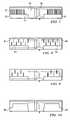
- FIG. 2depicts one embodiment of another view of antenna 10 .
- FIG. 2is a bottom view of the embodiment of the omnidirectional microstrip-coupled dipole antenna 10 of FIG. 1 .
- Features of the embodiment of the antenna 10include left teeth 20 , dipole gap 21 , right teeth 22 , feed point 23 , right antenna conductor 24 and left antenna conductor 25 .
- Right teeth 22are arranged beneath notch filter 12 (shown in FIG. 1 ).
- Feed point 23may be the outer coax conductor is soldered to ground (or where the outer coax is coupled using a SubMiniature version A (SMA) end launcher or other means). At least a portion of microstrip coupled line 11 is approximately above feed point 23 .
- SMASubMiniature version A
- the radiating element(s) of antenna 10may be driven by the microstrip coupled line 11 where the radiating element(s) are arranged underneath microstrip coupled line 11 .
- the length of the radiating elementmay substantially determine the frequency of antenna 10 , and the dimensions of the microstrip coupled line 11 determine the match within that frequency range.
- Microstrip coupled line 11may also bend over dipole gap 21 and serve to at least partially couple the energy from a coax conductor to the dipole gap.
- a signalmay be transferred from the center conductor of the coax conductor into microstrip coupled line 11 and where microstrip coupled line 11 is over the dipole gap 11 , energy is fed into the dipole gap 11 and dipole radiation behavior results (e.g. a dipole at the bottom of antenna 10 having an additional dipole pattern.
- Left teeth 20 and right teeth 22may serve at least two purposes. One purpose is extending the bandwidth of transmissions from antenna 10 . The second purpose is that the right teeth 23 together with the notch filter 12 may implement a sharp (in terms of insertion loss) notch. It will be apparent that the orientation, geometry, number and spacing of teeth 20 , 22 may vary, or teeth 20 , 22 may be eliminated altogether, according to the embodiment desired.
- left teeth 20 and right teeth 22may be substantially aligned along the same axis and have a certain amount of space between them (i.e. in a comb pattern). Having teeth 20 , 22 along an edge, or proximate to an edge, of antenna 10 , such as in FIG. 2 , may allow metal to remain across the bottom of antenna 10 , increasing performance.
- FIG. 3depicts a composite view of an embodiment of the omnidirectional microstrip-coupled dipole antenna.
- This composite viewincludes features shown in the top and bottom views of FIG. 1 and FIG. 2 .
- Features of the embodiment of the antennaeinclude microstrip coupled line 11 , notch filter 12 , notched matching stub 15 , matching stub 13 , top feed point 14 , dipole gap 21 , bottom feed point 23 , left teeth 20 , right teeth 22 , right antenna conductor 24 , and left antenna conductor 25 . Notice the placement of notch filter 12 with respect to right teeth 22 . As shown in the embodiment of FIG. 3 , notch filter 12 may overlap right teeth 22 .
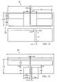
- Particular dimensions for one embodiment of an antennasuch as is depicted in FIGS. 1-3 operable in approximately the 3.17 GHz to 4.75 GHz range are shown in FIGS. 4 and 5 .
- FIG. 6a schematic view of another embodiment of an omnidirectional microstrip-coupled dipole antenna is presented.
- Embodiments such as the one depicted in FIG. 6may be suited for manufacture using material with a lower dielectric constant and use in a frequency range between approximately 3.17 GHz and 4.75 GHz.
- the embodiment of FIG. 6may be manufactured using FR4, which has a dielectric constant in the range of about 4.2-4.6.
- omnidirectional microstrip-coupled dipole antenna 40may be larger than embodiments of the omnidirectional microstrip-coupled dipole antenna manufactured using a material having a high dielectric constant (e.g., about 10).
- Antenna 40includes microstrip 41 having a U-shaped hook configuration, as shown.
- microstrip 41may, in eon embodiment, have a first portion substantially oriented along a first axis, a second portion substantially oriented along a second axis perpendicular to the first axis and a third portion substantially oriented along the first axis.
- other embodimentsmay have microstrips having a vertical section, a quarter-circle section, or a horizontal section, much like microstrip 11 of FIGS. 1-3 .
- Antenna 40may also incorporate notches and/or combs similar to those described with respect to FIGS. 1-3 .
- Embodiments of antenna 40may be significantly narrower than typical antennas which operate in similar frequency range(s) and/or which are manufactured from material having a similar dielectric constant. As shown in FIG. 6 , antenna 40 can have dimensions of 38 mm by 15.5 mm. However, in other embodiment, these dimensions may be approximately 32 mm by 10 mm.
- antenna 40may have a very good transition from the signal fed by an incoming unbalanced coax to the balanced dipole of the antenna 40 .
- the dimensions of the dipole conductorsmay be approximately 15.5 mm or, in some cases may as small as 10 mm or smaller.
- embodiments of the present inventionmay be applied to achieve almost any bandwidth desired.
- FIG. 7embodiments of an embodiment of the present invention is depicted with a broadbanding scheme to achieve an extended bandwidth.
- teeth 51may be configured in conductors 53 and 55 such that a downward comb pattern is formed.
- cut-out portions 52 and 54may be removed from antenna conductors 53 and 55 , respectively.
- Dipole conductors 61 and 62are shown in a meanderline configuration.
- Dipole conductors 61 and 62include cutout portions 63 .
- the length and/or thickness of each cutout portions 63(which may be varied to change parameters of the antenna, for example, distance between cutout portions 63 , depth of portions 63 , number of portions 63 , etc.).
- the meanderline configurationmay also have the added effect of reducing the size the antenna.
- the zigzag patternincreases the path length and therefore shifts frequency operation to lower frequencies.
- Another meanderline configurationis shown in FIG. 9 .
- FIG. 10is a composite view of an embodiment of the omnidirectional microstrip-coupled dipole antenna having yet another broadbanding scheme. As shown, cutout portions 82 and 83 may be used absent comb structures. The extent of the cutout portions is limited by the area needed for electron travel. An embodiment such as this, having a launching structure with the dipole in the center, was used for the initial empirical models.
- FIG. 11is a schematic view of another embodiment of an antenna according to one embodiment of the invention.
- This embodimentmay be well suited for manufacture using lower dielectric material such as FR4 and may be relatively small ins size (compared with typical antennas of similar functionality).
- FIG. 12is a schematic view of yet another embodiment of an antenna according to an embodiment of the present invention.
- These antennasmay be dipole antennas, wherein the antenna is integrated with the groundplane and a transceiver such that an entire radio may be included on a single card, such as a card designed for use with a CardBus card, PMCIA Card, daughtercard etc.
- these antennasmay be implemented utilizing a single layer of the PCB with which they are implemented, while in other embodiments these antennas may only utilize two layers of the PCB.
- these antennasmay be designed for use in conjunction with particular applications, such as for use with a card to be used on a CardBus or as a duaghtercard, these antennas may be designed for use with a particular enclosure for the card (where the antenna may protrude from this enclosure or be surrounded by the enclosure). More specifically, the antenna may be designed in conjunction with a particular enclosure such that when the antenna is included on a card utilized with that enclosure the antenna may radiate substantially in the desired frequency range, as certain enclosures may increase the dielectric constant around the antenna and thus increase the radiating frequency of the antenna. This enclosure containing the card may then be utilized with a device (e.g. laptop) where it is desired to utilize a device with a UWB radio. In addition, embodiments of these antennas may utilize tapered slots to focus their radiation pattern in the endfire direction.
- a devicee.g. laptop
- embodiments of these antennasmay utilize tapered slots to focus their radiation pattern in the endfire direction.
- these antennasmay be driven directly from the transceiver itself.
- these antennasmay have the dipole over a small groundplane, in fact, the dipoles of the antenna may be integrated with the groundplane.
- These types of arrangementsmay beneficially serve to localize current on or near the groundplane with which antennas of this type are utilized. More particularly, when in these antennas are in use surface current may be localized to the top edge of the groundplane. This localized current may allow other components of the radio, including active components, to be placed near the ground plane without adversely affecting the performance of these antennas.
Landscapes
- Variable-Direction Aerials And Aerial Arrays (AREA)
- Details Of Aerials (AREA)
Abstract
Description
Claims (15)
Priority Applications (2)
| Application Number | Priority Date | Filing Date | Title |
|---|---|---|---|
| US11/480,233US7271779B2 (en) | 2005-06-30 | 2006-06-30 | Method, system and apparatus for an antenna |
| US11/893,284US7589690B1 (en) | 2005-06-30 | 2007-08-15 | Method, system and apparatus for an antenna |
Applications Claiming Priority (2)
| Application Number | Priority Date | Filing Date | Title |
|---|---|---|---|
| US69564505P | 2005-06-30 | 2005-06-30 | |
| US11/480,233US7271779B2 (en) | 2005-06-30 | 2006-06-30 | Method, system and apparatus for an antenna |
Related Child Applications (1)
| Application Number | Title | Priority Date | Filing Date |
|---|---|---|---|
| US11/893,284ContinuationUS7589690B1 (en) | 2005-06-30 | 2007-08-15 | Method, system and apparatus for an antenna |
Publications (2)
| Publication Number | Publication Date |
|---|---|
| US20070035462A1 US20070035462A1 (en) | 2007-02-15 |
| US7271779B2true US7271779B2 (en) | 2007-09-18 |
Family
ID=37742067
Family Applications (2)
| Application Number | Title | Priority Date | Filing Date |
|---|---|---|---|
| US11/480,233Expired - Fee RelatedUS7271779B2 (en) | 2005-06-30 | 2006-06-30 | Method, system and apparatus for an antenna |
| US11/893,284Expired - Fee RelatedUS7589690B1 (en) | 2005-06-30 | 2007-08-15 | Method, system and apparatus for an antenna |
Family Applications After (1)
| Application Number | Title | Priority Date | Filing Date |
|---|---|---|---|
| US11/893,284Expired - Fee RelatedUS7589690B1 (en) | 2005-06-30 | 2007-08-15 | Method, system and apparatus for an antenna |
Country Status (1)
| Country | Link |
|---|---|
| US (2) | US7271779B2 (en) |
Cited By (64)
| Publication number | Priority date | Publication date | Assignee | Title |
|---|---|---|---|---|
| US20070143078A1 (en)* | 2001-03-26 | 2007-06-21 | Martin Vetterli | Sampling method, reconstruction method, and device for sampling and/or reconstructing signals |
| US20080117939A1 (en)* | 2006-11-16 | 2008-05-22 | Qualcomm Incorporated | Multiple access techniques for a wireless communiation medium |
| US20090002251A1 (en)* | 2007-06-06 | 2009-01-01 | Jean-Francois Pintos | Wideband antennas |
| US20090115673A1 (en)* | 2007-09-04 | 2009-05-07 | Sierra Wireless, Inc. | Antenna Configurations for Compact Device Wireless Communication |
| US20090115672A1 (en)* | 2007-09-04 | 2009-05-07 | Sierra Wireless, Inc. | Antenna Configurations for Compact Device Wireless Communication |
| US20090115670A1 (en)* | 2007-09-04 | 2009-05-07 | Sierra Wireless, Inc. | Antenna Configurations for Compact Device Wireless Communication |
| US20090124215A1 (en)* | 2007-09-04 | 2009-05-14 | Sierra Wireless, Inc. | Antenna Configurations for Compact Device Wireless Communication |
| US20090122847A1 (en)* | 2007-09-04 | 2009-05-14 | Sierra Wireless, Inc. | Antenna Configurations for Compact Device Wireless Communication |
| US7576605B2 (en) | 2006-04-20 | 2009-08-18 | Qualcomm Incorporated | Low power output stage |
| US7576672B2 (en) | 2007-07-18 | 2009-08-18 | Qualcomm Incorporated | Adaptive Dynamic Range Control |
| US7589690B1 (en)* | 2005-06-30 | 2009-09-15 | Alereon, Inc. | Method, system and apparatus for an antenna |
| US7592878B2 (en) | 2007-04-05 | 2009-09-22 | Qualcomm Incorporated | Method and apparatus for generating oscillating signals |
| US20100005371A1 (en)* | 2008-07-07 | 2010-01-07 | Qualcomm Incorporated | System and method of puncturing pulses in a receiver or transmitter |
| USD611039S1 (en)* | 2008-08-21 | 2010-03-02 | Panasonic Corporation | Antenna |
| USD611038S1 (en)* | 2008-08-21 | 2010-03-02 | Panasonic Corporation | Antenna |
| US7716001B2 (en) | 2006-11-15 | 2010-05-11 | Qualcomm Incorporated | Delay line calibration |
| US7812667B2 (en) | 2008-03-10 | 2010-10-12 | Qualcomm Incorporated | System and method of enabling a signal processing device in a relatively fast manner to process a low duty cycle signal |
| US7834482B2 (en) | 2007-04-23 | 2010-11-16 | Qualcomm Incorporated | Apparatus and method for generating fine timing from coarse timing source |
| US7855611B2 (en) | 2006-11-15 | 2010-12-21 | Qualcomm Incorporated | Delay line calibration |
| US7868689B2 (en) | 2008-04-08 | 2011-01-11 | Qualcomm Incorporated | Low power slicer-based demodulator for PPM |
| US7889753B2 (en) | 2006-11-16 | 2011-02-15 | Qualcomm Incorporated | Multiple access techniques for a wireless communication medium |
| US7952528B2 (en)* | 2007-09-04 | 2011-05-31 | Sierra Wireless, Inc. | Antenna configurations for compact device wireless communication |
| US7965805B2 (en) | 2007-09-21 | 2011-06-21 | Qualcomm Incorporated | Signal generator with signal tracking |
| US7974580B2 (en) | 2007-08-28 | 2011-07-05 | Qualcomm Incorporated | Apparatus and method for modulating an amplitude, phase or both of a periodic signal on a per cycle basis |
| US8005065B2 (en) | 2007-09-11 | 2011-08-23 | Qualcomm Incorporated | Keep-alive for wireless networks |
| US20110231657A1 (en)* | 2009-03-16 | 2011-09-22 | Qualcomm Incorporated | Apparatus and method for employing codes for telecommunications |
| US8059573B2 (en) | 2007-07-30 | 2011-11-15 | Qualcomm Incorporated | Method of pairing devices |
| US8103228B2 (en) | 2007-07-12 | 2012-01-24 | Qualcomm Incorporated | Method for determining line-of-sight (LOS) distance between remote communications devices |
| US8165080B2 (en) | 2008-08-22 | 2012-04-24 | Qualcomm Incorporated | Addressing schemes for wireless communication |
| US8233572B2 (en) | 2007-09-25 | 2012-07-31 | Qualcomm Incorporated | Interference mitigation for impulse-based communication |
| US8254595B2 (en) | 2008-03-25 | 2012-08-28 | Qualcomm Incorporated | System and method of companding an input signal of an energy detecting receiver |
| US8275343B2 (en) | 2008-03-10 | 2012-09-25 | Qualcomm Incorporated | System and method of using residual voltage from a prior operation to establish a bias voltage for a subsequent operation |
| US8275373B2 (en) | 2007-09-28 | 2012-09-25 | Qualcomm Incorporated | Randomization of periodic channel scans |
| US8289159B2 (en) | 2006-04-26 | 2012-10-16 | Qualcomm Incorporated | Wireless localization apparatus and method |
| US8326246B2 (en) | 2007-07-10 | 2012-12-04 | Qualcomm Incorporated | Super regenerative (SR) apparatus having plurality of parallel SR amplifiers tuned to distinct frequencies |
| US8363583B2 (en) | 2006-12-15 | 2013-01-29 | Qualcomm Incorporated | Channel access scheme for ultra-wide band communication |
| US8385474B2 (en) | 2007-09-21 | 2013-02-26 | Qualcomm Incorporated | Signal generator with adjustable frequency |
| US8406794B2 (en) | 2006-04-26 | 2013-03-26 | Qualcomm Incorporated | Methods and apparatuses of initiating communication in wireless networks |
| US8446976B2 (en) | 2007-09-21 | 2013-05-21 | Qualcomm Incorporated | Signal generator with adjustable phase |
| US8451710B2 (en) | 2006-04-26 | 2013-05-28 | Qualcomm Incorporated | Sub-packet pulse-based communications |
| US8473013B2 (en) | 2008-04-23 | 2013-06-25 | Qualcomm Incorporated | Multi-level duty cycling |
| US8483639B2 (en) | 2008-05-06 | 2013-07-09 | Qualcomm Incorporated | AGC for slicer-based low power demodulator |
| US8514911B2 (en) | 2009-05-13 | 2013-08-20 | Qualcomm Incorporated | Method and apparatus for clock drift compensation during acquisition in a wireless communication system |
| US8538345B2 (en) | 2007-10-09 | 2013-09-17 | Qualcomm Incorporated | Apparatus including housing incorporating a radiating element of an antenna |
| US8553744B2 (en) | 2009-01-06 | 2013-10-08 | Qualcomm Incorporated | Pulse arbitration for network communications |
| US8552903B2 (en) | 2006-04-18 | 2013-10-08 | Qualcomm Incorporated | Verified distance ranging |
| US8589720B2 (en) | 2008-04-15 | 2013-11-19 | Qualcomm Incorporated | Synchronizing timing mismatch by data insertion |
| US8600373B2 (en) | 2006-04-26 | 2013-12-03 | Qualcomm Incorporated | Dynamic distribution of device functionality and resource management |
| US8612693B2 (en) | 2009-03-19 | 2013-12-17 | Qualcomm Incorporated | Optimized transfer of packets in a resource constrained operating environment |
| US8644396B2 (en) | 2006-04-18 | 2014-02-04 | Qualcomm Incorporated | Waveform encoding for wireless applications |
| US8787440B2 (en) | 2008-07-25 | 2014-07-22 | Qualcomm Incorporated | Determination of receive data values |
| US8811456B2 (en) | 2006-04-19 | 2014-08-19 | Qualcomm Incorporated | Apparatus and method of low latency multi-hop communication |
| US8837724B2 (en) | 2007-03-27 | 2014-09-16 | Qualcomm Incorporated | Synchronization test for device authentication |
| US8886125B2 (en) | 2006-04-14 | 2014-11-11 | Qualcomm Incorporated | Distance-based association |
| US9083448B2 (en) | 2007-10-26 | 2015-07-14 | Qualcomm Incorporated | Preamble capture and medium access control |
| US9124357B2 (en) | 2006-04-20 | 2015-09-01 | Qualcomm Incorporated | Media access control for ultra-wide band communication |
| US9141961B2 (en) | 2007-06-20 | 2015-09-22 | Qualcomm Incorporated | Management of dynamic mobile coupons |
| US9215581B2 (en) | 2006-04-14 | 2015-12-15 | Qualcomm Incorported | Distance-based presence management |
| US9483769B2 (en) | 2007-06-20 | 2016-11-01 | Qualcomm Incorporated | Dynamic electronic coupon for a mobile environment |
| US9524502B2 (en) | 2007-06-20 | 2016-12-20 | Qualcomm Incorporated | Management of dynamic electronic coupons |
| US9590293B2 (en) | 2014-09-16 | 2017-03-07 | Google Inc. | GPS/WiFi battery antenna |
| US10542372B2 (en) | 2011-03-15 | 2020-01-21 | Qualcomm Incorporated | User identification within a physical merchant location through the use of a wireless network |
| EP3654448A1 (en) | 2017-11-28 | 2020-05-20 | Taoglas Group Holdings Limited | In-glass high performance antenna |
| US11108141B2 (en) | 2018-09-12 | 2021-08-31 | Taoglas Group Holdings Limited | Embedded patch antennas, systems and methods |
Families Citing this family (7)
| Publication number | Priority date | Publication date | Assignee | Title |
|---|---|---|---|---|
| US7414583B2 (en)* | 2004-12-08 | 2008-08-19 | Electronics And Telecommunications Research Institute | PIFA, RFID tag using the same and antenna impedance adjusting method thereof |
| US7728781B2 (en)* | 2008-03-06 | 2010-06-01 | Tc License Ltd. | Transmission line notch filter |
| AU325814S (en)* | 2008-12-26 | 2009-04-23 | Nec Corp | Antenna |
| FR3043867B1 (en)* | 2015-11-13 | 2018-09-21 | Lynred | ANALOGUE-DIGITAL CONVERTER WITH SUCCESSIVE APPROXIMATIONS. |
| CN105529527A (en)* | 2016-01-25 | 2016-04-27 | 南京邮电大学 | A Microstrip Antenna |
| US20180007627A1 (en)* | 2016-06-29 | 2018-01-04 | Intel Corporation | Modified uf-ofdm for enhanced wi-fi iot ul transmission |
| US11181613B2 (en)* | 2018-12-11 | 2021-11-23 | Waymo Llc | Filtering undesired polarization of signals transmitted from a chip to a waveguide unit |
Citations (8)
| Publication number | Priority date | Publication date | Assignee | Title |
|---|---|---|---|---|
| US3813674A (en)* | 1972-01-05 | 1974-05-28 | Secr Defence | Cavity backed dipole-slot antenna for circular polarization |
| US3845490A (en)* | 1973-05-03 | 1974-10-29 | Gen Electric | Stripline slotted balun dipole antenna |
| US4005430A (en)* | 1975-01-17 | 1977-01-25 | Etat Francais Represente Par Le Delegue Ministeriel Pour L'armement | Thick folded dipole which is tuneable within a frequency band of two octaves |
| US4825220A (en)* | 1986-11-26 | 1989-04-25 | General Electric Company | Microstrip fed printed dipole with an integral balun |
| US20050035919A1 (en)* | 2003-08-15 | 2005-02-17 | Fan Yang | Multi-band printed dipole antenna |
| US6961028B2 (en)* | 2003-01-17 | 2005-11-01 | Lockheed Martin Corporation | Low profile dual frequency dipole antenna structure |
| US20060170607A1 (en)* | 2005-02-01 | 2006-08-03 | Fujitsu Limited | Meander line antenna |
| US20060238433A1 (en)* | 2005-03-01 | 2006-10-26 | Joymax Electronics Co., Ltd. | Antenna assembly having different signal emitting direction |
Family Cites Families (3)
| Publication number | Priority date | Publication date | Assignee | Title |
|---|---|---|---|---|
| JP3085524B2 (en)* | 1996-11-18 | 2000-09-11 | 日本電業工作株式会社 | Dipole antenna with reflector |
| KR100846486B1 (en)* | 2002-05-06 | 2008-07-17 | 삼성전자주식회사 | Image removal antenna |
| US7271779B2 (en)* | 2005-06-30 | 2007-09-18 | Alereon, Inc. | Method, system and apparatus for an antenna |
- 2006
- 2006-06-30USUS11/480,233patent/US7271779B2/ennot_activeExpired - Fee Related
- 2007
- 2007-08-15USUS11/893,284patent/US7589690B1/ennot_activeExpired - Fee Related
Patent Citations (8)
| Publication number | Priority date | Publication date | Assignee | Title |
|---|---|---|---|---|
| US3813674A (en)* | 1972-01-05 | 1974-05-28 | Secr Defence | Cavity backed dipole-slot antenna for circular polarization |
| US3845490A (en)* | 1973-05-03 | 1974-10-29 | Gen Electric | Stripline slotted balun dipole antenna |
| US4005430A (en)* | 1975-01-17 | 1977-01-25 | Etat Francais Represente Par Le Delegue Ministeriel Pour L'armement | Thick folded dipole which is tuneable within a frequency band of two octaves |
| US4825220A (en)* | 1986-11-26 | 1989-04-25 | General Electric Company | Microstrip fed printed dipole with an integral balun |
| US6961028B2 (en)* | 2003-01-17 | 2005-11-01 | Lockheed Martin Corporation | Low profile dual frequency dipole antenna structure |
| US20050035919A1 (en)* | 2003-08-15 | 2005-02-17 | Fan Yang | Multi-band printed dipole antenna |
| US20060170607A1 (en)* | 2005-02-01 | 2006-08-03 | Fujitsu Limited | Meander line antenna |
| US20060238433A1 (en)* | 2005-03-01 | 2006-10-26 | Joymax Electronics Co., Ltd. | Antenna assembly having different signal emitting direction |
Cited By (88)
| Publication number | Priority date | Publication date | Assignee | Title |
|---|---|---|---|---|
| US8077757B2 (en) | 2001-03-26 | 2011-12-13 | Qualcomm Incorporated | Sampling method for a spread spectrum communication system |
| US8031820B2 (en) | 2001-03-26 | 2011-10-04 | Qualcomm Incorporated | Sampling method, reconstruction method, and device for sampling and/or reconstructing signals |
| US20070143078A1 (en)* | 2001-03-26 | 2007-06-21 | Martin Vetterli | Sampling method, reconstruction method, and device for sampling and/or reconstructing signals |
| US8160194B2 (en) | 2001-03-26 | 2012-04-17 | Qualcomm Incorporated | Sampling method, reconstruction method, and device for sampling and/or reconstructing signals |
| US7991095B2 (en) | 2001-03-26 | 2011-08-02 | Qualcomm Incorporated | Sampling method, reconstruction method, and device for sampling and/or reconstructing signals |
| US7589690B1 (en)* | 2005-06-30 | 2009-09-15 | Alereon, Inc. | Method, system and apparatus for an antenna |
| US9510383B2 (en) | 2006-04-14 | 2016-11-29 | Qualcomm Incorporated | System and method of associating devices based on actuation of input devices and signal strength |
| US8886125B2 (en) | 2006-04-14 | 2014-11-11 | Qualcomm Incorporated | Distance-based association |
| US9215581B2 (en) | 2006-04-14 | 2015-12-15 | Qualcomm Incorported | Distance-based presence management |
| US9591470B2 (en) | 2006-04-14 | 2017-03-07 | Qualcomm Incorporated | System and method for enabling operations based on distance to and motion of remote device |
| US8552903B2 (en) | 2006-04-18 | 2013-10-08 | Qualcomm Incorporated | Verified distance ranging |
| US8654868B2 (en) | 2006-04-18 | 2014-02-18 | Qualcomm Incorporated | Offloaded processing for wireless applications |
| US8644396B2 (en) | 2006-04-18 | 2014-02-04 | Qualcomm Incorporated | Waveform encoding for wireless applications |
| US8811456B2 (en) | 2006-04-19 | 2014-08-19 | Qualcomm Incorporated | Apparatus and method of low latency multi-hop communication |
| US7576605B2 (en) | 2006-04-20 | 2009-08-18 | Qualcomm Incorporated | Low power output stage |
| US9124357B2 (en) | 2006-04-20 | 2015-09-01 | Qualcomm Incorporated | Media access control for ultra-wide band communication |
| US8289159B2 (en) | 2006-04-26 | 2012-10-16 | Qualcomm Incorporated | Wireless localization apparatus and method |
| US8527016B2 (en) | 2006-04-26 | 2013-09-03 | Qualcomm Incorporated | Wireless device communication with multiple peripherals |
| US8451710B2 (en) | 2006-04-26 | 2013-05-28 | Qualcomm Incorporated | Sub-packet pulse-based communications |
| US8406794B2 (en) | 2006-04-26 | 2013-03-26 | Qualcomm Incorporated | Methods and apparatuses of initiating communication in wireless networks |
| US8600373B2 (en) | 2006-04-26 | 2013-12-03 | Qualcomm Incorporated | Dynamic distribution of device functionality and resource management |
| US8553745B2 (en) | 2006-04-26 | 2013-10-08 | Qualcomm Incorporated | Inter-pulse duty cycling |
| US7855611B2 (en) | 2006-11-15 | 2010-12-21 | Qualcomm Incorporated | Delay line calibration |
| US8698572B2 (en) | 2006-11-15 | 2014-04-15 | Qualcomm Incorporated | Delay line calibration |
| US7716001B2 (en) | 2006-11-15 | 2010-05-11 | Qualcomm Incorporated | Delay line calibration |
| US7889753B2 (en) | 2006-11-16 | 2011-02-15 | Qualcomm Incorporated | Multiple access techniques for a wireless communication medium |
| US8014425B2 (en) | 2006-11-16 | 2011-09-06 | Qualcomm Incorporated | Multiple access techniques for a wireless communiation medium |
| US20080117939A1 (en)* | 2006-11-16 | 2008-05-22 | Qualcomm Incorporated | Multiple access techniques for a wireless communiation medium |
| US8363583B2 (en) | 2006-12-15 | 2013-01-29 | Qualcomm Incorporated | Channel access scheme for ultra-wide band communication |
| US8837724B2 (en) | 2007-03-27 | 2014-09-16 | Qualcomm Incorporated | Synchronization test for device authentication |
| US7902936B2 (en) | 2007-04-05 | 2011-03-08 | Qualcomm Incorporated | Method and apparatus for generating oscillating signals |
| US7592878B2 (en) | 2007-04-05 | 2009-09-22 | Qualcomm Incorporated | Method and apparatus for generating oscillating signals |
| US7834482B2 (en) | 2007-04-23 | 2010-11-16 | Qualcomm Incorporated | Apparatus and method for generating fine timing from coarse timing source |
| US20090002251A1 (en)* | 2007-06-06 | 2009-01-01 | Jean-Francois Pintos | Wideband antennas |
| US8284113B2 (en)* | 2007-06-06 | 2012-10-09 | Thomson Licensing | Wideband antennas |
| US9141961B2 (en) | 2007-06-20 | 2015-09-22 | Qualcomm Incorporated | Management of dynamic mobile coupons |
| US9483769B2 (en) | 2007-06-20 | 2016-11-01 | Qualcomm Incorporated | Dynamic electronic coupon for a mobile environment |
| US9524502B2 (en) | 2007-06-20 | 2016-12-20 | Qualcomm Incorporated | Management of dynamic electronic coupons |
| US9747613B2 (en) | 2007-06-20 | 2017-08-29 | Qualcomm Incorporated | Dynamic electronic coupon for a mobile environment |
| US8326246B2 (en) | 2007-07-10 | 2012-12-04 | Qualcomm Incorporated | Super regenerative (SR) apparatus having plurality of parallel SR amplifiers tuned to distinct frequencies |
| US8103228B2 (en) | 2007-07-12 | 2012-01-24 | Qualcomm Incorporated | Method for determining line-of-sight (LOS) distance between remote communications devices |
| US7576672B2 (en) | 2007-07-18 | 2009-08-18 | Qualcomm Incorporated | Adaptive Dynamic Range Control |
| US8059573B2 (en) | 2007-07-30 | 2011-11-15 | Qualcomm Incorporated | Method of pairing devices |
| US8406693B2 (en) | 2007-08-28 | 2013-03-26 | Qualcomm Incorporated | Apparatus and method for modulating an amplitude, phase or both of a periodic signal on a per cycle basis |
| US7974580B2 (en) | 2007-08-28 | 2011-07-05 | Qualcomm Incorporated | Apparatus and method for modulating an amplitude, phase or both of a periodic signal on a per cycle basis |
| US20090115670A1 (en)* | 2007-09-04 | 2009-05-07 | Sierra Wireless, Inc. | Antenna Configurations for Compact Device Wireless Communication |
| US8049671B2 (en) | 2007-09-04 | 2011-11-01 | Sierra Wireless, Inc. | Antenna configurations for compact device wireless communication |
| US20090124215A1 (en)* | 2007-09-04 | 2009-05-14 | Sierra Wireless, Inc. | Antenna Configurations for Compact Device Wireless Communication |
| US7916090B2 (en) | 2007-09-04 | 2011-03-29 | Sierra Wireless, Inc. | Antenna configurations for compact device wireless communication |
| US7952528B2 (en)* | 2007-09-04 | 2011-05-31 | Sierra Wireless, Inc. | Antenna configurations for compact device wireless communication |
| US20090115672A1 (en)* | 2007-09-04 | 2009-05-07 | Sierra Wireless, Inc. | Antenna Configurations for Compact Device Wireless Communication |
| US20090115673A1 (en)* | 2007-09-04 | 2009-05-07 | Sierra Wireless, Inc. | Antenna Configurations for Compact Device Wireless Communication |
| US20090122847A1 (en)* | 2007-09-04 | 2009-05-14 | Sierra Wireless, Inc. | Antenna Configurations for Compact Device Wireless Communication |
| US8059046B2 (en) | 2007-09-04 | 2011-11-15 | Sierra Wireless, Inc. | Antenna configurations for compact device wireless communication |
| US8005065B2 (en) | 2007-09-11 | 2011-08-23 | Qualcomm Incorporated | Keep-alive for wireless networks |
| US7965805B2 (en) | 2007-09-21 | 2011-06-21 | Qualcomm Incorporated | Signal generator with signal tracking |
| US8446976B2 (en) | 2007-09-21 | 2013-05-21 | Qualcomm Incorporated | Signal generator with adjustable phase |
| US8385474B2 (en) | 2007-09-21 | 2013-02-26 | Qualcomm Incorporated | Signal generator with adjustable frequency |
| US8233572B2 (en) | 2007-09-25 | 2012-07-31 | Qualcomm Incorporated | Interference mitigation for impulse-based communication |
| US8275373B2 (en) | 2007-09-28 | 2012-09-25 | Qualcomm Incorporated | Randomization of periodic channel scans |
| US8538345B2 (en) | 2007-10-09 | 2013-09-17 | Qualcomm Incorporated | Apparatus including housing incorporating a radiating element of an antenna |
| US9083448B2 (en) | 2007-10-26 | 2015-07-14 | Qualcomm Incorporated | Preamble capture and medium access control |
| US7812667B2 (en) | 2008-03-10 | 2010-10-12 | Qualcomm Incorporated | System and method of enabling a signal processing device in a relatively fast manner to process a low duty cycle signal |
| US8275343B2 (en) | 2008-03-10 | 2012-09-25 | Qualcomm Incorporated | System and method of using residual voltage from a prior operation to establish a bias voltage for a subsequent operation |
| US8254595B2 (en) | 2008-03-25 | 2012-08-28 | Qualcomm Incorporated | System and method of companding an input signal of an energy detecting receiver |
| US7868689B2 (en) | 2008-04-08 | 2011-01-11 | Qualcomm Incorporated | Low power slicer-based demodulator for PPM |
| US8589720B2 (en) | 2008-04-15 | 2013-11-19 | Qualcomm Incorporated | Synchronizing timing mismatch by data insertion |
| US8473013B2 (en) | 2008-04-23 | 2013-06-25 | Qualcomm Incorporated | Multi-level duty cycling |
| US8483639B2 (en) | 2008-05-06 | 2013-07-09 | Qualcomm Incorporated | AGC for slicer-based low power demodulator |
| US20100005371A1 (en)* | 2008-07-07 | 2010-01-07 | Qualcomm Incorporated | System and method of puncturing pulses in a receiver or transmitter |
| US8375261B2 (en) | 2008-07-07 | 2013-02-12 | Qualcomm Incorporated | System and method of puncturing pulses in a receiver or transmitter |
| US8787440B2 (en) | 2008-07-25 | 2014-07-22 | Qualcomm Incorporated | Determination of receive data values |
| USD611038S1 (en)* | 2008-08-21 | 2010-03-02 | Panasonic Corporation | Antenna |
| USD611039S1 (en)* | 2008-08-21 | 2010-03-02 | Panasonic Corporation | Antenna |
| US8165080B2 (en) | 2008-08-22 | 2012-04-24 | Qualcomm Incorporated | Addressing schemes for wireless communication |
| US8848636B2 (en) | 2008-08-22 | 2014-09-30 | Qualcomm Incorporated | Addressing schemes for wireless communication |
| US8553744B2 (en) | 2009-01-06 | 2013-10-08 | Qualcomm Incorporated | Pulse arbitration for network communications |
| US20110231657A1 (en)* | 2009-03-16 | 2011-09-22 | Qualcomm Incorporated | Apparatus and method for employing codes for telecommunications |
| US8612693B2 (en) | 2009-03-19 | 2013-12-17 | Qualcomm Incorporated | Optimized transfer of packets in a resource constrained operating environment |
| US8514911B2 (en) | 2009-05-13 | 2013-08-20 | Qualcomm Incorporated | Method and apparatus for clock drift compensation during acquisition in a wireless communication system |
| US10542372B2 (en) | 2011-03-15 | 2020-01-21 | Qualcomm Incorporated | User identification within a physical merchant location through the use of a wireless network |
| US9590293B2 (en) | 2014-09-16 | 2017-03-07 | Google Inc. | GPS/WiFi battery antenna |
| EP3654448A1 (en) | 2017-11-28 | 2020-05-20 | Taoglas Group Holdings Limited | In-glass high performance antenna |
| US10910692B2 (en) | 2017-11-28 | 2021-02-02 | Taoglas Group Holdings Limited | In-glass high performance antenna |
| US11509036B2 (en) | 2017-11-28 | 2022-11-22 | Taoglas Group Holdings Limited | In-glass high performance antenna |
| US12015189B2 (en) | 2017-11-28 | 2024-06-18 | Taoglas Group Holdings Limited | In-glass high performance antenna |
| US12394880B2 (en) | 2017-11-28 | 2025-08-19 | Taoglas Group Holdings Limited | Methods for fabricating an antenna and a shielded transmission line |
| US11108141B2 (en) | 2018-09-12 | 2021-08-31 | Taoglas Group Holdings Limited | Embedded patch antennas, systems and methods |
Also Published As
| Publication number | Publication date |
|---|---|
| US20070035462A1 (en) | 2007-02-15 |
| US7589690B1 (en) | 2009-09-15 |
Similar Documents
| Publication | Publication Date | Title |
|---|---|---|
| US7271779B2 (en) | Method, system and apparatus for an antenna | |
| US7450072B2 (en) | Modified inverted-F antenna for wireless communication | |
| US8081122B2 (en) | Folded slotted monopole antenna | |
| US9502770B2 (en) | Compact multiple-band antenna for wireless devices | |
| TW552742B (en) | An integrated antenna for laptop applications | |
| EP2047563B1 (en) | Embedded multi-mode antenna architectures for wireless devices | |
| EP1684382A1 (en) | Small ultra wideband antenna having unidirectional radiation pattern | |
| EP2683030B1 (en) | Wideband monopole antenna and electronic device | |
| US20110309985A1 (en) | Wideband printed circuit board-printed antenna for radio frequency front end circuit | |
| CN103378420B (en) | Antenna system | |
| US20110156971A1 (en) | Wide band antenna | |
| US8416137B2 (en) | Low-profile wide-bandwidth radio frequency antenna | |
| CN103943942A (en) | Antenna and portable device with said antenna | |
| JP2007135212A (en) | Multiband antenna apparatus | |
| US10629992B2 (en) | Antenna system for matching an impedance | |
| EP2736119A1 (en) | Printed wide band monopole antenna module | |
| US20080278390A1 (en) | Ultra Wide Band Notch Antenna Assembly for Rf Communication Equipment | |
| EP4542771A1 (en) | Antenna structure and electronic device | |
| CN218569218U (en) | Slot antenna and communication equipment | |
| Zhao et al. | Compact printed patch and bent-patch monopole Ultra-Wideband (UWB) antennas for mobile terminals | |
| JP4935256B2 (en) | Antenna device | |
| Magray et al. | Co-design of 4G LTE and Millimeter-Wave 5G Antennas for Future Mobile Devices | |
| CN101740858A (en) | Antenna for receiving radio wave, electronic device incorporating the same, and method for manufacturing the antenna | |
| US7768464B2 (en) | Antenna device | |
| JP2010068122A (en) | Wideband antenna |
Legal Events
| Date | Code | Title | Description |
|---|---|---|---|
| AS | Assignment | Owner name:ALEREON, INC., TEXAS Free format text:ASSIGNMENT OF ASSIGNORS INTEREST;ASSIGNOR:HERTEL, THORSTEN W.;REEL/FRAME:018488/0032 Effective date:20061024 | |
| AS | Assignment | Owner name:VENTURE LENDING & LEASING IV, INC., AND VENTURE LE Free format text:SECURITY AGREEMENT;ASSIGNOR:ALEREON, INC.;REEL/FRAME:020637/0540 Effective date:20080213 | |
| FPAY | Fee payment | Year of fee payment:4 | |
| AS | Assignment | Owner name:ALEREON, INC., TEXAS Free format text:RELEASE BY SECURED PARTY;ASSIGNOR:VENTURE LENDING & LEASING IV, INC.;REEL/FRAME:027982/0814 Effective date:20120330 Owner name:ALEREON, INC., TEXAS Free format text:RELEASE BY SECURED PARTY;ASSIGNOR:VENTURE LENDING & LEASING V, INC.;REEL/FRAME:027982/0868 Effective date:20120330 | |
| AS | Assignment | Owner name:ENHANCED JOBS FOR TEXAS FUND, LLC, NEW YORK Free format text:SECURITY AGREEMENT;ASSIGNOR:ALEREON, INC.;REEL/FRAME:028039/0323 Effective date:20120412 Owner name:ENHANCED CAPITAL TEXAS FUND II, LLC, NEW YORK Free format text:SECURITY AGREEMENT;ASSIGNOR:ALEREON, INC.;REEL/FRAME:028039/0323 Effective date:20120412 | |
| AS | Assignment | Owner name:ENHANCED CREDIT SUPPORTED LOAN FUND, LP, NEW YORK Free format text:SECURITY AGREEMENT;ASSIGNOR:ALEREON, INC.;REEL/FRAME:031948/0386 Effective date:20131227 Owner name:ALEREON, INC., TEXAS Free format text:RELEASE BY SECURED PARTY;ASSIGNORS:ENHANCED CAPITAL TEXAS FUND II, LLC;ENHANCED JOBS FOR TEXAS FUND, LLC;REEL/FRAME:031948/0065 Effective date:20131227 | |
| REMI | Maintenance fee reminder mailed | ||
| LAPS | Lapse for failure to pay maintenance fees | ||
| STCH | Information on status: patent discontinuation | Free format text:PATENT EXPIRED DUE TO NONPAYMENT OF MAINTENANCE FEES UNDER 37 CFR 1.362 | |
| FP | Lapsed due to failure to pay maintenance fee | Effective date:20150918 |