US7271420B2 - Monolitholic LED chip to emit multiple colors - Google Patents
Monolitholic LED chip to emit multiple colorsDownload PDFInfo
- Publication number
- US7271420B2 US7271420B2US11/176,696US17669605AUS7271420B2US 7271420 B2US7271420 B2US 7271420B2US 17669605 AUS17669605 AUS 17669605AUS 7271420 B2US7271420 B2US 7271420B2
- Authority
- US
- United States
- Prior art keywords
- color emission
- contact layer
- electrical connection
- layer
- color
- Prior art date
- Legal status (The legal status is an assumption and is not a legal conclusion. Google has not performed a legal analysis and makes no representation as to the accuracy of the status listed.)
- Expired - Lifetime, expires
Links
Images


Classifications
- H—ELECTRICITY
- H10—SEMICONDUCTOR DEVICES; ELECTRIC SOLID-STATE DEVICES NOT OTHERWISE PROVIDED FOR
- H10H—INORGANIC LIGHT-EMITTING SEMICONDUCTOR DEVICES HAVING POTENTIAL BARRIERS
- H10H20/00—Individual inorganic light-emitting semiconductor devices having potential barriers, e.g. light-emitting diodes [LED]
- H10H20/80—Constructional details
- H10H20/83—Electrodes
- H10H20/831—Electrodes characterised by their shape
- H10H20/8312—Electrodes characterised by their shape extending at least partially through the bodies
- H—ELECTRICITY
- H10—SEMICONDUCTOR DEVICES; ELECTRIC SOLID-STATE DEVICES NOT OTHERWISE PROVIDED FOR
- H10H—INORGANIC LIGHT-EMITTING SEMICONDUCTOR DEVICES HAVING POTENTIAL BARRIERS
- H10H29/00—Integrated devices, or assemblies of multiple devices, comprising at least one light-emitting semiconductor element covered by group H10H20/00
- H10H29/10—Integrated devices comprising at least one light-emitting semiconductor component covered by group H10H20/00
- H—ELECTRICITY
- H10—SEMICONDUCTOR DEVICES; ELECTRIC SOLID-STATE DEVICES NOT OTHERWISE PROVIDED FOR
- H10H—INORGANIC LIGHT-EMITTING SEMICONDUCTOR DEVICES HAVING POTENTIAL BARRIERS
- H10H20/00—Individual inorganic light-emitting semiconductor devices having potential barriers, e.g. light-emitting diodes [LED]
- H10H20/80—Constructional details
- H10H20/81—Bodies
- H10H20/822—Materials of the light-emitting regions
- H10H20/824—Materials of the light-emitting regions comprising only Group III-V materials, e.g. GaP
- H10H20/825—Materials of the light-emitting regions comprising only Group III-V materials, e.g. GaP containing nitrogen, e.g. GaN
Definitions
- LEDsLight emitting diodes
- LEDsare expected to the source of light for the next generation lighting which will replace incandescent bulbs and fluourescent lights.
- White light and other color LEDswill be essential for different applications.
- LED chipsemit light centered around one wavelength, which would be considered monochromatic. Multiple colors including white are only generated by assembling several LEDs of different colors or by second step excitation. For example, white light an be generated by mixing red, green and blue, or using blue to excite yellow phosphor in order to generate white light.
- Chipsare disclosed that can produce red, green, and blue light all together or individually. By controlling the light intensity of light emitted, different colors of light including white can be achieved in a single chip.
- LED chipthat can emit multiple colors, such as red, green and blue, is provided below and in the appended figures.
- Other LED chips that selectively emit 2 or more colors of light of any desired color (wavelength)can be constructed using the principles disclosed below and in the figures.
- the chipmay be controlled so that only one color of light is emitted, so that all colors of light that the chip is capable of emitting are emitted, or so that a subset of the colors of light which the chip is capable of emitting are emitted. If all light emission regions of the chip are powered, white light can be emitted.
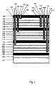
- a light emitting diode (“LED”) semiconductor chip structureis depicted that can emit multiple colors (different wavelengths) of light. Three are provided in the chip structure in order to three different colors of light, such as red, green, and blue color. Those three chips structures are built or grown on a single substrate 101 . Each structure to emit the light can be controlled individually.
- 101is a substrate, which can be an appropriate material, such as Si, GaAs, GaN, AlN, SiC, Sapphire or others.
- 102is a buffer layer to eliminate lattice mismatch defects between the substrate and epitaxial layers.
- the buffer layer 102 layercan be any appropriate material such as GaN.
- 103is a semi-insulating layer or dielectric layer, such as GaN.
- 105is a contact layer for providing electrical contact, which can be, for example, GaN, AlGaN, GalnN. This layer may be heavily doped with either N+ or P+ doped for establishing contacts. This layer can be coated with reflection layer 104 to reflect all light back in a useful direction.
- 106is the cladding layer for emission of light of one color (wavelength) such as red. This layer can be GaN, AlGaN, GalnN, GaNP or other materials.
- 107is the emitting or active layer for light of a desired color such as red, which can be GalnP, AlGalnP, GalnN, or GaNP.
- 108is the cladding layer for layer 107 , and can be GaN, AlGaN, GalnN, GaNP or other materials.
- 109is the contact layer for electrical contact, which can be GaiN, AlGaN, GalnN. This layer can be heavily doped with either N+ or P+ doped for establishing contacts.
- 110is a semi-insulating layer or dielectric layer, which can be GaN or others. It should be noted from the prior art that dielectric layer 110 may be comprised of a single layer or a plurality of sub-layers. For convenience this Specification will describe and depict the dielectric layers as if they were single, though the term is not intended to exclude the use of sub-layers.
- the electrical contact for this structureis through via contact hole 111 , which was etched through layers above.
- An insulation layer 112is laid inside the wall of contact hole 111 and a conductive metal filling 113 is used to make an electrical contact from the top.
- Similar structures 114 (electrical contact structure), 115 (insulation layer) and 116 (conductive metal filling)are used to make another electrical contact.
- the LED deviceto emit a first color such as red separately controlled from operation of the rest of the LED chip.
- 117is the contact layer for electrical contact, which can be GaN, AlGaN, GalnN. This layer is heavily either N+ or P+ doped for establishing contact.
- 118is the cladding layer for emission of light of another color, in this example green light. This layer can be GaN, AlGaN, GalnN, GaNP.
- 119is the emitting or active layer for green color light, which can be GalnP, AlGalnP, GalnN, or GaNP.
- 120is the cladding layer for green light emission, and this layer can be GaN, AlGaN, GalnN, GaNP.
- 121is the contact layer for electrical contact for green light emission, which can be GaN, AlGaN, GalnN. This layer is heavily either N+ or P+ doped for establishing electrical contact.
- 121is a semi-insulating layer or dielectric layer, which can be GaN or other materials.
- the electrical contact for this structureis through via generally vertical or top-down structure 123 , which was etched through layers above 121 .
- An insulation layer 124is laid inside wall of contact hole 123 and a metal filling 125 is used to make an electrical contact from the top.
- 126is another contact hole
- 127is another insulation layer
- 128is metal filling for another deep electrical contact. Using these structures, the LED device can emit different colors selectively.
- 129is the contact layer for electrical contact, which can be GaN, AlGaN, GalnN. This layer is heavily either N+ or P+ doped for use as a contact.
- 130is the cladding layer for blue color emission, this layer can be GaN, AlGaN, GalnN, GaNP.
- 131is the emitting or active layer for emitting blue light, which can be GalnN, or AlGaN.
- 132is the cladding layer for blue color emission, this layer can be GaN, AlGaN, GalnN.
- 133is the contact layer for electrical contact, which can be GaN, AlGaN, GalnN. This layer is heavily either N+ or P+ doped for use as a contacte.
- 134is a semi-insulating layer or dielectric layer, which can be GaN or other thin file like Si 3 N 4 and SiO 2 .
- the electrical contact for this structureis through via structure 135 , which was etched through layers above 133 .
- An insulation layer 136is laid inside wall of contact hole 133 and a metal filling 137 is used to make an electrical contact from the top.
- Similar deep contact structure 138has a hold in which an insulation layer 139 and a conductive metal filling 140 are present to power the blue color layer of the LED chip.
- FIG. 2depicts top view of an LED chip 201 than can emit multiple colors.
- 202is the dielectric pad for electrode 113
- 203is the dielectric pad for electrode 116 .
- 113 and 116control red color emission.
- 205is the dielectric pad for electrode 124
- 206is the dielectric pad for electrode 128 .
- 124 and 128control the green color emission.
- 206is the dielectric pad for electrode 137 and 208 is the dielectric pad for electrode 140 . 137 and 140 control the blue color emission.
Landscapes
- Led Devices (AREA)
- Led Device Packages (AREA)
Abstract
Description
Claims (16)
Priority Applications (2)
| Application Number | Priority Date | Filing Date | Title |
|---|---|---|---|
| US11/176,696US7271420B2 (en) | 2004-07-07 | 2005-07-07 | Monolitholic LED chip to emit multiple colors |
| US11/689,233US20070170444A1 (en) | 2004-07-07 | 2007-03-21 | Integrated LED Chip to Emit Multiple Colors and Method of Manufacturing the Same |
Applications Claiming Priority (2)
| Application Number | Priority Date | Filing Date | Title |
|---|---|---|---|
| US58598804P | 2004-07-07 | 2004-07-07 | |
| US11/176,696US7271420B2 (en) | 2004-07-07 | 2005-07-07 | Monolitholic LED chip to emit multiple colors |
Related Child Applications (1)
| Application Number | Title | Priority Date | Filing Date |
|---|---|---|---|
| US11/689,233Continuation-In-PartUS20070170444A1 (en) | 2004-07-07 | 2007-03-21 | Integrated LED Chip to Emit Multiple Colors and Method of Manufacturing the Same |
Publications (2)
| Publication Number | Publication Date |
|---|---|
| US20060027820A1 US20060027820A1 (en) | 2006-02-09 |
| US7271420B2true US7271420B2 (en) | 2007-09-18 |
Family
ID=35756564
Family Applications (1)
| Application Number | Title | Priority Date | Filing Date |
|---|---|---|---|
| US11/176,696Expired - LifetimeUS7271420B2 (en) | 2004-07-07 | 2005-07-07 | Monolitholic LED chip to emit multiple colors |
Country Status (1)
| Country | Link |
|---|---|
| US (1) | US7271420B2 (en) |
Cited By (234)
| Publication number | Priority date | Publication date | Assignee | Title |
|---|---|---|---|---|
| US20070131950A1 (en)* | 2005-12-13 | 2007-06-14 | Canon Kabushiki Kaisha | Light emitting element array and image forming apparatus |
| US20080136317A1 (en)* | 2006-12-06 | 2008-06-12 | General Electric Company | Illumination source providing enhanced color mixing |
| US20100084668A1 (en)* | 2008-10-03 | 2010-04-08 | Choi Hoi Wai | Semiconductor color-tunable broadband light sources and full-color microdisplays |
| US8113830B2 (en) | 2005-05-27 | 2012-02-14 | Kerr Corporation | Curing light instrument |
| US20120091474A1 (en)* | 2010-10-13 | 2012-04-19 | NuPGA Corporation | Novel semiconductor and optoelectronic devices |
| US8163581B1 (en) | 2010-10-13 | 2012-04-24 | Monolith IC 3D | Semiconductor and optoelectronic devices |
| US8203148B2 (en) | 2010-10-11 | 2012-06-19 | Monolithic 3D Inc. | Semiconductor device and structure |
| US8231383B2 (en) | 2002-08-08 | 2012-07-31 | Kerr Corporation | Curing light instrument |
| US8237228B2 (en) | 2009-10-12 | 2012-08-07 | Monolithic 3D Inc. | System comprising a semiconductor device and structure |
| US8273610B2 (en) | 2010-11-18 | 2012-09-25 | Monolithic 3D Inc. | Method of constructing a semiconductor device and structure |
| US8294159B2 (en) | 2009-10-12 | 2012-10-23 | Monolithic 3D Inc. | Method for fabrication of a semiconductor device and structure |
| US8362482B2 (en) | 2009-04-14 | 2013-01-29 | Monolithic 3D Inc. | Semiconductor device and structure |
| US8362800B2 (en) | 2010-10-13 | 2013-01-29 | Monolithic 3D Inc. | 3D semiconductor device including field repairable logics |
| US8373439B2 (en) | 2009-04-14 | 2013-02-12 | Monolithic 3D Inc. | 3D semiconductor device |
| US8373230B1 (en) | 2010-10-13 | 2013-02-12 | Monolithic 3D Inc. | Method for fabrication of a semiconductor device and structure |
| US8378715B2 (en) | 2009-04-14 | 2013-02-19 | Monolithic 3D Inc. | Method to construct systems |
| US8378494B2 (en) | 2009-04-14 | 2013-02-19 | Monolithic 3D Inc. | Method for fabrication of a semiconductor device and structure |
| US8379458B1 (en) | 2010-10-13 | 2013-02-19 | Monolithic 3D Inc. | Semiconductor device and structure |
| US8384426B2 (en) | 2009-04-14 | 2013-02-26 | Monolithic 3D Inc. | Semiconductor device and structure |
| US8405420B2 (en) | 2009-04-14 | 2013-03-26 | Monolithic 3D Inc. | System comprising a semiconductor device and structure |
| US8427200B2 (en) | 2009-04-14 | 2013-04-23 | Monolithic 3D Inc. | 3D semiconductor device |
| US8440542B2 (en) | 2010-10-11 | 2013-05-14 | Monolithic 3D Inc. | Semiconductor device and structure |
| US8450804B2 (en) | 2011-03-06 | 2013-05-28 | Monolithic 3D Inc. | Semiconductor device and structure for heat removal |
| US8461035B1 (en) | 2010-09-30 | 2013-06-11 | Monolithic 3D Inc. | Method for fabrication of a semiconductor device and structure |
| US8476145B2 (en) | 2010-10-13 | 2013-07-02 | Monolithic 3D Inc. | Method of fabricating a semiconductor device and structure |
| US8492886B2 (en) | 2010-02-16 | 2013-07-23 | Monolithic 3D Inc | 3D integrated circuit with logic |
| US8536023B2 (en) | 2010-11-22 | 2013-09-17 | Monolithic 3D Inc. | Method of manufacturing a semiconductor device and structure |
| US8541819B1 (en) | 2010-12-09 | 2013-09-24 | Monolithic 3D Inc. | Semiconductor device and structure |
| US8557632B1 (en) | 2012-04-09 | 2013-10-15 | Monolithic 3D Inc. | Method for fabrication of a semiconductor device and structure |
| US8568140B2 (en) | 1998-01-20 | 2013-10-29 | Jozef Kovac | Apparatus and method for curing materials with radiation |
| US8574929B1 (en) | 2012-11-16 | 2013-11-05 | Monolithic 3D Inc. | Method to form a 3D semiconductor device and structure |
| US8581349B1 (en) | 2011-05-02 | 2013-11-12 | Monolithic 3D Inc. | 3D memory semiconductor device and structure |
| US8642416B2 (en) | 2010-07-30 | 2014-02-04 | Monolithic 3D Inc. | Method of forming three dimensional integrated circuit devices using layer transfer technique |
| US8669778B1 (en) | 2009-04-14 | 2014-03-11 | Monolithic 3D Inc. | Method for design and manufacturing of a 3D semiconductor device |
| US8674470B1 (en) | 2012-12-22 | 2014-03-18 | Monolithic 3D Inc. | Semiconductor device and structure |
| US8686428B1 (en) | 2012-11-16 | 2014-04-01 | Monolithic 3D Inc. | Semiconductor device and structure |
| US8687399B2 (en) | 2011-10-02 | 2014-04-01 | Monolithic 3D Inc. | Semiconductor device and structure |
| US8709880B2 (en) | 2010-07-30 | 2014-04-29 | Monolithic 3D Inc | Method for fabrication of a semiconductor device and structure |
| US8742476B1 (en) | 2012-11-27 | 2014-06-03 | Monolithic 3D Inc. | Semiconductor device and structure |
| US8754533B2 (en) | 2009-04-14 | 2014-06-17 | Monolithic 3D Inc. | Monolithic three-dimensional semiconductor device and structure |
| US8803206B1 (en) | 2012-12-29 | 2014-08-12 | Monolithic 3D Inc. | 3D semiconductor device and structure |
| US20140252382A1 (en)* | 2013-03-07 | 2014-09-11 | Kabushiki Kaisha Toshiba | Semiconductor light emitting element and method for manufacturing the same |
| US8902663B1 (en) | 2013-03-11 | 2014-12-02 | Monolithic 3D Inc. | Method of maintaining a memory state |
| US8901613B2 (en) | 2011-03-06 | 2014-12-02 | Monolithic 3D Inc. | Semiconductor device and structure for heat removal |
| US20150001560A1 (en)* | 2011-12-30 | 2015-01-01 | Purelux Inc. | Light emitting devices |
| US8975670B2 (en) | 2011-03-06 | 2015-03-10 | Monolithic 3D Inc. | Semiconductor device and structure for heat removal |
| US8994404B1 (en) | 2013-03-12 | 2015-03-31 | Monolithic 3D Inc. | Semiconductor device and structure |
| US9000557B2 (en) | 2012-03-17 | 2015-04-07 | Zvi Or-Bach | Semiconductor device and structure |
| US9029173B2 (en) | 2011-10-18 | 2015-05-12 | Monolithic 3D Inc. | Method for fabrication of a semiconductor device and structure |
| US9066777B2 (en) | 2009-04-02 | 2015-06-30 | Kerr Corporation | Curing light device |
| US9072572B2 (en) | 2009-04-02 | 2015-07-07 | Kerr Corporation | Dental light device |
| US9099424B1 (en) | 2012-08-10 | 2015-08-04 | Monolithic 3D Inc. | Semiconductor system, device and structure with heat removal |
| US9099526B2 (en) | 2010-02-16 | 2015-08-04 | Monolithic 3D Inc. | Integrated circuit device and structure |
| US9117749B1 (en) | 2013-03-15 | 2015-08-25 | Monolithic 3D Inc. | Semiconductor device and structure |
| US9197804B1 (en) | 2011-10-14 | 2015-11-24 | Monolithic 3D Inc. | Semiconductor and optoelectronic devices |
| US9219005B2 (en) | 2011-06-28 | 2015-12-22 | Monolithic 3D Inc. | Semiconductor system and device |
| US9509313B2 (en) | 2009-04-14 | 2016-11-29 | Monolithic 3D Inc. | 3D semiconductor device |
| US9577642B2 (en) | 2009-04-14 | 2017-02-21 | Monolithic 3D Inc. | Method to form a 3D semiconductor device |
| US9711407B2 (en) | 2009-04-14 | 2017-07-18 | Monolithic 3D Inc. | Method of manufacturing a three dimensional integrated circuit by transfer of a mono-crystalline layer |
| US9761775B2 (en) | 2001-08-24 | 2017-09-12 | Epistar Corporation | Semiconductor light source |
| US9871034B1 (en) | 2012-12-29 | 2018-01-16 | Monolithic 3D Inc. | Semiconductor device and structure |
| US9953925B2 (en) | 2011-06-28 | 2018-04-24 | Monolithic 3D Inc. | Semiconductor system and device |
| US10043781B2 (en) | 2009-10-12 | 2018-08-07 | Monolithic 3D Inc. | 3D semiconductor device and structure |
| US10115663B2 (en) | 2012-12-29 | 2018-10-30 | Monolithic 3D Inc. | 3D semiconductor device and structure |
| US10127344B2 (en) | 2013-04-15 | 2018-11-13 | Monolithic 3D Inc. | Automation for monolithic 3D devices |
| US10157909B2 (en) | 2009-10-12 | 2018-12-18 | Monolithic 3D Inc. | 3D semiconductor device and structure |
| US10217667B2 (en) | 2011-06-28 | 2019-02-26 | Monolithic 3D Inc. | 3D semiconductor device, fabrication method and system |
| US10224279B2 (en) | 2013-03-15 | 2019-03-05 | Monolithic 3D Inc. | Semiconductor device and structure |
| US10290682B2 (en) | 2010-10-11 | 2019-05-14 | Monolithic 3D Inc. | 3D IC semiconductor device and structure with stacked memory |
| US10297586B2 (en) | 2015-03-09 | 2019-05-21 | Monolithic 3D Inc. | Methods for processing a 3D semiconductor device |
| US10325651B2 (en) | 2013-03-11 | 2019-06-18 | Monolithic 3D Inc. | 3D semiconductor device with stacked memory |
| US10354995B2 (en) | 2009-10-12 | 2019-07-16 | Monolithic 3D Inc. | Semiconductor memory device and structure |
| US10366970B2 (en) | 2009-10-12 | 2019-07-30 | Monolithic 3D Inc. | 3D semiconductor device and structure |
| US10381328B2 (en) | 2015-04-19 | 2019-08-13 | Monolithic 3D Inc. | Semiconductor device and structure |
| US10388863B2 (en) | 2009-10-12 | 2019-08-20 | Monolithic 3D Inc. | 3D memory device and structure |
| US10388568B2 (en) | 2011-06-28 | 2019-08-20 | Monolithic 3D Inc. | 3D semiconductor device and system |
| US10418369B2 (en) | 2015-10-24 | 2019-09-17 | Monolithic 3D Inc. | Multi-level semiconductor memory device and structure |
| US10497713B2 (en) | 2010-11-18 | 2019-12-03 | Monolithic 3D Inc. | 3D semiconductor memory device and structure |
| US10515981B2 (en) | 2015-09-21 | 2019-12-24 | Monolithic 3D Inc. | Multilevel semiconductor device and structure with memory |
| US10522225B1 (en) | 2015-10-02 | 2019-12-31 | Monolithic 3D Inc. | Semiconductor device with non-volatile memory |
| US10600888B2 (en) | 2012-04-09 | 2020-03-24 | Monolithic 3D Inc. | 3D semiconductor device |
| US10600657B2 (en) | 2012-12-29 | 2020-03-24 | Monolithic 3D Inc | 3D semiconductor device and structure |
| US10651054B2 (en) | 2012-12-29 | 2020-05-12 | Monolithic 3D Inc. | 3D semiconductor device and structure |
| US10679977B2 (en) | 2010-10-13 | 2020-06-09 | Monolithic 3D Inc. | 3D microdisplay device and structure |
| US10825779B2 (en) | 2015-04-19 | 2020-11-03 | Monolithic 3D Inc. | 3D semiconductor device and structure |
| US10833108B2 (en) | 2010-10-13 | 2020-11-10 | Monolithic 3D Inc. | 3D microdisplay device and structure |
| US10840239B2 (en) | 2014-08-26 | 2020-11-17 | Monolithic 3D Inc. | 3D semiconductor device and structure |
| US10847540B2 (en) | 2015-10-24 | 2020-11-24 | Monolithic 3D Inc. | 3D semiconductor memory device and structure |
| US10892169B2 (en) | 2012-12-29 | 2021-01-12 | Monolithic 3D Inc. | 3D semiconductor device and structure |
| US10892016B1 (en) | 2019-04-08 | 2021-01-12 | Monolithic 3D Inc. | 3D memory semiconductor devices and structures |
| US10896931B1 (en) | 2010-10-11 | 2021-01-19 | Monolithic 3D Inc. | 3D semiconductor device and structure |
| US10903089B1 (en) | 2012-12-29 | 2021-01-26 | Monolithic 3D Inc. | 3D semiconductor device and structure |
| US10910364B2 (en) | 2009-10-12 | 2021-02-02 | Monolitaic 3D Inc. | 3D semiconductor device |
| US10943934B2 (en) | 2010-10-13 | 2021-03-09 | Monolithic 3D Inc. | Multilevel semiconductor device and structure |
| US10978501B1 (en) | 2010-10-13 | 2021-04-13 | Monolithic 3D Inc. | Multilevel semiconductor device and structure with waveguides |
| US10998374B1 (en) | 2010-10-13 | 2021-05-04 | Monolithic 3D Inc. | Multilevel semiconductor device and structure |
| US11004719B1 (en) | 2010-11-18 | 2021-05-11 | Monolithic 3D Inc. | Methods for producing a 3D semiconductor memory device and structure |
| US11004694B1 (en) | 2012-12-29 | 2021-05-11 | Monolithic 3D Inc. | 3D semiconductor device and structure |
| US11011507B1 (en) | 2015-04-19 | 2021-05-18 | Monolithic 3D Inc. | 3D semiconductor device and structure |
| US11018042B1 (en) | 2010-11-18 | 2021-05-25 | Monolithic 3D Inc. | 3D semiconductor memory device and structure |
| US11018133B2 (en) | 2009-10-12 | 2021-05-25 | Monolithic 3D Inc. | 3D integrated circuit |
| US11018116B2 (en) | 2012-12-22 | 2021-05-25 | Monolithic 3D Inc. | Method to form a 3D semiconductor device and structure |
| US11018191B1 (en) | 2010-10-11 | 2021-05-25 | Monolithic 3D Inc. | 3D semiconductor device and structure |
| US11018156B2 (en) | 2019-04-08 | 2021-05-25 | Monolithic 3D Inc. | 3D memory semiconductor devices and structures |
| US11024673B1 (en) | 2010-10-11 | 2021-06-01 | Monolithic 3D Inc. | 3D semiconductor device and structure |
| US11031394B1 (en) | 2014-01-28 | 2021-06-08 | Monolithic 3D Inc. | 3D semiconductor device and structure |
| US11031275B2 (en) | 2010-11-18 | 2021-06-08 | Monolithic 3D Inc. | 3D semiconductor device and structure with memory |
| US11030371B2 (en) | 2013-04-15 | 2021-06-08 | Monolithic 3D Inc. | Automation for monolithic 3D devices |
| US11043523B1 (en) | 2010-10-13 | 2021-06-22 | Monolithic 3D Inc. | Multilevel semiconductor device and structure with image sensors |
| US11056468B1 (en) | 2015-04-19 | 2021-07-06 | Monolithic 3D Inc. | 3D semiconductor device and structure |
| US11063024B1 (en) | 2012-12-22 | 2021-07-13 | Monlithic 3D Inc. | Method to form a 3D semiconductor device and structure |
| US11063071B1 (en) | 2010-10-13 | 2021-07-13 | Monolithic 3D Inc. | Multilevel semiconductor device and structure with waveguides |
| US20210242366A1 (en)* | 2017-02-08 | 2021-08-05 | Seoul Semiconductor Co., Ltd. | Light emitting diode and light emitting module comprising the same |
| US11088050B2 (en) | 2012-04-09 | 2021-08-10 | Monolithic 3D Inc. | 3D semiconductor device with isolation layers |
| US11088130B2 (en) | 2014-01-28 | 2021-08-10 | Monolithic 3D Inc. | 3D semiconductor device and structure |
| US11087995B1 (en) | 2012-12-29 | 2021-08-10 | Monolithic 3D Inc. | 3D semiconductor device and structure |
| US11094576B1 (en) | 2010-11-18 | 2021-08-17 | Monolithic 3D Inc. | Methods for producing a 3D semiconductor memory device and structure |
| US11107721B2 (en) | 2010-11-18 | 2021-08-31 | Monolithic 3D Inc. | 3D semiconductor device and structure with NAND logic |
| US11107808B1 (en) | 2014-01-28 | 2021-08-31 | Monolithic 3D Inc. | 3D semiconductor device and structure |
| US11114464B2 (en) | 2015-10-24 | 2021-09-07 | Monolithic 3D Inc. | 3D semiconductor device and structure |
| US11114427B2 (en) | 2015-11-07 | 2021-09-07 | Monolithic 3D Inc. | 3D semiconductor processor and memory device and structure |
| US11121021B2 (en) | 2010-11-18 | 2021-09-14 | Monolithic 3D Inc. | 3D semiconductor device and structure |
| US11133344B2 (en) | 2010-10-13 | 2021-09-28 | Monolithic 3D Inc. | Multilevel semiconductor device and structure with image sensors |
| US11158652B1 (en) | 2019-04-08 | 2021-10-26 | Monolithic 3D Inc. | 3D memory semiconductor devices and structures |
| US11158674B2 (en) | 2010-10-11 | 2021-10-26 | Monolithic 3D Inc. | Method to produce a 3D semiconductor device and structure |
| US11164811B2 (en) | 2012-04-09 | 2021-11-02 | Monolithic 3D Inc. | 3D semiconductor device with isolation layers and oxide-to-oxide bonding |
| US11164770B1 (en) | 2010-11-18 | 2021-11-02 | Monolithic 3D Inc. | Method for producing a 3D semiconductor memory device and structure |
| US11164898B2 (en) | 2010-10-13 | 2021-11-02 | Monolithic 3D Inc. | Multilevel semiconductor device and structure |
| US11163112B2 (en) | 2010-10-13 | 2021-11-02 | Monolithic 3D Inc. | Multilevel semiconductor device and structure with electromagnetic modulators |
| US11177140B2 (en) | 2012-12-29 | 2021-11-16 | Monolithic 3D Inc. | 3D semiconductor device and structure |
| US11211279B2 (en) | 2010-11-18 | 2021-12-28 | Monolithic 3D Inc. | Method for processing a 3D integrated circuit and structure |
| US11217565B2 (en) | 2012-12-22 | 2022-01-04 | Monolithic 3D Inc. | Method to form a 3D semiconductor device and structure |
| US11227897B2 (en) | 2010-10-11 | 2022-01-18 | Monolithic 3D Inc. | Method for producing a 3D semiconductor memory device and structure |
| US11251149B2 (en) | 2016-10-10 | 2022-02-15 | Monolithic 3D Inc. | 3D memory device and structure |
| US11257867B1 (en) | 2010-10-11 | 2022-02-22 | Monolithic 3D Inc. | 3D semiconductor device and structure with oxide bonds |
| US11270055B1 (en) | 2013-04-15 | 2022-03-08 | Monolithic 3D Inc. | Automation for monolithic 3D devices |
| US11296115B1 (en) | 2015-10-24 | 2022-04-05 | Monolithic 3D Inc. | 3D semiconductor device and structure |
| US11296106B2 (en) | 2019-04-08 | 2022-04-05 | Monolithic 3D Inc. | 3D memory semiconductor devices and structures |
| US11309292B2 (en) | 2012-12-22 | 2022-04-19 | Monolithic 3D Inc. | 3D semiconductor device and structure with metal layers |
| US11315980B1 (en) | 2010-10-11 | 2022-04-26 | Monolithic 3D Inc. | 3D semiconductor device and structure with transistors |
| US11327227B2 (en) | 2010-10-13 | 2022-05-10 | Monolithic 3D Inc. | Multilevel semiconductor device and structure with electromagnetic modulators |
| US11329059B1 (en) | 2016-10-10 | 2022-05-10 | Monolithic 3D Inc. | 3D memory devices and structures with thinned single crystal substrates |
| US11341309B1 (en) | 2013-04-15 | 2022-05-24 | Monolithic 3D Inc. | Automation for monolithic 3D devices |
| US11355381B2 (en) | 2010-11-18 | 2022-06-07 | Monolithic 3D Inc. | 3D semiconductor memory device and structure |
| US11355380B2 (en) | 2010-11-18 | 2022-06-07 | Monolithic 3D Inc. | Methods for producing 3D semiconductor memory device and structure utilizing alignment marks |
| US11374118B2 (en) | 2009-10-12 | 2022-06-28 | Monolithic 3D Inc. | Method to form a 3D integrated circuit |
| US11398569B2 (en) | 2013-03-12 | 2022-07-26 | Monolithic 3D Inc. | 3D semiconductor device and structure |
| US11404466B2 (en) | 2010-10-13 | 2022-08-02 | Monolithic 3D Inc. | Multilevel semiconductor device and structure with image sensors |
| US11410912B2 (en) | 2012-04-09 | 2022-08-09 | Monolithic 3D Inc. | 3D semiconductor device with vias and isolation layers |
| US11430667B2 (en) | 2012-12-29 | 2022-08-30 | Monolithic 3D Inc. | 3D semiconductor device and structure with bonding |
| US11430668B2 (en) | 2012-12-29 | 2022-08-30 | Monolithic 3D Inc. | 3D semiconductor device and structure with bonding |
| US11437368B2 (en) | 2010-10-13 | 2022-09-06 | Monolithic 3D Inc. | Multilevel semiconductor device and structure with oxide bonding |
| US11443971B2 (en) | 2010-11-18 | 2022-09-13 | Monolithic 3D Inc. | 3D semiconductor device and structure with memory |
| US11469271B2 (en) | 2010-10-11 | 2022-10-11 | Monolithic 3D Inc. | Method to produce 3D semiconductor devices and structures with memory |
| US11476181B1 (en) | 2012-04-09 | 2022-10-18 | Monolithic 3D Inc. | 3D semiconductor device and structure with metal layers |
| US11482439B2 (en) | 2010-11-18 | 2022-10-25 | Monolithic 3D Inc. | Methods for producing a 3D semiconductor memory device comprising charge trap junction-less transistors |
| US11482440B2 (en) | 2010-12-16 | 2022-10-25 | Monolithic 3D Inc. | 3D semiconductor device and structure with a built-in test circuit for repairing faulty circuits |
| US11482438B2 (en) | 2010-11-18 | 2022-10-25 | Monolithic 3D Inc. | Methods for producing a 3D semiconductor memory device and structure |
| US11487928B2 (en) | 2013-04-15 | 2022-11-01 | Monolithic 3D Inc. | Automation for monolithic 3D devices |
| US11495484B2 (en) | 2010-11-18 | 2022-11-08 | Monolithic 3D Inc. | 3D semiconductor devices and structures with at least two single-crystal layers |
| US11508605B2 (en) | 2010-11-18 | 2022-11-22 | Monolithic 3D Inc. | 3D semiconductor memory device and structure |
| US11521888B2 (en) | 2010-11-18 | 2022-12-06 | Monolithic 3D Inc. | 3D semiconductor device and structure with high-k metal gate transistors |
| US11569117B2 (en) | 2010-11-18 | 2023-01-31 | Monolithic 3D Inc. | 3D semiconductor device and structure with single-crystal layers |
| US11574109B1 (en) | 2013-04-15 | 2023-02-07 | Monolithic 3D Inc | Automation methods for 3D integrated circuits and devices |
| US11594473B2 (en) | 2012-04-09 | 2023-02-28 | Monolithic 3D Inc. | 3D semiconductor device and structure with metal layers and a connective path |
| US11600667B1 (en) | 2010-10-11 | 2023-03-07 | Monolithic 3D Inc. | Method to produce 3D semiconductor devices and structures with memory |
| US11605663B2 (en) | 2010-10-13 | 2023-03-14 | Monolithic 3D Inc. | Multilevel semiconductor device and structure with image sensors and wafer bonding |
| US20230085036A1 (en)* | 2020-02-11 | 2023-03-16 | Plessey Semiconductors Ltd | Multicolour Light Emitting Structure |
| US11610802B2 (en) | 2010-11-18 | 2023-03-21 | Monolithic 3D Inc. | Method for producing a 3D semiconductor device and structure with single crystal transistors and metal gate electrodes |
| US11616004B1 (en) | 2012-04-09 | 2023-03-28 | Monolithic 3D Inc. | 3D semiconductor device and structure with metal layers and a connective path |
| US11615977B2 (en) | 2010-11-18 | 2023-03-28 | Monolithic 3D Inc. | 3D semiconductor memory device and structure |
| US11694922B2 (en) | 2010-10-13 | 2023-07-04 | Monolithic 3D Inc. | Multilevel semiconductor device and structure with oxide bonding |
| US11694944B1 (en) | 2012-04-09 | 2023-07-04 | Monolithic 3D Inc. | 3D semiconductor device and structure with metal layers and a connective path |
| US11711928B2 (en) | 2016-10-10 | 2023-07-25 | Monolithic 3D Inc. | 3D memory devices and structures with control circuits |
| US11720736B2 (en) | 2013-04-15 | 2023-08-08 | Monolithic 3D Inc. | Automation methods for 3D integrated circuits and devices |
| US11735501B1 (en) | 2012-04-09 | 2023-08-22 | Monolithic 3D Inc. | 3D semiconductor device and structure with metal layers and a connective path |
| US11735462B2 (en) | 2010-11-18 | 2023-08-22 | Monolithic 3D Inc. | 3D semiconductor device and structure with single-crystal layers |
| US11763864B2 (en) | 2019-04-08 | 2023-09-19 | Monolithic 3D Inc. | 3D memory semiconductor devices and structures with bit-line pillars |
| US11784169B2 (en) | 2012-12-22 | 2023-10-10 | Monolithic 3D Inc. | 3D semiconductor device and structure with metal layers |
| US11784082B2 (en) | 2010-11-18 | 2023-10-10 | Monolithic 3D Inc. | 3D semiconductor device and structure with bonding |
| US11804396B2 (en) | 2010-11-18 | 2023-10-31 | Monolithic 3D Inc. | Methods for producing a 3D semiconductor device and structure with memory cells and multiple metal layers |
| US11812620B2 (en) | 2016-10-10 | 2023-11-07 | Monolithic 3D Inc. | 3D DRAM memory devices and structures with control circuits |
| US11855100B2 (en) | 2010-10-13 | 2023-12-26 | Monolithic 3D Inc. | Multilevel semiconductor device and structure with oxide bonding |
| US11854857B1 (en) | 2010-11-18 | 2023-12-26 | Monolithic 3D Inc. | Methods for producing a 3D semiconductor device and structure with memory cells and multiple metal layers |
| US11855114B2 (en) | 2010-10-13 | 2023-12-26 | Monolithic 3D Inc. | Multilevel semiconductor device and structure with image sensors and wafer bonding |
| US11862503B2 (en) | 2010-11-18 | 2024-01-02 | Monolithic 3D Inc. | Method for producing a 3D semiconductor device and structure with memory cells and multiple metal layers |
| US11869965B2 (en) | 2013-03-11 | 2024-01-09 | Monolithic 3D Inc. | 3D semiconductor device and structure with metal layers and memory cells |
| US11869915B2 (en) | 2010-10-13 | 2024-01-09 | Monolithic 3D Inc. | Multilevel semiconductor device and structure with image sensors and wafer bonding |
| US11869591B2 (en) | 2016-10-10 | 2024-01-09 | Monolithic 3D Inc. | 3D memory devices and structures with control circuits |
| US11881443B2 (en) | 2012-04-09 | 2024-01-23 | Monolithic 3D Inc. | 3D semiconductor device and structure with metal layers and a connective path |
| US11901210B2 (en) | 2010-11-18 | 2024-02-13 | Monolithic 3D Inc. | 3D semiconductor device and structure with memory |
| US11916045B2 (en) | 2012-12-22 | 2024-02-27 | Monolithic 3D Inc. | 3D semiconductor device and structure with metal layers |
| US11923374B2 (en) | 2013-03-12 | 2024-03-05 | Monolithic 3D Inc. | 3D semiconductor device and structure with metal layers |
| US11923230B1 (en) | 2010-11-18 | 2024-03-05 | Monolithic 3D Inc. | 3D semiconductor device and structure with bonding |
| US11929372B2 (en) | 2010-10-13 | 2024-03-12 | Monolithic 3D Inc. | Multilevel semiconductor device and structure with image sensors and wafer bonding |
| US11930648B1 (en) | 2016-10-10 | 2024-03-12 | Monolithic 3D Inc. | 3D memory devices and structures with metal layers |
| US11937422B2 (en) | 2015-11-07 | 2024-03-19 | Monolithic 3D Inc. | Semiconductor memory device and structure |
| US11935949B1 (en) | 2013-03-11 | 2024-03-19 | Monolithic 3D Inc. | 3D semiconductor device and structure with metal layers and memory cells |
| US11956952B2 (en) | 2015-08-23 | 2024-04-09 | Monolithic 3D Inc. | Semiconductor memory device and structure |
| US11961827B1 (en) | 2012-12-22 | 2024-04-16 | Monolithic 3D Inc. | 3D semiconductor device and structure with metal layers |
| US11967583B2 (en) | 2012-12-22 | 2024-04-23 | Monolithic 3D Inc. | 3D semiconductor device and structure with metal layers |
| US11978731B2 (en) | 2015-09-21 | 2024-05-07 | Monolithic 3D Inc. | Method to produce a multi-level semiconductor memory device and structure |
| US11984445B2 (en) | 2009-10-12 | 2024-05-14 | Monolithic 3D Inc. | 3D semiconductor devices and structures with metal layers |
| US11984438B2 (en) | 2010-10-13 | 2024-05-14 | Monolithic 3D Inc. | Multilevel semiconductor device and structure with oxide bonding |
| US11991884B1 (en) | 2015-10-24 | 2024-05-21 | Monolithic 3D Inc. | 3D semiconductor device and structure with logic and memory |
| US12016181B2 (en) | 2015-10-24 | 2024-06-18 | Monolithic 3D Inc. | 3D semiconductor device and structure with logic and memory |
| US12027518B1 (en) | 2009-10-12 | 2024-07-02 | Monolithic 3D Inc. | 3D semiconductor devices and structures with metal layers |
| US12035531B2 (en) | 2015-10-24 | 2024-07-09 | Monolithic 3D Inc. | 3D semiconductor device and structure with logic and memory |
| US12033884B2 (en) | 2010-11-18 | 2024-07-09 | Monolithic 3D Inc. | Methods for producing a 3D semiconductor device and structure with memory cells and multiple metal layers |
| US12051674B2 (en) | 2012-12-22 | 2024-07-30 | Monolithic 3D Inc. | 3D semiconductor device and structure with metal layers |
| US12068187B2 (en) | 2010-11-18 | 2024-08-20 | Monolithic 3D Inc. | 3D semiconductor device and structure with bonding and DRAM memory cells |
| US12080743B2 (en) | 2010-10-13 | 2024-09-03 | Monolithic 3D Inc. | Multilevel semiconductor device and structure with image sensors and wafer bonding |
| US12094965B2 (en) | 2013-03-11 | 2024-09-17 | Monolithic 3D Inc. | 3D semiconductor device and structure with metal layers and memory cells |
| US12094829B2 (en) | 2014-01-28 | 2024-09-17 | Monolithic 3D Inc. | 3D semiconductor device and structure |
| US12094892B2 (en) | 2010-10-13 | 2024-09-17 | Monolithic 3D Inc. | 3D micro display device and structure |
| US12100611B2 (en) | 2010-11-18 | 2024-09-24 | Monolithic 3D Inc. | Methods for producing a 3D semiconductor device and structure with memory cells and multiple metal layers |
| US12100658B2 (en) | 2015-09-21 | 2024-09-24 | Monolithic 3D Inc. | Method to produce a 3D multilayer semiconductor device and structure |
| US12100646B2 (en) | 2013-03-12 | 2024-09-24 | Monolithic 3D Inc. | 3D semiconductor device and structure with metal layers |
| US12120880B1 (en) | 2015-10-24 | 2024-10-15 | Monolithic 3D Inc. | 3D semiconductor device and structure with logic and memory |
| US12125737B1 (en) | 2010-11-18 | 2024-10-22 | Monolithic 3D Inc. | 3D semiconductor device and structure with metal layers and memory cells |
| US12136562B2 (en) | 2010-11-18 | 2024-11-05 | Monolithic 3D Inc. | 3D semiconductor device and structure with single-crystal layers |
| US12144190B2 (en) | 2010-11-18 | 2024-11-12 | Monolithic 3D Inc. | 3D semiconductor device and structure with bonding and memory cells preliminary class |
| US12154817B1 (en) | 2010-11-18 | 2024-11-26 | Monolithic 3D Inc. | Methods for producing a 3D semiconductor memory device and structure |
| US12178055B2 (en) | 2015-09-21 | 2024-12-24 | Monolithic 3D Inc. | 3D semiconductor memory devices and structures |
| US12219769B2 (en) | 2015-10-24 | 2025-02-04 | Monolithic 3D Inc. | 3D semiconductor device and structure with logic and memory |
| US12225704B2 (en) | 2016-10-10 | 2025-02-11 | Monolithic 3D Inc. | 3D memory devices and structures with memory arrays and metal layers |
| US12243765B2 (en) | 2010-11-18 | 2025-03-04 | Monolithic 3D Inc. | 3D semiconductor device and structure with metal layers and memory cells |
| US12250830B2 (en) | 2015-09-21 | 2025-03-11 | Monolithic 3D Inc. | 3D semiconductor memory devices and structures |
| US12249538B2 (en) | 2012-12-29 | 2025-03-11 | Monolithic 3D Inc. | 3D semiconductor device and structure including power distribution grids |
| US12272586B2 (en) | 2010-11-18 | 2025-04-08 | Monolithic 3D Inc. | 3D semiconductor memory device and structure with memory and metal layers |
| US12356760B2 (en)* | 2017-12-05 | 2025-07-08 | Seoul Viosys Co., Ltd. | Light emitting device with LED stack for display and display apparatus having the same |
| US12362219B2 (en) | 2010-11-18 | 2025-07-15 | Monolithic 3D Inc. | 3D semiconductor memory device and structure |
| US12360310B2 (en) | 2010-10-13 | 2025-07-15 | Monolithic 3D Inc. | Multilevel semiconductor device and structure with oxide bonding |
| US12382750B2 (en) | 2017-02-08 | 2025-08-05 | Seoul Semiconductor Co., Ltd. | Light emitting diode and light emitting module comprising the same |
Families Citing this family (46)
| Publication number | Priority date | Publication date | Assignee | Title |
|---|---|---|---|---|
| US7915085B2 (en)* | 2003-09-18 | 2011-03-29 | Cree, Inc. | Molded chip fabrication method |
| JP2008508985A (en)* | 2004-08-09 | 2008-03-27 | ルミポート エルエルシー | Phototherapy device for skin treatment |
| TWI291246B (en)* | 2005-10-20 | 2007-12-11 | Epistar Corp | Light emitting device and method of forming the same |
| US9159888B2 (en)* | 2007-01-22 | 2015-10-13 | Cree, Inc. | Wafer level phosphor coating method and devices fabricated utilizing method |
| US9024349B2 (en)* | 2007-01-22 | 2015-05-05 | Cree, Inc. | Wafer level phosphor coating method and devices fabricated utilizing method |
| GB2451884A (en)* | 2007-08-16 | 2009-02-18 | Sharp Kk | A Semiconductor Device and a Method of Manufacture Thereof |
| DE102008013030A1 (en)* | 2007-12-14 | 2009-06-25 | Osram Opto Semiconductors Gmbh | Radiation-emitting device |
| US9041285B2 (en) | 2007-12-14 | 2015-05-26 | Cree, Inc. | Phosphor distribution in LED lamps using centrifugal force |
| US8878219B2 (en)* | 2008-01-11 | 2014-11-04 | Cree, Inc. | Flip-chip phosphor coating method and devices fabricated utilizing method |
| DE102008025160A1 (en)* | 2008-05-26 | 2009-12-03 | Osram Opto Semiconductors Gmbh | Projector for smallest projection surfaces and use of a multi-color LED in a projector |
| CN101621054A (en)* | 2008-07-01 | 2010-01-06 | 展晶科技(深圳)有限公司 | LED light source device |
| DE102008046762B4 (en) | 2008-09-11 | 2020-12-24 | OSRAM Opto Semiconductors Gesellschaft mit beschränkter Haftung | LED projector |
| DE102008049535A1 (en)* | 2008-09-29 | 2010-04-08 | Osram Opto Semiconductors Gmbh | LED module and manufacturing process |
| DE102008053731B4 (en) | 2008-10-29 | 2024-10-31 | OSRAM Opto Semiconductors Gesellschaft mit beschränkter Haftung | optoelectronic semiconductor chip |
| US8525148B2 (en)* | 2010-07-16 | 2013-09-03 | Micron Technology, Inc. | Solid state lighting devices without converter materials and associated methods of manufacturing |
| US10546846B2 (en) | 2010-07-23 | 2020-01-28 | Cree, Inc. | Light transmission control for masking appearance of solid state light sources |
| US9166126B2 (en) | 2011-01-31 | 2015-10-20 | Cree, Inc. | Conformally coated light emitting devices and methods for providing the same |
| US9070613B2 (en)* | 2011-09-07 | 2015-06-30 | Lg Innotek Co., Ltd. | Light emitting device |
| DE102011116232B4 (en)* | 2011-10-17 | 2020-04-09 | Osram Opto Semiconductors Gmbh | Optoelectronic semiconductor chip and method for its production |
| DE102012108763B4 (en)* | 2012-09-18 | 2023-02-09 | OSRAM Opto Semiconductors Gesellschaft mit beschränkter Haftung | OPTOELECTRONIC SEMICONDUCTOR CHIP AND LIGHT SOURCE WITH THE OPTOELECTRONIC SEMICONDUCTOR CHIP |
| US9046317B2 (en) | 2012-10-31 | 2015-06-02 | Mcp Ip, Llc | Archery bow cable damper |
| CN104716238A (en)* | 2013-12-12 | 2015-06-17 | 中国科学院苏州纳米技术与纳米仿生研究所 | Two-color optoelectronic device and manufacturing method thereof |
| WO2016015174A1 (en)* | 2014-07-30 | 2016-02-04 | 孙润光 | Red inorganic light-emitting diode display device and manufacturing method therefor |
| JP2016042534A (en)* | 2014-08-18 | 2016-03-31 | ナイトライド・セミコンダクター株式会社 | Method for manufacturing indium-gallium-nitrogen-based compound semiconductor light emitting device and light wavelength adjusting method |
| DE102016104280A1 (en) | 2016-03-09 | 2017-09-14 | Osram Opto Semiconductors Gmbh | Component and method for manufacturing a device |
| US10892297B2 (en) | 2017-11-27 | 2021-01-12 | Seoul Viosys Co., Ltd. | Light emitting diode (LED) stack for a display |
| US10892296B2 (en) | 2017-11-27 | 2021-01-12 | Seoul Viosys Co., Ltd. | Light emitting device having commonly connected LED sub-units |
| US11282981B2 (en) | 2017-11-27 | 2022-03-22 | Seoul Viosys Co., Ltd. | Passivation covered light emitting unit stack |
| US12100696B2 (en) | 2017-11-27 | 2024-09-24 | Seoul Viosys Co., Ltd. | Light emitting diode for display and display apparatus having the same |
| US11527519B2 (en) | 2017-11-27 | 2022-12-13 | Seoul Viosys Co., Ltd. | LED unit for display and display apparatus having the same |
| US10886327B2 (en) | 2017-12-14 | 2021-01-05 | Seoul Viosys Co., Ltd. | Light emitting stacked structure and display device having the same |
| US11552057B2 (en) | 2017-12-20 | 2023-01-10 | Seoul Viosys Co., Ltd. | LED unit for display and display apparatus having the same |
| US11522006B2 (en) | 2017-12-21 | 2022-12-06 | Seoul Viosys Co., Ltd. | Light emitting stacked structure and display device having the same |
| US11552061B2 (en) | 2017-12-22 | 2023-01-10 | Seoul Viosys Co., Ltd. | Light emitting device with LED stack for display and display apparatus having the same |
| US11114499B2 (en) | 2018-01-02 | 2021-09-07 | Seoul Viosys Co., Ltd. | Display device having light emitting stacked structure |
| US10784240B2 (en) | 2018-01-03 | 2020-09-22 | Seoul Viosys Co., Ltd. | Light emitting device with LED stack for display and display apparatus having the same |
| US10862006B2 (en)* | 2018-08-17 | 2020-12-08 | Seoul Viosys Co., Ltd. | Light emitting device |
| US11158665B2 (en)* | 2018-11-05 | 2021-10-26 | Seoul Viosys Co., Ltd. | Light emitting device |
| US11967605B2 (en) | 2018-11-13 | 2024-04-23 | Seoul Viosys Co., Ltd. | Light emitting device |
| US11211528B2 (en) | 2019-03-13 | 2021-12-28 | Seoul Viosys Co., Ltd. | Light emitting device for display and display apparatus having the same |
| BR112021023317A2 (en)* | 2019-05-21 | 2022-06-07 | Seoul Viosys Co Ltd | Light emitting device and display apparatus |
| US12176378B2 (en)* | 2019-08-07 | 2024-12-24 | Seoul Viosys Co., Ltd. | LED display panel and led display apparatus having the same |
| US11862616B2 (en)* | 2020-02-26 | 2024-01-02 | Seoul Viosys Co., Ltd. | Multi wavelength light emitting device and method of fabricating the same |
| CN113066911B (en)* | 2021-04-23 | 2022-10-11 | 厦门三安光电有限公司 | LED epitaxial wafer substrate structure and preparation method thereof, LED chip and preparation method thereof |
| JP7344433B2 (en)* | 2021-06-30 | 2023-09-14 | 日亜化学工業株式会社 | light emitting element |
| CN114864764B (en)* | 2022-04-12 | 2025-07-18 | 华南理工大学 | Color-controllable single-chip LED, and preparation method and application thereof |
Citations (11)
| Publication number | Priority date | Publication date | Assignee | Title |
|---|---|---|---|---|
| US5625201A (en)* | 1994-12-12 | 1997-04-29 | Motorola | Multiwavelength LED devices and methods of fabrication |
| US5663581A (en)* | 1994-05-09 | 1997-09-02 | Motorola | Implanted led array and method of fabrication |
| US5703436A (en)* | 1994-12-13 | 1997-12-30 | The Trustees Of Princeton University | Transparent contacts for organic devices |
| US5729566A (en)* | 1996-06-07 | 1998-03-17 | Picolight Incorporated | Light emitting device having an electrical contact through a layer containing oxidized material |
| US5739552A (en)* | 1994-10-24 | 1998-04-14 | Mitsubishi Denki Kabushiki Kaisha | Semiconductor light emitting diode producing visible light |
| US6060727A (en)* | 1994-08-11 | 2000-05-09 | Rohm Co., Ltd. | Light emitting semiconductor device |
| US6337492B1 (en)* | 1997-07-11 | 2002-01-08 | Emagin Corporation | Serially-connected organic light emitting diode stack having conductors sandwiching each light emitting layer |
| US6693306B2 (en)* | 2002-07-22 | 2004-02-17 | United Epitaxy Company, Ltd. | Structure of a light emitting diode and method of making the same |
| US6797988B2 (en)* | 2002-06-03 | 2004-09-28 | Opto Tech Corporation | Light-emitting diode with enhanced light-emitting efficiency |
| US6853011B2 (en)* | 2002-11-08 | 2005-02-08 | United Epitaxy Co., Ltd. | Light emitting diode and method of making the same |
| US6930327B2 (en)* | 2002-06-24 | 2005-08-16 | Fuji Photo Film Co., Ltd. | Solid-state imaging device and method of manufacturing the same |
- 2005
- 2005-07-07USUS11/176,696patent/US7271420B2/ennot_activeExpired - Lifetime
Patent Citations (11)
| Publication number | Priority date | Publication date | Assignee | Title |
|---|---|---|---|---|
| US5663581A (en)* | 1994-05-09 | 1997-09-02 | Motorola | Implanted led array and method of fabrication |
| US6060727A (en)* | 1994-08-11 | 2000-05-09 | Rohm Co., Ltd. | Light emitting semiconductor device |
| US5739552A (en)* | 1994-10-24 | 1998-04-14 | Mitsubishi Denki Kabushiki Kaisha | Semiconductor light emitting diode producing visible light |
| US5625201A (en)* | 1994-12-12 | 1997-04-29 | Motorola | Multiwavelength LED devices and methods of fabrication |
| US5703436A (en)* | 1994-12-13 | 1997-12-30 | The Trustees Of Princeton University | Transparent contacts for organic devices |
| US5729566A (en)* | 1996-06-07 | 1998-03-17 | Picolight Incorporated | Light emitting device having an electrical contact through a layer containing oxidized material |
| US6337492B1 (en)* | 1997-07-11 | 2002-01-08 | Emagin Corporation | Serially-connected organic light emitting diode stack having conductors sandwiching each light emitting layer |
| US6797988B2 (en)* | 2002-06-03 | 2004-09-28 | Opto Tech Corporation | Light-emitting diode with enhanced light-emitting efficiency |
| US6930327B2 (en)* | 2002-06-24 | 2005-08-16 | Fuji Photo Film Co., Ltd. | Solid-state imaging device and method of manufacturing the same |
| US6693306B2 (en)* | 2002-07-22 | 2004-02-17 | United Epitaxy Company, Ltd. | Structure of a light emitting diode and method of making the same |
| US6853011B2 (en)* | 2002-11-08 | 2005-02-08 | United Epitaxy Co., Ltd. | Light emitting diode and method of making the same |
Cited By (280)
| Publication number | Priority date | Publication date | Assignee | Title |
|---|---|---|---|---|
| US9572643B2 (en) | 1998-01-20 | 2017-02-21 | Kerr Corporation | Apparatus and method for curing materials with radiation |
| US8568140B2 (en) | 1998-01-20 | 2013-10-29 | Jozef Kovac | Apparatus and method for curing materials with radiation |
| US9622839B2 (en) | 1998-01-20 | 2017-04-18 | Kerr Corporation | Apparatus and method for curing materials with radiation |
| US9761775B2 (en) | 2001-08-24 | 2017-09-12 | Epistar Corporation | Semiconductor light source |
| US8231383B2 (en) | 2002-08-08 | 2012-07-31 | Kerr Corporation | Curing light instrument |
| US8113830B2 (en) | 2005-05-27 | 2012-02-14 | Kerr Corporation | Curing light instrument |
| US7768021B2 (en)* | 2005-12-13 | 2010-08-03 | Canon Kabushiki Kaisha | Light emitting element array and image forming apparatus |
| US8164104B2 (en) | 2005-12-13 | 2012-04-24 | Canon Kabushiki Kaisha | Light emitting element array and image forming apparatus |
| US20100252809A1 (en)* | 2005-12-13 | 2010-10-07 | Canon Kabushiki Kaisha | Light emitting element array and image forming apparatus |
| US20070131950A1 (en)* | 2005-12-13 | 2007-06-14 | Canon Kabushiki Kaisha | Light emitting element array and image forming apparatus |
| US7728514B2 (en)* | 2006-12-06 | 2010-06-01 | General Electric Company | Illumination source providing enhanced color mixing |
| US20080136317A1 (en)* | 2006-12-06 | 2008-06-12 | General Electric Company | Illumination source providing enhanced color mixing |
| US7982228B2 (en) | 2008-10-03 | 2011-07-19 | Versitech Limited | Semiconductor color-tunable broadband light sources and full-color microdisplays |
| US20100084668A1 (en)* | 2008-10-03 | 2010-04-08 | Choi Hoi Wai | Semiconductor color-tunable broadband light sources and full-color microdisplays |
| US9987110B2 (en) | 2009-04-02 | 2018-06-05 | Kerr Corporation | Dental light device |
| US9730778B2 (en) | 2009-04-02 | 2017-08-15 | Kerr Corporation | Curing light device |
| US9072572B2 (en) | 2009-04-02 | 2015-07-07 | Kerr Corporation | Dental light device |
| US9693846B2 (en) | 2009-04-02 | 2017-07-04 | Kerr Corporation | Dental light device |
| US9066777B2 (en) | 2009-04-02 | 2015-06-30 | Kerr Corporation | Curing light device |
| US8362482B2 (en) | 2009-04-14 | 2013-01-29 | Monolithic 3D Inc. | Semiconductor device and structure |
| US8378715B2 (en) | 2009-04-14 | 2013-02-19 | Monolithic 3D Inc. | Method to construct systems |
| US8378494B2 (en) | 2009-04-14 | 2013-02-19 | Monolithic 3D Inc. | Method for fabrication of a semiconductor device and structure |
| US9509313B2 (en) | 2009-04-14 | 2016-11-29 | Monolithic 3D Inc. | 3D semiconductor device |
| US8384426B2 (en) | 2009-04-14 | 2013-02-26 | Monolithic 3D Inc. | Semiconductor device and structure |
| US9412645B1 (en) | 2009-04-14 | 2016-08-09 | Monolithic 3D Inc. | Semiconductor devices and structures |
| US8405420B2 (en) | 2009-04-14 | 2013-03-26 | Monolithic 3D Inc. | System comprising a semiconductor device and structure |
| US8427200B2 (en) | 2009-04-14 | 2013-04-23 | Monolithic 3D Inc. | 3D semiconductor device |
| US9577642B2 (en) | 2009-04-14 | 2017-02-21 | Monolithic 3D Inc. | Method to form a 3D semiconductor device |
| US8373439B2 (en) | 2009-04-14 | 2013-02-12 | Monolithic 3D Inc. | 3D semiconductor device |
| US8987079B2 (en) | 2009-04-14 | 2015-03-24 | Monolithic 3D Inc. | Method for developing a custom device |
| US9711407B2 (en) | 2009-04-14 | 2017-07-18 | Monolithic 3D Inc. | Method of manufacturing a three dimensional integrated circuit by transfer of a mono-crystalline layer |
| US8754533B2 (en) | 2009-04-14 | 2014-06-17 | Monolithic 3D Inc. | Monolithic three-dimensional semiconductor device and structure |
| US8669778B1 (en) | 2009-04-14 | 2014-03-11 | Monolithic 3D Inc. | Method for design and manufacturing of a 3D semiconductor device |
| US9406670B1 (en) | 2009-10-12 | 2016-08-02 | Monolithic 3D Inc. | System comprising a semiconductor device and structure |
| US10366970B2 (en) | 2009-10-12 | 2019-07-30 | Monolithic 3D Inc. | 3D semiconductor device and structure |
| US12027518B1 (en) | 2009-10-12 | 2024-07-02 | Monolithic 3D Inc. | 3D semiconductor devices and structures with metal layers |
| US11984445B2 (en) | 2009-10-12 | 2024-05-14 | Monolithic 3D Inc. | 3D semiconductor devices and structures with metal layers |
| US10354995B2 (en) | 2009-10-12 | 2019-07-16 | Monolithic 3D Inc. | Semiconductor memory device and structure |
| US8907442B2 (en) | 2009-10-12 | 2014-12-09 | Monolthic 3D Inc. | System comprising a semiconductor device and structure |
| US8664042B2 (en) | 2009-10-12 | 2014-03-04 | Monolithic 3D Inc. | Method for fabrication of configurable systems |
| US11018133B2 (en) | 2009-10-12 | 2021-05-25 | Monolithic 3D Inc. | 3D integrated circuit |
| US10157909B2 (en) | 2009-10-12 | 2018-12-18 | Monolithic 3D Inc. | 3D semiconductor device and structure |
| US10388863B2 (en) | 2009-10-12 | 2019-08-20 | Monolithic 3D Inc. | 3D memory device and structure |
| US10043781B2 (en) | 2009-10-12 | 2018-08-07 | Monolithic 3D Inc. | 3D semiconductor device and structure |
| US8294159B2 (en) | 2009-10-12 | 2012-10-23 | Monolithic 3D Inc. | Method for fabrication of a semiconductor device and structure |
| US11374118B2 (en) | 2009-10-12 | 2022-06-28 | Monolithic 3D Inc. | Method to form a 3D integrated circuit |
| US8237228B2 (en) | 2009-10-12 | 2012-08-07 | Monolithic 3D Inc. | System comprising a semiconductor device and structure |
| US8395191B2 (en) | 2009-10-12 | 2013-03-12 | Monolithic 3D Inc. | Semiconductor device and structure |
| US10910364B2 (en) | 2009-10-12 | 2021-02-02 | Monolitaic 3D Inc. | 3D semiconductor device |
| US9099526B2 (en) | 2010-02-16 | 2015-08-04 | Monolithic 3D Inc. | Integrated circuit device and structure |
| US8492886B2 (en) | 2010-02-16 | 2013-07-23 | Monolithic 3D Inc | 3D integrated circuit with logic |
| US9564432B2 (en) | 2010-02-16 | 2017-02-07 | Monolithic 3D Inc. | 3D semiconductor device and structure |
| US8846463B1 (en) | 2010-02-16 | 2014-09-30 | Monolithic 3D Inc. | Method to construct a 3D semiconductor device |
| US8709880B2 (en) | 2010-07-30 | 2014-04-29 | Monolithic 3D Inc | Method for fabrication of a semiconductor device and structure |
| US8642416B2 (en) | 2010-07-30 | 2014-02-04 | Monolithic 3D Inc. | Method of forming three dimensional integrated circuit devices using layer transfer technique |
| US8912052B2 (en) | 2010-07-30 | 2014-12-16 | Monolithic 3D Inc. | Semiconductor device and structure |
| US8461035B1 (en) | 2010-09-30 | 2013-06-11 | Monolithic 3D Inc. | Method for fabrication of a semiconductor device and structure |
| US8703597B1 (en) | 2010-09-30 | 2014-04-22 | Monolithic 3D Inc. | Method for fabrication of a semiconductor device and structure |
| US9419031B1 (en) | 2010-10-07 | 2016-08-16 | Monolithic 3D Inc. | Semiconductor and optoelectronic devices |
| US11469271B2 (en) | 2010-10-11 | 2022-10-11 | Monolithic 3D Inc. | Method to produce 3D semiconductor devices and structures with memory |
| US8956959B2 (en) | 2010-10-11 | 2015-02-17 | Monolithic 3D Inc. | Method of manufacturing a semiconductor device with two monocrystalline layers |
| US11024673B1 (en) | 2010-10-11 | 2021-06-01 | Monolithic 3D Inc. | 3D semiconductor device and structure |
| US11600667B1 (en) | 2010-10-11 | 2023-03-07 | Monolithic 3D Inc. | Method to produce 3D semiconductor devices and structures with memory |
| US8203148B2 (en) | 2010-10-11 | 2012-06-19 | Monolithic 3D Inc. | Semiconductor device and structure |
| US11315980B1 (en) | 2010-10-11 | 2022-04-26 | Monolithic 3D Inc. | 3D semiconductor device and structure with transistors |
| US11257867B1 (en) | 2010-10-11 | 2022-02-22 | Monolithic 3D Inc. | 3D semiconductor device and structure with oxide bonds |
| US11227897B2 (en) | 2010-10-11 | 2022-01-18 | Monolithic 3D Inc. | Method for producing a 3D semiconductor memory device and structure |
| US10290682B2 (en) | 2010-10-11 | 2019-05-14 | Monolithic 3D Inc. | 3D IC semiconductor device and structure with stacked memory |
| US8440542B2 (en) | 2010-10-11 | 2013-05-14 | Monolithic 3D Inc. | Semiconductor device and structure |
| US9818800B2 (en) | 2010-10-11 | 2017-11-14 | Monolithic 3D Inc. | Self aligned semiconductor device and structure |
| US10896931B1 (en) | 2010-10-11 | 2021-01-19 | Monolithic 3D Inc. | 3D semiconductor device and structure |
| US11018191B1 (en) | 2010-10-11 | 2021-05-25 | Monolithic 3D Inc. | 3D semiconductor device and structure |
| US11158674B2 (en) | 2010-10-11 | 2021-10-26 | Monolithic 3D Inc. | Method to produce a 3D semiconductor device and structure |
| US12094892B2 (en) | 2010-10-13 | 2024-09-17 | Monolithic 3D Inc. | 3D micro display device and structure |
| US11063071B1 (en) | 2010-10-13 | 2021-07-13 | Monolithic 3D Inc. | Multilevel semiconductor device and structure with waveguides |
| US11043523B1 (en) | 2010-10-13 | 2021-06-22 | Monolithic 3D Inc. | Multilevel semiconductor device and structure with image sensors |
| US11133344B2 (en) | 2010-10-13 | 2021-09-28 | Monolithic 3D Inc. | Multilevel semiconductor device and structure with image sensors |
| US11164898B2 (en) | 2010-10-13 | 2021-11-02 | Monolithic 3D Inc. | Multilevel semiconductor device and structure |
| US11163112B2 (en) | 2010-10-13 | 2021-11-02 | Monolithic 3D Inc. | Multilevel semiconductor device and structure with electromagnetic modulators |
| US11984438B2 (en) | 2010-10-13 | 2024-05-14 | Monolithic 3D Inc. | Multilevel semiconductor device and structure with oxide bonding |
| US11327227B2 (en) | 2010-10-13 | 2022-05-10 | Monolithic 3D Inc. | Multilevel semiconductor device and structure with electromagnetic modulators |
| US11374042B1 (en) | 2010-10-13 | 2022-06-28 | Monolithic 3D Inc. | 3D micro display semiconductor device and structure |
| US10998374B1 (en) | 2010-10-13 | 2021-05-04 | Monolithic 3D Inc. | Multilevel semiconductor device and structure |
| US10978501B1 (en) | 2010-10-13 | 2021-04-13 | Monolithic 3D Inc. | Multilevel semiconductor device and structure with waveguides |
| US10943934B2 (en) | 2010-10-13 | 2021-03-09 | Monolithic 3D Inc. | Multilevel semiconductor device and structure |
| US8379458B1 (en) | 2010-10-13 | 2013-02-19 | Monolithic 3D Inc. | Semiconductor device and structure |
| US11404466B2 (en) | 2010-10-13 | 2022-08-02 | Monolithic 3D Inc. | Multilevel semiconductor device and structure with image sensors |
| US8373230B1 (en) | 2010-10-13 | 2013-02-12 | Monolithic 3D Inc. | Method for fabrication of a semiconductor device and structure |
| US8362800B2 (en) | 2010-10-13 | 2013-01-29 | Monolithic 3D Inc. | 3D semiconductor device including field repairable logics |
| US11437368B2 (en) | 2010-10-13 | 2022-09-06 | Monolithic 3D Inc. | Multilevel semiconductor device and structure with oxide bonding |
| US12360310B2 (en) | 2010-10-13 | 2025-07-15 | Monolithic 3D Inc. | Multilevel semiconductor device and structure with oxide bonding |
| US11605663B2 (en) | 2010-10-13 | 2023-03-14 | Monolithic 3D Inc. | Multilevel semiconductor device and structure with image sensors and wafer bonding |
| US8823122B2 (en) | 2010-10-13 | 2014-09-02 | Monolithic 3D Inc. | Semiconductor and optoelectronic devices |
| US8163581B1 (en) | 2010-10-13 | 2012-04-24 | Monolith IC 3D | Semiconductor and optoelectronic devices |
| US8476145B2 (en) | 2010-10-13 | 2013-07-02 | Monolithic 3D Inc. | Method of fabricating a semiconductor device and structure |
| US8753913B2 (en) | 2010-10-13 | 2014-06-17 | Monolithic 3D Inc. | Method for fabricating novel semiconductor and optoelectronic devices |
| US11694922B2 (en) | 2010-10-13 | 2023-07-04 | Monolithic 3D Inc. | Multilevel semiconductor device and structure with oxide bonding |
| US10833108B2 (en) | 2010-10-13 | 2020-11-10 | Monolithic 3D Inc. | 3D microdisplay device and structure |
| US20120091474A1 (en)* | 2010-10-13 | 2012-04-19 | NuPGA Corporation | Novel semiconductor and optoelectronic devices |
| US11855100B2 (en) | 2010-10-13 | 2023-12-26 | Monolithic 3D Inc. | Multilevel semiconductor device and structure with oxide bonding |
| US10679977B2 (en) | 2010-10-13 | 2020-06-09 | Monolithic 3D Inc. | 3D microdisplay device and structure |
| US11855114B2 (en) | 2010-10-13 | 2023-12-26 | Monolithic 3D Inc. | Multilevel semiconductor device and structure with image sensors and wafer bonding |
| US11869915B2 (en) | 2010-10-13 | 2024-01-09 | Monolithic 3D Inc. | Multilevel semiconductor device and structure with image sensors and wafer bonding |
| US12080743B2 (en) | 2010-10-13 | 2024-09-03 | Monolithic 3D Inc. | Multilevel semiconductor device and structure with image sensors and wafer bonding |
| US11929372B2 (en) | 2010-10-13 | 2024-03-12 | Monolithic 3D Inc. | Multilevel semiconductor device and structure with image sensors and wafer bonding |
| US11610802B2 (en) | 2010-11-18 | 2023-03-21 | Monolithic 3D Inc. | Method for producing a 3D semiconductor device and structure with single crystal transistors and metal gate electrodes |
| US11443971B2 (en) | 2010-11-18 | 2022-09-13 | Monolithic 3D Inc. | 3D semiconductor device and structure with memory |
| US8273610B2 (en) | 2010-11-18 | 2012-09-25 | Monolithic 3D Inc. | Method of constructing a semiconductor device and structure |
| US12362219B2 (en) | 2010-11-18 | 2025-07-15 | Monolithic 3D Inc. | 3D semiconductor memory device and structure |
| US12272586B2 (en) | 2010-11-18 | 2025-04-08 | Monolithic 3D Inc. | 3D semiconductor memory device and structure with memory and metal layers |
| US11355381B2 (en) | 2010-11-18 | 2022-06-07 | Monolithic 3D Inc. | 3D semiconductor memory device and structure |
| US12243765B2 (en) | 2010-11-18 | 2025-03-04 | Monolithic 3D Inc. | 3D semiconductor device and structure with metal layers and memory cells |
| US12154817B1 (en) | 2010-11-18 | 2024-11-26 | Monolithic 3D Inc. | Methods for producing a 3D semiconductor memory device and structure |
| US11355380B2 (en) | 2010-11-18 | 2022-06-07 | Monolithic 3D Inc. | Methods for producing 3D semiconductor memory device and structure utilizing alignment marks |
| US12144190B2 (en) | 2010-11-18 | 2024-11-12 | Monolithic 3D Inc. | 3D semiconductor device and structure with bonding and memory cells preliminary class |
| US10497713B2 (en) | 2010-11-18 | 2019-12-03 | Monolithic 3D Inc. | 3D semiconductor memory device and structure |
| US12136562B2 (en) | 2010-11-18 | 2024-11-05 | Monolithic 3D Inc. | 3D semiconductor device and structure with single-crystal layers |
| US12125737B1 (en) | 2010-11-18 | 2024-10-22 | Monolithic 3D Inc. | 3D semiconductor device and structure with metal layers and memory cells |
| US11211279B2 (en) | 2010-11-18 | 2021-12-28 | Monolithic 3D Inc. | Method for processing a 3D integrated circuit and structure |
| US12100611B2 (en) | 2010-11-18 | 2024-09-24 | Monolithic 3D Inc. | Methods for producing a 3D semiconductor device and structure with memory cells and multiple metal layers |
| US11164770B1 (en) | 2010-11-18 | 2021-11-02 | Monolithic 3D Inc. | Method for producing a 3D semiconductor memory device and structure |
| US11615977B2 (en) | 2010-11-18 | 2023-03-28 | Monolithic 3D Inc. | 3D semiconductor memory device and structure |
| US12068187B2 (en) | 2010-11-18 | 2024-08-20 | Monolithic 3D Inc. | 3D semiconductor device and structure with bonding and DRAM memory cells |
| US9136153B2 (en) | 2010-11-18 | 2015-09-15 | Monolithic 3D Inc. | 3D semiconductor device and structure with back-bias |
| US12033884B2 (en) | 2010-11-18 | 2024-07-09 | Monolithic 3D Inc. | Methods for producing a 3D semiconductor device and structure with memory cells and multiple metal layers |
| US11569117B2 (en) | 2010-11-18 | 2023-01-31 | Monolithic 3D Inc. | 3D semiconductor device and structure with single-crystal layers |
| US11031275B2 (en) | 2010-11-18 | 2021-06-08 | Monolithic 3D Inc. | 3D semiconductor device and structure with memory |
| US11121021B2 (en) | 2010-11-18 | 2021-09-14 | Monolithic 3D Inc. | 3D semiconductor device and structure |
| US11482439B2 (en) | 2010-11-18 | 2022-10-25 | Monolithic 3D Inc. | Methods for producing a 3D semiconductor memory device comprising charge trap junction-less transistors |
| US11923230B1 (en) | 2010-11-18 | 2024-03-05 | Monolithic 3D Inc. | 3D semiconductor device and structure with bonding |
| US11901210B2 (en) | 2010-11-18 | 2024-02-13 | Monolithic 3D Inc. | 3D semiconductor device and structure with memory |
| US11482438B2 (en) | 2010-11-18 | 2022-10-25 | Monolithic 3D Inc. | Methods for producing a 3D semiconductor memory device and structure |
| US11862503B2 (en) | 2010-11-18 | 2024-01-02 | Monolithic 3D Inc. | Method for producing a 3D semiconductor device and structure with memory cells and multiple metal layers |
| US11107721B2 (en) | 2010-11-18 | 2021-08-31 | Monolithic 3D Inc. | 3D semiconductor device and structure with NAND logic |
| US11854857B1 (en) | 2010-11-18 | 2023-12-26 | Monolithic 3D Inc. | Methods for producing a 3D semiconductor device and structure with memory cells and multiple metal layers |
| US11094576B1 (en) | 2010-11-18 | 2021-08-17 | Monolithic 3D Inc. | Methods for producing a 3D semiconductor memory device and structure |
| US11004719B1 (en) | 2010-11-18 | 2021-05-11 | Monolithic 3D Inc. | Methods for producing a 3D semiconductor memory device and structure |
| US11804396B2 (en) | 2010-11-18 | 2023-10-31 | Monolithic 3D Inc. | Methods for producing a 3D semiconductor device and structure with memory cells and multiple metal layers |
| US11784082B2 (en) | 2010-11-18 | 2023-10-10 | Monolithic 3D Inc. | 3D semiconductor device and structure with bonding |
| US11018042B1 (en) | 2010-11-18 | 2021-05-25 | Monolithic 3D Inc. | 3D semiconductor memory device and structure |
| US11735462B2 (en) | 2010-11-18 | 2023-08-22 | Monolithic 3D Inc. | 3D semiconductor device and structure with single-crystal layers |
| US11495484B2 (en) | 2010-11-18 | 2022-11-08 | Monolithic 3D Inc. | 3D semiconductor devices and structures with at least two single-crystal layers |
| US11508605B2 (en) | 2010-11-18 | 2022-11-22 | Monolithic 3D Inc. | 3D semiconductor memory device and structure |
| US11521888B2 (en) | 2010-11-18 | 2022-12-06 | Monolithic 3D Inc. | 3D semiconductor device and structure with high-k metal gate transistors |
| US8536023B2 (en) | 2010-11-22 | 2013-09-17 | Monolithic 3D Inc. | Method of manufacturing a semiconductor device and structure |
| US8541819B1 (en) | 2010-12-09 | 2013-09-24 | Monolithic 3D Inc. | Semiconductor device and structure |
| US11482440B2 (en) | 2010-12-16 | 2022-10-25 | Monolithic 3D Inc. | 3D semiconductor device and structure with a built-in test circuit for repairing faulty circuits |
| US8901613B2 (en) | 2011-03-06 | 2014-12-02 | Monolithic 3D Inc. | Semiconductor device and structure for heat removal |
| US8975670B2 (en) | 2011-03-06 | 2015-03-10 | Monolithic 3D Inc. | Semiconductor device and structure for heat removal |
| US8450804B2 (en) | 2011-03-06 | 2013-05-28 | Monolithic 3D Inc. | Semiconductor device and structure for heat removal |
| US8581349B1 (en) | 2011-05-02 | 2013-11-12 | Monolithic 3D Inc. | 3D memory semiconductor device and structure |
| US9219005B2 (en) | 2011-06-28 | 2015-12-22 | Monolithic 3D Inc. | Semiconductor system and device |
| US10217667B2 (en) | 2011-06-28 | 2019-02-26 | Monolithic 3D Inc. | 3D semiconductor device, fabrication method and system |
| US10388568B2 (en) | 2011-06-28 | 2019-08-20 | Monolithic 3D Inc. | 3D semiconductor device and system |
| US9953925B2 (en) | 2011-06-28 | 2018-04-24 | Monolithic 3D Inc. | Semiconductor system and device |
| US8687399B2 (en) | 2011-10-02 | 2014-04-01 | Monolithic 3D Inc. | Semiconductor device and structure |
| US9030858B2 (en) | 2011-10-02 | 2015-05-12 | Monolithic 3D Inc. | Semiconductor device and structure |
| US9197804B1 (en) | 2011-10-14 | 2015-11-24 | Monolithic 3D Inc. | Semiconductor and optoelectronic devices |
| US9029173B2 (en) | 2011-10-18 | 2015-05-12 | Monolithic 3D Inc. | Method for fabrication of a semiconductor device and structure |
| US20150001560A1 (en)* | 2011-12-30 | 2015-01-01 | Purelux Inc. | Light emitting devices |
| US9000557B2 (en) | 2012-03-17 | 2015-04-07 | Zvi Or-Bach | Semiconductor device and structure |
| US9305867B1 (en) | 2012-04-09 | 2016-04-05 | Monolithic 3D Inc. | Semiconductor devices and structures |
| US11410912B2 (en) | 2012-04-09 | 2022-08-09 | Monolithic 3D Inc. | 3D semiconductor device with vias and isolation layers |
| US11476181B1 (en) | 2012-04-09 | 2022-10-18 | Monolithic 3D Inc. | 3D semiconductor device and structure with metal layers |
| US8557632B1 (en) | 2012-04-09 | 2013-10-15 | Monolithic 3D Inc. | Method for fabrication of a semiconductor device and structure |
| US11881443B2 (en) | 2012-04-09 | 2024-01-23 | Monolithic 3D Inc. | 3D semiconductor device and structure with metal layers and a connective path |
| US11164811B2 (en) | 2012-04-09 | 2021-11-02 | Monolithic 3D Inc. | 3D semiconductor device with isolation layers and oxide-to-oxide bonding |
| US8836073B1 (en) | 2012-04-09 | 2014-09-16 | Monolithic 3D Inc. | Semiconductor device and structure |
| US11735501B1 (en) | 2012-04-09 | 2023-08-22 | Monolithic 3D Inc. | 3D semiconductor device and structure with metal layers and a connective path |
| US11594473B2 (en) | 2012-04-09 | 2023-02-28 | Monolithic 3D Inc. | 3D semiconductor device and structure with metal layers and a connective path |
| US11694944B1 (en) | 2012-04-09 | 2023-07-04 | Monolithic 3D Inc. | 3D semiconductor device and structure with metal layers and a connective path |
| US10600888B2 (en) | 2012-04-09 | 2020-03-24 | Monolithic 3D Inc. | 3D semiconductor device |
| US11616004B1 (en) | 2012-04-09 | 2023-03-28 | Monolithic 3D Inc. | 3D semiconductor device and structure with metal layers and a connective path |
| US11088050B2 (en) | 2012-04-09 | 2021-08-10 | Monolithic 3D Inc. | 3D semiconductor device with isolation layers |
| US9099424B1 (en) | 2012-08-10 | 2015-08-04 | Monolithic 3D Inc. | Semiconductor system, device and structure with heat removal |
| US8574929B1 (en) | 2012-11-16 | 2013-11-05 | Monolithic 3D Inc. | Method to form a 3D semiconductor device and structure |
| US8686428B1 (en) | 2012-11-16 | 2014-04-01 | Monolithic 3D Inc. | Semiconductor device and structure |
| US8742476B1 (en) | 2012-11-27 | 2014-06-03 | Monolithic 3D Inc. | Semiconductor device and structure |
| US11916045B2 (en) | 2012-12-22 | 2024-02-27 | Monolithic 3D Inc. | 3D semiconductor device and structure with metal layers |
| US11961827B1 (en) | 2012-12-22 | 2024-04-16 | Monolithic 3D Inc. | 3D semiconductor device and structure with metal layers |
| US12278216B2 (en) | 2012-12-22 | 2025-04-15 | Monolithic 3D Inc. | 3D semiconductor device and structure with metal layers |
| US9252134B2 (en) | 2012-12-22 | 2016-02-02 | Monolithic 3D Inc. | Semiconductor device and structure |
| US11063024B1 (en) | 2012-12-22 | 2021-07-13 | Monlithic 3D Inc. | Method to form a 3D semiconductor device and structure |
| US11018116B2 (en) | 2012-12-22 | 2021-05-25 | Monolithic 3D Inc. | Method to form a 3D semiconductor device and structure |
| US11309292B2 (en) | 2012-12-22 | 2022-04-19 | Monolithic 3D Inc. | 3D semiconductor device and structure with metal layers |
| US12051674B2 (en) | 2012-12-22 | 2024-07-30 | Monolithic 3D Inc. | 3D semiconductor device and structure with metal layers |
| US11784169B2 (en) | 2012-12-22 | 2023-10-10 | Monolithic 3D Inc. | 3D semiconductor device and structure with metal layers |
| US11217565B2 (en) | 2012-12-22 | 2022-01-04 | Monolithic 3D Inc. | Method to form a 3D semiconductor device and structure |
| US11967583B2 (en) | 2012-12-22 | 2024-04-23 | Monolithic 3D Inc. | 3D semiconductor device and structure with metal layers |
| US8921970B1 (en) | 2012-12-22 | 2014-12-30 | Monolithic 3D Inc | Semiconductor device and structure |
| US8674470B1 (en) | 2012-12-22 | 2014-03-18 | Monolithic 3D Inc. | Semiconductor device and structure |
| US10892169B2 (en) | 2012-12-29 | 2021-01-12 | Monolithic 3D Inc. | 3D semiconductor device and structure |
| US11004694B1 (en) | 2012-12-29 | 2021-05-11 | Monolithic 3D Inc. | 3D semiconductor device and structure |
| US11430667B2 (en) | 2012-12-29 | 2022-08-30 | Monolithic 3D Inc. | 3D semiconductor device and structure with bonding |
| US9911627B1 (en) | 2012-12-29 | 2018-03-06 | Monolithic 3D Inc. | Method of processing a semiconductor device |
| US10903089B1 (en) | 2012-12-29 | 2021-01-26 | Monolithic 3D Inc. | 3D semiconductor device and structure |
| US9871034B1 (en) | 2012-12-29 | 2018-01-16 | Monolithic 3D Inc. | Semiconductor device and structure |
| US11177140B2 (en) | 2012-12-29 | 2021-11-16 | Monolithic 3D Inc. | 3D semiconductor device and structure |
| US9460991B1 (en) | 2012-12-29 | 2016-10-04 | Monolithic 3D Inc. | Semiconductor device and structure |
| US9460978B1 (en) | 2012-12-29 | 2016-10-04 | Monolithic 3D Inc. | Semiconductor device and structure |
| US11430668B2 (en) | 2012-12-29 | 2022-08-30 | Monolithic 3D Inc. | 3D semiconductor device and structure with bonding |
| US11087995B1 (en) | 2012-12-29 | 2021-08-10 | Monolithic 3D Inc. | 3D semiconductor device and structure |
| US8803206B1 (en) | 2012-12-29 | 2014-08-12 | Monolithic 3D Inc. | 3D semiconductor device and structure |
| US10115663B2 (en) | 2012-12-29 | 2018-10-30 | Monolithic 3D Inc. | 3D semiconductor device and structure |
| US9385058B1 (en) | 2012-12-29 | 2016-07-05 | Monolithic 3D Inc. | Semiconductor device and structure |
| US12249538B2 (en) | 2012-12-29 | 2025-03-11 | Monolithic 3D Inc. | 3D semiconductor device and structure including power distribution grids |
| US10651054B2 (en) | 2012-12-29 | 2020-05-12 | Monolithic 3D Inc. | 3D semiconductor device and structure |
| US10600657B2 (en) | 2012-12-29 | 2020-03-24 | Monolithic 3D Inc | 3D semiconductor device and structure |
| US9202994B2 (en)* | 2013-03-07 | 2015-12-01 | Kabushiki Kaisha Toshiba | Semiconductor light emitting element and method for manufacturing the same |
| US20140252382A1 (en)* | 2013-03-07 | 2014-09-11 | Kabushiki Kaisha Toshiba | Semiconductor light emitting element and method for manufacturing the same |
| US11515413B2 (en) | 2013-03-11 | 2022-11-29 | Monolithic 3D Inc. | 3D semiconductor device and structure with memory |
| US11935949B1 (en) | 2013-03-11 | 2024-03-19 | Monolithic 3D Inc. | 3D semiconductor device and structure with metal layers and memory cells |
| US9496271B2 (en) | 2013-03-11 | 2016-11-15 | Monolithic 3D Inc. | 3DIC system with a two stable state memory and back-bias region |
| US11869965B2 (en) | 2013-03-11 | 2024-01-09 | Monolithic 3D Inc. | 3D semiconductor device and structure with metal layers and memory cells |
| US10964807B2 (en) | 2013-03-11 | 2021-03-30 | Monolithic 3D Inc. | 3D semiconductor device with memory |
| US10325651B2 (en) | 2013-03-11 | 2019-06-18 | Monolithic 3D Inc. | 3D semiconductor device with stacked memory |
| US10355121B2 (en) | 2013-03-11 | 2019-07-16 | Monolithic 3D Inc. | 3D semiconductor device with stacked memory |
| US8902663B1 (en) | 2013-03-11 | 2014-12-02 | Monolithic 3D Inc. | Method of maintaining a memory state |
| US11004967B1 (en) | 2013-03-11 | 2021-05-11 | Monolithic 3D Inc. | 3D semiconductor device and structure with memory |
| US12094965B2 (en) | 2013-03-11 | 2024-09-17 | Monolithic 3D Inc. | 3D semiconductor device and structure with metal layers and memory cells |
| US11121246B2 (en) | 2013-03-11 | 2021-09-14 | Monolithic 3D Inc. | 3D semiconductor device and structure with memory |
| US12100646B2 (en) | 2013-03-12 | 2024-09-24 | Monolithic 3D Inc. | 3D semiconductor device and structure with metal layers |
| US11923374B2 (en) | 2013-03-12 | 2024-03-05 | Monolithic 3D Inc. | 3D semiconductor device and structure with metal layers |
| US11398569B2 (en) | 2013-03-12 | 2022-07-26 | Monolithic 3D Inc. | 3D semiconductor device and structure |
| US8994404B1 (en) | 2013-03-12 | 2015-03-31 | Monolithic 3D Inc. | Semiconductor device and structure |
| US10224279B2 (en) | 2013-03-15 | 2019-03-05 | Monolithic 3D Inc. | Semiconductor device and structure |
| US9117749B1 (en) | 2013-03-15 | 2015-08-25 | Monolithic 3D Inc. | Semiconductor device and structure |
| US11574109B1 (en) | 2013-04-15 | 2023-02-07 | Monolithic 3D Inc | Automation methods for 3D integrated circuits and devices |
| US11720736B2 (en) | 2013-04-15 | 2023-08-08 | Monolithic 3D Inc. | Automation methods for 3D integrated circuits and devices |
| US10127344B2 (en) | 2013-04-15 | 2018-11-13 | Monolithic 3D Inc. | Automation for monolithic 3D devices |
| US11487928B2 (en) | 2013-04-15 | 2022-11-01 | Monolithic 3D Inc. | Automation for monolithic 3D devices |
| US11341309B1 (en) | 2013-04-15 | 2022-05-24 | Monolithic 3D Inc. | Automation for monolithic 3D devices |
| US11270055B1 (en) | 2013-04-15 | 2022-03-08 | Monolithic 3D Inc. | Automation for monolithic 3D devices |
| US11030371B2 (en) | 2013-04-15 | 2021-06-08 | Monolithic 3D Inc. | Automation for monolithic 3D devices |
| US11107808B1 (en) | 2014-01-28 | 2021-08-31 | Monolithic 3D Inc. | 3D semiconductor device and structure |
| US12094829B2 (en) | 2014-01-28 | 2024-09-17 | Monolithic 3D Inc. | 3D semiconductor device and structure |
| US11088130B2 (en) | 2014-01-28 | 2021-08-10 | Monolithic 3D Inc. | 3D semiconductor device and structure |
| US11031394B1 (en) | 2014-01-28 | 2021-06-08 | Monolithic 3D Inc. | 3D semiconductor device and structure |
| US10840239B2 (en) | 2014-08-26 | 2020-11-17 | Monolithic 3D Inc. | 3D semiconductor device and structure |
| US10297586B2 (en) | 2015-03-09 | 2019-05-21 | Monolithic 3D Inc. | Methods for processing a 3D semiconductor device |
| US10381328B2 (en) | 2015-04-19 | 2019-08-13 | Monolithic 3D Inc. | Semiconductor device and structure |
| US10825779B2 (en) | 2015-04-19 | 2020-11-03 | Monolithic 3D Inc. | 3D semiconductor device and structure |
| US11011507B1 (en) | 2015-04-19 | 2021-05-18 | Monolithic 3D Inc. | 3D semiconductor device and structure |
| US11056468B1 (en) | 2015-04-19 | 2021-07-06 | Monolithic 3D Inc. | 3D semiconductor device and structure |
| US11956952B2 (en) | 2015-08-23 | 2024-04-09 | Monolithic 3D Inc. | Semiconductor memory device and structure |
| US11978731B2 (en) | 2015-09-21 | 2024-05-07 | Monolithic 3D Inc. | Method to produce a multi-level semiconductor memory device and structure |
| US12178055B2 (en) | 2015-09-21 | 2024-12-24 | Monolithic 3D Inc. | 3D semiconductor memory devices and structures |
| US12250830B2 (en) | 2015-09-21 | 2025-03-11 | Monolithic 3D Inc. | 3D semiconductor memory devices and structures |
| US12100658B2 (en) | 2015-09-21 | 2024-09-24 | Monolithic 3D Inc. | Method to produce a 3D multilayer semiconductor device and structure |
| US10515981B2 (en) | 2015-09-21 | 2019-12-24 | Monolithic 3D Inc. | Multilevel semiconductor device and structure with memory |
| US10522225B1 (en) | 2015-10-02 | 2019-12-31 | Monolithic 3D Inc. | Semiconductor device with non-volatile memory |
| US10847540B2 (en) | 2015-10-24 | 2020-11-24 | Monolithic 3D Inc. | 3D semiconductor memory device and structure |
| US12219769B2 (en) | 2015-10-24 | 2025-02-04 | Monolithic 3D Inc. | 3D semiconductor device and structure with logic and memory |
| US12035531B2 (en) | 2015-10-24 | 2024-07-09 | Monolithic 3D Inc. | 3D semiconductor device and structure with logic and memory |
| US11296115B1 (en) | 2015-10-24 | 2022-04-05 | Monolithic 3D Inc. | 3D semiconductor device and structure |
| US10418369B2 (en) | 2015-10-24 | 2019-09-17 | Monolithic 3D Inc. | Multi-level semiconductor memory device and structure |
| US12120880B1 (en) | 2015-10-24 | 2024-10-15 | Monolithic 3D Inc. | 3D semiconductor device and structure with logic and memory |
| US12016181B2 (en) | 2015-10-24 | 2024-06-18 | Monolithic 3D Inc. | 3D semiconductor device and structure with logic and memory |
| US11991884B1 (en) | 2015-10-24 | 2024-05-21 | Monolithic 3D Inc. | 3D semiconductor device and structure with logic and memory |
| US11114464B2 (en) | 2015-10-24 | 2021-09-07 | Monolithic 3D Inc. | 3D semiconductor device and structure |
| US11937422B2 (en) | 2015-11-07 | 2024-03-19 | Monolithic 3D Inc. | Semiconductor memory device and structure |
| US11114427B2 (en) | 2015-11-07 | 2021-09-07 | Monolithic 3D Inc. | 3D semiconductor processor and memory device and structure |
| US11930648B1 (en) | 2016-10-10 | 2024-03-12 | Monolithic 3D Inc. | 3D memory devices and structures with metal layers |
| US11869591B2 (en) | 2016-10-10 | 2024-01-09 | Monolithic 3D Inc. | 3D memory devices and structures with control circuits |
| US11812620B2 (en) | 2016-10-10 | 2023-11-07 | Monolithic 3D Inc. | 3D DRAM memory devices and structures with control circuits |
| US11329059B1 (en) | 2016-10-10 | 2022-05-10 | Monolithic 3D Inc. | 3D memory devices and structures with thinned single crystal substrates |
| US11711928B2 (en) | 2016-10-10 | 2023-07-25 | Monolithic 3D Inc. | 3D memory devices and structures with control circuits |
| US12225704B2 (en) | 2016-10-10 | 2025-02-11 | Monolithic 3D Inc. | 3D memory devices and structures with memory arrays and metal layers |
| US11251149B2 (en) | 2016-10-10 | 2022-02-15 | Monolithic 3D Inc. | 3D memory device and structure |
| US20210242366A1 (en)* | 2017-02-08 | 2021-08-05 | Seoul Semiconductor Co., Ltd. | Light emitting diode and light emitting module comprising the same |
| US12382750B2 (en) | 2017-02-08 | 2025-08-05 | Seoul Semiconductor Co., Ltd. | Light emitting diode and light emitting module comprising the same |
| US11804571B2 (en)* | 2017-02-08 | 2023-10-31 | Seoul Semiconductor Co., Ltd. | Light emitting diode and light emitting module comprising the same |
| US12356760B2 (en)* | 2017-12-05 | 2025-07-08 | Seoul Viosys Co., Ltd. | Light emitting device with LED stack for display and display apparatus having the same |
| US10892016B1 (en) | 2019-04-08 | 2021-01-12 | Monolithic 3D Inc. | 3D memory semiconductor devices and structures |
| US11296106B2 (en) | 2019-04-08 | 2022-04-05 | Monolithic 3D Inc. | 3D memory semiconductor devices and structures |
| US11763864B2 (en) | 2019-04-08 | 2023-09-19 | Monolithic 3D Inc. | 3D memory semiconductor devices and structures with bit-line pillars |
| US11018156B2 (en) | 2019-04-08 | 2021-05-25 | Monolithic 3D Inc. | 3D memory semiconductor devices and structures |
| US11158652B1 (en) | 2019-04-08 | 2021-10-26 | Monolithic 3D Inc. | 3D memory semiconductor devices and structures |
| US12349515B2 (en)* | 2020-02-11 | 2025-07-01 | Plessey Semiconductors Ltd | Multicolour light emitting structure |
| US20230085036A1 (en)* | 2020-02-11 | 2023-03-16 | Plessey Semiconductors Ltd | Multicolour Light Emitting Structure |
Also Published As
| Publication number | Publication date |
|---|---|
| US20060027820A1 (en) | 2006-02-09 |
Similar Documents
| Publication | Publication Date | Title |
|---|---|---|
| US7271420B2 (en) | Monolitholic LED chip to emit multiple colors | |
| US20070170444A1 (en) | Integrated LED Chip to Emit Multiple Colors and Method of Manufacturing the Same | |
| JP3802911B2 (en) | Semiconductor light emitting device | |
| CN100552995C (en) | AC Light Emitting Diodes with Improved Transparent Electrode Structure | |
| JP5015180B2 (en) | module | |
| US8470618B2 (en) | Method of manufacturing a light-emitting diode having electrically active and passive portions | |
| JP2009111339A (en) | Light emitting diode package | |
| US8395175B2 (en) | Light-emitting semiconductor device and package thereof | |
| US20080006838A1 (en) | Semiconductor light-emitting element and manufacturing method thereof | |
| US8026530B2 (en) | Semiconductor light-emitting device, lighting module and lighting apparatus | |
| JP2000031532A (en) | Semiconductor light emitting device | |
| CN101263610A (en) | Light emitting device with vertically stacked light emitting diodes | |
| JP2005183909A (en) | High power flip chip light emitting diode | |
| CN102067338A (en) | Semiconductor light-emitting devices for producing arbitrary colors | |
| JP2004048040A (en) | Semiconductor light emitting device | |
| US20120139444A1 (en) | Light emitting device | |
| KR100863804B1 (en) | Nitride light emitting device and its manufacturing method | |
| JP2002198561A (en) | Semiconductor light emitting device | |
| JP2007324411A (en) | Semiconductor light-emitting element, method for manufacturing the same, and illumination device using the semiconductor light-emitting element | |
| KR101100579B1 (en) | Semiconductor light-emitting diode, method for manufacturing same, and method for manufacturing display using semiconductor light-emitting diode | |
| TWI595629B (en) | Illuminating device | |
| KR101547322B1 (en) | Light emitting diode package | |
| CN100379037C (en) | LED structure | |
| KR20000008284A (en) | Light emitting diode and fabricating method thereof | |
| KR100459495B1 (en) | Compound semiconductor light emitting diode |
Legal Events
| Date | Code | Title | Description |
|---|---|---|---|
| AS | Assignment | Owner name:CAO GROUP, INC., UTAH Free format text:ASSIGNMENT OF ASSIGNORS INTEREST;ASSIGNOR:CAO, DENSEN;REEL/FRAME:017152/0147 Effective date:20051014 | |
| STCF | Information on status: patent grant | Free format text:PATENTED CASE | |
| FPAY | Fee payment | Year of fee payment:4 | |
| SULP | Surcharge for late payment | ||
| FPAY | Fee payment | Year of fee payment:8 | |
| AS | Assignment | Owner name:EPISTAR CORPORATION, TAIWAN Free format text:ASSIGNMENT OF ASSIGNORS INTEREST;ASSIGNOR:CAO GROUP, INC.;REEL/FRAME:036709/0596 Effective date:20150712 | |
| AS | Assignment | Owner name:EPISTAR CORPORATION, TAIWAN Free format text:CORRECTIVE ASSIGNMENT TO CORRECT THE ASSIGNEE'S ADDRESS PREVIOUSLY RECORDED ON REEL 036709 FRAME 0596. ASSIGNOR(S) HEREBY CONFIRMS THE ASSIGNMENT;ASSIGNOR:CAO GROUP, INC.;REEL/FRAME:036771/0838 Effective date:20150712 | |
| FEPP | Fee payment procedure | Free format text:ENTITY STATUS SET TO UNDISCOUNTED (ORIGINAL EVENT CODE: BIG.) | |
| MAFP | Maintenance fee payment | Free format text:PAYMENT OF MAINTENANCE FEE, 12TH YEAR, LARGE ENTITY (ORIGINAL EVENT CODE: M1553); ENTITY STATUS OF PATENT OWNER: LARGE ENTITY Year of fee payment:12 |