US7269814B1 - Parallel programmable antifuse field programmable gate array device (FPGA) and a method for programming and testing an antifuse FPGA - Google Patents
Parallel programmable antifuse field programmable gate array device (FPGA) and a method for programming and testing an antifuse FPGADownload PDFInfo
- Publication number
- US7269814B1 US7269814B1US11/532,757US53275706AUS7269814B1US 7269814 B1US7269814 B1US 7269814B1US 53275706 AUS53275706 AUS 53275706AUS 7269814 B1US7269814 B1US 7269814B1
- Authority
- US
- United States
- Prior art keywords
- programming
- antifuse
- programmed
- programmable
- fpga
- Prior art date
- Legal status (The legal status is an assumption and is not a legal conclusion. Google has not performed a legal analysis and makes no representation as to the accuracy of the status listed.)
- Expired - Fee Related
Links
Images


Classifications
- G—PHYSICS
- G11—INFORMATION STORAGE
- G11C—STATIC STORES
- G11C17/00—Read-only memories programmable only once; Semi-permanent stores, e.g. manually-replaceable information cards
- G11C17/14—Read-only memories programmable only once; Semi-permanent stores, e.g. manually-replaceable information cards in which contents are determined by selectively establishing, breaking or modifying connecting links by permanently altering the state of coupling elements, e.g. PROM
- G11C17/18—Auxiliary circuits, e.g. for writing into memory
- G—PHYSICS
- G06—COMPUTING OR CALCULATING; COUNTING
- G06F—ELECTRIC DIGITAL DATA PROCESSING
- G06F30/00—Computer-aided design [CAD]
- G06F30/30—Circuit design
- G06F30/34—Circuit design for reconfigurable circuits, e.g. field programmable gate arrays [FPGA] or programmable logic devices [PLD]
- H—ELECTRICITY
- H03—ELECTRONIC CIRCUITRY
- H03K—PULSE TECHNIQUE
- H03K19/00—Logic circuits, i.e. having at least two inputs acting on one output; Inverting circuits
- H03K19/02—Logic circuits, i.e. having at least two inputs acting on one output; Inverting circuits using specified components
- H03K19/173—Logic circuits, i.e. having at least two inputs acting on one output; Inverting circuits using specified components using elementary logic circuits as components
- H03K19/177—Logic circuits, i.e. having at least two inputs acting on one output; Inverting circuits using specified components using elementary logic circuits as components arranged in matrix form
- H03K19/17748—Structural details of configuration resources
- H03K19/17758—Structural details of configuration resources for speeding up configuration or reconfiguration
- H—ELECTRICITY
- H03—ELECTRONIC CIRCUITRY
- H03K—PULSE TECHNIQUE
- H03K19/00—Logic circuits, i.e. having at least two inputs acting on one output; Inverting circuits
- H03K19/02—Logic circuits, i.e. having at least two inputs acting on one output; Inverting circuits using specified components
- H03K19/173—Logic circuits, i.e. having at least two inputs acting on one output; Inverting circuits using specified components using elementary logic circuits as components
- H03K19/177—Logic circuits, i.e. having at least two inputs acting on one output; Inverting circuits using specified components using elementary logic circuits as components arranged in matrix form
- H03K19/1778—Structural details for adapting physical parameters
Definitions
- the present systemrelates to field programmable gate array (FPGA) devices. More specifically, the system relates to a parallel-programmable antifuse FPGA and a method for programming a parallel-programmable antifuse FPGA.
- FPGAfield programmable gate array
- FPGAsare known in the art.
- An FPGAcomprises any number of logic modules, an interconnect routing architecture and programmable elements that may be programmed to selectively interconnect the logic modules to one another and to define the functions of the logic modules.
- the circuitis mapped into an array and the wiring channels appropriate connections are programmed to implement the necessary wiring connections that form the user circuit.
- a field programmable gate array circuitcan be programmed to implement virtually any set of functions. Input signals are processed by the programmed circuit to produce the desired set of outputs. Such inputs flow from a user's system, through input buffers and through the circuit, and finally back out the user's system via output buffers.
- Such buffersmay provide any or all of the following input/output (I/O) functions: voltage gain, current gain, level translation, delay, signal isolation or hysteresis.
- An FPGA core tilemay be employed as a stand-alone FPGA, repeated in a rectangular array of core tiles, or included with other devices in a system-on-a-chip (SOC).
- the core FPGA tilemay include an array of logic modules, and input/output modules. Horizontal and vertical routing channels provide interconnections between the logic modules and the I/O modules. Programmable connections are provided by programmable elements between the routing resources.
- the programmable elements in an FPGAcan be either one-time programmable or re-programmable.
- Re-programmable elements used in FPGA technologiesmay comprise transistors or other re-programmable elements as is well known to those of ordinary skill in the art.
- One-time programmable elements used in FPGA technologiesmay comprise antifuse devices.
- Antifuse devicesare well known in the integrated circuit art. Antifuse devices comprise a pair of conductive electrodes separated by at least one layer of antifuse material and may include one or more diffusion barrier layers. Prior to programming, antifuses exhibit very high resistance between the two electrodes and may be considered to be open circuits. A programming process disrupts the antifuse material and creates a low-impedance connection between the two conductive electrodes.
- the antifuses in an antifuse FPGAare programmed one antifuse at a time.
- Overhead timeis the time required for a computer system to set a programming environment that includes reading data from a computer disk, compiling the data, translating the data to a bit stream readable by the computer and loading the bit stream into a long shift register (LSR).
- LSRlong shift register
- FIG. 1is a schematic diagram illustrating an antifuse prior to programming in a prior-art antifuse FPGA.
- Antifuse 12 to be programmedis coupled between horizontal routing track 18 and vertical routing track 24 .
- Horizontal routing track 18 and vertical routing track 24are used to route signals in the FPGA after programming.
- Each routing trackhas a direct-address transistor associated with it having its source/drain coupled to the routing track.
- direct address transistor 14has its source/drain coupled to horizontal track 18 and its other source/drain coupled to programming voltage line 20 which generally runs perpendicular to horizontal routing track 18 .
- Direct-address transistor 14has its gate coupled to horizontal direct-address line 28 which runs perpendicular to programming voltage line 20 .
- Direct-address transistor 16has its source/drain coupled to vertical routing track 24 and its other source drain coupled to programming voltage line 22 which generally runs perpendicular to vertical routing track 24 .
- Direct-address transistor 16has its gate coupled to vertical direct-address line 26 which runs perpendicular to programming voltage line 22 .
- FIG. 2is a schematic diagram of the programming path of antifuse 12 immediately prior to programming.
- Circuit 10comprises antifuse 12 coupled between horizontal routing track 18 and vertical routing track 24 , direct-address transistor 14 and direct-address transistor 16 .
- Vppis applied to the source/drain of direct-address transistor 14 and ground is applied to the source/drain of direct-address transistor 16 and a super voltage (V sv ) is applied to the gates of transistors 14 and 16 .
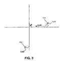
- Antifuse 12is shown programmed in the schematic drawing illustrated in FIG. 3 . As also shown in FIG. 3 , as current flows through the ruptured dielectric of antifuse 12 , the resistance level drops. This is referred to by those skilled in the art as soaking.
- FIG. 4is a schematic diagram illustrating the problems inherent in concurrent programming of antifuses in the prior art.
- Antifuses 52 and 54are the fuses to be programmed.
- Antifuses 56 and 58are not to be programmed. Based on the programming algorithm set forth above, vertical routing tracks 60 and 62 are charged to Vpp and horizontal routing tracks 64 and 66 are pulled down to ground.
- Antifuses 52 and 54will see full Vpp across the dielectric and rupture. However, while antifuses 56 and 58 are not to be programmed, they will also have full Vpp stress across the dielectric and may be programmed despite the intention that they not be programmed.
- an antifuse FPGAthe antifuses in the FPGA are programmed one at time. As the size of the FPGA increases, the number of antifuses becomes much greater and the programming time increases. Hence, there is a need for an antifuse FPGA with a shorter programming time. Thus, there is also a need for an antifuse FPGA in which the antifuses to be programmed can be concurrently programmed.
- the present inventioncomprises an FPGA having a plurality of logic modules with programmable elements.
- the logic modulesare partitioned into a plurality of individually programmable groups and an isolation device may be coupled between the individually programmable groups of logic modules such that each of the programmable elements in each of the plurality of individually programmable logic modules may be programmed simultaneously.
- the present inventionalso comprises a method of programming a plurality of tiles in an FPGA comprising loading the address data identifying which antifuses in tiles 1 through N are to be programmed. Next, from the loaded address data, one antifuse is selected in each of tiles 1 through N that need to be programmed. Then, the selected antifuses in each of the tiles 1 through N are programmed. Next, it is determined whether all the antifuses in tiles 1 through N are programmed. If all the antifuses in tiles 1 through N are not programmed, the software module selects from the loaded addresses the next one antifuse in each tile 1 through N that needs to be programmed. Finally, if all the antifuses are programmed in tiles 1 through N, the program ends.
- FIG. 1is a schematic diagram of an antifuse programming circuit before programming.
- FIG. 2is a schematic diagram of an antifuse circuit programming path prior to programming.
- FIG. 3is a schematic diagram of an antifuse circuit programming path after programming.
- FIG. 4is a schematic diagram of a prior art antifuse FPGA circuit illustrating problems with attempted concurrent programming.
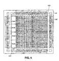
- FIG. 5is a simplified block diagram of a tile of an antifuse FPGA of the present system.
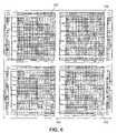
- FIG. 6is a simplified block diagram an antifuse FPGA comprising four tiles of the present system.
- FIG. 7is a schematic diagram of the programming circuit of the current system.
- FIG. 8is a schematic diagram illustrating an embodiment of an isolation device of the present system.
- FIG. 9is a schematic diagram illustrating another embodiment of an isolation device of the present system.
- FIG. 10is a schematic diagram illustrating yet another embodiment of an isolation device of the present system.
- FIG. 11is a simplified block diagram of an antifuse FPGA tile 200 with a long shift register (LSR).
- LSRlong shift register
- FIG. 12is a flowchart illustrating a method of programming as disclosed in the present system.
- FIG. 13is a flowchart illustrating another method of programming as disclosed in the present system.
- FIG. 5is a simplified block diagram of an example of a core tile 100 of an antifuse FPGA of the present invention.
- Core tile 100comprises an array of logic modules 102 and a column of RAM modules 104 .
- An FPGAcan be built from a single core tile 100 , surrounded by columns and rows of I/O modules as illustrated in FIG. 5 or as illustrated in FIG. 6 as an antifuse FPGA of the having four or more core tiles 100 .
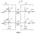
- FIG. 7is a schematic diagram illustrating the concurrently programmable antifuse FPGA 200 of the current system.
- Antifuse FPGA 200 of the current systemis partitioned into several programming independent tiles illustrated in FIGS. 5 , and 7 by reference numeral 100 .
- antifuses 170 and 174are located in a first core tile 100 .
- Antifuses 172 and 176are located in a second core tile 100 .
- core tiles 100are treated as isolated tiles.
- Core tilesare isolated during the programming of the antifuse FPGA by isolation devices 186 and 188 .
- antifuses 170 and 172are the fuses to be programmed.
- Antifuses 174 and 176are the fuses not to be programmed.
- isolation devicesillustrated by reference numerals 186 and 188 , are shown as open switches.
- isolation device 188divides horizontal track 182 into isolated portions 182 a and 182 b while isolation device 186 divides horizontal track 184 into isolated portions 184 a and 184 b .
- Antifuse 170is programmed by applying Vpp to vertical routing track 178 and pulling horizontal routing track 184 b to ground.
- Antifuse 174will remain unprogrammed because Vpp/2 is applied to horizontal routing track 182 b .
- Antifuse 172is programmed by applying Vpp to vertical routing track 180 and pulling horizontal routing track 182 a to ground. Antifuse 176 will remain unprogrammed because Vpp/2 is applied to horizontal routing track 184 a . Thus, during programming, each tile can be treated as a separate device, allowing the programming of one antifuse in each tile concurrently, instead of consecutively, and providing a much faster programming environment.
- FIG. 8illustrates a schematic of one embodiment of an isolation device 202 between tiles 100 .
- Isolation device 202partitions horizontal routing track 204 into isolated horizontal routing tracks 204 a and 204 b .
- Isolation device 202is a transistor (referred to hereinafter as isolation transistor 202 ) with its source/drain bridging horizontal routing tracks 204 a and 204 b .
- Isolation transistor 202has a gate that is driven by a voltage that is approximately two volts higher than the core operating voltage by an external source or the voltage can be generated by a built-in pump circuit, well known to those of ordinary skill in the art, which generates a PMPOUT signal to control the gate of isolation transistor 202 .
- PMPOUT signalcan be set as a logical high or low during programming/testing.
- Isolation device 202separates signals on horizontal routing tracks 204 a and 204 b when the PMPOUT signal is set at logical low. For normal operation, PMPOUT is always set at logical high such that isolation transistor becomes conductive and joins horizontal routing tracks 204 a and 204 b together.
- FIG. 9illustrates another embodiment of an isolation device 210 .
- Isolation device 210is a single isolation antifuse referred to hereinafter as isolation antifuse 210 .
- Isolation antifuse 210partitions horizontal routing track 212 into isolated horizontal routing tracks 212 a and 212 b .
- Isolation antifuse 210bridges horizontal routing tracks 212 a and 212 b .
- isolation antifuse 210is ruptured it is nonconductive and separates the signals between horizontal routing tracks 212 a and 212 b .
- isolation antifuse 210is programmed to connect tiles 100 and horizontal routing tracks 212 a and 212 b .
- isolation devicesmay be programmed making a particular track between tiles conductive or left unprogrammed, leaving a particular track between tiles unconnected.
- FIG. 10is a schematic diagram illustrating yet another embodiment of isolation device 220 .
- Isolation device 220partitions horizontal routing track 230 into isolated portions 230 a and 230 b and also isolating tiles 100 .
- Isolation device 220comprises antifuses 222 and 224 coupled together through pull-down transistor 226 .
- Pull-down transistor 226enables programming of fuses 222 and 224 after programming the user circuit in the antifuse FPGA of the present system to connect horizontal routing track 230 into isolated portions 230 a and 230 b and isolating tiles 100 .
- each tilecan be treated as a separate device, allowing the programming of one antifuse in each tile concurrently, instead of consecutively, and providing a much faster programming environment.
- the tile level or local control signalsare controlled by a bit pattern loaded into a tile mode register.
- Registerswhich store data temporarily, are well known to those skilled in the art and will not be discussed herein in order to avoid complicating and obscuring the present disclosure. All tile mode registers in an antifuse FPGA of the present system can be loaded with different bit-patterns to produce different circuits.
- all tile mode registersmay be loaded with the same bit-pattern with “broadcast mode.” Broadcast mode is very practical for the testing of an unprogrammed antifuse FPGA, so that all tile level controls are set to act the same way, and thus produce the same value.
- FIG. 11is a simplified block diagram of an antifuse FPGA tile 100 (as shown in FIG. 5 ) with a long shift register (LSR) 301 .
- Long shift register 301is divided into six peripheries 302 , 304 , 306 , 308 , 310 and 312 .
- Tile 300is divided into four quadrants 314 , 316 , 318 and 320 surrounded by the six peripheries 302 , 304 , 306 , 308 , 310 and 312 of LSR 301 .
- LSR 301 peripheries 302 , 304 , 306 , 308 , 310 and 312are used for testing and programming the device.
- register bits and their associated circuitsgenerate the antifuse addressing, regional testing and programming controls.
- the register bitsare chained together within each periphery and between peripheries to form LSR 301 .
- the address of an antifuse being programmed (FBP)is loaded into LSR 301 .
- the LSR bits belonging to any of the six peripheries as a groupcan be skipped by setting the appropriate values of the “skip” controls. For example, when all skip controls are set to “1”, all the LSR bits of the tile will be skipped.
- the “skip” functioncan be used for one or multiple peripheries. Partial skip is useful when a portion of the fuse address bit is the same. Skipping the whole tile is useful when debugging during a circuit failure.
- An antifuse FPGAmay contain a global mode register.
- Global mode registersare well known to those skilled in the art and will not be discussed herein in order to avoid complicating the present disclosure.
- the bit pattern loaded into a global mode register of an antifuse FPGA of the present systemsets the chip level controls.
- the broadcast modeis enabled when the “DRBCT” bit in the global mode register is set.
- the broadcast modeis enabled, the same pattern is loaded into all tile level tile mode registers and LSRs. This function is useful for testing unprogrammed FPGAs and allows for parallel testing of all tiles in a chip simultaneously.
- Vpp pinsexternal programming voltage power supply pins
- Vppis set at 5 volts and capable of sourcing more than 20 mA.
- Vcc2.55-3.3V
- the GMR control signalis set to “VPPHH”, all the internal Vpp pins are tied together for parallel testing.
- Each tilemay also include a single bit mask register.
- Mask registersare well known to those skilled in the art and will not be discussed herein in order to avoid complicating the present disclosure.
- the mask register bitWhen the mask register bit is set, the Vpp voltage is applied to all FBP in each tile and Vpp/2 is applied to all other antifuses in the FPGA.
- the mask register bitWhen the mask register bit is reset, it prevents the Vpp pulse from reaching the FBP so that the FBPs in each tile are not being reprogrammed.
- parallel programming an antifuse FPGAfor a given group of tiles, one antifuse per tile may be programmed at the same time.
- the present inventionmay be applied to an antifuse-based memory array.
- the memory arrayis divided into individually programmable groups and then isolation devices are inserted in the circuit between the individually programmable memory array modules.
- FIG. 12is a flowchart illustrating a method of programming as disclosed in the present system.
- a software module stored on a user's computer systemmay perform the disclosed method.
- the software moduleloads the address data identifying which antifuses in tiles 1 through N are to be programmed.
- the address data for the antifuses to be programmedare selected according to a netlist defined by an individual user circuit. Each user circuit may be unique and thus every netlist may define different antifuses in different tiles to be programmed.
- an FPGAmay be partitioned into any number of tiles as well as just having one tile.
- the software moduleselects one antifuse in each of tiles 1 through N that needs to be programmed at act 352 .
- the software moduleprograms the selected antifuses concurrently in each of the tiles 1 through N.
- it is determined from the loaded address datawhether all the antifuses that need to be programmed in tiles 1 through N have been programmed. If all the antifuses designated for programming in tiles 1 through N are not programmed, the software module returns to act 352 and selects from the loaded addresses the next one antifuse in each tile 1 through N that needs to be programmed. As one skilled in the art having the benefit of this disclosure will realize, not all tiles will have the same number of fuses to be programmed.
- tile 1may have one hundred fuses to be programmed while tile two may have one hundred and fifty antifuses to be programmed.
- tile twomay have one hundred and fifty antifuses to be programmed.
- FIG. 13is a flowchart illustrating another method of programming 400 as disclosed in the present system.
- a software module stored on the user's systemperforms the disclosed method.
- the software moduleloads the address data identifying which antifuses in each of tiles 1 through N are to be programmed.
- the address data for the antifuses to be programmedare selected according to a netlist defined by an individual user circuit. Each user circuit may be unique and thus every netlist may define different antifuses in different tiles to be programmed.
- an FPGAmay be partitioned into any number of tiles as well as just having one tile.
- the software moduleselects one antifuse whose mask bits are set in each of tiles 1 through N to be programmed.
- the software moduleprograms the selected antifuses concurrently in tiles 1 through N.
- the software moduledetermines whether the selected antifuses in each of tiles 1 through N have been programmed. If the selected antifuse has not been completely programmed, the software module continues to program the selected antifuse at act 410 .
- the software moduleresets the mask register bit while simultaneously soaking the previously selected antifuses in tiles 1 through N.
- the software moduledetermines whether all antifuses designated for programming have been programmed.
- tile 1may have one hundred fuses to be programmed while tile two may have one hundred and fifty antifuses to be programmed.
- tile 1may have one hundred fuses to be programmed while tile two may have one hundred and fifty antifuses to be programmed.
- tile twomay have one hundred and fifty antifuses to be programmed.
- not all tileswill have antifuses to be programmed during the entire parallel programming process.
- the software modulereturns to act 352 and selects from the loaded addresses the next one antifuse in each tile 1 through N that needs to be programmed. Finally, if all the antifuses designated for programming have been programmed in tiles 1 through N, the program ends at act 358 .
- the above method of programmingmay be applied to antifuse memory arrays using the same steps as set forth above applicable to logic arrays.
Landscapes
- Physics & Mathematics (AREA)
- Engineering & Computer Science (AREA)
- Mathematical Physics (AREA)
- Computer Hardware Design (AREA)
- General Engineering & Computer Science (AREA)
- Computing Systems (AREA)
- Theoretical Computer Science (AREA)
- Evolutionary Computation (AREA)
- Geometry (AREA)
- General Physics & Mathematics (AREA)
- Design And Manufacture Of Integrated Circuits (AREA)
- Logic Circuits (AREA)
Abstract
Description
Ttotal=Toh+ΣTfuse
Claims (5)
Priority Applications (2)
| Application Number | Priority Date | Filing Date | Title |
|---|---|---|---|
| US11/532,757US7269814B1 (en) | 2002-10-08 | 2006-09-18 | Parallel programmable antifuse field programmable gate array device (FPGA) and a method for programming and testing an antifuse FPGA |
| US11/837,700US7549138B2 (en) | 2002-10-08 | 2007-08-13 | Parallel programmable antifuse field programmable gate array device (FPGA) and a method for programming and testing an antifuse FPGA |
Applications Claiming Priority (3)
| Application Number | Priority Date | Filing Date | Title |
|---|---|---|---|
| US10/267,917US6885218B1 (en) | 2002-10-08 | 2002-10-08 | Parallel programmable antifuse field programmable gate array device (FPGA) and a method for programming and testing an antifuse FPGA |
| US10/833,608US7111272B1 (en) | 2002-10-08 | 2004-04-27 | Parallel programmable antifuse field programmable gate array device (FPGA) and a method for programming and testing an antifuse FPGA |
| US11/532,757US7269814B1 (en) | 2002-10-08 | 2006-09-18 | Parallel programmable antifuse field programmable gate array device (FPGA) and a method for programming and testing an antifuse FPGA |
Related Parent Applications (1)
| Application Number | Title | Priority Date | Filing Date |
|---|---|---|---|
| US10/833,608ContinuationUS7111272B1 (en) | 2002-10-08 | 2004-04-27 | Parallel programmable antifuse field programmable gate array device (FPGA) and a method for programming and testing an antifuse FPGA |
Related Child Applications (1)
| Application Number | Title | Priority Date | Filing Date |
|---|---|---|---|
| US11/837,700ContinuationUS7549138B2 (en) | 2002-10-08 | 2007-08-13 | Parallel programmable antifuse field programmable gate array device (FPGA) and a method for programming and testing an antifuse FPGA |
Publications (1)
| Publication Number | Publication Date |
|---|---|
| US7269814B1true US7269814B1 (en) | 2007-09-11 |
Family
ID=38473375
Family Applications (2)
| Application Number | Title | Priority Date | Filing Date |
|---|---|---|---|
| US11/532,757Expired - Fee RelatedUS7269814B1 (en) | 2002-10-08 | 2006-09-18 | Parallel programmable antifuse field programmable gate array device (FPGA) and a method for programming and testing an antifuse FPGA |
| US11/837,700Expired - Fee RelatedUS7549138B2 (en) | 2002-10-08 | 2007-08-13 | Parallel programmable antifuse field programmable gate array device (FPGA) and a method for programming and testing an antifuse FPGA |
Family Applications After (1)
| Application Number | Title | Priority Date | Filing Date |
|---|---|---|---|
| US11/837,700Expired - Fee RelatedUS7549138B2 (en) | 2002-10-08 | 2007-08-13 | Parallel programmable antifuse field programmable gate array device (FPGA) and a method for programming and testing an antifuse FPGA |
Country Status (1)
| Country | Link |
|---|---|
| US (2) | US7269814B1 (en) |
Cited By (3)
| Publication number | Priority date | Publication date | Assignee | Title |
|---|---|---|---|---|
| US20080028354A1 (en)* | 2002-10-08 | 2008-01-31 | Actel Corporation | Parallel programmable antifuse field programmable gate array device (fpga) and a method for programming and testing an antifuse fpga |
| CN103064810A (en)* | 2011-10-18 | 2013-04-24 | 上海航天控制工程研究所 | Method of achieving satellite serial port communication |
| CN103163450A (en)* | 2011-12-16 | 2013-06-19 | 中国科学院微电子研究所 | Navigation mapping method applied to testing of FPGA with specific structure |
Citations (2)
| Publication number | Priority date | Publication date | Assignee | Title |
|---|---|---|---|---|
| US5777887A (en)* | 1995-05-12 | 1998-07-07 | Crosspoint Solutions, Inc. | FPGA redundancy |
| US6727726B1 (en)* | 2002-11-12 | 2004-04-27 | Actel Corporation | Field programmable gate array architecture including a buffer module and a method of distributing buffer modules in a field programmable gate array |
Family Cites Families (155)
| Publication number | Priority date | Publication date | Assignee | Title |
|---|---|---|---|---|
| US4255748A (en) | 1979-02-12 | 1981-03-10 | Automation Systems, Inc. | Bus fault detector |
| NL8001452A (en) | 1980-03-12 | 1981-10-01 | Philips Nv | SECURE CURRENT MEASUREMENT. |
| US4772812A (en) | 1981-07-27 | 1988-09-20 | Data General Corporation | Tri-state output buffer circuit including a capacitor and dynamic depletion mode switching device |
| US4717912A (en) | 1982-10-07 | 1988-01-05 | Advanced Micro Devices, Inc. | Apparatus for producing any one of a plurality of signals at a single output |
| US4870302A (en) | 1984-03-12 | 1989-09-26 | Xilinx, Inc. | Configurable electrical circuit having configurable logic elements and configurable interconnects |
| US4625313A (en) | 1984-07-06 | 1986-11-25 | Tektronix, Inc. | Method and apparatus for testing electronic equipment |
| US4713557A (en) | 1984-09-26 | 1987-12-15 | Xilinx, Inc. | Bidirectional buffer amplifier |
| US4706216A (en) | 1985-02-27 | 1987-11-10 | Xilinx, Inc. | Configurable logic element |
| US4684830A (en) | 1985-03-22 | 1987-08-04 | Monolithic Memories, Inc. | Output circuit for a programmable logic array |
| US5225719A (en) | 1985-03-29 | 1993-07-06 | Advanced Micro Devices, Inc. | Family of multiple segmented programmable logic blocks interconnected by a high speed centralized switch matrix |
| US4742252A (en) | 1985-03-29 | 1988-05-03 | Advanced Micro Devices, Inc. | Multiple array customizable logic device |
| US4638243A (en) | 1985-06-05 | 1987-01-20 | Monolithic Memories, Inc. | Short detector for fusible link array using single reference fuse |
| US4638187A (en) | 1985-10-01 | 1987-01-20 | Vtc Incorporated | CMOS output buffer providing high drive current with minimum output signal distortion |
| US4718042A (en) | 1985-12-23 | 1988-01-05 | Ncr Corporation | Non-destructive method and circuit to determine the programmability of a one time programmable device |
| JPS6341048A (en) | 1986-08-06 | 1988-02-22 | Mitsubishi Electric Corp | Standard cell type large scale integrated circuit |
| US5208530A (en) | 1986-09-19 | 1993-05-04 | Actel Corporation | Testability architecture and techniques for programmable interconnect architecture |
| US4857774A (en) | 1986-09-19 | 1989-08-15 | Actel Corporation | Testing apparatus and diagnostic method for use with programmable interconnect architecture |
| US5223792A (en) | 1986-09-19 | 1993-06-29 | Actel Corporation | Testability architecture and techniques for programmable interconnect architecture |
| US5365165A (en) | 1986-09-19 | 1994-11-15 | Actel Corporation | Testability architecture and techniques for programmable interconnect architecture |
| US4758745B1 (en) | 1986-09-19 | 1994-11-15 | Actel Corp | User programmable integrated circuit interconnect architecture and test method |
| US5341092A (en) | 1986-09-19 | 1994-08-23 | Actel Corporation | Testability architecture and techniques for programmable interconnect architecture |
| US5309091A (en) | 1986-09-19 | 1994-05-03 | Actel Corporation | Testability architecture and techniques for programmable interconnect architecture |
| US5083083A (en) | 1986-09-19 | 1992-01-21 | Actel Corporation | Testability architecture and techniques for programmable interconnect architecture |
| US5451887A (en) | 1986-09-19 | 1995-09-19 | Actel Corporation | Programmable logic module and architecture for field programmable gate array device |
| JPS63299251A (en) | 1987-05-29 | 1988-12-06 | Toshiba Corp | Manufacture of semiconductor device |
| US5046035A (en) | 1987-08-26 | 1991-09-03 | Ict International Cmos Tech., Inc. | High-performance user programmable logic device (PLD) |
| JP2619448B2 (en) | 1987-12-24 | 1997-06-11 | 富士通株式会社 | Digital phase comparator |
| US5258319A (en) | 1988-02-19 | 1993-11-02 | Mitsubishi Denki Kabushiki Kaisha | Method of manufacturing a MOS type field effect transistor using an oblique ion implantation step |
| US4935645A (en) | 1988-03-02 | 1990-06-19 | Dallas Semiconductor Corporation | Fusing and detection circuit |
| US4930097A (en) | 1988-12-30 | 1990-05-29 | Intel Corporation | Architecture for an improved performance of a programmable logic device |
| US4959561A (en) | 1989-01-04 | 1990-09-25 | Motorola, Inc. | MOS output buffer with reduced supply line disturbance |
| US5008855A (en) | 1989-07-18 | 1991-04-16 | Actel Corporation | Method of programming anti-fuse element |
| US5400262A (en) | 1989-09-20 | 1995-03-21 | Aptix Corporation | Universal interconnect matrix array |
| US4978905A (en) | 1989-10-31 | 1990-12-18 | Cypress Semiconductor Corp. | Noise reduction output buffer |
| US5121394A (en) | 1989-12-20 | 1992-06-09 | Bull Hn Information Systems Inc. | Method of organizing programmable logic array devices for board testability |
| US5198705A (en) | 1990-05-11 | 1993-03-30 | Actel Corporation | Logic module with configurable combinational and sequential blocks |
| US5126282A (en) | 1990-05-16 | 1992-06-30 | Actel Corporation | Methods of reducing anti-fuse resistance during programming |
| US5191241A (en) | 1990-08-01 | 1993-03-02 | Actel Corporation | Programmable interconnect architecture |
| US5132571A (en) | 1990-08-01 | 1992-07-21 | Actel Corporation | Programmable interconnect architecture having interconnects disposed above function modules |
| US5144166A (en) | 1990-11-02 | 1992-09-01 | Concurrent Logic, Inc. | Programmable logic cell and array |
| US5367207A (en) | 1990-12-04 | 1994-11-22 | Xilinx, Inc. | Structure and method for programming antifuses in an integrated circuit array |
| US5222066A (en) | 1990-12-26 | 1993-06-22 | Motorola, Inc. | Modular self-test for embedded SRAMS |
| US5122685A (en) | 1991-03-06 | 1992-06-16 | Quicklogic Corporation | Programmable application specific integrated circuit and logic cell therefor |
| US5220213A (en) | 1991-03-06 | 1993-06-15 | Quicklogic Corporation | Programmable application specific integrated circuit and logic cell therefor |
| US5701027A (en) | 1991-04-26 | 1997-12-23 | Quicklogic Corporation | Programmable interconnect structures and programmable integrated circuits |
| JP3014164B2 (en) | 1991-05-15 | 2000-02-28 | 沖電気工業株式会社 | Output buffer circuit |
| US5221865A (en) | 1991-06-21 | 1993-06-22 | Crosspoint Solutions, Inc. | Programmable input/output buffer circuit with test capability |
| US5187392A (en) | 1991-07-31 | 1993-02-16 | Intel Corporation | Programmable logic device with limited signal swing |
| US5302546A (en) | 1991-07-31 | 1994-04-12 | Quicklogic Corporation | Programming of antifuses |
| US5550782A (en) | 1991-09-03 | 1996-08-27 | Altera Corporation | Programmable logic array integrated circuits |
| US5260610A (en) | 1991-09-03 | 1993-11-09 | Altera Corporation | Programmable logic element interconnections for programmable logic array integrated circuits |
| US5883850A (en) | 1991-09-03 | 1999-03-16 | Altera Corporation | Programmable logic array integrated circuits |
| US5208491A (en) | 1992-01-07 | 1993-05-04 | Washington Research Foundation | Field programmable gate array |
| US5220215A (en) | 1992-05-15 | 1993-06-15 | Micron Technology, Inc. | Field programmable logic array with two or planes |
| US5300830A (en) | 1992-05-15 | 1994-04-05 | Micron Semiconductor, Inc. | Programmable logic device macrocell with an exclusive feedback and exclusive external input lines for registered and combinatorial modes using a dedicated product term for control |
| FR2691307A1 (en) | 1992-05-18 | 1993-11-19 | Lausanne Ecole Polytechnique F | An intermediate circuit between a low voltage logic circuit and a high voltage output stage realized in standard CMOS technology. |
| US5272388A (en) | 1992-06-09 | 1993-12-21 | Actel Corporation | High-yield methods for programming antifuses |
| US5286922A (en) | 1992-07-14 | 1994-02-15 | Curtiss Thomas E | Fluorescent coated wire |
| US5646547A (en) | 1994-04-28 | 1997-07-08 | Xilinx, Inc. | Logic cell which can be configured as a latch without static one's problem |
| US5304871A (en) | 1992-07-24 | 1994-04-19 | Actel Corporation | Programmable interconnect architecture employing leaky programmable elements |
| DE4224804C1 (en) | 1992-07-27 | 1994-01-13 | Siemens Ag | Programmable logic circuitry |
| US5294846A (en) | 1992-08-17 | 1994-03-15 | Paivinen John O | Method and apparatus for programming anti-fuse devices |
| US5317698A (en) | 1992-08-18 | 1994-05-31 | Actel Corporation | FPGA architecture including direct logic function circuit to I/O interconnections |
| US5293133A (en) | 1992-08-27 | 1994-03-08 | Quicklogic Corporation | Method of determining an electrical characteristic of an antifuse and apparatus therefor |
| GB9223226D0 (en) | 1992-11-05 | 1992-12-16 | Algotronix Ltd | Improved configurable cellular array (cal ii) |
| US5300832A (en) | 1992-11-10 | 1994-04-05 | Sun Microsystems, Inc. | Voltage interfacing buffer with isolation transistors used for overvoltage protection |
| US5809281A (en) | 1993-03-30 | 1998-09-15 | Altera Corporation | Field programmable gate array with high speed SRAM based configurable function block configurable as high performance logic or block of SRAM |
| JPH0774616A (en) | 1993-07-06 | 1995-03-17 | Seiko Epson Corp | Signal voltage level conversion circuit and output buffer circuit |
| US5394033A (en) | 1993-09-01 | 1995-02-28 | Lattice Semiconductor Corporation | Structure and method for implementing hierarchical routing pools in a programmable logic circuit |
| US5396128A (en) | 1993-09-13 | 1995-03-07 | Motorola, Inc. | Output circuit for interfacing integrated circuits having different power supply potentials |
| US5375089A (en) | 1993-10-05 | 1994-12-20 | Advanced Micro Devices, Inc. | Plural port memory system utilizing a memory having a read port and a write port |
| US5399920A (en) | 1993-11-09 | 1995-03-21 | Texas Instruments Incorporated | CMOS driver which uses a higher voltage to compensate for threshold loss of the pull-up NFET |
| US5365485A (en) | 1993-11-22 | 1994-11-15 | Texas Instruments Incorporated | Fifo with fast retransmit mode |
| US5486775A (en) | 1993-11-22 | 1996-01-23 | Altera Corporation | Multiplexer structures for use in making controllable interconnections in integrated circuits. |
| US5455525A (en) | 1993-12-06 | 1995-10-03 | Intelligent Logic Systems, Inc. | Hierarchically-structured programmable logic array and system for interconnecting logic elements in the logic array |
| US5430687A (en) | 1994-04-01 | 1995-07-04 | Xilinx, Inc. | Programmable logic device including a parallel input device for loading memory cells |
| US5689195A (en) | 1995-05-17 | 1997-11-18 | Altera Corporation | Programmable logic array integrated circuit devices |
| US5424655A (en)* | 1994-05-20 | 1995-06-13 | Quicklogic Corporation | Programmable application specific integrated circuit employing antifuses and methods therefor |
| US5469396A (en) | 1994-06-07 | 1995-11-21 | Actel Corporation | Apparatus and method determining the resistance of antifuses in an array |
| TW265489B (en) | 1994-07-20 | 1995-12-11 | Micron Technology Inc | Low-to-high voltage cmos driver circuit for driving capacitive loads |
| US5761099A (en) | 1994-11-04 | 1998-06-02 | Altera Corporation | Programmable logic array integrated circuits with enhanced carry routing |
| US5495181A (en) | 1994-12-01 | 1996-02-27 | Quicklogic Corporation | Integrated circuit facilitating simultaneous programming of multiple antifuses |
| GB2297409B (en) | 1995-01-27 | 1998-08-19 | Altera Corp | Programmable logic devices |
| US5537057A (en) | 1995-02-14 | 1996-07-16 | Altera Corporation | Programmable logic array device with grouped logic regions and three types of conductors |
| US5847577A (en) | 1995-02-24 | 1998-12-08 | Xilinx, Inc. | DRAM memory cell for programmable logic devices |
| US5594363A (en) | 1995-04-07 | 1997-01-14 | Zycad Corporation | Logic cell and routing architecture in a field programmable gate array |
| US5850564A (en) | 1995-05-03 | 1998-12-15 | Btr, Inc, | Scalable multiple level tab oriented interconnect architecture |
| US5640106A (en) | 1995-05-26 | 1997-06-17 | Xilinx, Inc. | Method and structure for loading data into several IC devices |
| US5835165A (en) | 1995-06-07 | 1998-11-10 | Lsi Logic Corporation | Reduction of false locking code words in concatenated decoders |
| US5838954A (en) | 1995-08-18 | 1998-11-17 | Xilinx, Inc. | Computer-implemented method of optimizing a time multiplexed programmable logic device |
| US5701441A (en) | 1995-08-18 | 1997-12-23 | Xilinx, Inc. | Computer-implemented method of optimizing a design in a time multiplexed programmable logic device |
| US5546019A (en) | 1995-08-24 | 1996-08-13 | Taiwan Semiconductor Manufacture Company | CMOS I/O circuit with 3.3 volt output and tolerance of 5 volt input |
| US5666322A (en) | 1995-09-21 | 1997-09-09 | Nec Electronics, Inc. | Phase-locked loop timing controller in an integrated circuit memory |
| US5815004A (en) | 1995-10-16 | 1998-09-29 | Xilinx, Inc. | Multi-buffered configurable logic block output lines in a field programmable gate array |
| US5744991A (en) | 1995-10-16 | 1998-04-28 | Altera Corporation | System for distributing clocks using a delay lock loop in a programmable logic circuit |
| US5600264A (en) | 1995-10-16 | 1997-02-04 | Xilinx, Inc. | Programmable single buffered six pass transistor configuration |
| US5880492A (en) | 1995-10-16 | 1999-03-09 | Xilinx, Inc. | Dedicated local line interconnect layout |
| US5848006A (en) | 1995-12-06 | 1998-12-08 | Nec Corporation | Redundant semiconductor memory device using a single now address decoder for driving both sub-wordlines and redundant sub-wordlines |
| US5914906A (en) | 1995-12-20 | 1999-06-22 | International Business Machines Corporation | Field programmable memory array |
| US5870586A (en) | 1996-01-31 | 1999-02-09 | Xilinx, Inc. | Configuration emulation of a programmable logic device |
| US5744980A (en) | 1996-02-16 | 1998-04-28 | Actel Corporation | Flexible, high-performance static RAM architecture for field-programmable gate arrays |
| GB9604496D0 (en) | 1996-03-01 | 1996-05-01 | Xilinx Inc | Embedded memory for field programmable gate array |
| US5835998A (en) | 1996-04-04 | 1998-11-10 | Altera Corporation | Logic cell for programmable logic devices |
| US5847441A (en) | 1996-05-10 | 1998-12-08 | Micron Technology, Inc. | Semiconductor junction antifuse circuit |
| US5742181A (en) | 1996-06-04 | 1998-04-21 | Hewlett-Packard Co. | FPGA with hierarchical interconnect structure and hyperlinks |
| US5852608A (en) | 1996-06-06 | 1998-12-22 | Sun Microsystems, Inc. | Structure and method for bi-directional data transfer between asynchronous clock domains |
| US5828538A (en) | 1996-06-21 | 1998-10-27 | Quicklogic Corporation | Power-up circuit for field programmable gate arrays |
| US5825201A (en) | 1996-06-21 | 1998-10-20 | Quicklogic Corporation | Programming architecture for a programmable integrated circuit employing antifuses |
| US5952847A (en) | 1996-06-25 | 1999-09-14 | Actel Corporation | Multiple logic family compatible output driver |
| US5870327A (en) | 1996-07-19 | 1999-02-09 | Xilinx, Inc. | Mixed mode RAM/ROM cell using antifuses |
| US6034547A (en) | 1996-09-04 | 2000-03-07 | Advantage Logic, Inc. | Method and apparatus for universal program controlled bus |
| US5859544A (en) | 1996-09-05 | 1999-01-12 | Altera Corporation | Dynamic configurable elements for programmable logic devices |
| US5880597A (en) | 1996-09-18 | 1999-03-09 | Altera Corporation | Interleaved interconnect for programmable logic array devices |
| US5825202A (en) | 1996-09-26 | 1998-10-20 | Xilinx, Inc. | Integrated circuit with field programmable and application specific logic areas |
| US5832892A (en) | 1996-10-11 | 1998-11-10 | Yaoita; Yasuhito | Spark ignition internal combustion engine |
| US5883526A (en) | 1997-04-17 | 1999-03-16 | Altera Corporation | Hierarchical interconnect for programmable logic devices |
| US5828230A (en) | 1997-01-09 | 1998-10-27 | Xilinx, Inc. | FPGA two turn routing structure with lane changing and minimum diffusion area |
| US5880598A (en) | 1997-01-10 | 1999-03-09 | Xilinx, Inc. | Tile-based modular routing resources for high density programmable logic device |
| US5821776A (en) | 1997-01-31 | 1998-10-13 | Actel Corporation | Field programmable gate array with mask programmed analog function circuits |
| US5854763A (en) | 1997-01-31 | 1998-12-29 | Mosaid Technologies Inc. | Integrated circuit with non-binary decoding and data access |
| US6011744A (en) | 1997-07-16 | 2000-01-04 | Altera Corporation | Programmable logic device with multi-port memory |
| JP3085258B2 (en) | 1997-09-10 | 2000-09-04 | 日本電気株式会社 | Clock signal distribution circuit |
| US5991908A (en)* | 1997-09-29 | 1999-11-23 | Xilinx, Inc. | Boundary scan chain with dedicated programmable routing |
| US6100715A (en) | 1998-12-15 | 2000-08-08 | Vantis Corporation | Methods for configuring FPGA's having variable grain blocks and logic for providing time-shared access to interconnect resources |
| US6034677A (en) | 1997-10-17 | 2000-03-07 | Sony Corporation | Method and apparatus for displaying an electronic program guide |
| JPH11205102A (en) | 1998-01-13 | 1999-07-30 | Mitsubishi Electric Corp | Delay synchronization circuit |
| US6038627A (en) | 1998-03-16 | 2000-03-14 | Actel Corporation | SRAM bus architecture and interconnect to an FPGA |
| US6049487A (en) | 1998-03-16 | 2000-04-11 | Actel Corporation | Embedded static random access memory for field programmable gate array |
| US6292925B1 (en) | 1998-03-27 | 2001-09-18 | Xilinx, Inc. | Context-sensitive self implementing modules |
| US6260182B1 (en) | 1998-03-27 | 2001-07-10 | Xilinx, Inc. | Method for specifying routing in a logic module by direct module communication |
| US6216258B1 (en) | 1998-03-27 | 2001-04-10 | Xilinx, Inc. | FPGA modules parameterized by expressions |
| US6289068B1 (en) | 1998-06-22 | 2001-09-11 | Xilinx, Inc. | Delay lock loop with clock phase shifter |
| US6169416B1 (en)* | 1998-09-01 | 2001-01-02 | Quicklogic Corporation | Programming architecture for field programmable gate array |
| JP3993717B2 (en) | 1998-09-24 | 2007-10-17 | 富士通株式会社 | Semiconductor integrated circuit device |
| US6157213A (en) | 1998-10-19 | 2000-12-05 | Xilinx, Inc. | Layout architecture and method for fabricating PLDs including multiple discrete devices formed on a single chip |
| US6242943B1 (en) | 1998-12-31 | 2001-06-05 | Khaled Ahmad El-Ayat | Programmable multi-standard I/O architecture for FPGAS |
| US6177844B1 (en) | 1999-01-08 | 2001-01-23 | Altera Corporation | Phase-locked loop or delay-locked loop circuitry for programmable logic devices |
| US6519753B1 (en)* | 1999-11-30 | 2003-02-11 | Quicklogic Corporation | Programmable device with an embedded portion for receiving a standard circuit design |
| US6353334B1 (en) | 2000-01-27 | 2002-03-05 | Xilinx, Inc. | Circuit for converting a logic signal on an output node to a pair of low-voltage differential signals |
| US6535043B2 (en) | 2000-05-26 | 2003-03-18 | Lattice Semiconductor Corp | Clock signal selection system, method of generating a clock signal and programmable clock manager including same |
| US6418059B1 (en) | 2000-06-26 | 2002-07-09 | Intel Corporation | Method and apparatus for non-volatile memory bit sequence program controller |
| US6751723B1 (en)* | 2000-09-02 | 2004-06-15 | Actel Corporation | Field programmable gate array and microcontroller system-on-a-chip |
| US6570805B2 (en)* | 2000-12-20 | 2003-05-27 | Actel Corporation | Antifuse memory cell and antifuse memory cell array |
| US6501295B1 (en) | 2001-06-01 | 2002-12-31 | Sun Microsystems, Inc. | Overdriven pass transistors |
| US6891394B1 (en)* | 2002-06-04 | 2005-05-10 | Actel Corporation | Field-programmable gate array low voltage differential signaling driver utilizing two complimentary output buffers |
| US6750674B1 (en)* | 2002-10-02 | 2004-06-15 | Actel Corporation | Carry chain for use between logic modules in a field programmable gate array |
| US6885218B1 (en)* | 2002-10-08 | 2005-04-26 | Actel Corporation | Parallel programmable antifuse field programmable gate array device (FPGA) and a method for programming and testing an antifuse FPGA |
| US7269814B1 (en)* | 2002-10-08 | 2007-09-11 | Actel Corporation | Parallel programmable antifuse field programmable gate array device (FPGA) and a method for programming and testing an antifuse FPGA |
| US6734702B1 (en) | 2002-11-12 | 2004-05-11 | Texas Instruments Incorporated | Impedance calibration circuit |
| US6946871B1 (en)* | 2002-12-18 | 2005-09-20 | Actel Corporation | Multi-level routing architecture in a field programmable gate array having transmitters and receivers |
| US6891396B1 (en)* | 2002-12-27 | 2005-05-10 | Actel Corporation | Repeatable block producing a non-uniform routing architecture in a field programmable gate array having segmented tracks |
| US6838899B2 (en)* | 2002-12-30 | 2005-01-04 | Actel Corporation | Apparatus and method of error detection and correction in a radiation-hardened static random access memory field-programmable gate array |
| US6867615B1 (en)* | 2003-05-30 | 2005-03-15 | Actel Corporation | Dedicated input/output first in/first out module for a field programmable gate array |
| US7199609B1 (en)* | 2003-05-30 | 2007-04-03 | Actel Corporation | Dedicated input/output first in/first out module for a field programmable gate array |
| US6990010B1 (en)* | 2003-08-06 | 2006-01-24 | Actel Corporation | Deglitching circuits for a radiation-hardened static random access memory based programmable architecture |
- 2006
- 2006-09-18USUS11/532,757patent/US7269814B1/ennot_activeExpired - Fee Related
- 2007
- 2007-08-13USUS11/837,700patent/US7549138B2/ennot_activeExpired - Fee Related
Patent Citations (2)
| Publication number | Priority date | Publication date | Assignee | Title |
|---|---|---|---|---|
| US5777887A (en)* | 1995-05-12 | 1998-07-07 | Crosspoint Solutions, Inc. | FPGA redundancy |
| US6727726B1 (en)* | 2002-11-12 | 2004-04-27 | Actel Corporation | Field programmable gate array architecture including a buffer module and a method of distributing buffer modules in a field programmable gate array |
Cited By (5)
| Publication number | Priority date | Publication date | Assignee | Title |
|---|---|---|---|---|
| US20080028354A1 (en)* | 2002-10-08 | 2008-01-31 | Actel Corporation | Parallel programmable antifuse field programmable gate array device (fpga) and a method for programming and testing an antifuse fpga |
| US7549138B2 (en) | 2002-10-08 | 2009-06-16 | Actel Corporation | Parallel programmable antifuse field programmable gate array device (FPGA) and a method for programming and testing an antifuse FPGA |
| CN103064810A (en)* | 2011-10-18 | 2013-04-24 | 上海航天控制工程研究所 | Method of achieving satellite serial port communication |
| CN103064810B (en)* | 2011-10-18 | 2016-05-25 | 上海航天控制工程研究所 | A kind of method that realizes satellite serial communication |
| CN103163450A (en)* | 2011-12-16 | 2013-06-19 | 中国科学院微电子研究所 | Navigation mapping method applied to testing of FPGA with specific structure |
Also Published As
| Publication number | Publication date |
|---|---|
| US20080028354A1 (en) | 2008-01-31 |
| US7549138B2 (en) | 2009-06-16 |
Similar Documents
| Publication | Publication Date | Title |
|---|---|---|
| US5237218A (en) | Structure and method for multiplexing pins for in-system programming | |
| US5083083A (en) | Testability architecture and techniques for programmable interconnect architecture | |
| US5365165A (en) | Testability architecture and techniques for programmable interconnect architecture | |
| USRE36952E (en) | One time programmable fully-testable programmable logic device with zero power and anti-fuse cell architecture | |
| US6501677B1 (en) | Configuration memory architecture for FPGA | |
| US5412260A (en) | Multiplexed control pins for in-system programming and boundary scan state machines in a high density programmable logic device | |
| US5223792A (en) | Testability architecture and techniques for programmable interconnect architecture | |
| JP2607470B2 (en) | Programmable logic device | |
| US6940765B2 (en) | Repair apparatus and method for semiconductor memory device to be selectively programmed for wafer-level test or post package test | |
| US5208530A (en) | Testability architecture and techniques for programmable interconnect architecture | |
| US6148390A (en) | Techniques and circuits for high yield improvements in programmable devices using redundant logic | |
| US7216277B1 (en) | Self-repairing redundancy for memory blocks in programmable logic devices | |
| US5309091A (en) | Testability architecture and techniques for programmable interconnect architecture | |
| US5952846A (en) | Method for reducing switching noise in a programmable logic device | |
| US5341092A (en) | Testability architecture and techniques for programmable interconnect architecture | |
| US9123437B1 (en) | Scaleable look-up table based memory | |
| US4930107A (en) | Method and apparatus for programming and verifying programmable elements in programmable devices | |
| Ahrens et al. | An FPGA family optimized for high densities and reduced routing delay | |
| US5995419A (en) | Repairable memory cell for a memory cell array | |
| US5982683A (en) | Enhanced method of testing semiconductor devices having nonvolatile elements | |
| US4546473A (en) | Random pattern self test design | |
| US7269814B1 (en) | Parallel programmable antifuse field programmable gate array device (FPGA) and a method for programming and testing an antifuse FPGA | |
| US7111272B1 (en) | Parallel programmable antifuse field programmable gate array device (FPGA) and a method for programming and testing an antifuse FPGA | |
| US5552720A (en) | Method for simultaneous programming of multiple antifuses | |
| US5831907A (en) | Repairable memory cell for a memory cell array |
Legal Events
| Date | Code | Title | Description |
|---|---|---|---|
| AS | Assignment | Owner name:MORGAN STANLEY & CO. INCORPORATED, NEW YORK Free format text:PATENT SECURITY AGREEMENT;ASSIGNORS:WHITE ELECTRONIC DESIGNS CORP.;ACTEL CORPORATION;MICROSEMI CORPORATION;REEL/FRAME:025783/0613 Effective date:20110111 | |
| FPAY | Fee payment | Year of fee payment:4 | |
| AS | Assignment | Owner name:BANK OF AMERICA, N.A., AS SUCCESSOR AGENT, NORTH C Free format text:NOTICE OF SUCCESSION OF AGENCY;ASSIGNOR:ROYAL BANK OF CANADA (AS SUCCESSOR TO MORGAN STANLEY & CO. LLC);REEL/FRAME:035657/0223 Effective date:20150402 | |
| REMI | Maintenance fee reminder mailed | ||
| LAPS | Lapse for failure to pay maintenance fees | ||
| LAPS | Lapse for failure to pay maintenance fees | Free format text:PATENT EXPIRED FOR FAILURE TO PAY MAINTENANCE FEES (ORIGINAL EVENT CODE: EXP.) | |
| FP | Lapsed due to failure to pay maintenance fee | Effective date:20150911 | |
| AS | Assignment | Owner name:MICROSEMI SOC CORP., A CALIFORNIA CORPORATION, CAL Free format text:RELEASE BY SECURED PARTY;ASSIGNOR:BANK OF AMERICA, N.A.;REEL/FRAME:037558/0711 Effective date:20160115 Owner name:MICROSEMI SEMICONDUCTOR (U.S.) INC., A DELAWARE CO Free format text:RELEASE BY SECURED PARTY;ASSIGNOR:BANK OF AMERICA, N.A.;REEL/FRAME:037558/0711 Effective date:20160115 Owner name:MICROSEMI FREQUENCY AND TIME CORPORATION, A DELAWA Free format text:RELEASE BY SECURED PARTY;ASSIGNOR:BANK OF AMERICA, N.A.;REEL/FRAME:037558/0711 Effective date:20160115 Owner name:MICROSEMI CORP.-ANALOG MIXED SIGNAL GROUP, A DELAW Free format text:RELEASE BY SECURED PARTY;ASSIGNOR:BANK OF AMERICA, N.A.;REEL/FRAME:037558/0711 Effective date:20160115 Owner name:MICROSEMI CORPORATION, CALIFORNIA Free format text:RELEASE BY SECURED PARTY;ASSIGNOR:BANK OF AMERICA, N.A.;REEL/FRAME:037558/0711 Effective date:20160115 Owner name:MICROSEMI COMMUNICATIONS, INC. (F/K/A VITESSE SEMI Free format text:RELEASE BY SECURED PARTY;ASSIGNOR:BANK OF AMERICA, N.A.;REEL/FRAME:037558/0711 Effective date:20160115 Owner name:MICROSEMI CORP.-MEMORY AND STORAGE SOLUTIONS (F/K/ Free format text:RELEASE BY SECURED PARTY;ASSIGNOR:BANK OF AMERICA, N.A.;REEL/FRAME:037558/0711 Effective date:20160115 | |
| STCH | Information on status: patent discontinuation | Free format text:PATENT EXPIRED DUE TO NONPAYMENT OF MAINTENANCE FEES UNDER 37 CFR 1.362 |