US7269391B2 - Tunable transceiver front end - Google Patents
Tunable transceiver front endDownload PDFInfo
- Publication number
- US7269391B2 US7269391B2US10/852,470US85247004AUS7269391B2US 7269391 B2US7269391 B2US 7269391B2US 85247004 AUS85247004 AUS 85247004AUS 7269391 B2US7269391 B2US 7269391B2
- Authority
- US
- United States
- Prior art keywords
- balun
- plate
- coupled
- winding
- capacitor
- Prior art date
- Legal status (The legal status is an assumption and is not a legal conclusion. Google has not performed a legal analysis and makes no representation as to the accuracy of the status listed.)
- Expired - Fee Related, expires
Links
- 238000004804windingMethods0.000claimsabstractdescription57
- 239000003990capacitorSubstances0.000claimsdescription53
- 230000008878couplingEffects0.000claimsdescription9
- 238000010168coupling processMethods0.000claimsdescription9
- 238000005859coupling reactionMethods0.000claimsdescription9
- 238000004891communicationMethods0.000description47
- 238000012545processingMethods0.000description29
- 238000010586diagramMethods0.000description11
- 230000001413cellular effectEffects0.000description8
- 238000001914filtrationMethods0.000description7
- 230000006870functionEffects0.000description7
- 230000010355oscillationEffects0.000description7
- 238000006243chemical reactionMethods0.000description5
- 230000005540biological transmissionEffects0.000description4
- 238000006842Henry reactionMethods0.000description3
- 238000000034methodMethods0.000description2
- 230000008569processEffects0.000description2
- 238000011084recoveryMethods0.000description2
- 238000012546transferMethods0.000description2
- 239000000969carrierSubstances0.000description1
- 230000008859changeEffects0.000description1
- 230000002349favourable effectEffects0.000description1
- 238000013507mappingMethods0.000description1
- 238000010295mobile communicationMethods0.000description1
- 230000003068static effectEffects0.000description1
Images


Classifications
- H—ELECTRICITY
- H04—ELECTRIC COMMUNICATION TECHNIQUE
- H04B—TRANSMISSION
- H04B1/00—Details of transmission systems, not covered by a single one of groups H04B3/00 - H04B13/00; Details of transmission systems not characterised by the medium used for transmission
- H04B1/06—Receivers
- H04B1/16—Circuits
- H04B1/18—Input circuits, e.g. for coupling to an antenna or a transmission line
- H—ELECTRICITY
- H03—ELECTRONIC CIRCUITRY
- H03H—IMPEDANCE NETWORKS, e.g. RESONANT CIRCUITS; RESONATORS
- H03H7/00—Multiple-port networks comprising only passive electrical elements as network components
- H03H7/38—Impedance-matching networks
- H—ELECTRICITY
- H03—ELECTRONIC CIRCUITRY
- H03H—IMPEDANCE NETWORKS, e.g. RESONANT CIRCUITS; RESONATORS
- H03H7/00—Multiple-port networks comprising only passive electrical elements as network components
- H03H7/42—Networks for transforming balanced signals into unbalanced signals and vice versa, e.g. baluns
Definitions
- This inventionrelates generally to wireless communication devices and more particularly to radio interfaces of such wireless communication devices.
- Communication systemsare known to support wireless and wire lined communications between wireless and/or wire lined communication devices. Such communication systems range from national and/or international cellular telephone systems to the Internet to point-to-point in-home wireless networks. Each type of communication system is constructed, and hence operates, in accordance with one or more communication standards. For instance, wireless communication systems may operate in accordance with one or more standards including, but not limited to, IEEE 802.11, Bluetooth, advanced mobile phone services (AMPS), digital AMPS, global system for mobile communications (GSM), code division multiple access (CDMA), local multi-point distribution systems (LMDS), multi-channel-multi-point distribution systems (MMDS), and/or variations thereof.
- GSMglobal system for mobile communications
- CDMAcode division multiple access
- LMDSlocal multi-point distribution systems
- MMDSmulti-channel-multi-point distribution systems
- a wireless communication devicesuch as a cellular telephone, two-way radio, personal digital assistant (PDA), personal computer (PC), laptop computer, home entertainment equipment, et cetera communicates directly or indirectly with other wireless communication devices.
- the participating wireless communication devicestune their receivers and transmitters to the same channel or channels (e.g., one of the plurality of radio frequency (RF) carriers of the wireless communication system) and communicate over that channel(s).
- RFradio frequency
- each wireless communication devicecommunicates directly with an associated base station (e.g., for cellular services) and/or an associated access point (e.g., for an in-home or in-building wireless network) via an assigned channel.
- the associated base stations and/or associated access pointscommunicate with each other directly, via a system controller, via the public switch telephone network, via the Internet, and/or via some other wide area network.
- each wireless communication deviceFor each wireless communication device to participate in wireless communications, it includes a built-in radio transceiver (i.e., receiver and transmitter) or is coupled to an associated radio transceiver (e.g., a station for in-home and/or in-building wireless communication networks, RF modem, etc.).
- the transmitterincludes a data modulation stage, one or more intermediate frequency stages, and a power amplifier.
- the data modulation stageconverts raw data into baseband signals in accordance with a particular wireless communication standard.
- the one or more intermediate frequency stagesmix the baseband signals with one or more local oscillations to produce RF signals.
- the power amplifieramplifies the RF signals prior to transmission via an antenna.
- the receiveris coupled to the antenna and includes a low noise amplifier, one or more intermediate frequency stages, a filtering stage, and a data recovery stage.
- the low noise amplifierreceives inbound RF signals via the antenna and amplifies then.
- the one or more intermediate frequency stagesmix the amplified RF signals with one or more local oscillations to convert the amplified RF signal into baseband signals or intermediate frequency (IF) signals.
- the filtering stagefilters the baseband signals or the IF signals to attenuate unwanted out of band signals to produce filtered signals.
- the data recovery stagerecovers raw data from the filtered signals in accordance with the particular wireless communication standard.
- a radio transceiverincludes one antenna that is shared by the receiver section and the transmitter section.
- the sharing of the antennamay be achieved by a transmit/receive switch and one or more transformer baluns.
- a transformer balunhas been implemented on-chip with the receiver section and the transmitter section.
- a single-ended winding of the transformer balunis operably coupled to the antenna and the differential winding of the transformer balun is operably coupled to the receiver section or to the transmitter section.
- transceiver front endthat provides for enhanced impedance matching and reduces phase and/or amplitude imbalances.
- a transceiver front endincludes a transmit/receive (T/R) switch, a first balun, a second balun, a low noise amplifier, a power amplifier, and compensation circuitry.
- the T/R switchis operably coupled to an antenna for receiving inbound radio frequency (RF) signals and for transmitting outbound RF signals.
- the first balunincludes a single ended winding and a differential winding, where the single ended winding is operably coupled to the T/R switch.
- the second balunincludes a single ended winding and a differential winding, where the single ended winding is operably coupled to the T/R switch.
- the low noise amplifieris operably coupled the differential winding of the first balun.
- the power amplifieris operably coupled to the differential winding of the second balun.
- the compensation circuitryis operably coupled to the first balun to compensate for at least one of phase imbalance, amplitude imbalance, and impedance imbalance of the first balun.
- a balanced low noise amplifier (LNA) circuitin another embodiment, includes a balun, a low noise amplifier, and compensation circuitry.
- the balunincludes a single ended winding and a differential winding, where the single ended winding is operably coupled to receive inbound radio frequency (RF) signals.
- the low noise amplifieris operably coupled the differential winding of the balun.
- the compensation circuitryis operably coupled to the balun to compensate for at least one of phase imbalance, amplitude imbalance, and impedance imbalance of the balun.
- FIG. 1is a schematic block diagram of a wireless communication system in accordance with the present invention
- FIG. 2is a schematic block diagram of a wireless communication device in accordance with the present invention.
- FIG. 3is a schematic block diagram of a balanced low noise amplifier circuit in accordance with the present invention.
- FIGS. 4 and 5are schematic block diagrams of compensation circuitry in accordance with the present invention.
- FIG. 6is a schematic block diagram of a tuned transformer balun circuit in accordance with the present invention.
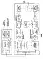
- FIG. 1is a schematic block diagram illustrating a communication system 10 that includes a plurality of base stations and/or access points 12 - 16 , a plurality of wireless communication devices 18 - 32 and a network hardware component 34 .
- the wireless communication devices 18 - 32may be laptop host computers 18 and 26 , personal digital assistant hosts 20 and 30 , personal computer hosts 24 and 32 and/or cellular telephone hosts 22 and 28 .
- the details of the wireless communication deviceswill be described in greater detail with reference to FIG. 2 .
- the base stations or access points 12 - 16are operably coupled to the network hardware 34 via local area network connections 36 , 38 and 40 .
- the network hardware 34which may be a router, switch, bridge, modem, system controller, et cetera provides a wide area network connection 42 for the communication system 10 .
- Each of the base stations or access points 12 - 16has an associated antenna or antenna array to communicate with the wireless communication devices in its area.
- the wireless communication devicesregister with a particular base station or access point 12 - 14 to receive services from the communication system 10 .
- each wireless communication deviceincludes a built-in radio and/or is coupled to a radio.
- the radioincludes a highly linear amplifier and/or programmable multi-stage amplifier as disclosed herein to enhance performance, reduce costs, reduce size, and/or enhance broadband applications.
- FIG. 2is a schematic block diagram illustrating a wireless communication device that includes the host device 18 - 32 and an associated radio 60 .
- the radio 60is a built-in component.
- the radio 60may be built-in or an externally coupled component.
- the host device 18 - 32includes a processing module 50 , memory 52 , radio interface 54 , input interface 58 and output interface 56 .
- the processing module 50 and memory 52execute the corresponding instructions that are typically done by the host device. For example, for a cellular telephone host device, the processing module 50 performs the corresponding communication functions in accordance with a particular cellular telephone standard.
- the radio interface 54allows data to be received from and sent to the radio 60 .
- the radio interface 54For data received from the radio 60 (e.g., inbound data), the radio interface 54 provides the data to the processing module 50 for further processing and/or routing to the output interface 56 .
- the output interface 56provides connectivity to an output display device such as a display, monitor, speakers, et cetera such that the received data may be displayed.
- the radio interface 54also provides data from the processing module 50 to the radio 60 .
- the processing module 50may receive the outbound data from an input device such as a keyboard, keypad, microphone, et cetera via the input interface 58 or generate the data itself.
- the processing module 50may perform a corresponding host function on the data and/or route it to the radio 60 via the radio interface 54 .
- Radio 60includes a host interface 62 , digital receiver processing module 64 , an analog-to-digital converter 66 , a filtering/gain module 68 , an IF mixing down conversion stage 70 , a low noise amplifier 72 , a tuned transformer balun circuit 87 , a local oscillation module 74 , memory 75 , a digital transmitter processing module 76 , a digital-to-analog converter 78 , a filtering/gain module 80 , an IF mixing up conversion stage 82 , a power amplifier 84 , a second tuned transformer balun circuit 89 , and an antenna 86 .
- the antenna 86is shared by the transmit and receive paths via the T/R switch 85 .
- the LNA 72 , balun circuit 87 , T/R switch 85 , balun circuit 89 , and PA 84comprise a front-end of the radio transceiver.
- the digital receiver processing module 64 and the digital transmitter processing module 76in combination with operational instructions stored in memory 75 , execute digital receiver functions and digital transmitter functions, respectively.
- the digital receiver functionsinclude, but are not limited to, digital intermediate frequency to baseband conversion, demodulation, constellation demapping, decoding, and/or descrambling.
- the digital transmitter functionsinclude, but are not limited to, scrambling, encoding, constellation mapping, modulation, and/or digital baseband to IF conversion.
- the digital receiver and transmitter processing modules 64 and 76may be implemented using a shared processing device, individual processing devices, or a plurality of processing devices.
- Such a processing devicemay be a microprocessor, micro-controller, digital signal processor, microcomputer, central processing unit, field programmable gate array, programmable logic device, state machine, logic circuitry, analog circuitry, digital circuitry, and/or any device that manipulates signals (analog and/or digital) based on operational instructions.
- the memory 75may be a single memory device or a plurality of memory devices.
- Such a memory devicemay be a read-only memory, random access memory, volatile memory, non-volatile memory, static memory, dynamic memory, flash memory, and/or any device that stores digital information.
- the processing module 64 and/or 76implements one or more of its functions via a state machine, analog circuitry, digital circuitry, and/or logic circuitry
- the memory storing the corresponding operational instructionsis embedded with the circuitry comprising the state machine, analog circuitry, digital circuitry, and/or logic circuitry.
- the radio 60receives outbound data 94 from the host device via the host interface 62 .
- the host interface 62routes the outbound data 94 to the digital transmitter processing module 76 , which processes the outbound data 94 in accordance with a particular wireless communication standard (e.g., IEEE 802.11 Bluetooth, et cetera) to produce digital transmission formatted data 96 .
- the digital transmission formatted data 96will be a digital base-band signal or a digital low IF signal, where the low IF typically will be in the frequency range of one hundred kilohertz to a few megahertz.
- the digital-to-analog converter 78converts the digital transmission formatted data 96 from the digital domain to the analog domain.
- the filtering/gain module 80filters and/or adjusts the gain of the analog signal prior to providing it to the IF mixing stage 82 .
- the IF mixing stage 82converts the analog baseband or low IF signal into an RF signal based on a transmitter local oscillation 83 provided by local oscillation module 74 .
- the power amplifier 84amplifies the RF signal to produce outbound RF signal 98 , which is provide to the antenna 86 via the tuned transformer balun circuit 89 , where the antenna 86 transmits the outbound RF signal 98 to a targeted device such as a base station, an access point and/or another wireless communication device. Note that the tuned transformer balun circuit 89 will be described in greater detail with reference to FIG. 6 .
- the radio 60also receives an inbound RF signal 88 via the antenna 86 , which was transmitted by a base station, an access point, or another wireless communication device.
- the antenna 86provides the inbound RF signal 88 to the low noise amplifier 72 via the tuned transformer balun circuit 87 , which will be described in greater detail with reference to FIGS. 3-5 .
- the low noise amplifier 72amplifies the signal 88 to produce an amplified inbound RF signal.
- the low noise amplifier 72provides the amplified inbound RF signal to the IF mixing module 70 , which directly converts the amplified inbound RF signal into an inbound low IF signal or baseband signal based on a receiver local oscillation 81 provided by local oscillation module 74 .
- the down conversion module 70provides the inbound low IF signal or baseband signal to the filtering/gain module 68 .
- the filtering/gain module 68filters and/or gains the inbound low IF signal or the inbound baseband signal to produce a filtered inbound signal.
- the analog-to-digital converter 66converts the filtered inbound signal from the analog domain to the digital domain to produce digital reception formatted data 90 .
- the digital receiver processing module 64decodes, descrambles, demaps, and/or demodulates the digital reception formatted data 90 to recapture inbound data 92 in accordance with the particular wireless communication standard being implemented by radio 60 .
- the host interface 62provides the recaptured inbound data 92 to the host device 18 - 32 via the radio interface 54 .
- the wireless communication device of FIG. 2may be implemented using one or more integrated circuits.
- the host devicemay be implemented on one integrated circuit
- the digital receiver processing module 64the digital transmitter processing module 76 and memory 75 may be implemented on a second integrated circuit
- the remaining components of the radio 60less the antenna 86
- the radio 60may be implemented on a single integrated circuit.
- the processing module 50 of the host device and the digital receiver and transmitter processing modules 64 and 76may be a common processing device implemented on a single integrated circuit.
- the memory 52 and memory 75may be implemented on a single integrated circuit and/or on the same integrated circuit as the common processing modules of processing module 50 and the digital receiver and transmitter processing module 64 and 76 .
- FIG. 3is a schematic block diagram of the transformer balun circuit 87 that includes a balun 97 and compensation circuitry 91 .
- the compensation circuitry 91includes ground compensation circuitry 100 and two adjustable capacitors C 1 and C 2 .
- the balun 97includes a single ended winding coupled to the T/R switch 85 and a differential winding coupled to the LNA 72 .
- the differential windingincludes a center tap that is coupled to the circuit ground connection of the LNA 72 , which helps to reduce amplitude imbalances.
- the input and/or output impedance of the balun circuit 87is determined. If the measured impedance is not at a desired level (e.g., 50 Ohms for the input impedance), one or more of capacitors C 1 and C 2 are adjusted to change the impedance such that impedance imbalances are reduced.
- a desired levele.g. 50 Ohms for the input impedance
- the ground compensation circuitry 100reduces phase imbalances of the balun circuit 87 .
- the balun 97may have a turns ratio of 7 to 2 with inductance values ranging from a few tenths of a nano-Henry to tens of nano-Henries.
- the capacitance values of capacitors C 1 and C 2may range from a few tenths of a pico-Farad to hundreds of pico-Farads depending on the frequency range of operation of the radio 60 .
- FIG. 4is a schematic block diagram of an embodiment of the ground compensation circuitry 100 .
- the ground compensation circuitry 100includes an on-chip capacitor, a die pad, and a bond wire coupled to a circuit ground.
- the capacitance value of the on-chip capacitoris selected to resonate with the inductance of the bond wire at operating frequencies of the radio 60 .
- a low impedance groundis provided at the operating frequencies thereby reducing phase imbalances of the balun circuit 87 .
- FIG. 5is a schematic block diagram of another embodiment of the ground compensation circuitry 100 .
- the ground compensation circuitry 100includes a die pad, a bond wire, and an off-chip capacitor coupled to a circuit ground.
- the capacitance value of the off-chip capacitoris selected to resonate with the inductance of the bond wire at operating frequencies of the radio 60 .
- a low impedance groundis provided at the operating frequencies thereby reducing phase imbalances of the balun circuit 87 .
- FIG. 6is a schematic block diagram of a tuned transformer balun circuit 89 that includes a transformer balun 99 , a 1 st capacitor C 5 , a 2 nd capacitor C 3 , and a 3 rd capacitor C 4 .
- the transformer balun 99includes a single-ended winding and a differential winding.
- the single-ended windingis coupled to the T/R switch via capacitor C 5 .
- the differential windingis coupled to the power amplifier 84 .
- the antenna 86via the T/R switch, and the power amplifier 84 provide a load on the transformer balun 99 .
- capacitor C 3 , C 4 and C 5are tuned to resonant with the inductance of the transformer balun 99 taking into account the loading provided by antenna 86 and the power amplifier 84 .
- the inductance of the transformermay be in the neighborhood of a few tenths of nano-henries to nano-henries and the capacitance value of each capacitor C 3 , C 4 and C 5 may be in the range of tens of femto-farads to pico-farads.
- the impedance on the single-ended winding via capacitor C 5may substantially match the impedance on the differential side thereby enabling more efficient energy transfer when the radio is in the transmit mode.
- the term “substantially” or “approximately”, as may be used herein,provides an industry-accepted tolerance to its corresponding term and/or relativity between items. Such an industry-accepted tolerance ranges from less than one percent to twenty percent and corresponds to, but is not limited to, component values, integrated circuit process variations, temperature variations, rise and fall times, and/or thermal noise. Such relativity between items ranges from a difference of a few percent to magnitude differences.
- operably coupledincludes direct coupling and indirect coupling via another component, element, circuit, or module where, for indirect coupling, the intervening component, element, circuit, or module does not modify the information of a signal but may adjust its current level, voltage level, and/or power level.
- inferred couplingi.e., where one element is coupled to another element by inference
- inferred couplingincludes direct and indirect coupling between two elements in the same manner as “operably coupled”.
- the term “compares favorably”, as may be used herein,indicates that a comparison between two or more elements, items, signals, etc., provides a desired relationship. For example, when the desired relationship is that signal 1 has a greater magnitude than signal 2 , a favorable comparison may be achieved when the magnitude of signal 1 is greater than that of signal 2 or when the magnitude of signal 2 is less than that of signal 1 .
Landscapes
- Engineering & Computer Science (AREA)
- Computer Networks & Wireless Communication (AREA)
- Signal Processing (AREA)
- Transceivers (AREA)
Abstract
Description
Claims (11)
Priority Applications (1)
| Application Number | Priority Date | Filing Date | Title |
|---|---|---|---|
| US10/852,470US7269391B2 (en) | 2004-03-16 | 2004-05-24 | Tunable transceiver front end |
Applications Claiming Priority (2)
| Application Number | Priority Date | Filing Date | Title |
|---|---|---|---|
| US10/802,015US7129803B2 (en) | 2004-03-16 | 2004-03-16 | Tuned transformer balun circuit and applications thereof |
| US10/852,470US7269391B2 (en) | 2004-03-16 | 2004-05-24 | Tunable transceiver front end |
Related Parent Applications (1)
| Application Number | Title | Priority Date | Filing Date |
|---|---|---|---|
| US10/802,015Continuation-In-PartUS7129803B2 (en) | 2004-03-16 | 2004-03-16 | Tuned transformer balun circuit and applications thereof |
Publications (2)
| Publication Number | Publication Date |
|---|---|
| US20050208901A1 US20050208901A1 (en) | 2005-09-22 |
| US7269391B2true US7269391B2 (en) | 2007-09-11 |
Family
ID=46302098
Family Applications (1)
| Application Number | Title | Priority Date | Filing Date |
|---|---|---|---|
| US10/852,470Expired - Fee RelatedUS7269391B2 (en) | 2004-03-16 | 2004-05-24 | Tunable transceiver front end |
Country Status (1)
| Country | Link |
|---|---|
| US (1) | US7269391B2 (en) |
Cited By (16)
| Publication number | Priority date | Publication date | Assignee | Title |
|---|---|---|---|---|
| US20070279099A1 (en)* | 2006-05-30 | 2007-12-06 | Jennic Limited | Transceiver and method of operating an electrical circuit |
| US20080139158A1 (en)* | 2006-12-06 | 2008-06-12 | Yuyu Chang | Method and system for a transformer-based high performance cross-coupled low noise amplifier |
| US20090036065A1 (en)* | 2007-08-01 | 2009-02-05 | Crystalmedia Technology, Inc. | Transmit/receive switch |
| US20090039977A1 (en)* | 2007-08-07 | 2009-02-12 | Samsung Electro-Mechanics Co., Ltd. | Balun transformer |
| US20090143033A1 (en)* | 2007-11-29 | 2009-06-04 | Broadcom Corporation | Gain control using a dynamically configurable transformer |
| US20090289721A1 (en)* | 2008-05-09 | 2009-11-26 | Texas Instruments Incorporated | Circuits, processes, devices and systems for full integration of rf front end module including rf power amplifier |
| US20090323859A1 (en)* | 2008-06-26 | 2009-12-31 | Bishop James W | Flexible, Reconfigurable, Power Efficient Transmitter and Method |
| US20100167667A1 (en)* | 2008-12-30 | 2010-07-01 | Stmicroelectronics (Tours) Sas | Setting of a balun |
| US20100248660A1 (en)* | 2009-03-24 | 2010-09-30 | Bavisi Amit D | RF Multiband Transmitter with Balun |
| US8135357B1 (en)* | 2005-12-13 | 2012-03-13 | Qualcomm Atheros, Inc. | Integrated transmitter/receiver switch with impedance matching network |
| US20120068782A1 (en)* | 2008-03-27 | 2012-03-22 | Ahmadreza Rofougaran | Method and System for Configurable Differential or Single-Ended Signaling in an Integrated Circuit |
| US8436695B2 (en) | 2010-12-01 | 2013-05-07 | Telefonaktiebolaget Lm Ericsson (Publ) | Imbalance detection and reduction for wideband balun |
| US20130328736A1 (en)* | 2012-06-11 | 2013-12-12 | Melexis Technologies N.V. | Adaptation of an antenna circuit for a near-field communication terminal |
| US20160226553A1 (en)* | 2014-12-30 | 2016-08-04 | Skyworks Solutions, Inc. | Integrated cmos transmit/receive switch in a radio frequency device |
| US10181828B2 (en) | 2016-06-29 | 2019-01-15 | Skyworks Solutions, Inc. | Active cross-band isolation for a transformer-based power amplifier |
| US12184311B2 (en) | 2021-03-25 | 2024-12-31 | Skyworks Solutions, Inc. | Antenna systems with both single-ended and differential signal feeds |
Families Citing this family (20)
| Publication number | Priority date | Publication date | Assignee | Title |
|---|---|---|---|---|
| US20070135064A1 (en)* | 2005-12-09 | 2007-06-14 | Ruelke Charles R | Method and apparatus for reducing phase imbalance in radio frequency signals |
| US7899409B2 (en)* | 2006-01-30 | 2011-03-01 | Broadcom Corporation | Apparatus for controlling impedance |
| US20090045885A1 (en)* | 2007-08-17 | 2009-02-19 | Broadcom Corporation | Passive structure for high power and low loss applications |
| US8301186B2 (en)* | 2008-04-04 | 2012-10-30 | Stmicroelectronics Ltd. | Enhanced sensitivity radio frequency front end circuit |
| US20090253384A1 (en)* | 2008-04-04 | 2009-10-08 | Stmicroelectronics, Ltd. | Dual Mode Radio Frequency Front End Circuit |
| US8090327B2 (en)* | 2008-12-02 | 2012-01-03 | Broadcom Corporation | Configurable baseband processing for receiver and transmitter and methods for use therewith |
| GB2491232B (en)* | 2009-10-23 | 2013-01-16 | Cambridge Silicon Radio Ltd | Loop-through circuit |
| US20130127010A1 (en)* | 2010-06-09 | 2013-05-23 | Dsp Group Ltd. | Integrated circuit including a differential power amplifier with a single ended output and an integrated balun |
| US9379753B2 (en)* | 2014-09-15 | 2016-06-28 | Qualcomm Incorporated | On-chip linearity calibration |
| CN105871408B (en)* | 2016-03-31 | 2019-02-26 | 青岛海信电器股份有限公司 | A kind of method of front-end circuit and the signal transmission of radio frequency chip |
| US9793942B1 (en)* | 2016-06-20 | 2017-10-17 | Ubilite, Inc. | Systems and methods for a switchless radio front end |
| US10574286B2 (en)* | 2017-09-01 | 2020-02-25 | Qualcomm Incorporated | High selectivity TDD RF front end |
| EP3471140B1 (en)* | 2017-10-11 | 2022-05-18 | Nxp B.V. | Integrated circuit including a plurality of components including a transformer |
| US10476533B1 (en)* | 2018-04-27 | 2019-11-12 | Speedlink Technology Inc. | Transmit and receive switch and broadband power amplifier matching network for multi-band millimeter-wave 5G communication |
| US11456717B2 (en)* | 2019-10-03 | 2022-09-27 | Texas Instruments Incorporated | Input drive configuration for reducing phase and gain imbalance |
| US11336321B1 (en)* | 2020-11-09 | 2022-05-17 | Stmicroelectronics Sa | Transmitter / receiver device |
| US12199585B2 (en)* | 2020-12-10 | 2025-01-14 | Skyworks Solutions, Inc. | Baluns with integrated matching networks |
| US12095514B2 (en)* | 2021-01-29 | 2024-09-17 | Samsung Electronics Co., Ltd. | Electronic apparatus including antenna and audio interface |
| CN215912076U (en)* | 2021-08-19 | 2022-02-25 | 深圳飞骧科技股份有限公司 | Harmonic suppression matching circuit structure and power amplifier suitable for balun |
| CN116827362B (en)* | 2023-08-29 | 2023-12-22 | 上海移芯通信科技股份有限公司 | Radio frequency circuit, chip, multi-band receiving device and band switching method |
Citations (14)
| Publication number | Priority date | Publication date | Assignee | Title |
|---|---|---|---|---|
| US5644272A (en)* | 1996-03-05 | 1997-07-01 | Telefonaktiebolaget Lm Ericsson | High frequency balun provided in a multilayer substrate |
| US6009318A (en)* | 1997-07-23 | 1999-12-28 | Ericsson Inc. | Electronically adjustable balanced-to-unbalanced converters (balun) |
| US6009314A (en)* | 1997-11-17 | 1999-12-28 | Telefonaktiebolaget L/M Ericsson | Monolithic high frequency antenna switch |
| US6315502B1 (en)* | 1999-01-26 | 2001-11-13 | Jakob Lach Gmbh & Co. Kg | Cutting tool with means for controlling the formation of chips |
| US6351502B1 (en)* | 2000-01-13 | 2002-02-26 | Atheros Communications, Inc. | RF front-end with multistage stepdown filtering architecture |
| US6654595B1 (en)* | 1998-02-01 | 2003-11-25 | Signia-Idt, Inc. | Radio system including mixer device and switching circuit and method having switching signal feedback control for enhanced dynamic range and performance |
| US6735418B1 (en)* | 1999-05-24 | 2004-05-11 | Intel Corporation | Antenna interface |
| US6809581B2 (en)* | 2002-04-23 | 2004-10-26 | Broadcom Corp. | Integrated circuit low noise amplifier and applications thereof |
| US20040253939A1 (en)* | 2003-06-12 | 2004-12-16 | Castaneda Jesus A. | Integrated circuit radio front-end architecture and applications thereof |
| US20050135026A1 (en)* | 2003-12-19 | 2005-06-23 | Shahla Khorram | High frequency integrated circuit pad configuration including ESD protection circuitry |
| US6919858B2 (en)* | 2003-10-10 | 2005-07-19 | Broadcom, Corp. | RF antenna coupling structure |
| US6982609B1 (en)* | 2002-05-15 | 2006-01-03 | Zeevo | System method and apparatus for a three-line balun with power amplifier bias |
| US7020452B1 (en)* | 2003-04-29 | 2006-03-28 | Sirenza Microdevices, Inc. | Actively matched center-tapped marchand balanced mixer |
| US7129803B2 (en)* | 2004-03-16 | 2006-10-31 | Broadcom Corporation | Tuned transformer balun circuit and applications thereof |
- 2004
- 2004-05-24USUS10/852,470patent/US7269391B2/ennot_activeExpired - Fee Related
Patent Citations (15)
| Publication number | Priority date | Publication date | Assignee | Title |
|---|---|---|---|---|
| US5644272A (en)* | 1996-03-05 | 1997-07-01 | Telefonaktiebolaget Lm Ericsson | High frequency balun provided in a multilayer substrate |
| US6009318A (en)* | 1997-07-23 | 1999-12-28 | Ericsson Inc. | Electronically adjustable balanced-to-unbalanced converters (balun) |
| US6009314A (en)* | 1997-11-17 | 1999-12-28 | Telefonaktiebolaget L/M Ericsson | Monolithic high frequency antenna switch |
| US6654595B1 (en)* | 1998-02-01 | 2003-11-25 | Signia-Idt, Inc. | Radio system including mixer device and switching circuit and method having switching signal feedback control for enhanced dynamic range and performance |
| US6315502B1 (en)* | 1999-01-26 | 2001-11-13 | Jakob Lach Gmbh & Co. Kg | Cutting tool with means for controlling the formation of chips |
| US6735418B1 (en)* | 1999-05-24 | 2004-05-11 | Intel Corporation | Antenna interface |
| US6351502B1 (en)* | 2000-01-13 | 2002-02-26 | Atheros Communications, Inc. | RF front-end with multistage stepdown filtering architecture |
| US6809581B2 (en)* | 2002-04-23 | 2004-10-26 | Broadcom Corp. | Integrated circuit low noise amplifier and applications thereof |
| US6982609B1 (en)* | 2002-05-15 | 2006-01-03 | Zeevo | System method and apparatus for a three-line balun with power amplifier bias |
| US7020452B1 (en)* | 2003-04-29 | 2006-03-28 | Sirenza Microdevices, Inc. | Actively matched center-tapped marchand balanced mixer |
| US20040253939A1 (en)* | 2003-06-12 | 2004-12-16 | Castaneda Jesus A. | Integrated circuit radio front-end architecture and applications thereof |
| US6919858B2 (en)* | 2003-10-10 | 2005-07-19 | Broadcom, Corp. | RF antenna coupling structure |
| US20050215205A1 (en)* | 2003-10-10 | 2005-09-29 | Ahmadreza Rofougaran | RF diversity antenna coupling structure |
| US20050135026A1 (en)* | 2003-12-19 | 2005-06-23 | Shahla Khorram | High frequency integrated circuit pad configuration including ESD protection circuitry |
| US7129803B2 (en)* | 2004-03-16 | 2006-10-31 | Broadcom Corporation | Tuned transformer balun circuit and applications thereof |
Cited By (34)
| Publication number | Priority date | Publication date | Assignee | Title |
|---|---|---|---|---|
| US8135357B1 (en)* | 2005-12-13 | 2012-03-13 | Qualcomm Atheros, Inc. | Integrated transmitter/receiver switch with impedance matching network |
| US20070279099A1 (en)* | 2006-05-30 | 2007-12-06 | Jennic Limited | Transceiver and method of operating an electrical circuit |
| US7787830B2 (en)* | 2006-05-30 | 2010-08-31 | Jennic Limited | Transceiver and method of operating an electrical circuit |
| US20080139158A1 (en)* | 2006-12-06 | 2008-06-12 | Yuyu Chang | Method and system for a transformer-based high performance cross-coupled low noise amplifier |
| US8073417B2 (en)* | 2006-12-06 | 2011-12-06 | Broadcom Corporation | Method and system for a transformer-based high performance cross-coupled low noise amplifier |
| US20090036065A1 (en)* | 2007-08-01 | 2009-02-05 | Crystalmedia Technology, Inc. | Transmit/receive switch |
| US7702296B2 (en)* | 2007-08-01 | 2010-04-20 | Mediatek Usa Inc. | Transmit/receive switch |
| US7777589B2 (en)* | 2007-08-07 | 2010-08-17 | Samsung Electro-Mechanics Co., Ltd. | Balun transformer |
| US20090039977A1 (en)* | 2007-08-07 | 2009-02-12 | Samsung Electro-Mechanics Co., Ltd. | Balun transformer |
| US8862077B2 (en) | 2007-11-29 | 2014-10-14 | Broadcom Corporation | Gain control using a dynamically configurable transformer |
| US8515368B2 (en)* | 2007-11-29 | 2013-08-20 | Broadcom Corporation | Gain control using a dynamically configurable transformer |
| US20090143033A1 (en)* | 2007-11-29 | 2009-06-04 | Broadcom Corporation | Gain control using a dynamically configurable transformer |
| US8319578B2 (en)* | 2008-03-27 | 2012-11-27 | Broadcom Corporation | Method and system for configurable differential or single-ended signaling in an integrated circuit |
| US20120068782A1 (en)* | 2008-03-27 | 2012-03-22 | Ahmadreza Rofougaran | Method and System for Configurable Differential or Single-Ended Signaling in an Integrated Circuit |
| US8483627B2 (en) | 2008-05-09 | 2013-07-09 | Texas Instruments Incorporated | Circuits, processes, devices and systems for full integration of RF front end module including RF power amplifier |
| US20090289721A1 (en)* | 2008-05-09 | 2009-11-26 | Texas Instruments Incorporated | Circuits, processes, devices and systems for full integration of rf front end module including rf power amplifier |
| US20090323859A1 (en)* | 2008-06-26 | 2009-12-31 | Bishop James W | Flexible, Reconfigurable, Power Efficient Transmitter and Method |
| US8299869B2 (en)* | 2008-12-30 | 2012-10-30 | Stmicroelectronics (Tours) Sas | Setting of a balun |
| US20100167667A1 (en)* | 2008-12-30 | 2010-07-01 | Stmicroelectronics (Tours) Sas | Setting of a balun |
| US8068795B2 (en) | 2009-03-24 | 2011-11-29 | Freescale Semiconductor, Inc. | RF multiband transmitter with balun |
| US20100248660A1 (en)* | 2009-03-24 | 2010-09-30 | Bavisi Amit D | RF Multiband Transmitter with Balun |
| US8436695B2 (en) | 2010-12-01 | 2013-05-07 | Telefonaktiebolaget Lm Ericsson (Publ) | Imbalance detection and reduction for wideband balun |
| US8884715B2 (en) | 2010-12-01 | 2014-11-11 | Telefonaktiebolaget Lm Ericsson (Publ) | Imbalance detection and reduction for wideband balun |
| US20130328736A1 (en)* | 2012-06-11 | 2013-12-12 | Melexis Technologies N.V. | Adaptation of an antenna circuit for a near-field communication terminal |
| US10249946B2 (en)* | 2012-06-11 | 2019-04-02 | Stmicroelectronics (Rousset) Sas | Adaptation of an antenna circuit for a near-field communication terminal |
| US10135405B2 (en) | 2014-12-30 | 2018-11-20 | Skyworks Solutions, Inc. | Dynamic tuning of a transformer-based radio frequency power amplifier |
| US10103695B2 (en)* | 2014-12-30 | 2018-10-16 | Skyworks Solutions, Inc. | Integrated CMOS transmit/receive switch in a radio frequency device |
| US10148233B2 (en) | 2014-12-30 | 2018-12-04 | Skyworks Solutions, Inc. | Transmit-receive isolation in a transformer-based radio frequency power amplifier |
| US20160226553A1 (en)* | 2014-12-30 | 2016-08-04 | Skyworks Solutions, Inc. | Integrated cmos transmit/receive switch in a radio frequency device |
| US20190158043A1 (en)* | 2014-12-30 | 2019-05-23 | Skyworks Solutions, Inc. | Integrated cmos transmit/receive switch in a radio frequency device |
| US10581388B2 (en)* | 2014-12-30 | 2020-03-03 | Skyworks Solutions, Inc. | Integrated CMOS transmit/receive switch in a radio frequency device |
| US10181828B2 (en) | 2016-06-29 | 2019-01-15 | Skyworks Solutions, Inc. | Active cross-band isolation for a transformer-based power amplifier |
| US10547278B2 (en) | 2016-06-29 | 2020-01-28 | Skyworks Solutions, Inc. | Active cross-band isolation for a transformer-based power amplifier |
| US12184311B2 (en) | 2021-03-25 | 2024-12-31 | Skyworks Solutions, Inc. | Antenna systems with both single-ended and differential signal feeds |
Also Published As
| Publication number | Publication date |
|---|---|
| US20050208901A1 (en) | 2005-09-22 |
Similar Documents
| Publication | Publication Date | Title |
|---|---|---|
| US7269391B2 (en) | Tunable transceiver front end | |
| US8380153B2 (en) | Radio front end and applications thereof | |
| US7129803B2 (en) | Tuned transformer balun circuit and applications thereof | |
| US7170465B2 (en) | RF diversity antenna coupling structure | |
| US7796970B2 (en) | Integrated low noise amplifier | |
| US6882228B2 (en) | Radio frequency integrated circuit having an antenna diversity structure | |
| US7245887B2 (en) | High speed CMOS transmit-receive antenna switch | |
| US7369096B2 (en) | Impedance matched passive radio frequency transmit/receive switch | |
| US7551901B2 (en) | Linear high powered integrated circuit amplifier | |
| US7974599B2 (en) | Low noise amplifier with constant input impedance | |
| US7079816B2 (en) | On chip diversity antenna switch | |
| US7092679B2 (en) | Low loss diversity antenna T/R switch | |
| US6907231B2 (en) | On-chip impedance matching power amplifier and radio applications thereof | |
| US7391596B2 (en) | High frequency integrated circuit pad configuration including ESD protection circuitry | |
| US7184735B2 (en) | Radio frequency integrated circuit having symmetrical differential layout | |
| US20060066431A1 (en) | Adjustable differential inductor | |
| US7457380B2 (en) | Low noise circuit and applications thereof |
Legal Events
| Date | Code | Title | Description |
|---|---|---|---|
| AS | Assignment | Owner name:BROADCOM CORPORATION, CALIFORNIA Free format text:ASSIGNMENT OF ASSIGNORS INTEREST;ASSIGNORS:CHIU, JANICE;KHORRAM, SHAHLA;LI, QIANG (TOM);REEL/FRAME:015382/0233 Effective date:20040518 | |
| FEPP | Fee payment procedure | Free format text:PAYOR NUMBER ASSIGNED (ORIGINAL EVENT CODE: ASPN); ENTITY STATUS OF PATENT OWNER: LARGE ENTITY | |
| STCF | Information on status: patent grant | Free format text:PATENTED CASE | |
| FPAY | Fee payment | Year of fee payment:4 | |
| FPAY | Fee payment | Year of fee payment:8 | |
| AS | Assignment | Owner name:BANK OF AMERICA, N.A., AS COLLATERAL AGENT, NORTH CAROLINA Free format text:PATENT SECURITY AGREEMENT;ASSIGNOR:BROADCOM CORPORATION;REEL/FRAME:037806/0001 Effective date:20160201 Owner name:BANK OF AMERICA, N.A., AS COLLATERAL AGENT, NORTH Free format text:PATENT SECURITY AGREEMENT;ASSIGNOR:BROADCOM CORPORATION;REEL/FRAME:037806/0001 Effective date:20160201 | |
| AS | Assignment | Owner name:AVAGO TECHNOLOGIES GENERAL IP (SINGAPORE) PTE. LTD., SINGAPORE Free format text:ASSIGNMENT OF ASSIGNORS INTEREST;ASSIGNOR:BROADCOM CORPORATION;REEL/FRAME:041706/0001 Effective date:20170120 Owner name:AVAGO TECHNOLOGIES GENERAL IP (SINGAPORE) PTE. LTD Free format text:ASSIGNMENT OF ASSIGNORS INTEREST;ASSIGNOR:BROADCOM CORPORATION;REEL/FRAME:041706/0001 Effective date:20170120 | |
| AS | Assignment | Owner name:BROADCOM CORPORATION, CALIFORNIA Free format text:TERMINATION AND RELEASE OF SECURITY INTEREST IN PATENTS;ASSIGNOR:BANK OF AMERICA, N.A., AS COLLATERAL AGENT;REEL/FRAME:041712/0001 Effective date:20170119 | |
| AS | Assignment | Owner name:AVAGO TECHNOLOGIES INTERNATIONAL SALES PTE. LIMITE Free format text:MERGER;ASSIGNOR:AVAGO TECHNOLOGIES GENERAL IP (SINGAPORE) PTE. LTD.;REEL/FRAME:047196/0097 Effective date:20180509 | |
| AS | Assignment | Owner name:AVAGO TECHNOLOGIES INTERNATIONAL SALES PTE. LIMITE Free format text:CORRECTIVE ASSIGNMENT TO CORRECT THE EXECUTION DATE PREVIOUSLY RECORDED AT REEL: 047196 FRAME: 0097. ASSIGNOR(S) HEREBY CONFIRMS THE MERGER;ASSIGNOR:AVAGO TECHNOLOGIES GENERAL IP (SINGAPORE) PTE. LTD.;REEL/FRAME:048555/0510 Effective date:20180905 | |
| FEPP | Fee payment procedure | Free format text:MAINTENANCE FEE REMINDER MAILED (ORIGINAL EVENT CODE: REM.); ENTITY STATUS OF PATENT OWNER: LARGE ENTITY | |
| LAPS | Lapse for failure to pay maintenance fees | Free format text:PATENT EXPIRED FOR FAILURE TO PAY MAINTENANCE FEES (ORIGINAL EVENT CODE: EXP.); ENTITY STATUS OF PATENT OWNER: LARGE ENTITY | |
| STCH | Information on status: patent discontinuation | Free format text:PATENT EXPIRED DUE TO NONPAYMENT OF MAINTENANCE FEES UNDER 37 CFR 1.362 | |
| FP | Lapsed due to failure to pay maintenance fee | Effective date:20190911 |