US7269212B1 - Low-latency equalization in multi-level, multi-line communication systems - Google Patents
Low-latency equalization in multi-level, multi-line communication systemsDownload PDFInfo
- Publication number
- US7269212B1 US7269212B1US09/654,643US65464300AUS7269212B1US 7269212 B1US7269212 B1US 7269212B1US 65464300 AUS65464300 AUS 65464300AUS 7269212 B1US7269212 B1US 7269212B1
- Authority
- US
- United States
- Prior art keywords
- signal
- driver
- equalization
- input signals
- output
- Prior art date
- Legal status (The legal status is an assumption and is not a legal conclusion. Google has not performed a legal analysis and makes no representation as to the accuracy of the status listed.)
- Expired - Lifetime, expires
Links
Images


Classifications
- H—ELECTRICITY
- H04—ELECTRIC COMMUNICATION TECHNIQUE
- H04L—TRANSMISSION OF DIGITAL INFORMATION, e.g. TELEGRAPHIC COMMUNICATION
- H04L25/00—Baseband systems
- H04L25/02—Details ; arrangements for supplying electrical power along data transmission lines
- H04L25/03—Shaping networks in transmitter or receiver, e.g. adaptive shaping networks
- H04L25/03878—Line equalisers; line build-out devices
- H—ELECTRICITY
- H04—ELECTRIC COMMUNICATION TECHNIQUE
- H04L—TRANSMISSION OF DIGITAL INFORMATION, e.g. TELEGRAPHIC COMMUNICATION
- H04L25/00—Baseband systems
- H04L25/02—Details ; arrangements for supplying electrical power along data transmission lines
- H04L25/03—Shaping networks in transmitter or receiver, e.g. adaptive shaping networks
- H04L25/03006—Arrangements for removing intersymbol interference
- H04L2025/0335—Arrangements for removing intersymbol interference characterised by the type of transmission
- H04L2025/03356—Baseband transmission
- H04L2025/03363—Multilevel
- H—ELECTRICITY
- H04—ELECTRIC COMMUNICATION TECHNIQUE
- H04L—TRANSMISSION OF DIGITAL INFORMATION, e.g. TELEGRAPHIC COMMUNICATION
- H04L25/00—Baseband systems
- H04L25/02—Details ; arrangements for supplying electrical power along data transmission lines
- H04L25/03—Shaping networks in transmitter or receiver, e.g. adaptive shaping networks
- H04L25/03006—Arrangements for removing intersymbol interference
- H04L2025/03433—Arrangements for removing intersymbol interference characterised by equaliser structure
- H04L2025/03439—Fixed structures
- H04L2025/03445—Time domain
- H04L2025/03471—Tapped delay lines
- H04L2025/03477—Tapped delay lines not time-recursive
- H—ELECTRICITY
- H04—ELECTRIC COMMUNICATION TECHNIQUE
- H04L—TRANSMISSION OF DIGITAL INFORMATION, e.g. TELEGRAPHIC COMMUNICATION
- H04L25/00—Baseband systems
- H04L25/02—Details ; arrangements for supplying electrical power along data transmission lines
- H04L25/0264—Arrangements for coupling to transmission lines
- H04L25/028—Arrangements specific to the transmitter end
- H—ELECTRICITY
- H04—ELECTRIC COMMUNICATION TECHNIQUE
- H04L—TRANSMISSION OF DIGITAL INFORMATION, e.g. TELEGRAPHIC COMMUNICATION
- H04L25/00—Baseband systems
- H04L25/02—Details ; arrangements for supplying electrical power along data transmission lines
- H04L25/03—Shaping networks in transmitter or receiver, e.g. adaptive shaping networks
- H04L25/03006—Arrangements for removing intersymbol interference
- H04L25/03343—Arrangements at the transmitter end
Definitions
- the present inventionrelates to multi-level digital signaling, and in particular to techniques to equalize or compensate for errors that may otherwise be present in a multi-level, multi-line signaling system.
- multi-level signalingis sometimes known as multiple pulse amplitude modulation or multi-PAM, and has been implemented with radio or other long-distance wireless signaling systems.
- Equalization techniques for long-distance multi-level signaling systemssuch as those used in radio or telecommunication networks commonly include adaptive filters, which can change equalization characteristics adaptively to improve equalization accuracy or in response to changing conditions. The complexities of these equalization techniques can delay signaling by slight but tolerable amounts for these long-distance systems.
- Multi-PAMis not traditionally used for communication between devices in close proximity or belonging to the same system, such as those connected to the same integrated circuit (IC) or printed circuit board (PCB).
- ICintegrated circuit
- PCBprinted circuit board
- One reason for thismay be that within such a system the characteristics of transmission lines, such as buses or signal lines, over which signals travel are tightly controlled, so that increases in data rate may be achieved by simply increasing data frequency.
- receiving devicesmay have a reduced ability to distinguish binary signals, so that dividing signals into smaller levels for multi-PAM is problematic.
- Multi-PAMmay also be more difficult to implement in multi-drop bus systems (i.e., buses shared by multiple processing mechanisms), since the lower signal-to-noise ratio for such systems sometimes results in bit errors even for binary signals.
- complex equalization techniquessuch as employed for long distance communication systems may not be feasible in a bus system for which low latency is a performance criterion.
- the present inventionis directed to low-latency equalization mechanisms for short-range communications systems.
- Such equalization mechanismsmay compensate for signal attenuation along a transmission line, reflections due to impedance discontinuities along such a line, and crosstalk between adjacent lines.
- the equalization mechanismsmay be particularly advantageous for multi-PAM communications systems.
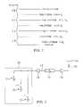
- FIG. 1shows a multi-level signaling system having four logical states corresponding to four voltage ranges.
- FIG. 2shows a representative signaling device that may be used to create the voltage levels of FIG. 1 .
- FIG. 3depicts an issue with a multi-PAM signaling system such as the 4-PAM system shown in FIG. 1 and FIG. 2 .
- FIG. 4shows a solution to the issue depicted in FIG. 3 .
- FIG. 5depicts a multi-level (4-PAM) signaling system in which voltage ranges for the logic states are shifted by varying amounts to implement the solution shown in FIG. 4 .
- FIG. 6provides a table illustrating the signal levels involved in transitioning between the logical states of FIG. 5 .
- FIG. 7Ashows initial, transition and final states of a signal that may represent a transition illustrated in FIG. 6 .
- FIG. 7Bshows initial, transition and final states of a main component of the signal shown in FIG. 7A .
- FIG. 7Cshows initial, transition and final states of an auxiliary component of the signal shown in FIG. 7A .
- FIG. 8shows a device that can provide the transition signals shown in FIG. 6 and FIGS. 7A-C .
- FIG. 9shows a finite impulse response (FIR) filter representation of the device of FIG. 8 .
- FIG. 10shows a general equalization system for a signal line, including a self equalization FIR filter and a number of crosstalk equalization FIRs.
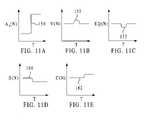
- FIG. 11Ashows a signal transition that may create crosstalk on adjacent signal lines.
- FIG. 11Bshows crosstalk noise from the signal transition of FIG. 11A , imposed on a signal in an adjacent line.
- FIG. 11Cshows an equalization signal that compensates for the crosstalk noise shown in FIG. 11B .
- FIG. 11Dshows a first component of the equalization signal shown in FIG. 11C .
- FIG. 11Eshows a second component of the equalization signal shown in FIG. 11C .
- FIG. 12shows a signal driver, self-equalization and crosstalk equalization communication device.
- FIG. 13shows an equalization mechanism that inputs MSB and LSB signals to provide compensation.
- FIG. 14shows a general FIR filter having a number of self-equalization and crosstalk-equalization mechanisms tapped at various delay times.
- FIG. 15illustrates a mechanism for adjusting equalization parameters such as the magnitude, timing and sign of various equalization signals.
- FIG. 16shows an encoder that converts MSB and LSB signals into input signals for the output driver and equalization mechanisms.
- FIG. 17shows receiver that receives the multi-level signals sent by the main and auxiliary drivers and decode the signals into MSB and LSB components.
- FIG. 18Ashows a signal transition that has a high-frequency noise spike.
- FIG. 18Bshows an equalization signal designed to compensate for a DC component of the spike of FIG. 18 a and FIG. 18 b by integration.
- FIG. 18shows a combination of the signals of FIGS. 18 b - 18 c - and - FIG. 18E shows an integration signal of FIG. 18D
- FIG. 19shows a system with a number of adjacent signal lines that may create crosstalk, and standardized FIR filters coupled between the lines.
- FIG. 20shows a system with a number of adjacent signal lines grouped in pairs with a ground wire disposed between the pairs of lines and standardized FIR filters coupled between the lines.
- FIG. 21illustrates a memory system in which embodiments of the present invention may be applied.
- FIG. 1shows a multi-level signaling system having four logical states corresponding to four voltage levels, VOUT 0 , VOUT 1 , VOUT 2 and VOUT 3 .
- the voltage levels in this exampleare all positive relative to ground, and range as high as VTERM.
- VOUT 0is defined to be above VREFH
- VOUT 1is defined to be between VREFM and VREFH
- VOUT 2is defined to be between VREFL and VREFM
- VOUT 3is defined to be less than VREFL.
- VOUT 0corresponds to logical state 00
- VOUT 1corresponds to logical state 01
- VOUT 2corresponds to logical state 11
- VOUT 3corresponds to logical state 10.
- a first bit of each logical stateis termed the most significant bit (MSB) and a second bit of each logical state is termed the least significant bit (LSB).
- MSBmost significant bit
- LSBleast significant bit
- Each logical statemay be termed a dual-bit, since it provides information regarding two bits. Data may be transmitted and read at both rising and falling edge of a clock cycle, so that each bit signal and each dual-bit signal has a duration of one-half the clock cycle.
- the logical statesare arranged in a Gray coded order, so that an erroneous reading of an adjacent logic state produces an error in only one of the bits. Another characteristic of this logical 4-PAM arrangement is that setting the LSB equal to zero for all states results in a 2-PAM scheme.
- the logical statescan be arranged in binary (00, 01, 10, 11) or other order.
- the communication systemis employed for a memory bus, which may for instance include random access memory (RAM), like that disclosed in U.S. Pat. No. 5,243,703 to Farmwald et al., which is incorporated herein by reference.
- RAMrandom access memory
- the multi-PAM communication and low-latency signal correction techniques disclosed hereinmay also be used for other contained systems, such as for communication between processors of a multiprocessor apparatus, or between a processor and a peripheral device, such as a disk drive controller or network interface card over an input/output bus.
- FIG. 2shows a representation of a communication system that may be used to create the voltage levels of FIG. 1 .
- An output driver 20drives signals to output pad 18 and over transmission line 16 , which may for example be a memory bus or other interconnection between devices affixed to a circuit board, to be received at pad 25 .
- Transmission line 16has a characteristic impedance Z 0 27 that is substantially matched with a terminating resistor 29 to minimize reflections.
- Output driver 20includes first 21 , second 22 and third 23 transistor current sources, which together produce a current I when all are active, pulling the voltage at pad 25 down from VTERM by I ⁇ Z 0 , signaling logical state 10 under the Gray code system.
- VOUT 0VTERM
- current sources 21 , 22 and 23are all turned off.
- VOUT 1VTERM ⁇ (1 ⁇ 3)I ⁇ Z 0
- signaling logical state 01one of the current sources is turned on
- the logical level 00is chosen to have zero current flow to reduce power consumption for the situation in which much of the data transmitted has a MSB and LSB of zero.
- FIG. 3depicts an issue with a multi-PAM signaling system such as the 4-PAM system mentioned above.
- a multi-PAM signaling systemsuch as the 4-PAM system mentioned above.
- different amounts of signal lossmay occur depending upon the magnitude of the transition between logic levels. For instance, transitioning between a 10 state and a 00 state may have a greater signal deficiency than a transition between a 11 state and the 00 state, which in turn has a greater signal deficiency than a transition between 01 state and the 00 state, while maintaining the same logic state over plural bit periods may have no attenuation error.
- each different transition between statesmay have a different associated error. Complicating matters is the transitory nature of the errors as demonstrated, for example, by the fact that maintaining a constant logic state may generate no error, regardless of the previous transition magnitude to that logic state and the error associated with that transition.
- FIG. 4shows the addition of a different equalization signal, 3 S, 2 S or S to the main signal when driving different transitions, the equalization signals compensating for the attenuation of the received signal.
- the equalization signals in this embodimentare transitory, so that each may for instance have a duration less than or equal to one bit signal, after which the equalization signal is terminated, allowing the initially overdriven signal to maintain a steady state logic level.
- the equalization signals S, 2 S or 3 Sadd predetermined high-frequency components to the transition signals that raise the slope of the edge of the transition.
- a difficulty with this approach for a system such as shown in FIG. 1is that the voltage can only be pulled down from VTERM, unless negative current could flow through current sources 21 - 23 . In other words, with the 00 level set at VTERM in FIG. 5 it is difficult for the equalizing S, 2S or 3S to add to the transition above VTERM.
- FIG. 5depicts a multi-level (4-PAM) signaling system in which the 00 logic state is reduced below VTERM by 3S, in order to allow overdriving a transition for example from the 10 to the 00 state by 3S.
- This 00 logic levelis termed A, and can be provided by having none of the main current drivers turned on and three equalization drivers turned on, for a voltage level of 0M+3S.
- the 10 level(termed D) can be pulled lower if necessary to overdrive a transition, and so it is characterized by having three main drivers or current sources turned on, but zero equalization drivers turned on, for a total voltage level of 3M+0S.
- Logical state 01also termed level B, has a voltage of 1M+2S
- state 11, termed level Chas a voltage of 2M+1S.
- the reference levels that provide boundaries between the signal levelsare also shifted in accordance with the shift in the signal levels.
- VRHis defined in this system to be equal to VTERM ⁇ (1 ⁇ 2) [(1 ⁇ 3)+( 5/3) (S/M)]I ⁇ Z 0
- VRMis defined in this system to be equal to VTERM ⁇ (1 ⁇ 2) [1+(S/M)]I ⁇ Z 0
- VRLis defined in this system to be equal to VTERM ⁇ (1 ⁇ 2)[( 5/3)+(1 ⁇ 3) (S/M)]I ⁇ Z 0 .
- FIG. 6provides a table illustrating the drive signal levels involved in transitioning between the logical states of FIG. 5 .
- an overdriven transition drive signal of 3M+3Sis provided in order to transition from initial state A (0M+3S) to final state D (3M+0S).
- an overdriven transition drive signal of 3M+3Sis provided in order to transition from initial state A (0M+3S) to final state D (3M+0S).
- changing from an initial state D (3M+0S) to final state A (0M+3S)involves a drive signal of 0M+0S.
- the transition drive signal in this examplehas an overdriven duration that is equal to that of one bit (or dual-bit) signal, although in general an overdriven period of a drive signal may have a duration that is less than or greater than that of a bit signal.
- a drive signalmay be overdriven for a first portion of a bit signal time, with a second portion of that signal not being overdriven.
- the M multiplieris the complement of the S multiplier.
- the drive signal S multiplieris equal to the initial S multiplier, while the transition M multiplier is equal to the final M multiplier.
- the table depicted in FIG. 6illustrates just one set of transition drive signals specific to a 4-PAM signaling system with a single error correction, and may be extrapolated to be used with communication systems having additional signal levels and additional error corrections. For instance, a similar table may be constructed to deal with signal reflections, although such reflections may be either positive or negative and may have a delay of more than one bit signal duration, as measured at the signal receiver.
- FIGS. 7A-Cshow drive signals that may, for example, represent the transition from state D to A of FIG. 6 , which for clarity of illustration is then shown to remain at state A for the next bit signal.
- FIG. 7Ashows a signal 50 with an overdriven transition during period 1 between an initial voltage during period 0 and a final voltage during period 2 .
- the signal 50can be made from a combination of a step function signal 52 , shown in FIG. 7B , and a another step function signal 55 , shown in FIG. 7C , that is a scaled, inverted and delayed function of the signal 52 .
- the voltage change of signal 55is a small fraction of that of signal 52 , delayed by one period, which may be equal to a bit signal duration.
- FIG. 8shows a device 100 that can provide the transition drive signals shown in FIG. 6 and FIG. 7 .
- An encoder 102receives binary MSB and binary LSB signals and converts pairs of those 2-PAM signals into digital input signals along lines C 1 , C 2 and C 3 for a main driver 105 having three current sources 111 , 112 and 113 , to convert the binary data of the MSB and LSB into 4-PAM data at an output pad 115 .
- the input signals on lines C 1 , C 2 and C 3may be thought of as a thermometer code for the driver; the more input signals on, the more current sources 111 , 112 and 113 are activated.
- auxiliary driver 120Also receiving the input signals from encoder 102 is delay mechanism 118 , which inverts and delays by one bit signal period the input signals to feed signals E 1 , E 2 and E 3 to auxiliary driver 120 .
- Auxiliary driver current sources 121 , 122 and 123are similar to respective main driver current sources 111 , 112 and 113 , but each auxiliary driver current source 121 , 122 and 123 has a gain that is a fraction of respective main driver current sources 111 , 112 and 113 .
- main driver 105outputs signal 52 of FIG. 7B
- auxiliary driver 120outputs signal 55 of FIG. 7C , which is delayed, inverted and proportional to signal 52 .
- the signals 52 and 55combine at line 128 to form the desired signal 50 of FIG. 7A .
- the main driver 105can be represented with the letter M and the auxiliary driver 120 with the letter S, with the numeral preceding each letter describing how many of the respective current sources are active.
- a ratio of the gain of the auxiliary driver, S, to that of the main driver, M,is termed k, the equalization coefficient of the auxiliary driver.
- the ratio kis less than one, and may range from about one percent to about fifty percent.
- current sources 111 , 112 , 113 , 121 , 122 and 123are shown as having a single transistor, each of these current sources may include multiple transistors that may differ in power or number from the other current sources.
- the output voltages of the device 100 of FIG. 8would have a distortion, for example, if each of the current sources 111 , 112 and 113 were identical, since the drain to source voltage drop for each depends in part on whether the others are active, affecting the current.
- the current sourcescan differ in number or transistor gain, e.g., by adjusting channel width.
- Current sources 111 , 112 , 113 , 121 , 122 and 123may also receive additional input signals, for example, to adjust signal strength due to process, voltage and temperature (PVT) conditions.
- datamay be transmitted at both rising and falling clock edges, so a pair of substantially identical main drivers and auxiliary drivers may exist for driving multi-PAM signals from input signals generated from MSB and LSB odd and even signals.
- Auxiliary driver current sources 121 , 122 and 123which may also suffer from gds distortion unless adjusted as described above, drive much less current than the corresponding main driver current sources 111 , 112 and 113 .
- each of main driver current sources 111 , 112 and 113may be formed of more current sources than respective auxiliary driver current sources 121 , 122 and 123 .
- main driver current sources 111 , 112 and 113may be formed of transistors having wider channels than those of respective auxiliary driver current sources 121 , 122 and 123 .
- the output of auxiliary driver current sources 121 , 122 and 123are substantially proportional to the main driver current sources 111 , 112 and 113 .
- the drivers 105 and 120 and delay element 118are represented as a FIR filter 130 .
- Input signals from the encoderare sent to the filter, which operates on the signals with function M and delays, inverts and operates on the signals with function S, to output a filtered signal.
- FIG. 10 and FIG. 11show a general system for filtering errors on a line V(N) using self equalization FIR 130 as described above and with crosstalk equalization FIR 133 and crosstalk equalization FIR 135 due to crosstalk from adjacent lines A 1 (N) through A J (N), respectively, to produce equalized output V′(N).
- FIG. 11Ashows a step function signal 150 in line A 1 that generates, as shown in FIG. 11B , a transient signal 152 in line V due to inductive coupling.
- FIG. 11Cshows an equalization signal 155 that is generated by inputting signal 150 to crosstalk equalization FIR 133 to compensate for transient signal 152 .
- Capacitive crosstalk generated in line V from lines A 1 through A Jcan be equalized in a similar fashion. Both inductive and capacitive crosstalk may generate a transient signal having a polarity dependent upon the location of the receiver compared to the location at which the transient signal was generated.
- FIG. 11Dshows a first signal component 160 that may be used to compensate for such an inductive or capacitive crosstalk error, which is a scaled and inverted function of signal 150 that generated the error.
- FIG. 11Eshows a second signal component 162 that may be added to the signal 160 to create the crosstalk equalization signal 155 of FIG. 11C . Signal 162 can be scaled or fractional function of signal 150 that is delayed one bit period.
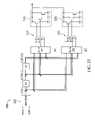
- FIG. 12shows a mechanism 200 , connected with device 100 of FIG. 8 , that can be used to equalize inductive or capacitive crosstalk errors created by signals in line 128 and felt in lines that are adjacent line 128 , the adjacent lines not shown in this figure.
- a first crosstalk equalization driver 205receives signals along lines P 1 , P 2 and P 3 that have been inverted by inverters 210 , controlling current sources 211 , 212 and 213 . The combined current from those current sources 211 , 212 and 213 is output on a crosstalk equalization line 220 that is connected to an adjacent line, not shown, the adjacent line subjected to crosstalk errors from line 128 .
- the output on line 220 from driver 205is thus scaled and inverted compared to the signal produced by main driver 105 , much like signal 160 of FIG. 11D is a scaled and inverted compared to signal 150 in FIG. 11A .
- a second crosstalk equalization driver 225receives input signals along lines X 1 , X 2 and X 3 that have been delayed by delay 110 , lines X 1 , X 2 and X 3 controlling current sources 221 , 222 and 223 .
- the output of second crosstalk equalization driver 225 on line 220is delayed and scaled compared to the signals produced by main driver 105 , much like signal 162 of FIG. 11E is scaled and delayed compared to signal 150 in FIG. 11A .
- the combined output of crosstalk equalization drivers 205 and 225 on line 220is much like signal 155 of FIG. 11C , which can be used to compensate for transient signal 152 of FIG. 11B .
- crosstalk equalization drivers 205 and 225can compensate for crosstalk inflicted by line 128 on nearby lines.
- An advantage of the circuit shown in FIG. 12is that cost and space effective circuits are implemented that generate equalization signals by tapping into the input signals for the main signal driver, instead of generating equalizing signals based upon the output signals that are transmitted.
- Similar equalization mechanismscan be used to compensate for reflections in a transmission line due to impedance discontinuities in the line. These reflections may be positive or negative, and may occur at various times relative to the main signal. Thus for example a known reflection may occur at a receiver with a delay of two clock cycles, for which plural unit delay elements may be provided between the input signals and the compensation circuits.
- unit delay elementsmay be provided for example by flip-flops, whereas delay elements that generate delays of less than a bit period may be provided for instance by inverters.
- FIG. 13shows another mechanism for equalizing multi-PAM signals, however the equalization mechanism inputs, on two lines, the MSB and LSB signals, rather than inputting the three lines of thermometer code inputs.
- a unit delay element 230 receiving the MSB and LSBoutputs those signals with a delay substantially equal to one signal bit duration. Unit delay 230 allows comparison at transition mapping device 233 of the MSB and LSB with the previous MSB and LSB, to gauge the multi-PAM transition between the prior and current MSB and LSB.
- transition mapping device 233Based upon this transition, transition mapping device 233 outputs a three bit signal to current digital-analog converter (IDAC) 235 , which drives a compensation signal on line 237 , which in this example connects with a multi-PAM signal, not shown in this figure, to compensate for crosstalk on that other line.
- IDACcurrent digital-analog converter
- FIG. 14shows such a general equalization system that can be used to compensate for various signal imperfections, whether the imperfections are due to attenuation, crosstalk, or reflections.
- Input signals on lines C(N) that control a main driver M(N)pass through a number J of delay elements D 1 through DJ, each of which delay the input signals by one bit signal period.
- Various self-equalization drivers S(N) through S(N+J), each of which is proportional to main driver M(N),are tapped off the input signals at various delay times.
- the equalization drivers S(N) through S(N+J)may each have a gain that is a different fraction of that of the main driver, and may or may not invert the input signals, depending upon the particular equalization desired.
- FIG. 15illustrates a mechanism 600 for adjusting equalization parameters such as the magnitude, timing and sign of the equalization signal.
- An encoder 302provides input signals on lines C(N) to a main signal driver, not shown in this figure, the input signals also encountering delay elements D 1 and D 2 that delay the input signals C(N) by one unit delay each, to provide delayed signals on lines C(N+1) and C(N+2).
- Signals on lines C(N), C(N+1) and C(N+2)are input to multiplexers MUX 307 and MUX 308 , which choose, based upon selection lines S 1 and S 2 , which of input signals on lines C(N), C(N+1) and C(N+2) to input to equalization drivers 310 and 320 .
- equalization driversmay have different current gains.
- Exclusive OR gates 315 and 325can be controlled to invert or not to invert the input signals selected by multiplexers MUX 1 and MUX 2 .
- This systemcan be expanded to provide multiple equalization drivers, XOR gates, multiplexers and delay elements, which together afford a variety of combinations of scaling, timing and inversion of the input signals to produce a desired equalization.
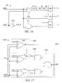
- FIG. 16shows the encoder 102 that converts MSB and LSB signals into input signals that are output on lines C 1 , C 2 and C 3 to control the output driver 105 .
- Datamay be transmitted and read at both rising and falling clock edges, so a pair of identical encoders may exist for translating MSB and LSB odd and even signals, with the encoders' output multiplexed on lines C 1 , C 2 and C 3 .
- the MSBis input to a latch 352 that also receives a transmit clock signal (TCLK) and complementary transmit clock signal (TCLK_B) for differentially latching the MSB as an input signal on line C 2 .
- the MSBis also input to an OR gate 340 that receives as the other input LSB.
- OR gate 340The output of OR gate 340 is latched at 350 , which outputs another input signal on line C 1 .
- the LSBpasses through inverter 348 to become LSB_B, which is input to an AND gate 344 that receives as the other input the MSB.
- the output of AND gate 344is clocked at 355 and output on line C 3 as a third input signal.
- the OR gate 340outputs on so that input signal C 1 is on, but C 2 and C 3 are still off.
- input signals C 1 and C 2are on, but AND gate 344 inputs LSB_B, which is low so the input signal on line C 3 is off.
- FIG. 17shows an integrating receiver 400 that may be used to receive the multi-level signals sent by drivers such as those described above, and decode the signals into MSB and LSB components.
- the datamay be transmitted at twice the clock frequency, and a pair of receivers 400 may read even and odd data.
- An MSB receiver 402 of the 4-PAM receiver 400 in this examplereceives and decodes a 4-PAM input signal VIN by determining whether the signal VIN is greater or less than VREFM.
- a latching comparator 404compares the value of the voltage of the received input signal VIN to the reference voltage VREFM and latches the value of the result of the comparison B in response to a receive clock signal.
- datais taken at both rising and falling clock edges.
- two latching comparators 410 and 414compare the value of the voltage of the received input signal VIN to the reference voltages VREFH and VREFL, and latch the value of the result of the comparison A and C, respectively, in response to the receive clock signal.
- the signals from the comparator outputs B, A, and Care then passed through combinational logic 420 .
- the latching comparators 404 , 410 and 414are implemented as integrating receivers to reduce the sensitivity of the output signal to noise.
- Errors generated by crosstalk or capacitive couplingmay be attenuated by the time they reach a receiver, which may in circuit board implementations be located up to about a foot away from the signal drivers, much as the transitions are attenuated over that distance. For crosstalk errors this attenuation may actually be beneficial as it tends to smooth out a high-frequency transient signal into a transient signal that may be compensated with an equalization having a duration of one bit. In a situation for which a neighbor's signal still has a high-frequency component when received, an integrating receiver can also smooth the data, so that compensating for a DC component of the crosstalk can be accomplished.
- FIG. 18Ashows a signal 450 undergoing a transition that may generate crosstalk in an adjacent line having a signal 452 shown in FIG. 18B .
- the crosstalkis apparent in FIG. 18B as a spike or high frequency component that is disturbing a step function transition.
- FIG. 18Cshows an equalization signal 455 designed to compensate for a DC component of the spike of FIG. 18B .
- Combination of signal 452 and compensating signal 455is shown in FIG. 18D as signal 457 , which may leave a dipole component of the spike uncompensated.
- FIG. 18Eshows that after integration by the receiver of FIG. 17 the dipole component has been removed, leaving a smooth transition signal 459 .
- crosstalkmay exist between each line and each nearby line.
- This crosstalkmay have characteristics, based upon how many lines are between the crosstalk creator and the crosstalk victim, which can be equalized with an FIR having corresponding equalization characteristics, such as magnitude, timing and sign. Since these crosstalk characteristics have a regular pattern, crosstalk FIRs for each line may have a number of standard equalization drivers each designed to compensate for crosstalk a certain number of lines away.
- self FIR 500 , self FIR 502 , self FIR 505 and self FIR 508may each have equal ratios k which can be used to compensate for attenuation and reflections.
- XTK 510 , XTK FIR 512 , XTK FIR 515 and XTK FIR 518may each have equal ratios k′ that depend upon whether a line being equalized is a first adjacent line, second adjacent line, third adjacent line or further spaced from the crosstalk generating and equalizing line.
- spaced signal lines S 1 , S 2 , S 3 and S 4may be grouped in pairs or other arrangements, for example with a ground wire disposed between the pairs of lines.
- crosstalk equalization FIRs 560 , 562 , 565 and 568may distinguish whether a signal line subjected to crosstalk from and adjacent signal line is spaced apart by a ground wire, and adjust the equalization parameters accordingly.
- lines that are adjacent in one area, such as at signal pads for a circuitmay be separated in another area, for example due to routing in separate layers of a circuit board.
- alternately spaced lines, such as S 1 and S 3may induce more crosstalk in each other than adjacent lines, such as S 1 and S 2 , and the equalization parameters may be adjusted accordingly.
- FIG. 21illustrates a memory system 600 in which embodiments of the present invention may be applied.
- the system 600includes a printed circuit board 601 (sometimes called a motherboard) to which a memory controller 603 , a signaling path 605 and connectors 607 A, 607 B are affixed.
- Memory modules 609 A, 609 B, each containing one or more memory devices 611are affixed to the printed circuit board 601 by being removably inserted into the connectors 607 A, 607 B.
- the memory modules 609 A, 609 Binclude traces to couple the memory devices 611 to the signaling path 605 and ultimately to the memory controller 603 .
- the signaling path 605constitutes a multi-drop bus that is coupled to each memory module.
- the individual memory devices of a given modulemay be coupled to the same set of signaling lines within signaling path 605 , or each memory device of the module may be coupled to a respective subset of the signaling lines. In the latter case, two or more memory devices 611 on a module may be accessed simultaneously to read or write a data value that is wider (i.e., contains more bits) than the data interface of a single memory device.
- each of the memory modulesmay be coupled to the memory controller via a dedicated signaling path (i.e., a point-to-point connection rather than a multi-drop bus).
- each of the memory devices on the memory modulemay be coupled to a shared set of signaling lines of the dedicated path, or each memory device may be coupled to respective subsets of the signaling lines.
- the signaling path 605may include a single, multiplexed set of signal lines to transfer both data and control information between the memory controller 603 and memory devices 611 .
- the signaling path 605may include a set of signaling lines for transferring data between the memory devices 611 and the memory controller 603 , and a separate set of signaling lines for transferring timing and control information between the memory devices 611 and the memory controller 603 (e.g., clock signals, read/write commands, and address information).
- the control informationis uni-directional, flowing from the memory controller 603 to the memory devices 611 , but status information may also be communicated from the memory devices 611 to the memory controller.
- the timing informationmay be generated within the memory controller 611 , or by external circuitry (not shown).
- selected signaling lines within signaling path 605are used to carry multi-level signals (e.g., 4-PAM signals) between the memory devices 611 and the memory controller 603 .
- multi-level signalse.g., 4-PAM signals
- a set of driver circuits within the memory controller 603output multi-level signals onto the selected traces of the signaling path, with equalization and/or cross-talk cancellation being applied to each such signal as described above.
- Receiver circuits within the addressed memory device (or memory devices)receive the multi-level signals from the memory controller 603 and convert the signals into corresponding binary representations.
- driver circuits within the memory device 611output equalized and cross-talk-canceled multi-level signals onto the selected set of traces of the signaling path for receipt by receiver circuits within the memory controller 603 .
- Such multi-level signalingmay be used to transfer both data and control information between the memory controller 603 and the memory devices 611 , or multi-level signaling may be used for one type of information transfer (e.g., data or control), but not the other.
- the signaling technique used to transfer either data or control information (or both)may be dynamically switched between binary and multi-level signaling according to detected events, such as bandwidth demand, detection of a threshold error rate, and so forth.
- FIG. 21Although a memory system that includes connectors for removable insertion of memory modules is depicted in FIG. 21 , other system topologies may be used.
- the memory devicesneed not be disposed on memory modules, but rather may be individually coupled to the printed circuit board 601 .
- the memory devices, the memory controller and the signaling pathmay all be included within a single integrated circuit along with other circuitry (e.g., graphics control circuitry, digital signal processing circuitry, general purpose processing circuitry, etc.).
- the system of FIG. 21can be used in any number of electronic devices, including without limitation, computer systems, telephones, network devices (e.g., switch, router, interface card, etc.), handheld electronic devices, intelligent appliances.
Landscapes
- Engineering & Computer Science (AREA)
- Power Engineering (AREA)
- Computer Networks & Wireless Communication (AREA)
- Signal Processing (AREA)
- Cable Transmission Systems, Equalization Of Radio And Reduction Of Echo (AREA)
- Dc Digital Transmission (AREA)
Abstract
Description
The present invention relates to multi-level digital signaling, and in particular to techniques to equalize or compensate for errors that may otherwise be present in a multi-level, multi-line signaling system.
The use of multiple signal levels instead of binary signal levels is a known technique for increasing the data rate of a digital signaling system, without necessarily increasing the signal frequency of the system. Such multi-level signaling is sometimes known as multiple pulse amplitude modulation or multi-PAM, and has been implemented with radio or other long-distance wireless signaling systems.
Other long-distance uses for multi-PAM signaling include computer or telecommunication systems that employ Gigabit Ethernet over optical fiber (IEEE 802.3z) and over copper wires (IEEE 802.3ab), which use three and five signal levels, respectively, spaced symmetrically about and including ground. Equalization techniques for long-distance multi-level signaling systems such as those used in radio or telecommunication networks commonly include adaptive filters, which can change equalization characteristics adaptively to improve equalization accuracy or in response to changing conditions. The complexities of these equalization techniques can delay signaling by slight but tolerable amounts for these long-distance systems.
Multi-PAM is not traditionally used for communication between devices in close proximity or belonging to the same system, such as those connected to the same integrated circuit (IC) or printed circuit board (PCB). One reason for this may be that within such a system the characteristics of transmission lines, such as buses or signal lines, over which signals travel are tightly controlled, so that increases in data rate may be achieved by simply increasing data frequency. At higher frequencies, however, receiving devices may have a reduced ability to distinguish binary signals, so that dividing signals into smaller levels for multi-PAM is problematic. Multi-PAM may also be more difficult to implement in multi-drop bus systems (i.e., buses shared by multiple processing mechanisms), since the lower signal-to-noise ratio for such systems sometimes results in bit errors even for binary signals. Moreover, complex equalization techniques such as employed for long distance communication systems may not be feasible in a bus system for which low latency is a performance criterion.
The present invention is directed to low-latency equalization mechanisms for short-range communications systems. Such equalization mechanisms may compensate for signal attenuation along a transmission line, reflections due to impedance discontinuities along such a line, and crosstalk between adjacent lines. The equalization mechanisms may be particularly advantageous for multi-PAM communications systems.
Alternatively, the logical states can be arranged in binary (00, 01, 10, 11) or other order.
In one embodiment the communication system is employed for a memory bus, which may for instance include random access memory (RAM), like that disclosed in U.S. Pat. No. 5,243,703 to Farmwald et al., which is incorporated herein by reference. The multi-PAM communication and low-latency signal correction techniques disclosed herein may also be used for other contained systems, such as for communication between processors of a multiprocessor apparatus, or between a processor and a peripheral device, such as a disk drive controller or network interface card over an input/output bus.
Several characteristics are apparent from the table ofFIG. 6 . First note that for the received signals, the M multiplier is the complement of the S multiplier. Also note that the drive signal S multiplier is equal to the initial S multiplier, while the transition M multiplier is equal to the final M multiplier. Also note that the table depicted inFIG. 6 illustrates just one set of transition drive signals specific to a 4-PAM signaling system with a single error correction, and may be extrapolated to be used with communication systems having additional signal levels and additional error corrections. For instance, a similar table may be constructed to deal with signal reflections, although such reflections may be either positive or negative and may have a delay of more than one bit signal duration, as measured at the signal receiver.
Also receiving the input signals fromencoder 102 isdelay mechanism 118, which inverts and delays by one bit signal period the input signals to feed signals E1, E2 and E3 toauxiliary driver 120. Auxiliary drivercurrent sources current sources current source current sources main driver 105 outputs signal52 ofFIG. 7B ,auxiliary driver 120 outputs signal55 ofFIG. 7C , which is delayed, inverted and proportional to signal52. Thesignals line 128 to form the desiredsignal 50 ofFIG. 7A .
Referring again toFIG. 6 , themain driver 105 can be represented with the letter M and theauxiliary driver 120 with the letter S, with the numeral preceding each letter describing how many of the respective current sources are active. ThusFIG. 7B may represent the voltage driven by themain driver 105, which transitions from 3M to 0M at T=1, andFIG. 7C may represent the voltage driven by theauxiliary driver 120, which transitions from 0S to 3S at T=2. A ratio of the gain of the auxiliary driver, S, to that of the main driver, M, is termed k, the equalization coefficient of the auxiliary driver. The ratio k is less than one, and may range from about one percent to about fifty percent.
Althoughcurrent sources device 100 ofFIG. 8 would have a distortion, for example, if each of thecurrent sources Current sources
Auxiliary drivercurrent sources current sources current sources current sources current sources current sources current sources current sources
InFIG. 9 , thedrivers delay element 118 are represented as aFIR filter 130. Input signals from the encoder are sent to the filter, which operates on the signals with function M and delays, inverts and operates on the signals with function S, to output a filtered signal.
Equalization techniques similar to those described above for attenuation can be used to compensate for crosstalk and reflection errors.FIG. 10 andFIG. 11 show a general system for filtering errors on a line V(N) usingself equalization FIR 130 as described above and withcrosstalk equalization FIR 133 andcrosstalk equalization FIR 135 due to crosstalk from adjacent lines A1(N) through AJ(N), respectively, to produce equalized output V′(N).FIG. 11A shows astep function signal 150 in line A1that generates, as shown inFIG. 11B , atransient signal 152 in line V due to inductive coupling.FIG. 11C shows anequalization signal 155 that is generated by inputtingsignal 150 to crosstalkequalization FIR 133 to compensate fortransient signal 152. Capacitive crosstalk generated in line V from lines A1through AJcan be equalized in a similar fashion. Both inductive and capacitive crosstalk may generate a transient signal having a polarity dependent upon the location of the receiver compared to the location at which the transient signal was generated.FIG. 11D shows afirst signal component 160 that may be used to compensate for such an inductive or capacitive crosstalk error, which is a scaled and inverted function ofsignal 150 that generated the error.FIG. 11E shows asecond signal component 162 that may be added to thesignal 160 to create thecrosstalk equalization signal 155 ofFIG. 11C . Signal162 can be scaled or fractional function ofsignal 150 that is delayed one bit period.
A secondcrosstalk equalization driver 225 receives input signals along lines X1, X2 and X3 that have been delayed by delay110, lines X1, X2 and X3 controllingcurrent sources crosstalk equalization driver 225 on line220 is delayed and scaled compared to the signals produced bymain driver 105, much likesignal 162 ofFIG. 11E is scaled and delayed compared to signal150 inFIG. 11A . The combined output ofcrosstalk equalization drivers signal 155 ofFIG. 11C , which can be used to compensate fortransient signal 152 ofFIG. 11B . Thuscrosstalk equalization drivers line 128 on nearby lines. An advantage of the circuit shown inFIG. 12 is that cost and space effective circuits are implemented that generate equalization signals by tapping into the input signals for the main signal driver, instead of generating equalizing signals based upon the output signals that are transmitted.
Similar equalization mechanisms can be used to compensate for reflections in a transmission line due to impedance discontinuities in the line. These reflections may be positive or negative, and may occur at various times relative to the main signal. Thus for example a known reflection may occur at a receiver with a delay of two clock cycles, for which plural unit delay elements may be provided between the input signals and the compensation circuits. Moreover, although a 4-PAM signaling system is shown, additional signal levels are possible with the provision of additional current sources. Unit delay elements may be provided for example by flip-flops, whereas delay elements that generate delays of less than a bit period may be provided for instance by inverters.
Thus for MSB=0 and LSB=0, all the input signals are off. For MSB=0 and LSB=1, theOR gate 340 outputs on so that input signal C1 is on, but C2 and C3 are still off. When both MSB=1 and LSB=1, input signals C1 and C2 are on, but ANDgate 344 inputs LSB_B, which is low so the input signal on line C3 is off. When MSB=1 and LSB=0, input signals on all the lines C1, C2 and C3 are turned on. In this fashion the MSB and LSB may be combined as Gray code and translated to thermometer code input signals on lines C1, C2 and C3 that control the current sources to drive 4-PAM signals.
Errors generated by crosstalk or capacitive coupling may be attenuated by the time they reach a receiver, which may in circuit board implementations be located up to about a foot away from the signal drivers, much as the transitions are attenuated over that distance. For crosstalk errors this attenuation may actually be beneficial as it tends to smooth out a high-frequency transient signal into a transient signal that may be compensated with an equalization having a duration of one bit. In a situation for which a neighbor's signal still has a high-frequency component when received, an integrating receiver can also smooth the data, so that compensating for a DC component of the crosstalk can be accomplished.
As illustrated inFIG. 19 , in a system that has numerous closely spaced signal lines S1, S2, S3 and S4, such as a bus for a computer or similar device, crosstalk may exist between each line and each nearby line. This crosstalk may have characteristics, based upon how many lines are between the crosstalk creator and the crosstalk victim, which can be equalized with an FIR having corresponding equalization characteristics, such as magnitude, timing and sign. Since these crosstalk characteristics have a regular pattern, crosstalk FIRs for each line may have a number of standard equalization drivers each designed to compensate for crosstalk a certain number of lines away. Thusself FIR 500,self FIR 502,self FIR 505 andself FIR 508 may each have equal ratios k which can be used to compensate for attenuation and reflections. SimilarlyXTK 510,XTK FIR 512,XTK FIR 515 andXTK FIR 518 may each have equal ratios k′ that depend upon whether a line being equalized is a first adjacent line, second adjacent line, third adjacent line or further spaced from the crosstalk generating and equalizing line.
As shown inFIG. 20 spaced signal lines S1, S2, S3 and S4 may be grouped in pairs or other arrangements, for example with a ground wire disposed between the pairs of lines. In this case,crosstalk equalization FIRs
In the embodiment ofFIG. 21 , thesignaling path 605 constitutes a multi-drop bus that is coupled to each memory module. The individual memory devices of a given module may be coupled to the same set of signaling lines within signalingpath 605, or each memory device of the module may be coupled to a respective subset of the signaling lines. In the latter case, two ormore memory devices 611 on a module may be accessed simultaneously to read or write a data value that is wider (i.e., contains more bits) than the data interface of a single memory device. In an alternative embodiment (not shown), each of the memory modules may be coupled to the memory controller via a dedicated signaling path (i.e., a point-to-point connection rather than a multi-drop bus). In such an embodiment, each of the memory devices on the memory module may be coupled to a shared set of signaling lines of the dedicated path, or each memory device may be coupled to respective subsets of the signaling lines.
Thesignaling path 605 may include a single, multiplexed set of signal lines to transfer both data and control information between thememory controller 603 andmemory devices 611. Alternatively, thesignaling path 605 may include a set of signaling lines for transferring data between thememory devices 611 and thememory controller 603, and a separate set of signaling lines for transferring timing and control information between thememory devices 611 and the memory controller603 (e.g., clock signals, read/write commands, and address information). Preferably the control information is uni-directional, flowing from thememory controller 603 to thememory devices 611, but status information may also be communicated from thememory devices 611 to the memory controller. Also, the timing information may be generated within thememory controller 611, or by external circuitry (not shown).
In one embodiment, selected signaling lines within signalingpath 605 are used to carry multi-level signals (e.g., 4-PAM signals) between thememory devices 611 and thememory controller 603. For transfers from thememory controller 603 to a givenmemory device 611, a set of driver circuits within thememory controller 603 output multi-level signals onto the selected traces of the signaling path, with equalization and/or cross-talk cancellation being applied to each such signal as described above. Receiver circuits within the addressed memory device (or memory devices) receive the multi-level signals from thememory controller 603 and convert the signals into corresponding binary representations. Conversely, for transfers from thememory device 611 to memory controller603 (e.g., in response to a read command issued to thememory device 611 by the memory controller603), driver circuits within thememory device 611 output equalized and cross-talk-canceled multi-level signals onto the selected set of traces of the signaling path for receipt by receiver circuits within thememory controller 603. Such multi-level signaling may be used to transfer both data and control information between thememory controller 603 and thememory devices 611, or multi-level signaling may be used for one type of information transfer (e.g., data or control), but not the other. Further, the signaling technique used to transfer either data or control information (or both) may be dynamically switched between binary and multi-level signaling according to detected events, such as bandwidth demand, detection of a threshold error rate, and so forth.
Although a memory system that includes connectors for removable insertion of memory modules is depicted inFIG. 21 , other system topologies may be used. For example, the memory devices need not be disposed on memory modules, but rather may be individually coupled to the printedcircuit board 601. Also, the memory devices, the memory controller and the signaling path may all be included within a single integrated circuit along with other circuitry (e.g., graphics control circuitry, digital signal processing circuitry, general purpose processing circuitry, etc.). The system ofFIG. 21 can be used in any number of electronic devices, including without limitation, computer systems, telephones, network devices (e.g., switch, router, interface card, etc.), handheld electronic devices, intelligent appliances.
Although we have focused on teaching the preferred embodiments of a low latency multi-line, multi-level equalized communication system, other embodiments and modifications of this invention will be apparent to persons of ordinary skill in the art in view of these teachings.
Therefore, this invention is limited only by the following claims, which include all such embodiments, modifications and equivalents when viewed in conjunction with the above specification and accompanying drawings.
Claims (29)
1. A communication system comprising:
a first printed circuit board;
a conductive path affixed to the printed circuit board;
a driver circuit affixed to the first printed circuit board and coupled to the conductive path to output onto the conductive path a signal having a voltage level that varies in time between at least three distinct levels representative of at least three distinct digital values, the driver circuit including an equalization circuit to adjust the voltage level of the signal output by the driver circuit at a first time according to a digital value represented by the signal at a previous time; and
a receiver circuit affixed to the first printed circuit board and coupled to receive the signal from the conductive path to determine which of the at least three distinct digital values is represented by the signal at a given time.
2. The system ofclaim 1 , wherein the driver and receiver circuits are respective integrated circuits affixed to the first printed circuit board.
3. The system ofclaim 1 , wherein the driver and receiver circuits and conductive path are incorporated within a common integrated circuit that is affixed to the first printed circuit board.
4. The system ofclaim 1 , wherein at least one of the driver and receiver circuits is coupled to a second printed circuit board that is affixed to the first printed circuit board.
5. The system ofclaim 4 , wherein the second printed circuit board is removably affixed to the first printed circuit board.
6. The system ofclaim 1 , wherein the driver circuit receives a plurality of input signals, and the equalization circuit receives and delays said plurality of input signals.
7. The system ofclaim 1 , wherein the driver circuit receives a plurality of input signals, and the equalization circuit receives and inverts said plurality of input signals.
8. The system ofclaim 1 , wherein the equalization circuit compensates for attenuation of the signal in the conductive path.
9. The system ofclaim 1 , wherein the equalization circuit compensates for reflection of the signal in the conductive path.
10. The system ofclaim 1 , wherein the equalization circuit compensates for crosstalk generated by the signal in a second conductive path.
11. The system ofclaim 1 , wherein said signal has a fourth voltage level that varies in time between at least three distinct levels, the fourth level representative of a fourth digital value that is distinct from the at least three distinct digital values.
12. A communication system comprising:
a main driver adapted to convert a plurality of binary input signals into a main signal that shifts over time between a plurality of signal levels representing respective ones of at least three logical states; and
an equalization mechanism containing an auxiliary driver adapted to receive said plurality of binary input signals and to generate an equalization signal, said equalization signal being combined with the main signal to form an output signal in which a respective transition between two different signal levels is overdriven by an amount depending on the two different signal levels.
13. The system ofclaim 12 , wherein said equalization mechanism includes an element adapted to invert said input signals.
14. The system ofclaim 12 , wherein said main driver and said auxiliary driver each include a current source, and said signal levels are voltages that are in a range between ground and a positive voltage.
15. The system ofclaim 12 , wherein said equalization mechanism is configured to compensate for attenuation of said signal over a signal line.
16. The system ofclaim 12 , wherein said equalization mechanism is configured to compensate for reflection of said signal over a signal line.
17. The system ofclaim 12 , wherein said signal is transmitted over a first signal line and creates crosstalk in a second signal line, and said equalization mechanism is coupled between said first and second lines and configured to compensate for said crosstalk in said second line.
18. The system ofclaim 12 , wherein the amount a respective transition in the output signal is overdriven is proportional to a transition magnitude of the respective transition.
19. The system ofclaim 12 , wherein the auxiliary driver includes an element adapted to delay said plurality of binary input signals by a time substantially equal to a bit period.
20. The system ofclaim 12 , wherein the auxiliary driver includes an element adapted to invert said plurality of binary input signals.
21. The system ofclaim 12 , wherein the main driver includes a plurality of driver current sources controlled by respective ones of the plurality of binary input signals and the auxiliary driver includes a plurality of driver current sources controlled by respective ones of delayed and inverted versions of the plurality of binary input signals, a respective driver current source in the auxiliary driver having a gain that is a fraction of a gain of a corresponding driver current source in the main driver.
22. The system ofclaim 12 , wherein output signal is transmitted on a first transmission line among a plurality of transmission lines, the system further comprising a first crosstalk equalization driver to receive inverted versions of the plurality of binary input signals and to output a first crosstalk equalization signal on a second transmission line adjacent the first transmission line.
23. The system ofclaim 22 , further comprising a second crosstalk equalization driver to receive delayed versions of the plurality of binary input signals and to output a second crosstalk equalization signal that is combined with the first crosstalk equalization signal.
24. A communication system comprising:
a signaling device configured to produce a set of signal levels representing a set of at least three logical states, said device including a main driver adapted to convert a plurality of binary input signals into an output signal that shifts over time between said signal levels to shift between said at least three logical states; and
an equalization mechanism containing an auxiliary driver that is substantially proportional to said main driver, said equalization mechanism adapted to receive said plurality of binary input signals and generate a set of at least three equalization signals based on said plurality of binary input signals;
wherein for each of said signal levels, an activation level of said main driver and an activation level of said auxiliary driver sum to equal N.
25. A communication system comprising:
a signaling device configured to produce a set of signal levels representing a set of at least three logical states, said device including a main driver adapted to convert a plurality of binary input signals into an output signal that shifts over time between said signal levels to shift between said at least three logical states; and
an equalization mechanism containing an auxiliary driver that is substantially proportional to said main driver, said equalization mechanism adapted to receive said plurality of binary input signals and generate a set of at least three equalization signals based on said plurality of binary input signals;
wherein said equalization mechanism includes an element adapted to delay said input signals by a time substantially equal to a bit period.
26. A communication system comprising:
a first main driver adapted to receive a first plurality of input signals and to output on a first line a first signal that varies over time between N output levels based on said first plurality of input signals, and a second main driver adapted to receive a second plurality of input signals and to output on a second line a second signal that varies over time between N output levels based on said second plurality of input signals, said main drivers adapted to shift from a first of said signal levels to a second of said signal levels by a transition having N−1 possible values for each said first signal level, said transition being substantially equal to a multiple of a difference between adjacent signal levels, said signal levels representing a set of logical states; and
an equalization mechanism including a first auxiliary driver having a gain that is substantially proportional to and smaller than said first main driver, said equalization mechanism configured to receive said first plurality of input signals and to output on said second line a third signal, whereby said third signal compensates for crosstalk on said second line generated by said first signal.
27. The system ofclaim 26 , wherein said main drivers and equalization mechanism each include a current source, and said signal levels are voltages that are in a range between ground and a positive voltage.
28. The system ofclaim 26 , wherein said equalization mechanism further comprises a delay element and a second auxiliary driver having a gain that is substantially proportional to and smaller than said first main driver, said second auxiliary driver configured to receive said first plurality of input signals after delay by said delay element, and to output on said first line a fourth signal.
29. The system ofclaim 26 , wherein said equalization mechanism further comprises an inversion element and a second auxiliary driver having a gain that is substantially proportional to and smaller than said first main driver, said second auxiliary driver configured to receive said first plurality of input signals after inversion by said inversion element, and to output on said first line a fourth signal.
Priority Applications (8)
| Application Number | Priority Date | Filing Date | Title |
|---|---|---|---|
| US09/654,643US7269212B1 (en) | 2000-09-05 | 2000-09-05 | Low-latency equalization in multi-level, multi-line communication systems |
| AU2001287074AAU2001287074A1 (en) | 2000-09-05 | 2001-09-05 | Calibration of a multi-level current mode driver |
| EP01966571AEP1410588B1 (en) | 2000-09-05 | 2001-09-05 | Communication system, multilevel signal and mulitlevel signal driver using equalization or crosstalk cancellation |
| AT01966571TATE463911T1 (en) | 2000-09-05 | 2001-09-05 | COMMUNICATION SYSTEM, MULTI-LEVEL SIGNAL AND MULTI-LEVEL SIGNAL DRIVER WITH EQUALIZATION OR CROSSTALK CANCELATION |
| DE60141775TDE60141775D1 (en) | 2000-09-05 | 2001-09-05 | Communication system, multi-level signal and multi-level signal driver with equalization or crosstalk cancellation |
| PCT/US2001/027478WO2002021782A2 (en) | 2000-09-05 | 2001-09-05 | Calibration of a multi-level current mode driver |
| US09/964,911US7072415B2 (en) | 1999-10-19 | 2001-09-27 | Method and apparatus for generating multi-level reference voltage in systems using equalization or crosstalk cancellation |
| US11/455,252US8320494B2 (en) | 1999-10-19 | 2006-06-15 | Method and apparatus for generating reference voltage to adjust for attenuation |
Applications Claiming Priority (1)
| Application Number | Priority Date | Filing Date | Title |
|---|---|---|---|
| US09/654,643US7269212B1 (en) | 2000-09-05 | 2000-09-05 | Low-latency equalization in multi-level, multi-line communication systems |
Related Parent Applications (1)
| Application Number | Title | Priority Date | Filing Date |
|---|---|---|---|
| US09/655,010Continuation-In-PartUS6772351B1 (en) | 1999-10-19 | 2000-09-05 | Method and apparatus for calibrating a multi-level current mode driver |
Related Child Applications (2)
| Application Number | Title | Priority Date | Filing Date |
|---|---|---|---|
| US09/655,010Continuation-In-PartUS6772351B1 (en) | 1999-10-19 | 2000-09-05 | Method and apparatus for calibrating a multi-level current mode driver |
| US09/964,911Continuation-In-PartUS7072415B2 (en) | 1999-10-19 | 2001-09-27 | Method and apparatus for generating multi-level reference voltage in systems using equalization or crosstalk cancellation |
Publications (1)
| Publication Number | Publication Date |
|---|---|
| US7269212B1true US7269212B1 (en) | 2007-09-11 |
Family
ID=38473308
Family Applications (1)
| Application Number | Title | Priority Date | Filing Date |
|---|---|---|---|
| US09/654,643Expired - LifetimeUS7269212B1 (en) | 1999-10-19 | 2000-09-05 | Low-latency equalization in multi-level, multi-line communication systems |
Country Status (3)
| Country | Link |
|---|---|
| US (1) | US7269212B1 (en) |
| AT (1) | ATE463911T1 (en) |
| DE (1) | DE60141775D1 (en) |
Cited By (127)
| Publication number | Priority date | Publication date | Assignee | Title |
|---|---|---|---|---|
| US20060170453A1 (en)* | 1999-10-19 | 2006-08-03 | Zerbe Jared L | Low latency multi-level communication interface |
| US20080069197A1 (en)* | 2006-09-20 | 2008-03-20 | Agere Systems Inc. | Equalizer for equalizing multiple received versions of a signal |
| US20080075159A1 (en)* | 2006-09-21 | 2008-03-27 | Uwe Sontowski | Receiver having multiple stages of equalization with tap coefficient copying |
| US20080205503A1 (en)* | 2007-02-23 | 2008-08-28 | Cooke Matthew E | Adaptive equalizer with tap coefficient averaging |
| US20090059703A1 (en)* | 2007-09-04 | 2009-03-05 | Hynix Semiconductor, Inc. | Receiver circuit of semiconductor memory apparatus |
| US20090060083A1 (en)* | 2007-09-04 | 2009-03-05 | Hynix Semiconductor, Inc. | Receiver circuit |
| US20090060017A1 (en)* | 2002-07-12 | 2009-03-05 | Rambus Inc. | Selectable-Tap Equalizer |
| US20090067278A1 (en)* | 2007-09-07 | 2009-03-12 | Hynix Semiconductor, Inc. | data output circuit for semiconductor memory apparatus |
| US20090080506A1 (en)* | 2006-01-12 | 2009-03-26 | Agere Systems Inc. | Receiver employing non-pilot reference channels for equalizing a received signal |
| US20090122904A1 (en)* | 2007-11-13 | 2009-05-14 | Samsung Electronics Co., Ltd. | Apparatuses and method for multi-level communication |
| US20090252212A1 (en)* | 2008-04-02 | 2009-10-08 | Sun Microsystems, Inc. | Method and apparatus for equalizing a high speed serial data link |
| US20100090721A1 (en)* | 2008-10-14 | 2010-04-15 | Hynix Semiconductor Inc. | Buffer of semiconductor memory apparatus |
| US20100118619A1 (en)* | 2008-11-13 | 2010-05-13 | Hynix Semiconductor Inc. | Buffer circuit of semiconductor memory apparatus |
| US20100308866A1 (en)* | 2009-06-08 | 2010-12-09 | Hynix Semiconductor Inc. | Semiconductor buffer circuit |
| US20130002225A1 (en)* | 2011-06-30 | 2013-01-03 | Broadcom Corporation | Current-Mode Active Termination |
| WO2013066774A1 (en)* | 2011-11-01 | 2013-05-10 | Rambus Inc. | Data transmission using delayed timing signals |
| US8861667B1 (en) | 2002-07-12 | 2014-10-14 | Rambus Inc. | Clock data recovery circuit with equalizer clock calibration |
| US20150146766A1 (en)* | 2012-11-30 | 2015-05-28 | Broadcom Corporation | Use of multi-level modulation signaling for short reach data communications |
| US20150280950A1 (en)* | 2014-03-26 | 2015-10-01 | Universiteit Gent | Signal Processing |
| US9166650B2 (en) | 2008-07-02 | 2015-10-20 | Rambus Inc. | Capacitive-coupled crosstalk cancellation |
| US9362962B2 (en) | 2010-05-20 | 2016-06-07 | Kandou Labs, S.A. | Methods and systems for energy-efficient communications interface |
| US9361223B1 (en) | 2012-05-14 | 2016-06-07 | Kandou Labs, S.A. | Storage method and apparatus for random access memory using codeword storage |
| US9413384B1 (en) | 2010-05-20 | 2016-08-09 | Kandou Labs, S.A. | Efficient processing and detection of balanced codes |
| US9424908B2 (en) | 2010-12-30 | 2016-08-23 | Kandou Labs, S.A. | Differential vector storage for dynamic random access memory |
| US9450744B2 (en) | 2010-05-20 | 2016-09-20 | Kandou Lab, S.A. | Control loop management and vector signaling code communications links |
| US9450791B2 (en) | 2010-05-20 | 2016-09-20 | Kandoub Lab, S.A. | Circuits for efficient detection of vector signaling codes for chip-to-chip communication |
| US9485057B2 (en) | 2010-05-20 | 2016-11-01 | Kandou Labs, S.A. | Vector signaling with reduced receiver complexity |
| US9544015B2 (en)* | 2014-06-25 | 2017-01-10 | Kandou Labs, S.A. | Multilevel driver for high speed chip-to-chip communications |
| US9553742B1 (en)* | 2015-09-15 | 2017-01-24 | Inphi Corporation | Method and apparatus for independent rise and fall waveform shaping |
| US9557760B1 (en) | 2015-10-28 | 2017-01-31 | Kandou Labs, S.A. | Enhanced phase interpolation circuit |
| US9577815B1 (en) | 2015-10-29 | 2017-02-21 | Kandou Labs, S.A. | Clock data alignment system for vector signaling code communications link |
| US9607673B1 (en) | 2010-05-20 | 2017-03-28 | Kandou Labs S.A. | Methods and systems for pin-efficient memory controller interface using vector signaling codes for chip-to-chip communication |
| US9654310B1 (en)* | 2016-11-19 | 2017-05-16 | Nxp Usa, Inc. | Analog delay cell and tapped delay line comprising the analog delay cell |
| US9667379B2 (en) | 2010-06-04 | 2017-05-30 | Ecole Polytechnique Federale De Lausanne (Epfl) | Error control coding for orthogonal differential vector signaling |
| US9674014B2 (en) | 2014-10-22 | 2017-06-06 | Kandou Labs, S.A. | Method and apparatus for high speed chip-to-chip communications |
| US9686106B2 (en) | 2014-02-28 | 2017-06-20 | Kandou Labs, S.A. | Clock-embedded vector signaling codes |
| US9686107B2 (en) | 2010-05-20 | 2017-06-20 | Kandou Labs, S.A. | Methods and systems for chip-to-chip communication with reduced simultaneous switching noise |
| US9692381B2 (en) | 2014-05-16 | 2017-06-27 | Kandou Labs, S.A. | Symmetric linear equalization circuit with increased gain |
| US9755870B1 (en)* | 2016-03-04 | 2017-09-05 | Inphi Corporation | Eye modulation for pulse-amplitude modulation communication systems |
| US9825677B2 (en) | 2010-04-30 | 2017-11-21 | ECOLE POLYTECHNIQUE FéDéRALE DE LAUSANNE | Orthogonal differential vector signaling |
| US9825723B2 (en) | 2010-05-20 | 2017-11-21 | Kandou Labs, S.A. | Methods and systems for skew tolerance in and advanced detectors for vector signaling codes for chip-to-chip communication |
| US9832046B2 (en) | 2015-06-26 | 2017-11-28 | Kandou Labs, S.A. | High speed communications system |
| US9838017B2 (en) | 2010-05-20 | 2017-12-05 | Kandou Labs, S.A. | Methods and systems for high bandwidth chip-to-chip communcations interface |
| US9838234B2 (en) | 2014-08-01 | 2017-12-05 | Kandou Labs, S.A. | Orthogonal differential vector signaling codes with embedded clock |
| US9893911B2 (en) | 2014-07-21 | 2018-02-13 | Kandou Labs, S.A. | Multidrop data transfer |
| US9906358B1 (en) | 2016-08-31 | 2018-02-27 | Kandou Labs, S.A. | Lock detector for phase lock loop |
| US9985745B2 (en) | 2013-06-25 | 2018-05-29 | Kandou Labs, S.A. | Vector signaling with reduced receiver complexity |
| US10003424B2 (en) | 2014-07-17 | 2018-06-19 | Kandou Labs, S.A. | Bus reversible orthogonal differential vector signaling codes |
| US10003315B2 (en) | 2016-01-25 | 2018-06-19 | Kandou Labs S.A. | Voltage sampler driver with enhanced high-frequency gain |
| US10003454B2 (en) | 2016-04-22 | 2018-06-19 | Kandou Labs, S.A. | Sampler with low input kickback |
| US10056903B2 (en) | 2016-04-28 | 2018-08-21 | Kandou Labs, S.A. | Low power multilevel driver |
| US10057049B2 (en) | 2016-04-22 | 2018-08-21 | Kandou Labs, S.A. | High performance phase locked loop |
| US10055372B2 (en) | 2015-11-25 | 2018-08-21 | Kandou Labs, S.A. | Orthogonal differential vector signaling codes with embedded clock |
| US10091035B2 (en) | 2013-04-16 | 2018-10-02 | Kandou Labs, S.A. | Methods and systems for high bandwidth communications interface |
| US10116468B1 (en) | 2017-06-28 | 2018-10-30 | Kandou Labs, S.A. | Low power chip-to-chip bidirectional communications |
| US10153591B2 (en) | 2016-04-28 | 2018-12-11 | Kandou Labs, S.A. | Skew-resistant multi-wire channel |
| US10177812B2 (en) | 2014-01-31 | 2019-01-08 | Kandou Labs, S.A. | Methods and systems for reduction of nearest-neighbor crosstalk |
| US10200218B2 (en) | 2016-10-24 | 2019-02-05 | Kandou Labs, S.A. | Multi-stage sampler with increased gain |
| US10200188B2 (en) | 2016-10-21 | 2019-02-05 | Kandou Labs, S.A. | Quadrature and duty cycle error correction in matrix phase lock loop |
| US20190044762A1 (en)* | 2017-08-07 | 2019-02-07 | Micron Technology, Inc. | Programmable channel equalization for multi-level signaling |
| US10203226B1 (en) | 2017-08-11 | 2019-02-12 | Kandou Labs, S.A. | Phase interpolation circuit |
| US20190103148A1 (en)* | 2017-10-02 | 2019-04-04 | Micron Technology, Inc. | Multiplexing distinct signals on a single pin of a memory device |
| US10277431B2 (en) | 2016-09-16 | 2019-04-30 | Kandou Labs, S.A. | Phase rotation circuit for eye scope measurements |
| US10320588B2 (en) | 2014-07-10 | 2019-06-11 | Kandou Labs, S.A. | Vector signaling codes with increased signal to noise characteristics |
| US10326623B1 (en) | 2017-12-08 | 2019-06-18 | Kandou Labs, S.A. | Methods and systems for providing multi-stage distributed decision feedback equalization |
| US10333749B2 (en) | 2014-05-13 | 2019-06-25 | Kandou Labs, S.A. | Vector signaling code with improved noise margin |
| US10333741B2 (en) | 2016-04-28 | 2019-06-25 | Kandou Labs, S.A. | Vector signaling codes for densely-routed wire groups |
| US10348436B2 (en) | 2014-02-02 | 2019-07-09 | Kandou Labs, S.A. | Method and apparatus for low power chip-to-chip communications with constrained ISI ratio |
| US10372665B2 (en) | 2016-10-24 | 2019-08-06 | Kandou Labs, S.A. | Multiphase data receiver with distributed DFE |
| US10403337B2 (en) | 2017-08-07 | 2019-09-03 | Micron Technology, Inc. | Output driver for multi-level signaling |
| US10439661B1 (en)* | 2017-02-19 | 2019-10-08 | Payam Heydari | Low-power high-speed signaling scheme over transmission line with unmatched terminations |
| US10447512B2 (en) | 2017-08-07 | 2019-10-15 | Micron Technology, Inc. | Channel equalization for multi-level signaling |
| US10446198B2 (en) | 2017-10-02 | 2019-10-15 | Micron Technology, Inc. | Multiple concurrent modulation schemes in a memory system |
| US10467177B2 (en) | 2017-12-08 | 2019-11-05 | Kandou Labs, S.A. | High speed memory interface |
| US10490245B2 (en) | 2017-10-02 | 2019-11-26 | Micron Technology, Inc. | Memory system that supports dual-mode modulation |
| US10496583B2 (en) | 2017-09-07 | 2019-12-03 | Kandou Labs, S.A. | Low power multilevel driver for generating wire signals according to summations of a plurality of weighted analog signal components having wire-specific sub-channel weights |
| US10515673B2 (en) | 2018-02-28 | 2019-12-24 | SK Hynix Inc. | Semiconductor devices and semiconductor systems including a semiconductor device |
| US10530616B2 (en) | 2015-09-29 | 2020-01-07 | Rambus Inc. | Transmitter with self-triggered transition equalizer |
| US10554380B2 (en) | 2018-01-26 | 2020-02-04 | Kandou Labs, S.A. | Dynamically weighted exclusive or gate having weighted output segments for phase detection and phase interpolation |
| US10574487B1 (en) | 2019-04-08 | 2020-02-25 | Kandou Labs, S.A. | Sampler offset calibration during operation |
| WO2020041048A1 (en)* | 2018-08-21 | 2020-02-27 | Micron Technology, Inc. | Pre-distortion for multi-level signaling |
| US10608849B1 (en) | 2019-04-08 | 2020-03-31 | Kandou Labs, S.A. | Variable gain amplifier and sampler offset calibration without clock recovery |
| US10623217B1 (en)* | 2019-05-29 | 2020-04-14 | Nvidia Corp. | Proportional AC-coupled edge-boosting transmit equalization for multi-level pulse-amplitude modulated signaling |
| KR20200040313A (en)* | 2017-10-02 | 2020-04-17 | 마이크론 테크놀로지, 인크 | Data communication with stacked memory die |
| US10666297B2 (en) | 2017-04-14 | 2020-05-26 | Kandou Labs, S.A. | Pipelined forward error correction for vector signaling code channel |
| US10679716B2 (en) | 2016-04-22 | 2020-06-09 | Kandou Labs, S.A. | Calibration apparatus and method for sampler with adjustable high frequency gain |
| US10680634B1 (en) | 2019-04-08 | 2020-06-09 | Kandou Labs, S.A. | Dynamic integration time adjustment of a clocked data sampler using a static analog calibration circuit |
| US10686634B2 (en) | 2017-08-07 | 2020-06-16 | Micron Technology, Inc | Multi-level signaling in memory with wide system interface |
| US10686583B2 (en) | 2017-07-04 | 2020-06-16 | Kandou Labs, S.A. | Method for measuring and correcting multi-wire skew |
| US10693587B2 (en) | 2017-07-10 | 2020-06-23 | Kandou Labs, S.A. | Multi-wire permuted forward error correction |
| US10693473B2 (en) | 2017-05-22 | 2020-06-23 | Kandou Labs, S.A. | Multi-modal data-driven clock recovery circuit |
| US10693688B2 (en) | 2017-12-28 | 2020-06-23 | Kandou Labs, S.A. | Synchronously-switched multi-input demodulating comparator |
| US10721106B1 (en) | 2019-04-08 | 2020-07-21 | Kandou Labs, S.A. | Adaptive continuous time linear equalization and channel bandwidth control |
| US10725913B2 (en) | 2017-10-02 | 2020-07-28 | Micron Technology, Inc. | Variable modulation scheme for memory device access or operation |
| US10742451B2 (en) | 2018-06-12 | 2020-08-11 | Kandou Labs, S.A. | Passive multi-input comparator for orthogonal codes on a multi-wire bus |
| US10771295B2 (en) | 2003-12-17 | 2020-09-08 | Rambus Inc. | High speed signaling system with adaptive transmit pre-emphasis |
| US10887137B2 (en) | 2019-03-15 | 2021-01-05 | Rambus Inc. | Edge enhancement for signal transmitter |
| US10931249B2 (en) | 2018-06-12 | 2021-02-23 | Kandou Labs, S.A. | Amplifier with adjustable high-frequency gain using varactor diodes |
| KR20210049182A (en)* | 2018-10-05 | 2021-05-04 | 마이크론 테크놀로지, 인크 | Dynamic configuration of the transmission line of the bus |
| US11183983B2 (en) | 2018-09-10 | 2021-11-23 | Kandou Labs, S.A. | Programmable continuous time linear equalizer having stabilized high-frequency peaking for controlling operating current of a slicer |
| US20220028448A1 (en)* | 2020-07-27 | 2022-01-27 | Micron Technology, Inc. | Apparatuses, systems, and methods for frequency-dependent signal modulation |
| US11240076B2 (en) | 2014-05-13 | 2022-02-01 | Kandou Labs, S.A. | Vector signaling code with improved noise margin |
| US11264832B2 (en)* | 2016-10-19 | 2022-03-01 | Sony Semiconductor Solutions Corporation | Signal processing device, signal processing method, and program |
| US11303484B1 (en) | 2021-04-02 | 2022-04-12 | Kandou Labs SA | Continuous time linear equalization and bandwidth adaptation using asynchronous sampling |
| US11374800B1 (en) | 2021-04-14 | 2022-06-28 | Kandou Labs SA | Continuous time linear equalization and bandwidth adaptation using peak detector |
| US11456708B1 (en) | 2021-04-30 | 2022-09-27 | Kandou Labs SA | Reference generation circuit for maintaining temperature-tracked linearity in amplifier with adjustable high-frequency gain |
| US11477059B2 (en) | 2020-12-09 | 2022-10-18 | Rambus Inc. | Circuits and methods for detecting and unlocking edge-phase lock |
| US11502681B2 (en) | 2018-12-04 | 2022-11-15 | Rambus Inc. | Method and system for balancing power-supply loading |
| KR20230000322A (en)* | 2021-06-24 | 2023-01-02 | 에스케이하이닉스 주식회사 | Electronic device performing for data align operation |
| JP2023017299A (en)* | 2021-07-26 | 2023-02-07 | 株式会社日立製作所 | Printed wiring board and information processing device |
| US11606229B2 (en) | 2017-08-07 | 2023-03-14 | Micron Technology, Inc. | Method to vertically align multi-level cell |
| US11831323B2 (en) | 2021-04-13 | 2023-11-28 | Cadence Design Systems, Inc. | Methods and circuits for reducing clock jitter |
| US11831472B1 (en) | 2022-08-30 | 2023-11-28 | Kandou Labs SA | Pre-scaler for orthogonal differential vector signalling |
| US11841815B1 (en) | 2021-12-31 | 2023-12-12 | Eliyan Corporation | Chiplet gearbox for low-cost multi-chip module applications |
| US11842986B1 (en) | 2021-11-25 | 2023-12-12 | Eliyan Corporation | Multi-chip module (MCM) with interface adapter circuitry |
| US11855056B1 (en) | 2019-03-15 | 2023-12-26 | Eliyan Corporation | Low cost solution for 2.5D and 3D packaging using USR chiplets |
| US11855043B1 (en) | 2021-05-06 | 2023-12-26 | Eliyan Corporation | Complex system-in-package architectures leveraging high-bandwidth long-reach die-to-die connectivity over package substrates |
| US12058874B1 (en) | 2022-12-27 | 2024-08-06 | Eliyan Corporation | Universal network-attached memory architecture |
| US12063034B2 (en) | 2022-08-30 | 2024-08-13 | Kandou Labs SA | Line driver impedance calibration for multi-wire data bus |
| US12182040B1 (en) | 2023-06-05 | 2024-12-31 | Eliyan Corporation | Multi-chip module (MCM) with scalable high bandwidth memory |
| US12190038B1 (en) | 2021-11-25 | 2025-01-07 | Eliyan Corporation | Multi-chip module (MCM) with multi-port unified memory |
| US12204482B1 (en) | 2023-10-09 | 2025-01-21 | Eliyan Corporation | Memory chiplet with efficient mapping of memory-centric interface to die-to-die (D2D) unit interface modules |
| US12204468B1 (en) | 2023-10-11 | 2025-01-21 | Eliyan Corporation | Universal memory interface with dynamic bidirectional data transfers |
| US12204794B1 (en) | 2021-05-18 | 2025-01-21 | Eliyan Corporation | Architecture for DRAM control optimization using simultaneous bidirectional memory interfaces |
| US12248419B1 (en) | 2022-05-26 | 2025-03-11 | Eliyan Corporation | Interface conversion circuitry for universal chiplet interconnect express (UCIe) |
| US12355409B2 (en) | 2022-03-24 | 2025-07-08 | Kandou Labs SA | Variable gain amplifier with cross-coupled common mode reduction |
| US12438095B1 (en) | 2021-05-06 | 2025-10-07 | Eliyan Corp. | Complex system-in-package architectures leveraging high-bandwidth long-reach die-to-die connectivity over package substrates |
Citations (190)
| Publication number | Priority date | Publication date | Assignee | Title |
|---|---|---|---|---|
| US2912684A (en) | 1953-01-23 | 1959-11-10 | Digital Control Systems Inc | Single channel transmission system |
| US3051901A (en) | 1958-06-24 | 1962-08-28 | Bell Telephone Labor Inc | Encoder for pulse code modulation |
| US3078378A (en) | 1960-06-28 | 1963-02-19 | Lockheed Aircraft Corp | Electronic multiplexer system for converting multi-channel data into a single channel composite signal |
| US3267459A (en) | 1962-12-18 | 1966-08-16 | Ibm | Data transmission system |
| US3484559A (en) | 1965-07-29 | 1969-12-16 | Post Office | Interstage signalling system using discrete currents or voltages |
| US3508076A (en) | 1967-04-26 | 1970-04-21 | Rca Corp | Logic circuitry |
| US3510585A (en) | 1967-02-02 | 1970-05-05 | Xerox Corp | Multi-level data encoder-decoder with pseudo-random test pattern generation capability |
| US3560856A (en) | 1966-12-29 | 1971-02-02 | Nippon Electric Co | Multilevel signal transmission system |
| US3569955A (en) | 1967-10-12 | 1971-03-09 | Lignes Telegraph Telephon | Method and devices for converting coded binary signals into multilevel signals and for reconverting the latter into the former |
| US3571725A (en) | 1967-05-25 | 1971-03-23 | Nippon Electric Co | Multilevel signal transmission system |
| US3587088A (en) | 1967-12-21 | 1971-06-22 | Bell Telephone Labor Inc | Multilevel pulse transmission systems employing codes having three or more alphabets |
| US3648064A (en) | 1968-07-01 | 1972-03-07 | Nippon Telegraph & Telephone | Multiple signal level high-speed logic circuit device |
| US3697874A (en) | 1966-12-29 | 1972-10-10 | Nippon Electric Co | Multilevel code conversion system |
| US3731199A (en) | 1971-04-30 | 1973-05-01 | Nippon Telegraph & Telephone | Multilevel signal transmission system |
| US3733550A (en) | 1971-04-30 | 1973-05-15 | Nippon Tt Public Corp | Multilevel signal transmission system |
| US3753113A (en) | 1970-06-20 | 1973-08-14 | Nippon Electric Co | Multilevel code signal transmission system |
| US3754237A (en) | 1971-03-05 | 1973-08-21 | Lignes Telegraph Telephon | Communication system using binary to multi-level and multi-level to binary coded pulse conversion |
| US3761818A (en) | 1971-04-30 | 1973-09-25 | Nippon Telegraph & Telephone | Multilevel signal transmission system |
| US3772680A (en) | 1970-07-31 | 1973-11-13 | Nippon Electric Co | Digital transmission channel monitoring system |
| US3798544A (en) | 1971-09-23 | 1974-03-19 | Int Standard Electric Corp | Multilevel pcm system enabling agc control of a transmitted multilevel signal in any selected frequency portion of said transmitted signal |
| US3832490A (en) | 1972-10-13 | 1974-08-27 | Co Ind Des Communication Cit A | Coder for increase of transmission speed |
| US3860871A (en) | 1972-06-09 | 1975-01-14 | Fujitsu Ltd | Phase control system for demodulation carrier in carrier band multilevel signal transmission |
| US3876944A (en) | 1967-07-27 | 1975-04-08 | Xerox Corp | Dibinary encoding technique |
| US3927401A (en) | 1972-11-24 | 1975-12-16 | Gen Motors Corp | Method and apparatus for coding and decoding digital data |
| US3978284A (en) | 1973-02-09 | 1976-08-31 | Nippon Hoso Kyokai | Receiver for use in a multi-level code transmission system |
| US3988676A (en) | 1971-05-17 | 1976-10-26 | Milgo Electronic Corporation | Coding and decoding system with multi-level format |
| US4038564A (en) | 1975-02-20 | 1977-07-26 | Casio Computer Co., Ltd. | Multi-level voltage selection circuit |
| US4070650A (en) | 1975-05-29 | 1978-01-24 | Kabushiki Kaisha Tokai Rika Denki Seisakusho | Digital signal transmission system and equipment |
| US4086587A (en) | 1977-02-28 | 1978-04-25 | Gte Automatic Electric Laboratories Incorporated | Apparatus and method for generating a high-accuracy 7-level correlative signal |
| US4097859A (en) | 1976-11-01 | 1978-06-27 | Burroughs Corporation | Three-level to two-level decoder |
| US4131761A (en) | 1976-04-22 | 1978-12-26 | Cselt - Centro Studi E Laboratori Telecomunicazioni | Method of and means for conveying and recovering supplementary message signals superimposed upon a multilevel signal stream in a digital transmission system |
| JPS5451343A (en) | 1977-09-30 | 1979-04-23 | Hitachi Ltd | Code converter |
| JPS5460850A (en) | 1977-10-24 | 1979-05-16 | Mitsubishi Electric Corp | Multi-level output device |
| USRE30182E (en) | 1969-06-24 | 1979-12-25 | Bell Telephone Laboratories, Incorporated | Precoded ternary data transmission |
| US4181865A (en) | 1977-04-28 | 1980-01-01 | Tokyo Shibaura Electric Co., Ltd. | Sensing circuit for a multi-level signal charge |
| US4280221A (en) | 1979-05-31 | 1981-07-21 | The Boeing Company | Digital data communication system |
| JPS56164650A (en) | 1980-05-21 | 1981-12-17 | Toshiba Corp | Input and output control system for data transmission |
| US4373152A (en) | 1980-12-22 | 1983-02-08 | Honeywell Information Systems Inc. | Binary to one out of four converter |
| JPS5854412A (en) | 1981-09-28 | 1983-03-31 | Hitachi Ltd | Voltage regulator for electric power supply |
| JPS5870662A (en) | 1981-10-23 | 1983-04-27 | Hitachi Ltd | digital integrated circuit |
| US4382249A (en) | 1980-12-22 | 1983-05-03 | Honeywell Information Systems Inc. | Apparatus and method for decoding information |
| US4403330A (en) | 1980-08-08 | 1983-09-06 | Siemens Aktiengesellschaft | Regenerative repeater for multi-stage digital signals |
| US4408189A (en) | 1981-05-18 | 1983-10-04 | Northern Telecom Limited | Method and apparatus for code conversion of binary to multilevel signals |
| US4408135A (en) | 1979-12-26 | 1983-10-04 | Tokyo Shibaura Denki Kabushiki Kaisha | Multi-level signal generating circuit |
| EP0094624A2 (en) | 1982-05-14 | 1983-11-23 | Siemens Aktiengesellschaft | Apparatus for generating quaternary signals |
| JPS5936465A (en) | 1982-08-23 | 1984-02-28 | Sony Corp | Digital data transmitting and receiving system |
| US4438491A (en) | 1980-10-14 | 1984-03-20 | Constant James N | Computer having plural IC chips with each chip including a transceiver |
| US4481625A (en) | 1981-10-21 | 1984-11-06 | Elxsi | High speed data bus system |
| JPS6087551A (en) | 1983-10-20 | 1985-05-17 | Fujitsu Ltd | Multilevel transmission method |
| US4528550A (en) | 1983-10-31 | 1985-07-09 | Northern Telecom Limited | Method and apparatus for code conversion of binary of multilevel signals |
| JPS60194647A (en) | 1984-03-16 | 1985-10-03 | Hitachi Ltd | Data transmission system |
| US4571735A (en) | 1981-10-08 | 1986-02-18 | Furse Anthony G | Method of multi-level encoding including synchronizing signals |
| US4602374A (en) | 1984-02-27 | 1986-07-22 | Nippon Telegraph & Telephone Public Corporation | Multi-level decision circuit |
| US4620188A (en) | 1981-08-17 | 1986-10-28 | Development Finance Corporation Of New Zealand | Multi-level logic circuit |
| US4628297A (en) | 1984-02-01 | 1986-12-09 | Hitachi, Ltd. | Code modulation system |
| JPS6251329A (en) | 1985-08-30 | 1987-03-06 | Nec Corp | Code identification circuit |
| US4748637A (en) | 1985-11-29 | 1988-05-31 | Conklin Instrument Corporation | Digital subscriber loop termination device |
| US4779073A (en) | 1986-04-24 | 1988-10-18 | Matsushita Electric Industrial Co., Ltd. | Apparatus for 3B-2T code conversion |
| US4805190A (en) | 1986-07-28 | 1989-02-14 | Alcatel Cit | Detector logic circuit for a sychronous transmission system for data comprising ternary symbols and controlled partial response class 1, N=2 type intersymbol interference |
| US4821286A (en) | 1986-05-27 | 1989-04-11 | American Telephone And Telegraph Company | Quaternary signal regenerator |
| US4823028A (en) | 1987-12-04 | 1989-04-18 | Tektronix, Inc. | Multilevel logic circuit with floating node voltage clamp |
| US4825450A (en) | 1987-03-12 | 1989-04-25 | The Boeing Company | Binary data communication system |
| US4841301A (en) | 1984-03-30 | 1989-06-20 | Nec Corporation | Device operable like an automatic level control circuit for decoding a multivalued signal |
| US4860309A (en) | 1986-09-17 | 1989-08-22 | Costello John F | Trinary bus communication system |
| US4875049A (en) | 1984-11-06 | 1989-10-17 | Nec Corporation | Automatic level control circuit for an ad convertor |
| US4888764A (en) | 1986-12-11 | 1989-12-19 | Siemens Aktiengesellschaft | Transmission-reception equipment for a bus system |
| EP0352869A2 (en) | 1988-07-29 | 1990-01-31 | Shell Internationale Researchmaatschappij B.V. | Modal transmission method and apparatus for multi-conductor wireline cables |
| JPH02128201A (en) | 1988-11-09 | 1990-05-16 | Fuji Electric Co Ltd | programmable controller |
| JPH02140676A (en) | 1988-11-21 | 1990-05-30 | Advantest Corp | Multilevel driving circuit |
| US5003555A (en) | 1987-06-09 | 1991-03-26 | U.S. Philips Corporation | Data transmission system comprising a decision feedback equalizer and using partial-response techniques |
| US5023841A (en) | 1988-02-26 | 1991-06-11 | International Business Machines Corporation | Double stage sense amplifier for random access memories |
| US5023488A (en) | 1990-03-30 | 1991-06-11 | Xerox Corporation | Drivers and receivers for interfacing VLSI CMOS circuits to transmission lines |
| US5045728A (en) | 1989-05-17 | 1991-09-03 | Ncr Corporation | Trinary to binary level conversion circuit |
| US5046050A (en) | 1990-04-10 | 1991-09-03 | National Semiconductor Corporation | Shared BiCMOS sense amplifier |
| EP0463316A1 (en) | 1990-06-07 | 1992-01-02 | International Business Machines Corporation | Self-adjusting impedance matching driver |
| JPH0444691A (en) | 1990-06-12 | 1992-02-14 | Seiko Instr Inc | Memory device |
| EP0482392A2 (en) | 1990-10-26 | 1992-04-29 | Alcatel SEL Aktiengesellschaft | Circuit arrangement for providing an output current for a data driver |
| US5115450A (en) | 1989-07-06 | 1992-05-19 | Advanced Micro Devices, Inc. | High speed digital to analog to digital communication system |
| US5121411A (en) | 1990-07-24 | 1992-06-09 | Motorola, Inc. | Multi-edge clock recovery method |
| EP0490504A2 (en) | 1990-12-12 | 1992-06-17 | Nortel Networks Corporation | Multilevel line coding scheme |
| US5126974A (en) | 1989-01-20 | 1992-06-30 | Hitachi, Ltd. | Sense amplifier for a memory device |
| US5153459A (en) | 1987-06-20 | 1992-10-06 | Samsung Electronics Co., Ltd. | Data transmission circuit for data buses including feedback circuitry |
| US5172338A (en) | 1989-04-13 | 1992-12-15 | Sundisk Corporation | Multi-state EEprom read and write circuits and techniques |
| US5194765A (en) | 1991-06-28 | 1993-03-16 | At&T Bell Laboratories | Digitally controlled element sizing |
| JPH05143211A (en) | 1991-11-18 | 1993-06-11 | Omron Corp | Input interface circuit |
| US5230008A (en) | 1991-01-18 | 1993-07-20 | Motorola, Inc. | Multi-amplitude sample generating apparatus and method |
| US5243625A (en) | 1990-07-16 | 1993-09-07 | U.S. Philips Corporation | Receiver for multivalued digital signals |
| US5254883A (en) | 1992-04-22 | 1993-10-19 | Rambus, Inc. | Electrical current source circuitry for a bus |
| US5259002A (en) | 1990-08-02 | 1993-11-02 | Carlstedt Elektronik Ab | Communication link |
| US5280500A (en) | 1991-10-10 | 1994-01-18 | Crescendo Communications, Inc. | Method and apparatus for multilevel encoding for a local area network |
| US5287108A (en) | 1992-07-02 | 1994-02-15 | National Semiconductor Corporation | Multistep analog-to-digital converter with successive approximation register circuit for least significant bit resolution |
| US5295157A (en) | 1991-06-04 | 1994-03-15 | Sony Corporation | Equalization method utilizing a delay circuit |
| US5295155A (en) | 1992-10-30 | 1994-03-15 | International Business Machines Corporation | Multi-level digital data regeneration system |
| US5315175A (en) | 1993-03-18 | 1994-05-24 | Northern Telecom Limited | Quasi-differential bus |
| US5331320A (en) | 1991-11-21 | 1994-07-19 | International Business Machines Corporation | Coding method and apparatus using quaternary codes |
| US5335207A (en)* | 1990-07-17 | 1994-08-02 | Kabushiki Kaisha Toshiba | Semiconductor integrated circuit device |
| US5373473A (en) | 1992-09-01 | 1994-12-13 | Mitsubishi Denki Kabushiki Kaisha | Amplifier circuit and semiconductor memory device employing the same |
| DE4320930A1 (en) | 1993-06-24 | 1995-01-05 | Kommunikations Elektronik | Method for digital signal transmission |
| US5408498A (en) | 1991-07-03 | 1995-04-18 | Sharp Kabushiki Kaisha | Serial-signal transmission apparatus |
| US5412689A (en) | 1992-12-23 | 1995-05-02 | International Business Machines Corporation | Modal propagation of information through a defined transmission medium |
| US5425056A (en) | 1993-03-23 | 1995-06-13 | Motorola, Inc. | Method and apparatus for generating threshold levels in a radio communication device for receiving four-level signals |
| US5426739A (en) | 1992-03-16 | 1995-06-20 | Opti, Inc. | Local bus - I/O Bus Computer Architecture |
| US5438593A (en) | 1994-04-18 | 1995-08-01 | Sat (Societe Anonyme De Telecommunications | Adaptive threshold decision device for multistate modulation |
| US5459749A (en) | 1993-08-31 | 1995-10-17 | Samsung Electronics Co., Ltd. | Multi-level superposed amplitude-modulated baseband signal processor |
| WO1995031867A1 (en) | 1994-05-13 | 1995-11-23 | Bell Communications Research, Inc. | Method and system for compensating for coupling between circuits of quaded cable in a telecommunication transmission system |
| US5471156A (en) | 1993-11-30 | 1995-11-28 | Electronics And Telecommunications Research Institute | Device and method for binary-multilevel operation |
| US5473635A (en) | 1993-06-22 | 1995-12-05 | Csem | Data communication circuit |
| US5483110A (en) | 1993-03-19 | 1996-01-09 | Hitachi, Ltd. | Signal transmission method, signal transmission circuit and information processing system using same |
| US5508570A (en) | 1993-01-27 | 1996-04-16 | Micro Linear Corporation | Differential amplifier based integrator having a left-half plane pole |
| US5513327A (en) | 1990-04-18 | 1996-04-30 | Rambus, Inc. | Integrated circuit I/O using a high performance bus interface |
| US5525983A (en) | 1994-05-25 | 1996-06-11 | 3Com Corporation | Method and apparatus for implementing a type 8B6T encoder and decoder |
| US5534795A (en) | 1993-06-07 | 1996-07-09 | National Semiconductor Corporation | Voltage translation and overvoltage protection |
| US5534798A (en) | 1991-06-21 | 1996-07-09 | Crosspoint Solutions, Inc. | Multiplexer with level shift capabilities |
| US5539774A (en) | 1994-06-15 | 1996-07-23 | International Business Machines Corporation | Dual decision equalization method and device |
| JPH08202677A (en) | 1995-01-25 | 1996-08-09 | Mitsubishi Electric Corp | Micro controller |
| US5546042A (en) | 1994-06-01 | 1996-08-13 | Intel Corporation | High precision voltage regulation circuit for programming multiple bit flash memory |
| US5553097A (en) | 1994-06-01 | 1996-09-03 | International Business Machines Corporation | System and method for transporting high-bandwidth signals over electrically conducting transmission lines |
| WO1996031038A1 (en) | 1995-03-24 | 1996-10-03 | Hitachi, Ltd. | Data transmitting method and transmission/reception circuit used therefor, and signal processor |
| JPH08286943A (en) | 1995-04-17 | 1996-11-01 | Takaoka Electric Mfg Co Ltd | Abnormality detection device for data processing device |
| US5596439A (en) | 1995-08-01 | 1997-01-21 | Viasat, Inc. | Self-interference cancellation for two-party relayed communication |
| US5608755A (en) | 1994-10-14 | 1997-03-04 | Rakib; Selim | Method and apparatus for implementing carrierless amplitude/phase encoding in a network |
| US5640605A (en) | 1994-08-26 | 1997-06-17 | 3Com Corporation | Method and apparatus for synchronized transmission of data between a network adaptor and multiple transmission channels using a shared clocking frequency and multilevel data encoding |
| US5644253A (en) | 1995-03-30 | 1997-07-01 | Fujitsu Limited | Multiple-valued logic circuit |
| JPH09181778A (en) | 1995-12-27 | 1997-07-11 | Aiphone Co Ltd | Data transmission method |
| US5663631A (en) | 1994-07-19 | 1997-09-02 | Nippondenso Co., Ltd. | Generator with circuitry for controlling power generation based on rotational speed |
| US5663663A (en) | 1995-02-13 | 1997-09-02 | International Business Machines Corporation | Mixed voltage interface converter |
| US5684833A (en) | 1994-04-21 | 1997-11-04 | Aichidenshi Kabushiki Kaisha | Mutual conversion method of binary data and multilevel signal, its communication method, and its receiving device |
| US5694424A (en) | 1996-03-15 | 1997-12-02 | Ariyavisitakul; Sirikiat | Pre-cancelling postcursors in decision feedback equalization |
| US5699386A (en)* | 1994-04-19 | 1997-12-16 | Gec Plessey Semiconductors, Inc. | System and method for data signal communication using a high-pass function before a low-pass function with quantized feedback technique |
| US5734294A (en) | 1996-02-15 | 1998-03-31 | Raytheon Company | Large swing wide band high order programmable active filters |
| US5740201A (en) | 1993-12-10 | 1998-04-14 | International Business Machines Corporation | Dual differential and binary data transmission arrangement |
| US5742591A (en) | 1995-06-07 | 1998-04-21 | General Instrument Corporation | Interference cancellation system for CATV return transmissions |
| US5751168A (en) | 1995-04-28 | 1998-05-12 | Texas Instruments Incorporated | Bus switch integrated circuit with voltage translation |
| US5757712A (en) | 1996-07-12 | 1998-05-26 | International Business Machines Corporation | Memory modules with voltage regulation and level translation |
| US5761246A (en) | 1995-08-14 | 1998-06-02 | International Business Machines Corporation | Circuit for multiplexing a plurality of signals on one transmission line between chips |
| WO1998033306A1 (en) | 1997-01-27 | 1998-07-30 | Hirosi Fukuda | Method of using multisignal single unit and plural unit |
| JPH10200345A (en) | 1997-01-06 | 1998-07-31 | Matsushita Electric Ind Co Ltd | Comparison device |
| US5793815A (en) | 1996-12-13 | 1998-08-11 | International Business Machines Corporation | Calibrated multi-voltage level signal transmission system |
| US5796781A (en)* | 1993-07-09 | 1998-08-18 | Technitrol, Inc. | Data receiver having bias restoration |
| US5809033A (en) | 1995-08-18 | 1998-09-15 | Adtran, Inc. | Use of modified line encoding and low signal-to-noise ratio based signal processing to extend range of digital data transmission over repeaterless two-wire telephone link |
| US5825825A (en) | 1996-09-17 | 1998-10-20 | Northern Telecom Limited | Method of processing multi-level signals for simple clock recovery |
| US5835440A (en)* | 1997-08-06 | 1998-11-10 | Micron Technology, Inc. | Memory device equilibration circuit and method |
| US5864584A (en) | 1995-02-13 | 1999-01-26 | International Business Machines Corporation | Circuitry for allowing two drivers to communicate with two receivers using one transmission line |
| US5864506A (en)* | 1996-12-30 | 1999-01-26 | Cypress Semiconductor Corporation | Memory having selectable output strength |
| US5867010A (en) | 1997-06-06 | 1999-02-02 | International Business Machines Corporation | Circuit and method for voltage level translation utilizing a bias generator |
| US5872468A (en) | 1997-06-12 | 1999-02-16 | Northern Telecom Limited | Level detector circuit, interface and method for interpreting and processing multi-level signals |
| WO1999010982A1 (en) | 1997-08-29 | 1999-03-04 | Rambus Incorporated | Current control technique |
| US5887032A (en) | 1996-09-03 | 1999-03-23 | Amati Communications Corp. | Method and apparatus for crosstalk cancellation |
| US5892466A (en) | 1995-03-29 | 1999-04-06 | Sgs-Thomson Microelectronics Limited | Coding scheme for transmitting data |
| US5898734A (en) | 1996-01-29 | 1999-04-27 | Kokusai Electric Co., Ltd. | Symbol determining method and apparatus |
| US5917340A (en) | 1997-10-08 | 1999-06-29 | Pericom Semiconductor Corp. | Twisted-pair driver with staggered differential drivers and glitch free binary to multi level transmit encoder |
| US5917856A (en) | 1994-10-31 | 1999-06-29 | Nokia Telecommunications Oy | Method for establishing a PAM signal connection using a training sequence |
| US5933458A (en) | 1995-02-28 | 1999-08-03 | Stmicroelectronics, S.A. | Circuit for processing asynchronous signals having periodic synchronization bursts |
| US5942994A (en) | 1994-08-01 | 1999-08-24 | Lewiner; Jacques | Method and device for decoding a multivalent electrical signal and receiver comprising such a decoding device |
| US5946355A (en) | 1997-03-21 | 1999-08-31 | Tektronix, Inc. | Serial-digital receiver |
| US5949280A (en) | 1996-09-12 | 1999-09-07 | Nec Corporation | Multivalued FSK demodulation window comparator |
| US5970088A (en) | 1996-05-09 | 1999-10-19 | Texas Instruments Incorporated | Reverse channel next cancellation for MDSL modem pool |
| US5969579A (en) | 1997-10-17 | 1999-10-19 | Ncr Corporation | ECL pulse amplitude modulated encoder driver circuit |
| US5969648A (en) | 1997-06-25 | 1999-10-19 | Sun Microsystems, Inc. | Quaternary signal encoding |
| US5973508A (en) | 1997-05-21 | 1999-10-26 | International Business Machines Corp. | Voltage translation circuit for mixed voltage applications |
| US5977798A (en) | 1997-02-28 | 1999-11-02 | Rambus Incorporated | Low-latency small-swing clocked receiver |
| US5982741A (en) | 1998-09-17 | 1999-11-09 | Tut Systems, Inc. | Method and apparatus for automatically reducing cross-talk between wires coupled to a common network device |
| US5986472A (en) | 1997-06-06 | 1999-11-16 | International Business Machines Corporation | Voltage level translation for an output driver system with a bias generator |
| US6005895A (en) | 1996-12-20 | 1999-12-21 | Rambus Inc. | Apparatus and method for multilevel signaling |
| US6009120A (en) | 1997-06-26 | 1999-12-28 | Rockwell Science Center, Inc. | Multi-dimensional combined equalizer and decoder |
| US6018550A (en) | 1996-01-05 | 2000-01-25 | International Business Machines Corporation | Method and apparatus for transposing differential signals onto a set of binary signals to increase the information-carrying capacity of the original set of signals |
| US6034993A (en) | 1996-11-15 | 2000-03-07 | 3Com Corporation | Method and apparatus for adaptively equalizing a signal received from a remote transmitter |
| US6049229A (en) | 1997-10-09 | 2000-04-11 | Pericom Semiconductor Corp. | Self-biasing CMOS PECL receiver with wide common-mode range and multi-level-transmit to binary decoder |
| US6048931A (en) | 1995-11-09 | 2000-04-11 | Kaneka Corporation | Polycarbonate resin composition |
| US6052390A (en) | 1996-03-11 | 2000-04-18 | Hewlett-Packard Company | Data code block transmission using preselected control signals and delimiters |
| US6061395A (en) | 1996-10-31 | 2000-05-09 | Victor Company Of Japan, Ltd. | Waveform equalizer |
| US6067326A (en) | 1997-09-08 | 2000-05-23 | Conexant Systems, Inc. | 4 x 4 dimensional block modulation code for a PAM-5 constellation |
| US6067319A (en) | 1996-09-04 | 2000-05-23 | Integrated Device Technology, Inc. | Method for equalization of a quadrature amplitude modulated signal |
| US6078627A (en) | 1997-12-18 | 2000-06-20 | Advanced Micro Devices, Inc. | Circuit and method for multilevel signal decoding, descrambling, and error detection |
| US6094461A (en) | 1996-06-25 | 2000-07-25 | British Telecommunications Public Limited Company | Data transmission |
| US6094075A (en) | 1997-08-29 | 2000-07-25 | Rambus Incorporated | Current control technique |
| US6097215A (en) | 1998-05-22 | 2000-08-01 | International Business Machines Corporation | Low power voltage translation circuit |
| US6101223A (en) | 1997-03-06 | 2000-08-08 | Paradyne Corporation | System and method for optimizing the uncoded modulation of circular constellations using circular precoding and nonlinear encoding |
| US6101561A (en) | 1998-02-06 | 2000-08-08 | International Business Machines Corporation | System for providing an increase in digital data transmission rate over a parallel bus by converting binary format voltages to encoded analog format currents |
| US6114979A (en) | 1997-01-25 | 2000-09-05 | Lg Semicon Co., Ltd. | (N) bit (M) ternary coding circuit |
| US6122010A (en) | 1996-12-16 | 2000-09-19 | Vidicast Ltd. | Television signal data transmission system |
| US6140841A (en) | 1998-06-29 | 2000-10-31 | Hyundai Electronics Industries Co., Ltd. | High speed interface apparatus |
| US6160421A (en) | 1998-10-22 | 2000-12-12 | Microchip Technology, Incorporated | Voltage translator circuit which allows for variable low voltage signal translation |
| US6195397B1 (en) | 1997-05-10 | 2001-02-27 | Hyundai Electronics Co., Ltd. | Signal transmission and reception device for new wiring system |
| US6222380B1 (en) | 1998-06-15 | 2001-04-24 | International Business Machines Corporation | High speed parallel/serial link for data communication |
| US6222782B1 (en)* | 1999-06-08 | 2001-04-24 | Hyundai Electronics Industries Co., Ltd. | Control circuit for a bit line equalization signal in semiconductor memory |
| US6307824B1 (en) | 1997-05-07 | 2001-10-23 | Pioneer Electronics Corporation | Dye record medium, record disc producing apparatus, and information recording/reproducing apparatus |
| US6414890B2 (en)* | 1999-12-27 | 2002-07-02 | Mitsubishi Denki Kabushiki Kaisha | Semiconductor memory device capable of reliably performing burn-in test at wafer level |
| US6707727B2 (en)* | 1998-06-02 | 2004-03-16 | Fujitsu Limited | Timing signal generator for correctly transmitting a signal at high speed without waveform distortion |
| US6812872B1 (en) | 2002-01-09 | 2004-11-02 | Xilinx, Inc. | Degenerative inductor-based gain equalization |
- 2000
- 2000-09-05USUS09/654,643patent/US7269212B1/ennot_activeExpired - Lifetime
- 2001
- 2001-09-05ATAT01966571Tpatent/ATE463911T1/ennot_activeIP Right Cessation
- 2001-09-05DEDE60141775Tpatent/DE60141775D1/ennot_activeExpired - Lifetime
Patent Citations (194)
| Publication number | Priority date | Publication date | Assignee | Title |
|---|---|---|---|---|
| US2912684A (en) | 1953-01-23 | 1959-11-10 | Digital Control Systems Inc | Single channel transmission system |
| US3051901A (en) | 1958-06-24 | 1962-08-28 | Bell Telephone Labor Inc | Encoder for pulse code modulation |
| US3078378A (en) | 1960-06-28 | 1963-02-19 | Lockheed Aircraft Corp | Electronic multiplexer system for converting multi-channel data into a single channel composite signal |
| US3267459A (en) | 1962-12-18 | 1966-08-16 | Ibm | Data transmission system |
| US3484559A (en) | 1965-07-29 | 1969-12-16 | Post Office | Interstage signalling system using discrete currents or voltages |
| US3560856A (en) | 1966-12-29 | 1971-02-02 | Nippon Electric Co | Multilevel signal transmission system |
| US3697874A (en) | 1966-12-29 | 1972-10-10 | Nippon Electric Co | Multilevel code conversion system |
| US3510585A (en) | 1967-02-02 | 1970-05-05 | Xerox Corp | Multi-level data encoder-decoder with pseudo-random test pattern generation capability |
| US3508076A (en) | 1967-04-26 | 1970-04-21 | Rca Corp | Logic circuitry |
| US3571725A (en) | 1967-05-25 | 1971-03-23 | Nippon Electric Co | Multilevel signal transmission system |
| US3876944A (en) | 1967-07-27 | 1975-04-08 | Xerox Corp | Dibinary encoding technique |
| US3569955A (en) | 1967-10-12 | 1971-03-09 | Lignes Telegraph Telephon | Method and devices for converting coded binary signals into multilevel signals and for reconverting the latter into the former |
| US3587088A (en) | 1967-12-21 | 1971-06-22 | Bell Telephone Labor Inc | Multilevel pulse transmission systems employing codes having three or more alphabets |
| US3648064A (en) | 1968-07-01 | 1972-03-07 | Nippon Telegraph & Telephone | Multiple signal level high-speed logic circuit device |
| USRE30182E (en) | 1969-06-24 | 1979-12-25 | Bell Telephone Laboratories, Incorporated | Precoded ternary data transmission |
| US3753113A (en) | 1970-06-20 | 1973-08-14 | Nippon Electric Co | Multilevel code signal transmission system |
| US3772680A (en) | 1970-07-31 | 1973-11-13 | Nippon Electric Co | Digital transmission channel monitoring system |
| US3754237A (en) | 1971-03-05 | 1973-08-21 | Lignes Telegraph Telephon | Communication system using binary to multi-level and multi-level to binary coded pulse conversion |
| US3733550A (en) | 1971-04-30 | 1973-05-15 | Nippon Tt Public Corp | Multilevel signal transmission system |
| US3761818A (en) | 1971-04-30 | 1973-09-25 | Nippon Telegraph & Telephone | Multilevel signal transmission system |
| US3731199A (en) | 1971-04-30 | 1973-05-01 | Nippon Telegraph & Telephone | Multilevel signal transmission system |
| US3988676A (en) | 1971-05-17 | 1976-10-26 | Milgo Electronic Corporation | Coding and decoding system with multi-level format |
| US3798544A (en) | 1971-09-23 | 1974-03-19 | Int Standard Electric Corp | Multilevel pcm system enabling agc control of a transmitted multilevel signal in any selected frequency portion of said transmitted signal |
| US3860871A (en) | 1972-06-09 | 1975-01-14 | Fujitsu Ltd | Phase control system for demodulation carrier in carrier band multilevel signal transmission |
| US3832490A (en) | 1972-10-13 | 1974-08-27 | Co Ind Des Communication Cit A | Coder for increase of transmission speed |
| US3927401A (en) | 1972-11-24 | 1975-12-16 | Gen Motors Corp | Method and apparatus for coding and decoding digital data |
| US3978284A (en) | 1973-02-09 | 1976-08-31 | Nippon Hoso Kyokai | Receiver for use in a multi-level code transmission system |
| US4038564A (en) | 1975-02-20 | 1977-07-26 | Casio Computer Co., Ltd. | Multi-level voltage selection circuit |
| US4070650A (en) | 1975-05-29 | 1978-01-24 | Kabushiki Kaisha Tokai Rika Denki Seisakusho | Digital signal transmission system and equipment |
| US4131761A (en) | 1976-04-22 | 1978-12-26 | Cselt - Centro Studi E Laboratori Telecomunicazioni | Method of and means for conveying and recovering supplementary message signals superimposed upon a multilevel signal stream in a digital transmission system |
| US4097859A (en) | 1976-11-01 | 1978-06-27 | Burroughs Corporation | Three-level to two-level decoder |
| US4086587A (en) | 1977-02-28 | 1978-04-25 | Gte Automatic Electric Laboratories Incorporated | Apparatus and method for generating a high-accuracy 7-level correlative signal |
| US4181865A (en) | 1977-04-28 | 1980-01-01 | Tokyo Shibaura Electric Co., Ltd. | Sensing circuit for a multi-level signal charge |
| JPS5451343A (en) | 1977-09-30 | 1979-04-23 | Hitachi Ltd | Code converter |
| JPS5460850A (en) | 1977-10-24 | 1979-05-16 | Mitsubishi Electric Corp | Multi-level output device |
| US4280221A (en) | 1979-05-31 | 1981-07-21 | The Boeing Company | Digital data communication system |
| US4408135A (en) | 1979-12-26 | 1983-10-04 | Tokyo Shibaura Denki Kabushiki Kaisha | Multi-level signal generating circuit |
| JPS56164650A (en) | 1980-05-21 | 1981-12-17 | Toshiba Corp | Input and output control system for data transmission |
| US4403330A (en) | 1980-08-08 | 1983-09-06 | Siemens Aktiengesellschaft | Regenerative repeater for multi-stage digital signals |
| US4438491A (en) | 1980-10-14 | 1984-03-20 | Constant James N | Computer having plural IC chips with each chip including a transceiver |
| US4373152A (en) | 1980-12-22 | 1983-02-08 | Honeywell Information Systems Inc. | Binary to one out of four converter |
| US4382249A (en) | 1980-12-22 | 1983-05-03 | Honeywell Information Systems Inc. | Apparatus and method for decoding information |
| US4408189A (en) | 1981-05-18 | 1983-10-04 | Northern Telecom Limited | Method and apparatus for code conversion of binary to multilevel signals |
| US4620188A (en) | 1981-08-17 | 1986-10-28 | Development Finance Corporation Of New Zealand | Multi-level logic circuit |
| JPS5854412A (en) | 1981-09-28 | 1983-03-31 | Hitachi Ltd | Voltage regulator for electric power supply |
| US4571735A (en) | 1981-10-08 | 1986-02-18 | Furse Anthony G | Method of multi-level encoding including synchronizing signals |
| US4481625A (en) | 1981-10-21 | 1984-11-06 | Elxsi | High speed data bus system |
| JPS5870662A (en) | 1981-10-23 | 1983-04-27 | Hitachi Ltd | digital integrated circuit |
| EP0094624A2 (en) | 1982-05-14 | 1983-11-23 | Siemens Aktiengesellschaft | Apparatus for generating quaternary signals |
| JPS5936465A (en) | 1982-08-23 | 1984-02-28 | Sony Corp | Digital data transmitting and receiving system |
| JPS6087551A (en) | 1983-10-20 | 1985-05-17 | Fujitsu Ltd | Multilevel transmission method |
| US4528550A (en) | 1983-10-31 | 1985-07-09 | Northern Telecom Limited | Method and apparatus for code conversion of binary of multilevel signals |
| US4628297A (en) | 1984-02-01 | 1986-12-09 | Hitachi, Ltd. | Code modulation system |
| US4602374A (en) | 1984-02-27 | 1986-07-22 | Nippon Telegraph & Telephone Public Corporation | Multi-level decision circuit |
| JPS60194647A (en) | 1984-03-16 | 1985-10-03 | Hitachi Ltd | Data transmission system |
| US4841301A (en) | 1984-03-30 | 1989-06-20 | Nec Corporation | Device operable like an automatic level control circuit for decoding a multivalued signal |
| US4875049A (en) | 1984-11-06 | 1989-10-17 | Nec Corporation | Automatic level control circuit for an ad convertor |
| JPS6251329A (en) | 1985-08-30 | 1987-03-06 | Nec Corp | Code identification circuit |
| US4748637A (en) | 1985-11-29 | 1988-05-31 | Conklin Instrument Corporation | Digital subscriber loop termination device |
| US4779073A (en) | 1986-04-24 | 1988-10-18 | Matsushita Electric Industrial Co., Ltd. | Apparatus for 3B-2T code conversion |
| US4821286A (en) | 1986-05-27 | 1989-04-11 | American Telephone And Telegraph Company | Quaternary signal regenerator |
| US4805190A (en) | 1986-07-28 | 1989-02-14 | Alcatel Cit | Detector logic circuit for a sychronous transmission system for data comprising ternary symbols and controlled partial response class 1, N=2 type intersymbol interference |
| US4860309A (en) | 1986-09-17 | 1989-08-22 | Costello John F | Trinary bus communication system |
| US4888764A (en) | 1986-12-11 | 1989-12-19 | Siemens Aktiengesellschaft | Transmission-reception equipment for a bus system |
| US4825450A (en) | 1987-03-12 | 1989-04-25 | The Boeing Company | Binary data communication system |
| US5003555A (en) | 1987-06-09 | 1991-03-26 | U.S. Philips Corporation | Data transmission system comprising a decision feedback equalizer and using partial-response techniques |
| US5153459A (en) | 1987-06-20 | 1992-10-06 | Samsung Electronics Co., Ltd. | Data transmission circuit for data buses including feedback circuitry |
| US4823028A (en) | 1987-12-04 | 1989-04-18 | Tektronix, Inc. | Multilevel logic circuit with floating node voltage clamp |
| US5023841A (en) | 1988-02-26 | 1991-06-11 | International Business Machines Corporation | Double stage sense amplifier for random access memories |
| EP0352869A2 (en) | 1988-07-29 | 1990-01-31 | Shell Internationale Researchmaatschappij B.V. | Modal transmission method and apparatus for multi-conductor wireline cables |
| JPH02128201A (en) | 1988-11-09 | 1990-05-16 | Fuji Electric Co Ltd | programmable controller |
| JPH02140676A (en) | 1988-11-21 | 1990-05-30 | Advantest Corp | Multilevel driving circuit |
| US5126974A (en) | 1989-01-20 | 1992-06-30 | Hitachi, Ltd. | Sense amplifier for a memory device |
| US5172338B1 (en) | 1989-04-13 | 1997-07-08 | Sandisk Corp | Multi-state eeprom read and write circuits and techniques |
| US5172338A (en) | 1989-04-13 | 1992-12-15 | Sundisk Corporation | Multi-state EEprom read and write circuits and techniques |
| US5045728A (en) | 1989-05-17 | 1991-09-03 | Ncr Corporation | Trinary to binary level conversion circuit |
| US5115450A (en) | 1989-07-06 | 1992-05-19 | Advanced Micro Devices, Inc. | High speed digital to analog to digital communication system |
| US5023488A (en) | 1990-03-30 | 1991-06-11 | Xerox Corporation | Drivers and receivers for interfacing VLSI CMOS circuits to transmission lines |
| US5046050A (en) | 1990-04-10 | 1991-09-03 | National Semiconductor Corporation | Shared BiCMOS sense amplifier |
| US5513327A (en) | 1990-04-18 | 1996-04-30 | Rambus, Inc. | Integrated circuit I/O using a high performance bus interface |
| EP0463316A1 (en) | 1990-06-07 | 1992-01-02 | International Business Machines Corporation | Self-adjusting impedance matching driver |
| JPH0444691A (en) | 1990-06-12 | 1992-02-14 | Seiko Instr Inc | Memory device |
| US5243625A (en) | 1990-07-16 | 1993-09-07 | U.S. Philips Corporation | Receiver for multivalued digital signals |
| US5335207A (en)* | 1990-07-17 | 1994-08-02 | Kabushiki Kaisha Toshiba | Semiconductor integrated circuit device |
| US5121411A (en) | 1990-07-24 | 1992-06-09 | Motorola, Inc. | Multi-edge clock recovery method |
| US5259002A (en) | 1990-08-02 | 1993-11-02 | Carlstedt Elektronik Ab | Communication link |
| EP0482392A2 (en) | 1990-10-26 | 1992-04-29 | Alcatel SEL Aktiengesellschaft | Circuit arrangement for providing an output current for a data driver |
| US5191330A (en) | 1990-12-12 | 1993-03-02 | Northern Telecom Limited | Binary for penternary (five-level) encoding system |
| EP0490504A2 (en) | 1990-12-12 | 1992-06-17 | Nortel Networks Corporation | Multilevel line coding scheme |
| US5230008A (en) | 1991-01-18 | 1993-07-20 | Motorola, Inc. | Multi-amplitude sample generating apparatus and method |
| US5295157A (en) | 1991-06-04 | 1994-03-15 | Sony Corporation | Equalization method utilizing a delay circuit |
| US5534798A (en) | 1991-06-21 | 1996-07-09 | Crosspoint Solutions, Inc. | Multiplexer with level shift capabilities |
| US5194765A (en) | 1991-06-28 | 1993-03-16 | At&T Bell Laboratories | Digitally controlled element sizing |
| US5408498A (en) | 1991-07-03 | 1995-04-18 | Sharp Kabushiki Kaisha | Serial-signal transmission apparatus |
| US5280500A (en) | 1991-10-10 | 1994-01-18 | Crescendo Communications, Inc. | Method and apparatus for multilevel encoding for a local area network |
| JPH05143211A (en) | 1991-11-18 | 1993-06-11 | Omron Corp | Input interface circuit |
| US5331320A (en) | 1991-11-21 | 1994-07-19 | International Business Machines Corporation | Coding method and apparatus using quaternary codes |
| US5426739A (en) | 1992-03-16 | 1995-06-20 | Opti, Inc. | Local bus - I/O Bus Computer Architecture |
| US5254883A (en) | 1992-04-22 | 1993-10-19 | Rambus, Inc. | Electrical current source circuitry for a bus |
| US5287108A (en) | 1992-07-02 | 1994-02-15 | National Semiconductor Corporation | Multistep analog-to-digital converter with successive approximation register circuit for least significant bit resolution |
| US5373473A (en) | 1992-09-01 | 1994-12-13 | Mitsubishi Denki Kabushiki Kaisha | Amplifier circuit and semiconductor memory device employing the same |
| US5295155A (en) | 1992-10-30 | 1994-03-15 | International Business Machines Corporation | Multi-level digital data regeneration system |
| US5412689A (en) | 1992-12-23 | 1995-05-02 | International Business Machines Corporation | Modal propagation of information through a defined transmission medium |
| US5508570A (en) | 1993-01-27 | 1996-04-16 | Micro Linear Corporation | Differential amplifier based integrator having a left-half plane pole |
| US5315175A (en) | 1993-03-18 | 1994-05-24 | Northern Telecom Limited | Quasi-differential bus |
| US5483110A (en) | 1993-03-19 | 1996-01-09 | Hitachi, Ltd. | Signal transmission method, signal transmission circuit and information processing system using same |
| US5425056A (en) | 1993-03-23 | 1995-06-13 | Motorola, Inc. | Method and apparatus for generating threshold levels in a radio communication device for receiving four-level signals |
| US5534795A (en) | 1993-06-07 | 1996-07-09 | National Semiconductor Corporation | Voltage translation and overvoltage protection |
| US5473635A (en) | 1993-06-22 | 1995-12-05 | Csem | Data communication circuit |
| DE4320930A1 (en) | 1993-06-24 | 1995-01-05 | Kommunikations Elektronik | Method for digital signal transmission |
| US5796781A (en)* | 1993-07-09 | 1998-08-18 | Technitrol, Inc. | Data receiver having bias restoration |
| US5459749A (en) | 1993-08-31 | 1995-10-17 | Samsung Electronics Co., Ltd. | Multi-level superposed amplitude-modulated baseband signal processor |
| US5471156A (en) | 1993-11-30 | 1995-11-28 | Electronics And Telecommunications Research Institute | Device and method for binary-multilevel operation |
| US5793816A (en) | 1993-12-10 | 1998-08-11 | International Business Machines Corporation | Method of transferring data between subsystems of a computer system |
| US5740201A (en) | 1993-12-10 | 1998-04-14 | International Business Machines Corporation | Dual differential and binary data transmission arrangement |
| US5438593A (en) | 1994-04-18 | 1995-08-01 | Sat (Societe Anonyme De Telecommunications | Adaptive threshold decision device for multistate modulation |
| US5699386A (en)* | 1994-04-19 | 1997-12-16 | Gec Plessey Semiconductors, Inc. | System and method for data signal communication using a high-pass function before a low-pass function with quantized feedback technique |
| US5684833A (en) | 1994-04-21 | 1997-11-04 | Aichidenshi Kabushiki Kaisha | Mutual conversion method of binary data and multilevel signal, its communication method, and its receiving device |
| WO1995031867A1 (en) | 1994-05-13 | 1995-11-23 | Bell Communications Research, Inc. | Method and system for compensating for coupling between circuits of quaded cable in a telecommunication transmission system |
| US5525983A (en) | 1994-05-25 | 1996-06-11 | 3Com Corporation | Method and apparatus for implementing a type 8B6T encoder and decoder |
| US5553097A (en) | 1994-06-01 | 1996-09-03 | International Business Machines Corporation | System and method for transporting high-bandwidth signals over electrically conducting transmission lines |
| US5546042A (en) | 1994-06-01 | 1996-08-13 | Intel Corporation | High precision voltage regulation circuit for programming multiple bit flash memory |
| US5539774A (en) | 1994-06-15 | 1996-07-23 | International Business Machines Corporation | Dual decision equalization method and device |
| US5663631A (en) | 1994-07-19 | 1997-09-02 | Nippondenso Co., Ltd. | Generator with circuitry for controlling power generation based on rotational speed |
| US5942994A (en) | 1994-08-01 | 1999-08-24 | Lewiner; Jacques | Method and device for decoding a multivalent electrical signal and receiver comprising such a decoding device |
| US5640605A (en) | 1994-08-26 | 1997-06-17 | 3Com Corporation | Method and apparatus for synchronized transmission of data between a network adaptor and multiple transmission channels using a shared clocking frequency and multilevel data encoding |
| US5608755A (en) | 1994-10-14 | 1997-03-04 | Rakib; Selim | Method and apparatus for implementing carrierless amplitude/phase encoding in a network |
| US5917856A (en) | 1994-10-31 | 1999-06-29 | Nokia Telecommunications Oy | Method for establishing a PAM signal connection using a training sequence |
| JPH08202677A (en) | 1995-01-25 | 1996-08-09 | Mitsubishi Electric Corp | Micro controller |
| US5663663A (en) | 1995-02-13 | 1997-09-02 | International Business Machines Corporation | Mixed voltage interface converter |
| US5864584A (en) | 1995-02-13 | 1999-01-26 | International Business Machines Corporation | Circuitry for allowing two drivers to communicate with two receivers using one transmission line |
| US5933458A (en) | 1995-02-28 | 1999-08-03 | Stmicroelectronics, S.A. | Circuit for processing asynchronous signals having periodic synchronization bursts |
| WO1996031038A1 (en) | 1995-03-24 | 1996-10-03 | Hitachi, Ltd. | Data transmitting method and transmission/reception circuit used therefor, and signal processor |
| US5892466A (en) | 1995-03-29 | 1999-04-06 | Sgs-Thomson Microelectronics Limited | Coding scheme for transmitting data |
| US5644253A (en) | 1995-03-30 | 1997-07-01 | Fujitsu Limited | Multiple-valued logic circuit |
| JPH08286943A (en) | 1995-04-17 | 1996-11-01 | Takaoka Electric Mfg Co Ltd | Abnormality detection device for data processing device |
| US5751168A (en) | 1995-04-28 | 1998-05-12 | Texas Instruments Incorporated | Bus switch integrated circuit with voltage translation |
| US5742591A (en) | 1995-06-07 | 1998-04-21 | General Instrument Corporation | Interference cancellation system for CATV return transmissions |
| US5596439A (en) | 1995-08-01 | 1997-01-21 | Viasat, Inc. | Self-interference cancellation for two-party relayed communication |
| US5761246A (en) | 1995-08-14 | 1998-06-02 | International Business Machines Corporation | Circuit for multiplexing a plurality of signals on one transmission line between chips |
| US5809033A (en) | 1995-08-18 | 1998-09-15 | Adtran, Inc. | Use of modified line encoding and low signal-to-noise ratio based signal processing to extend range of digital data transmission over repeaterless two-wire telephone link |
| US6048931A (en) | 1995-11-09 | 2000-04-11 | Kaneka Corporation | Polycarbonate resin composition |
| JPH09181778A (en) | 1995-12-27 | 1997-07-11 | Aiphone Co Ltd | Data transmission method |
| US6038260A (en) | 1996-01-05 | 2000-03-14 | International Business Machines Corporation | Method and apparatus for transposing differential signals onto a set of binary signals to increase the information-carrying capacity of the original set of signals |
| US6018550A (en) | 1996-01-05 | 2000-01-25 | International Business Machines Corporation | Method and apparatus for transposing differential signals onto a set of binary signals to increase the information-carrying capacity of the original set of signals |
| US5898734A (en) | 1996-01-29 | 1999-04-27 | Kokusai Electric Co., Ltd. | Symbol determining method and apparatus |
| US5734294A (en) | 1996-02-15 | 1998-03-31 | Raytheon Company | Large swing wide band high order programmable active filters |
| US6052390A (en) | 1996-03-11 | 2000-04-18 | Hewlett-Packard Company | Data code block transmission using preselected control signals and delimiters |
| US5694424A (en) | 1996-03-15 | 1997-12-02 | Ariyavisitakul; Sirikiat | Pre-cancelling postcursors in decision feedback equalization |
| US5970088A (en) | 1996-05-09 | 1999-10-19 | Texas Instruments Incorporated | Reverse channel next cancellation for MDSL modem pool |
| US6094461A (en) | 1996-06-25 | 2000-07-25 | British Telecommunications Public Limited Company | Data transmission |
| US5757712A (en) | 1996-07-12 | 1998-05-26 | International Business Machines Corporation | Memory modules with voltage regulation and level translation |
| US5887032A (en) | 1996-09-03 | 1999-03-23 | Amati Communications Corp. | Method and apparatus for crosstalk cancellation |
| US6067319A (en) | 1996-09-04 | 2000-05-23 | Integrated Device Technology, Inc. | Method for equalization of a quadrature amplitude modulated signal |
| US5949280A (en) | 1996-09-12 | 1999-09-07 | Nec Corporation | Multivalued FSK demodulation window comparator |
| US5825825A (en) | 1996-09-17 | 1998-10-20 | Northern Telecom Limited | Method of processing multi-level signals for simple clock recovery |
| US6061395A (en) | 1996-10-31 | 2000-05-09 | Victor Company Of Japan, Ltd. | Waveform equalizer |
| US6034993A (en) | 1996-11-15 | 2000-03-07 | 3Com Corporation | Method and apparatus for adaptively equalizing a signal received from a remote transmitter |
| US5793815A (en) | 1996-12-13 | 1998-08-11 | International Business Machines Corporation | Calibrated multi-voltage level signal transmission system |
| US6122010A (en) | 1996-12-16 | 2000-09-19 | Vidicast Ltd. | Television signal data transmission system |
| US6005895A (en) | 1996-12-20 | 1999-12-21 | Rambus Inc. | Apparatus and method for multilevel signaling |
| US5864506A (en)* | 1996-12-30 | 1999-01-26 | Cypress Semiconductor Corporation | Memory having selectable output strength |
| JPH10200345A (en) | 1997-01-06 | 1998-07-31 | Matsushita Electric Ind Co Ltd | Comparison device |
| US6114979A (en) | 1997-01-25 | 2000-09-05 | Lg Semicon Co., Ltd. | (N) bit (M) ternary coding circuit |
| WO1998033306A1 (en) | 1997-01-27 | 1998-07-30 | Hirosi Fukuda | Method of using multisignal single unit and plural unit |
| US5977798A (en) | 1997-02-28 | 1999-11-02 | Rambus Incorporated | Low-latency small-swing clocked receiver |
| US6101223A (en) | 1997-03-06 | 2000-08-08 | Paradyne Corporation | System and method for optimizing the uncoded modulation of circular constellations using circular precoding and nonlinear encoding |
| US5946355A (en) | 1997-03-21 | 1999-08-31 | Tektronix, Inc. | Serial-digital receiver |
| US6307824B1 (en) | 1997-05-07 | 2001-10-23 | Pioneer Electronics Corporation | Dye record medium, record disc producing apparatus, and information recording/reproducing apparatus |
| US6195397B1 (en) | 1997-05-10 | 2001-02-27 | Hyundai Electronics Co., Ltd. | Signal transmission and reception device for new wiring system |
| US5973508A (en) | 1997-05-21 | 1999-10-26 | International Business Machines Corp. | Voltage translation circuit for mixed voltage applications |
| US5986472A (en) | 1997-06-06 | 1999-11-16 | International Business Machines Corporation | Voltage level translation for an output driver system with a bias generator |
| US5867010A (en) | 1997-06-06 | 1999-02-02 | International Business Machines Corporation | Circuit and method for voltage level translation utilizing a bias generator |
| US5872468A (en) | 1997-06-12 | 1999-02-16 | Northern Telecom Limited | Level detector circuit, interface and method for interpreting and processing multi-level signals |
| US5969648A (en) | 1997-06-25 | 1999-10-19 | Sun Microsystems, Inc. | Quaternary signal encoding |
| US6009120A (en) | 1997-06-26 | 1999-12-28 | Rockwell Science Center, Inc. | Multi-dimensional combined equalizer and decoder |
| US5835440A (en)* | 1997-08-06 | 1998-11-10 | Micron Technology, Inc. | Memory device equilibration circuit and method |
| WO1999010982A1 (en) | 1997-08-29 | 1999-03-04 | Rambus Incorporated | Current control technique |
| US6094075A (en) | 1997-08-29 | 2000-07-25 | Rambus Incorporated | Current control technique |
| US6067326A (en) | 1997-09-08 | 2000-05-23 | Conexant Systems, Inc. | 4 x 4 dimensional block modulation code for a PAM-5 constellation |
| US5917340A (en) | 1997-10-08 | 1999-06-29 | Pericom Semiconductor Corp. | Twisted-pair driver with staggered differential drivers and glitch free binary to multi level transmit encoder |
| US6049229A (en) | 1997-10-09 | 2000-04-11 | Pericom Semiconductor Corp. | Self-biasing CMOS PECL receiver with wide common-mode range and multi-level-transmit to binary decoder |
| US5969579A (en) | 1997-10-17 | 1999-10-19 | Ncr Corporation | ECL pulse amplitude modulated encoder driver circuit |
| US6078627A (en) | 1997-12-18 | 2000-06-20 | Advanced Micro Devices, Inc. | Circuit and method for multilevel signal decoding, descrambling, and error detection |
| US6101561A (en) | 1998-02-06 | 2000-08-08 | International Business Machines Corporation | System for providing an increase in digital data transmission rate over a parallel bus by converting binary format voltages to encoded analog format currents |
| US6097215A (en) | 1998-05-22 | 2000-08-01 | International Business Machines Corporation | Low power voltage translation circuit |
| US6707727B2 (en)* | 1998-06-02 | 2004-03-16 | Fujitsu Limited | Timing signal generator for correctly transmitting a signal at high speed without waveform distortion |
| US6222380B1 (en) | 1998-06-15 | 2001-04-24 | International Business Machines Corporation | High speed parallel/serial link for data communication |
| US6140841A (en) | 1998-06-29 | 2000-10-31 | Hyundai Electronics Industries Co., Ltd. | High speed interface apparatus |
| US5982741A (en) | 1998-09-17 | 1999-11-09 | Tut Systems, Inc. | Method and apparatus for automatically reducing cross-talk between wires coupled to a common network device |
| US6160421A (en) | 1998-10-22 | 2000-12-12 | Microchip Technology, Incorporated | Voltage translator circuit which allows for variable low voltage signal translation |
| US6222782B1 (en)* | 1999-06-08 | 2001-04-24 | Hyundai Electronics Industries Co., Ltd. | Control circuit for a bit line equalization signal in semiconductor memory |
| US6414890B2 (en)* | 1999-12-27 | 2002-07-02 | Mitsubishi Denki Kabushiki Kaisha | Semiconductor memory device capable of reliably performing burn-in test at wafer level |
| US6812872B1 (en) | 2002-01-09 | 2004-11-02 | Xilinx, Inc. | Degenerative inductor-based gain equalization |
Non-Patent Citations (72)
| Title |
|---|
| 802.3ab, A Tutorial Presentation, 63 pages, undated, believed by applicants to have been presented at an IEEE 802.3 working group meeting in Mar. 1998. |
| A differential Error Reference Adaptive Echo Canceller for Multilevel PAM Line Codes, Perez-Alvarez et al. 0-7803-3192-3/96 (C) 96 IEEE, pp. 1707-1710. |
| A differential Error Reference Adaptive Echo Canceller for Multilevel PAM Line Codes, Perez-Alvarez et al. 0-7803-3192-3/96 © 96 IEEE, pp. 1707-1710. |
| A Gigabit Transceiver Chip Set for UTP CAT6 Cables in Digital CMOS Technology, Azadet et al., 2000 IEEE International Solid State Circuits Conference, pp. 306-307. |
| A Scalable 32Gb/s Parallel Data Transceiver with On-chip Timing Calibration Circuits, Yang et al., 2000 IEEE International Solid State Cricuits Conference, pp. 258-259. |
| A. Fiedler et al., "A 1.0625Gbps Transceiver with 2x-Oversampling and Transmit Signal Pre-Emphasis", 1997 IEEE International Solid State Circuit Conference and Slideset. |
| Allen, Arnold O., "Probability, Statistics, and Queueing Theory with Computer Science Applications", 2<SUP>nd </SUP>Edition, CH 7; pp. 450, 458-459. |
| Allen, Arnold O., "Probability, Statistics, and Queueing Theory with Computer Science Applications", 2nd Edition, CH 7; pp. 450, 458-459. |
| Ariyavisitakul, Sirikiat et al. "Reduced-Complexity Equalization Techniques for Broadband Wireless Channels," IEEE Journal on Selected Areas in Communications, vol. 15, No. 1, Jan. 1997, pp. 5-15. |
| Baker, Alan J., "FA 10.7: An Adaptive Cable Equalizer for Serial Digital Rates to 400Mb/s." 1996 IEEE International Solid-State Circuits Conference. pp. 174-175. |
| Bazes, Mel, "Two Novel Fully Complementary Self-Biased CMOS Differential Amplifiers", IEEE Journal of Solid State Circuits, vol. 26, No. 2., Feb. 1991. |
| Chappell, Terry I. et al. "A 2ns Cycle, 4ns Access 512kb CMOS ECL SRAM", IEEE International Solid State Circuits Conference 1991; pp. 50-51. |
| Choi, Jong-Sang et al., "A CMOS 3.5Gbps Continuous-time Adaptive Cable Equalizer with Joint Adaptation Method of Low-Frequency Gain and High-Frequency Boosting," 2003 Symposium on VLSI Circuits Digest of Technical Papers. pp. 103-106. |
| Current, Wayne K., "Current-Mode CMOS Multiple-Valued Logic Circuits", IEEE Journal of Solid-State Circuits, vol. 29, No. 2, pp. 95-107, Feb. 1994. |
| Dally et al., "Multi-Gigabit Signaling with CMOS", May 12, 1997. |
| Dally, William J. et al., "Digital Systems Engineering", Cambridge University Press, New York, NY, 1998, Index, pp. 344-347 and p. 352. |
| Donnelly, Kevin S. et al. "A 660 MB/s Interface Megacell Portable Circuit in 0.3 um-0.7 um CMOS ASIC", IEEE Journal of Solid State Circuits; vol. 31, No. 12; Dec. 1996, pp. 1995-2003. |
| Farjad-Rad, Ramin et al., "0.622-8.0Gbps 150mW Serial IO Macrocell with Fully Flexible Preemphasis and Equalization." 2003 Symposium on VLSI Circuits Digest of Technical Papers. 4 pages. |
| Farjad-Rad, Ramin et al., "A 0.4 um CMOS 10-Gb/s 4-PAM Pre-Emphasis Serial Link Transmitter", IEEE Journal of Solid State Circuits, vol. 34 No. 5, pp. 580-585, May 1999. |
| Farjad-Rad, Ramin et al., "An Equalization Scheme for 10Gb/s 4-PAM Signaling Over Long Cables," Presentation Center for Integrated Systems, Department of Electrical Engineering, Stanford University, Jul. 28, 1997. |
| Granberg, Tom, "Handbook of Digital Techniques for High-Speed Design." Cover and pub. pg., pp. 211-226. |
| How 1000BASE-T Works, Geoff Thompson, IEEE802.3 Plenary, Nov. 13, 1997, Montreal PQ Canada, 8 pages. |
| IBM Technical Disclosure Bulletin, "3-State Decoder for External 3-State Buffer", Apr. 1995, p. 477. |
| IBM Technical Disclosure Bulletin, "Bidirectional Communications within a Binary Switching System", Feb. 1976, pp. 2865-2866. |
| IBM Technical Disclosure Bulletin, "Circuit for Multilevel Logic Implementation", Feb. 1981, pp. 4206-4207. |
| IBM Technical Disclosure Bulletin, "Clock Recovery Circuit," Jul. 1969, pp. 219-220. |
| IBM Technical Disclosure Bulletin, "Coding for Data Tranmission", Jan. 1968, pp. 1295-1296. |
| IBM Technical Disclosure Bulletin, "Common Front End Bus for High-Performance Chip-to-Chip Communication", Apr. 1995, pp. 443-444. |
| IBM Technical Disclosure Bulletin, "High Performance Impedance Controlled CMOS Drive", Apr. 1995, pp. 445-446. |
| IBM Technical Disclosure Bulletin, "High Speed Complimentary Metal Oxide Semiconductor Input/Output Circuits", Feb. 1995, pp. 111 of 111-114. |
| IBM Technical Disclosure Bulletin, "Multi Level Logic Testing", Apr. 1983, pp. 5903-5904. |
| IBM Technical Disclosure Bulletin, "Multilevel Bidirectional Signal Tranmission", Feb. 1976, pp. 2867-2868. |
| IBM Technical Disclosure Bulletin, "Multilevel CMOS Sense Amplifier", Aug. 1986, pp. 1280-1281. |
| IBM Technical Disclosure Bulletin, "Multi-Level Encoded High Bandwidth Bus", Nov. 1992, pp. 444-446. |
| IBM Technical Disclosure Bulletin, "Multilevel Signal Transfers," Oct. 1978, pp. 1798-1800. |
| IBM Technical Disclosure Bulletin, "Push-Pull Multi-Level Driver Circuit for Input-Output Bus", Sep. 1985, pp. 1649-1650. |
| IBM Technical Disclosure Bulletin, "Tranmission by Data Encoding," Nov. 1970, p. 1519. |
| IBM Technical Disclosure Bulletin, "Use of Multibit Encoding to Increase Linear Recording Densities in Serially Recorded Records," Jun. 1967. pp. 14-15. |
| IBM, Disclosure entitled, "Servo Control of Analog Power Supplies Purpose Interface Card", Apr. 1, 1993, vol. 36, Issue 4, pp. 283-286. |
| IEEE Standard 802.3ab-1999, 802.3 Supplement, Local Metropolitan Area Networks, Jul. 26, 1999. |
| Ishibe, Manabu et al., "High-Speed CMOS I/O Buffer Circuits", IEEE Journal of Solid State Circuits, vol. 27, No. 4, Apr. 1992. |
| Kobayashi, Tsuguo et al., "A Current-Controlled Latch Sense Amplifier and a Static Power-Saving Input Buffer for Low-Power Architecture", IEEE Journal of Solid State Circuits, vol. 28, No. 4., Apr. 1993. |
| Kuczynski et al., "A 1 Mb/s Digital Subscriber Line Transceiver Signal Processor", 1993 IEEE International Solid State Circuit Conference. |
| Kudoh, Yoshiharu et al., "A 0.13-um CMOS 5-Gb/s 10-m 28 AWG Cable Transceiver with No-Feedback-Loop Continuous-Time Post-Equalizer." IEEE Journal of Solid-State Circuits, vol. 38, No. 5, May 2003. pp. 741-746. |
| Lau, Benedict et al., "A 2.6-Gbyte/s Multipurpose Chip-to-Chip Interface", IEEE Journal of Solid-State Circuits, vol. 33, No. 11 pp. 1617-1626, Nov. 1998. |
| Lee, James M. et al., "A 80ns 5V-Only Dynamic RAM", ISSCC Proceedings, Paper 12.2 ISSCC 1979. |
| Matick, Richard E., "Tranmission Lines for Digital and Communication Networks: An Introduction to Transmission Lines, High-Frequency and High-Speed Pulse Characteristics and Applications," IEEE Press, New York, 1995, pp. 268-269. |
| Modulation schemes for high bit rate data transmission in the loop plant, URL-http://www.bib.fh-lippe.de/volltext/dipl/schlegel/chapter4.html, 29 pages, printed Apr. 19, 2001. |
| Moncayo Alfredo, "Bus Design and Analysis at 500 MHz and Beyond", Presented at the High-Performance System Design Conference, 1995. |
| Pilo, Harold et al., "A 300 MHz 3.3V 1 Mb SRAM Fabricated in a 0.5 um CMOS Process", IEEE International Solid State Circuits Conference 1996; pp. 148-149. |
| Portmann C. et al., "A Multiple Vendor 2.5-V DLL for 1.6-GB/s RDRaMs", IEEE VLSI Circuits Symposium, Jun. 1999. |
| Raghavan, S.A. et al. "Nonuniformly Spaced Tapped-Delay-Line Equalizers," IEEE Transactions on Communications, vol. 41, No. 9, Sep. 1993, pp. 1290-1295. |
| S. D. Cova et al., "Characterization of Individual Weights in Transversal Filters and Application to CCD's" IEEE Journal of Solid-State Circuits, vol. SC-17, No. 6, Dec. 1982. |
| Schumacher, Hans-Jurgen et al., "CMOS Subnanosecond True-ECL Output Buffer", IEEE Journal of Solid-State Circuits, vol. 25, No. 1; Feb. 1990 pp. 150-154. |
| Seki, Teruo et al., "A 6-ns 1-Mb CMOS SRAM with Latched Sense Amplifier", IEEE Journal of Solid State Circuits, vol. 28, No. 4., Apr. 1993. |
| Shakiba, Mohammad Hossein, "WP 23.3 A 2.5Gb/s Adaptive Cable Equalizer." 1999 IEEE International Solid-State Circuits Conference. pp. 396-397. |
| Sidiropoulos, Stefanos et al. "A 700-Mb/s/pin CMOS Signaling Interface Using Current Integrating Receivers," IEEE Journal of Solid-State Circuits, vol. 32, No. 5, May 1997, pp. 681-690. |
| Sidiropoulos, Stefanos, et al. "A 700 Mb/s/pin CMOS Signaling Interface Using Current Integrating Receivers", IEEE Journal of Solid-State Circuits; vol. 32, No. 5, May 1997; pp. 681-690. |
| Sidiropoulos, Stefanos, et al. "A 700 Mbps/pin CMOS Signalling Interface Using Current Integrating Receivers", IEEE Symposium on VLSI Circuits Digest of Technical Papers, 1996; pp. 142-143. |
| Singh, Adit D. "Four Valued Buses for Clocked CMOS VLSI Systems", Proceedings of the Seventeenth International Symposium on Multiple-Valued Logic, The Computer Society of the IEEE. Boston, Massachusetts, May 26-28, 1987, pp. 128-133. |
| Smith, K.C. "The Prospects for Multivalued Logic: A Technology and Applications View", IEEE Transactions on Computers 1981, vol. C-30, No. 9, pp. 619-634. |
| Stojanovic, Vladimir et al., "Adaptive Equalization and Data Recovery in a Dual-Mode (PAM2/4) Serial Link Transceiver." Jun. 2004. 4 pages. Rambus, Inc., Los Altos, CA 94022, USA and Department of Electrical Engineering, Stanford University, CA 94305, USA. |
| Thirion, Walter, "10 Gig PMD Technologies", IEEE Plenary, Kaui, Hawaii, Nov. 1999. 10 pages. |
| Tomasini, Luciano et al. "A Fully Differential CMOS Line Driver for ISDN", IEEE Journal of Solid State Circuits, vol. 25, No. 2., Apr. 1990. pp. 546-585. |
| U.S. Appl. No. 09/201,114, filed Sep. 11, 2001, Hasegawa et al. |
| U.S. Appl. No. 09/745,988, filed Dec. 21, 2000, Bonneau et al. |
| U.S. Appl. No. 09/770,406, filed Jan. 29, 2001, Hedburg. |
| U.S. Appl. No. 09/795,811, filed Sep. 13, 2001, Govindarajan et al. |
| U.S. Appl. No. 09/858,760, filed May 15, 2001, Azazzi et al. |
| Vranesic, Z.G. "Multivalued Signalling in Daisy Chain Bus Control", Proceedings of the Ninth International Symposium on Multiple-Valued Logic, Bath, England, pp. 14-18. |
| Yang, Tsen-Shau et al., "A 4-ns 4Kxl-bit Two-Port BiCMOS SRAM", IEEE Journal of D-State Circuits; vol. 23, No. 5; Oct. 1988; pp. 1030-1040. |
| Yeung, Evelina et al., "A 2.4Gbps Per Pin Simultaneous Bidirectional Parallel Link with Per Pin Skew Compensation," ISSCC 2000, in press as of Jan. 9, 2000. |
Cited By (288)
| Publication number | Priority date | Publication date | Assignee | Title |
|---|---|---|---|---|
| US7626442B2 (en)* | 1999-10-19 | 2009-12-01 | Rambus Inc. | Low latency multi-level communication interface |
| US9998305B2 (en) | 1999-10-19 | 2018-06-12 | Rambus Inc. | Multi-PAM output driver with distortion compensation |
| US9544169B2 (en) | 1999-10-19 | 2017-01-10 | Rambus Inc. | Multiphase receiver with equalization circuitry |
| US8634452B2 (en) | 1999-10-19 | 2014-01-21 | Rambus Inc. | Multiphase receiver with equalization circuitry |
| US20060170453A1 (en)* | 1999-10-19 | 2006-08-03 | Zerbe Jared L | Low latency multi-level communication interface |
| US8199859B2 (en) | 1999-10-19 | 2012-06-12 | Rambus Inc. | Integrating receiver with precharge circuitry |
| US7809088B2 (en) | 1999-10-19 | 2010-10-05 | Rambus Inc. | Multiphase receiver with equalization |
| US10652052B2 (en)* | 2002-07-12 | 2020-05-12 | Rambus Inc. | Selectable-tap equalizer |
| US10355888B2 (en) | 2002-07-12 | 2019-07-16 | Rambus Inc. | Selectabe-tap equalizer |
| US20090067482A1 (en)* | 2002-07-12 | 2009-03-12 | Rambus Inc. | Selectable-Tap Equalizer |
| US8472511B2 (en) | 2002-07-12 | 2013-06-25 | Rambus Inc. | Selectable-tap equalizer |
| US9660840B1 (en) | 2002-07-12 | 2017-05-23 | Rambus Inc. | Selectable-tap equalizer |
| US20090252213A1 (en)* | 2002-07-12 | 2009-10-08 | Rambus Inc. | Selectable-Tap Equalizer |
| US9806916B1 (en) | 2002-07-12 | 2017-10-31 | Rambus Inc. | Selectable-tap equalizer |
| US20090067484A1 (en)* | 2002-07-12 | 2009-03-12 | Rambus Inc. | Selectable-Tap Equalizer |
| US8467437B2 (en) | 2002-07-12 | 2013-06-18 | Rambus Inc. | Selectable-Tap Equalizer |
| US9419825B2 (en) | 2002-07-12 | 2016-08-16 | Rambus Inc. | Selectable-tap equalizer |
| US10103907B2 (en) | 2002-07-12 | 2018-10-16 | Rambus Inc. | Selectable-tap equalizer |
| US20090060017A1 (en)* | 2002-07-12 | 2009-03-05 | Rambus Inc. | Selectable-Tap Equalizer |
| US20130128944A1 (en)* | 2002-07-12 | 2013-05-23 | Jared L. Zerbe | Selectable-tap Equalizer |
| US8861667B1 (en) | 2002-07-12 | 2014-10-14 | Rambus Inc. | Clock data recovery circuit with equalizer clock calibration |
| US10812297B2 (en) | 2002-07-12 | 2020-10-20 | Rambus Inc. | Selectable-tap equalizer |
| US7860156B2 (en)* | 2002-07-12 | 2010-12-28 | Rambus Inc. | Selectable-tap equalizer |
| US7873115B2 (en) | 2002-07-12 | 2011-01-18 | Rambus Inc. | Selectable-tap equalizer |
| US8654829B2 (en)* | 2002-07-12 | 2014-02-18 | Rambus Inc. | Selectable-tap equalizer |
| US11290305B2 (en) | 2002-07-12 | 2022-03-29 | Highlands, LLC | Selectable-tap equalizer |
| US8023584B2 (en)* | 2002-07-12 | 2011-09-20 | Rambus Inc. | Selectable-tap equalizer |
| US9106397B2 (en) | 2002-07-12 | 2015-08-11 | Rambus Inc. | Selectable-tap equalizer |
| US10771295B2 (en) | 2003-12-17 | 2020-09-08 | Rambus Inc. | High speed signaling system with adaptive transmit pre-emphasis |
| US11706061B2 (en) | 2003-12-17 | 2023-07-18 | Rambus Inc. | High speed signaling system with adaptive transmit pre-emphasis |
| US11233678B2 (en) | 2003-12-17 | 2022-01-25 | Rambus Inc. | High speed signaling system with adaptive transmit pre-emphasis |
| US8098723B2 (en) | 2006-01-12 | 2012-01-17 | Agere Systems Inc. | Receiver employing non-pilot reference channels for equalizing a received signal |
| US8462839B2 (en) | 2006-01-12 | 2013-06-11 | Agere Systems Llc | Receiver employing non-pilot reference channels for equalizing a received signal |
| US20090080506A1 (en)* | 2006-01-12 | 2009-03-26 | Agere Systems Inc. | Receiver employing non-pilot reference channels for equalizing a received signal |
| US20080069197A1 (en)* | 2006-09-20 | 2008-03-20 | Agere Systems Inc. | Equalizer for equalizing multiple received versions of a signal |
| US20080075159A1 (en)* | 2006-09-21 | 2008-03-27 | Uwe Sontowski | Receiver having multiple stages of equalization with tap coefficient copying |
| US7813422B2 (en) | 2007-02-23 | 2010-10-12 | Agere Systems Inc. | Adaptive equalizer with tap coefficient averaging |
| US20080205503A1 (en)* | 2007-02-23 | 2008-08-28 | Cooke Matthew E | Adaptive equalizer with tap coefficient averaging |
| US20090060083A1 (en)* | 2007-09-04 | 2009-03-05 | Hynix Semiconductor, Inc. | Receiver circuit |
| US20090059703A1 (en)* | 2007-09-04 | 2009-03-05 | Hynix Semiconductor, Inc. | Receiver circuit of semiconductor memory apparatus |
| US7733727B2 (en) | 2007-09-04 | 2010-06-08 | Hynix Semiconductor Inc. | Receiver circuit of semiconductor memory apparatus |
| US7808841B2 (en)* | 2007-09-07 | 2010-10-05 | Hynix Semiconductor Inc. | Data output circuit for semiconductor memory apparatus |
| US20090067278A1 (en)* | 2007-09-07 | 2009-03-12 | Hynix Semiconductor, Inc. | data output circuit for semiconductor memory apparatus |
| US20090122904A1 (en)* | 2007-11-13 | 2009-05-14 | Samsung Electronics Co., Ltd. | Apparatuses and method for multi-level communication |
| US20090252212A1 (en)* | 2008-04-02 | 2009-10-08 | Sun Microsystems, Inc. | Method and apparatus for equalizing a high speed serial data link |
| US8009763B2 (en)* | 2008-04-02 | 2011-08-30 | Oracle America, Inc. | Method and apparatus for equalizing a high speed serial data link |
| US9166650B2 (en) | 2008-07-02 | 2015-10-20 | Rambus Inc. | Capacitive-coupled crosstalk cancellation |
| US7944240B2 (en) | 2008-10-14 | 2011-05-17 | Hynix Semiconductor Inc. | Buffer of semiconductor memory apparatus |
| US20100090721A1 (en)* | 2008-10-14 | 2010-04-15 | Hynix Semiconductor Inc. | Buffer of semiconductor memory apparatus |
| US20100118619A1 (en)* | 2008-11-13 | 2010-05-13 | Hynix Semiconductor Inc. | Buffer circuit of semiconductor memory apparatus |
| US8139422B2 (en) | 2008-11-13 | 2012-03-20 | Hynix Semiconductor Inc. | Buffer circuit of semiconductor memory apparatus |
| US20100308866A1 (en)* | 2009-06-08 | 2010-12-09 | Hynix Semiconductor Inc. | Semiconductor buffer circuit |
| US8081012B2 (en) | 2009-06-08 | 2011-12-20 | Hynix Semiconductor Inc. | Semiconductor buffer circuit with variable driving capability according to external voltage |
| US9825677B2 (en) | 2010-04-30 | 2017-11-21 | ECOLE POLYTECHNIQUE FéDéRALE DE LAUSANNE | Orthogonal differential vector signaling |
| US11611377B2 (en) | 2010-04-30 | 2023-03-21 | Ecole Polytechnique Federale De Lausanne | Orthogonal differential vector signaling |
| US10985806B2 (en) | 2010-04-30 | 2021-04-20 | ECOLE POLYTECHNIQUE FéDéRALE DE LAUSANNE | Orthogonal differential vector signaling |
| US10355756B2 (en) | 2010-04-30 | 2019-07-16 | ECOLE POLYTECHNIQUE FéDéRALE DE LAUSANNE | Orthogonal differential vector signaling |
| US9838017B2 (en) | 2010-05-20 | 2017-12-05 | Kandou Labs, S.A. | Methods and systems for high bandwidth chip-to-chip communcations interface |
| US10044452B2 (en) | 2010-05-20 | 2018-08-07 | Kandou Labs, S.A. | Methods and systems for skew tolerance in and advanced detectors for vector signaling codes for chip-to-chip communication |
| US9577664B2 (en) | 2010-05-20 | 2017-02-21 | Kandou Labs, S.A. | Efficient processing and detection of balanced codes |
| US9413384B1 (en) | 2010-05-20 | 2016-08-09 | Kandou Labs, S.A. | Efficient processing and detection of balanced codes |
| US9607673B1 (en) | 2010-05-20 | 2017-03-28 | Kandou Labs S.A. | Methods and systems for pin-efficient memory controller interface using vector signaling codes for chip-to-chip communication |
| US9485057B2 (en) | 2010-05-20 | 2016-11-01 | Kandou Labs, S.A. | Vector signaling with reduced receiver complexity |
| US9450791B2 (en) | 2010-05-20 | 2016-09-20 | Kandoub Lab, S.A. | Circuits for efficient detection of vector signaling codes for chip-to-chip communication |
| US9362962B2 (en) | 2010-05-20 | 2016-06-07 | Kandou Labs, S.A. | Methods and systems for energy-efficient communications interface |
| US9825723B2 (en) | 2010-05-20 | 2017-11-21 | Kandou Labs, S.A. | Methods and systems for skew tolerance in and advanced detectors for vector signaling codes for chip-to-chip communication |
| US9819522B2 (en) | 2010-05-20 | 2017-11-14 | Kandou Labs, S.A. | Circuits for efficient detection of vector signaling codes for chip-to-chip communication |
| US9686107B2 (en) | 2010-05-20 | 2017-06-20 | Kandou Labs, S.A. | Methods and systems for chip-to-chip communication with reduced simultaneous switching noise |
| US10468078B2 (en) | 2010-05-20 | 2019-11-05 | Kandou Labs, S.A. | Methods and systems for pin-efficient memory controller interface using vector signaling codes for chip-to-chip communication |
| US9692555B2 (en) | 2010-05-20 | 2017-06-27 | Kandou Labs, S.A. | Vector signaling with reduced receiver complexity |
| US9450744B2 (en) | 2010-05-20 | 2016-09-20 | Kandou Lab, S.A. | Control loop management and vector signaling code communications links |
| US9667379B2 (en) | 2010-06-04 | 2017-05-30 | Ecole Polytechnique Federale De Lausanne (Epfl) | Error control coding for orthogonal differential vector signaling |
| US10560293B2 (en) | 2010-12-30 | 2020-02-11 | Kandou Labs, S.A. | Circuits for efficient detection of vector signaling codes for chip-to-chip communication |
| US10164809B2 (en) | 2010-12-30 | 2018-12-25 | Kandou Labs, S.A. | Circuits for efficient detection of vector signaling codes for chip-to-chip communication |
| US10574370B2 (en) | 2010-12-30 | 2020-02-25 | Kandou Labs, S.A. | Methods and systems for skew tolerance in and advanced detectors for vector signaling codes for chip-to-chip communication |
| US9424908B2 (en) | 2010-12-30 | 2016-08-23 | Kandou Labs, S.A. | Differential vector storage for dynamic random access memory |
| US8803490B2 (en)* | 2011-06-30 | 2014-08-12 | Broadcom Corporation | Current-mode active termination |
| US20130002225A1 (en)* | 2011-06-30 | 2013-01-03 | Broadcom Corporation | Current-Mode Active Termination |
| US11990912B2 (en) | 2011-11-01 | 2024-05-21 | Rambus Inc. | Data transmission using delayed timing signals |
| US9843315B2 (en) | 2011-11-01 | 2017-12-12 | Rambus Inc. | Data transmission using delayed timing signals |
| WO2013066774A1 (en)* | 2011-11-01 | 2013-05-10 | Rambus Inc. | Data transmission using delayed timing signals |
| US10700671B2 (en) | 2011-11-01 | 2020-06-30 | Rambus Inc. | Data transmission using delayed timing signals |
| US11451218B2 (en) | 2011-11-01 | 2022-09-20 | Rambus Inc. | Data transmission using delayed timing signals |
| US9361223B1 (en) | 2012-05-14 | 2016-06-07 | Kandou Labs, S.A. | Storage method and apparatus for random access memory using codeword storage |
| US9524106B1 (en) | 2012-05-14 | 2016-12-20 | Kandou Labs, S.A. | Storage method and apparatus for random access memory using codeword storage |
| US20150146766A1 (en)* | 2012-11-30 | 2015-05-28 | Broadcom Corporation | Use of multi-level modulation signaling for short reach data communications |
| US9338040B2 (en)* | 2012-11-30 | 2016-05-10 | Broadcom Corporation | Use of multi-level modulation signaling for short reach data communications |
| US10091035B2 (en) | 2013-04-16 | 2018-10-02 | Kandou Labs, S.A. | Methods and systems for high bandwidth communications interface |
| US12206531B2 (en) | 2013-04-16 | 2025-01-21 | Kandou Labs, S.A. | Methods and systems for high bandwidth communications interface |
| US11374801B2 (en) | 2013-04-16 | 2022-06-28 | Kandou Labs, S.A. | Methods and systems for high bandwidth communications interface |
| US9985745B2 (en) | 2013-06-25 | 2018-05-29 | Kandou Labs, S.A. | Vector signaling with reduced receiver complexity |
| US10177812B2 (en) | 2014-01-31 | 2019-01-08 | Kandou Labs, S.A. | Methods and systems for reduction of nearest-neighbor crosstalk |
| US10348436B2 (en) | 2014-02-02 | 2019-07-09 | Kandou Labs, S.A. | Method and apparatus for low power chip-to-chip communications with constrained ISI ratio |
| US12136996B2 (en) | 2014-02-02 | 2024-11-05 | Kandou Labs, S.A. | Method and apparatus for low power chip-to-chip communications with constrained ISI ratio |
| US11025359B2 (en) | 2014-02-02 | 2021-06-01 | Kandou Labs, S.A. | Method and apparatus for low power chip-to-chip communications with constrained ISI ratio |
| US11683113B2 (en) | 2014-02-02 | 2023-06-20 | Kandou Labs, S.A. | Method and apparatus for low power chip-to-chip communications with constrained ISI ratio |
| US10020966B2 (en) | 2014-02-28 | 2018-07-10 | Kandou Labs, S.A. | Vector signaling codes with high pin-efficiency for chip-to-chip communication and storage |
| US10374846B2 (en) | 2014-02-28 | 2019-08-06 | Kandou Labs, S.A. | Clock-embedded vector signaling codes |
| US10805129B2 (en) | 2014-02-28 | 2020-10-13 | Kandou Labs, S.A. | Clock-embedded vector signaling codes |
| US9686106B2 (en) | 2014-02-28 | 2017-06-20 | Kandou Labs, S.A. | Clock-embedded vector signaling codes |
| US20150280950A1 (en)* | 2014-03-26 | 2015-10-01 | Universiteit Gent | Signal Processing |
| US11240076B2 (en) | 2014-05-13 | 2022-02-01 | Kandou Labs, S.A. | Vector signaling code with improved noise margin |
| US10333749B2 (en) | 2014-05-13 | 2019-06-25 | Kandou Labs, S.A. | Vector signaling code with improved noise margin |
| US11716227B2 (en) | 2014-05-13 | 2023-08-01 | Kandou Labs, S.A. | Vector signaling code with improved noise margin |
| US12057976B2 (en) | 2014-05-13 | 2024-08-06 | Kandou Labs, S.A. | Vector signaling code with improved noise margin |
| US9692381B2 (en) | 2014-05-16 | 2017-06-27 | Kandou Labs, S.A. | Symmetric linear equalization circuit with increased gain |
| CN110198165B (en)* | 2014-06-25 | 2023-12-29 | 康杜实验室公司 | Multi-level driving circuit for high-speed chip-to-chip communication |
| US9917711B2 (en) | 2014-06-25 | 2018-03-13 | Kandou Labs, S.A. | Multilevel driver for high speed chip-to-chip communications |
| US10791008B2 (en) | 2014-06-25 | 2020-09-29 | Kandou Labs, S.A. | Multilevel driver for high speed chip-to-chip communications |
| US9544015B2 (en)* | 2014-06-25 | 2017-01-10 | Kandou Labs, S.A. | Multilevel driver for high speed chip-to-chip communications |
| US10091033B2 (en) | 2014-06-25 | 2018-10-02 | Kandou Labs, S.A. | Multilevel driver for high speed chip-to-chip communications |
| US11283654B2 (en) | 2014-06-25 | 2022-03-22 | Kandou Labs, S.A. | Multilevel driver for high speed chip-to-chip communications |
| US10404500B2 (en) | 2014-06-25 | 2019-09-03 | Kandou Labs, S.A. | Multilevel driver for high speed chip-to-chip communications |
| US11716226B2 (en) | 2014-06-25 | 2023-08-01 | Kandou Labs, S.A. | Multilevel driver for high speed chip-to-chip communications |
| CN110198165A (en)* | 2014-06-25 | 2019-09-03 | 康杜实验室公司 | More level driving circuits are communicated between high-speed chip |
| US10320588B2 (en) | 2014-07-10 | 2019-06-11 | Kandou Labs, S.A. | Vector signaling codes with increased signal to noise characteristics |
| US10404394B2 (en) | 2014-07-17 | 2019-09-03 | Kandou Labs, S.A. | Bus reversible orthogonal differential vector signaling codes |
| US10003424B2 (en) | 2014-07-17 | 2018-06-19 | Kandou Labs, S.A. | Bus reversible orthogonal differential vector signaling codes |
| US10230549B2 (en) | 2014-07-21 | 2019-03-12 | Kandou Labs, S.A. | Multidrop data transfer |
| US9893911B2 (en) | 2014-07-21 | 2018-02-13 | Kandou Labs, S.A. | Multidrop data transfer |
| US10652067B2 (en) | 2014-08-01 | 2020-05-12 | Kandou Labs, S.A. | Orthogonal differential vector signaling codes with embedded clock |
| US9838234B2 (en) | 2014-08-01 | 2017-12-05 | Kandou Labs, S.A. | Orthogonal differential vector signaling codes with embedded clock |
| US10122561B2 (en) | 2014-08-01 | 2018-11-06 | Kandou Labs, S.A. | Orthogonal differential vector signaling codes with embedded clock |
| US9674014B2 (en) | 2014-10-22 | 2017-06-06 | Kandou Labs, S.A. | Method and apparatus for high speed chip-to-chip communications |
| US10243765B2 (en) | 2014-10-22 | 2019-03-26 | Kandou Labs, S.A. | Method and apparatus for high speed chip-to-chip communications |
| US10608850B2 (en) | 2015-06-26 | 2020-03-31 | Kandou Labs, S.A. | High speed communications system |
| US9832046B2 (en) | 2015-06-26 | 2017-11-28 | Kandou Labs, S.A. | High speed communications system |
| US10382235B2 (en) | 2015-06-26 | 2019-08-13 | Kandou Labs, S.A. | High speed communications system |
| US11115249B2 (en) | 2015-06-26 | 2021-09-07 | Kandou Labs, S.A. | High speed communications system |
| US11483187B2 (en) | 2015-06-26 | 2022-10-25 | Kandou Labs, S.A. | High speed communications system |
| US11863358B2 (en) | 2015-06-26 | 2024-01-02 | Kandou Labs, S.A. | High speed communications system |
| US10116472B2 (en) | 2015-06-26 | 2018-10-30 | Kandou Labs, S.A. | High speed communications system |
| US10819541B2 (en) | 2015-06-26 | 2020-10-27 | Kandou Labs, S.A. | High speed communications system |
| US9553742B1 (en)* | 2015-09-15 | 2017-01-24 | Inphi Corporation | Method and apparatus for independent rise and fall waveform shaping |
| US11057247B2 (en)* | 2015-09-29 | 2021-07-06 | Rambus Inc. | Transmitter with self-triggered transition equalizer |
| US10530616B2 (en) | 2015-09-29 | 2020-01-07 | Rambus Inc. | Transmitter with self-triggered transition equalizer |
| US9557760B1 (en) | 2015-10-28 | 2017-01-31 | Kandou Labs, S.A. | Enhanced phase interpolation circuit |
| US9577815B1 (en) | 2015-10-29 | 2017-02-21 | Kandou Labs, S.A. | Clock data alignment system for vector signaling code communications link |
| US10324876B2 (en) | 2015-11-25 | 2019-06-18 | Kandou Labs, S.A. | Orthogonal differential vector signaling codes with embedded clock |
| US10055372B2 (en) | 2015-11-25 | 2018-08-21 | Kandou Labs, S.A. | Orthogonal differential vector signaling codes with embedded clock |
| US10498305B2 (en) | 2016-01-25 | 2019-12-03 | Kandou Labs, S.A. | Voltage sampler driver with enhanced high-frequency gain |
| US10003315B2 (en) | 2016-01-25 | 2018-06-19 | Kandou Labs S.A. | Voltage sampler driver with enhanced high-frequency gain |
| US11183982B2 (en) | 2016-01-25 | 2021-11-23 | Kandou Labs, S.A. | Voltage sampler driver with enhanced high-frequency gain |
| US9755870B1 (en)* | 2016-03-04 | 2017-09-05 | Inphi Corporation | Eye modulation for pulse-amplitude modulation communication systems |
| US10057049B2 (en) | 2016-04-22 | 2018-08-21 | Kandou Labs, S.A. | High performance phase locked loop |
| US10284362B2 (en) | 2016-04-22 | 2019-05-07 | Kandou Labs, S.A. | Sampler with low input kickback |
| US10679716B2 (en) | 2016-04-22 | 2020-06-09 | Kandou Labs, S.A. | Calibration apparatus and method for sampler with adjustable high frequency gain |
| US10003454B2 (en) | 2016-04-22 | 2018-06-19 | Kandou Labs, S.A. | Sampler with low input kickback |
| US10673608B2 (en) | 2016-04-22 | 2020-06-02 | Kandou Labs, S.A. | Sampler with low input kickback |
| US10153591B2 (en) | 2016-04-28 | 2018-12-11 | Kandou Labs, S.A. | Skew-resistant multi-wire channel |
| US10396788B2 (en) | 2016-04-28 | 2019-08-27 | Kandou Labs, S.A. | Low power multilevel driver |
| US10333741B2 (en) | 2016-04-28 | 2019-06-25 | Kandou Labs, S.A. | Vector signaling codes for densely-routed wire groups |
| US10056903B2 (en) | 2016-04-28 | 2018-08-21 | Kandou Labs, S.A. | Low power multilevel driver |
| US9906358B1 (en) | 2016-08-31 | 2018-02-27 | Kandou Labs, S.A. | Lock detector for phase lock loop |
| US10355852B2 (en) | 2016-08-31 | 2019-07-16 | Kandou Labs, S.A. | Lock detector for phase lock loop |
| US10277431B2 (en) | 2016-09-16 | 2019-04-30 | Kandou Labs, S.A. | Phase rotation circuit for eye scope measurements |
| US11264832B2 (en)* | 2016-10-19 | 2022-03-01 | Sony Semiconductor Solutions Corporation | Signal processing device, signal processing method, and program |
| US11722004B2 (en) | 2016-10-19 | 2023-08-08 | Sony Semiconductor Solutions Corporation | Signal processing device, signal processing method, and program |
| US10200188B2 (en) | 2016-10-21 | 2019-02-05 | Kandou Labs, S.A. | Quadrature and duty cycle error correction in matrix phase lock loop |
| US10608847B2 (en) | 2016-10-24 | 2020-03-31 | Kandou Labs, S.A. | Multi-stage sampler with increased gain |
| US10372665B2 (en) | 2016-10-24 | 2019-08-06 | Kandou Labs, S.A. | Multiphase data receiver with distributed DFE |
| US10200218B2 (en) | 2016-10-24 | 2019-02-05 | Kandou Labs, S.A. | Multi-stage sampler with increased gain |
| US9654310B1 (en)* | 2016-11-19 | 2017-05-16 | Nxp Usa, Inc. | Analog delay cell and tapped delay line comprising the analog delay cell |
| US10439661B1 (en)* | 2017-02-19 | 2019-10-08 | Payam Heydari | Low-power high-speed signaling scheme over transmission line with unmatched terminations |
| US10666297B2 (en) | 2017-04-14 | 2020-05-26 | Kandou Labs, S.A. | Pipelined forward error correction for vector signaling code channel |
| US11336302B2 (en) | 2017-04-14 | 2022-05-17 | Kandou Labs, S.A. | Pipelined forward error correction for vector signaling code channel |
| US11804855B2 (en) | 2017-04-14 | 2023-10-31 | Kandou Labs, S.A. | Pipelined forward error correction for vector signaling code channel |
| US11271571B2 (en) | 2017-05-22 | 2022-03-08 | Kandou Labs, S.A. | Multi-modal data-driven clock recovery circuit |
| US11804845B2 (en) | 2017-05-22 | 2023-10-31 | Kandou Labs, S.A. | Multi-modal data-driven clock recovery circuit |
| US10693473B2 (en) | 2017-05-22 | 2020-06-23 | Kandou Labs, S.A. | Multi-modal data-driven clock recovery circuit |
| US10116468B1 (en) | 2017-06-28 | 2018-10-30 | Kandou Labs, S.A. | Low power chip-to-chip bidirectional communications |
| US10581644B2 (en) | 2017-06-28 | 2020-03-03 | Kandou Labs, S.A. | Low power chip-to-chip bidirectional communications |
| US12057973B2 (en) | 2017-06-28 | 2024-08-06 | Kandou Labs, S.A. | Low power chip-to-chip bidirectional communications |
| US11477055B2 (en) | 2017-06-28 | 2022-10-18 | Kandou Labs, S.A. | Low power chip-to-chip bidirectional communications |
| US11032110B2 (en) | 2017-06-28 | 2021-06-08 | Kandou Labs, S.A. | Low power chip-to-chip bidirectional communications |
| US10686583B2 (en) | 2017-07-04 | 2020-06-16 | Kandou Labs, S.A. | Method for measuring and correcting multi-wire skew |
| US10693587B2 (en) | 2017-07-10 | 2020-06-23 | Kandou Labs, S.A. | Multi-wire permuted forward error correction |
| US11894926B2 (en) | 2017-07-10 | 2024-02-06 | Kandou Labs, S.A. | Interleaved forward error correction over multiple transport channels |
| US12301352B2 (en) | 2017-07-10 | 2025-05-13 | Kando Labs, SA | Multi-wire permuted forward error correction |
| US11368247B2 (en) | 2017-07-10 | 2022-06-21 | Kandou Labs, S.A. | Multi-wire permuted forward error correction |
| US10573358B2 (en) | 2017-08-07 | 2020-02-25 | Micron Technology, Inc. | Output driver for multi-level signaling |
| US12237953B2 (en) | 2017-08-07 | 2025-02-25 | Micron Technology, Inc. | Multi-level signaling in memory with wide system interface |
| US11502881B2 (en) | 2017-08-07 | 2022-11-15 | Micron Technology, Inc. | Channel equalization for multi-level signaling |
| US20190044762A1 (en)* | 2017-08-07 | 2019-02-07 | Micron Technology, Inc. | Programmable channel equalization for multi-level signaling |
| US11606229B2 (en) | 2017-08-07 | 2023-03-14 | Micron Technology, Inc. | Method to vertically align multi-level cell |
| US11233681B2 (en) | 2017-08-07 | 2022-01-25 | Micron Technology, Inc. | Multi-level signaling in memory with wide system interface |
| US11038724B2 (en) | 2017-08-07 | 2021-06-15 | Micron Technology, Inc. | Programmable channel equalization for multi-level signaling |
| US10403337B2 (en) | 2017-08-07 | 2019-09-03 | Micron Technology, Inc. | Output driver for multi-level signaling |
| US10530617B2 (en)* | 2017-08-07 | 2020-01-07 | Micron Technology, Inc. | Programmable channel equalization for multi-level signaling |
| US11902060B2 (en) | 2017-08-07 | 2024-02-13 | Micron Technology, Inc. | Programmable channel equalization for multi-level signaling |
| US10447512B2 (en) | 2017-08-07 | 2019-10-15 | Micron Technology, Inc. | Channel equalization for multi-level signaling |
| US10686634B2 (en) | 2017-08-07 | 2020-06-16 | Micron Technology, Inc | Multi-level signaling in memory with wide system interface |
| US10985953B2 (en) | 2017-08-07 | 2021-04-20 | Micron Technology, Inc. | Channel equalization for multi-level signaling |
| US10203226B1 (en) | 2017-08-11 | 2019-02-12 | Kandou Labs, S.A. | Phase interpolation circuit |
| US10496583B2 (en) | 2017-09-07 | 2019-12-03 | Kandou Labs, S.A. | Low power multilevel driver for generating wire signals according to summations of a plurality of weighted analog signal components having wire-specific sub-channel weights |
| US10929329B2 (en) | 2017-09-07 | 2021-02-23 | Kandou Labs, S.A. | Low power multilevel driver for generating wire signals according to summations of a plurality of weighted analog signal components having wire-specific sub-channel weights |
| US11381432B2 (en) | 2017-10-02 | 2022-07-05 | Micron Technology, Inc. | Multiplexing distinct signals on a single pin of a memory device |
| US11775460B2 (en) | 2017-10-02 | 2023-10-03 | Micron Technology, Inc. | Communicating data with stacked memory dies |
| US11971820B2 (en) | 2017-10-02 | 2024-04-30 | Lodestar Licensing Group Llc | Variable modulation scheme for memory device access or operation |
| US10978116B2 (en)* | 2017-10-02 | 2021-04-13 | Micron Technology, Inc. | Multiple concurrent modulation schemes in a memory system |
| US10904052B2 (en) | 2017-10-02 | 2021-01-26 | Micron Technology, Inc. | Multiplexing distinct signals on a single pin of a memory device |
| US12265489B2 (en) | 2017-10-02 | 2025-04-01 | Lodestar Licensing Group Llc | Communicating data with stacked memory dies |
| US10832748B2 (en) | 2017-10-02 | 2020-11-10 | Micron Technology, Inc. | Memory system that supports dual-mode modulation |
| US11610613B2 (en) | 2017-10-02 | 2023-03-21 | Micron Technology, Inc. | Multiple concurrent modulation schemes in a memory system |
| US10725913B2 (en) | 2017-10-02 | 2020-07-28 | Micron Technology, Inc. | Variable modulation scheme for memory device access or operation |
| US10446198B2 (en) | 2017-10-02 | 2019-10-15 | Micron Technology, Inc. | Multiple concurrent modulation schemes in a memory system |
| KR20200040313A (en)* | 2017-10-02 | 2020-04-17 | 마이크론 테크놀로지, 인크 | Data communication with stacked memory die |
| US10355893B2 (en)* | 2017-10-02 | 2019-07-16 | Micron Technology, Inc. | Multiplexing distinct signals on a single pin of a memory device |
| US11403241B2 (en)* | 2017-10-02 | 2022-08-02 | Micron Technology, Inc. | Communicating data with stacked memory dies |
| US20190103148A1 (en)* | 2017-10-02 | 2019-04-04 | Micron Technology, Inc. | Multiplexing distinct signals on a single pin of a memory device |
| US10490245B2 (en) | 2017-10-02 | 2019-11-26 | Micron Technology, Inc. | Memory system that supports dual-mode modulation |
| US11397679B2 (en) | 2017-10-02 | 2022-07-26 | Micron Technology, Inc. | Variable modulation scheme for memory device access or operation |
| US10467177B2 (en) | 2017-12-08 | 2019-11-05 | Kandou Labs, S.A. | High speed memory interface |
| US10326623B1 (en) | 2017-12-08 | 2019-06-18 | Kandou Labs, S.A. | Methods and systems for providing multi-stage distributed decision feedback equalization |
| US11063799B2 (en) | 2017-12-28 | 2021-07-13 | Kandou Labs, S.A. | Synchronously-switched multi-input demodulating comparator |
| US10693688B2 (en) | 2017-12-28 | 2020-06-23 | Kandou Labs, S.A. | Synchronously-switched multi-input demodulating comparator |
| US11469931B2 (en) | 2017-12-28 | 2022-10-11 | Kandou Labs, S.A. | Synchronously-switched multi-input demodulating comparator |
| US11894961B2 (en) | 2017-12-28 | 2024-02-06 | Kandou Labs, S.A. | Synchronously-switched multi-input demodulating comparator |
| US10554380B2 (en) | 2018-01-26 | 2020-02-04 | Kandou Labs, S.A. | Dynamically weighted exclusive or gate having weighted output segments for phase detection and phase interpolation |
| US10515673B2 (en) | 2018-02-28 | 2019-12-24 | SK Hynix Inc. | Semiconductor devices and semiconductor systems including a semiconductor device |
| US11502658B2 (en) | 2018-06-12 | 2022-11-15 | Kandou Labs, S.A. | Amplifier with adjustable high-frequency gain using varactor diodes |
| US11159350B2 (en) | 2018-06-12 | 2021-10-26 | Kandou Labs, S.A. | Passive multi-input comparator for orthogonal codes on a multi-wire bus |
| US10931249B2 (en) | 2018-06-12 | 2021-02-23 | Kandou Labs, S.A. | Amplifier with adjustable high-frequency gain using varactor diodes |
| US10742451B2 (en) | 2018-06-12 | 2020-08-11 | Kandou Labs, S.A. | Passive multi-input comparator for orthogonal codes on a multi-wire bus |
| US11349526B2 (en) | 2018-08-21 | 2022-05-31 | Micron Technology, Inc. | Pre-distortion for multi-level signaling |
| CN112567463A (en)* | 2018-08-21 | 2021-03-26 | 美光科技公司 | Pre-distortion for multi-level signaling |
| US10840971B2 (en) | 2018-08-21 | 2020-11-17 | Micron Technology, Inc. | Pre-distortion for multi-level signaling |
| WO2020041048A1 (en)* | 2018-08-21 | 2020-02-27 | Micron Technology, Inc. | Pre-distortion for multi-level signaling |
| US11183983B2 (en) | 2018-09-10 | 2021-11-23 | Kandou Labs, S.A. | Programmable continuous time linear equalizer having stabilized high-frequency peaking for controlling operating current of a slicer |
| KR20210049182A (en)* | 2018-10-05 | 2021-05-04 | 마이크론 테크놀로지, 인크 | Dynamic configuration of the transmission line of the bus |
| KR102730200B1 (en) | 2018-10-05 | 2024-11-15 | 마이크론 테크놀로지, 인크 | Dynamic configuration of transmission lines of buses |
| US11502681B2 (en) | 2018-12-04 | 2022-11-15 | Rambus Inc. | Method and system for balancing power-supply loading |
| US11750426B2 (en) | 2019-03-15 | 2023-09-05 | Rambus Inc. | Edge enhancement for signal transmitter |
| US10887137B2 (en) | 2019-03-15 | 2021-01-05 | Rambus Inc. | Edge enhancement for signal transmitter |
| US11855056B1 (en) | 2019-03-15 | 2023-12-26 | Eliyan Corporation | Low cost solution for 2.5D and 3D packaging using USR chiplets |
| US11394591B2 (en) | 2019-03-15 | 2022-07-19 | Rambus Inc. | Edge enhancement for signal transmitter |
| US11265190B2 (en) | 2019-04-08 | 2022-03-01 | Kandou Labs, S.A. | Variable gain amplifier and sampler offset calibration without clock recovery |
| US11627022B2 (en) | 2019-04-08 | 2023-04-11 | Kandou Labs, S.A. | Variable gain amplifier and sampler offset calibration without clock recovery |
| US11515885B2 (en) | 2019-04-08 | 2022-11-29 | Kandou Labs, S.A. | Dynamic integration time adjustment of a clocked data sampler using a static analog calibration circuit |
| US10680634B1 (en) | 2019-04-08 | 2020-06-09 | Kandou Labs, S.A. | Dynamic integration time adjustment of a clocked data sampler using a static analog calibration circuit |
| US10608849B1 (en) | 2019-04-08 | 2020-03-31 | Kandou Labs, S.A. | Variable gain amplifier and sampler offset calibration without clock recovery |
| US10904046B2 (en) | 2019-04-08 | 2021-01-26 | Kandou Labs, S.A. | Variable gain amplifier and sampler offset calibration without clock recovery |
| US10848351B2 (en) | 2019-04-08 | 2020-11-24 | Kandou Labs, S.A. | Sampler offset calibration during operation |
| US10574487B1 (en) | 2019-04-08 | 2020-02-25 | Kandou Labs, S.A. | Sampler offset calibration during operation |
| US11038518B2 (en) | 2019-04-08 | 2021-06-15 | Kandou Labs, S.A. | Dynamic integration time adjustment of a clocked data sampler using a static analog calibration circuit |
| US11115246B2 (en) | 2019-04-08 | 2021-09-07 | Kandou Labs, S.A. | Sampler offset calibration during operation |
| US10721106B1 (en) | 2019-04-08 | 2020-07-21 | Kandou Labs, S.A. | Adaptive continuous time linear equalization and channel bandwidth control |
| US10623217B1 (en)* | 2019-05-29 | 2020-04-14 | Nvidia Corp. | Proportional AC-coupled edge-boosting transmit equalization for multi-level pulse-amplitude modulated signaling |
| US11450380B2 (en)* | 2020-07-27 | 2022-09-20 | Micron Technology, Inc. | Apparatuses, systems, and methods for frequency-dependent signal modulation |
| US20220028448A1 (en)* | 2020-07-27 | 2022-01-27 | Micron Technology, Inc. | Apparatuses, systems, and methods for frequency-dependent signal modulation |
| US12051462B2 (en)* | 2020-07-27 | 2024-07-30 | Micron Technology, Inc. | Apparatuses, systems, and methods for frequency-dependent signal modulation |
| CN113992155A (en)* | 2020-07-27 | 2022-01-28 | 美光科技公司 | Apparatus, system and method for frequency dependent signal modulation |
| US20220392518A1 (en)* | 2020-07-27 | 2022-12-08 | Micron Technology, Inc. | Apparatuses, systems, and methods for frequency-dependent signal modulation |
| US11477059B2 (en) | 2020-12-09 | 2022-10-18 | Rambus Inc. | Circuits and methods for detecting and unlocking edge-phase lock |
| US11838156B2 (en) | 2021-04-02 | 2023-12-05 | Kandou Labs SA | Continuous time linear equalization and bandwidth adaptation using asynchronous sampling |
| US11303484B1 (en) | 2021-04-02 | 2022-04-12 | Kandou Labs SA | Continuous time linear equalization and bandwidth adaptation using asynchronous sampling |
| US11575549B2 (en) | 2021-04-02 | 2023-02-07 | Kandou Labs SA | Continuous time linear equalization and bandwidth adaptation using asynchronous sampling |
| US11831323B2 (en) | 2021-04-13 | 2023-11-28 | Cadence Design Systems, Inc. | Methods and circuits for reducing clock jitter |
| US11374800B1 (en) | 2021-04-14 | 2022-06-28 | Kandou Labs SA | Continuous time linear equalization and bandwidth adaptation using peak detector |
| US11722341B2 (en) | 2021-04-14 | 2023-08-08 | Kandou Labs SA | Continuous time linear equalization and bandwidth adaptation using peak detector |
| US11456708B1 (en) | 2021-04-30 | 2022-09-27 | Kandou Labs SA | Reference generation circuit for maintaining temperature-tracked linearity in amplifier with adjustable high-frequency gain |
| US12224715B2 (en) | 2021-04-30 | 2025-02-11 | Kandou Labs SA | Reference generation circuit for maintaining temperature-tracked linearity in amplifier with adjustable high-frequency gain |
| US11855043B1 (en) | 2021-05-06 | 2023-12-26 | Eliyan Corporation | Complex system-in-package architectures leveraging high-bandwidth long-reach die-to-die connectivity over package substrates |
| US12438095B1 (en) | 2021-05-06 | 2025-10-07 | Eliyan Corp. | Complex system-in-package architectures leveraging high-bandwidth long-reach die-to-die connectivity over package substrates |
| US12204794B1 (en) | 2021-05-18 | 2025-01-21 | Eliyan Corporation | Architecture for DRAM control optimization using simultaneous bidirectional memory interfaces |
| KR102842041B1 (en)* | 2021-06-24 | 2025-08-04 | 에스케이하이닉스 주식회사 | Electronic device performing for data align operation |
| KR20230000322A (en)* | 2021-06-24 | 2023-01-02 | 에스케이하이닉스 주식회사 | Electronic device performing for data align operation |
| US11756598B2 (en) | 2021-06-24 | 2023-09-12 | SK Hynix Inc. | Electronic device for performing data alignment operation |
| JP2023017299A (en)* | 2021-07-26 | 2023-02-07 | 株式会社日立製作所 | Printed wiring board and information processing device |
| US11842986B1 (en) | 2021-11-25 | 2023-12-12 | Eliyan Corporation | Multi-chip module (MCM) with interface adapter circuitry |
| US11893242B1 (en) | 2021-11-25 | 2024-02-06 | Eliyan Corporation | Multi-chip module (MCM) with multi-port unified memory |
| US12204840B1 (en) | 2021-11-25 | 2025-01-21 | Eliyan Corporation | Multi-chip module (MCM) with multi-port unified memory |
| US12204759B1 (en) | 2021-11-25 | 2025-01-21 | Eliyan Corporation | Multi-chip module (MCM) with multi-port unified memory |
| US12248679B1 (en) | 2021-11-25 | 2025-03-11 | Eliyan Corporation | Multi-chip module (MCM) with multi-port unified memory |
| US12190038B1 (en) | 2021-11-25 | 2025-01-07 | Eliyan Corporation | Multi-chip module (MCM) with multi-port unified memory |
| US12314567B1 (en) | 2021-11-25 | 2025-05-27 | Eliyan Corporation | Multi-chip module (MCM) with multi-port unified memory |
| US11841815B1 (en) | 2021-12-31 | 2023-12-12 | Eliyan Corporation | Chiplet gearbox for low-cost multi-chip module applications |
| US12248421B1 (en) | 2021-12-31 | 2025-03-11 | Eliyan Corporation | Chiplet gearbox for low-cost multi-chip module applications |
| US12355409B2 (en) | 2022-03-24 | 2025-07-08 | Kandou Labs SA | Variable gain amplifier with cross-coupled common mode reduction |
| US12248419B1 (en) | 2022-05-26 | 2025-03-11 | Eliyan Corporation | Interface conversion circuitry for universal chiplet interconnect express (UCIe) |
| US12063034B2 (en) | 2022-08-30 | 2024-08-13 | Kandou Labs SA | Line driver impedance calibration for multi-wire data bus |
| US11831472B1 (en) | 2022-08-30 | 2023-11-28 | Kandou Labs SA | Pre-scaler for orthogonal differential vector signalling |
| US12206527B2 (en) | 2022-08-30 | 2025-01-21 | Kandou Labs, SA | Pre-scaler for orthogonal differential vector signalling |
| US12058874B1 (en) | 2022-12-27 | 2024-08-06 | Eliyan Corporation | Universal network-attached memory architecture |
| US12182040B1 (en) | 2023-06-05 | 2024-12-31 | Eliyan Corporation | Multi-chip module (MCM) with scalable high bandwidth memory |
| US12204482B1 (en) | 2023-10-09 | 2025-01-21 | Eliyan Corporation | Memory chiplet with efficient mapping of memory-centric interface to die-to-die (D2D) unit interface modules |
| US12248413B1 (en) | 2023-10-11 | 2025-03-11 | Eliyan Corporation | Universal memory interface utilizing die-to-die (D2D) interfaces between chiplets |
| US12204468B1 (en) | 2023-10-11 | 2025-01-21 | Eliyan Corporation | Universal memory interface with dynamic bidirectional data transfers |
Also Published As
| Publication number | Publication date |
|---|---|
| DE60141775D1 (en) | 2010-05-20 |
| ATE463911T1 (en) | 2010-04-15 |
Similar Documents
| Publication | Publication Date | Title |
|---|---|---|
| US7269212B1 (en) | Low-latency equalization in multi-level, multi-line communication systems | |
| US10812297B2 (en) | Selectable-tap equalizer | |
| US8320494B2 (en) | Method and apparatus for generating reference voltage to adjust for attenuation | |
| US9852105B2 (en) | Flash controller to provide a value that represents a parameter to a flash memory | |
| JP4718451B2 (en) | Partial response receiver | |
| US7982507B2 (en) | Equalizing transceiver with reduced parasitic capacitance | |
| US8861667B1 (en) | Clock data recovery circuit with equalizer clock calibration | |
| EP1410588B1 (en) | Communication system, multilevel signal and mulitlevel signal driver using equalization or crosstalk cancellation | |
| US7155006B2 (en) | Method and apparatus for outbound wave subtraction using a variable offset amplifier | |
| JPH11154859A (en) | Multi-level signal transmission method, multi-level signal transmission system, and semiconductor integrated circuit | |
| WO2006115819A1 (en) | Electronic differential buses utilizing the null state for data transfer |
Legal Events
| Date | Code | Title | Description |
|---|---|---|---|
| AS | Assignment | Owner name:RAMBUS INC., CALIFORNIA Free format text:ASSIGNMENT OF ASSIGNORS INTEREST;ASSIGNORS:CHAU, PAK SHING;LIAW, HAY-JYH;KIM, JUN;AND OTHERS;REEL/FRAME:011389/0755;SIGNING DATES FROM 20001114 TO 20001130 | |
| STCF | Information on status: patent grant | Free format text:PATENTED CASE | |
| FPAY | Fee payment | Year of fee payment:4 | |
| FPAY | Fee payment | Year of fee payment:8 | |
| MAFP | Maintenance fee payment | Free format text:PAYMENT OF MAINTENANCE FEE, 12TH YEAR, LARGE ENTITY (ORIGINAL EVENT CODE: M1553); ENTITY STATUS OF PATENT OWNER: LARGE ENTITY Year of fee payment:12 |