US7269075B2 - Method and apparatus for simultaneous differential data sensing and capture in a high speed memory - Google Patents
Method and apparatus for simultaneous differential data sensing and capture in a high speed memoryDownload PDFInfo
- Publication number
- US7269075B2 US7269075B2US10/337,346US33734603AUS7269075B2US 7269075 B2US7269075 B2US 7269075B2US 33734603 AUS33734603 AUS 33734603AUS 7269075 B2US7269075 B2US 7269075B2
- Authority
- US
- United States
- Prior art keywords
- differential input
- nodes
- differential
- pair
- input stage
- Prior art date
- Legal status (The legal status is an assumption and is not a legal conclusion. Google has not performed a legal analysis and makes no representation as to the accuracy of the status listed.)
- Expired - Lifetime, expires
Links
Images


Classifications
- G—PHYSICS
- G11—INFORMATION STORAGE
- G11C—STATIC STORES
- G11C11/00—Digital stores characterised by the use of particular electric or magnetic storage elements; Storage elements therefor
- G11C11/21—Digital stores characterised by the use of particular electric or magnetic storage elements; Storage elements therefor using electric elements
- G11C11/34—Digital stores characterised by the use of particular electric or magnetic storage elements; Storage elements therefor using electric elements using semiconductor devices
- G11C11/40—Digital stores characterised by the use of particular electric or magnetic storage elements; Storage elements therefor using electric elements using semiconductor devices using transistors
- G11C11/401—Digital stores characterised by the use of particular electric or magnetic storage elements; Storage elements therefor using electric elements using semiconductor devices using transistors forming cells needing refreshing or charge regeneration, i.e. dynamic cells
- G11C11/4063—Auxiliary circuits, e.g. for addressing, decoding, driving, writing, sensing or timing
- G11C11/407—Auxiliary circuits, e.g. for addressing, decoding, driving, writing, sensing or timing for memory cells of the field-effect type
- G11C11/409—Read-write [R-W] circuits
- G11C11/4091—Sense or sense/refresh amplifiers, or associated sense circuitry, e.g. for coupled bit-line precharging, equalising or isolating
- G—PHYSICS
- G11—INFORMATION STORAGE
- G11C—STATIC STORES
- G11C7/00—Arrangements for writing information into, or reading information out from, a digital store
- G11C7/10—Input/output [I/O] data interface arrangements, e.g. I/O data control circuits, I/O data buffers
- G11C7/1051—Data output circuits, e.g. read-out amplifiers, data output buffers, data output registers, data output level conversion circuits
- G11C7/106—Data output latches
- G—PHYSICS
- G11—INFORMATION STORAGE
- G11C—STATIC STORES
- G11C7/00—Arrangements for writing information into, or reading information out from, a digital store
- G11C7/06—Sense amplifiers; Associated circuits, e.g. timing or triggering circuits
- G11C7/065—Differential amplifiers of latching type
- G—PHYSICS
- G11—INFORMATION STORAGE
- G11C—STATIC STORES
- G11C7/00—Arrangements for writing information into, or reading information out from, a digital store
- G11C7/10—Input/output [I/O] data interface arrangements, e.g. I/O data control circuits, I/O data buffers
- G11C7/1051—Data output circuits, e.g. read-out amplifiers, data output buffers, data output registers, data output level conversion circuits
Definitions
- the present inventionrelates to the field of semiconductor memories, and more particularly, to a system and method for reducing read operation path delays in high-speed memories.
- Read datawhich is sensed and restored on the bitlines of a memory array, are typically transported to output pins or pads of the semiconductor memory via long data bus lines.
- the bus linesare connected to the bitlines through column access devices.
- These column access devicesare usually n-channel pass transistors. Reduction of the delay in propagating read data from the bitline to the data bus is limited by the low drive capabilities of the column access device and the heavy capacitive load of the data bus trace.
- the column access device size and driveis constrained by several factors. The first is the need to prevent an excessive capacitive burden on the bitlines especially in the case of DRAMs where bitline capacitance is a constraint on the speed of sensing. The second, is the need to eliminate the chance of the sense amplifier being flipped due to an incorrect state when attempting to read data whose value is a complementary value to the initial state of the data bus prior to the enabling of the column access device.
- the data bus linesTo avoid excessive read latency due to slow voltage transitions on the data bus lines, it is typical for the data bus lines to be grouped into complementary pairs that are connected to respective complementary bitline pairs through respective column access devices.
- the voltage differential on the data bus pair due to data readout from the associated bitline pairis amplified by a differential amplifier (the data bus sense amplifier).
- the amplified read dataIn a memory with a synchronous interface the amplified read data is typically latched by a single ended input D-type flip-flop before it is transmitted to the output pin or pad as shown in FIG. 1( a ).
- a drawback of this approachis that the sequential nature of the read process and the serial timing required by the traditional approach of using a differential amplifier interposed between a data bus pair DB and DB and a single ended input flip-flop adds unnecessary delay to read operations which can limit the cycle time. It is thus desirable to speed up the memory Read operation.
- the present inventionseeks to solve the problem of unnecessary delay in the Read operation of a synchronous semiconductor memory.
- An advantage of the present inventionis a circuit element that combines the differential signal amplification of a traditional data bus sense amplifier with the data capture function of a D-type flip-flop.
- a further advantage of the inventionis to reduce unnecessary power consumption during non-read periods.
- a differential data sensing and capture circuitcomprising:
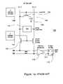
- FIG. 1( a )is a schematic diagram of a data sensing and capture circuit according to the prior art
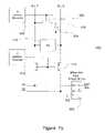
- FIG. 1( b )is a schematic diagram of a data sensing and capture circuit according to the present invention
- FIG. 2is a schematic diagram of a single input D type flip-flop
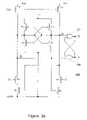
- FIG. 3( a )is a schematic diagram of a differential input flip-flop circuit according to an embodiment of the present invention.
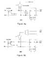
- FIG. 3( b )is a schematic diagram of a clock gating circuit according to the present invention.
- FIG. 4is a diagram of the timing waveforms for the circuit of FIG. 3(B) ;
- FIG. 5is a schematic diagram of a further embodiment of the present invention.
- FIGS. 6( a ) and 6 ( b )are schematic diagrams of further embodiments of the present invention.
- FIG. 1Athere is shown a schematic diagram of part of a data output circuit 100 for a semiconductor memory according to the prior art.
- the output circuitincludes memory cells 102 comprised of a storage capacitor 104 coupled to a bitline BLT via an access transistor 106 .
- the access transistors 106have their gates coupled along wordlines that are activated by signals generated by an X address decoder 108 .
- Bit line sense amplifiers 110are coupled between complementary pairs of bitlines.
- Columns of memory cells 102 or bitlinesare coupled to data bus lines DB and DB via respective column access devices 112 .
- the column access devices 112are normally activated by signals from an Y address decoder 114 .
- a differential input data bus sense amplifier 116the output of which drives a single input D-type flip-flop 118 , senses the data bus lines DB and DB .
- the flip-flop 118has its Q output coupled to a Read data output line.
- the data bus sense amplifiersenses the data in the lines, which is then latched by clocking the flip-flop 118 .
- FIG. 1Bthere is shown a data output circuit 150 according to an embodiment of the present invention.
- a data output circuit 150rather than having a separate data bus sense amplifier 116 and a single input D-type flip-flop 118 as shown in FIG. 1A , there is provided a single differential input D-type flip flop 300 having differential inputs D+ and D ⁇ coupled directly to the data bus lines DB and DB .
- the flip-flop 300reduces unnecessary Read operation delays and improves power consumption during idle(non-read) periods. A detailed description of the flip-flop 300 follows.
- FIG. 2there is shown a schematic diagram of a traditional D type flip-flop 118 of the type shown in FIG. 1A .
- the flip-flop circuit 118has a single D input, a clock input CLK, and a pair of complimentary outputs Q and Q .
- this D type flip-flop 118is normally connected to the output of the data bus sense amplifier 116 and has one of its outputs connected to the read data path as shown schematically in FIG. 1A .
- the disadvantages of this circuit arrangementare discussed in the background of the invention.
- the flip-flop 118has a data input circuit comprised of a pair of cross-coupled n-channel transistors N 4 and N 5 , the sources of which are coupled through an n-channel transistor N 3 to ground.
- the drains of the respective cross-coupled transistors N 4 and N 5are coupled to respective input transistors N 1 and N 2 which in-turn couple the transistors N 4 and N 5 through respective p-channel transistors P 1 and P 2 to the supply voltage Vcc.
- the D inputis coupled to the gate of transistor N 1 while an inverted version of the D input is coupled to the gate of transistor N 2 via an inverter I 1 . While this circuit 118 is suitable for a single input, it has to be modified for differential data inputs.
- the flip-flop 300adapted for differential data input, according to an embodiment of the present invention.
- the flip-flop 300also has a data input circuit comprised of a pair of cross-coupled n-channel transistors N 4 and N 5 , the sources of which are coupled through an n-channel transistor N 3 to ground.
- the drains of the respective cross-coupled transistors N 4 and N 5are coupled to respective input transistors N 1 and N 2 which in-turn couple the transistors N 4 and N 5 through respective p-channel transistors P 1 and P 2 to the supply voltage Vcc.
- a latch type amplifier circuitis coupled to nodes ID and ID formed around p-channel transistors P 3 , P 4 , n-channel transistors N 6 , N 7 and cross-coupled NAND gates 308 and 310 .
- the second differential input D ⁇is provided directly to the gate of transistor N 2 .
- the complimentary data inputsare now shown as D+ and D ⁇ coupled to respective gates of transistors N 1 and N 2 .
- transistor N 3was removed and a complementary version CLKN of the clock input CLK was added to provide ground supply voltage during the time that the clock input CLK is logic ‘1’; this is accomplished by connecting the CLKN signal to the drains of pull down transistors N 4 and N 5 .
- CLKNcomplementary version of the clock input CLK
- the clock inputallows gating of the differential flip flop 300 for disabling it when read operations are not being performed. This modification also limits negative impact on clock-to-read-data output timing of the memory.
- a clock gating circuit 382comprises a two input NOR gate having a gating clock GCLK input and an enable input ENN.
- the output of the NOR gateis coupled to the CLKN inputs of the differential input flip flops 300 (which as shown in FIG. 3A is provided to the drains of transistors N 4 and N 5 ) and an inverted version of the output is connected to the CLK inputs of the flip flops 300 (which as shown in FIG. 3A is provided to the gates of transistors P 1 and P 2 ).
- the clock gating circuit 382selectively enables the flip flops 300 to accept differential input data and provide single ended read data outputs RD 1 and RD 2 .
- FIG. 4there is shown the timing waveforms associated with the operation of a clock gating circuitry 382 and the differential input flip flops 300 .
- three illustrative periods of the GCLK clock signalcomprise a “read 0” followed by an “idle” followed by a “read 1 ” operations, although this sequence is not required in order to implement the invention.
- the active low enable signal ENN signalis low, thereby enabling the NOR gate in the clock gating circuit 382 .
- the output of the NOR gateWith the NOR gate enabled, on the subsequent falling edge of the GCLK, the output of the NOR gate generates the CLKN pulse and the output of the inverter of clock gating circuit 382 generates the CLK pulse.
- transistors P 1 and P 2 in FIG. 3AWith the CLK pulse being low, transistors P 1 and P 2 in FIG. 3A are turned on and precharge the ID and ID 0 signals both high while the input stage comprising transistors N 1 , N 2 , N 4 , N 5 is disabled since CLKN is high.
- the differential inputs D+ and D ⁇are sensed and latched by flip flop 300 on the falling edge of CLKN, generating Q and Q outputs.
- the “idle” cyclemaintains ENN high, thereby disabling the clock gating circuit 382 and maintaining the same outputs on Q and Q .
- the ENN signalis once again asserted thereby enabling the clock gating circuit 382 .
- the falling edge of the CLK signalprecharges both the ID and the ID signals high.
- the falling edge of the CLKN signalthen senses and latches the differential data which in turn generates the Q and Q outputs of the flip flop 300 . Accordingly, the differential input flip-flops 300 reduce unnecessary power consumption by gating the clock input to the differential flip-flop and disabling it when reading operations are not being performed.
- FIG. 5there is shown another embodiment of the differential input flip flop circuit 300 that supports limited dynamic power management without external clock gating circuitry or a complimentary clock input.
- a pair of P channel devicesis controlled by an enable signal and an additional transistor N 8 is connected to a transistor N 3 that is also driven by the enable signal.
- the CLKN signalis not used.
- FIGS. 6A and 6Bthere is shown a still further embodiment of the invention as applied to short bit line DRAM arrays.
- the differential input flip flops 300are coupled to the bit lines to directly sense and capture memory cell read out for voltage levels.
- This configurationis best suited for small memory arrays where layout rules allow the fitting of the flip flop circuits within the bitline pitch or having the flip flop circuits staggered to fit within the bitline pitch. This would allow for a very fast circuit implementation since all the control and timing circuits associated with the data bus sensing and latching would be omitted.
- FIG. 6Athe differential input flip flop 300 is shown connected in conjunction with a conventional bit line sense amplifier and in FIG.
- the differential input flip flop 300is shown as a replacement for a conventional bit line sense amplifier. It may be noted that in the configuration shown in FIG. 6B , the data captured by the circuit would have to be written back (either using the normal write operation circuitry or special purpose restoration circuitry) to restore memory cell voltage levels.
- the differential input flip flopis used in conjunction with a conventional sense amplifier as shown in FIG. 6A , the circuit allows read data to be captured prior to or in the process of restoration of full swing voltage levels on the bit line pair by the conventional sense amplifier.
- the inventioncan be applied to other situations where long pairs of wires are used to transmit data either differentially or dual rail within synchronous systems.
- Thismay include high performance synchronous SRAMs, other types of electronic memories with registered outputs, and long, heavily loaded differential or dual rail data buses within the datapaths of digital signal processors and microprocessors.
Landscapes
- Engineering & Computer Science (AREA)
- Microelectronics & Electronic Packaging (AREA)
- Computer Hardware Design (AREA)
- Dram (AREA)
- Static Random-Access Memory (AREA)
Abstract
Description
- (a) a differential input stage circuit for receiving respective ones of said differential data signals and having first and second output nodes;
- (b) a latch element having first and second complementary inputs coupled to receive signals from said respective first and second output nodes; and
- (c) a gating circuit for dynamically enabling and disabling a clock signal to said differential input stage in response to an enable signal, such that power consumption in said differential input stage is conserved.
Claims (5)
Applications Claiming Priority (3)
| Application Number | Priority Date | Filing Date | Title |
|---|---|---|---|
| CA2,313,948 | 2000-07-07 | ||
| CA002313948ACA2313948A1 (en) | 2000-07-07 | 2000-07-07 | Low delay, conditional differential data sense and capture scheme for a high speed dram |
| PCT/CA2000/000879WO2002005282A1 (en) | 2000-07-07 | 2000-07-31 | A method and apparatus for simultaneous differential data sensing and capture in a high speed memory |
Related Parent Applications (1)
| Application Number | Title | Priority Date | Filing Date |
|---|---|---|---|
| PCT/CA2000/000879ContinuationWO2002005282A1 (en) | 2000-07-07 | 2000-07-31 | A method and apparatus for simultaneous differential data sensing and capture in a high speed memory |
Publications (2)
| Publication Number | Publication Date |
|---|---|
| US20030156461A1 US20030156461A1 (en) | 2003-08-21 |
| US7269075B2true US7269075B2 (en) | 2007-09-11 |
Family
ID=4166719
Family Applications (1)
| Application Number | Title | Priority Date | Filing Date |
|---|---|---|---|
| US10/337,346Expired - LifetimeUS7269075B2 (en) | 2000-07-07 | 2003-01-07 | Method and apparatus for simultaneous differential data sensing and capture in a high speed memory |
Country Status (7)
| Country | Link |
|---|---|
| US (1) | US7269075B2 (en) |
| JP (1) | JP2004502268A (en) |
| KR (1) | KR100816939B1 (en) |
| CN (2) | CN101441888B (en) |
| AU (1) | AU2000264193A1 (en) |
| CA (1) | CA2313948A1 (en) |
| WO (1) | WO2002005282A1 (en) |
Cited By (1)
| Publication number | Priority date | Publication date | Assignee | Title |
|---|---|---|---|---|
| US20090109785A1 (en)* | 2007-10-31 | 2009-04-30 | Texas Instruments Incorporated | Memory having circuitry controlling the voltage differential between the word line and array supply voltage |
Families Citing this family (19)
| Publication number | Priority date | Publication date | Assignee | Title |
|---|---|---|---|---|
| WO2002005281A2 (en) | 2000-07-07 | 2002-01-17 | Mosaid Technologies Incorporated | A high speed dram architecture with uniform access latency |
| US7071737B2 (en)* | 2004-07-13 | 2006-07-04 | Kabushiki Kaisha Toshiba | Systems and methods for controlling timing in a circuit |
| KR100967386B1 (en)* | 2008-05-07 | 2010-07-05 | 주식회사 케이디파워 | Busbar fastening clips |
| KR200451968Y1 (en)* | 2008-07-14 | 2011-01-25 | 심상민 | Bus-bar connector |
| KR100956783B1 (en)* | 2008-10-14 | 2010-05-12 | 주식회사 하이닉스반도체 | Semiconductor memory device |
| US8283960B2 (en)* | 2009-04-27 | 2012-10-09 | Oracle America, Inc. | Minimal bubble voltage regulator |
| US8179165B2 (en)* | 2009-04-27 | 2012-05-15 | Oracle America, Inc. | Precision sampling circuit |
| US8242823B2 (en) | 2009-04-27 | 2012-08-14 | Oracle America, Inc. | Delay chain initialization |
| KR101111972B1 (en)* | 2009-12-04 | 2012-02-14 | 김계수 | Distribution Booth Bar |
| US9911470B2 (en)* | 2011-12-15 | 2018-03-06 | Nvidia Corporation | Fast-bypass memory circuit |
| US10141930B2 (en) | 2013-06-04 | 2018-11-27 | Nvidia Corporation | Three state latch |
| US9997232B2 (en)* | 2016-03-10 | 2018-06-12 | Micron Technology, Inc. | Processing in memory (PIM) capable memory device having sensing circuitry performing logic operations |
| US10395704B2 (en) | 2017-12-22 | 2019-08-27 | Micron Technology, Inc. | Apparatuses and methods for duty cycle error correction of clock signals |
| US10249354B1 (en) | 2018-02-23 | 2019-04-02 | Micron Technology, Inc. | Apparatuses and methods for duty cycle distortion correction of clocks |
| EP3803872A4 (en) | 2018-05-29 | 2022-03-09 | Micron Technology, Inc. | DEVICES AND METHODS FOR ADJUSTING A DUTY CYCLE ADJUSTER TO IMPROVE DUTY CYCLE |
| US11189334B2 (en) | 2018-11-21 | 2021-11-30 | Micron Technology, Inc. | Apparatuses and methods for a multi-bit duty cycle monitor |
| US10715127B2 (en) | 2018-11-21 | 2020-07-14 | Micron Technology, Inc. | Apparatuses and methods for using look-ahead duty cycle correction to determine duty cycle adjustment values while a semiconductor device remains in operation |
| CN112712833B (en)* | 2019-10-25 | 2024-10-01 | 长鑫存储技术(上海)有限公司 | Write operation circuit, semiconductor memory and write operation method |
| CN116092549B (en)* | 2023-01-16 | 2023-08-18 | 浙江力积存储科技有限公司 | Storage structure |
Citations (6)
| Publication number | Priority date | Publication date | Assignee | Title |
|---|---|---|---|---|
| US5297092A (en)* | 1992-06-03 | 1994-03-22 | Mips Computer Systems, Inc. | Sense amp for bit line sensing and data latching |
| US5452239A (en) | 1993-01-29 | 1995-09-19 | Quickturn Design Systems, Inc. | Method of removing gated clocks from the clock nets of a netlist for timing sensitive implementation of the netlist in a hardware emulation system |
| US5485430A (en)* | 1992-12-22 | 1996-01-16 | Sgs-Thomson Microelectronics, Inc. | Multiple clocked dynamic sense amplifier |
| US5959899A (en) | 1998-08-25 | 1999-09-28 | Mosel Vitelic Corporation | Semiconductor memory having single path data pipeline for CAS-latency |
| US5977798A (en) | 1997-02-28 | 1999-11-02 | Rambus Incorporated | Low-latency small-swing clocked receiver |
| US6201418B1 (en)* | 1998-08-13 | 2001-03-13 | Compaq Computer Corporation | Differential sense amplifier with reduced hold time |
Family Cites Families (7)
| Publication number | Priority date | Publication date | Assignee | Title |
|---|---|---|---|---|
| JPH08250997A (en)* | 1995-03-14 | 1996-09-27 | Fujitsu Ltd | Input circuit |
| JPH10327066A (en)* | 1997-05-27 | 1998-12-08 | Sony Corp | NMOS gate input type sense amplifier in transistor logic circuit |
| US5977789A (en)* | 1997-08-27 | 1999-11-02 | Intel Corporation | Fast-switching logic gate |
| JP3488612B2 (en)* | 1997-12-11 | 2004-01-19 | 株式会社東芝 | Sense amplifier circuit |
| JP4057125B2 (en)* | 1998-01-23 | 2008-03-05 | 株式会社ルネサステクノロジ | Semiconductor memory device |
| KR100304195B1 (en)* | 1998-09-18 | 2001-11-22 | 윤종용 | Synchronous Semiconductor Memory Device with External Clock Signal |
| JP3510507B2 (en)* | 1998-11-27 | 2004-03-29 | Necマイクロシステム株式会社 | Latch circuit |
- 2000
- 2000-07-07CACA002313948Apatent/CA2313948A1/ennot_activeAbandoned
- 2000-07-31CNCN2008100998703Apatent/CN101441888B/ennot_activeExpired - Lifetime
- 2000-07-31WOPCT/CA2000/000879patent/WO2002005282A1/enactiveApplication Filing
- 2000-07-31AUAU2000264193Apatent/AU2000264193A1/ennot_activeAbandoned
- 2000-07-31KRKR1020037000186Apatent/KR100816939B1/ennot_activeExpired - Lifetime
- 2000-07-31CNCN00819833Apatent/CN1454384A/enactivePending
- 2000-07-31JPJP2002508800Apatent/JP2004502268A/ennot_activeWithdrawn
- 2003
- 2003-01-07USUS10/337,346patent/US7269075B2/ennot_activeExpired - Lifetime
Patent Citations (6)
| Publication number | Priority date | Publication date | Assignee | Title |
|---|---|---|---|---|
| US5297092A (en)* | 1992-06-03 | 1994-03-22 | Mips Computer Systems, Inc. | Sense amp for bit line sensing and data latching |
| US5485430A (en)* | 1992-12-22 | 1996-01-16 | Sgs-Thomson Microelectronics, Inc. | Multiple clocked dynamic sense amplifier |
| US5452239A (en) | 1993-01-29 | 1995-09-19 | Quickturn Design Systems, Inc. | Method of removing gated clocks from the clock nets of a netlist for timing sensitive implementation of the netlist in a hardware emulation system |
| US5977798A (en) | 1997-02-28 | 1999-11-02 | Rambus Incorporated | Low-latency small-swing clocked receiver |
| US6201418B1 (en)* | 1998-08-13 | 2001-03-13 | Compaq Computer Corporation | Differential sense amplifier with reduced hold time |
| US5959899A (en) | 1998-08-25 | 1999-09-28 | Mosel Vitelic Corporation | Semiconductor memory having single path data pipeline for CAS-latency |
Cited By (3)
| Publication number | Priority date | Publication date | Assignee | Title |
|---|---|---|---|---|
| US20090109785A1 (en)* | 2007-10-31 | 2009-04-30 | Texas Instruments Incorporated | Memory having circuitry controlling the voltage differential between the word line and array supply voltage |
| WO2009058991A1 (en)* | 2007-10-31 | 2009-05-07 | Texas Instruments Incorporated | Memory having circuitry controlling the voltage differential between the word line and array supply voltage |
| US7907456B2 (en) | 2007-10-31 | 2011-03-15 | Texas Instruments Incorporated | Memory having circuitry controlling the voltage differential between the word line and array supply voltage |
Also Published As
| Publication number | Publication date |
|---|---|
| KR100816939B1 (en) | 2008-03-26 |
| JP2004502268A (en) | 2004-01-22 |
| AU2000264193A1 (en) | 2002-01-21 |
| KR20030045771A (en) | 2003-06-11 |
| CN1454384A (en) | 2003-11-05 |
| WO2002005282A1 (en) | 2002-01-17 |
| CN101441888B (en) | 2011-10-19 |
| US20030156461A1 (en) | 2003-08-21 |
| CN101441888A (en) | 2009-05-27 |
| CA2313948A1 (en) | 2002-01-07 |
Similar Documents
| Publication | Publication Date | Title |
|---|---|---|
| US7269075B2 (en) | Method and apparatus for simultaneous differential data sensing and capture in a high speed memory | |
| US6181634B1 (en) | Multiple-port semiconductor memory device | |
| KR0164199B1 (en) | Semiconductor memory | |
| KR910008101B1 (en) | Feedback type data output circuit of semiconductor memory device | |
| JPH0546040B2 (en) | ||
| JPH02201797A (en) | semiconductor memory device | |
| JPH0253879B2 (en) | ||
| US8218385B2 (en) | Current mode data sensing and propagation using voltage amplifier | |
| JPH03283186A (en) | Dynamic type semiconductor memory device | |
| US6240043B1 (en) | SDRAM with a maskable input | |
| US6356487B1 (en) | Memory device having data path containing dual mode flip-flop used for normal operation and for internal testing | |
| US5856949A (en) | Current sense amplifier for RAMs | |
| KR20010048993A (en) | Method of prefetch and restore in semiconductor memory device and circuit thereof | |
| US6633503B2 (en) | Voltage differential sensing circuit and methods of using same | |
| KR100299468B1 (en) | Power saving synchronization circuit and semiconductor storage device including the same | |
| KR950010628B1 (en) | Column Decoder Enable Signal Generation Circuit of Semiconductor Device | |
| US6434079B2 (en) | Semiconductor memory device for distributing load of input and output lines | |
| JP3105318B2 (en) | Semiconductor integrated circuit device | |
| JPH08138377A (en) | Semiconductor memory device | |
| US10311941B1 (en) | Apparatuses and methods for input signal receiver circuits | |
| US6026496A (en) | Method and apparatus for generating a pulse | |
| JPH01196790A (en) | Semiconductor memory device | |
| CA2414248A1 (en) | A method and apparatus for simultaneous differential data sensing and capture in a high speed memory | |
| KR100337205B1 (en) | Data sense amplifier driver | |
| JP3082229B2 (en) | Memory device |
Legal Events
| Date | Code | Title | Description |
|---|---|---|---|
| AS | Assignment | Owner name:MOSAID TECHNOLOGIES INCORPORATED, CANADA Free format text:ASSIGNMENT OF ASSIGNORS INTEREST;ASSIGNOR:DEMONE, PAUL;REEL/FRAME:017214/0164 Effective date:20051212 | |
| STCF | Information on status: patent grant | Free format text:PATENTED CASE | |
| AS | Assignment | Owner name:MOSAID TECHNOLOGIES INCORPORATED, CANADA Free format text:CHANGE OF ADDRESS OF ASSIGNEE;ASSIGNOR:MOSAID TECHNOLOGIES INCORPORATED;REEL/FRAME:022542/0876 Effective date:20090209 Owner name:MOSAID TECHNOLOGIES INCORPORATED,CANADA Free format text:CHANGE OF ADDRESS OF ASSIGNEE;ASSIGNOR:MOSAID TECHNOLOGIES INCORPORATED;REEL/FRAME:022542/0876 Effective date:20090209 | |
| FEPP | Fee payment procedure | Free format text:PAYOR NUMBER ASSIGNED (ORIGINAL EVENT CODE: ASPN); ENTITY STATUS OF PATENT OWNER: LARGE ENTITY | |
| FPAY | Fee payment | Year of fee payment:4 | |
| AS | Assignment | Owner name:ROYAL BANK OF CANADA, CANADA Free format text:U.S. INTELLECTUAL PROPERTY SECURITY AGREEMENT (FOR NON-U.S. GRANTORS) - SHORT FORM;ASSIGNORS:658276 N.B. LTD.;658868 N.B. INC.;MOSAID TECHNOLOGIES INCORPORATED;REEL/FRAME:027512/0196 Effective date:20111223 | |
| AS | Assignment | Owner name:CONVERSANT INTELLECTUAL PROPERTY MANAGEMENT INC., Free format text:CHANGE OF NAME;ASSIGNOR:MOSAID TECHNOLOGIES INCORPORATED;REEL/FRAME:032439/0638 Effective date:20140101 | |
| AS | Assignment | Owner name:CONVERSANT INTELLECTUAL PROPERTY MANAGEMENT INC., Free format text:RELEASE OF SECURITY INTEREST;ASSIGNOR:ROYAL BANK OF CANADA;REEL/FRAME:033484/0344 Effective date:20140611 Owner name:CONVERSANT IP N.B. 276 INC., CANADA Free format text:RELEASE OF SECURITY INTEREST;ASSIGNOR:ROYAL BANK OF CANADA;REEL/FRAME:033484/0344 Effective date:20140611 Owner name:CONVERSANT IP N.B. 868 INC., CANADA Free format text:RELEASE OF SECURITY INTEREST;ASSIGNOR:ROYAL BANK OF CANADA;REEL/FRAME:033484/0344 Effective date:20140611 | |
| AS | Assignment | Owner name:CONVERSANT INTELLECTUAL PROPERTY MANAGEMENT INC., CANADA Free format text:CHANGE OF ADDRESS;ASSIGNOR:CONVERSANT INTELLECTUAL PROPERTY MANAGEMENT INC.;REEL/FRAME:033678/0096 Effective date:20140820 Owner name:CONVERSANT INTELLECTUAL PROPERTY MANAGEMENT INC., Free format text:CHANGE OF ADDRESS;ASSIGNOR:CONVERSANT INTELLECTUAL PROPERTY MANAGEMENT INC.;REEL/FRAME:033678/0096 Effective date:20140820 | |
| AS | Assignment | Owner name:CPPIB CREDIT INVESTMENTS INC., AS LENDER, CANADA Free format text:U.S. PATENT SECURITY AGREEMENT (FOR NON-U.S. GRANTORS);ASSIGNOR:CONVERSANT INTELLECTUAL PROPERTY MANAGEMENT INC.;REEL/FRAME:033706/0367 Effective date:20140611 Owner name:ROYAL BANK OF CANADA, AS LENDER, CANADA Free format text:U.S. PATENT SECURITY AGREEMENT (FOR NON-U.S. GRANTORS);ASSIGNOR:CONVERSANT INTELLECTUAL PROPERTY MANAGEMENT INC.;REEL/FRAME:033706/0367 Effective date:20140611 | |
| FPAY | Fee payment | Year of fee payment:8 | |
| AS | Assignment | Owner name:CPPIB CREDIT INVESTMENTS, INC., CANADA Free format text:AMENDED AND RESTATED U.S. PATENT SECURITY AGREEMENT (FOR NON-U.S. GRANTORS);ASSIGNOR:CONVERSANT INTELLECTUAL PROPERTY MANAGEMENT INC.;REEL/FRAME:046900/0136 Effective date:20180731 | |
| AS | Assignment | Owner name:CONVERSANT INTELLECTUAL PROPERTY MANAGEMENT INC., CANADA Free format text:RELEASE OF U.S. PATENT AGREEMENT (FOR NON-U.S. GRANTORS);ASSIGNOR:ROYAL BANK OF CANADA, AS LENDER;REEL/FRAME:047645/0424 Effective date:20180731 Owner name:CONVERSANT INTELLECTUAL PROPERTY MANAGEMENT INC., Free format text:RELEASE OF U.S. PATENT AGREEMENT (FOR NON-U.S. GRANTORS);ASSIGNOR:ROYAL BANK OF CANADA, AS LENDER;REEL/FRAME:047645/0424 Effective date:20180731 | |
| MAFP | Maintenance fee payment | Free format text:PAYMENT OF MAINTENANCE FEE, 12TH YEAR, LARGE ENTITY (ORIGINAL EVENT CODE: M1553); ENTITY STATUS OF PATENT OWNER: LARGE ENTITY Year of fee payment:12 | |
| AS | Assignment | Owner name:CONVERSANT INTELLECTUAL PROPERTY MANAGEMENT INC., CANADA Free format text:RELEASE BY SECURED PARTY;ASSIGNOR:CPPIB CREDIT INVESTMENTS INC.;REEL/FRAME:054278/0333 Effective date:20201028 |