US7269044B2 - Method and apparatus for accessing a memory array - Google Patents
Method and apparatus for accessing a memory arrayDownload PDFInfo
- Publication number
- US7269044B2 US7269044B2US11/111,838US11183805AUS7269044B2US 7269044 B2US7269044 B2US 7269044B2US 11183805 AUS11183805 AUS 11183805AUS 7269044 B2US7269044 B2US 7269044B2
- Authority
- US
- United States
- Prior art keywords
- line
- transistor
- transistors
- electrode
- gate
- Prior art date
- Legal status (The legal status is an assumption and is not a legal conclusion. Google has not performed a legal analysis and makes no representation as to the accuracy of the status listed.)
- Expired - Lifetime, expires
Links
Images


Classifications
- G—PHYSICS
- G11—INFORMATION STORAGE
- G11C—STATIC STORES
- G11C13/00—Digital stores characterised by the use of storage elements not covered by groups G11C11/00, G11C23/00, or G11C25/00
- G11C13/0002—Digital stores characterised by the use of storage elements not covered by groups G11C11/00, G11C23/00, or G11C25/00 using resistive RAM [RRAM] elements
- G11C13/0009—RRAM elements whose operation depends upon chemical change
- G11C13/0011—RRAM elements whose operation depends upon chemical change comprising conductive bridging RAM [CBRAM] or programming metallization cells [PMCs]
- G—PHYSICS
- G11—INFORMATION STORAGE
- G11C—STATIC STORES
- G11C2213/00—Indexing scheme relating to G11C13/00 for features not covered by this group
- G11C2213/70—Resistive array aspects
- G11C2213/79—Array wherein the access device being a transistor
Definitions
- the inventionrelates to the field of random access memory (RAM) devices formed using a resistance variable material.
- Resistance variable memory elementswhich include Programmable Conductive Random Access Memory (PCRAM) elements, have been investigated for suitability as semi-volatile and non-volatile random access memory devices.
- PCRAMProgrammable Conductive Random Access Memory
- a typical resistance variable memory element formed using a chalcogenide glass backboneis disclosed in U.S. Pat. No. 6,348,365 to Moore and Gilton.
- a conductive materialsuch as silver
- the resistance of the chalcogenide glasscan be programmed to stable higher resistance and lower resistance states.
- An unprogrammed chalcogenide variable resistance elementis normally in a higher resistance state.
- a write operationprograms the element to a lower resistance state by applying a voltage potential across the chalcogenide glass and forming a conductive pathway. The element may then be read by applying a voltage pulse of a lesser magnitude than required to program it; the resistance across the memory device is then sensed as higher or lower to define two logic states.
- the programmed lower resistance state of a chalcogenide variable resistance elementcan remain intact for a considerable period of time, typically ranging from hours to weeks, after the voltage potentials are removed.
- the elementcan be returned to its higher resistance state by applying a reverse voltage potential of about the same order of magnitude as used to write the device to the lower resistance state. Again, the higher resistance state is maintained in a semi- or non-volatile manner once the voltage potential is removed.
- such an elementcan function as a variable resistance non-volatile memory having at least two resistance states, which can define two respective logic states, i.e., at least a bit of data.
- a plurality of resistance variable memory devicescan be included in a memory array. In doing so, it is desirable to provide a greater number of memory elements within a particular area.
- Exemplary embodiments of the inventionprovide a resistance variable memory device including first and second memory elements and methods for operating the same.
- the first and second memory elementseach have first and second electrodes.
- the first electrode of the first and second memory elementsis a common first electrode and is located below the second electrodes.
- a first lineis connected to the second electrode of the first memory element and a second line connected to the second electrode of the second memory element.
- the first and second linesare switchably connected to a third line for applying a voltage to the second electrodes.
- FIG. 1is a diagram of a memory device according to an exemplary embodiment of the invention.
- FIG. 2is a diagram of a memory device according to another exemplary embodiment of the invention.
- FIG. 3Ais a top plan view of a portion of a memory array according to an exemplary embodiment of the invention.
- FIG. 3Bis a cross sectional view of the memory array of FIG. 3A along liner 3 A- 3 A′ and according to an exemplary embodiment of the invention
- FIG. 3Cis a cross sectional view of the memory array of FIG. 3A along liner 3 A- 3 A′ and according to another exemplary embodiment of the invention.
- FIG. 4is a block diagram of a system including a memory device according to an exemplary embodiment of the invention.
- substrateused in the following description may include any supporting structure including, but not limited to, a semiconductor substrate that has an exposed substrate surface.
- a semiconductor substrateshould be understood to include silicon-on-insulator (SOI), silicon-on-sapphire (SOS), doped and undoped semiconductors, epitaxial layers of silicon supported by a base semiconductor foundation, and other semiconductor structures.
- SOIsilicon-on-insulator
- SOSsilicon-on-sapphire
- doped and undoped semiconductorssilicon-on-insulator
- epitaxial layers of silicon supported by a base semiconductor foundationand other semiconductor structures.
- the substrateneed not be semiconductor-based, but may be any support structure suitable for supporting an integrated circuit, including, but not limited to, metals, alloys, glasses, polymers, ceramics, and any other supportive materials as is known in the art.
- a substratecan include layers and structures over a semiconductor substrate, wafer, or other material, such as conductive lines and/or insulating layers.
- resistance variable memory elementis intended to include any memory element, including programmable conductor memory elements, semi-volatile memory elements, and non-volatile memory elements, which exhibit a resistance change in response to applied programming voltages.
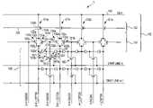
- FIG. 1depicts a portion of a memory device 1 according to an exemplary embodiment of the invention.
- the memory device 1includes a memory array 100 and circuitry 102 for accessing the memory array 100 .
- the array 100includes a plurality of memory units 101 .
- Each memory unit 101includes a plurality of memory elements 101 a , 101 b .
- each memory unit 101includes two memory elements, 101 a , 101 b , each for storing one bit of data, e.g., a logic 1 or 0.
- the memory elements 101 a , 101 bare resistance variable memory elements arranged in columns and rows.
- the anodes (first electrodes) 212 of the elements 101 a , 101 bare coupled to a source/drain region 161 a of a transistor 160 .
- a second source/drain region 161 b of the transistor 160is coupled to digit line n and the gate 161 c of transistor 160 is coupled to a word line, e.g., word line n+2 as shown in FIG. 1 .
- the memory elements 101 a , 101 b of a single memory unit 101share a common first electrode 212 . Such an embodiment is described in more detail below in connection with FIGS. 3A-3C .
- the cathode (second electrode) 251 of memory element 101 ais coupled to a first select line, e.g., select line n+2, while the second electrode 251 of memory element 101 b is coupled to a second select line, e.g., select line n+3. Accordingly, a single memory unit 101 is addressable by two different select lines.
- first electrodes 212are shown as anodes and second electrodes 251 are shown as cathodes, it should be understood that, alternatively, first electrodes 212 can be cathodes and second electrodes 251 can be anodes.
- FIG. 1also depicts circuitry 102 for accessing particular memory elements 101 a , 101 b of the memory units 101 .
- a select linefor example, select line n+2 connects to the source/drain region 132 b of two select transistors, 131 a , 131 b .
- the source/drain regions 132 a of the select transistors 131 a , 131 bare coupled to each other, and the source/drain regions 132 b of the select transistors 131 a , 131 b are coupled to each other.
- the gate 132 c of the select transistor 131 ais coupled to word line n+2.
- Gate 132 c of select transistor 131 cis connected to word line n+1.
- the gates 161 c of the transistors 160are also associated with respective word lines.
- the gate 132 c of transistor 131 ais connected to word line n+2, which in turn is connected to the gate 161 c of a transistor 160 ; while the gate 132 c of transistor 131 b is connected to word line n+1, which is connected to the gate 161 c of the transistor 160 associated with the memory unit 101 .
- select line n+3connects to the source/drain region 132 b of two select transistors, 131 c , 131 d .
- First source/drain regions 132 a of the select transistors 131 c , 131 dare coupled to each other, and second source/drain regions 132 b of the select transistors 131 c , 131 d are coupled to each other.
- the gate 132 c of transistor 131 cis connected to word line n+3, while the gate 132 c of transistor 131 d is connected to word line n+2.
- the circuitry 102also includes a plurality of A/B transistors 121 .
- the A/B transistorsalternate in a left right direction of the FIG. 1 array 100 between p-channel 121 p and n-channel 121 n transistors.
- the source/drain regions 132 a of select transistors 131 a , 131 bare connected to a source/drain region 122 a of an n-channel A/B transistor 121 n ; source/drain regions 132 a of select transistors 131 c , 131 d are connected to a source/drain region 122 a of a p-channel A/B transistor 121 p .
- the A/B select line 125is driven high to operate gates 122 c of the n-channel A/B transistors 121 n and is driven low to operate gates 122 c of the p-channel A/B transistors 121 p.
- the gates 122 c of the A/B transistors 121are connected to an A/B select line 125 .
- the source drain regions 122 b of the A/B transistors 121are connected to a common Cpin line 140 .
- the Cpin line 140is used to apply voltage and current to the memory element 101 a , 101 b second electrodes 251 for read and programming operations.
- the memory elements 101 a , 101 bare initially in a high resistance state and can be programmed to a low resistance state. Further, the memory elements 101 a , 101 b can be reprogrammed (erased) to a high resistance state. Each resistance state represents one of a logic 1 or 0 and can be read from the memory elements 101 a , 101 b .
- Write, read and eraseare performed by controlling the application of voltages across the memory elements 101 a , 101 b using the word lines (e.g., word line n+2); select lines(e.g., select lines n+2, n+3); paired transistors 131 a , 131 b , 131 c , 131 d ; A/B transistors 121 n , 121 p ; transistors 160 ; and digit lines (e.g., digit line n).
- word linese.g., word line n+2
- select linese.g., select lines n+2, n+3
- paired transistors 131 a , 131 b , 131 c , 131 dpaired transistors 131 a , 131 b , 131 c , 131 d ; A/B transistors 121 n , 121 p ; transistors 160 ; and digit lines (e.g., digit
- the voltage on Cpin line 140is applied to the element 101 a or 101 b .
- a voltage from Cpin line 140is applied to the second electrode 251 of memory element 101 a .
- the A/B select line 125is driven high to activate the gate 122 c of the A/B transistor 121 n .
- a voltageis applied to word line n+2 to activate the gate 132 c of select transistor 131 a .
- a currentcan flow from Cpin line 140 to select line n+2 to the second electrode 251 of memory element 101 a .
- the A/B select line 125is driven low to activate the gate 122 c of the A/B transistor 121 p .
- a voltageis applied to the word line n+2 to activate the gate 132 c of select transistor 131 d .
- a currentcan flow from Cpin line 140 to select line n+3 to the memory element 101 b 's second electrode 251 .
- a voltageis applied to digit line n.
- the voltage value applied to word line n+2 relative to the voltage applied to digit line n and supplied by Cpin line 140determines what operation is performed on the memory elements 101 a , 101 b .
- Exemplary voltages for read and write operationsare described in U.S. Pat. No. 6,791,885, assigned to Micron Technology, Inc, which is incorporated herein by reference. It should be appreciated that other voltages can be employed to perform read and write operations.
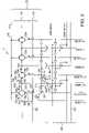
- FIG. 2illustrates a memory device 2 according to another exemplary embodiment according to the invention.
- the embodiment illustrated in FIG. 2is similar to that of FIG. 1 , but with the below noted exceptions.
- the source/drain regions 132 a of select transistors 131 a , 131 b , 131 c , 131 dare connected to Cpin line 140 .
- the source/drain regions 132 b of the select transistors 131 a , 131 bare connected to a source/drain region 122 b of an n-channel A/B transistor 121 n ; the source/drain regions 132 b of select transistors 131 c , 131 d are connected to a source/drain region 122 b of a p-channel A/B transistor 121 p .
- the source/drain region 122 a of the A/B transistor 121 nis connected to select line n+2; and the source drain region 122 a of A/B transistor 121 p is connected to select line n+3.
- Second electrodes 251 of the elements 101 a , 101 bcan be accessed for read and write operations as described above in connection with FIG. 1 . That is, to read or write, for example memory element 101 a , the A/B select line 125 is driven high to activate the gate 122 c of the A/B transistor 121 n . Additionally, a voltage is applied to word line n+2 to activate the gate 132 c of select transistor 131 a . Thereby, a current can flow from Cpin line 140 to select line n+2 and to the second electrode 251 of memory element 101 a .
- the A/B select line 125is driven low to activate the gate 122 c of the A/B transistor 121 p .
- a voltageis applied to the word line n+2 to activate the gate 132 c of select transistor 131 d .
- a currentcan flow from Cpin line 140 to select line n+3 to the memory element 101 b 's second electrode 251 .
- a voltageis applied to digit line n.
- the voltage value applied to word line n+2 relative to the voltage applied to digit line n and supplied by Cpin line 140determines what operation is performed on the memory elements 101 a , 101 b.
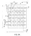
- FIG. 3Adepicts a top view of the memory array 100 according to either exemplary embodiment of the invention.
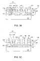
- FIG. 3Billustrates a portion of the memory array 100 of FIG. 3A along line 3 A- 3 A′ and according to one embodiment.
- FIG. 3Cillustrates a portion of the memory array 100 of FIG. 3A along line 3 A- 3 A′ and according to another embodiment.
- the array 100is supported by a substrate 210 .
- This electrode 212is preferably tungsten (W).
- An insulating layer 214is between the first electrodes 212 and can be, for example, silicon nitride (Si 3 N 4 ), a low dielectric constant material, an insulating glass, or an insulating polymer, but is not limited to such materials.
- a memory stack 240 of layersis formed over the first electrodes 212 .
- the stack memory 240includes one or more layers of resistance variable material.
- the stack 240can also include one or more layers of other materials, e.g., metal layers.
- the memory cell stack 240includes, for example, a chalcogenide material layer 241 (e.g., a chalcogenide glass, such as germanium selenide), a metal-chalcogenide layer 242 (e.g., tin selenide or silver selenide), and a metal layer 243 (e.g., silver).
- a chalcogenide material layer 241e.g., a chalcogenide glass, such as germanium selenide
- a metal-chalcogenide layer 242e.g., tin selenide or silver selenide
- a metal layer 243e.g., silver
- the stack 240can further include a second layer of chalcogenide material (not shown) over the metal layer 243 .
- the second layer of chalcogenide materialcan be the same material as the chalcogenide material layer 241 or a different material.
- the chalcogenide material layer 241is, e.g., germanium selenide (Ge x Se 100-x ).
- the germanium selenidemay be within a stoichiometric range of about Ge 33 Se 67 to about Ge 60 Se 40 .
- the chalcogenide material layer 241may be between about 100 ⁇ and about 1000 ⁇ thick, e.g., about 300 ⁇ thick.
- Layer 241need not be a single layer, but may also be comprised of multiple chalcogenide sub-layers having the same or different stoichiometries.
- the chalcogenide material layer 241is in electrical contact with the underlying electrodes 212 .
- chalcogenide material layer 241Over the chalcogenide material layer 241 is an optional layer of metal-chalcogenide 242 , for example tin selenide.
- metal-chalcogenide 242for example tin selenide.
- Other metal chalcogenide materialsmay also be used, such as silver-chalcogenide, for example silver selenide. It is also possible that other chalcogenide materials may be substituted for selenium, such as sulfur, oxygen, or tellurium.
- the tin-chalcogenide layer 242may be about 100 ⁇ to about 400 ⁇ thick; however, its thickness depends, in part, on the thickness of the underlying chalcogenide material layer 241 .
- the ratio of the thickness of the tin-chalcogenide layer 242 to that of the underlying chalcogenide material layer 241should be between about 5:1 and about 1:3.
- An optional metal layer 243is provided over the metal-chalcogenide layer 242 , with silver (Ag) being the exemplary metal. Desirably, this metal layer 243 is between about 300 ⁇ and about 500 ⁇ thick. Over the metal layer 243 are second electrodes 251 .
- the second electrodes 251can be formed of the same material as the first electrodes 212 , but is not required to be so. In the exemplary embodiment shown in FIGS. 3A-3C , the second electrodes 251 are preferably tungsten (W).
- all layers 241 , 242 , 243 of the memory stack 240are blanket layers and are continuously shared by all memory elements 101 a , 101 b of the array 100 .
- at least a portion of the stack 240is patterned to form element stacks 202 .
- Each element stack 202corresponds to a memory element 101 a , 101 b .
- FIG. 3Ball layers 241 , 242 , 243 of the memory stack 240 are blanket layers and are continuously shared by all memory elements 101 a , 101 b of the array 100 .
- at least a portion of the stack 240is patterned to form element stacks 202 .
- Each element stack 202corresponds to a memory element 101 a , 101 b .
- chalcogenide material layer 241is a blanket layer and is continuously shared by all memory elements 101 a ′, 101 b ′ of the array 100 , and tin-chalcogenide layer 242 and metal layer 243 are patterned.
- the layers 242 , 243are patterned similarly to the second electrodes 251 , as shown in FIG. 3C . While FIG. 3C shows only layers 242 , 243 patterned, layer 241 could also be patterned.
- the embodiment shown in FIG. 3Ccan be formed as described in application Ser. No. 11/111,917, filed Apr. 22, 2005 assigned to Micron Technology, Inc. and incorporated herein by reference.
- the second electrodes 251are formed as lines along the x direction.
- the first electrodes 212have a pitch 208 , which, for example, is the distance in the y direction from about the center of a first electrode 212 b in a first row to about the center of a first electrode 212 c in a neighboring row.
- the second electrodes 251have a pitch 209 , which is approximately the same as the pitch 208 of the first electrodes 212 .
- the second electrodes 251are off set by approximately one half pitch 208 (or 209 ) from the first electrodes 212 . Accordingly, as shown in FIGS. 3A-3C , each first electrode 212 underlies a region 260 between two second electrodes 251 .
- each first electrode 212underlies a portion of two adjacent second electrodes 251 .
- each first electrode 212 of word row nunderlies a portion of the two adjacent second electrodes 251 .
- stack 240is shown including layers 241 , 242 , 243 , it should be appreciated that one or more of layers 241 , 242 , 243 may be excluded and other layers may be included.
- Non limiting examples of materials and layers that can be included in stack 240 and materials for electrodes 212 , 251are discussed in various patents and patent applications assigned to Micron Technology, Inc., including, but not limited to the following: U.S. patent application Ser. No. 10/765,393; U.S. patent application Ser. No. 09/853,233; U.S. patent application Ser. No. 10/022,722; U.S. patent application Ser. No. 10/663,741; U.S. patent application Ser. No.
- the array 100includes memory elements 101 a , 101 b , each for storing one bit of data, i.e., a logic 1 or 0. Since each first electrode 212 underlies two second electrodes 251 , each first electrode 212 is associated with two memory elements 101 a , 101 b . Accordingly the bit density of the array 100 can be increased over prior art arrays that have a single first electrode associated with a single second electrode.
- applying a conditioning voltagecomprises applying a potential across the memory elements 101 a , 101 b such that material from the tin-chalcogenide layer 242 is incorporated into the chalcogenide material layer 241 , thereby forming a conducting channel through the layer 241 . Movement of ions from the layer 242 into or out of that conducting channel during subsequent programming forms a conductive pathway 221 a , 221 b , which causes a detectible resistance change across the memory elements 201 a , 201 b , respectively.
- FIG. 4illustrates a processor system 400 which includes a memory circuit 448 , e.g., a memory device 1 ( FIG. 1 ), which employs a memory array 100 and circuitry 102 according to the invention.
- the memory circuit 448could instead include the memory device 2 ( FIG. 2 ).
- the processor system 400which can be, for example, a computer system, generally comprises a central processing unit (CPU) 444 , such as a microprocessor, a digital signal processor, or other programmable digital logic devices, which communicates with an input/output (I/O) device 446 over a bus 452 .
- the memory circuit 448communicates with the CPU 444 over bus 452 typically through a memory controller.
- the processor system 400may include peripheral devices such as a floppy disk drive 454 and a compact disc (CD) ROM drive 456 , which also communicate with CPU 444 over the bus 452 .
- Memory circuit 448is preferably constructed as an integrated circuit, which includes a memory device 1 . If desired, the memory circuit 448 may be combined with the processor, for example CPU 444 , in a single integrated circuit.
Landscapes
- Semiconductor Memories (AREA)
Abstract
Description
Claims (38)
Priority Applications (1)
| Application Number | Priority Date | Filing Date | Title |
|---|---|---|---|
| US11/111,838US7269044B2 (en) | 2005-04-22 | 2005-04-22 | Method and apparatus for accessing a memory array |
Applications Claiming Priority (1)
| Application Number | Priority Date | Filing Date | Title |
|---|---|---|---|
| US11/111,838US7269044B2 (en) | 2005-04-22 | 2005-04-22 | Method and apparatus for accessing a memory array |
Publications (2)
| Publication Number | Publication Date |
|---|---|
| US20060239058A1 US20060239058A1 (en) | 2006-10-26 |
| US7269044B2true US7269044B2 (en) | 2007-09-11 |
Family
ID=37186671
Family Applications (1)
| Application Number | Title | Priority Date | Filing Date |
|---|---|---|---|
| US11/111,838Expired - LifetimeUS7269044B2 (en) | 2005-04-22 | 2005-04-22 | Method and apparatus for accessing a memory array |
Country Status (1)
| Country | Link |
|---|---|
| US (1) | US7269044B2 (en) |
Cited By (1)
| Publication number | Priority date | Publication date | Assignee | Title |
|---|---|---|---|---|
| US7825479B2 (en) | 2008-08-06 | 2010-11-02 | International Business Machines Corporation | Electrical antifuse having a multi-thickness dielectric layer |
Families Citing this family (1)
| Publication number | Priority date | Publication date | Assignee | Title |
|---|---|---|---|---|
| US7961507B2 (en)* | 2008-03-11 | 2011-06-14 | Micron Technology, Inc. | Non-volatile memory with resistive access component |
Citations (189)
| Publication number | Priority date | Publication date | Assignee | Title |
|---|---|---|---|---|
| US3271591A (en) | 1963-09-20 | 1966-09-06 | Energy Conversion Devices Inc | Symmetrical current controlling device |
| US3622319A (en) | 1966-10-20 | 1971-11-23 | Western Electric Co | Nonreflecting photomasks and methods of making same |
| US3743847A (en) | 1971-06-01 | 1973-07-03 | Motorola Inc | Amorphous silicon film as a uv filter |
| US3961314A (en) | 1974-03-05 | 1976-06-01 | Energy Conversion Devices, Inc. | Structure and method for producing an image |
| US3966317A (en) | 1974-04-08 | 1976-06-29 | Energy Conversion Devices, Inc. | Dry process production of archival microform records from hard copy |
| US3983542A (en) | 1970-08-13 | 1976-09-28 | Energy Conversion Devices, Inc. | Method and apparatus for recording information |
| US4177474A (en) | 1977-05-18 | 1979-12-04 | Energy Conversion Devices, Inc. | High temperature amorphous semiconductor member and method of making the same |
| US4267261A (en) | 1971-07-15 | 1981-05-12 | Energy Conversion Devices, Inc. | Method for full format imaging |
| US4269935A (en) | 1979-07-13 | 1981-05-26 | Ionomet Company, Inc. | Process of doping silver image in chalcogenide layer |
| US4312938A (en) | 1979-07-06 | 1982-01-26 | Drexler Technology Corporation | Method for making a broadband reflective laser recording and data storage medium with absorptive underlayer |
| US4316946A (en) | 1979-12-03 | 1982-02-23 | Ionomet Company, Inc. | Surface sensitized chalcogenide product and process for making and using the same |
| US4320191A (en) | 1978-11-07 | 1982-03-16 | Nippon Telegraph & Telephone Public Corporation | Pattern-forming process |
| US4405710A (en) | 1981-06-22 | 1983-09-20 | Cornell Research Foundation, Inc. | Ion beam exposure of (g-Gex -Se1-x) inorganic resists |
| US4419421A (en) | 1979-01-15 | 1983-12-06 | Max-Planck-Gesellschaft Zur Forderung Der Wissenschaften E.V. | Ion conductor material |
| US4499557A (en) | 1980-10-28 | 1985-02-12 | Energy Conversion Devices, Inc. | Programmable cell for use in programmable electronic arrays |
| US4597162A (en) | 1983-01-18 | 1986-07-01 | Energy Conversion Devices, Inc. | Method for making, parallel preprogramming or field programming of electronic matrix arrays |
| US4608296A (en) | 1983-12-06 | 1986-08-26 | Energy Conversion Devices, Inc. | Superconducting films and devices exhibiting AC to DC conversion |
| US4637895A (en) | 1985-04-01 | 1987-01-20 | Energy Conversion Devices, Inc. | Gas mixtures for the vapor deposition of semiconductor material |
| US4646266A (en) | 1984-09-28 | 1987-02-24 | Energy Conversion Devices, Inc. | Programmable semiconductor structures and methods for using the same |
| US4664939A (en) | 1985-04-01 | 1987-05-12 | Energy Conversion Devices, Inc. | Vertical semiconductor processor |
| US4668968A (en) | 1984-05-14 | 1987-05-26 | Energy Conversion Devices, Inc. | Integrated circuit compatible thin film field effect transistor and method of making same |
| US4670763A (en) | 1984-05-14 | 1987-06-02 | Energy Conversion Devices, Inc. | Thin film field effect transistor |
| US4671618A (en) | 1986-05-22 | 1987-06-09 | Wu Bao Gang | Liquid crystalline-plastic material having submillisecond switch times and extended memory |
| US4673957A (en) | 1984-05-14 | 1987-06-16 | Energy Conversion Devices, Inc. | Integrated circuit compatible thin film field effect transistor and method of making same |
| US4678679A (en) | 1984-06-25 | 1987-07-07 | Energy Conversion Devices, Inc. | Continuous deposition of activated process gases |
| US4710899A (en) | 1985-06-10 | 1987-12-01 | Energy Conversion Devices, Inc. | Data storage medium incorporating a transition metal for increased switching speed |
| US4728406A (en) | 1986-08-18 | 1988-03-01 | Energy Conversion Devices, Inc. | Method for plasma - coating a semiconductor body |
| US4737379A (en) | 1982-09-24 | 1988-04-12 | Energy Conversion Devices, Inc. | Plasma deposited coatings, and low temperature plasma method of making same |
| US4766471A (en) | 1986-01-23 | 1988-08-23 | Energy Conversion Devices, Inc. | Thin film electro-optical devices |
| US4769338A (en) | 1984-05-14 | 1988-09-06 | Energy Conversion Devices, Inc. | Thin film field effect transistor and method of making same |
| US4775425A (en) | 1987-07-27 | 1988-10-04 | Energy Conversion Devices, Inc. | P and n-type microcrystalline semiconductor alloy material including band gap widening elements, devices utilizing same |
| US4788594A (en) | 1986-10-15 | 1988-11-29 | Energy Conversion Devices, Inc. | Solid state electronic camera including thin film matrix of photosensors |
| US4795657A (en) | 1984-04-13 | 1989-01-03 | Energy Conversion Devices, Inc. | Method of fabricating a programmable array |
| US4800526A (en) | 1987-05-08 | 1989-01-24 | Gaf Corporation | Memory element for information storage and retrieval system and associated process |
| US4809044A (en) | 1986-08-22 | 1989-02-28 | Energy Conversion Devices, Inc. | Thin film overvoltage protection devices |
| US4818717A (en) | 1986-06-27 | 1989-04-04 | Energy Conversion Devices, Inc. | Method for making electronic matrix arrays |
| US4843443A (en) | 1984-05-14 | 1989-06-27 | Energy Conversion Devices, Inc. | Thin film field effect transistor and method of making same |
| US4845533A (en) | 1986-08-22 | 1989-07-04 | Energy Conversion Devices, Inc. | Thin film electrical devices with amorphous carbon electrodes and method of making same |
| US4847674A (en) | 1987-03-10 | 1989-07-11 | Advanced Micro Devices, Inc. | High speed interconnect system with refractory non-dogbone contacts and an active electromigration suppression mechanism |
| US4853785A (en) | 1986-10-15 | 1989-08-01 | Energy Conversion Devices, Inc. | Electronic camera including electronic signal storage cartridge |
| US4891330A (en) | 1987-07-27 | 1990-01-02 | Energy Conversion Devices, Inc. | Method of fabricating n-type and p-type microcrystalline semiconductor alloy material including band gap widening elements |
| US5128099A (en) | 1991-02-15 | 1992-07-07 | Energy Conversion Devices, Inc. | Congruent state changeable optical memory material and device |
| US5159661A (en) | 1990-10-05 | 1992-10-27 | Energy Conversion Devices, Inc. | Vertically interconnected parallel distributed processor |
| US5166758A (en) | 1991-01-18 | 1992-11-24 | Energy Conversion Devices, Inc. | Electrically erasable phase change memory |
| US5177567A (en) | 1991-07-19 | 1993-01-05 | Energy Conversion Devices, Inc. | Thin-film structure for chalcogenide electrical switching devices and process therefor |
| US5219788A (en) | 1991-02-25 | 1993-06-15 | Ibm Corporation | Bilayer metallization cap for photolithography |
| US5238862A (en) | 1992-03-18 | 1993-08-24 | Micron Technology, Inc. | Method of forming a stacked capacitor with striated electrode |
| US5272359A (en) | 1988-04-07 | 1993-12-21 | California Institute Of Technology | Reversible non-volatile switch based on a TCNQ charge transfer complex |
| US5296716A (en) | 1991-01-18 | 1994-03-22 | Energy Conversion Devices, Inc. | Electrically erasable, directly overwritable, multibit single cell memory elements and arrays fabricated therefrom |
| US5314772A (en) | 1990-10-09 | 1994-05-24 | Arizona Board Of Regents | High resolution, multi-layer resist for microlithography and method therefor |
| US5315131A (en) | 1990-11-22 | 1994-05-24 | Matsushita Electric Industrial Co., Ltd. | Electrically reprogrammable nonvolatile memory device |
| US5335219A (en) | 1991-01-18 | 1994-08-02 | Ovshinsky Stanford R | Homogeneous composition of microcrystalline semiconductor material, semiconductor devices and directly overwritable memory elements fabricated therefrom, and arrays fabricated from the memory elements |
| US5341328A (en) | 1991-01-18 | 1994-08-23 | Energy Conversion Devices, Inc. | Electrically erasable memory elements having reduced switching current requirements and increased write/erase cycle life |
| US5350484A (en) | 1992-09-08 | 1994-09-27 | Intel Corporation | Method for the anisotropic etching of metal films in the fabrication of interconnects |
| US5359205A (en) | 1991-11-07 | 1994-10-25 | Energy Conversion Devices, Inc. | Electrically erasable memory elements characterized by reduced current and improved thermal stability |
| US5360981A (en) | 1989-05-11 | 1994-11-01 | British Telecommunications Public Limited Company | Amorphous silicon memory |
| US5406509A (en) | 1991-01-18 | 1995-04-11 | Energy Conversion Devices, Inc. | Electrically erasable, directly overwritable, multibit single cell memory elements and arrays fabricated therefrom |
| US5414271A (en) | 1991-01-18 | 1995-05-09 | Energy Conversion Devices, Inc. | Electrically erasable memory elements having improved set resistance stability |
| US5500532A (en) | 1994-08-18 | 1996-03-19 | Arizona Board Of Regents | Personal electronic dosimeter |
| US5512328A (en) | 1992-08-07 | 1996-04-30 | Hitachi, Ltd. | Method for forming a pattern and forming a thin film used in pattern formation |
| US5512773A (en) | 1993-12-23 | 1996-04-30 | U.S. Philips Corporation | Switching element with memory provided with Schottky tunnelling barrier |
| US5534712A (en) | 1991-01-18 | 1996-07-09 | Energy Conversion Devices, Inc. | Electrically erasable memory elements characterized by reduced current and improved thermal stability |
| US5534711A (en) | 1991-01-18 | 1996-07-09 | Energy Conversion Devices, Inc. | Electrically erasable, directly overwritable, multibit single cell memory elements and arrays fabricated therefrom |
| US5536947A (en) | 1991-01-18 | 1996-07-16 | Energy Conversion Devices, Inc. | Electrically erasable, directly overwritable, multibit single cell memory element and arrays fabricated therefrom |
| US5543737A (en) | 1995-02-10 | 1996-08-06 | Energy Conversion Devices, Inc. | Logical operation circuit employing two-terminal chalcogenide switches |
| US5591501A (en) | 1995-12-20 | 1997-01-07 | Energy Conversion Devices, Inc. | Optical recording medium having a plurality of discrete phase change data recording points |
| US5596522A (en) | 1991-01-18 | 1997-01-21 | Energy Conversion Devices, Inc. | Homogeneous compositions of microcrystalline semiconductor material, semiconductor devices and directly overwritable memory elements fabricated therefrom, and arrays fabricated from the memory elements |
| US5687112A (en) | 1996-04-19 | 1997-11-11 | Energy Conversion Devices, Inc. | Multibit single cell memory element having tapered contact |
| US5694054A (en) | 1995-11-28 | 1997-12-02 | Energy Conversion Devices, Inc. | Integrated drivers for flat panel displays employing chalcogenide logic elements |
| US5714768A (en) | 1995-10-24 | 1998-02-03 | Energy Conversion Devices, Inc. | Second-layer phase change memory array on top of a logic device |
| US5726083A (en) | 1994-11-29 | 1998-03-10 | Nec Corporation | Process of fabricating dynamic random access memory device having storage capacitor low in contact resistance and small in leakage current through tantalum oxide film |
| US5751012A (en) | 1995-06-07 | 1998-05-12 | Micron Technology, Inc. | Polysilicon pillar diode for use in a non-volatile memory cell |
| US5761115A (en) | 1996-05-30 | 1998-06-02 | Axon Technologies Corporation | Programmable metallization cell structure and method of making same |
| US5789277A (en) | 1996-07-22 | 1998-08-04 | Micron Technology, Inc. | Method of making chalogenide memory device |
| US5814527A (en) | 1996-07-22 | 1998-09-29 | Micron Technology, Inc. | Method of making small pores defined by a disposable internal spacer for use in chalcogenide memories |
| US5818749A (en) | 1993-08-20 | 1998-10-06 | Micron Technology, Inc. | Integrated circuit memory device |
| US5825046A (en) | 1996-10-28 | 1998-10-20 | Energy Conversion Devices, Inc. | Composite memory material comprising a mixture of phase-change memory material and dielectric material |
| US5841150A (en) | 1995-06-07 | 1998-11-24 | Micron Technology, Inc. | Stack/trench diode for use with a muti-state material in a non-volatile memory cell |
| US5846889A (en) | 1997-03-14 | 1998-12-08 | The United States Of America As Represented By The Secretary Of The Navy | Infrared transparent selenide glasses |
| US5851882A (en) | 1996-05-06 | 1998-12-22 | Micron Technology, Inc. | ZPROM manufacture and design and methods for forming thin structures using spacers as an etching mask |
| US5869843A (en) | 1995-06-07 | 1999-02-09 | Micron Technology, Inc. | Memory array having a multi-state element and method for forming such array or cells thereof |
| US5912839A (en) | 1998-06-23 | 1999-06-15 | Energy Conversion Devices, Inc. | Universal memory element and method of programming same |
| US5920788A (en) | 1995-06-07 | 1999-07-06 | Micron Technology, Inc. | Chalcogenide memory cell with a plurality of chalcogenide electrodes |
| US5933365A (en) | 1997-06-19 | 1999-08-03 | Energy Conversion Devices, Inc. | Memory element with energy control mechanism |
| WO1999028914A3 (en) | 1997-12-04 | 1999-08-26 | Axon Technologies Corp | Programmable sub-surface aggregating metallization structure and method of making same |
| US5998066A (en) | 1997-05-16 | 1999-12-07 | Aerial Imaging Corporation | Gray scale mask and depth pattern transfer technique using inorganic chalcogenide glass |
| US6011757A (en) | 1998-01-27 | 2000-01-04 | Ovshinsky; Stanford R. | Optical recording media having increased erasability |
| US6031287A (en) | 1997-06-18 | 2000-02-29 | Micron Technology, Inc. | Contact structure and memory element incorporating the same |
| US6072716A (en) | 1999-04-14 | 2000-06-06 | Massachusetts Institute Of Technology | Memory structures and methods of making same |
| US6087674A (en) | 1996-10-28 | 2000-07-11 | Energy Conversion Devices, Inc. | Memory element with memory material comprising phase-change material and dielectric material |
| US6117720A (en) | 1995-06-07 | 2000-09-12 | Micron Technology, Inc. | Method of making an integrated circuit electrode having a reduced contact area |
| US6141241A (en) | 1998-06-23 | 2000-10-31 | Energy Conversion Devices, Inc. | Universal memory element with systems employing same and apparatus and method for reading, writing and programming same |
| US6143604A (en) | 1999-06-04 | 2000-11-07 | Taiwan Semiconductor Manufacturing Company | Method for fabricating small-size two-step contacts for word-line strapping on dynamic random access memory (DRAM) |
| US6177338B1 (en) | 1999-02-08 | 2001-01-23 | Taiwan Semiconductor Manufacturing Company | Two step barrier process |
| US6205073B1 (en)* | 2000-03-31 | 2001-03-20 | Motorola, Inc. | Current conveyor and method for readout of MTJ memories |
| US6236059B1 (en) | 1996-08-22 | 2001-05-22 | Micron Technology, Inc. | Memory cell incorporating a chalcogenide element and method of making same |
| US6297170B1 (en) | 1998-06-23 | 2001-10-02 | Vlsi Technology, Inc. | Sacrificial multilayer anti-reflective coating for mos gate formation |
| US6300684B1 (en) | 1995-06-07 | 2001-10-09 | Micron Technology, Inc. | Method for fabricating an array of ultra-small pores for chalcogenide memory cells |
| WO2000048196A9 (en) | 1999-02-11 | 2001-11-01 | Univ Arizona | Programmable microelectronic devices and methods of forming and programming same |
| US6329606B1 (en) | 1996-04-24 | 2001-12-11 | Amkor Technology, Inc. | Grid array assembly of circuit boards with singulation grooves |
| US20020000666A1 (en) | 1998-08-31 | 2002-01-03 | Michael N. Kozicki | Self-repairing interconnections for electrical circuits |
| US6339544B1 (en) | 2000-09-29 | 2002-01-15 | Intel Corporation | Method to enhance performance of thermal resistor device |
| US6348365B1 (en) | 2001-03-02 | 2002-02-19 | Micron Technology, Inc. | PCRAM cell manufacturing |
| US6350679B1 (en) | 1999-08-03 | 2002-02-26 | Micron Technology, Inc. | Methods of providing an interlevel dielectric layer intermediate different elevation conductive metal layers in the fabrication of integrated circuitry |
| WO2002021542A1 (en) | 2000-09-08 | 2002-03-14 | Axon Technologies Corporation | Microelectronic programmable device and methods of forming and programming the same |
| US6376284B1 (en) | 1996-02-23 | 2002-04-23 | Micron Technology, Inc. | Method of fabricating a memory device |
| US6404665B1 (en) | 2000-09-29 | 2002-06-11 | Intel Corporation | Compositionally modified resistive electrode |
| US20020072188A1 (en) | 2000-12-08 | 2002-06-13 | Gilton Terry L. | Non-volatile resistance variable devices and method of forming same, analog memory devices and method of forming same, programmable memory cell and method of forming same, and method of structurally changing a non-volatile device |
| US6414376B1 (en) | 1997-07-31 | 2002-07-02 | Micron Technology, Inc. | Method and apparatus for reducing isolation stress in integrated circuits |
| US6423628B1 (en) | 1999-10-22 | 2002-07-23 | Lsi Logic Corporation | Method of forming integrated circuit structure having low dielectric constant material and having silicon oxynitride caps over closely spaced apart metal lines |
| US6429064B1 (en) | 2000-09-29 | 2002-08-06 | Intel Corporation | Reduced contact area of sidewall conductor |
| US20020106849A1 (en) | 2001-02-08 | 2002-08-08 | Moore John T. | Method of forming non-volatile resistance variable devices, method of precluding diffusion of a metal into adjacent chalcogenide material, and non-volatile resistance variable devices |
| US6437383B1 (en) | 2000-12-21 | 2002-08-20 | Intel Corporation | Dual trench isolation for a phase-change memory cell and method of making same |
| US6440837B1 (en) | 2000-07-14 | 2002-08-27 | Micron Technology, Inc. | Method of forming a contact structure in a semiconductor device |
| US20020123248A1 (en) | 2001-03-01 | 2002-09-05 | Moore John T. | Methods of metal doping a chalcogenide material |
| US20020127886A1 (en) | 2001-03-07 | 2002-09-12 | Moore John T. | Method to manufacture a buried electrode PCRAM cell |
| US20020132417A1 (en) | 2001-03-15 | 2002-09-19 | Jiutao Li | Agglomeration elimination for metal sputter deposition of chalcogenides |
| US6462984B1 (en) | 2001-06-29 | 2002-10-08 | Intel Corporation | Biasing scheme of floating unselected wordlines and bitlines of a diode-based memory array |
| US6469364B1 (en) | 1998-08-31 | 2002-10-22 | Arizona Board Of Regents | Programmable interconnection system for electrical circuits |
| US6473332B1 (en) | 2001-04-04 | 2002-10-29 | The University Of Houston System | Electrically variable multi-state resistance computing |
| US20020160551A1 (en) | 2001-03-15 | 2002-10-31 | Harshfield Steven T. | Memory elements and methods for making same |
| US20020163828A1 (en) | 2001-05-07 | 2002-11-07 | Coatue Corporation | Memory device with a self-assembled polymer film and method of making the same |
| US6480438B1 (en) | 2001-06-12 | 2002-11-12 | Ovonyx, Inc. | Providing equal cell programming conditions across a large and high density array of phase-change memory cells |
| US20020168820A1 (en) | 2000-09-08 | 2002-11-14 | Kozicki Michael N. | Microelectronic programmable device and methods of forming and programming the same |
| US20020168852A1 (en) | 2001-05-11 | 2002-11-14 | Harshfield Steven T. | PCRAM memory cell and method of making same |
| US6487106B1 (en) | 1999-01-12 | 2002-11-26 | Arizona Board Of Regents | Programmable microelectronic devices and method of forming and programming same |
| US6487113B1 (en) | 2001-06-29 | 2002-11-26 | Ovonyx, Inc. | Programming a phase-change memory with slow quench time |
| US6501111B1 (en) | 2000-06-30 | 2002-12-31 | Intel Corporation | Three-dimensional (3D) programmable device |
| US6507061B1 (en) | 2001-08-31 | 2003-01-14 | Intel Corporation | Multiple layer phase-change memory |
| US6512241B1 (en) | 2001-12-31 | 2003-01-28 | Intel Corporation | Phase change material memory device |
| US6511862B2 (en) | 2001-06-30 | 2003-01-28 | Ovonyx, Inc. | Modified contact for programmable devices |
| US6511867B2 (en) | 2001-06-30 | 2003-01-28 | Ovonyx, Inc. | Utilizing atomic layer deposition for programmable device |
| US6514805B2 (en) | 2001-06-30 | 2003-02-04 | Intel Corporation | Trench sidewall profile for device isolation |
| US20030027416A1 (en) | 2001-08-01 | 2003-02-06 | Moore John T. | Method of forming integrated circuitry, method of forming memory circuitry, and method of forming random access memory circuitry |
| US20030035315A1 (en) | 2001-04-06 | 2003-02-20 | Kozicki Michael N. | Microelectronic device, structure, and system, including a memory structure having a variable programmable property and method of forming the same |
| US20030038301A1 (en) | 2001-08-27 | 2003-02-27 | John Moore | Apparatus and method for dual cell common electrode PCRAM memory device |
| US20030045049A1 (en) | 2001-08-29 | 2003-03-06 | Campbell Kristy A. | Method of forming chalcogenide comprising devices |
| US20030045054A1 (en) | 2001-08-29 | 2003-03-06 | Campbell Kristy A. | Method of forming non-volatile resistance variable devices, method of forming a programmable memory cell of memory circuitry, and a non-volatile resistance variable device |
| US20030043631A1 (en) | 2001-08-30 | 2003-03-06 | Gilton Terry L. | Method of retaining memory state in a programmable conductor RAM |
| US6531373B2 (en) | 2000-12-27 | 2003-03-11 | Ovonyx, Inc. | Method of forming a phase-change memory cell using silicon on insulator low electrode in charcogenide elements |
| US20030049912A1 (en) | 2001-08-29 | 2003-03-13 | Campbell Kristy A. | Method of forming chalcogenide comprsing devices and method of forming a programmable memory cell of memory circuitry |
| US20030048519A1 (en) | 2000-02-11 | 2003-03-13 | Kozicki Michael N. | Microelectronic photonic structure and device and method of forming the same |
| US20030048744A1 (en) | 2001-09-01 | 2003-03-13 | Ovshinsky Stanford R. | Increased data storage in optical data storage and retrieval systems using blue lasers and/or plasmon lenses |
| US20030047765A1 (en) | 2001-08-30 | 2003-03-13 | Campbell Kristy A. | Stoichiometry for chalcogenide glasses useful for memory devices and method of formation |
| US6534781B2 (en) | 2000-12-26 | 2003-03-18 | Ovonyx, Inc. | Phase-change memory bipolar array utilizing a single shallow trench isolation for creating an individual active area region for two memory array elements and one bipolar base contact |
| US6545287B2 (en) | 2001-09-07 | 2003-04-08 | Intel Corporation | Using selective deposition to form phase-change memory cells |
| US6545907B1 (en) | 2001-10-30 | 2003-04-08 | Ovonyx, Inc. | Technique and apparatus for performing write operations to a phase change material memory device |
| US20030068862A1 (en) | 2001-08-30 | 2003-04-10 | Jiutao Li | Integrated circuit device and fabrication using metal-doped chalcogenide materials |
| US6555860B2 (en) | 2000-09-29 | 2003-04-29 | Intel Corporation | Compositionally modified resistive electrode |
| US6563164B2 (en) | 2000-09-29 | 2003-05-13 | Ovonyx, Inc. | Compositionally modified resistive electrode |
| US6566700B2 (en) | 2001-10-11 | 2003-05-20 | Ovonyx, Inc. | Carbon-containing interfacial layer for phase-change memory |
| US6567293B1 (en) | 2000-09-29 | 2003-05-20 | Ovonyx, Inc. | Single level metal memory cell using chalcogenide cladding |
| US20030096497A1 (en) | 2001-11-19 | 2003-05-22 | Micron Technology, Inc. | Electrode structure for use in an integrated circuit |
| US20030095426A1 (en) | 2001-11-20 | 2003-05-22 | Glen Hush | Complementary bit PCRAM sense amplifier and method of operation |
| US6569705B2 (en) | 2000-12-21 | 2003-05-27 | Intel Corporation | Metal structure for a phase-change memory device |
| US6570784B2 (en) | 2001-06-29 | 2003-05-27 | Ovonyx, Inc. | Programming a phase-change material memory |
| US6576921B2 (en) | 2001-11-08 | 2003-06-10 | Intel Corporation | Isolating phase change material memory cells |
| US20030107105A1 (en) | 1999-08-31 | 2003-06-12 | Kozicki Michael N. | Programmable chip-to-substrate interconnect structure and device and method of forming same |
| US20030117831A1 (en) | 2001-12-20 | 2003-06-26 | Glen Hush | Programmable conductor random access memory and a method for writing thereto |
| US6586761B2 (en) | 2001-09-07 | 2003-07-01 | Intel Corporation | Phase change material memory device |
| US6589714B2 (en) | 2001-06-26 | 2003-07-08 | Ovonyx, Inc. | Method for making programmable resistance memory element using silylated photoresist |
| US6590707B1 (en) | 2000-03-31 | 2003-07-08 | 3M Innovative Properties Company | Birefringent reflectors using isotropic materials and form birefringence |
| US20030128612A1 (en) | 2002-01-04 | 2003-07-10 | John Moore | PCRAM rewrite prevention |
| US20030137869A1 (en) | 1998-12-04 | 2003-07-24 | Kozicki Michael N. | Programmable microelectronic device, structure, and system and method of forming the same |
| US20030143782A1 (en) | 2002-01-31 | 2003-07-31 | Gilton Terry L. | Methods of forming germanium selenide comprising devices and methods of forming silver selenide comprising structures |
| US6605527B2 (en) | 2001-06-30 | 2003-08-12 | Intel Corporation | Reduced area intersection between electrode and programming element |
| US20030155606A1 (en) | 2002-02-15 | 2003-08-21 | Campbell Kristy A. | Method to alter chalcogenide glass for improved switching characteristics |
| US20030156447A1 (en) | 2000-02-11 | 2003-08-21 | Kozicki Michael N. | Programming circuit for a programmable microelectronic device, system including the circuit, and method of forming the same |
| US20030155589A1 (en) | 2002-02-20 | 2003-08-21 | Campbell Kristy A. | Silver-selenide/chalcogenide glass stack for resistance variable memory |
| US20030156463A1 (en) | 2002-02-19 | 2003-08-21 | Casper Stephen L. | Programmable conductor random access memory and method for sensing same |
| US6613604B2 (en) | 2001-08-02 | 2003-09-02 | Ovonyx, Inc. | Method for making small pore for use in programmable resistance memory element |
| US6625054B2 (en) | 2001-12-28 | 2003-09-23 | Intel Corporation | Method and apparatus to program a phase change memory |
| US6642102B2 (en) | 2001-06-30 | 2003-11-04 | Intel Corporation | Barrier material encapsulation of programmable material |
| US6646297B2 (en) | 2000-12-26 | 2003-11-11 | Ovonyx, Inc. | Lower electrode isolation in a double-wide trench |
| US20030210564A1 (en) | 2001-10-26 | 2003-11-13 | Kozicki Michael N. | Tunable cantilever apparatus and method for making same |
| US20030212725A1 (en) | 2002-05-10 | 2003-11-13 | Ovshinsky Stanford R. | Methods of factoring and modular arithmetic |
| US20030209971A1 (en) | 2000-02-11 | 2003-11-13 | Kozicki Michael N. | Programmable structure, an array including the structure, and methods of forming the same |
| US6649928B2 (en) | 2000-12-13 | 2003-11-18 | Intel Corporation | Method to selectively remove one side of a conductive bottom electrode of a phase-change memory cell and structure obtained thereby |
| US6667900B2 (en) | 2001-12-28 | 2003-12-23 | Ovonyx, Inc. | Method and apparatus to operate a memory cell |
| US6673700B2 (en) | 2001-06-30 | 2004-01-06 | Ovonyx, Inc. | Reduced area intersection between electrode and programming element |
| US6687427B2 (en) | 2000-12-29 | 2004-02-03 | Intel Corporation | Optic switch |
| US6690026B2 (en) | 2001-09-28 | 2004-02-10 | Intel Corporation | Method of fabricating a three-dimensional array of active media |
| US6696355B2 (en) | 2000-12-14 | 2004-02-24 | Ovonyx, Inc. | Method to selectively increase the top resistance of the lower programming electrode in a phase-change memory |
| US20040035401A1 (en) | 2002-08-26 | 2004-02-26 | Subramanian Ramachandran | Hydrogen powered scooter |
| US6707712B2 (en) | 2001-08-02 | 2004-03-16 | Intel Corporation | Method for reading a structural phase-change memory |
| US6826076B2 (en)* | 2001-01-24 | 2004-11-30 | International Business Machines Corporation | Non-volatile memory device |
| US6937505B2 (en)* | 2002-12-05 | 2005-08-30 | Sharp Kabushiki Kaisha | Nonvolatile memory cell and nonvolatile semiconductor memory device |
| US7016222B2 (en)* | 2002-12-05 | 2006-03-21 | Sharp Kabushiki Kaisha | Nonvolatile semiconductor memory device |
| US7064970B2 (en)* | 2003-11-04 | 2006-06-20 | Micron Technology, Inc. | Serial transistor-cell array architecture |
- 2005
- 2005-04-22USUS11/111,838patent/US7269044B2/ennot_activeExpired - Lifetime
Patent Citations (223)
| Publication number | Priority date | Publication date | Assignee | Title |
|---|---|---|---|---|
| US3271591A (en) | 1963-09-20 | 1966-09-06 | Energy Conversion Devices Inc | Symmetrical current controlling device |
| US3622319A (en) | 1966-10-20 | 1971-11-23 | Western Electric Co | Nonreflecting photomasks and methods of making same |
| US3983542A (en) | 1970-08-13 | 1976-09-28 | Energy Conversion Devices, Inc. | Method and apparatus for recording information |
| US3988720A (en) | 1970-08-13 | 1976-10-26 | Energy Conversion Devices, Inc. | Recording and retrieving information in an amorphous memory material using a catalytic material |
| US3743847A (en) | 1971-06-01 | 1973-07-03 | Motorola Inc | Amorphous silicon film as a uv filter |
| US4267261A (en) | 1971-07-15 | 1981-05-12 | Energy Conversion Devices, Inc. | Method for full format imaging |
| US3961314A (en) | 1974-03-05 | 1976-06-01 | Energy Conversion Devices, Inc. | Structure and method for producing an image |
| US3966317A (en) | 1974-04-08 | 1976-06-29 | Energy Conversion Devices, Inc. | Dry process production of archival microform records from hard copy |
| US4177474A (en) | 1977-05-18 | 1979-12-04 | Energy Conversion Devices, Inc. | High temperature amorphous semiconductor member and method of making the same |
| US4320191A (en) | 1978-11-07 | 1982-03-16 | Nippon Telegraph & Telephone Public Corporation | Pattern-forming process |
| US4419421A (en) | 1979-01-15 | 1983-12-06 | Max-Planck-Gesellschaft Zur Forderung Der Wissenschaften E.V. | Ion conductor material |
| US4312938A (en) | 1979-07-06 | 1982-01-26 | Drexler Technology Corporation | Method for making a broadband reflective laser recording and data storage medium with absorptive underlayer |
| US4269935A (en) | 1979-07-13 | 1981-05-26 | Ionomet Company, Inc. | Process of doping silver image in chalcogenide layer |
| US4316946A (en) | 1979-12-03 | 1982-02-23 | Ionomet Company, Inc. | Surface sensitized chalcogenide product and process for making and using the same |
| US4499557A (en) | 1980-10-28 | 1985-02-12 | Energy Conversion Devices, Inc. | Programmable cell for use in programmable electronic arrays |
| US4405710A (en) | 1981-06-22 | 1983-09-20 | Cornell Research Foundation, Inc. | Ion beam exposure of (g-Gex -Se1-x) inorganic resists |
| US4737379A (en) | 1982-09-24 | 1988-04-12 | Energy Conversion Devices, Inc. | Plasma deposited coatings, and low temperature plasma method of making same |
| US4597162A (en) | 1983-01-18 | 1986-07-01 | Energy Conversion Devices, Inc. | Method for making, parallel preprogramming or field programming of electronic matrix arrays |
| US4608296A (en) | 1983-12-06 | 1986-08-26 | Energy Conversion Devices, Inc. | Superconducting films and devices exhibiting AC to DC conversion |
| US4795657A (en) | 1984-04-13 | 1989-01-03 | Energy Conversion Devices, Inc. | Method of fabricating a programmable array |
| US4673957A (en) | 1984-05-14 | 1987-06-16 | Energy Conversion Devices, Inc. | Integrated circuit compatible thin film field effect transistor and method of making same |
| US4769338A (en) | 1984-05-14 | 1988-09-06 | Energy Conversion Devices, Inc. | Thin film field effect transistor and method of making same |
| US4670763A (en) | 1984-05-14 | 1987-06-02 | Energy Conversion Devices, Inc. | Thin film field effect transistor |
| US4843443A (en) | 1984-05-14 | 1989-06-27 | Energy Conversion Devices, Inc. | Thin film field effect transistor and method of making same |
| US4668968A (en) | 1984-05-14 | 1987-05-26 | Energy Conversion Devices, Inc. | Integrated circuit compatible thin film field effect transistor and method of making same |
| US4678679A (en) | 1984-06-25 | 1987-07-07 | Energy Conversion Devices, Inc. | Continuous deposition of activated process gases |
| US4646266A (en) | 1984-09-28 | 1987-02-24 | Energy Conversion Devices, Inc. | Programmable semiconductor structures and methods for using the same |
| US4637895A (en) | 1985-04-01 | 1987-01-20 | Energy Conversion Devices, Inc. | Gas mixtures for the vapor deposition of semiconductor material |
| US4696758A (en) | 1985-04-01 | 1987-09-29 | Energy Conversion Devices, Inc. | Gas mixtures for the vapor deposition of semiconductor material |
| US4698234A (en) | 1985-04-01 | 1987-10-06 | Energy Conversion Devices, Inc. | Vapor deposition of semiconductor material |
| US4664939A (en) | 1985-04-01 | 1987-05-12 | Energy Conversion Devices, Inc. | Vertical semiconductor processor |
| US4710899A (en) | 1985-06-10 | 1987-12-01 | Energy Conversion Devices, Inc. | Data storage medium incorporating a transition metal for increased switching speed |
| US4766471A (en) | 1986-01-23 | 1988-08-23 | Energy Conversion Devices, Inc. | Thin film electro-optical devices |
| US4671618A (en) | 1986-05-22 | 1987-06-09 | Wu Bao Gang | Liquid crystalline-plastic material having submillisecond switch times and extended memory |
| US4818717A (en) | 1986-06-27 | 1989-04-04 | Energy Conversion Devices, Inc. | Method for making electronic matrix arrays |
| US4728406A (en) | 1986-08-18 | 1988-03-01 | Energy Conversion Devices, Inc. | Method for plasma - coating a semiconductor body |
| US4845533A (en) | 1986-08-22 | 1989-07-04 | Energy Conversion Devices, Inc. | Thin film electrical devices with amorphous carbon electrodes and method of making same |
| US4809044A (en) | 1986-08-22 | 1989-02-28 | Energy Conversion Devices, Inc. | Thin film overvoltage protection devices |
| US4788594A (en) | 1986-10-15 | 1988-11-29 | Energy Conversion Devices, Inc. | Solid state electronic camera including thin film matrix of photosensors |
| US4853785A (en) | 1986-10-15 | 1989-08-01 | Energy Conversion Devices, Inc. | Electronic camera including electronic signal storage cartridge |
| US4847674A (en) | 1987-03-10 | 1989-07-11 | Advanced Micro Devices, Inc. | High speed interconnect system with refractory non-dogbone contacts and an active electromigration suppression mechanism |
| US4800526A (en) | 1987-05-08 | 1989-01-24 | Gaf Corporation | Memory element for information storage and retrieval system and associated process |
| US4891330A (en) | 1987-07-27 | 1990-01-02 | Energy Conversion Devices, Inc. | Method of fabricating n-type and p-type microcrystalline semiconductor alloy material including band gap widening elements |
| US4775425A (en) | 1987-07-27 | 1988-10-04 | Energy Conversion Devices, Inc. | P and n-type microcrystalline semiconductor alloy material including band gap widening elements, devices utilizing same |
| US5272359A (en) | 1988-04-07 | 1993-12-21 | California Institute Of Technology | Reversible non-volatile switch based on a TCNQ charge transfer complex |
| US5360981A (en) | 1989-05-11 | 1994-11-01 | British Telecommunications Public Limited Company | Amorphous silicon memory |
| US5159661A (en) | 1990-10-05 | 1992-10-27 | Energy Conversion Devices, Inc. | Vertically interconnected parallel distributed processor |
| US5314772A (en) | 1990-10-09 | 1994-05-24 | Arizona Board Of Regents | High resolution, multi-layer resist for microlithography and method therefor |
| US5315131A (en) | 1990-11-22 | 1994-05-24 | Matsushita Electric Industrial Co., Ltd. | Electrically reprogrammable nonvolatile memory device |
| US5335219A (en) | 1991-01-18 | 1994-08-02 | Ovshinsky Stanford R | Homogeneous composition of microcrystalline semiconductor material, semiconductor devices and directly overwritable memory elements fabricated therefrom, and arrays fabricated from the memory elements |
| US5414271A (en) | 1991-01-18 | 1995-05-09 | Energy Conversion Devices, Inc. | Electrically erasable memory elements having improved set resistance stability |
| US5296716A (en) | 1991-01-18 | 1994-03-22 | Energy Conversion Devices, Inc. | Electrically erasable, directly overwritable, multibit single cell memory elements and arrays fabricated therefrom |
| US5596522A (en) | 1991-01-18 | 1997-01-21 | Energy Conversion Devices, Inc. | Homogeneous compositions of microcrystalline semiconductor material, semiconductor devices and directly overwritable memory elements fabricated therefrom, and arrays fabricated from the memory elements |
| US5536947A (en) | 1991-01-18 | 1996-07-16 | Energy Conversion Devices, Inc. | Electrically erasable, directly overwritable, multibit single cell memory element and arrays fabricated therefrom |
| US5534711A (en) | 1991-01-18 | 1996-07-09 | Energy Conversion Devices, Inc. | Electrically erasable, directly overwritable, multibit single cell memory elements and arrays fabricated therefrom |
| US5341328A (en) | 1991-01-18 | 1994-08-23 | Energy Conversion Devices, Inc. | Electrically erasable memory elements having reduced switching current requirements and increased write/erase cycle life |
| US5534712A (en) | 1991-01-18 | 1996-07-09 | Energy Conversion Devices, Inc. | Electrically erasable memory elements characterized by reduced current and improved thermal stability |
| US5406509A (en) | 1991-01-18 | 1995-04-11 | Energy Conversion Devices, Inc. | Electrically erasable, directly overwritable, multibit single cell memory elements and arrays fabricated therefrom |
| US5166758A (en) | 1991-01-18 | 1992-11-24 | Energy Conversion Devices, Inc. | Electrically erasable phase change memory |
| US5128099A (en) | 1991-02-15 | 1992-07-07 | Energy Conversion Devices, Inc. | Congruent state changeable optical memory material and device |
| US5219788A (en) | 1991-02-25 | 1993-06-15 | Ibm Corporation | Bilayer metallization cap for photolithography |
| US5177567A (en) | 1991-07-19 | 1993-01-05 | Energy Conversion Devices, Inc. | Thin-film structure for chalcogenide electrical switching devices and process therefor |
| US5359205A (en) | 1991-11-07 | 1994-10-25 | Energy Conversion Devices, Inc. | Electrically erasable memory elements characterized by reduced current and improved thermal stability |
| US5238862A (en) | 1992-03-18 | 1993-08-24 | Micron Technology, Inc. | Method of forming a stacked capacitor with striated electrode |
| US5512328A (en) | 1992-08-07 | 1996-04-30 | Hitachi, Ltd. | Method for forming a pattern and forming a thin film used in pattern formation |
| US5350484A (en) | 1992-09-08 | 1994-09-27 | Intel Corporation | Method for the anisotropic etching of metal films in the fabrication of interconnects |
| US5818749A (en) | 1993-08-20 | 1998-10-06 | Micron Technology, Inc. | Integrated circuit memory device |
| US5512773A (en) | 1993-12-23 | 1996-04-30 | U.S. Philips Corporation | Switching element with memory provided with Schottky tunnelling barrier |
| US5500532A (en) | 1994-08-18 | 1996-03-19 | Arizona Board Of Regents | Personal electronic dosimeter |
| US5726083A (en) | 1994-11-29 | 1998-03-10 | Nec Corporation | Process of fabricating dynamic random access memory device having storage capacitor low in contact resistance and small in leakage current through tantalum oxide film |
| US5543737A (en) | 1995-02-10 | 1996-08-06 | Energy Conversion Devices, Inc. | Logical operation circuit employing two-terminal chalcogenide switches |
| US6391688B1 (en) | 1995-06-07 | 2002-05-21 | Micron Technology, Inc. | Method for fabricating an array of ultra-small pores for chalcogenide memory cells |
| US6420725B1 (en) | 1995-06-07 | 2002-07-16 | Micron Technology, Inc. | Method and apparatus for forming an integrated circuit electrode having a reduced contact area |
| US5920788A (en) | 1995-06-07 | 1999-07-06 | Micron Technology, Inc. | Chalcogenide memory cell with a plurality of chalcogenide electrodes |
| US5751012A (en) | 1995-06-07 | 1998-05-12 | Micron Technology, Inc. | Polysilicon pillar diode for use in a non-volatile memory cell |
| US6117720A (en) | 1995-06-07 | 2000-09-12 | Micron Technology, Inc. | Method of making an integrated circuit electrode having a reduced contact area |
| US5869843A (en) | 1995-06-07 | 1999-02-09 | Micron Technology, Inc. | Memory array having a multi-state element and method for forming such array or cells thereof |
| US6077729A (en) | 1995-06-07 | 2000-06-20 | Micron Technology, Inc. | Memory array having a multi-state element and method for forming such array or cellis thereof |
| US5841150A (en) | 1995-06-07 | 1998-11-24 | Micron Technology, Inc. | Stack/trench diode for use with a muti-state material in a non-volatile memory cell |
| US6300684B1 (en) | 1995-06-07 | 2001-10-09 | Micron Technology, Inc. | Method for fabricating an array of ultra-small pores for chalcogenide memory cells |
| US5714768A (en) | 1995-10-24 | 1998-02-03 | Energy Conversion Devices, Inc. | Second-layer phase change memory array on top of a logic device |
| US5694054A (en) | 1995-11-28 | 1997-12-02 | Energy Conversion Devices, Inc. | Integrated drivers for flat panel displays employing chalcogenide logic elements |
| US5591501A (en) | 1995-12-20 | 1997-01-07 | Energy Conversion Devices, Inc. | Optical recording medium having a plurality of discrete phase change data recording points |
| US6376284B1 (en) | 1996-02-23 | 2002-04-23 | Micron Technology, Inc. | Method of fabricating a memory device |
| USRE37259E1 (en) | 1996-04-19 | 2001-07-03 | Energy Conversion Devices, Inc. | Multibit single cell memory element having tapered contact |
| US5687112A (en) | 1996-04-19 | 1997-11-11 | Energy Conversion Devices, Inc. | Multibit single cell memory element having tapered contact |
| US6329606B1 (en) | 1996-04-24 | 2001-12-11 | Amkor Technology, Inc. | Grid array assembly of circuit boards with singulation grooves |
| US5851882A (en) | 1996-05-06 | 1998-12-22 | Micron Technology, Inc. | ZPROM manufacture and design and methods for forming thin structures using spacers as an etching mask |
| US6084796A (en) | 1996-05-30 | 2000-07-04 | Axon Technologies Corporation | Programmable metallization cell structure and method of making same |
| US5914893A (en) | 1996-05-30 | 1999-06-22 | Axon Technologies Corporation | Programmable metallization cell structure and method of making same |
| US5896312A (en) | 1996-05-30 | 1999-04-20 | Axon Technologies Corporation | Programmable metallization cell structure and method of making same |
| US5761115A (en) | 1996-05-30 | 1998-06-02 | Axon Technologies Corporation | Programmable metallization cell structure and method of making same |
| WO1997048032A8 (en) | 1996-05-30 | 2000-08-10 | Axon Technologies Corp | Programmable metallization cell and method of making |
| US5814527A (en) | 1996-07-22 | 1998-09-29 | Micron Technology, Inc. | Method of making small pores defined by a disposable internal spacer for use in chalcogenide memories |
| US6316784B1 (en) | 1996-07-22 | 2001-11-13 | Micron Technology, Inc. | Method of making chalcogenide memory device |
| US5789277A (en) | 1996-07-22 | 1998-08-04 | Micron Technology, Inc. | Method of making chalogenide memory device |
| US6236059B1 (en) | 1996-08-22 | 2001-05-22 | Micron Technology, Inc. | Memory cell incorporating a chalcogenide element and method of making same |
| US6087674A (en) | 1996-10-28 | 2000-07-11 | Energy Conversion Devices, Inc. | Memory element with memory material comprising phase-change material and dielectric material |
| US5825046A (en) | 1996-10-28 | 1998-10-20 | Energy Conversion Devices, Inc. | Composite memory material comprising a mixture of phase-change memory material and dielectric material |
| US5846889A (en) | 1997-03-14 | 1998-12-08 | The United States Of America As Represented By The Secretary Of The Navy | Infrared transparent selenide glasses |
| US5998066A (en) | 1997-05-16 | 1999-12-07 | Aerial Imaging Corporation | Gray scale mask and depth pattern transfer technique using inorganic chalcogenide glass |
| US6031287A (en) | 1997-06-18 | 2000-02-29 | Micron Technology, Inc. | Contact structure and memory element incorporating the same |
| US5933365A (en) | 1997-06-19 | 1999-08-03 | Energy Conversion Devices, Inc. | Memory element with energy control mechanism |
| US6414376B1 (en) | 1997-07-31 | 2002-07-02 | Micron Technology, Inc. | Method and apparatus for reducing isolation stress in integrated circuits |
| US6418049B1 (en) | 1997-12-04 | 2002-07-09 | Arizona Board Of Regents | Programmable sub-surface aggregating metallization structure and method of making same |
| WO1999028914A3 (en) | 1997-12-04 | 1999-08-26 | Axon Technologies Corp | Programmable sub-surface aggregating metallization structure and method of making same |
| US20020190350A1 (en) | 1997-12-04 | 2002-12-19 | Arizona Board Of Regents | Programmable sub-surface aggregating metallization structure and method of making same |
| US6011757A (en) | 1998-01-27 | 2000-01-04 | Ovshinsky; Stanford R. | Optical recording media having increased erasability |
| US6297170B1 (en) | 1998-06-23 | 2001-10-02 | Vlsi Technology, Inc. | Sacrificial multilayer anti-reflective coating for mos gate formation |
| US6141241A (en) | 1998-06-23 | 2000-10-31 | Energy Conversion Devices, Inc. | Universal memory element with systems employing same and apparatus and method for reading, writing and programming same |
| US5912839A (en) | 1998-06-23 | 1999-06-15 | Energy Conversion Devices, Inc. | Universal memory element and method of programming same |
| US20020000666A1 (en) | 1998-08-31 | 2002-01-03 | Michael N. Kozicki | Self-repairing interconnections for electrical circuits |
| US6388324B2 (en) | 1998-08-31 | 2002-05-14 | Arizona Board Of Regents | Self-repairing interconnections for electrical circuits |
| US6469364B1 (en) | 1998-08-31 | 2002-10-22 | Arizona Board Of Regents | Programmable interconnection system for electrical circuits |
| US20030209728A1 (en) | 1998-12-04 | 2003-11-13 | Kozicki Michael N. | Microelectronic programmable device and methods of forming and programming the same |
| US20030137869A1 (en) | 1998-12-04 | 2003-07-24 | Kozicki Michael N. | Programmable microelectronic device, structure, and system and method of forming the same |
| US20030035314A1 (en) | 1998-12-04 | 2003-02-20 | Kozicki Michael N. | Programmable microelectronic devices and methods of forming and programming same |
| US6487106B1 (en) | 1999-01-12 | 2002-11-26 | Arizona Board Of Regents | Programmable microelectronic devices and method of forming and programming same |
| US6177338B1 (en) | 1999-02-08 | 2001-01-23 | Taiwan Semiconductor Manufacturing Company | Two step barrier process |
| WO2000048196A9 (en) | 1999-02-11 | 2001-11-01 | Univ Arizona | Programmable microelectronic devices and methods of forming and programming same |
| US6072716A (en) | 1999-04-14 | 2000-06-06 | Massachusetts Institute Of Technology | Memory structures and methods of making same |
| US6143604A (en) | 1999-06-04 | 2000-11-07 | Taiwan Semiconductor Manufacturing Company | Method for fabricating small-size two-step contacts for word-line strapping on dynamic random access memory (DRAM) |
| US6350679B1 (en) | 1999-08-03 | 2002-02-26 | Micron Technology, Inc. | Methods of providing an interlevel dielectric layer intermediate different elevation conductive metal layers in the fabrication of integrated circuitry |
| US20030107105A1 (en) | 1999-08-31 | 2003-06-12 | Kozicki Michael N. | Programmable chip-to-substrate interconnect structure and device and method of forming same |
| US6423628B1 (en) | 1999-10-22 | 2002-07-23 | Lsi Logic Corporation | Method of forming integrated circuit structure having low dielectric constant material and having silicon oxynitride caps over closely spaced apart metal lines |
| US20030048519A1 (en) | 2000-02-11 | 2003-03-13 | Kozicki Michael N. | Microelectronic photonic structure and device and method of forming the same |
| US20030156447A1 (en) | 2000-02-11 | 2003-08-21 | Kozicki Michael N. | Programming circuit for a programmable microelectronic device, system including the circuit, and method of forming the same |
| US20030209971A1 (en) | 2000-02-11 | 2003-11-13 | Kozicki Michael N. | Programmable structure, an array including the structure, and methods of forming the same |
| US6590707B1 (en) | 2000-03-31 | 2003-07-08 | 3M Innovative Properties Company | Birefringent reflectors using isotropic materials and form birefringence |
| US6205073B1 (en)* | 2000-03-31 | 2001-03-20 | Motorola, Inc. | Current conveyor and method for readout of MTJ memories |
| US6501111B1 (en) | 2000-06-30 | 2002-12-31 | Intel Corporation | Three-dimensional (3D) programmable device |
| US6440837B1 (en) | 2000-07-14 | 2002-08-27 | Micron Technology, Inc. | Method of forming a contact structure in a semiconductor device |
| WO2002021542A1 (en) | 2000-09-08 | 2002-03-14 | Axon Technologies Corporation | Microelectronic programmable device and methods of forming and programming the same |
| US20020168820A1 (en) | 2000-09-08 | 2002-11-14 | Kozicki Michael N. | Microelectronic programmable device and methods of forming and programming the same |
| US6597009B2 (en) | 2000-09-29 | 2003-07-22 | Intel Corporation | Reduced contact area of sidewall conductor |
| US6404665B1 (en) | 2000-09-29 | 2002-06-11 | Intel Corporation | Compositionally modified resistive electrode |
| US6621095B2 (en) | 2000-09-29 | 2003-09-16 | Ovonyx, Inc. | Method to enhance performance of thermal resistor device |
| US6339544B1 (en) | 2000-09-29 | 2002-01-15 | Intel Corporation | Method to enhance performance of thermal resistor device |
| US6563164B2 (en) | 2000-09-29 | 2003-05-13 | Ovonyx, Inc. | Compositionally modified resistive electrode |
| US6555860B2 (en) | 2000-09-29 | 2003-04-29 | Intel Corporation | Compositionally modified resistive electrode |
| US6567293B1 (en) | 2000-09-29 | 2003-05-20 | Ovonyx, Inc. | Single level metal memory cell using chalcogenide cladding |
| US6429064B1 (en) | 2000-09-29 | 2002-08-06 | Intel Corporation | Reduced contact area of sidewall conductor |
| US20030032254A1 (en) | 2000-12-08 | 2003-02-13 | Gilton Terry L. | Resistance variable device, analog memory device, and programmable memory cell |
| US20020072188A1 (en) | 2000-12-08 | 2002-06-13 | Gilton Terry L. | Non-volatile resistance variable devices and method of forming same, analog memory devices and method of forming same, programmable memory cell and method of forming same, and method of structurally changing a non-volatile device |
| US6649928B2 (en) | 2000-12-13 | 2003-11-18 | Intel Corporation | Method to selectively remove one side of a conductive bottom electrode of a phase-change memory cell and structure obtained thereby |
| US6696355B2 (en) | 2000-12-14 | 2004-02-24 | Ovonyx, Inc. | Method to selectively increase the top resistance of the lower programming electrode in a phase-change memory |
| US6569705B2 (en) | 2000-12-21 | 2003-05-27 | Intel Corporation | Metal structure for a phase-change memory device |
| US6437383B1 (en) | 2000-12-21 | 2002-08-20 | Intel Corporation | Dual trench isolation for a phase-change memory cell and method of making same |
| US6646297B2 (en) | 2000-12-26 | 2003-11-11 | Ovonyx, Inc. | Lower electrode isolation in a double-wide trench |
| US6534781B2 (en) | 2000-12-26 | 2003-03-18 | Ovonyx, Inc. | Phase-change memory bipolar array utilizing a single shallow trench isolation for creating an individual active area region for two memory array elements and one bipolar base contact |
| US6593176B2 (en) | 2000-12-26 | 2003-07-15 | Ovonyx, Inc. | Method for forming phase-change memory bipolar array utilizing a single shallow trench isolation for creating an individual active area region for two memory array elements and one bipolar base contact |
| US6531373B2 (en) | 2000-12-27 | 2003-03-11 | Ovonyx, Inc. | Method of forming a phase-change memory cell using silicon on insulator low electrode in charcogenide elements |
| US6687427B2 (en) | 2000-12-29 | 2004-02-03 | Intel Corporation | Optic switch |
| US6826076B2 (en)* | 2001-01-24 | 2004-11-30 | International Business Machines Corporation | Non-volatile memory device |
| US20020106849A1 (en) | 2001-02-08 | 2002-08-08 | Moore John T. | Method of forming non-volatile resistance variable devices, method of precluding diffusion of a metal into adjacent chalcogenide material, and non-volatile resistance variable devices |
| US20030001229A1 (en) | 2001-03-01 | 2003-01-02 | Moore John T. | Chalcogenide comprising device |
| US20020123169A1 (en) | 2001-03-01 | 2002-09-05 | Moore John T. | Methods of forming non-volatile resistance variable devices, and non-volatile resistance variable devices |
| US20020123248A1 (en) | 2001-03-01 | 2002-09-05 | Moore John T. | Methods of metal doping a chalcogenide material |
| US6348365B1 (en) | 2001-03-02 | 2002-02-19 | Micron Technology, Inc. | PCRAM cell manufacturing |
| US20020123170A1 (en) | 2001-03-02 | 2002-09-05 | Moore John T. | PCRAM cell manufacturing |
| US20020127886A1 (en) | 2001-03-07 | 2002-09-12 | Moore John T. | Method to manufacture a buried electrode PCRAM cell |
| US20020132417A1 (en) | 2001-03-15 | 2002-09-19 | Jiutao Li | Agglomeration elimination for metal sputter deposition of chalcogenides |
| US20030047772A1 (en) | 2001-03-15 | 2003-03-13 | Jiutao Li | Agglomeration elimination for metal sputter deposition of chalcogenides |
| US20030047773A1 (en) | 2001-03-15 | 2003-03-13 | Jiutao Li | Agglomeration elimination for metal sputter deposition of chalcogenides |
| US20020160551A1 (en) | 2001-03-15 | 2002-10-31 | Harshfield Steven T. | Memory elements and methods for making same |
| US6473332B1 (en) | 2001-04-04 | 2002-10-29 | The University Of Houston System | Electrically variable multi-state resistance computing |
| US20030035315A1 (en) | 2001-04-06 | 2003-02-20 | Kozicki Michael N. | Microelectronic device, structure, and system, including a memory structure having a variable programmable property and method of forming the same |
| US20020163828A1 (en) | 2001-05-07 | 2002-11-07 | Coatue Corporation | Memory device with a self-assembled polymer film and method of making the same |
| US20020168852A1 (en) | 2001-05-11 | 2002-11-14 | Harshfield Steven T. | PCRAM memory cell and method of making same |
| US20020190289A1 (en) | 2001-05-11 | 2002-12-19 | Harshfield Steven T. | PCRAM memory cell and method of making same |
| US6480438B1 (en) | 2001-06-12 | 2002-11-12 | Ovonyx, Inc. | Providing equal cell programming conditions across a large and high density array of phase-change memory cells |
| US6589714B2 (en) | 2001-06-26 | 2003-07-08 | Ovonyx, Inc. | Method for making programmable resistance memory element using silylated photoresist |
| US6487113B1 (en) | 2001-06-29 | 2002-11-26 | Ovonyx, Inc. | Programming a phase-change memory with slow quench time |
| US6462984B1 (en) | 2001-06-29 | 2002-10-08 | Intel Corporation | Biasing scheme of floating unselected wordlines and bitlines of a diode-based memory array |
| US6687153B2 (en) | 2001-06-29 | 2004-02-03 | Ovonyx, Inc. | Programming a phase-change material memory |
| US6570784B2 (en) | 2001-06-29 | 2003-05-27 | Ovonyx, Inc. | Programming a phase-change material memory |
| US6642102B2 (en) | 2001-06-30 | 2003-11-04 | Intel Corporation | Barrier material encapsulation of programmable material |
| US6514805B2 (en) | 2001-06-30 | 2003-02-04 | Intel Corporation | Trench sidewall profile for device isolation |
| US6511867B2 (en) | 2001-06-30 | 2003-01-28 | Ovonyx, Inc. | Utilizing atomic layer deposition for programmable device |
| US6511862B2 (en) | 2001-06-30 | 2003-01-28 | Ovonyx, Inc. | Modified contact for programmable devices |
| US6605527B2 (en) | 2001-06-30 | 2003-08-12 | Intel Corporation | Reduced area intersection between electrode and programming element |
| US6673700B2 (en) | 2001-06-30 | 2004-01-06 | Ovonyx, Inc. | Reduced area intersection between electrode and programming element |
| US20030027416A1 (en) | 2001-08-01 | 2003-02-06 | Moore John T. | Method of forming integrated circuitry, method of forming memory circuitry, and method of forming random access memory circuitry |
| US6613604B2 (en) | 2001-08-02 | 2003-09-02 | Ovonyx, Inc. | Method for making small pore for use in programmable resistance memory element |
| US6707712B2 (en) | 2001-08-02 | 2004-03-16 | Intel Corporation | Method for reading a structural phase-change memory |
| US20030038301A1 (en) | 2001-08-27 | 2003-02-27 | John Moore | Apparatus and method for dual cell common electrode PCRAM memory device |
| US20030049912A1 (en) | 2001-08-29 | 2003-03-13 | Campbell Kristy A. | Method of forming chalcogenide comprsing devices and method of forming a programmable memory cell of memory circuitry |
| US20030045054A1 (en) | 2001-08-29 | 2003-03-06 | Campbell Kristy A. | Method of forming non-volatile resistance variable devices, method of forming a programmable memory cell of memory circuitry, and a non-volatile resistance variable device |
| US20030045049A1 (en) | 2001-08-29 | 2003-03-06 | Campbell Kristy A. | Method of forming chalcogenide comprising devices |
| US20030068861A1 (en) | 2001-08-30 | 2003-04-10 | Jiutao Li | Integrated circuit device and fabrication using metal-doped chalcogenide materials |
| US20030047765A1 (en) | 2001-08-30 | 2003-03-13 | Campbell Kristy A. | Stoichiometry for chalcogenide glasses useful for memory devices and method of formation |
| US20030068862A1 (en) | 2001-08-30 | 2003-04-10 | Jiutao Li | Integrated circuit device and fabrication using metal-doped chalcogenide materials |
| US20030043631A1 (en) | 2001-08-30 | 2003-03-06 | Gilton Terry L. | Method of retaining memory state in a programmable conductor RAM |
| US6507061B1 (en) | 2001-08-31 | 2003-01-14 | Intel Corporation | Multiple layer phase-change memory |
| US6674115B2 (en) | 2001-08-31 | 2004-01-06 | Intel Corporation | Multiple layer phrase-change memory |
| US20030048744A1 (en) | 2001-09-01 | 2003-03-13 | Ovshinsky Stanford R. | Increased data storage in optical data storage and retrieval systems using blue lasers and/or plasmon lenses |
| US6586761B2 (en) | 2001-09-07 | 2003-07-01 | Intel Corporation | Phase change material memory device |
| US6545287B2 (en) | 2001-09-07 | 2003-04-08 | Intel Corporation | Using selective deposition to form phase-change memory cells |
| US6690026B2 (en) | 2001-09-28 | 2004-02-10 | Intel Corporation | Method of fabricating a three-dimensional array of active media |
| US6566700B2 (en) | 2001-10-11 | 2003-05-20 | Ovonyx, Inc. | Carbon-containing interfacial layer for phase-change memory |
| US20030210564A1 (en) | 2001-10-26 | 2003-11-13 | Kozicki Michael N. | Tunable cantilever apparatus and method for making same |
| US6545907B1 (en) | 2001-10-30 | 2003-04-08 | Ovonyx, Inc. | Technique and apparatus for performing write operations to a phase change material memory device |
| US6576921B2 (en) | 2001-11-08 | 2003-06-10 | Intel Corporation | Isolating phase change material memory cells |
| US6673648B2 (en) | 2001-11-08 | 2004-01-06 | Intel Corporation | Isolating phase change material memory cells |
| US20030096497A1 (en) | 2001-11-19 | 2003-05-22 | Micron Technology, Inc. | Electrode structure for use in an integrated circuit |
| US20030095426A1 (en) | 2001-11-20 | 2003-05-22 | Glen Hush | Complementary bit PCRAM sense amplifier and method of operation |
| US20030117831A1 (en) | 2001-12-20 | 2003-06-26 | Glen Hush | Programmable conductor random access memory and a method for writing thereto |
| US6667900B2 (en) | 2001-12-28 | 2003-12-23 | Ovonyx, Inc. | Method and apparatus to operate a memory cell |
| US6625054B2 (en) | 2001-12-28 | 2003-09-23 | Intel Corporation | Method and apparatus to program a phase change memory |
| US6512241B1 (en) | 2001-12-31 | 2003-01-28 | Intel Corporation | Phase change material memory device |
| US20030128612A1 (en) | 2002-01-04 | 2003-07-10 | John Moore | PCRAM rewrite prevention |
| US20030143782A1 (en) | 2002-01-31 | 2003-07-31 | Gilton Terry L. | Methods of forming germanium selenide comprising devices and methods of forming silver selenide comprising structures |
| US20030155606A1 (en) | 2002-02-15 | 2003-08-21 | Campbell Kristy A. | Method to alter chalcogenide glass for improved switching characteristics |
| US20030156463A1 (en) | 2002-02-19 | 2003-08-21 | Casper Stephen L. | Programmable conductor random access memory and method for sensing same |
| US20030155589A1 (en) | 2002-02-20 | 2003-08-21 | Campbell Kristy A. | Silver-selenide/chalcogenide glass stack for resistance variable memory |
| US6671710B2 (en) | 2002-05-10 | 2003-12-30 | Energy Conversion Devices, Inc. | Methods of computing with digital multistate phase change materials |
| US20030212725A1 (en) | 2002-05-10 | 2003-11-13 | Ovshinsky Stanford R. | Methods of factoring and modular arithmetic |
| US6714954B2 (en) | 2002-05-10 | 2004-03-30 | Energy Conversion Devices, Inc. | Methods of factoring and modular arithmetic |
| US20030212724A1 (en) | 2002-05-10 | 2003-11-13 | Ovshinsky Stanford R. | Methods of computing with digital multistate phase change materials |
| US20040035401A1 (en) | 2002-08-26 | 2004-02-26 | Subramanian Ramachandran | Hydrogen powered scooter |
| US6937505B2 (en)* | 2002-12-05 | 2005-08-30 | Sharp Kabushiki Kaisha | Nonvolatile memory cell and nonvolatile semiconductor memory device |
| US7016222B2 (en)* | 2002-12-05 | 2006-03-21 | Sharp Kabushiki Kaisha | Nonvolatile semiconductor memory device |
| US7064970B2 (en)* | 2003-11-04 | 2006-06-20 | Micron Technology, Inc. | Serial transistor-cell array architecture |
Non-Patent Citations (180)
| Title |
|---|
| Abdel-All, A.; Elshafie,A.; Elhawary, M.M., DC Electric-field Effect in Bulk and Thin-film Ge5As38Te57 Chalcogenide Glass, Vacuum 59 (2000) 845-853. |
| Adler, D.; Henisch, H.K.; Mott, S.N., The Mechanism of Threshold Switching in Amorphous Alloys, Rev. Mod. Phys. 50 (1978) 209-220. |
| Adler, D.; Moss, S.C., Amorphous Memories and Bistable Switches, J. Vac. Sci. Technol. 9 (1972) 1182-1189. |
| Afifi, M.A.; Labib, H.H.; El-Fazary, M.H.; Fadel, M., Electrical and Thermal Properties of Chalcogenide Glass System Se75Ge25-xSbx, Appl. Phys. A 55 (1992) 167-169. |
| Afifi,M.A.; Labib, H.H.; Fouad, S.S.; El-Shazly, A.A., Electrical & Thermal Conductivity of the Amorphous Semiconductor GexSe1-x, Egypt, J. Phys. 17 (1986) 335-342. |
| Alekperova, Sh.M.: Gadzhieva, G.S., Current-voltage Characteristics of Ag2Se Single Crystal Near the Phase Transition, Inorganic Materials 23 (1987) 137-139. |
| Aleksiejunas, A.; Cesnys, A., Switching Phenomenon and Memory Effect in Thin-film Heterojunction of Polycrystalline Selenium-silver Selenide, Phys. Stat. Sol. (a) 19 (1973) K169-K171. |
| Angell, C.A., Mobile Ions in Amorphous Solids, Annu. Rev. Phys. Chem. 43 (1992) 693-717. |
| Aniya, M., Average Electronegativity, Medium-range-order, and Ionic Conductivity in Superionic Glasses, Solid State Ionics 136-137 (2000) 1085-1089. |
| Asahara, Y.; Izumitani, T., Voltage Controlled Switching in Cu-As-Se Compositions, J. Non-Cryst. Solids 11 (1972) 97-104. |
| Asokan, S.; Prasad, M.V.N.; Parthasarathy, G.; Gopal, E.S.R., Mechanical and Chemical Thresholds in IV-VI Chalcogenide Glasses, Phys. Rev. Lett. 62 (1989) 808-810. |
| Axon Technologies Corporation, Technology Description: Programmable Metalization Cell (PMC), pp. 1-6 (pre-May 2000). |
| Baranovskii, S.D.; Cordes, H., On the Conduction Mechanism in Ionic glasses, J. Chem. Phys. 111 (1999) 7546-7557. |
| Belin, R.; Taillades, G.; Pradel, A.; Ribes, M., Ion Dynamics in Superionic Chalcogenide Glasses: CompleteConductivity Spectra, Solid State Ionics 136-137 (2000) 1025-1029. |
| Belin, R.; Zerouale, A.; Pradel, A.; Ribes, M., Ion Dynamics in the Argyrodite Compound Ag7GeSe51: Non-Arrhenius Behavior and Complete Conductivity Spectra, Solid State Ionics 143 (2001) 445-455. |
| Bemede, J.C.:; Conan, A.; Fousenan't, E.; El Bouchairi, B.; Goureaux, G., Polarized Memory Switching Effects in Ag2Se/Se/M Thin Film Sandwiches, Thin Solid Films 97 (1982) 165-171. |
| Benmore, C.J.; Salmon, P.S., Structure of Fast Ion Conducting and Semiconducting Glassy Chalcogenide Alloys, Phys. Rev. Lett. 73 (1994) 264-267. |
| Bernede, J.C., Influence Du Metal Des Electrodes Sur Les caracteristiques Courant-tension Des Structures M-Ag2Se-M, Thin Solid Films 70 (1980) L1-L4. |
| Bernede, J.C., Polarized Memory Switching in MIS Thin Films, Thin Solid Films 81 (1981) 155-160. |
| Bernede, J.C., Switching and Silver Movements in Ag2Se Thin Films, Phys. Stat. Sol. (a) 57 (1980) K101-K104. |
| Bernede, J.C.; Abachi, T., Differential Negative Resistance in Metal/insulator/metal Structures with an Upper Bilayer Electrode, Thin Solid Films 131 (1985) L61-L64. |
| Bernede, J.C.; Khelil, A.; Kettaf, M.; Conan, A., Transition from S- to N-type Differential Negative Resistance in Al-Al2O3-Ag2-xSe1+x Thin Film Structures, Phys. Stat. Sol. (a) 74 (1982) 217-224. |
| Bondarev, V.N.; Pikhitsa, P.V., A Dendrite Model of Current Instability in RbAg4I5, Solid State Ionics 70/71 (1994) 72-76. |
| Boolchand, P., Bresser, W.J., Compositional Trends in Glass Transition Temperature (Tg), Network Connectivity and Nanoscale Chemical Phase Separation in Chalcogenides, Dept. of ECECS, Univ. Cincinnati (Oct. 28, 1999) 45221-0030. |
| Boolchand, P., The Maximum in Glass Transition Temperature (Tg) Near x=1/3 in GexSe1-x Glasses, Asian Journal of Physics (2000) 9, 709-72. |
| Boolchand, P.; Bresser, W.J., Mobile Silver Ions and Glass Formation in Solid Electrolytes, Nature 410 (2001) 1070-1073. |
| Boolchand, P.; Enzweiler, R.N.; Tenhover, M., Structural Ordering of Evaporated Amorphous Chalcogenide Alloy Ffilms: Role of Thermal Annealing, Diffusion and Defect Data vol. 53-54 (1987) 415-420. |
| Boolchand, P.; Georgiev, D.G.; Goodman, B., Discovery of the Intermediate Phase in Chalcogenide Glasses, J. Optoelectronics and Advanced Materials, 3 (2001), 703. |
| Boolchand, P.; Grothaus, J, Molecular Structure of Melt-Quenched GeSe2 and GeS2 Glasses Compared, Proc. Int. Conf. Phys. Semicond. (Eds. Chadi and Harrison) 17<SUP>th </SUP>(1985) 833-36. |
| Boolchand, P.; Grothaus, J, Molecular Structure of Melt-Quenched GeSe2 and GeS2 Glasses Compared, Proc. Int. Conf. Phys. Semicond. (Eds. Chadi and Harrison) 17th (1985) 833-36. |
| Boolchand, P.; Grothaus, J.; Bresser, W.J.; Suranyi, P., Structural Origin of Broken Chemical Order in a GeSe2 glass, Phys. Rev. B 25 (1982) 2975-2978. |
| Boolchand, P.; Grothaus, J.; Phillips, J.C., Broken Chemical Order and Phase Separation in GexSe1-x Glasses, Solid State Comm. 45 (1983) 183-185. |
| Boolchand, P.; Selvanathan, D.; Wang, Y.; Georgiev, D.G.; Bresser, W.J., Onset of Rigidity in Steps in Chalcogenide Glasses, Properties and Applications of Amorphous Materials, M.F. Thorpe and Tichy, L. (eds.) Kluwer Academic Publishers, the Netherlands, 2001, pp. 97-132. |
| Bresser, W.; Boolchand, P.; Suranyi, P., Rigidity Percolation and Molecular Clustering in Network Glasses, Phys. Rev. Lett. 56 (1986) 2493-2496. |
| Bresser, W.J.; Boolchand, P.; Suranyi, P.; de Neufville, J.P, Intrinsically Broken Chalcogen Chemical Order in Stoichiometric Glasses, Journal de Physique 42 (1981) C4-193-C4-196. |
| Bresser, W.J.; Boolchand, P.; Suranyi, P.; Hernandez, J.G., Molecular Phase Separation and Cluster Size in GeSe2 glass, Hyperfine interactions 27 (1986) 389-392. |
| Cahen, D.; Gilet, J.-M.; Schmitz, C.; Chemyak, L.; Gartsman, K.; Jakubowicz, A., Room-temperature, Electric Field Induced Creation of Stable Devices in CuInSe2 Crystals, Science 258 (1992) 271-274. |
| Chatterjee, R.; Asokan, S.; Titus, S.S.K., Current-controlled Negative-resistance Behavior and Memory Switching in Bulk As-Te-Se Glasses, J. Phys. D: Appl. Phys. 27 (1994) 2624-2627. |
| Chen, C.H.; Tai, K.L. , Whisker Growth Induced by Ag Photodoping in Glassy GexSe1-x Films, Appl. Phys. Lett. 37 (1980) 1075-1077. |
| Chen, G.; Cheng, J., Role of Nitrogen in the Crystallization of Silicon Nitride-doped Chalcogenide Glasses, J. Am. Ceram. Soc. 82 (1999) 2934-2936. |
| Chen, G.; Cheng, J.; Chen, W., Effect of SI3N4 on Chemical Durability of Chalcogenide Glass, J. Non-Cryst. Solids 220 (1997) 249-253. |
| Cohen, M.H.; Neale, R.G.; Paskin, A., A Model for an Amorphous Semiconductor Memory Device, J. Non-Cryst. Solids 8-10 (1972) 885-891. |
| Croitoru, N.; Lazarescu, M.; Popescu, C.; Telnic, M.; and Vescan, L., Ohmic and Non-ohmic Conduction in Some Amorphous Semiconductors, J. Non-Cryst. Solids 8-10 (1972) 781-786. |
| Dalven, R.: Gill, R., Electrical Properties of Beta-Ag2Te and Beta-Ag2Se From 4.2° to 300° K, J. Appl. Phys. 38 (1967) 753-756. |
| Davis, E.A., Semiconductors Without Form, Search 1 (1970) 152-155. |
| Dearnaley, G.; Stoneham, A.M.; Morgan, D.V., Electrical Phenomena in Amorphous Oxide Films, Rep. Prog. Phys. 33 (1970) 1129-1191. |
| Dejus, R.J.; Susman, S.; Volin, K.J.; Montague, D.G.; Price, D.L., Structure of Vitreous Ag-Ge-Se, J. Non-Cryst. Solids 143 (1992) 162-180. |
| den Boer, W., Threshold Switching in Hydrogenated Amorphous Silicon, Appl. Phys. Lett. 40 (1982) 812-813. |
| Drusedau, T.P.; Panckow, A.N.; Klabunde, F., The Hydrogenated Amorphous Silicon/nanodisperse Metal (SIMAL) System-Films of Unique Electronic Properties, J. Non-Cryst. Solids 198-200 (1996) 829-832. |
| El Bouchairi, B.; Bernede, J.C.; Burgaud, P., Properties fo Ag2-xSe1+x/n-Si Diodes, Thin Solid Films 110 (1983) 107-113. |
| El Gharras, Z.; Bourahla, A.; Vautier, C., Role of Photoinduced Defects in Amorphous GexSe1-x Photoconductivity, J. Non-Cryst. Solids 155 (1993) 171-179. |
| El Ghrandi, R.; Calas, J.; Galibert, G., Ag Dissolution Kinetics in Amorphous GeSe5.5 Thin Films from "In-situ" Resistance Measurements vs. Time, Phys. Stat. Sol. (a) 123 (1991) 451-460. |
| El Ghrandi, R.; Calas, J.; Galibert, G.; Averous, M., Silver Photodissolution in Amorphous Chalcogenide Tthin Films, Thin Solid Films 218 (1992) 259-273. |
| El-kady, Y.L., The Threshold Switching in Semiconducting Glass Ge21Se17Te62, Indian J. Phys. 70A (1996) 507-516. |
| Elliott, S.R., A Unified Mechanism for Metal Photodissolution in Amorphous Chalcogenide Materials, J. Non-Cryst. Solids 130 (1991) 85-97. |
| Elliott, S.R., Photodissolution of Metals in Chalcogenide Glasses: A Unified Mechanism, J. Non-Cryst. Solids 137-138 (1991) 1031-1034. |
| Elsamanoudy, M.M.; Hegab, N.A.; Fadel, M., Conduction Mechanism in the Pre-switching State of Thin Films Containing Te As Ge Si, Vacuum 46 (1995) 701-707. |
| El-Zahed, H.; El-Korashy, A., Influence of Composition on the Electrical and Optical Properties of Ge20BixSe80-x Films, Thin Solid Films 376 (2000) 236-240. |
| Fadel, M., Switching Phenomenon in Evaporated Se-Ge-As Thin Films of Amorphous Chalcogenide Glass, Vacuum 44 (1993) 851-855. |
| Fadel, M.; El-Shair, H.T., Electrical, Thermal and Optical Properties of Se75Ge7Sb18, Vacuum 43 (1992) 253-257. |
| Feng, X. Bresser, W.J.; Boolchand, P., Direct Evidence for Stiffness Threshold in Chalcogenide Glasses, Phys. Rev. Lett. 7B (1997) 4422-4425. |
| Feng, X. Bresser, W.J.; Zhang, M.; Goodman, B.; Boolchand, P., Role of Network Connectivity on the Elastic, Plastic and Thermal Behavior of Covalent Glasses, J. Non-Cryst. Solids 222 (1997) 137-143. |
| Fischer-Colbrie, A.: Bienenstock, A.; Fuoss, P.H.; Marcus, M.A., Structure and Bonding in Photodiffused Amorphous Ag-GeSe2 Thin Films, Phys. Rev. B 38 (1988) 12388-12403. |
| Fleury, G.; Hamou, A.; Viger, C.; Vautier, C., Conductivity and Crystallization of Amorphous Selenium, Phys. Stat. Sol. (a) 64 (1981) 311-316. |
| Fritzsche, H, Optical and Electrical Energy Gaps in Amorphous Semiconductors, J. Non-Cryst. Solids 6 (1971) 49-71. |
| Fritzsche, H., Electronic Phenomena in Amorphous Semiconductors, Annual Review of Materials Science 2 (1972) 697-744. |
| Gates, B.; Wu, Y.; Yin, Y.; Yang, P.; Xia, Y., Single-crystalline Nanowires of Ag2Se can be Synthesized by Templating Against Nanowires of Ttrigonal Se, J. Am. Chem. Soc. (2001) currently ASAP. |
| Gosain, D.P.; Nakamura, M.; Shimizu, T.; Suzuki, M.; Okano, S., Nonvolatile Memory Based on Reversible Phase Transition Phenomena in Telluride Glasses, Jap. J. Appl. Phys. 28 (1989) 1013-1018. |
| Guin, J.-P.; Rouxel, T.; Keryvin, V.; Sangleboeuf, J.-C.; Serre, I.; Lucas, J., Indentation Creep of Ge-Se Chalcogenide glasses Below Tg: Elastic Recovery and Non-Newtonian Flow, J. Non-Cryst. Solids 298 (2002) 260-269. |
| Guin, J.-P.; Rouxel, T.; Sangleboeuf, J.-C; Melscoet, I.; Lucas, J., Hardness, Toughness, and Scratchability of Germanium-selenium Chalcogenide Glasses, J. Am. Ceram. Soc. 85 (2002) 1545-52. |
| Gupta, Y.P., On Electrical Switching and Memory Effects in Amorphous Chalcogenides, J. Non-Cryst. Sol. 3 (1970) 148-154. |
| haberland, D.R.; Stiegler, H., New Experiments on the Charge-controlled Switching Effect in Amorphous Semiconductors, J. Non-Cryst. Solids 8-10 (1972) 408-414. |
| Haifz, M.M.; Ibrahim, M.M.; Dongol, M.; Hammad, F.H., Effect of Composition on the Structure and Electrical Properties of As-Se-Cu Glasses, J. Apply. Phys. 54 (1983) 1950-1954. |
| Hajto, J.; Hu, J.; Snell, A.J.; Turvey, K.; Rose, M., DC and AC Measurements on Metal/a-Si:H/metal Room Temperature Quantised Resistance Devices, J. Non-Cryst. Solids 266-269 (2000) 1058-1061. |
| Hajto, J.; McAuley, B.; Snell, A.J.; Owen, A.E., Theory of Room Temperature Quantized Resistance Effects in Metal-a-Si:H-metal Thin Film Structures, J. Non-Cryst. Solids 198-200 (1996) 825-828. |
| Hajto, J.; Owen, A.E.; Snell, A.J.; Le Comber, P.G.; Rose, M.J., Analogue Memory and Ballistic Electron Effects in Metal-amorphous Silicon Structures, Phil, Mag. B 63 (1991) 349-369. |
| Hajto, J.; Rose, M.J.; Osborne, I.S.; Snell, A.J.; Le Comber, P.G.; Owen, A.E., Quantization Effects in Metal/a-Si:H/metal Devices, Int. J. Electronics 73 (1992) 911-913. |
| Hayashi, T.; Ono, Y.; Fukaya, M.; Kan, H., Polarized Memory Switching in Amorphous Se Film, Japan. J. Appl. Phys. 13 (1974) 1163-1164. |
| Hegab, N.A.; Fadel, M.; Sedeek, K., Memory Switching Phenomena in Thin Films of Chalcogenide Semiconductors, Vacuum 45 (1994) 459-462. |
| Helbert et al., Intralevel Hybrid Resist Process with Submicron Capability, SPIE vol. 333 Submicron Lithography, pp. 24-29 (1982). |
| Hilt, Dissertation: Materials Characterization of Silver Chalcogenide Programmable Metalization Cells, Arizona State University, pp. Title p. 114 (UMI Company, May 1999). |
| Hirose et al., High Speed Memory Behavior and Reliability of an Amorphous As<SUB>2</SUB>S<SUB>3 </SUB>Film Doped with Ag, Phys. Stat. Sol. (a) 61, pp. 87-90 (1980). |
| Hirose et al., High Speed Memory Behavior and Reliability of an Amorphous As2S3 Film Doped with Ag, Phys. Stat. Sol. (a) 61, pp. 87-90 (1980). |
| Hirose, Y.; Hirose, H., Polarity-dependent Memory Switching and Behavior of Ag Dendrite in Ag-photodoped Amorphous As2S3 Films, J. Appl. Phys. 47 (1976) 2767-2772. |
| Holmquist et al., Reaction and Diffusion in Silver-Arsenic chalcogenide Glass Systems, 62 J. Amer. Ceram. Soc., No. 3-4, pp. 4183-188 (Mar.-Apr. 1979). |
| Hong, K.S.; Speyer, R.F., Switching Behavior in II-Iv-V2 Amorphous Semiconductor Systems, J. Non-Cryst. Solids 116 (1990) 191-200. |
| Hosokawa, S., Atomic and Electronic Structures of Glassy GexSe1-x Around the Stiffness Threshold Composition, J. Optoelectronics and Advanced Materials 3 (2001) 199-214. |
| Hu, J.; Hajto, J.; Snell, A.J.; Owen, A.E.; Rose, M.J., Capacitance Anomaly Near the Metal-Non-metal Transition in Cr-hydrogenated Amorphous Si-V Thin-film Devices, Phil. Mag. B. 74 (1996) 37-50. |
| Hu, J.; Snell, A.J.; Hajto, J.; Owen, A.E., Constant Current Forming in Cr/p+a-Si:H/V Thin Film Devices, J. Non-Cryst. Solids 227-230 (1998) 1187-1191. |
| Hu, J.; Snell, A.J.; Hajto, J.; Owen, A.E., Current-induced Instability in Cr-p+a-Si:H-V Thin Film Devices, Phil. Mag. B 80 (2000) 29-43. |
| Huggett et al., Development of Silver Sensitized Germanium Selenide Photoresist by Reactive Sputter Etching in SF6, 42 Appl. Phys. Lett., No. 7, pp. 592-594 (Apr. 1983). |
| Iizima, S.; Sugi, M.; Kikuchi, M.; Tanaka, K., Electrical and Thermal Properties of Semiconducting Glasses As-Te-Ge, Solid State Comm. 8 (1970) 153-155. |
| Ishikawa, R.; Kikuchi, M., Photovoltaic Study on the Photo-enhanced Diffusion of Ag in Amorphous Films of Ge2S3, J. Non-Cryst. Solids 35 & 36 (1980) 1061-1066. |
| Iyetomi, H.; Vashishta, P.; Kalia, R.K., Incipient Phase Separation in Ag/Ge/Se Glasses: Clustering of Ag Atoms, J. Non-Cryst. Solids 262 (2000) 135-142. |
| Jones, G.; Collins, R.A., Switching Properties of thin Selenium Films Under Pulsed Bias, Thin Solid Films 40 (1977) L15-L18. |
| Joullie, A.M.; Marucchi, J., Electrical Properties of the Amorphous Alloy As2Se5, Mat. Res. Bull. 8 (1973) 433-441. |
| Joullie, A.M.; Marucchi, J., On the DC Electrical Conduction of Amorphous As2Se7 Before Switching, Phys. Stat. Sol. (a) 13 (1972) K105-109. |
| Kaplan, T.; Adler, D., Electrothermal Switching in Amorphous Semiconductors, J. Non-Cryst. Solids 8-10 (1972) 538-543. |
| Kawaguchi et al., Mechanism of Photosurface Deposition, 164-166 J. Non-Cryst. Solids, pp. 1231-1234 (1993). |
| Kawaguchi, T.; Maruno, S.; Elliott, S.R., Optical, Electrical, and Structural Properties of Amorphous Ag-Ge-S and Ag-Ge-Se Films and Comparison of Photoinduced and Thermally Induced Phenomena of Both Systems, J. Appl. Phys. 79 (1996) 9096-9104. |
| Kawaguchi, T.; Masui, K., Analysis of Change in Optical Ttransmission Spectra Resulting from Ag Photodoping in Chalcogenide Film, Japn. J. Appl. Phys. 26 (1987) 15-21. |
| Kawamoto, Y., Nishidam, M., Ionic Condition in As2S3—Ag2S, GeS2—GeS—Ag2S and P2S5-Ag2S Glasses, J. Non-Cryst Solids 20 (1976) 393-404. |
| Kawasaki, M.; Kawamura, J.; Nakamura, Y.; Aniya, M., Ionic Conductivity of Agx(GeSe3)1-x (0<=x<=0.571) Glasses, Solid State Ionics 123 (1999) 259-269. |
| Kluge, G.; Thomas, A.; Klabes, R.; Grotzschel, R., Suptitz, P. Silver Photodiffusion in Amorphous GexSe100-x, J. Non-Cryst. Solids 124 (1990) 186-193. |
| Kolobov et al., Photodoping of Amorphous Chalcogenides by Metals, Advances in Physics, 1991, vol. 40, No. 5, pp. 625-684. |
| Kolobov, A.V., Lateral Diffusion of Silver in Vitreous Chalcogenide Films, J. Non-Cryst. Solids 137-138 (1991) 1027-1030. |
| Kolobov, A.V., On the Origin of P-type Conductivity in Amorphous Chalcogenides, J. Non-Cryst. Solids 198-200 (1996) 728-731. |
| Korkinova, Ts.N.; Andreichin, R.E., chalcogenide Glass Polarization and the Type of Contacts, J. Non-Cryst. Solids 194 (1996) 256-259. |
| Kotkata, M.F.; Afifi M.A.; Labib, H.H.; Hegab, N.A.; Abdel-Aziz, M.M., Memory Switching in Amorphous GeSeTl Chalcogenide Semiconductor Films, Thin Solids Films 240 (1994) 143-146. |
| Kozicki et al., Applications of Programmable Resistance Changes in Metal-doped chalcogenides, Electrochemical Society Proceedings, vol. 99-13, 1999, pp. 298-309. |
| Kozicki et al., Nanoscale Effects in Devices Based on Chalcogenide Solid Solutions, Supertattices and Microstructures, vol. 27, No. 5/6, 2000, pp. 485-488. |
| Kozicki et al., Nanoscale Phase Separation in Ag-Ge-Se Glasses, Microelectronic Engineering 63 (2002) pp. 155-159. |
| Kozicki et al., Silver Incorporation in Thin Films of Selenium Rich Ge-Se Glasses, International Congress on Glass, Vol. 2, Extended Abstracts, Jul. 2001, pp. 8-9. |
| Lakshminarayan, K.N.; Srivastava, K.K.; Panwar, O.S.; Kumar, A., Amorphous Semiconductor Devices: Memory and Switching Mechanism, J. Instn Electronics & Telecom. Engrs 27 (1981) 16-19. |
| Lal, M.; Goyal, N., Chemical Bond Approach to Study the Memory and Threshold Switching Chalcogenide Glasses, Indian Journal of Pure & Appl. Phys. 29 (1991) 303-304. |
| Leimer, F.; Stotzel, H.; Kottwitz, A., Isothermal Electrical Polarisation of Amorphous GeSe Films with Blocking Al Contacts Influenced by Poole-Frenkel Conduction, Phys. Stat. Sol. (a) 29 (1975) K129-K132. |
| Leung, W.; Cheung, N.; Neureuther, A.R., Photoinduced Diffusion of Ag in GexSe1-x Glass, Appl. Phys. Lett. 46 (1985) 543-545. |
| Matsushita, T.; Yamagami, T.; Okuda, M., Polarized Memory Effect Observed on Amorphous Selenium Thin Films, Jpn. J. Appl. Phys. 11 (1972) 606. |
| Matsushita, T.; Yamagami, T.; Okuda, M., Polarized Memory Effect Observed on Se-SnO2 System, Jap. J. Appl. Phys. 11 (1972) 1657-1662. |
| Mazurier, F.; Levy, M.; Souquet, J.L, Reversible and Irreversible Electrical Switching in TeO2-V2O5 Based Glasses, Journal de Physique IV 2 (1992) C2-185-—C2-188. |
| McHardy et al., The Dissolution of Metals in Amorphous Chalcogenides and the Effects of Electron and Ultraviolet Radiation, 20 J. Phys. C.: Solid State Phys., pp. 4055-4075 (1987). |
| Messoussi, R.; Bernede, J.C.; Benhida, S.; Abachi, T.; Latef, A., Electrical Characterization of M/Se Strcutres (M=Ni,Bi), Mat. Chem. And Phys. 28 (1991) 253-258. |
| Michael N. Kozicki, 1. Programmable Metallization Cell Technology Description, Feb. 18, 2000. |
| Michael N. Kozicki, Axon Technologies Corp. and Arizona State University, Presentation to Micron Technology, Inc., Apr. 6, 2000. |
| Mitkova, M.; Boolchand, P., Microscopic Origin of the Glass Forming Tendency in Chalcohalides and Constraint Theory, J. Non-Cryst. Solids 240 (1998) 1-21. |
| Mitkova, M.; Kozicki, M.N., Silver Incorporation in Ge-Se Glasses Used in programmable Metallization Cell Devices, J. Non-Cryst. Solids 299-302 (2002) 1023-1027. |
| Mitkova, M.; Wang, Y.; Boolchand, P., Dual Chemical Role of Ag as an Additive in Chalcogenide Glasses, Phys. Rev. Lett. 83 (1999) 3848-3852. |
| Miyatani, S.-y., Electrical Properties of Ag2Se, J. Phys. Soc. Japan 13 (1958) 317. |
| Miyatani, S.-y., Electronic and Ionic Conduction in (AgxCu1-x)2Se, J. Phys. Soc. Japan 34 (1973) 423-432. |
| Miyatani, s.-y., Ionic conduction in Beta-Ag2Te and Beta-Ag2Se, Journal Phys. Soc. Japan 14 (1959) 996-1002. |
| Mott, N.F., Condcution in Glasses Containing Transition Metal Ions, J. Non-Cryst. Solids 1 (1968) 1-17. |
| Nakayama, K.; Kitagawa, T.; Ohmura, M.; Suzuki, M., Nonvolatile Memory Based on Phase Transition in Chalcogenide Thin Films, Jpn. J. Appl. Phys. 32 (1993) 564-569. |
| Nakayama, K.; Kojima, K.; Hayakawa, F.; Imai, Y.; Kitagawa, A.; Suzuki, M., Submicron Nonvolatile Memory Cell Based on Reversible Phase Transition in Chalcogenide Glasses, Jpn. J. Appl. Phys. 39 (2000) 6157-6161. |
| Nang, T.T.; Okuda, M.; Matsushita, T.; Yokota, S.; Suzuki, A., Electrical and Optical Properties of GexSe1-x Amorphous Thin Films, Jap. J. App. Phys. 15 (1976) 849-853. |
| Narayanan, R.A.; Asokan, S.; Kumar, A., Evidence Concerning the Effect of Topology on Electrical Switching in Chalcogenide Network Glasses, Phys. Rev. B 54 (1996) 4413-4415. |
| Neale, R.G.; Aseltine, J.A., The Application of Amorphous Materials to Computer Memories, IEEE Transactions on Electron Dev. Ed-20 (1973) 195-209. |
| Ovshinsky S.R.; Fritzsche, H., Reversible Structural Transformations in Amorphous Semiconductors for Memory and Logic, Metalurgical Transactions 2 (1971) 641-645. |
| Ovshinsky, S.R., Reversible Electrical Switching Phenomena in Disordered Structures, Phys. Rev. Lett. 21 (1968) 1450-1453. |
| Owen et al., Metal-Chalcogenide Photoresists for High Resolution Lithography and Sub-Micron Structures, Nanostructure Physics and Fabrication, pp. 447-451 (M. Reed ed. 1989). |
| Owen, A.E.; Firth, A.P.; Ewen, P.J.S., Photo-induced Structural and Physico-chemical Changes in Amorphous Chalcogenide Semiconductors, Phil. Mag. B 52 (1985) 347-362. |
| Owen, A.E.; Le Comber, P.G.; Hajto, J.; Rose, M.J.; Snell, A.J., Switching in Amorphous Devices, Int. J. Electronics 73 (1992) 897-906. |
| Owen, A.E.; LeComber, P.G.; Sarrabayrouse, G.; Spear, W.E., New Amorphous-silicon Electrically Programmable Nonvolatile Switching Device, IEE Proc. 129 (1982) 51-54. |
| Pattanayak, P.; Asokan, S., Signature of a Silver Phase Percolation Threshold in Microscopically Phase Separated Ternary Ge0.15Se0.85-xAgx (0≦k≦0.20) Glasses, J. App. Phys. 97 (published online Dec. 13, 2004). |
| Pearson, A.D.; Miller, C.E., Filamentary Conduction in Semiconducting Glass Diodes, App. Phys. Lett. 14 (1969) 280-282. |
| Pinto, R.; Ramanathan, K.V., Electric Field Induced Memory Switching in Thin Films of the Chalcogenide System Ge-As-Se, Appl. Phys. Lett. 19 (1971) 221-223. |
| Popescu, C., The Effect of Local Non-uniformities on Thermal Switching and High Field Behavior of Structures with Chalcogenide Glasses, Solid-State Electronics 18 (1975) 671-681. |
| Popescu, C.; Croitoru, N., The Contribution of the Lateral Thermal Instability to the Switching Phenomenon, J. Non-Cryst. Solids 8-10 (1972) 531-537. |
| Popov, A.I.; Geller, I.KH.; Shemetova, V.K., Memory and Threshold Switching Effects in Amorphous Selenium, PHys. Stat. Sol. (a) 44 (1977) K71-K73. |
| Prakash, S.; Asokan, S.; Ghare, D.B., Easily Reversible Memory Switching in Ge-As-Te Glasses, J. Phys. D: Appl. Phys. 29 (1996) 2004-2008. |
| Rahman, S.; Sivarama Sastry, G., Electronic Switching in Ge-Bi-Se-Te Glasses, Mat. Sci. and Eng. B12 (1992) 219-222. |
| Ramesh, K.; Asokan, S.; Sangunni, K.S.; Gopal, E.S.R., Electrical Switching in Germanium Telluride Glasses Doped with Cu and Ag, Appl. Phys. A 69 (1999) 421-425. |
| Rose,M.J.;Hajto,J.;Lecomber,P.G.;Gage,S.M.;Choi,W.K.;Snell,A.J.;Owen,A.E., Amorphous Silicon Analogue Memory Devices, J. Non-Cryst. Solids 115 (1989) 168-170. |
| Rose,M.J.;Snell,A.J.;Lecomber,P.G.;Hajto,J.;Fitzgerald,A.G.;Owen,A.E., Aspects of Non-volatility in a -Si:H Memory Devices, Mat. Res. Soc. Symp. Proc. V 258, 1992, 1075-1080. |
| Schuocker, D.; Rieder, G., On the Reliability of Amorphous Chalcogenide Switching Devices, J. Non-Cryst. Solids 29 (1978) 397-407. |
| Sharma, A.K.; Singh, B., Electrical Conductivity Measurements of Evaporated Selenium Films in Vacuum, Proc. Indian Natn. Sci. Acad. 46, A, (1980) 362-368. |
| Sharma, R. P., Structural, Electrical and Optical Properties of Silver Selenide Films, Ind. J. Of Pure and Applied Phys. 35 (1997) 424-427. |
| Shimizu et al., The Photo-Erasable Memory Switching Effect of Ag Photo-Doped Chalcogenide Glasses, 46 B. Chem Soc. Japan, No. 12, pp. 3662-3665 (1973). |
| Snell, A.J.; Hajto, J.;Rose, M.J.; Osborne, I.S.; Holmes, A.; Owen, A.E.; Gibson, R.A.G., Analogue Memory Effects in Metal/a-Si:H/metal Thin Film Structures, Mat. Res. Soc. Symp. Proc. V 297, 1993, 1017-1021. |
| Snell, A.J.; Lecomber, P.G.; Hajto, J.; Rose, M.J.; Owen, A.E.; Osborne, I.S., Analogue Memory Effects in Metal/a-Si:H/metal Memory Devices, J. Non-Cryst. Solids 137-138 (1991) 1257-1262. |
| Steventon, A.G., Microfilaments in Amorphous Chalcogenide Memory Devices, J. Phys. D: Appl. Phys. 8 (1975) L120-L122. |
| Steventon, A.G., The Switching Mechanisms in Amorphous Chalcogenide Memory Devices, J. Non-Cryst. Solids 21 (1976) 319-329. |
| Stocker, H.J., Bulk and Thin Film Switching and Memory Effects in Semiconducting Chalcogenide Glasses, App. Phys. Lett. 15 (1969) 55-57. |
| Tanaka, K., Ionic and Mixed Conductions in Ag Photodoping Process, Mod. Phys. Lett B 4 (1990) 1373-1377. |
| Tanaka, K.; Iizima, S.; Sugi, M.; Okada, Y.; Kikuchi, M., Thermal Effect on Switching Phenomenon in Chalcogenide Amorphous Semiconductors, Solid state Comm. 8 (1970) 387-389. |
| Thornburg, D.D., Memory Switching in a Type I Amorphous Chalcogenide, J. Elect. Mat. 2 (1973) 3-15. |
| Thornburg, D.D., Memory Switching in Amorphous Arsenic Triselenide, J. Non-Cryst. Solids 11 (1972) 113-120. |
| Thornburg, D.D.; White, R.M., Electric Field Enhanced Phase Separation and Memory Switching in Amorphous Arsenic Triselenide, Journal (1972) 4609-4612. |
| Tichy, L.; Ticha, H., Remark on the Glass-forming Ability in GexSe1-x and AsxSe1-x Systems, J. Non-Cryst. Solids 261 (2000) 277-281. |
| Tranchant,S.;Peytavin,S.;Ribes,M.;Flank,A.M.;Dexpert,H.;Lagarde,J.P., Silver Chalcogenide Glasses Ag-Ge-Se: Ionic Conduction and Exafs Structural Investigation, Transport-structure Relations in Fast Ion and Mixed conductors Proceedings of the 6th Riso International Symposium. Sep. 9-13, 1985, pp. 425-430. |
| Tregouet, Y.; Bernede, J.C., Silver Movements in Ag2Te Thin Films: Switching and Memory effects, Thin Solid Films 57 (1979) 49-54. |
| Tutus, S.S.K.; Chatterjee, R.; Asokan, S., Electrical Switching and Short-range Order in As-Te Glasses, Phys. Rev. B 48 (1993) 14650-14652. |
| Uemura, O.; Kameda, Y.; Kokai, S.; Satow, T., Thermally Induced Crystallization of Amorphous Ge0.4Se0.6, J. Non-Cryst. Solids 117-118 (1990) 219-221. |
| Uttecht, R.: Stevenson, H.; Sie, C.H.; Griener, J.D.; Raghavan, K.S., Electric Field Induced Filament Formation in As-Te-Ge Glass, J. Non-Cryst. Solids 2 (1970) 358-370. |
| Viger, C.; Lefrancois, G.; Fleury, G., Anomalous Behaviour of Amorphous Selenium Films, J. Non-Cryst. Solids 33 (1996) 267-272. |
| Vodenicharov, C.; Parvanov,S.; Petkov,P., Electrode-limited Currents in the Thin-film M-GeSe-M System, Mat. Chem. And Phys. 21 (1989) 447-454. |
| Wang, S.-J.; Misium, G.R.; Camp, J.C.; Chen, K.-L.; Tigelaar, H.L., High-performance Metal/silicide Antifuse, IEEE Electron Dev. Lett. 13 (1992) 471-472. |
| Weirauch, D.F., Threshold Switching and Thermal Filaments in Amorphous Semiconductors, App. Phys. Lett. 16 (1970) 72-73. |
| West, W.C., Electrically Erasable Non-volatile Memory Via Electrochemical Deposition of Multifractal Aggregates, Ph.D. dissertation, ASU 1998, 189 pages. |
| West, W.C.; Sieradzki, K.; Kardynal, B.; Kozicki, M.N., Equivalent Circuit Modeling of the Ag|As0.24S0.36Ag0.40|Ag System Prepared by Photodissolution of Ag, J. Electrochem. Soc. 145 (1998) 2971-2974. |
| Zhang, M.; Mancini, S.; Bresser, W.; Boolchand, P., Variation of Glass Transition Temperature, Tg, with Average Coordination Number, <m>, in Network Glasses: Evidence of a Threshold Behavior in the Slope |dTg/d<m>| at the Rigidity Percolation Threshold (<m>=2.4), J. Non-Cryst. Solids 151 (1992) 149-154. |
Cited By (1)
| Publication number | Priority date | Publication date | Assignee | Title |
|---|---|---|---|---|
| US7825479B2 (en) | 2008-08-06 | 2010-11-02 | International Business Machines Corporation | Electrical antifuse having a multi-thickness dielectric layer |
Also Published As
| Publication number | Publication date |
|---|---|
| US20060239058A1 (en) | 2006-10-26 |
Similar Documents
| Publication | Publication Date | Title |
|---|---|---|
| JP7370387B2 (en) | Memory array decoding and interconnection | |
| US6894304B2 (en) | Apparatus and method for dual cell common electrode PCRAM memory device | |
| US7289349B2 (en) | Resistance variable memory element with threshold device and method of forming the same | |
| US7619247B2 (en) | Structure for amorphous carbon based non-volatile memory | |
| US8363464B2 (en) | Semiconductor device | |
| US8354661B2 (en) | Variable resistance memory device having reduced bottom contact area and method of forming the same | |
| US10446747B1 (en) | Methods of operating integrated circuit devices having volatile and nonvolatile memory portions | |
| US7489551B2 (en) | Memory architecture and method of manufacture and operation thereof | |
| US8263962B2 (en) | Inverted variable resistance memory cell and method of making the same | |
| US10840443B2 (en) | Method and apparatus providing multi-planed array memory device | |
| WO2008068867A1 (en) | Semiconductor memory | |
| US7691683B2 (en) | Electrode structures and method to form electrode structures that minimize electrode work function variation | |
| US20090213643A1 (en) | Integrated Circuit and Method of Improved Determining a Memory State of a Memory Cell | |
| WO2007091326A1 (en) | Semiconductor device, and its manufacturing method | |
| US7663133B2 (en) | Memory elements having patterned electrodes and method of forming the same | |
| JP2007026492A (en) | Storage device and semiconductor device | |
| US7968927B2 (en) | Memory array for increased bit density and method of forming the same | |
| US7269044B2 (en) | Method and apparatus for accessing a memory array | |
| US9437815B1 (en) | Resistive switching memory device architecture for reduced cell damage during processing | |
| US7463507B2 (en) | Memory device with a plurality of memory cells, in particular PCM memory cells, and method for operating such a memory cell device | |
| CN119170077A (en) | Memory circuit including electronic unit and control circuit |
Legal Events
| Date | Code | Title | Description |
|---|---|---|---|
| AS | Assignment | Owner name:MICRON TECHNOLOGY, INC., IDAHO Free format text:ASSIGNMENT OF ASSIGNORS INTEREST;ASSIGNOR:DALEY, JON;REEL/FRAME:016501/0705 Effective date:20050420 | |
| STCF | Information on status: patent grant | Free format text:PATENTED CASE | |
| CC | Certificate of correction | ||
| FEPP | Fee payment procedure | Free format text:PAYOR NUMBER ASSIGNED (ORIGINAL EVENT CODE: ASPN); ENTITY STATUS OF PATENT OWNER: LARGE ENTITY | |
| FPAY | Fee payment | Year of fee payment:4 | |
| FPAY | Fee payment | Year of fee payment:8 | |
| AS | Assignment | Owner name:U.S. BANK NATIONAL ASSOCIATION, AS COLLATERAL AGENT, CALIFORNIA Free format text:SECURITY INTEREST;ASSIGNOR:MICRON TECHNOLOGY, INC.;REEL/FRAME:038669/0001 Effective date:20160426 Owner name:U.S. BANK NATIONAL ASSOCIATION, AS COLLATERAL AGEN Free format text:SECURITY INTEREST;ASSIGNOR:MICRON TECHNOLOGY, INC.;REEL/FRAME:038669/0001 Effective date:20160426 | |
| AS | Assignment | Owner name:MORGAN STANLEY SENIOR FUNDING, INC., AS COLLATERAL AGENT, MARYLAND Free format text:PATENT SECURITY AGREEMENT;ASSIGNOR:MICRON TECHNOLOGY, INC.;REEL/FRAME:038954/0001 Effective date:20160426 Owner name:MORGAN STANLEY SENIOR FUNDING, INC., AS COLLATERAL Free format text:PATENT SECURITY AGREEMENT;ASSIGNOR:MICRON TECHNOLOGY, INC.;REEL/FRAME:038954/0001 Effective date:20160426 | |
| AS | Assignment | Owner name:U.S. BANK NATIONAL ASSOCIATION, AS COLLATERAL AGENT, CALIFORNIA Free format text:CORRECTIVE ASSIGNMENT TO CORRECT THE REPLACE ERRONEOUSLY FILED PATENT #7358718 WITH THE CORRECT PATENT #7358178 PREVIOUSLY RECORDED ON REEL 038669 FRAME 0001. ASSIGNOR(S) HEREBY CONFIRMS THE SECURITY INTEREST;ASSIGNOR:MICRON TECHNOLOGY, INC.;REEL/FRAME:043079/0001 Effective date:20160426 Owner name:U.S. BANK NATIONAL ASSOCIATION, AS COLLATERAL AGEN Free format text:CORRECTIVE ASSIGNMENT TO CORRECT THE REPLACE ERRONEOUSLY FILED PATENT #7358718 WITH THE CORRECT PATENT #7358178 PREVIOUSLY RECORDED ON REEL 038669 FRAME 0001. ASSIGNOR(S) HEREBY CONFIRMS THE SECURITY INTEREST;ASSIGNOR:MICRON TECHNOLOGY, INC.;REEL/FRAME:043079/0001 Effective date:20160426 | |
| AS | Assignment | Owner name:JPMORGAN CHASE BANK, N.A., AS COLLATERAL AGENT, ILLINOIS Free format text:SECURITY INTEREST;ASSIGNORS:MICRON TECHNOLOGY, INC.;MICRON SEMICONDUCTOR PRODUCTS, INC.;REEL/FRAME:047540/0001 Effective date:20180703 Owner name:JPMORGAN CHASE BANK, N.A., AS COLLATERAL AGENT, IL Free format text:SECURITY INTEREST;ASSIGNORS:MICRON TECHNOLOGY, INC.;MICRON SEMICONDUCTOR PRODUCTS, INC.;REEL/FRAME:047540/0001 Effective date:20180703 | |
| AS | Assignment | Owner name:MICRON TECHNOLOGY, INC., IDAHO Free format text:RELEASE BY SECURED PARTY;ASSIGNOR:U.S. BANK NATIONAL ASSOCIATION, AS COLLATERAL AGENT;REEL/FRAME:047243/0001 Effective date:20180629 | |
| MAFP | Maintenance fee payment | Free format text:PAYMENT OF MAINTENANCE FEE, 12TH YEAR, LARGE ENTITY (ORIGINAL EVENT CODE: M1553); ENTITY STATUS OF PATENT OWNER: LARGE ENTITY Year of fee payment:12 | |
| AS | Assignment | Owner name:MICRON TECHNOLOGY, INC., IDAHO Free format text:RELEASE BY SECURED PARTY;ASSIGNOR:MORGAN STANLEY SENIOR FUNDING, INC., AS COLLATERAL AGENT;REEL/FRAME:050937/0001 Effective date:20190731 | |
| AS | Assignment | Owner name:MICRON SEMICONDUCTOR PRODUCTS, INC., IDAHO Free format text:RELEASE BY SECURED PARTY;ASSIGNOR:JPMORGAN CHASE BANK, N.A., AS COLLATERAL AGENT;REEL/FRAME:051028/0001 Effective date:20190731 Owner name:MICRON TECHNOLOGY, INC., IDAHO Free format text:RELEASE BY SECURED PARTY;ASSIGNOR:JPMORGAN CHASE BANK, N.A., AS COLLATERAL AGENT;REEL/FRAME:051028/0001 Effective date:20190731 |