US7268533B2 - Optical testing device - Google Patents
Optical testing deviceDownload PDFInfo
- Publication number
- US7268533B2 US7268533B2US10/912,789US91278904AUS7268533B2US 7268533 B2US7268533 B2US 7268533B2US 91278904 AUS91278904 AUS 91278904AUS 7268533 B2US7268533 B2US 7268533B2
- Authority
- US
- United States
- Prior art keywords
- vacuum
- chuck
- test
- optical
- under
- Prior art date
- Legal status (The legal status is an assumption and is not a legal conclusion. Google has not performed a legal analysis and makes no representation as to the accuracy of the status listed.)
- Expired - Fee Related
Links
- 238000012360testing methodMethods0.000titleclaimsabstractdescription85
- 230000003287optical effectEffects0.000titleabstractdescription67
- 230000007246mechanismEffects0.000claimsdescription3
- 239000000523sampleSubstances0.000description21
- 239000000463materialSubstances0.000description18
- 238000005259measurementMethods0.000description8
- 239000004020conductorSubstances0.000description4
- 239000012780transparent materialSubstances0.000description4
- 239000012634fragmentSubstances0.000description3
- 239000011521glassSubstances0.000description3
- 239000004065semiconductorSubstances0.000description3
- 239000011248coating agentSubstances0.000description2
- 238000000576coating methodMethods0.000description2
- 230000014509gene expressionEffects0.000description2
- AMGQUBHHOARCQH-UHFFFAOYSA-Nindium;oxotinChemical compound[In].[Sn]=OAMGQUBHHOARCQH-UHFFFAOYSA-N0.000description2
- 239000012212insulatorSubstances0.000description2
- 229910052751metalInorganic materials0.000description2
- 239000002184metalSubstances0.000description2
- XUIMIQQOPSSXEZ-UHFFFAOYSA-NSiliconChemical compound[Si]XUIMIQQOPSSXEZ-UHFFFAOYSA-N0.000description1
- 230000004913activationEffects0.000description1
- 238000013459approachMethods0.000description1
- 230000008901benefitEffects0.000description1
- 238000013461designMethods0.000description1
- 239000003989dielectric materialSubstances0.000description1
- 238000011156evaluationMethods0.000description1
- GQYHUHYESMUTHG-UHFFFAOYSA-Nlithium niobateChemical compound[Li+].[O-][Nb](=O)=OGQYHUHYESMUTHG-UHFFFAOYSA-N0.000description1
- 239000010453quartzSubstances0.000description1
- 230000009467reductionEffects0.000description1
- 230000000284resting effectEffects0.000description1
- 229910052594sapphireInorganic materials0.000description1
- 239000010980sapphireSubstances0.000description1
- 229910052710siliconInorganic materials0.000description1
- 239000010703siliconSubstances0.000description1
- VYPSYNLAJGMNEJ-UHFFFAOYSA-Nsilicon dioxideInorganic materialsO=[Si]=OVYPSYNLAJGMNEJ-UHFFFAOYSA-N0.000description1
Images


Classifications
- G—PHYSICS
- G01—MEASURING; TESTING
- G01M—TESTING STATIC OR DYNAMIC BALANCE OF MACHINES OR STRUCTURES; TESTING OF STRUCTURES OR APPARATUS, NOT OTHERWISE PROVIDED FOR
- G01M11/00—Testing of optical apparatus; Testing structures by optical methods not otherwise provided for
- G—PHYSICS
- G01—MEASURING; TESTING
- G01R—MEASURING ELECTRIC VARIABLES; MEASURING MAGNETIC VARIABLES
- G01R1/00—Details of instruments or arrangements of the types included in groups G01R5/00 - G01R13/00 and G01R31/00
- G01R1/02—General constructional details
- G01R1/04—Housings; Supporting members; Arrangements of terminals
- G01R1/0408—Test fixtures or contact fields; Connectors or connecting adaptors; Test clips; Test sockets
- G—PHYSICS
- G01—MEASURING; TESTING
- G01R—MEASURING ELECTRIC VARIABLES; MEASURING MAGNETIC VARIABLES
- G01R31/00—Arrangements for testing electric properties; Arrangements for locating electric faults; Arrangements for electrical testing characterised by what is being tested not provided for elsewhere
- G01R31/28—Testing of electronic circuits, e.g. by signal tracer
- G01R31/282—Testing of electronic circuits specially adapted for particular applications not provided for elsewhere
- G01R31/2831—Testing of materials or semi-finished products, e.g. semiconductor wafers or substrates
- G—PHYSICS
- G01—MEASURING; TESTING
- G01R—MEASURING ELECTRIC VARIABLES; MEASURING MAGNETIC VARIABLES
- G01R31/00—Arrangements for testing electric properties; Arrangements for locating electric faults; Arrangements for electrical testing characterised by what is being tested not provided for elsewhere
- G01R31/28—Testing of electronic circuits, e.g. by signal tracer
- G01R31/2851—Testing of integrated circuits [IC]
- G01R31/2886—Features relating to contacting the IC under test, e.g. probe heads; chucks
- G01R31/2887—Features relating to contacting the IC under test, e.g. probe heads; chucks involving moving the probe head or the IC under test; docking stations
- G—PHYSICS
- G01—MEASURING; TESTING
- G01R—MEASURING ELECTRIC VARIABLES; MEASURING MAGNETIC VARIABLES
- G01R31/00—Arrangements for testing electric properties; Arrangements for locating electric faults; Arrangements for electrical testing characterised by what is being tested not provided for elsewhere
- G01R31/28—Testing of electronic circuits, e.g. by signal tracer
- G01R31/302—Contactless testing
- G01R31/308—Contactless testing using non-ionising electromagnetic radiation, e.g. optical radiation
- G01R31/311—Contactless testing using non-ionising electromagnetic radiation, e.g. optical radiation of integrated circuits
Definitions
- the present inventionis directed to a chuck adapted to test electrical and/or optical components on a device-under-test (DUT).
- DUTdevice-under-test
- Guarding systems suitable to reduce leakage currents during low current measurementsare well known and discussed extensively in the technical literature. See, for example, an article by William Knauer entitled “Fixturing for Low Current/Low Voltage Parametric Testing” appearing in Evaluation Engineering , November, 1990, pages 150-153.
- Probe stations employing such a guarding systemtypically route a test signal to selected contact pads on the device-under-test (DUT) and route a guard signal to electrically conductive material surrounding the DUT on several sides, separated from the device-under-test by dielectric material (e.g., air).
- the guard signalpreferably closely approximates the test signal or otherwise follows the test signal, thus reducing electromagnetic leakage currents that might otherwise occur.
- probe stationsalso provide an electrically conductive enclosure around the perimeter of the probe station connected to a shield potential.
- the shield potentialis typically connected to earth ground, instrumentation ground, or some other suitable potential. See, for example, Peters et al., U.S. Pat. No. 6,002,263.
- a multi-stage chuck upon which the device-under-test rests during testingmay likewise be used.
- the upper stage of the chuck, which supports the device-under-testtypically includes an electrically conductive metal layer through which the test signal may be routed.
- a middle stage and a lower stage of the chucksimilarly include an electrically conductive metal layer to which a guard signal and a shield signal may be imposed, respectively.
- a device-under-test resting on such a multistage chuckmay be both guarded and shielded from below.
- Some probe stationsalso provide for guarding from the sides and from above.
- Many electrical devicesinclude both electrical components and optical components.
- Some optical componentsreceive an optical signal from an optical source and convert the received optical signal into an electrical signal, e.g., a photo-detector.
- Other optical componentsconvert an electrical signal into an optical signal, e.g., a light-emitting-diode.
- Yet other optical componentsmay include multiple optical and/or electrical components.
- a probe stationmay be used to test the electrical components.
- An optical chucktypically includes an central optically transparent medium over which the device-under-test is supported.
- an optical signal from a light sourcemay be directed toward the device-under-test from below, above, or to the side of the optical chuck, and a probe or connector used to sense the resulting electrical output from the device-under-test.
- a probe or connectormay be used to provide an electrical source to the device-under-test, and an optical sensing device located below, above, or to the side of the optical chuck to sense the resulting optical output from the device-under-test.
- the probe stationis used to provide a shielded environment from exterior electromagnetic noise so that the input-output characteristics of an optical device-under-test may be performed. It may be observed that the testing of the optical components on the device-under-test is performed by observing the input and output characteristics of the device which normally have significant voltage and/or current levels (or optical power) making measurements easily performed.
- FIG. 1is a perspective view of a portion of a wafer probe station having a chuck.
- FIG. 2is a cross sectional view of an optical chuck.
- FIG. 3is a cross sectional view of an alternative optical chuck.
- FIG. 4is a cross sectional view of yet another alternative optical chuck.
- FIG. 5is a perspective view of a portion of a wafer probe station having a chuck.
- FIG. 6is a cross sectional view of an optical chuck.
- FIG. 7is a cross sectional view of an alternative optical chuck.
- FIG. 8is a cross sectional view of yet another alternative optical chuck.
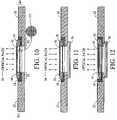
- FIG. 9is a top view of the wafer probe station shown in FIG. 1 illustrating a selective vacuum positioning system.
- FIG. 10is a cross sectional view of an optical chuck.
- FIG. 11is a cross sectional view of an alternative optical chuck.
- FIG. 12is a cross sectional view of yet another alternative optical chuck.
- the traditional approach to optical testinginvolves testing the inputs and outputs of a device-under-test with an optical sensor(s), a connector(s), and/or an electrical probe(s). Based upon using the sensor, the connector, and/or electrical probe the overall operational characteristics of the device-under-test may be characterized.
- the present inventorscame to the realization that together with optical testing there is a previously unrealized need to achieve performance levels that were previously not considered needed, namely ultra low noise and low current measurements.
- the present inventorsdetermined that unlike measuring the operational inputs and/or outputs of the device-under-test which are sufficiently accurately measured using only a shielded environment because the noise levels are relatively low and the current levels are relatively high, measurements of other electrical characteristics of the device-under-test apart from the operational inputs and/or outputs are desirable. For example, low current measurements with a high degree of accuracy may be desirable of a portion of the electrical aspects of the optical device-under-test, such as the leakage currents of a junction for a light emitting diode.
- FIG. 1illustrates a chuck 10 suitable for use with a support 12 within a probe station for testing a device-under-test.
- the perimeter region of the chuck 10is preferably electrically conductive and is supported around its periphery by an insulating member 18 .
- the insulating member 18maintains the chuck 10 in a fixed elevational position with respect to each other.
- the insulating member 18may include a handle 16 that passes through a slotted opening 20 to permit rotation of the chuck 10 , and hence the device-under-test supported thereon, for alignment.
- the insulating member 18 , and hence the chuck 10 supported thereonare slidably engaged with a conductive member 22 .
- the handle 16may extend from a slot 24 beneath the conductive member 22 .
- the handle 16may be used to laterally move the chuck 10 for easier loading and unloading of a device-under test on the chuck 10 .
- the conductive memberis at least partially laterally surrounding and/or at least laterally spaced apart from the chuck 10 and/or the insulating member 18 .
- probesmay be used to provide a test signal to the device under test or otherwise sense a signal from the device under test.
- An optical sensing device(not shown) may be included under the conductive member 22 within the region defined by the supports 29 . Alternatively, the optical sensing device may be included above the conductive member 22 or to the side thereof. As shown in FIG.
- the device-under-testmay be tested in an environment that includes a guard potential proximate thereof by connecting the conductive member 22 to the guard potential, which permits effective testing at leakage current levels not previously obtainable, nor thought desirable, with existing optical probes.
- the guarding of the optical chuck of FIG. 1resulted in a reduction greater than several orders of magnitude in stray capacitance (force to shield).
- the support 12may include one or more connectors 23 to the chuck 10 .
- the connector 23is preferably a co-axial or tri-axial connector providing a force test signal to the device under test. Also, multiple connectors 23 may be used to provide a Kelvin connection and/or a quasi-Kelvin connection to the device-under-test.
- the support 12may include one or more connectors 25 to provide a sense signal to the conductive member 22 .
- the guard braid on the connector 23 and/or connector 25may be electrically connected to the conductive member 22 .
- the chuck 10 designfacilitates improved testing of the device-under-test, at leakage current levels not previously considered obtainable, a tendency for breaking the device-under-test occurs when undergoing pressure as a result of probes.
- the device-under-testhas a tendency to warp or otherwise become non-uniform as a result of the central region of the device-under-test not being supported.
- the chuck 10may further include a central region having an optically transmissive (e.g., transparent) material 42 to the wavelength used for testing.
- the optically transmissive material 42is preferably co-planar (or substantially co-planar) with the chuck 10 supporting the device-under-test 40 so that the device-under-test is supported in face-to-face contact over at least a majority of its surface area. Also, the optically transmissive material 42 preferably occupies at least a majority of the lateral spatial extent of the opening (i.e., not the depth) defined by the chuck 10 . With the optically transmissive material 42 in the optical path of the device-under-test light may readily pass through the opening in the chuck 10 .
- the insulating member 18may include a raised portion 50 and an inset portion 52 .
- the raised portion 50forms a perimeter having an inner diameter substantially equal to the outer diameter of the chuck 10 which maintains the chuck 10 within the inset portion 52 .
- the inset portion 52preferably has an inner diameter substantially equal to the inner diameter of the chuck 10 so as to form a substantially continuous boundary for the optical path 34 .
- the conductive member 22may include a raised portion 60 and an inset portion 62 .
- the raised portion 60provides a surface having an inner shape, such as a pair of co-planar surfaces, substantially equal to the exterior width of the raised portion 50 of the insulating member 18 .
- the insulating member 18may be positioned within the conductive member 22 .
- the inset portion 62 of the conductive member 22has an inner diameter substantially equal to the inner diameter of the inset portion 52 and the chuck 10 so as to form a substantially continuous boundary for the optical path 34 .
- Devices within the optical path 34may include materials that are optically transparent to the wavelength of the optical signal.
- materials that are optically transparent to the wavelength of the optical signalare suitable for use as the optical chuck material 42 , such as for example, quartz, sapphire, lithium niobate, and silicon.
- the present inventorscame to the realization there exists a region which is substantially unguarded, namely, the region below the device under test. Initially it would seem that this region below the device-under-test will remain unguarded because placing a conductive member in the optical path would inhibit sensing the optical signal from the device or providing an optical signal to the device. After further consideration, the seemingly unavailability of a conductive member may be overcome by including an optically transmissive conductive material connected to a guard potential in the optical path below the device-under-test. Referring to FIG.
- a lower optically transmissive conductive material 70may be positioned in the optical path and electrically interconnected to the conductive member 22 to provide more complete guarding for the device-under-test, if desired.
- a non-conductive optically transparent material coated with an optically transparent material such as indium-tin-oxide, electrically interconnected to the conductive member 22may be used.
- the present inventorscame to the realization there exists a region which remains substantially unguarded, namely, the region above the device under test. Initially it would seem that this region above the device-under-test will remain unguarded because placing a conductive member in the optical path is seemingly difficult. After further consideration, the seemingly unavailability of a conductive member may be overcome by relocating the device-under-test and including an optically transmissive conductive material 74 in the optical path above the device-under-test, such as shown in FIG. 4 . Alternatively, a non-conductive optically transparent material coated with an optically transparent material, such as indium-tin-oxide, electrically interconnected to the conductive member 22 may be used.
- the orientation of the device-under-testis shown with the device-under-test on the top with the chuck thereunder. It is to be understood that the testing may be performed with the orientation of the device-under-test and/or chuck (etc.) in an inverted orientation.
- the preferred embodiment of the support 12provides a wafer supporting surface capable of providing a test signal and a guard member 22 that, in conjunction with the lower guard member 70 , allows the signal provided to or received from the device-under-test to be electrically guarded.
- the support 12also provides an environment suitable for low current low leakage measurements for an optical device so that the device-under test need not be transferred between an optical chuck in an optical probe station and a traditional chuck in an electrical probe station for the testing of optical components and electrical components, respectively, that may be included within the device-under-test.
- chucks used to support a DUT during both electrical and optical testingneeds to provide a stable surface where the DUT is held in place while testing is performed.
- a number of chucksappropriately called vacuum chucks, use vacuum pressure to hold the DUT in place.
- One problem with existing vacuum chucksis that when testing a DUT on a wafer that has been broken, the vacuum pressure provided by the chuck tends to deform the wafer because the chuck was only designed to hold a full wafer.
- an additional insulator 93may surround the conductive member 22 .
- the conductive member 22is preferably connected to a guard potential while the another conductive member 95 is connected to a shield potential.
- the shield potentialmay be provided in any suitable manner, such as for example, the shield braid of the connector 23 and/or the connector 25 .
- the another conductive member 95may extend to the optical path 34 .
- the another conductive member 95may be terminate prior to the optical path 34 .
- an optically transmissive conducive material or non-conductive optically transmissive material with a conductive coatingmay be provided within the optical path and connected to shield.
- yet another conductive member 95may be terminate prior to the optical path 34 .
- an optically transmissive conducive material or non-conductive optically transmissive material with a conductive coatinggenerally referred to as material 99 , may be provided within the optical path and connected to shield.
- the guard and/or shield environmentmay be extended in a lateral direction, and the guard and/or shield environment may be extended in a vertical direction, as desired.
- the chuck 10may include a vacuum chamber 100 comprising an approximate ring of about 270 degrees around the midpoint of the chuck 10 .
- the vacuum chamber 100may encircle the entire chuck or less than 270 degrees, as desired.
- a vacuum source(not shown) operates to provide a vacuum and is operatively connected to the vacuum chamber through vacuum supply lines 102 and 104 , a vacuum supply chamber 106 , and three vacuum shafts 108 . Vacuum pressure present within the vacuum chamber 108 is transmitted to the surface of the chuck 10 through small apertures 110 .
- the vacuum shafts 108are preferably positioned at 0 degrees, 90 degrees, and 270 degrees around the vacuum chamber 100 , respectively.
- a plug 112 each vacuum shaft, respectively,may be used to selectively isolate portions of the vacuum chamber 100 from the vacuum source. For example, if the vacuum source supplies vacuum pressure through vacuum supply line 104 , and the plugs 112 associated with the vacuum shafts 108 at 0 and 90 degrees respectively are activated, then a quarter section of the chuck is providing vacuum pressure to the wafer.
- the vacuum memberis supplying vacuum pressure through either vacuum supply line 102 or vacuum supply line 104 , or both, and the plugs 112 at 90 degrees and 270 degrees, respectively, are activated, then a half-section of the chuck is providing vacuum pressure to the wafer.
- the selective activation of different regions of the vacuum chamber of the chuck in non-concentric ringspermits fragments of a semiconductor device to be effectively tested. For example, if a fragment of a semiconductor is available then one or more regions may be interconnected to the vacuum source to maintain the fragment properly positioned on the chuck 10 . By disabling the vacuum for the non-used portions of the chuck the vacuum pressure may be more readily controlled and improves the vacuum by reducing leaks.
- the resulting vacuum pressure for the small apertures 110 under the device-under-testmay not sufficient vacuum pressure to maintain sufficient pressure.
- other patterns of vacuum holesmay likewise be used where groups of one or more vacuum holes may be selectively enabled.
- the different regionsmay include at least one of the same holes, if desired.
- the patterns of the vacuum holespreferably include at least one selectable region that is in a non-concentric region.
- a switching mechanismmay be used to select which of the vacuum regions provide a vacuum to the surface of the chuck.
- a selectable vacuum sourcemay be provided to each vacuum region.
- a pair of spaced apart transmissive plates with an opening defined therein to which a vacuum is providedmay be used with holes in the upper plate to provide a vacuum to the upper surface.
- using sufficiently thick spaced apart glass plates to provide structural integrity to the waferresults in excessive refraction of the optical signal.
- using sufficiently thin spaced apart glass platesresults in deflection of the supporting glass, and thus the wafer, which distorts the measurements.
- a pair of optically transmissive platespreferably include a web material, such as a honeycomb pattern, between the two plates to provide structural support.
- a web materialsuch as a honeycomb pattern
- the web materialextends between and interconnects the two plates to provide structural support.
- the web materialmay be in any suitable pattern, such as for example, a grid pattern or stripes.
- the web materialmay likewise provide selective vacuum zones to the upper surface.
Landscapes
- Physics & Mathematics (AREA)
- General Physics & Mathematics (AREA)
- Chemical & Material Sciences (AREA)
- Analytical Chemistry (AREA)
- Testing Or Measuring Of Semiconductors Or The Like (AREA)
Abstract
Description
Claims (4)
Priority Applications (2)
| Application Number | Priority Date | Filing Date | Title |
|---|---|---|---|
| US10/912,789US7268533B2 (en) | 2001-08-31 | 2004-08-06 | Optical testing device |
| US11/890,987US20070273387A1 (en) | 2001-08-31 | 2007-08-07 | Optical testing device |
Applications Claiming Priority (3)
| Application Number | Priority Date | Filing Date | Title |
|---|---|---|---|
| US31664401P | 2001-08-31 | 2001-08-31 | |
| US10/214,888US6836135B2 (en) | 2001-08-31 | 2002-08-07 | Optical testing device |
| US10/912,789US7268533B2 (en) | 2001-08-31 | 2004-08-06 | Optical testing device |
Related Parent Applications (1)
| Application Number | Title | Priority Date | Filing Date |
|---|---|---|---|
| US10/214,888ContinuationUS6836135B2 (en) | 2001-08-31 | 2002-08-07 | Optical testing device |
Related Child Applications (1)
| Application Number | Title | Priority Date | Filing Date |
|---|---|---|---|
| US11/890,987ContinuationUS20070273387A1 (en) | 2001-08-31 | 2007-08-07 | Optical testing device |
Publications (2)
| Publication Number | Publication Date |
|---|---|
| US20050007581A1 US20050007581A1 (en) | 2005-01-13 |
| US7268533B2true US7268533B2 (en) | 2007-09-11 |
Family
ID=23229978
Family Applications (3)
| Application Number | Title | Priority Date | Filing Date |
|---|---|---|---|
| US10/214,888Expired - Fee RelatedUS6836135B2 (en) | 2001-08-31 | 2002-08-07 | Optical testing device |
| US10/912,789Expired - Fee RelatedUS7268533B2 (en) | 2001-08-31 | 2004-08-06 | Optical testing device |
| US11/890,987AbandonedUS20070273387A1 (en) | 2001-08-31 | 2007-08-07 | Optical testing device |
Family Applications Before (1)
| Application Number | Title | Priority Date | Filing Date |
|---|---|---|---|
| US10/214,888Expired - Fee RelatedUS6836135B2 (en) | 2001-08-31 | 2002-08-07 | Optical testing device |
Family Applications After (1)
| Application Number | Title | Priority Date | Filing Date |
|---|---|---|---|
| US11/890,987AbandonedUS20070273387A1 (en) | 2001-08-31 | 2007-08-07 | Optical testing device |
Country Status (4)
| Country | Link |
|---|---|
| US (3) | US6836135B2 (en) |
| EP (1) | EP1432546A4 (en) |
| TW (1) | TWI265299B (en) |
| WO (1) | WO2003020467A1 (en) |
Cited By (4)
| Publication number | Priority date | Publication date | Assignee | Title |
|---|---|---|---|---|
| US20080224426A1 (en)* | 2007-03-16 | 2008-09-18 | Suss Microtec Test Systems Gmbh | Chuck with triaxial construction |
| US7969173B2 (en) | 2000-09-05 | 2011-06-28 | Cascade Microtech, Inc. | Chuck for holding a device under test |
| US8319503B2 (en) | 2008-11-24 | 2012-11-27 | Cascade Microtech, Inc. | Test apparatus for measuring a characteristic of a device under test |
| US9506973B2 (en) | 2010-06-07 | 2016-11-29 | Cascade Microtech, Inc. | High voltage chuck for a probe station |
Families Citing this family (32)
| Publication number | Priority date | Publication date | Assignee | Title |
|---|---|---|---|---|
| US6380751B2 (en) | 1992-06-11 | 2002-04-30 | Cascade Microtech, Inc. | Wafer probe station having environment control enclosure |
| US5345170A (en) | 1992-06-11 | 1994-09-06 | Cascade Microtech, Inc. | Wafer probe station having integrated guarding, Kelvin connection and shielding systems |
| US5561377A (en) | 1995-04-14 | 1996-10-01 | Cascade Microtech, Inc. | System for evaluating probing networks |
| US6002263A (en) | 1997-06-06 | 1999-12-14 | Cascade Microtech, Inc. | Probe station having inner and outer shielding |
| US6445202B1 (en) | 1999-06-30 | 2002-09-03 | Cascade Microtech, Inc. | Probe station thermal chuck with shielding for capacitive current |
| US6914423B2 (en) | 2000-09-05 | 2005-07-05 | Cascade Microtech, Inc. | Probe station |
| WO2003020467A1 (en) | 2001-08-31 | 2003-03-13 | Cascade Microtech, Inc. | Optical testing device |
| US6777964B2 (en) | 2002-01-25 | 2004-08-17 | Cascade Microtech, Inc. | Probe station |
| US6847219B1 (en) | 2002-11-08 | 2005-01-25 | Cascade Microtech, Inc. | Probe station with low noise characteristics |
| US7250779B2 (en) | 2002-11-25 | 2007-07-31 | Cascade Microtech, Inc. | Probe station with low inductance path |
| US6861856B2 (en)* | 2002-12-13 | 2005-03-01 | Cascade Microtech, Inc. | Guarded tub enclosure |
| US7221172B2 (en)* | 2003-05-06 | 2007-05-22 | Cascade Microtech, Inc. | Switched suspended conductor and connection |
| US7492172B2 (en) | 2003-05-23 | 2009-02-17 | Cascade Microtech, Inc. | Chuck for holding a device under test |
| DE10331565A1 (en)* | 2003-05-28 | 2004-12-30 | Osram Opto Semiconductors Gmbh | Wafer holding device for semiconductor chips in wafers has holed suction device on vacuum chamber that is transparent to electromagnetic radiation |
| US7250626B2 (en) | 2003-10-22 | 2007-07-31 | Cascade Microtech, Inc. | Probe testing structure |
| US7187188B2 (en) | 2003-12-24 | 2007-03-06 | Cascade Microtech, Inc. | Chuck with integrated wafer support |
| KR101141014B1 (en)* | 2004-03-08 | 2012-05-02 | 시옵티컬 인코포레이티드 | Wafer-level opto-electronic testing apparatus and method |
| WO2005121824A2 (en)* | 2004-06-07 | 2005-12-22 | Cascade Microtech, Inc. | Thermal optical chuck |
| US7330041B2 (en) | 2004-06-14 | 2008-02-12 | Cascade Microtech, Inc. | Localizing a temperature of a device for testing |
| SG162710A1 (en)* | 2004-12-27 | 2010-07-29 | Kulicke And Soffa Die Bonding | Apparatus for fixing a planar object, in particular a substrate, on a working area by means of vacuum |
| US7656172B2 (en) | 2005-01-31 | 2010-02-02 | Cascade Microtech, Inc. | System for testing semiconductors |
| US7535247B2 (en) | 2005-01-31 | 2009-05-19 | Cascade Microtech, Inc. | Interface for testing semiconductors |
| US9041851B2 (en)* | 2005-11-15 | 2015-05-26 | The Trustees Of Princeton University | Organic electronic detectors and methods of fabrication |
| DE102006038457B4 (en)* | 2006-08-16 | 2014-05-22 | Cascade Microtech, Inc. | Method and device for tempering electronic components |
| JP5495264B2 (en)* | 2010-03-17 | 2014-05-21 | パナソニックヘルスケア株式会社 | Container tray, tray base, and observation unit |
| US9201103B2 (en)* | 2011-08-09 | 2015-12-01 | Source Photonics, Inc. | Circuits, architectures, apparatuses, methods and algorithms for determining a DC bias in an AC or AC-coupled signal |
| WO2014042590A1 (en) | 2012-09-12 | 2014-03-20 | Heptagon Micro Optics Pte. Ltd. | Testing of optical devices |
| US9467604B2 (en) | 2012-12-03 | 2016-10-11 | Cognex Corporation | Method and apparatus for calibrating a camera lens flange to sensor distance |
| CN105751114B (en)* | 2016-04-05 | 2017-05-31 | 浙江鼎炬电子科技股份有限公司 | A kind of LED filament lamp carrier and its operating method |
| CN109807767B (en)* | 2017-11-20 | 2021-11-05 | 上海微电子装备(集团)股份有限公司 | Material holding device and material detection method |
| US10801969B1 (en)* | 2019-09-12 | 2020-10-13 | Lumentum Operations Llc | Testing device for bottom-emitting or bottom-detecting optical devices |
| US11231452B2 (en)* | 2020-02-04 | 2022-01-25 | Lumentum Operations Llc | Testing apparatus for optical devices |
Citations (512)
| Publication number | Priority date | Publication date | Assignee | Title |
|---|---|---|---|---|
| US1337866A (en) | 1917-09-27 | 1920-04-20 | Griffiths Ethel Grace | System for protecting electric cables |
| US2142625A (en) | 1932-07-06 | 1939-01-03 | Hollandsche Draad En Kabelfab | High tension cable |
| US2197081A (en) | 1937-06-14 | 1940-04-16 | Transit Res Corp | Motor support |
| US2376101A (en) | 1942-04-01 | 1945-05-15 | Ferris Instr Corp | Electrical energy transmission |
| US2389668A (en) | 1943-03-04 | 1945-11-27 | Barnes Drill Co | Indexing mechanism for machine tables |
| US2471897A (en) | 1945-01-13 | 1949-05-31 | Trico Products Corp | Fluid motor packing |
| US2812502A (en) | 1953-07-07 | 1957-11-05 | Bell Telephone Labor Inc | Transposed coaxial conductor system |
| US3176091A (en) | 1962-11-07 | 1965-03-30 | Helmer C Hanson | Controlled multiple switching unit |
| US3185927A (en) | 1961-01-31 | 1965-05-25 | Kulicke & Soffa Mfg Co | Probe instrument for inspecting semiconductor wafers including means for marking defective zones |
| US3193712A (en) | 1962-03-21 | 1965-07-06 | Clarence A Harris | High voltage cable |
| US3192844A (en)* | 1963-03-05 | 1965-07-06 | Kulicke And Soffa Mfg Company | Mask alignment fixture |
| US3201721A (en) | 1963-12-30 | 1965-08-17 | Western Electric Co | Coaxial line to strip line connector |
| US3230299A (en) | 1962-07-18 | 1966-01-18 | Gen Cable Corp | Electrical cable with chemically bonded rubber layers |
| US3256484A (en) | 1962-09-10 | 1966-06-14 | Tektronix Inc | High voltage test probe containing a part gas, part liquid dielectric fluid under pressure and having a transparent housing section for viewing the presence of the liquid therein |
| US3265969A (en) | 1960-04-19 | 1966-08-09 | Ipa Anstalt | High voltage probe apparatus with a plurality of discharge tube isolating spark gaps therein |
| US3289046A (en) | 1964-05-19 | 1966-11-29 | Gen Electric | Component chip mounted on substrate with heater pads therebetween |
| US3333274A (en) | 1965-04-21 | 1967-07-25 | Micro Tech Mfg Inc | Testing device |
| US3405361A (en) | 1964-01-08 | 1968-10-08 | Signetics Corp | Fluid actuable multi-point microprobe for semiconductors |
| US3408565A (en) | 1966-03-02 | 1968-10-29 | Philco Ford Corp | Apparatus for sequentially testing electrical components under controlled environmental conditions including a component support mating test head |
| US3435185A (en) | 1966-01-11 | 1969-03-25 | Rohr Corp | Sliding vacuum seal for electron beam welder |
| US3484679A (en) | 1966-10-03 | 1969-12-16 | North American Rockwell | Electrical apparatus for changing the effective capacitance of a cable |
| US3596228A (en) | 1969-05-29 | 1971-07-27 | Ibm | Fluid actuated contactor |
| US3602845A (en) | 1970-01-27 | 1971-08-31 | Us Army | Slot line nonreciprocal phase shifter |
| US3609539A (en) | 1968-09-28 | 1971-09-28 | Ibm | Self-aligning kelvin probe |
| US3648169A (en) | 1969-05-26 | 1972-03-07 | Teledyne Inc | Probe and head assembly |
| US3654573A (en) | 1970-06-29 | 1972-04-04 | Bell Telephone Labor Inc | Microwave transmission line termination |
| US3662318A (en) | 1970-12-23 | 1972-05-09 | Comp Generale Electricite | Transition device between coaxial and microstrip lines |
| US3710251A (en) | 1971-04-07 | 1973-01-09 | Collins Radio Co | Microelectric heat exchanger pedestal |
| US3714572A (en) | 1970-08-21 | 1973-01-30 | Rca Corp | Alignment and test fixture apparatus |
| US3775644A (en) | 1972-09-20 | 1973-11-27 | Communications Satellite Corp | Adjustable microstrip substrate holder |
| US3777260A (en) | 1972-12-14 | 1973-12-04 | Ibm | Grid for making electrical contact |
| US3810017A (en) | 1972-05-15 | 1974-05-07 | Teledyne Inc | Precision probe for testing micro-electronic units |
| US3814888A (en) | 1971-11-19 | 1974-06-04 | Gen Electric | Solid state induction cooking appliance |
| US3829076A (en) | 1972-06-08 | 1974-08-13 | H Sofy | Dial index machine |
| US3863181A (en) | 1973-12-03 | 1975-01-28 | Bell Telephone Labor Inc | Mode suppressor for strip transmission lines |
| US3866093A (en) | 1972-09-18 | 1975-02-11 | Norbert L Kusters | Low leakage electrical power input circuit for electromedical and other similar apparatus |
| US3930809A (en) | 1973-08-21 | 1976-01-06 | Wentworth Laboratories, Inc. | Assembly fixture for fixed point probe card |
| US3936743A (en) | 1974-03-05 | 1976-02-03 | Electroglas, Inc. | High speed precision chuck assembly |
| US3970934A (en) | 1974-08-12 | 1976-07-20 | Akin Aksu | Printed circuit board testing means |
| US3996517A (en) | 1975-12-29 | 1976-12-07 | Monsanto Company | Apparatus for wafer probing having surface level sensing |
| US4001685A (en) | 1974-03-04 | 1977-01-04 | Electroglas, Inc. | Micro-circuit test probe |
| US4008900A (en) | 1976-03-15 | 1977-02-22 | John Freedom | Indexing chuck |
| US4009456A (en) | 1970-10-07 | 1977-02-22 | General Microwave Corporation | Variable microwave attenuator |
| US4027253A (en) | 1973-05-18 | 1977-05-31 | Societe Lignes Telegraphiques Et Telephoniques | Non-reciprocal broadband slot line device |
| US4035723A (en) | 1975-10-16 | 1977-07-12 | Xynetics, Inc. | Probe arm |
| US4038894A (en) | 1975-07-18 | 1977-08-02 | Springfield Tool And Die, Inc. | Piercing apparatus |
| US4042119A (en) | 1975-06-30 | 1977-08-16 | International Business Machines Corporation | Workpiece positioning apparatus |
| US4049252A (en) | 1976-02-04 | 1977-09-20 | Bell Theodore F | Index table |
| US4093988A (en) | 1976-11-08 | 1978-06-06 | General Electric Company | High speed frequency response measurement |
| US4099120A (en) | 1976-04-19 | 1978-07-04 | Akin Aksu | Probe head for testing printed circuit boards |
| US4115735A (en) | 1976-10-14 | 1978-09-19 | Faultfinders, Inc. | Test fixture employing plural platens for advancing some or all of the probes of the test fixture |
| US4115736A (en) | 1977-03-09 | 1978-09-19 | The United States Of America As Represented By The Secretary Of The Air Force | Probe station |
| US4116523A (en) | 1976-01-23 | 1978-09-26 | James M. Foster | High frequency probe |
| JPS5352354Y2 (en) | 1974-05-23 | 1978-12-14 | ||
| US4151465A (en) | 1977-05-16 | 1979-04-24 | Lenz Seymour S | Variable flexure test probe for microelectronic circuits |
| US4161692A (en) | 1977-07-18 | 1979-07-17 | Cerprobe Corporation | Probe device for integrated circuit wafers |
| US4172993A (en) | 1978-09-13 | 1979-10-30 | The Singer Company | Environmental hood for testing printed circuit cards |
| WO1980000101A1 (en) | 1978-06-21 | 1980-01-24 | Cerprobe Corp | Probe and interface device for integrated circuit wafers |
| US4186338A (en) | 1976-12-16 | 1980-01-29 | Genrad, Inc. | Phase change detection method of and apparatus for current-tracing the location of faults on printed circuit boards and similar systems |
| DE2912826A1 (en) | 1979-03-30 | 1980-10-16 | Heinz Laass | Compact pair of electrical probes packaged for portability - are used for voltage or short circuit testing and clamped together, when not in use, by magnets |
| JPS567439Y2 (en) | 1975-09-20 | 1981-02-18 | ||
| US4275446A (en) | 1978-11-13 | 1981-06-23 | Siemens Aktiengesellschaft | Method and apparatus for measurement of attenuation and distortion by a test object |
| US4280112A (en) | 1979-02-21 | 1981-07-21 | Eisenhart Robert L | Electrical coupler |
| US4284033A (en) | 1979-10-31 | 1981-08-18 | Rca Corporation | Means to orbit and rotate target wafers supported on planet member |
| US4284682A (en) | 1980-04-30 | 1981-08-18 | Nasa | Heat sealable, flame and abrasion resistant coated fabric |
| US4287473A (en) | 1979-05-25 | 1981-09-01 | The United States Of America As Represented By The United States Department Of Energy | Nondestructive method for detecting defects in photodetector and solar cell devices |
| US4342958A (en) | 1980-03-28 | 1982-08-03 | Honeywell Information Systems Inc. | Automatic test equipment test probe contact isolation detection method |
| US4346355A (en) | 1980-11-17 | 1982-08-24 | Raytheon Company | Radio frequency energy launcher |
| US4352061A (en) | 1979-05-24 | 1982-09-28 | Fairchild Camera & Instrument Corp. | Universal test fixture employing interchangeable wired personalizers |
| US4357575A (en) | 1980-06-17 | 1982-11-02 | Dit-Mco International Corporation | Apparatus for use in testing printed circuit process boards having means for positioning such boards in proper juxtaposition with electrical contacting assemblies |
| DE3125552C1 (en) | 1981-06-29 | 1982-11-11 | Siemens AG, 1000 Berlin und 8000 München | Tester indicating voltage magnitude, polarity and testing continuity - has mains section and switchable reservoir enabling self-testing |
| US4365109A (en) | 1980-01-25 | 1982-12-21 | The United States Of America As Represented By The Secretary Of The Air Force | Coaxial cable design |
| US4365195A (en) | 1979-12-27 | 1982-12-21 | Communications Satellite Corporation | Coplanar waveguide mounting structure and test fixture for microwave integrated circuits |
| US4371742A (en) | 1977-12-20 | 1983-02-01 | Graham Magnetics, Inc. | EMI-Suppression from transmission lines |
| US4376920A (en) | 1981-04-01 | 1983-03-15 | Smith Kenneth L | Shielded radio frequency transmission cable |
| US4383178A (en) | 1980-04-11 | 1983-05-10 | Hitachi, Ltd. | System for driving rotary member in vacuum |
| US4414638A (en) | 1981-04-30 | 1983-11-08 | Dranetz Engineering Laboratories, Inc. | Sampling network analyzer with stored correction of gain errors |
| US4419626A (en) | 1981-08-25 | 1983-12-06 | Daymarc Corporation | Broad band contactor assembly for testing integrated circuit devices |
| US4425395A (en) | 1981-04-30 | 1984-01-10 | Fujikura Rubber Works, Ltd. | Base fabrics for polyurethane-coated fabrics, polyurethane-coated fabrics and processes for their production |
| US4426619A (en) | 1981-06-03 | 1984-01-17 | Temptronic Corporation | Electrical testing system including plastic window test chamber and method of using same |
| US4479690A (en) | 1982-09-13 | 1984-10-30 | The United States Of America As Represented By The Secretary Of The Navy | Underwater splice for submarine coaxial cable |
| US4480223A (en) | 1981-11-25 | 1984-10-30 | Seiichiro Aigo | Unitary probe assembly |
| US4487996A (en) | 1982-12-02 | 1984-12-11 | Electric Power Research Institute, Inc. | Shielded electrical cable |
| US4491173A (en) | 1982-05-28 | 1985-01-01 | Temptronic Corporation | Rotatable inspection table |
| US4503335A (en) | 1981-04-13 | 1985-03-05 | Canon Kabushiki Kaisha | Semiconductor printing apparatus with multiple independent temperature control |
| US4507602A (en) | 1982-08-13 | 1985-03-26 | The United States Of America As Represented By The Secretary Of The Air Force | Measurement of permittivity and permeability of microwave materials |
| JPS6071425U (en) | 1983-10-25 | 1985-05-20 | 株式会社アマダ | Mounting structure of upper apron in press machine |
| EP0087497A3 (en) | 1982-02-15 | 1985-07-03 | Spencer Products Company | Tape measure |
| US4528504A (en) | 1982-05-27 | 1985-07-09 | Harris Corporation | Pulsed linear integrated circuit tester |
| US4531474A (en) | 1983-06-04 | 1985-07-30 | Dainippon Screen Manufacturing Co., Ltd. | Rotary board treating apparatus |
| US4532423A (en) | 1982-05-31 | 1985-07-30 | Tokyo Shibaura Denki Kabushiki Kaisha | IC Tester using an electron beam capable of easily setting a probe card unit for wafers & packaged IC's to be tested |
| US4557599A (en) | 1984-03-06 | 1985-12-10 | General Signal Corporation | Calibration and alignment target plate |
| US4566184A (en) | 1981-08-24 | 1986-01-28 | Rockwell International Corporation | Process for making a probe for high speed integrated circuits |
| US4567321A (en) | 1984-02-20 | 1986-01-28 | Junkosha Co., Ltd. | Flexible flat cable |
| US4567908A (en) | 1983-05-31 | 1986-02-04 | Contraves Ag | Discharge system and method of operating same |
| US4575676A (en) | 1983-04-04 | 1986-03-11 | Advanced Research And Applications Corporation | Method and apparatus for radiation testing of electron devices |
| US4588970A (en) | 1984-01-09 | 1986-05-13 | Hewlett-Packard Company | Three section termination for an R.F. triaxial directional bridge |
| US4621169A (en) | 1983-06-21 | 1986-11-04 | Compagnie Francaise De Raffinage | Electric cable construction and uses therefor |
| US4626618A (en) | 1984-05-08 | 1986-12-02 | Fujikura Ltd. | DC electric power cable |
| WO1986007493A1 (en) | 1985-06-13 | 1986-12-18 | Plessey Overseas Limited | Calibration apparatus for integrated circuits |
| US4642417A (en) | 1984-07-30 | 1987-02-10 | Kraftwerk Union Aktiengesellschaft | Concentric three-conductor cable |
| US4646005A (en) | 1984-03-16 | 1987-02-24 | Motorola, Inc. | Signal probe |
| JPS6211243B2 (en) | 1982-12-14 | 1987-03-11 | Matsushita Electric Ind Co Ltd | |
| US4665360A (en) | 1985-03-11 | 1987-05-12 | Eaton Corporation | Docking apparatus |
| US4673839A (en) | 1986-09-08 | 1987-06-16 | Tektronix, Inc. | Piezoelectric pressure sensing apparatus for integrated circuit testing stations |
| US4675600A (en) | 1984-05-17 | 1987-06-23 | Geo International Corporation | Testing apparatus for plated through-holes on printed circuit boards, and probe therefor |
| US4680538A (en) | 1985-01-15 | 1987-07-14 | Cornell Research Foundation, Inc. | Millimeter wave vector network analyzer |
| US4684883A (en) | 1985-05-13 | 1987-08-04 | American Telephone And Telegraph Company, At&T Bell Laboratories | Method of manufacturing high-quality semiconductor light-emitting devices |
| US4691831A (en) | 1984-06-25 | 1987-09-08 | Takeda Riken Co., Ltd. | IC test equipment |
| US4694245A (en) | 1984-09-07 | 1987-09-15 | Precision Drilling, Inc. | Vacuum-actuated top access test probe fixture |
| US4695794A (en) | 1985-05-31 | 1987-09-22 | Santa Barbara Research Center | Voltage calibration in E-beam probe using optical flooding |
| US4697143A (en) | 1984-04-30 | 1987-09-29 | Cascade Microtech, Inc. | Wafer probe |
| US4703433A (en) | 1984-01-09 | 1987-10-27 | Hewlett-Packard Company | Vector network analyzer with integral processor |
| US4711563A (en) | 1987-02-11 | 1987-12-08 | Lass Bennett D | Portable collapsible darkroom |
| US4712370A (en) | 1986-04-24 | 1987-12-15 | The United States Of America As Represented By The Secretary Of The Air Force | Sliding duct seal |
| US4727637A (en) | 1987-01-20 | 1988-03-01 | The Boeing Company | Computer aided connector assembly method and apparatus |
| US4730158A (en) | 1986-06-06 | 1988-03-08 | Santa Barbara Research Center | Electron-beam probing of photodiodes |
| US4731577A (en) | 1987-03-05 | 1988-03-15 | Logan John K | Coaxial probe card |
| US4734872A (en) | 1985-04-30 | 1988-03-29 | Temptronic Corporation | Temperature control for device under test |
| US4739259A (en) | 1986-08-01 | 1988-04-19 | Tektronix, Inc. | Telescoping pin probe |
| US4744041A (en) | 1985-03-04 | 1988-05-10 | International Business Machines Corporation | Method for testing DC motors |
| GB2197081A (en) | 1986-11-07 | 1988-05-11 | Plessey Co Plc | Coplanar waveguide probe |
| US4755874A (en) | 1987-08-31 | 1988-07-05 | Kla Instruments Corporation | Emission microscopy system |
| US4755746A (en) | 1985-04-24 | 1988-07-05 | Prometrix Corporation | Apparatus and methods for semiconductor wafer testing |
| US4757255A (en) | 1986-03-03 | 1988-07-12 | National Semiconductor Corporation | Environmental box for automated wafer probing |
| US4758785A (en) | 1986-09-03 | 1988-07-19 | Tektronix, Inc. | Pressure control apparatus for use in an integrated circuit testing station |
| US4759712A (en) | 1986-10-17 | 1988-07-26 | Temptronic Corporation | Device for applying controlled temperature stimuli to nerve sensitive tissue |
| US4771234A (en) | 1986-11-20 | 1988-09-13 | Hewlett-Packard Company | Vacuum actuated test fixture |
| US4772846A (en) | 1986-12-29 | 1988-09-20 | Hughes Aircraft Company | Wafer alignment and positioning apparatus for chip testing by voltage contrast electron microscopy |
| JPS63143814U (en) | 1987-03-12 | 1988-09-21 | ||
| US4777434A (en) | 1985-10-03 | 1988-10-11 | Amp Incorporated | Microelectronic burn-in system |
| JPS63160355U (en) | 1987-04-08 | 1988-10-20 | ||
| US4783625A (en) | 1986-08-21 | 1988-11-08 | Tektronix, Inc. | Wideband high impedance card mountable probe |
| US4784213A (en) | 1986-04-08 | 1988-11-15 | Temptronic Corporation | Mixing valve air source |
| US4786867A (en) | 1986-09-02 | 1988-11-22 | Canon Kabushiki Kaisha | Wafer prober |
| US4787752A (en) | 1986-10-24 | 1988-11-29 | Fts Systems, Inc. | Live component temperature conditioning device providing fast temperature variations |
| US4791363A (en) | 1987-09-28 | 1988-12-13 | Logan John K | Ceramic microstrip probe blade |
| US4810981A (en) | 1987-06-04 | 1989-03-07 | General Microwave Corporation | Assembly of microwave components |
| US4812754A (en) | 1987-01-07 | 1989-03-14 | Tracy Theodore A | Circuit board interfacing apparatus |
| US4816767A (en) | 1984-01-09 | 1989-03-28 | Hewlett-Packard Company | Vector network analyzer with integral processor |
| US4818169A (en) | 1985-05-17 | 1989-04-04 | Schram Richard R | Automated wafer inspection system |
| US4827211A (en) | 1987-01-30 | 1989-05-02 | Cascade Microtech, Inc. | Wafer probe |
| EP0314481A1 (en) | 1987-10-28 | 1989-05-03 | Irish Transformers Limited | A temperature control instrument for electronic components under test |
| WO1989004001A1 (en) | 1987-10-27 | 1989-05-05 | Martin Marietta Corporation | Calibrating method for apparatus evaluating microwave/millimeter wave circuits |
| US4838802A (en) | 1987-07-08 | 1989-06-13 | Tektronix, Inc. | Low inductance ground lead |
| US4839587A (en) | 1988-03-29 | 1989-06-13 | Digital Equipment Corporation | Test fixture for tab circuits and devices |
| JPH01165968A (en) | 1987-12-22 | 1989-06-29 | Mitsubishi Electric Corp | Wafer probing apparatus |
| US4845426A (en) | 1987-05-20 | 1989-07-04 | Signatone Corporation | Temperature conditioner for tests of unpackaged semiconductors |
| US4849689A (en) | 1988-11-04 | 1989-07-18 | Cascade Microtech, Inc. | Microwave wafer probe having replaceable probe tip |
| US4856904A (en) | 1985-01-21 | 1989-08-15 | Nikon Corporation | Wafer inspecting apparatus |
| US4858160A (en) | 1988-03-18 | 1989-08-15 | Cascade Microtech, Inc. | System for setting reference reactance for vector corrected measurements |
| US4856426A (en) | 1984-05-26 | 1989-08-15 | Heidelberger Druckmaschinen Ag | Sheet-fed rotary printing machine with printing units arranged in tandem |
| US4859989A (en) | 1987-12-01 | 1989-08-22 | W. L. Gore & Associates, Inc. | Security system and signal carrying member thereof |
| JPH01209380A (en) | 1988-02-16 | 1989-08-23 | Fujitsu Ltd | Probe card |
| JPH01214038A (en) | 1988-02-22 | 1989-08-28 | Mitsubishi Electric Corp | probe card |
| JPH01219575A (en) | 1988-02-27 | 1989-09-01 | Anritsu Corp | High frequency characteristic measuring instrument |
| US4871883A (en) | 1986-07-29 | 1989-10-03 | W. L. Gore & Associates, Inc. | Electro-magnetic shielding |
| US4871965A (en) | 1987-03-16 | 1989-10-03 | Apex Microtechnology Corporation | Environmental testing facility for electronic components |
| US4884206A (en) | 1984-12-21 | 1989-11-28 | Bendix Electronics S.A. | Process and processing circuit for the analog output signal of a sensor |
| US4884026A (en) | 1987-06-24 | 1989-11-28 | Tokyo Electron Limited | Electrical characteristic measuring apparatus |
| JPH01296167A (en) | 1988-05-24 | 1989-11-29 | Mitsubishi Electric Corp | Probe card |
| US4888550A (en) | 1981-09-14 | 1989-12-19 | Texas Instruments Incorporated | Intelligent multiprobe tip |
| JPH01178872U (en) | 1988-06-04 | 1989-12-21 | ||
| US4894612A (en) | 1987-08-13 | 1990-01-16 | Hypres, Incorporated | Soft probe for providing high speed on-wafer connections to a circuit |
| US4893914A (en) | 1988-10-12 | 1990-01-16 | The Micromanipulator Company, Inc. | Test station |
| US4896109A (en) | 1987-12-07 | 1990-01-23 | The United States Of America As Represented By The Department Of Energy | Photoconductive circuit element reflectometer |
| US4899998A (en) | 1987-11-10 | 1990-02-13 | Hiroshi Teramachi | Rotational positioning device |
| US4904933A (en) | 1986-09-08 | 1990-02-27 | Tektronix, Inc. | Integrated circuit probe station |
| US4904935A (en) | 1988-11-14 | 1990-02-27 | Eaton Corporation | Electrical circuit board text fixture having movable platens |
| US4906920A (en) | 1988-10-11 | 1990-03-06 | Hewlett-Packard Company | Self-leveling membrane probe |
| US4916398A (en) | 1988-12-21 | 1990-04-10 | Spectroscopy Imaging Systems Corp. | Efficient remote transmission line probe tuning for NMR apparatus |
| US4918279A (en) | 1987-08-28 | 1990-04-17 | Charmilles Technologies, S.A. | EDM cutting machine including device for preventing transmission of sealing plate movement to guide head arm |
| US4918374A (en) | 1988-10-05 | 1990-04-17 | Applied Precision, Inc. | Method and apparatus for inspecting integrated circuit probe cards |
| US4923407A (en) | 1989-10-02 | 1990-05-08 | Tektronix, Inc. | Adjustable low inductance probe |
| US4926118A (en) | 1988-02-22 | 1990-05-15 | Sym-Tek Systems, Inc. | Test station |
| US4933634A (en) | 1988-01-22 | 1990-06-12 | Commissariat A L'energie Atomique | Device and method to measure a short radiation pulse or an electric pulse |
| JPH0222837Y2 (en) | 1983-12-26 | 1990-06-20 | ||
| JPH0222873Y2 (en) | 1981-02-09 | 1990-06-20 | ||
| JPH02220453A (en) | 1989-02-21 | 1990-09-03 | Nippon Telegr & Teleph Corp <Ntt> | Apparatus for inspecting electronic circuit on wafer |
| US4968931A (en) | 1989-11-03 | 1990-11-06 | Motorola, Inc. | Apparatus and method for burning in integrated circuit wafers |
| US4978907A (en) | 1989-05-10 | 1990-12-18 | At&T Bell Laboratories | Apparatus and method for expanding the frequency range over which electrical signal amplitudes can be accurately measured |
| US4978914A (en) | 1988-03-15 | 1990-12-18 | Furukawa Denki Kogyo Kabushiki Kaisha | Laminated board for testing electronic components |
| US4982153A (en) | 1989-02-06 | 1991-01-01 | Cray Research, Inc. | Method and apparatus for cooling an integrated circuit chip during testing |
| US4994737A (en) | 1990-03-09 | 1991-02-19 | Cascade Microtech, Inc. | System for facilitating planar probe measurements of high-speed interconnect structures |
| US5001423A (en) | 1990-01-24 | 1991-03-19 | International Business Machines Corporation | Dry interface thermal chuck temperature control system for semiconductor wafer testing |
| US5010296A (en) | 1989-12-13 | 1991-04-23 | Mitsubishi Denki Kabushiki Kaisha | Wafer prober |
| US5019692A (en) | 1990-03-29 | 1991-05-28 | Eastman Kodak Company | Thermostatic device for fuser |
| US5030907A (en) | 1989-05-19 | 1991-07-09 | Knights Technology, Inc. | CAD driven microprobe integrated circuit tester |
| US5034688A (en) | 1988-05-05 | 1991-07-23 | Ets Gourdon | Temperature conditioning support for small objects such as semi-conductor components and thermal regulation process using said support |
| JPH03175367A (en) | 1989-12-04 | 1991-07-30 | Sharp Corp | Measuring jig for dc characteristic of semiconductor device |
| US5041782A (en) | 1989-09-20 | 1991-08-20 | Design Technique International, Inc. | Microstrip probe |
| US5045781A (en) | 1989-06-08 | 1991-09-03 | Cascade Microtech, Inc. | High-frequency active probe having replaceable contact needles |
| JPH0367187B2 (en) | 1984-04-17 | 1991-10-22 | Nissan Motor | |
| US5061823A (en) | 1990-07-13 | 1991-10-29 | W. L. Gore & Associates, Inc. | Crush-resistant coaxial transmission line |
| US5065092A (en) | 1990-05-14 | 1991-11-12 | Triple S Engineering, Inc. | System for locating probe tips on an integrated circuit probe card and method therefor |
| US5065089A (en) | 1990-06-01 | 1991-11-12 | Tovex Tech, Inc. | Circuit handler with sectioned rail |
| US5066357A (en) | 1990-01-11 | 1991-11-19 | Hewlett-Packard Company | Method for making flexible circuit card with laser-contoured vias and machined capacitors |
| US5070297A (en) | 1990-06-04 | 1991-12-03 | Texas Instruments Incorporated | Full wafer integrated circuit testing device |
| US5077523A (en) | 1989-11-03 | 1991-12-31 | John H. Blanz Company, Inc. | Cryogenic probe station having movable chuck accomodating variable thickness probe cards |
| JPH04732Y2 (en) | 1986-03-31 | 1992-01-10 | ||
| US5084671A (en) | 1987-09-02 | 1992-01-28 | Tokyo Electron Limited | Electric probing-test machine having a cooling system |
| US5089774A (en) | 1989-12-26 | 1992-02-18 | Sharp Kabushiki Kaisha | Apparatus and a method for checking a semiconductor |
| US5091691A (en) | 1988-03-21 | 1992-02-25 | Semitest, Inc. | Apparatus for making surface photovoltage measurements of a semiconductor |
| US5095891A (en) | 1986-07-10 | 1992-03-17 | Siemens Aktiengesellschaft | Connecting cable for use with a pulse generator and a shock wave generator |
| US5097207A (en) | 1989-11-03 | 1992-03-17 | John H. Blanz Company, Inc. | Temperature stable cryogenic probe station |
| US5101149A (en) | 1989-07-18 | 1992-03-31 | National Semiconductor Corporation | Modifiable IC board |
| US5101453A (en) | 1991-07-05 | 1992-03-31 | Cascade Microtech, Inc. | Fiber optic wafer probe |
| US5103169A (en) | 1989-11-15 | 1992-04-07 | Texas Instruments Incorporated | Relayless interconnections in high performance signal paths |
| US5105181A (en) | 1990-08-17 | 1992-04-14 | Hydro-Quebec | Method and electrical measuring apparatus for analyzing the impedance of the source of an actual alternating voltage |
| US5105148A (en) | 1991-01-24 | 1992-04-14 | Itt Corporation | Replaceable tip test probe |
| US5107076A (en) | 1991-01-08 | 1992-04-21 | W. L. Gore & Associates, Inc. | Easy strip composite dielectric coaxial signal cable |
| EP0460911A3 (en) | 1990-06-08 | 1992-08-19 | Cascade Microtech, Inc. | Electrical probe with contact force protection |
| US5142224A (en) | 1988-12-13 | 1992-08-25 | Comsat | Non-destructive semiconductor wafer probing system using laser pulses to generate and detect millimeter wave signals |
| US5144228A (en) | 1991-04-23 | 1992-09-01 | International Business Machines Corporation | Probe interface assembly |
| US5160883A (en) | 1989-11-03 | 1992-11-03 | John H. Blanz Company, Inc. | Test station having vibrationally stabilized X, Y and Z movable integrated circuit receiving support |
| US5159752A (en) | 1989-03-22 | 1992-11-03 | Texas Instruments Incorporated | Scanning electron microscope based parametric testing method and apparatus |
| US5164661A (en) | 1991-05-31 | 1992-11-17 | Ej Systems, Inc. | Thermal control system for a semi-conductor burn-in |
| US5166606A (en) | 1989-11-03 | 1992-11-24 | John H. Blanz Company, Inc. | High efficiency cryogenic test station |
| US5172049A (en) | 1990-10-15 | 1992-12-15 | Advantest Corporation | IC test equipment |
| US5198752A (en) | 1987-09-02 | 1993-03-30 | Tokyo Electron Limited | Electric probing-test machine having a cooling system |
| US5198753A (en) | 1990-06-29 | 1993-03-30 | Digital Equipment Corporation | Integrated circuit test fixture and method |
| US5198756A (en) | 1991-07-29 | 1993-03-30 | Atg-Electronics Inc. | Test fixture wiring integrity verification device |
| US5198758A (en) | 1991-09-23 | 1993-03-30 | Digital Equipment Corp. | Method and apparatus for complete functional testing of a complex signal path of a semiconductor chip |
| US5202558A (en) | 1992-03-04 | 1993-04-13 | Barker Lynn M | Flexible fiber optic probe for high-pressure shock experiments |
| US5210485A (en) | 1991-07-26 | 1993-05-11 | International Business Machines Corporation | Probe for wafer burn-in test system |
| US5214243A (en) | 1991-10-11 | 1993-05-25 | Endevco Corporation | High-temperature, low-noise coaxial cable assembly with high strength reinforcement braid |
| US5214374A (en) | 1991-12-12 | 1993-05-25 | Everett/Charles Contact Products, Inc. | Dual level test fixture |
| US5218185A (en) | 1989-08-15 | 1993-06-08 | Trustees Of The Thomas A. D. Gross 1988 Revocable Trust | Elimination of potentially harmful electrical and magnetic fields from electric blankets and other electrical appliances |
| US5220277A (en) | 1991-03-26 | 1993-06-15 | Erich Reitinger | Arrangement for testing semiconductor wafers or the like |
| US5221905A (en) | 1992-02-28 | 1993-06-22 | International Business Machines Corporation | Test system with reduced test contact interface resistance |
| JPH05157790A (en) | 1991-12-04 | 1993-06-25 | Tokyo Kasoode Kenkyusho:Kk | Device for inspecting probe card |
| JPH05166893A (en) | 1991-12-17 | 1993-07-02 | Tokyo Kasoode Kenkyusho:Kk | Probe card inspecting device |
| US5225796A (en) | 1992-01-27 | 1993-07-06 | Tektronix, Inc. | Coplanar transmission structure having spurious mode suppression |
| US5225037A (en) | 1991-06-04 | 1993-07-06 | Texas Instruments Incorporated | Method for fabrication of probe card for testing of semiconductor devices |
| US5237267A (en) | 1992-05-29 | 1993-08-17 | Cascade Microtech, Inc. | Wafer probe station having auxiliary chucks |
| US5266889A (en)* | 1992-05-29 | 1993-11-30 | Cascade Microtech, Inc. | Wafer probe station with integrated environment control enclosure |
| US5278494A (en) | 1991-02-19 | 1994-01-11 | Tokyo Electron Yamanashi Limited | Wafer probing test machine |
| US5280156A (en) | 1990-12-25 | 1994-01-18 | Ngk Insulators, Ltd. | Wafer heating apparatus and with ceramic substrate and dielectric layer having electrostatic chucking means |
| US5303938A (en) | 1993-03-25 | 1994-04-19 | Miller Donald C | Kelvin chuck apparatus and method of manufacture |
| US5309088A (en) | 1990-08-10 | 1994-05-03 | Texas Instruments Incorporated | Measurement of semiconductor parameters at cryogenic temperatures using a spring contact probe |
| US5315237A (en) | 1990-08-06 | 1994-05-24 | Tokyo Electron Limited | Touch sensor unit of prober for testing electric circuit and electric circuit testing apparatus using the touch sensor unit |
| US5321352A (en) | 1991-08-01 | 1994-06-14 | Tokyo Electron Yamanashi Limited | Probe apparatus and method of alignment for the same |
| US5325052A (en) | 1990-11-30 | 1994-06-28 | Tokyo Electron Yamanashi Limited | Probe apparatus |
| US5334931A (en) | 1991-11-12 | 1994-08-02 | International Business Machines Corporation | Molded test probe assembly |
| US5336989A (en) | 1991-09-19 | 1994-08-09 | Audio Presicion | AC mains test apparatus and method |
| US5345170A (en) | 1992-06-11 | 1994-09-06 | Cascade Microtech, Inc. | Wafer probe station having integrated guarding, Kelvin connection and shielding systems |
| DE4316111A1 (en) | 1993-05-13 | 1994-11-17 | Ehlermann Eckhard | Integrated circuit test board suitable for high-temperature measurements |
| US5369370A (en) | 1990-06-13 | 1994-11-29 | Max-Planck-Institut Fuer Eisenforschung Gmbh | Method and apparatus for the measurement of the corrosion potential between a coated metal surface and a reference electrode |
| US5371457A (en) | 1991-02-12 | 1994-12-06 | Lipp; Robert J. | Method and apparatus to test for current in an integrated circuit |
| US5373231A (en) | 1993-06-10 | 1994-12-13 | G. G. B. Industries, Inc. | Integrated circuit probing apparatus including a capacitor bypass structure |
| US5382898A (en) | 1992-09-21 | 1995-01-17 | Cerprobe Corporation | High density probe card for testing electrical circuits |
| JPH075197Y2 (en) | 1988-04-27 | 1995-02-08 | 立川ブラインド工業株式会社 | Slat rotation device for folding shutter |
| US5397855A (en) | 1992-09-08 | 1995-03-14 | Filotex | Low noise cable |
| US5404111A (en)* | 1991-08-03 | 1995-04-04 | Tokyo Electron Limited | Probe apparatus with a swinging holder for an object of examination |
| US5408189A (en) | 1990-05-25 | 1995-04-18 | Everett Charles Technologies, Inc. | Test fixture alignment system for printed circuit boards |
| US5410259A (en) | 1992-06-01 | 1995-04-25 | Tokyo Electron Yamanashi Limited | Probing device setting a probe card parallel |
| US5422574A (en) | 1993-01-14 | 1995-06-06 | Probe Technology Corporation | Large scale protrusion membrane for semiconductor devices under test with very high pin counts |
| DE9406227U1 (en) | 1994-04-14 | 1995-08-31 | Meyer Fa Rud Otto | Temperature change test device |
| US5451884A (en) | 1993-08-04 | 1995-09-19 | Transat Corp. | Electronic component temperature test system with flat ring revolving carriage |
| JPH07273509A (en) | 1994-04-04 | 1995-10-20 | Toshiba Corp | Method for manufacturing microwave circuit and circuit board |
| US5461328A (en) | 1992-02-07 | 1995-10-24 | Micron Technology, Inc. | Fixture for burn-in testing of semiconductor wafers |
| US5469324A (en) | 1994-10-07 | 1995-11-21 | Storage Technology Corporation | Integrated decoupling capacitive core for a printed circuit board and method of making same |
| US5475316A (en) | 1993-12-27 | 1995-12-12 | Hypervision, Inc. | Transportable image emission microscope |
| US5477011A (en) | 1994-03-03 | 1995-12-19 | W. L. Gore & Associates, Inc. | Low noise signal transmission cable |
| US5479108A (en) | 1992-11-25 | 1995-12-26 | David Cheng | Method and apparatus for handling wafers |
| US5479109A (en) | 1992-06-03 | 1995-12-26 | Trw Inc. | Testing device for integrated circuits on wafer |
| US5481936A (en) | 1993-06-29 | 1996-01-09 | Yugen Kaisha Sozoan | Rotary drive positioning system for an indexing table |
| US5486975A (en) | 1994-01-31 | 1996-01-23 | Applied Materials, Inc. | Corrosion resistant electrostatic chuck |
| US5488954A (en) | 1994-09-09 | 1996-02-06 | Georgia Tech Research Corp. | Ultrasonic transducer and method for using same |
| US5491426A (en) | 1994-06-30 | 1996-02-13 | Vlsi Technology, Inc. | Adaptable wafer probe assembly for testing ICs with different power/ground bond pad configurations |
| US5493070A (en) | 1993-07-28 | 1996-02-20 | Hewlett-Packard Company | Measuring cable and measuring system |
| US5493236A (en) | 1993-06-23 | 1996-02-20 | Mitsubishi Denki Kabushiki Kaisha | Test analysis apparatus and analysis method for semiconductor wafer using OBIC analysis |
| US5500606A (en) | 1993-09-16 | 1996-03-19 | Compaq Computer Corporation | Completely wireless dual-access test fixture |
| US5506515A (en) | 1994-07-20 | 1996-04-09 | Cascade Microtech, Inc. | High-frequency probe tip assembly |
| EP0706210A1 (en) | 1994-09-13 | 1996-04-10 | Hughes Aircraft Company | Transparent optical chuck incorporating optical monitoring |
| US5508631A (en) | 1994-10-27 | 1996-04-16 | Mitel Corporation | Semiconductor test chip with on wafer switching matrix |
| US5510792A (en) | 1993-12-27 | 1996-04-23 | Tdk Corporation | Anechoic chamber and wave absorber |
| US5511010A (en) | 1994-06-10 | 1996-04-23 | Texas Instruments Incorporated | Method and apparatus of eliminating interference in an undersettled electrical signal |
| US5517111A (en) | 1995-03-16 | 1996-05-14 | Phase Metrics | Automatic testing system for magnetoresistive heads |
| US5521522A (en) | 1992-11-13 | 1996-05-28 | Tokyo Electron Limited | Probe apparatus for testing multiple integrated circuit dies |
| US5523694A (en) | 1994-04-08 | 1996-06-04 | Cole, Jr.; Edward I. | Integrated circuit failure analysis by low-energy charge-induced voltage alteration |
| US5530372A (en) | 1994-04-15 | 1996-06-25 | Schlumberger Technologies, Inc. | Method of probing a net of an IC at an optimal probe-point |
| US5530371A (en) | 1994-04-15 | 1996-06-25 | International Business Machines Corporation | Probe card assembly |
| US5539323A (en) | 1993-05-07 | 1996-07-23 | Brooks Automation, Inc. | Sensor for articles such as wafers on end effector |
| US5550482A (en) | 1993-07-20 | 1996-08-27 | Tokyo Electron Kabushiki Kaisha | Probe device |
| US5550480A (en) | 1994-07-05 | 1996-08-27 | Motorola, Inc. | Method and means for controlling movement of a chuck in a test apparatus |
| US5552716A (en) | 1993-03-15 | 1996-09-03 | Hamamatsu Photonics K.K. | Method of positioning an electrooptic probe of an apparatus for the measurement of voltage |
| US5561377A (en) | 1995-04-14 | 1996-10-01 | Cascade Microtech, Inc. | System for evaluating probing networks |
| US5561585A (en) | 1993-12-20 | 1996-10-01 | International Business Machines Corporation | Electrostatic chuck with reference electrode |
| US5565788A (en) | 1994-07-20 | 1996-10-15 | Cascade Microtech, Inc. | Coaxial wafer probe with tip shielding |
| US5572398A (en) | 1994-11-14 | 1996-11-05 | Hewlett-Packard Co. | Tri-polar electrostatic chuck |
| US5571324A (en) | 1993-07-26 | 1996-11-05 | Tokyo Ohka Kogyo Co., Ltd. | Rotary-cup coating apparatus |
| US5583445A (en) | 1994-02-04 | 1996-12-10 | Hughes Aircraft Company | Opto-electronic membrane probe |
| US5594358A (en) | 1993-09-02 | 1997-01-14 | Matsushita Electric Industrial Co., Ltd. | Radio frequency probe and probe card including a signal needle and grounding needle coupled to a microstrip transmission line |
| US5610529A (en) | 1995-04-28 | 1997-03-11 | Cascade Microtech, Inc. | Probe station having conductive coating added to thermal chuck insulator |
| US5611946A (en) | 1994-02-18 | 1997-03-18 | New Wave Research | Multi-wavelength laser system, probe station and laser cutter system using the same |
| US5617035A (en) | 1993-11-01 | 1997-04-01 | Motorola, Inc. | Method for testing integrated devices |
| US5631571A (en) | 1996-04-03 | 1997-05-20 | The United States Of America As Represented By The Secretary Of The Air Force | Infrared receiver wafer level probe testing |
| US5640101A (en) | 1994-03-31 | 1997-06-17 | Tokyo Electron Limited | Probe system and probe method |
| US5646538A (en) | 1995-06-13 | 1997-07-08 | Measurement Systems, Inc. | Method and apparatus for fastener hole inspection with a capacitive probe |
| US5657394A (en) | 1993-06-04 | 1997-08-12 | Integrated Technology Corporation | Integrated circuit probe card inspection system |
| US5666063A (en) | 1996-10-23 | 1997-09-09 | Motorola, Inc. | Method and apparatus for testing an integrated circuit |
| US5669316A (en) | 1993-12-10 | 1997-09-23 | Sony Corporation | Turntable for rotating a wafer carrier |
| US5675932A (en) | 1994-09-19 | 1997-10-14 | Mauney; Terry Lee | Plant growing system |
| US5676360A (en) | 1995-07-11 | 1997-10-14 | Boucher; John N. | Machine tool rotary table locking apparatus |
| US5680039A (en) | 1994-02-04 | 1997-10-21 | Hewlett-Packard Company | Probe apparatus for use in both high and low frequency measurements |
| US5682337A (en) | 1995-04-13 | 1997-10-28 | Synopsys, Inc. | High speed three-state sampling |
| US5685232A (en) | 1993-10-19 | 1997-11-11 | Canon Kabushiki Kaisha | Positioning stage device exposure apparatus and device manufacturing method utilizing the same |
| DE19618717C1 (en) | 1996-05-09 | 1998-01-15 | Multitest Elektronische Syst | Electrical connection device |
| US5712571A (en) | 1995-11-03 | 1998-01-27 | Analog Devices, Inc. | Apparatus and method for detecting defects arising as a result of integrated circuit processing |
| US5729150A (en) | 1995-12-01 | 1998-03-17 | Cascade Microtech, Inc. | Low-current probe card with reduced triboelectric current generating cables |
| US5731708A (en) | 1995-10-31 | 1998-03-24 | Hughes Aircraft Company | Unpackaged semiconductor testing using an improved probe and precision X-Y table |
| JPH10116866A (en) | 1996-10-09 | 1998-05-06 | Nikon Corp | Semiconductor device and method for positioning semiconductor device and probe card |
| US5773951A (en) | 1996-03-25 | 1998-06-30 | Digital Test Corporation | Wafer prober having sub-micron alignment accuracy |
| US5777485A (en) | 1995-03-20 | 1998-07-07 | Tokyo Electron Limited | Probe method and apparatus with improved probe contact |
| US5798652A (en) | 1993-11-23 | 1998-08-25 | Semicoa Semiconductors | Method of batch testing surface mount devices using a substrate edge connector |
| US5804983A (en) | 1993-12-22 | 1998-09-08 | Tokyo Electron Limited | Probe apparatus with tilt correction mechanisms |
| US5802856A (en) | 1996-07-31 | 1998-09-08 | Stanford University | Multizone bake/chill thermal cycling module |
| US5804982A (en) | 1995-05-26 | 1998-09-08 | International Business Machines Corporation | Miniature probe positioning actuator |
| US5807107A (en) | 1995-10-20 | 1998-09-15 | Barrier Supply | Dental infection control system |
| US5828225A (en) | 1995-07-05 | 1998-10-27 | Tokyo Electron Limited | Semiconductor wafer probing apparatus |
| US5831442A (en) | 1995-05-11 | 1998-11-03 | Heigl; Helmuth | Handling device |
| US5835997A (en) | 1995-03-28 | 1998-11-10 | University Of South Florida | Wafer shielding chamber for probe station |
| US5838161A (en) | 1996-05-01 | 1998-11-17 | Micron Technology, Inc. | Semiconductor interconnect having test structures for evaluating electrical characteristics of the interconnect |
| US5847569A (en) | 1996-08-08 | 1998-12-08 | The Board Of Trustees Of The Leland Stanford Junior University | Electrical contact probe for sampling high frequency electrical signals |
| US5848500A (en) | 1997-01-07 | 1998-12-15 | Eastman Kodak Company | Light-tight enclosure and joint connectors for enclosure framework |
| JPH10339743A (en) | 1997-05-28 | 1998-12-22 | Cascade Microtech Inc | Low current measuring system |
| US5857667A (en)* | 1995-10-27 | 1999-01-12 | Samsung Aerospace Industries, Ltd. | Vacuum chuck |
| US5861743A (en) | 1995-12-21 | 1999-01-19 | Genrad, Inc. | Hybrid scanner for use in an improved MDA tester |
| JPH1131724A (en) | 1997-07-10 | 1999-02-02 | Micronics Japan Co Ltd | Thermo chuck and circuit board inspection device |
| US5874361A (en) | 1992-12-02 | 1999-02-23 | Applied Materials, Inc. | Method of processing a wafer within a reaction chamber |
| US5879289A (en) | 1996-07-15 | 1999-03-09 | Universal Technologies International, Inc. | Hand-held portable endoscopic camera |
| US5883523A (en) | 1997-04-29 | 1999-03-16 | Credence Systems Corporation | Coherent switching power for an analog circuit tester |
| US5883522A (en) | 1996-11-07 | 1999-03-16 | National Semiconductor Corporation | Apparatus and method for retaining a semiconductor wafer during testing |
| US5892539A (en) | 1995-11-08 | 1999-04-06 | Alpha Innotech Corporation | Portable emission microscope workstation for failure analysis |
| US5900737A (en) | 1993-09-15 | 1999-05-04 | Intest Corporation | Method and apparatus for automated docking of a test head to a device handler |
| US5910727A (en) | 1995-11-30 | 1999-06-08 | Tokyo Electron Limited | Electrical inspecting apparatus with ventilation system |
| US5916689A (en) | 1995-01-12 | 1999-06-29 | Applied Materials, Inc. | Electrostatic chuck with an impregnated, porous layer that exhibits the Johnson-Rahbeck effect |
| US5923177A (en) | 1997-03-27 | 1999-07-13 | Hewlett-Packard Company | Portable wedge probe for perusing signals on the pins of an IC |
| US5942907A (en) | 1997-05-07 | 1999-08-24 | Industrial Technology Research Institute | Method and apparatus for testing dies |
| US5945836A (en) | 1996-10-29 | 1999-08-31 | Hewlett-Packard Company | Loaded-board, guided-probe test fixture |
| US5949579A (en) | 1995-04-03 | 1999-09-07 | Baker; Gary H. | Flexible darkness adapting viewer |
| US5952842A (en) | 1994-12-22 | 1999-09-14 | Advantest Corp. | Test head cooling system |
| US5960411A (en) | 1997-09-12 | 1999-09-28 | Amazon.Com, Inc. | Method and system for placing a purchase order via a communications network |
| US5959461A (en) | 1997-07-14 | 1999-09-28 | Wentworth Laboratories, Inc. | Probe station adapter for backside emission inspection |
| US5963027A (en) | 1997-06-06 | 1999-10-05 | Cascade Microtech, Inc. | Probe station having environment control chambers with orthogonally flexible lateral wall assembly |
| US5982166A (en) | 1997-01-27 | 1999-11-09 | Motorola, Inc. | Method for measuring a characteristic of a semiconductor wafer using cylindrical control |
| US5995914A (en) | 1991-09-20 | 1999-11-30 | Cabot; Richard C. | Method and apparatus for asynchronously measuring frequency shifted signals |
| US5998768A (en) | 1997-08-07 | 1999-12-07 | Massachusetts Institute Of Technology | Active thermal control of surfaces by steering heating beam in response to sensed thermal radiation |
| US5999268A (en) | 1996-10-18 | 1999-12-07 | Tokyo Electron Limited | Apparatus for aligning a semiconductor wafer with an inspection contactor |
| US6002426A (en) | 1997-07-02 | 1999-12-14 | Cerprobe Corporation | Inverted alignment station and method for calibrating needles of probe card for probe testing of integrated circuits |
| US6002263A (en) | 1997-06-06 | 1999-12-14 | Cascade Microtech, Inc. | Probe station having inner and outer shielding |
| US6001760A (en) | 1996-03-29 | 1999-12-14 | Ngk Insulators, Ltd. | Aluminum nitride sintered body, metal embedded article, electronic functional material and electrostatic chuck |
| US6013586A (en) | 1997-10-09 | 2000-01-11 | Dimension Polyant Sailcloth, Inc. | Tent material product and method of making tent material product |
| US6023209A (en) | 1996-07-05 | 2000-02-08 | Endgate Corporation | Coplanar microwave circuit having suppression of undesired modes |
| US6029141A (en) | 1997-06-27 | 2000-02-22 | Amazon.Com, Inc. | Internet-based customer referral system |
| US6028435A (en) | 1996-03-22 | 2000-02-22 | Nec Corporation | Semiconductor device evaluation system using optical fiber |
| US6031383A (en) | 1997-07-15 | 2000-02-29 | Wentworth Laboratories, Inc. | Probe station for low current, low voltage parametric measurements using multiple probes |
| US6034533A (en) | 1997-06-10 | 2000-03-07 | Tervo; Paul A. | Low-current pogo probe card |
| US6037793A (en) | 1997-01-30 | 2000-03-14 | Tokyo Electron Limited | Inspecting method and apparatus for semiconductor integrated circuit |
| US6037785A (en) | 1990-09-20 | 2000-03-14 | Higgins; H. Dan | Probe card apparatus |
| US6043667A (en) | 1997-04-17 | 2000-03-28 | International Business Machines Corporation | Substrate tester location clamping, sensing, and contacting method and apparatus |
| US6049216A (en) | 1997-10-27 | 2000-04-11 | Industrial Technology Research Institute | Contact type prober automatic alignment |
| US6052653A (en) | 1997-07-11 | 2000-04-18 | Solid State Measurements, Inc. | Spreading resistance profiling system |
| US6054869A (en) | 1998-03-19 | 2000-04-25 | H+W Test Products, Inc. | Bi-level test fixture for testing printed circuit boards |
| US6060891A (en) | 1997-02-11 | 2000-05-09 | Micron Technology, Inc. | Probe card for semiconductor wafers and method and system for testing wafers |
| US6060888A (en) | 1998-04-24 | 2000-05-09 | Hewlett-Packard Company | Error correction method for reflection measurements of reciprocal devices in vector network analyzers |
| US6078183A (en) | 1998-03-03 | 2000-06-20 | Sandia Corporation | Thermally-induced voltage alteration for integrated circuit analysis |
| US6091236A (en) | 1997-04-28 | 2000-07-18 | Csi Technology, Inc. | System and method for measuring and analyzing electrical signals on the shaft of a machine |
| US6091255A (en) | 1998-05-08 | 2000-07-18 | Advanced Micro Devices, Inc. | System and method for tasking processing modules based upon temperature |
| US6096567A (en) | 1997-12-01 | 2000-08-01 | Electroglas, Inc. | Method and apparatus for direct probe sensing |
| US6104203A (en) | 1995-05-16 | 2000-08-15 | Trio-Tech International | Test apparatus for electronic components |
| US6111419A (en) | 1998-05-19 | 2000-08-29 | Motorola Inc. | Method of processing a substrate including measuring for planarity and probing the substrate |
| US6114865A (en) | 1999-04-21 | 2000-09-05 | Semiconductor Diagnostics, Inc. | Device for electrically contacting a floating semiconductor wafer having an insulating film |
| US6121783A (en) | 1997-04-22 | 2000-09-19 | Horner; Gregory S. | Method and apparatus for establishing electrical contact between a wafer and a chuck |
| US6124725A (en) | 1997-11-29 | 2000-09-26 | Tokyo Electron Limited | Apparatus and method for testing semiconductor devices formed on a semiconductor wafer |
| US6124723A (en) | 1998-08-31 | 2000-09-26 | Wentworth Laboratories, Inc. | Probe holder for low voltage, low current measurements in a water probe station |
| US6127831A (en) | 1997-04-21 | 2000-10-03 | Motorola, Inc. | Method of testing a semiconductor device by automatically measuring probe tip parameters |
| US6137303A (en) | 1998-12-14 | 2000-10-24 | Sony Corporation | Integrated testing method and apparatus for semiconductor test operations processing |
| US6144212A (en) | 1997-10-21 | 2000-11-07 | Mitsubishi Denki Kabushiki Kaisha | Vertical needle type probe card, method of manufacturing thereof, method of replacing defective probe needle and test method of wafer using the probe card |
| US6147851A (en) | 1999-02-05 | 2000-11-14 | Anderson; Karl F. | Method for guarding electrical regions having potential gradients |
| US6160407A (en) | 1995-11-21 | 2000-12-12 | Nec Corporation | Inspection method and wiring current observation method for semiconductor device and apparatus of the same |
| US6194907B1 (en) | 1998-12-17 | 2001-02-27 | Mitsubishi Denki Kabushiki Kaisha | Prober and electric evaluation method of semiconductor device |
| US6198299B1 (en) | 1998-08-27 | 2001-03-06 | The Micromanipulator Company, Inc. | High Resolution analytical probe station |
| US6211663B1 (en) | 1999-05-28 | 2001-04-03 | The Aerospace Corporation | Baseband time-domain waveform measurement method |
| US6222970B1 (en) | 1995-11-20 | 2001-04-24 | Cirrex Corp. | Methods and apparatus for filtering an optical fiber |
| US6232787B1 (en) | 1999-01-08 | 2001-05-15 | Schlumberger Technologies, Inc. | Microstructure defect detection |
| US6232790B1 (en) | 1999-03-08 | 2001-05-15 | Honeywell Inc. | Method and apparatus for amplifying electrical test signals from a micromechanical device |
| US6236975B1 (en) | 1998-09-29 | 2001-05-22 | Ignite Sales, Inc. | System and method for profiling customers for targeted marketing |
| US6236977B1 (en) | 1999-01-04 | 2001-05-22 | Realty One, Inc. | Computer implemented marketing system |
| US6245692B1 (en) | 1999-11-23 | 2001-06-12 | Agere Systems Guardian Corp. | Method to selectively heat semiconductor wafers |
| JP2001189378A (en) | 1990-12-25 | 2001-07-10 | Ngk Insulators Ltd | Wafer-chucking heating apparatus |
| US6257319B1 (en) | 1998-07-24 | 2001-07-10 | Advantest Corporation | IC testing apparatus |
| US6259261B1 (en) | 1999-04-16 | 2001-07-10 | Sony Corporation | Method and apparatus for electrically testing semiconductor devices fabricated on a wafer |
| US20010010468A1 (en) | 1998-07-14 | 2001-08-02 | Reed Gleason | Membrane probing system |
| US6271673B1 (en) | 1998-03-31 | 2001-08-07 | Agilent Technologies, Inc. | Probe for measuring signals |
| US6284971B1 (en) | 1998-11-25 | 2001-09-04 | Johns Hopkins University School Of Medicine | Enhanced safety coaxial cables |
| US20010020283A1 (en) | 2000-03-03 | 2001-09-06 | Nec Corporation | Method and apparatus for sampling a power supply current of an integrated circuit, and storage medium onto which is recorded a control program therefor |
| US6292760B1 (en) | 1997-08-11 | 2001-09-18 | Texas Instruments Incorporated | Method and apparatus to measure non-coherent signals |
| US6300775B1 (en) | 1999-02-02 | 2001-10-09 | Com Dev Limited | Scattering parameter calibration system and method |
| US6310755B1 (en) | 1999-05-07 | 2001-10-30 | Applied Materials, Inc. | Electrostatic chuck having gas cavity and method |
| US6313649B2 (en) | 1992-06-11 | 2001-11-06 | Cascade Microtech, Inc. | Wafer probe station having environment control enclosure |
| US6320372B1 (en) | 1999-07-09 | 2001-11-20 | Electroglas, Inc. | Apparatus and method for testing a substrate having a plurality of terminals |
| US6320396B1 (en) | 1996-08-07 | 2001-11-20 | Nec Corporation | Parasitic MIM structural spot analysis method for semiconductor device and parasitic MIM structure spot analysis method for silicon semiconductor device |
| JP2002033374A (en) | 2000-05-03 | 2002-01-31 | Cascade Microtech Inc | Chuck for probe station |
| WO2001069656A3 (en) | 2000-03-17 | 2002-03-14 | Mattson Thermal Products Inc | Localized heating and cooling of substrates |
| US6380751B2 (en) | 1992-06-11 | 2002-04-30 | Cascade Microtech, Inc. | Wafer probe station having environment control enclosure |
| US6396296B1 (en) | 2000-05-15 | 2002-05-28 | Advanced Micro Devices, Inc. | Method and apparatus for electrical characterization of an integrated circuit package using a vertical probe station |
| JP2002164396A (en) | 2000-09-05 | 2002-06-07 | Cascade Microtech Inc | Chuck assembly for probe station |
| US20020075027A1 (en) | 2000-07-13 | 2002-06-20 | The Micromanipulator Company, Inc. | Triaxial probe assembly |
| US6424141B1 (en) | 2000-07-13 | 2002-07-23 | The Micromanipulator Company, Inc. | Wafer probe station |
| US6445202B1 (en) | 1999-06-30 | 2002-09-03 | Cascade Microtech, Inc. | Probe station thermal chuck with shielding for capacitive current |
| US6480013B1 (en) | 1999-02-18 | 2002-11-12 | Stmicroelectronics, S.A. | Method for the calibration of an RF integrated circuit probe |
| US6483327B1 (en) | 1999-09-30 | 2002-11-19 | Advanced Micro Devices, Inc. | Quadrant avalanche photodiode time-resolved detection |
| US6488405B1 (en) | 2000-03-08 | 2002-12-03 | Advanced Micro Devices, Inc. | Flip chip defect analysis using liquid crystal |
| US6501289B1 (en) | 1999-03-11 | 2002-12-31 | Tokyo Electron Limited | Inspection stage including a plurality of Z shafts, and inspection apparatus |
| US20030057513A1 (en) | 1992-04-08 | 2003-03-27 | Elm Technology | Membrane IC fabrication |
| US20030062915A1 (en) | 2001-10-02 | 2003-04-03 | Arnold Richard W. | Probe card with contact apparatus and method of manufacture |
| US6549106B2 (en) | 2001-09-06 | 2003-04-15 | Cascade Microtech, Inc. | Waveguide with adjustable backshort |
| US6549026B1 (en) | 1998-07-14 | 2003-04-15 | Delta Design, Inc. | Apparatus and method for temperature control of IC device during test |
| US6549022B1 (en) | 2000-06-02 | 2003-04-15 | Sandia Corporation | Apparatus and method for analyzing functional failures in integrated circuits |
| US20030071631A1 (en) | 2001-08-22 | 2003-04-17 | Solid State Measurements, Inc. | Method and apparatus for testing semiconductor wafers |
| DE19541334C2 (en) | 1995-03-17 | 2003-05-22 | Fujitsu Ltd | Method for producing a large number of printed circuit boards and printed circuit board arrangement |
| US6573702B2 (en) | 1997-09-12 | 2003-06-03 | New Wave Research | Method and apparatus for cleaning electronic test contacts |
| US20030141861A1 (en) | 2002-01-25 | 2003-07-31 | Peter Navratil | Probe station |
| US6605951B1 (en) | 2000-12-11 | 2003-08-12 | Lsi Logic Corporation | Interconnector and method of connecting probes to a die for functional analysis |
| US6605955B1 (en)* | 1999-01-26 | 2003-08-12 | Trio-Tech International | Temperature controlled wafer chuck system with low thermal resistance |
| US6608494B1 (en) | 1998-12-04 | 2003-08-19 | Advanced Micro Devices, Inc. | Single point high resolution time resolved photoemission microscopy system and method |
| US6617862B1 (en) | 2002-02-27 | 2003-09-09 | Advanced Micro Devices, Inc. | Laser intrusive technique for locating specific integrated circuit current paths |
| US6621082B2 (en) | 2001-06-19 | 2003-09-16 | Seiko Instruments Inc | Automatic focusing system for scanning electron microscope equipped with laser defect detection function |
| US6624891B2 (en) | 2001-10-12 | 2003-09-23 | Eastman Kodak Company | Interferometric-based external measurement system and method |
| US6633174B1 (en) | 1999-12-14 | 2003-10-14 | Kla-Tencor | Stepper type test structures and methods for inspection of semiconductor integrated circuits |
| US6643597B1 (en) | 2001-08-24 | 2003-11-04 | Agilent Technologies, Inc. | Calibrating a test system using unknown standards |
| US6686753B1 (en) | 1999-09-13 | 2004-02-03 | Nec Electronics Corporation | Prober and apparatus for semiconductor chip analysis |
| US6701265B2 (en) | 2002-03-05 | 2004-03-02 | Tektronix, Inc. | Calibration for vector network analyzer |
| US6710798B1 (en) | 1999-03-09 | 2004-03-23 | Applied Precision Llc | Methods and apparatus for determining the relative positions of probe tips on a printed circuit board probe card |
| US6724928B1 (en) | 1999-12-02 | 2004-04-20 | Advanced Micro Devices, Inc. | Real-time photoemission detection system |
| US6724205B1 (en) | 2002-11-13 | 2004-04-20 | Cascade Microtech, Inc. | Probe for combined signals |
| US6734687B1 (en) | 2000-02-25 | 2004-05-11 | Hitachi, Ltd. | Apparatus for detecting defect in device and method of detecting defect |
| US20040095145A1 (en) | 2002-11-14 | 2004-05-20 | Ali Boudiaf | Method and apparatus for performing multiport through-reflect-line calibration and measurement |
| US20040100276A1 (en) | 2002-11-25 | 2004-05-27 | Myron Fanton | Method and apparatus for calibration of a vector network analyzer |
| US6744268B2 (en) | 1998-08-27 | 2004-06-01 | The Micromanipulator Company, Inc. | High resolution analytical probe station |
| US20040113639A1 (en) | 2002-12-13 | 2004-06-17 | John Dunklee | Guarded tub enclosure |
| US6771806B1 (en) | 1999-12-14 | 2004-08-03 | Kla-Tencor | Multi-pixel methods and apparatus for analysis of defect information from test structures on semiconductor devices |
| US6774651B1 (en) | 1997-11-24 | 2004-08-10 | Micron Technology, Inc. | Method for aligning and connecting semiconductor components to substrates |
| US20040162689A1 (en) | 2003-02-18 | 2004-08-19 | Tiberiu Jamneala | Multiport network analyzer calibration employing reciprocity of a device |
| US6788093B2 (en) | 2002-08-07 | 2004-09-07 | International Business Machines Corporation | Methodology and apparatus using real-time optical signal for wafer-level device dielectrical reliability studies |
| US6791344B2 (en) | 2000-12-28 | 2004-09-14 | International Business Machines Corporation | System for and method of testing a microelectronic device using a dual probe technique |
| US20040193382A1 (en) | 2000-09-18 | 2004-09-30 | Adamian Vahe' A. | Method and apparatus for calibrating a multiport test system for measurement of a DUT |
| US20040199350A1 (en) | 2003-04-04 | 2004-10-07 | Blackham David V. | System and method for determining measurement errors of a testing device |
| US20040251922A1 (en) | 2003-06-12 | 2004-12-16 | Anritsu Company | Methods and computer program products for full N-port vector network analyzer calibrations |
| US6836135B2 (en) | 2001-08-31 | 2004-12-28 | Cascade Microtech, Inc. | Optical testing device |
| US6838885B2 (en) | 2003-03-05 | 2005-01-04 | Murata Manufacturing Co., Ltd. | Method of correcting measurement error and electronic component characteristic measurement apparatus |
| US6843024B2 (en) | 2001-05-31 | 2005-01-18 | Toyoda Gosei Co., Ltd. | Weather strip including core-removal slot |
| WO2004049395A3 (en) | 2002-11-25 | 2005-01-20 | Cascade Microtech Inc | Probe station with low inductance path |
| US6847219B1 (en) | 2002-11-08 | 2005-01-25 | Cascade Microtech, Inc. | Probe station with low noise characteristics |
| US6856129B2 (en) | 2002-07-09 | 2005-02-15 | Intel Corporation | Current probe device having an integrated amplifier |
| US6873167B2 (en) | 2001-10-25 | 2005-03-29 | Agilent Technologies, Inc. | Connection box, system, and method for evaluating a DUT board |
| US6900653B2 (en) | 2002-07-05 | 2005-05-31 | Samsung Electronics Co., Ltd. | Needle fixture of a probe card in semiconductor inspection equipment and needle fixing method thereof |
| US6900647B2 (en) | 1996-05-23 | 2005-05-31 | Genesis Technology Incorporated | Contact probe and probe device |
| US6900652B2 (en) | 2003-06-13 | 2005-05-31 | Solid State Measurements, Inc. | Flexible membrane probe and method of use thereof |
| US6900646B2 (en) | 1998-04-03 | 2005-05-31 | Hitachi, Ltd. | Probing device and manufacturing method thereof, as well as testing apparatus and manufacturing method of semiconductor with use thereof |
| US6902941B2 (en) | 2003-03-11 | 2005-06-07 | Taiwan Semiconductor Manufacturing Co., Ltd. | Probing of device elements |
| US6927079B1 (en) | 2000-12-06 | 2005-08-09 | Lsi Logic Corporation | Method for probing a semiconductor wafer |
| US20050227503A1 (en) | 2002-04-15 | 2005-10-13 | Erich Reitinger | Method and device for conditioning semiconductor wafers and/or hybrids |
| US7001785B1 (en) | 2004-12-06 | 2006-02-21 | Veeco Instruments, Inc. | Capacitance probe for thin dielectric film characterization |
| US7002364B2 (en) | 2003-06-23 | 2006-02-21 | Hynix Semiconductor Inc. | Semiconductor device for reducing the number of probing pad used during wafer test and method for testing the same |
| US7003184B2 (en) | 2000-09-07 | 2006-02-21 | Optomed. As | Fiber optic probes |
| US7002363B2 (en) | 2001-11-02 | 2006-02-21 | Formfactor, Inc. | Method and system for compensating thermally induced motion of probe cards |
| US7002133B2 (en) | 2003-04-11 | 2006-02-21 | Hewlett-Packard Development Company, L.P. | Detecting one or more photons from their interactions with probe photons in a matter system |
| US7005842B2 (en) | 2000-12-22 | 2006-02-28 | Tokyo Electron Limited | Probe cartridge assembly and multi-probe assembly |
| US7006046B2 (en) | 2001-02-15 | 2006-02-28 | Integral Technologies, Inc. | Low cost electronic probe devices manufactured from conductive loaded resin-based materials |
| US7005879B1 (en) | 2005-03-01 | 2006-02-28 | International Business Machines Corporation | Device for probe card power bus noise reduction |
| US7005868B2 (en) | 2002-04-05 | 2006-02-28 | Agilent Technologies, Inc. | Apparatus and method for canceling DC errors and noise generated by ground shield current in a probe |
| US7009415B2 (en) | 1999-10-06 | 2006-03-07 | Tokyo Electron Limited | Probing method and probing apparatus |
| US7007380B2 (en) | 2000-07-13 | 2006-03-07 | International Business Machines Corporation | TFI probe I/O wrap test method |
| US7009188B2 (en) | 2004-05-04 | 2006-03-07 | Micron Technology, Inc. | Lift-out probe having an extension tip, methods of making and using, and analytical instruments employing same |
| US7012441B2 (en) | 2003-04-24 | 2006-03-14 | Industrial Technology Research Institute | High conducting thin-film nanoprobe card and its fabrication method |
| US7011531B2 (en) | 2002-10-01 | 2006-03-14 | International Business Machines Corporation | Membrane probe with anchored elements |
| US7013221B1 (en) | 1999-07-16 | 2006-03-14 | Rosetta Inpharmatics Llc | Iterative probe design and detailed expression profiling with flexible in-situ synthesis arrays |
| US7012425B2 (en) | 2003-09-18 | 2006-03-14 | Tdk Corporation | Eddy-current probe |
| US7015689B2 (en) | 2002-12-19 | 2006-03-21 | Sae Magnetics (H.K.) Ltd. | Connection method for probe pins for measurement of characteristics of thin-film magnetic head and characteristic measurement method for thin-film magnetic head |
| US7015690B2 (en) | 2004-05-27 | 2006-03-21 | General Electric Company | Omnidirectional eddy current probe and inspection system |
| US7015708B2 (en) | 2003-07-11 | 2006-03-21 | Gore Enterprise Holdings, Inc. | Method and apparatus for a high frequency, impedance controlled probing device with flexible ground contacts |
| US7015703B2 (en) | 2003-08-12 | 2006-03-21 | Scientific Systems Research Limited | Radio frequency Langmuir probe |
| US7015455B2 (en) | 1998-02-05 | 2006-03-21 | Seiko Instruments Inc. | Near-field optical probe |
| US7015709B2 (en) | 2004-05-12 | 2006-03-21 | Delphi Technologies, Inc. | Ultra-broadband differential voltage probes |
| US7014499B2 (en) | 2004-07-05 | 2006-03-21 | Yulim Hitech, Inc. | Probe card for testing semiconductor device |
| US7015707B2 (en) | 2002-03-20 | 2006-03-21 | Gabe Cherian | Micro probe |
| US7015711B2 (en) | 2002-05-07 | 2006-03-21 | Atg Test Systems Gmbh & Co. Kg | Apparatus and method for the testing of circuit boards, and test probe for this apparatus and this method |
| US7019544B1 (en) | 2001-12-21 | 2006-03-28 | Lecroy Corporation | Transmission line input structure test probe |
| US7020363B2 (en) | 2001-12-28 | 2006-03-28 | Intel Corporation | Optical probe for wafer testing |
| US7020360B2 (en) | 2001-11-13 | 2006-03-28 | Advantest Corporation | Wavelength dispersion probing system |
| US7019541B2 (en) | 2004-05-14 | 2006-03-28 | Crown Products, Inc. | Electric conductivity water probe |
| US7023226B2 (en) | 2003-02-20 | 2006-04-04 | Octec Inc. | Probe pins zero-point detecting method, and prober |
| US7022985B2 (en) | 2001-09-24 | 2006-04-04 | Jpk Instruments Ag | Apparatus and method for a scanning probe microscope |
| US7023229B2 (en) | 2001-12-19 | 2006-04-04 | Fujitsu Limited | Dynamic burn-in equipment |
| US7023231B2 (en) | 2004-05-14 | 2006-04-04 | Solid State Measurements, Inc. | Work function controlled probe for measuring properties of a semiconductor wafer and method of use thereof |
| US7022976B1 (en) | 2003-04-02 | 2006-04-04 | Advanced Micro Devices, Inc. | Dynamically adjustable probe tips |
| US7023225B2 (en) | 2003-04-16 | 2006-04-04 | Lsi Logic Corporation | Wafer-mounted micro-probing platform |
| US7026832B2 (en) | 2002-10-28 | 2006-04-11 | Dainippon Screen Mfg. Co., Ltd. | Probe mark reading device and probe mark reading method |
| US7026834B2 (en) | 2003-06-24 | 2006-04-11 | Agilent Technologies, Inc. | Multiple two axis floating probe block assembly using split probe block |
| US7025628B2 (en) | 2003-08-13 | 2006-04-11 | Agilent Technologies, Inc. | Electronic probe extender |
| US7026835B2 (en) | 1993-09-03 | 2006-04-11 | Micron Technology, Inc. | Engagement probe having a grouping of projecting apexes for engaging a conductive pad |
| US7026833B2 (en) | 2000-08-24 | 2006-04-11 | Texas Instruments Incorporated | Multiple-chip probe and universal tester contact assemblage |
| US7030599B2 (en) | 2002-03-20 | 2006-04-18 | Santronics, Inc. | Hand held voltage detection probe |
| US7035738B2 (en) | 2001-05-29 | 2006-04-25 | Hitachi Sofware Engineering Co., Ltd. | Probe designing apparatus and probe designing method |
| US7034553B2 (en) | 2003-12-05 | 2006-04-25 | Prodont, Inc. | Direct resistance measurement corrosion probe |
| US7032307B2 (en) | 1999-12-21 | 2006-04-25 | Kabushiki Kaisha Toshiba | Method for fabricating a probe pin for testing electrical characteristics of an apparatus |
| US20060114012A1 (en) | 2004-11-26 | 2006-06-01 | Erich Reitinger | Method and apparatus for testing semiconductor wafers by means of a probe card |
| US20060158207A1 (en) | 2005-01-10 | 2006-07-20 | Erich Reitinger | Method and apparatus for testing semiconductor wafers by means of a temperature-regulated chuck device |
| US7101797B2 (en) | 2002-09-02 | 2006-09-05 | Tokyo Electron Limited | Substrate processing device and processing method |
Family Cites Families (26)
| Publication number | Priority date | Publication date | Assignee | Title |
|---|---|---|---|---|
| US1191486A (en)* | 1914-03-20 | 1916-07-18 | Edward B Tyler | Expansion-joint. |
| US2106003A (en)* | 1936-03-14 | 1938-01-18 | Metropolitan Device Corp | Terminal box |
| US2264685A (en)* | 1940-06-28 | 1941-12-02 | Westinghouse Electric & Mfg Co | Insulating structure |
| GB1069184A (en)* | 1965-04-15 | 1967-05-17 | Andre Rubber Co | Improvements in or relating to pipe couplings |
| NL6917791A (en)* | 1969-03-13 | 1970-09-15 | ||
| US3642415A (en)* | 1970-08-10 | 1972-02-15 | Shell Oil Co | Plunger-and-diaphragm plastic sheet forming apparatus |
| US3814838A (en)* | 1973-06-01 | 1974-06-04 | Continental Electronics Mfg | Insulator assembly having load distribution support |
| US3836751A (en)* | 1973-07-26 | 1974-09-17 | Applied Materials Inc | Temperature controlled profiling heater |
| JPS5933267B2 (en)* | 1979-08-28 | 1984-08-14 | 三菱電機株式会社 | Failure analysis method for semiconductor devices |
| US4717637A (en)* | 1985-06-25 | 1988-01-05 | Kabushiki Kaisha Toshiba | Electrophotographic photosensitive member using microcrystalline silicon |
| US4684783A (en)* | 1985-11-06 | 1987-08-04 | Sawtek, Inc. | Environmental control apparatus for electrical circuit elements |
| US4709141A (en)* | 1986-01-09 | 1987-11-24 | Rockwell International Corporation | Non-destructive testing of cooled detector arrays |
| JPH03209737A (en)* | 1990-01-11 | 1991-09-12 | Tokyo Electron Ltd | Probe equipment |
| JP2802825B2 (en)* | 1990-09-22 | 1998-09-24 | 大日本スクリーン製造 株式会社 | Semiconductor wafer electrical measurement device |
| US5094536A (en)* | 1990-11-05 | 1992-03-10 | Litel Instruments | Deformable wafer chuck |
| US6161294A (en)* | 1998-03-23 | 2000-12-19 | Sloan Technologies, Incorporated | Overhead scanning profiler |
| US6229322B1 (en)* | 1998-08-21 | 2001-05-08 | Micron Technology, Inc. | Electronic device workpiece processing apparatus and method of communicating signals within an electronic device workpiece processing apparatus |
| JP2000180469A (en)* | 1998-12-18 | 2000-06-30 | Fujitsu Ltd | Semiconductor device contactor, test device using semiconductor device contactor, test method using semiconductor device contactor, and semiconductor device contactor cleaning method |
| US6650135B1 (en)* | 2000-06-29 | 2003-11-18 | Motorola, Inc. | Measurement chuck having piezoelectric elements and method |
| US6313567B1 (en)* | 2000-04-10 | 2001-11-06 | Motorola, Inc. | Lithography chuck having piezoelectric elements, and method |
| US6657214B1 (en)* | 2000-06-16 | 2003-12-02 | Emc Test Systems, L.P. | Shielded enclosure for testing wireless communication devices |
| US6965226B2 (en)* | 2000-09-05 | 2005-11-15 | Cascade Microtech, Inc. | Chuck for holding a device under test |
| JP4043339B2 (en)* | 2002-10-22 | 2008-02-06 | 川崎マイクロエレクトロニクス株式会社 | Test method and test apparatus |
| US7221172B2 (en)* | 2003-05-06 | 2007-05-22 | Cascade Microtech, Inc. | Switched suspended conductor and connection |
| US7187188B2 (en)* | 2003-12-24 | 2007-03-06 | Cascade Microtech, Inc. | Chuck with integrated wafer support |
| US6985226B2 (en)* | 2004-05-11 | 2006-01-10 | The Regents Of The University Of California | Compact imaging spectrometer utilizing an immersed grating and anamorphic mirror |
- 2002
- 2002-08-07WOPCT/US2002/025255patent/WO2003020467A1/ennot_activeApplication Discontinuation
- 2002-08-07USUS10/214,888patent/US6836135B2/ennot_activeExpired - Fee Related
- 2002-08-07EPEP02757046Apatent/EP1432546A4/ennot_activeWithdrawn
- 2002-08-30TWTW091119746Apatent/TWI265299B/ennot_activeIP Right Cessation
- 2004
- 2004-08-06USUS10/912,789patent/US7268533B2/ennot_activeExpired - Fee Related
- 2007
- 2007-08-07USUS11/890,987patent/US20070273387A1/ennot_activeAbandoned
Patent Citations (579)
| Publication number | Priority date | Publication date | Assignee | Title |
|---|---|---|---|---|
| US1337866A (en) | 1917-09-27 | 1920-04-20 | Griffiths Ethel Grace | System for protecting electric cables |
| US2142625A (en) | 1932-07-06 | 1939-01-03 | Hollandsche Draad En Kabelfab | High tension cable |
| US2197081A (en) | 1937-06-14 | 1940-04-16 | Transit Res Corp | Motor support |
| US2376101A (en) | 1942-04-01 | 1945-05-15 | Ferris Instr Corp | Electrical energy transmission |
| US2389668A (en) | 1943-03-04 | 1945-11-27 | Barnes Drill Co | Indexing mechanism for machine tables |
| US2471897A (en) | 1945-01-13 | 1949-05-31 | Trico Products Corp | Fluid motor packing |
| US2812502A (en) | 1953-07-07 | 1957-11-05 | Bell Telephone Labor Inc | Transposed coaxial conductor system |
| US3265969A (en) | 1960-04-19 | 1966-08-09 | Ipa Anstalt | High voltage probe apparatus with a plurality of discharge tube isolating spark gaps therein |
| US3185927A (en) | 1961-01-31 | 1965-05-25 | Kulicke & Soffa Mfg Co | Probe instrument for inspecting semiconductor wafers including means for marking defective zones |
| US3193712A (en) | 1962-03-21 | 1965-07-06 | Clarence A Harris | High voltage cable |
| US3230299A (en) | 1962-07-18 | 1966-01-18 | Gen Cable Corp | Electrical cable with chemically bonded rubber layers |
| US3256484A (en) | 1962-09-10 | 1966-06-14 | Tektronix Inc | High voltage test probe containing a part gas, part liquid dielectric fluid under pressure and having a transparent housing section for viewing the presence of the liquid therein |
| US3176091A (en) | 1962-11-07 | 1965-03-30 | Helmer C Hanson | Controlled multiple switching unit |
| US3192844A (en)* | 1963-03-05 | 1965-07-06 | Kulicke And Soffa Mfg Company | Mask alignment fixture |
| US3201721A (en) | 1963-12-30 | 1965-08-17 | Western Electric Co | Coaxial line to strip line connector |
| US3405361A (en) | 1964-01-08 | 1968-10-08 | Signetics Corp | Fluid actuable multi-point microprobe for semiconductors |
| US3289046A (en) | 1964-05-19 | 1966-11-29 | Gen Electric | Component chip mounted on substrate with heater pads therebetween |
| US3333274A (en) | 1965-04-21 | 1967-07-25 | Micro Tech Mfg Inc | Testing device |
| US3435185A (en) | 1966-01-11 | 1969-03-25 | Rohr Corp | Sliding vacuum seal for electron beam welder |
| US3408565A (en) | 1966-03-02 | 1968-10-29 | Philco Ford Corp | Apparatus for sequentially testing electrical components under controlled environmental conditions including a component support mating test head |
| US3484679A (en) | 1966-10-03 | 1969-12-16 | North American Rockwell | Electrical apparatus for changing the effective capacitance of a cable |
| US3609539A (en) | 1968-09-28 | 1971-09-28 | Ibm | Self-aligning kelvin probe |
| US3648169A (en) | 1969-05-26 | 1972-03-07 | Teledyne Inc | Probe and head assembly |
| US3596228A (en) | 1969-05-29 | 1971-07-27 | Ibm | Fluid actuated contactor |
| US3602845A (en) | 1970-01-27 | 1971-08-31 | Us Army | Slot line nonreciprocal phase shifter |
| US3654573A (en) | 1970-06-29 | 1972-04-04 | Bell Telephone Labor Inc | Microwave transmission line termination |
| US3714572A (en) | 1970-08-21 | 1973-01-30 | Rca Corp | Alignment and test fixture apparatus |
| US4009456A (en) | 1970-10-07 | 1977-02-22 | General Microwave Corporation | Variable microwave attenuator |
| US3662318A (en) | 1970-12-23 | 1972-05-09 | Comp Generale Electricite | Transition device between coaxial and microstrip lines |
| US3710251A (en) | 1971-04-07 | 1973-01-09 | Collins Radio Co | Microelectric heat exchanger pedestal |
| US3814888A (en) | 1971-11-19 | 1974-06-04 | Gen Electric | Solid state induction cooking appliance |
| US3810017A (en) | 1972-05-15 | 1974-05-07 | Teledyne Inc | Precision probe for testing micro-electronic units |
| US3829076A (en) | 1972-06-08 | 1974-08-13 | H Sofy | Dial index machine |
| US3866093A (en) | 1972-09-18 | 1975-02-11 | Norbert L Kusters | Low leakage electrical power input circuit for electromedical and other similar apparatus |
| US3775644A (en) | 1972-09-20 | 1973-11-27 | Communications Satellite Corp | Adjustable microstrip substrate holder |
| US3777260A (en) | 1972-12-14 | 1973-12-04 | Ibm | Grid for making electrical contact |
| US4027253A (en) | 1973-05-18 | 1977-05-31 | Societe Lignes Telegraphiques Et Telephoniques | Non-reciprocal broadband slot line device |
| US3930809A (en) | 1973-08-21 | 1976-01-06 | Wentworth Laboratories, Inc. | Assembly fixture for fixed point probe card |
| US3863181A (en) | 1973-12-03 | 1975-01-28 | Bell Telephone Labor Inc | Mode suppressor for strip transmission lines |
| US4001685A (en) | 1974-03-04 | 1977-01-04 | Electroglas, Inc. | Micro-circuit test probe |
| US3936743A (en) | 1974-03-05 | 1976-02-03 | Electroglas, Inc. | High speed precision chuck assembly |
| US4066943A (en) | 1974-03-05 | 1978-01-03 | Electroglas, Inc. | High speed precision chuck assembly |
| JPS5352354Y2 (en) | 1974-05-23 | 1978-12-14 | ||
| US3970934A (en) | 1974-08-12 | 1976-07-20 | Akin Aksu | Printed circuit board testing means |
| US4042119A (en) | 1975-06-30 | 1977-08-16 | International Business Machines Corporation | Workpiece positioning apparatus |
| US4038894A (en) | 1975-07-18 | 1977-08-02 | Springfield Tool And Die, Inc. | Piercing apparatus |
| JPS567439Y2 (en) | 1975-09-20 | 1981-02-18 | ||
| US4035723A (en) | 1975-10-16 | 1977-07-12 | Xynetics, Inc. | Probe arm |
| US3996517A (en) | 1975-12-29 | 1976-12-07 | Monsanto Company | Apparatus for wafer probing having surface level sensing |
| US4116523A (en) | 1976-01-23 | 1978-09-26 | James M. Foster | High frequency probe |
| US4049252A (en) | 1976-02-04 | 1977-09-20 | Bell Theodore F | Index table |
| US4008900A (en) | 1976-03-15 | 1977-02-22 | John Freedom | Indexing chuck |
| US4099120A (en) | 1976-04-19 | 1978-07-04 | Akin Aksu | Probe head for testing printed circuit boards |
| US4115735A (en) | 1976-10-14 | 1978-09-19 | Faultfinders, Inc. | Test fixture employing plural platens for advancing some or all of the probes of the test fixture |
| US4093988A (en) | 1976-11-08 | 1978-06-06 | General Electric Company | High speed frequency response measurement |
| US4186338A (en) | 1976-12-16 | 1980-01-29 | Genrad, Inc. | Phase change detection method of and apparatus for current-tracing the location of faults on printed circuit boards and similar systems |
| US4115736A (en) | 1977-03-09 | 1978-09-19 | The United States Of America As Represented By The Secretary Of The Air Force | Probe station |
| US4151465A (en) | 1977-05-16 | 1979-04-24 | Lenz Seymour S | Variable flexure test probe for microelectronic circuits |
| US4161692A (en) | 1977-07-18 | 1979-07-17 | Cerprobe Corporation | Probe device for integrated circuit wafers |
| US4371742A (en) | 1977-12-20 | 1983-02-01 | Graham Magnetics, Inc. | EMI-Suppression from transmission lines |
| WO1980000101A1 (en) | 1978-06-21 | 1980-01-24 | Cerprobe Corp | Probe and interface device for integrated circuit wafers |
| US4172993A (en) | 1978-09-13 | 1979-10-30 | The Singer Company | Environmental hood for testing printed circuit cards |
| US4275446A (en) | 1978-11-13 | 1981-06-23 | Siemens Aktiengesellschaft | Method and apparatus for measurement of attenuation and distortion by a test object |
| US4280112A (en) | 1979-02-21 | 1981-07-21 | Eisenhart Robert L | Electrical coupler |
| DE2912826A1 (en) | 1979-03-30 | 1980-10-16 | Heinz Laass | Compact pair of electrical probes packaged for portability - are used for voltage or short circuit testing and clamped together, when not in use, by magnets |
| US4352061A (en) | 1979-05-24 | 1982-09-28 | Fairchild Camera & Instrument Corp. | Universal test fixture employing interchangeable wired personalizers |
| US4287473A (en) | 1979-05-25 | 1981-09-01 | The United States Of America As Represented By The United States Department Of Energy | Nondestructive method for detecting defects in photodetector and solar cell devices |
| US4284033A (en) | 1979-10-31 | 1981-08-18 | Rca Corporation | Means to orbit and rotate target wafers supported on planet member |
| US4365195A (en) | 1979-12-27 | 1982-12-21 | Communications Satellite Corporation | Coplanar waveguide mounting structure and test fixture for microwave integrated circuits |
| US4365109A (en) | 1980-01-25 | 1982-12-21 | The United States Of America As Represented By The Secretary Of The Air Force | Coaxial cable design |
| US4342958A (en) | 1980-03-28 | 1982-08-03 | Honeywell Information Systems Inc. | Automatic test equipment test probe contact isolation detection method |
| DE3114466C2 (en) | 1980-04-11 | 1986-06-12 | Hitachi, Ltd., Tokio/Tokyo | Ion implantation system |
| US4383178A (en) | 1980-04-11 | 1983-05-10 | Hitachi, Ltd. | System for driving rotary member in vacuum |
| US4284682A (en) | 1980-04-30 | 1981-08-18 | Nasa | Heat sealable, flame and abrasion resistant coated fabric |
| US4357575A (en) | 1980-06-17 | 1982-11-02 | Dit-Mco International Corporation | Apparatus for use in testing printed circuit process boards having means for positioning such boards in proper juxtaposition with electrical contacting assemblies |
| US4346355A (en) | 1980-11-17 | 1982-08-24 | Raytheon Company | Radio frequency energy launcher |
| JPH0222873Y2 (en) | 1981-02-09 | 1990-06-20 | ||
| US4376920A (en) | 1981-04-01 | 1983-03-15 | Smith Kenneth L | Shielded radio frequency transmission cable |
| US4503335A (en) | 1981-04-13 | 1985-03-05 | Canon Kabushiki Kaisha | Semiconductor printing apparatus with multiple independent temperature control |
| US4414638A (en) | 1981-04-30 | 1983-11-08 | Dranetz Engineering Laboratories, Inc. | Sampling network analyzer with stored correction of gain errors |
| US4425395A (en) | 1981-04-30 | 1984-01-10 | Fujikura Rubber Works, Ltd. | Base fabrics for polyurethane-coated fabrics, polyurethane-coated fabrics and processes for their production |
| US4426619A (en) | 1981-06-03 | 1984-01-17 | Temptronic Corporation | Electrical testing system including plastic window test chamber and method of using same |
| DE3125552C1 (en) | 1981-06-29 | 1982-11-11 | Siemens AG, 1000 Berlin und 8000 München | Tester indicating voltage magnitude, polarity and testing continuity - has mains section and switchable reservoir enabling self-testing |
| US4566184A (en) | 1981-08-24 | 1986-01-28 | Rockwell International Corporation | Process for making a probe for high speed integrated circuits |
| US4473798A (en) | 1981-08-25 | 1984-09-25 | Daymarc Corporation | Interface assembly for testing integrated circuit devices |
| US4419626A (en) | 1981-08-25 | 1983-12-06 | Daymarc Corporation | Broad band contactor assembly for testing integrated circuit devices |
| US4888550A (en) | 1981-09-14 | 1989-12-19 | Texas Instruments Incorporated | Intelligent multiprobe tip |
| US4480223A (en) | 1981-11-25 | 1984-10-30 | Seiichiro Aigo | Unitary probe assembly |
| EP0087497A3 (en) | 1982-02-15 | 1985-07-03 | Spencer Products Company | Tape measure |
| US4528504A (en) | 1982-05-27 | 1985-07-09 | Harris Corporation | Pulsed linear integrated circuit tester |
| US4491173A (en) | 1982-05-28 | 1985-01-01 | Temptronic Corporation | Rotatable inspection table |
| US4532423A (en) | 1982-05-31 | 1985-07-30 | Tokyo Shibaura Denki Kabushiki Kaisha | IC Tester using an electron beam capable of easily setting a probe card unit for wafers & packaged IC's to be tested |
| US4507602A (en) | 1982-08-13 | 1985-03-26 | The United States Of America As Represented By The Secretary Of The Air Force | Measurement of permittivity and permeability of microwave materials |
| US4479690A (en) | 1982-09-13 | 1984-10-30 | The United States Of America As Represented By The Secretary Of The Navy | Underwater splice for submarine coaxial cable |
| US4487996A (en) | 1982-12-02 | 1984-12-11 | Electric Power Research Institute, Inc. | Shielded electrical cable |
| JPS6211243B2 (en) | 1982-12-14 | 1987-03-11 | Matsushita Electric Ind Co Ltd | |
| US4575676A (en) | 1983-04-04 | 1986-03-11 | Advanced Research And Applications Corporation | Method and apparatus for radiation testing of electron devices |
| US4567908A (en) | 1983-05-31 | 1986-02-04 | Contraves Ag | Discharge system and method of operating same |
| US4531474A (en) | 1983-06-04 | 1985-07-30 | Dainippon Screen Manufacturing Co., Ltd. | Rotary board treating apparatus |
| US4621169A (en) | 1983-06-21 | 1986-11-04 | Compagnie Francaise De Raffinage | Electric cable construction and uses therefor |
| JPS6071425U (en) | 1983-10-25 | 1985-05-20 | 株式会社アマダ | Mounting structure of upper apron in press machine |
| JPH0222837Y2 (en) | 1983-12-26 | 1990-06-20 | ||
| US4703433A (en) | 1984-01-09 | 1987-10-27 | Hewlett-Packard Company | Vector network analyzer with integral processor |
| US4816767A (en) | 1984-01-09 | 1989-03-28 | Hewlett-Packard Company | Vector network analyzer with integral processor |
| US4588970A (en) | 1984-01-09 | 1986-05-13 | Hewlett-Packard Company | Three section termination for an R.F. triaxial directional bridge |
| US4567321A (en) | 1984-02-20 | 1986-01-28 | Junkosha Co., Ltd. | Flexible flat cable |
| US4557599A (en) | 1984-03-06 | 1985-12-10 | General Signal Corporation | Calibration and alignment target plate |
| US4646005A (en) | 1984-03-16 | 1987-02-24 | Motorola, Inc. | Signal probe |
| JPH0367187B2 (en) | 1984-04-17 | 1991-10-22 | Nissan Motor | |
| US4697143A (en) | 1984-04-30 | 1987-09-29 | Cascade Microtech, Inc. | Wafer probe |
| US4626618A (en) | 1984-05-08 | 1986-12-02 | Fujikura Ltd. | DC electric power cable |
| US4675600A (en) | 1984-05-17 | 1987-06-23 | Geo International Corporation | Testing apparatus for plated through-holes on printed circuit boards, and probe therefor |
| US4856426A (en) | 1984-05-26 | 1989-08-15 | Heidelberger Druckmaschinen Ag | Sheet-fed rotary printing machine with printing units arranged in tandem |
| US4691831A (en) | 1984-06-25 | 1987-09-08 | Takeda Riken Co., Ltd. | IC test equipment |
| US4642417A (en) | 1984-07-30 | 1987-02-10 | Kraftwerk Union Aktiengesellschaft | Concentric three-conductor cable |
| US4694245A (en) | 1984-09-07 | 1987-09-15 | Precision Drilling, Inc. | Vacuum-actuated top access test probe fixture |
| US4884206A (en) | 1984-12-21 | 1989-11-28 | Bendix Electronics S.A. | Process and processing circuit for the analog output signal of a sensor |
| US4680538A (en) | 1985-01-15 | 1987-07-14 | Cornell Research Foundation, Inc. | Millimeter wave vector network analyzer |
| US4856904A (en) | 1985-01-21 | 1989-08-15 | Nikon Corporation | Wafer inspecting apparatus |
| US4744041A (en) | 1985-03-04 | 1988-05-10 | International Business Machines Corporation | Method for testing DC motors |
| US4665360A (en) | 1985-03-11 | 1987-05-12 | Eaton Corporation | Docking apparatus |
| EP0201205B1 (en) | 1985-04-24 | 1990-11-07 | Prometrix Corporation | Apparatus and methods for semiconductor wafer testing |
| US4755746A (en) | 1985-04-24 | 1988-07-05 | Prometrix Corporation | Apparatus and methods for semiconductor wafer testing |
| US4734872A (en) | 1985-04-30 | 1988-03-29 | Temptronic Corporation | Temperature control for device under test |
| US4684883A (en) | 1985-05-13 | 1987-08-04 | American Telephone And Telegraph Company, At&T Bell Laboratories | Method of manufacturing high-quality semiconductor light-emitting devices |
| US4818169A (en) | 1985-05-17 | 1989-04-04 | Schram Richard R | Automated wafer inspection system |
| US4695794A (en) | 1985-05-31 | 1987-09-22 | Santa Barbara Research Center | Voltage calibration in E-beam probe using optical flooding |
| WO1986007493A1 (en) | 1985-06-13 | 1986-12-18 | Plessey Overseas Limited | Calibration apparatus for integrated circuits |
| US4777434A (en) | 1985-10-03 | 1988-10-11 | Amp Incorporated | Microelectronic burn-in system |
| US4757255A (en) | 1986-03-03 | 1988-07-12 | National Semiconductor Corporation | Environmental box for automated wafer probing |
| JPH04732Y2 (en) | 1986-03-31 | 1992-01-10 | ||
| US4784213A (en) | 1986-04-08 | 1988-11-15 | Temptronic Corporation | Mixing valve air source |
| US4712370A (en) | 1986-04-24 | 1987-12-15 | The United States Of America As Represented By The Secretary Of The Air Force | Sliding duct seal |
| US4730158A (en) | 1986-06-06 | 1988-03-08 | Santa Barbara Research Center | Electron-beam probing of photodiodes |
| US5095891A (en) | 1986-07-10 | 1992-03-17 | Siemens Aktiengesellschaft | Connecting cable for use with a pulse generator and a shock wave generator |
| US4871883A (en) | 1986-07-29 | 1989-10-03 | W. L. Gore & Associates, Inc. | Electro-magnetic shielding |
| US4739259A (en) | 1986-08-01 | 1988-04-19 | Tektronix, Inc. | Telescoping pin probe |
| US4783625A (en) | 1986-08-21 | 1988-11-08 | Tektronix, Inc. | Wideband high impedance card mountable probe |
| US4786867A (en) | 1986-09-02 | 1988-11-22 | Canon Kabushiki Kaisha | Wafer prober |
| US4758785A (en) | 1986-09-03 | 1988-07-19 | Tektronix, Inc. | Pressure control apparatus for use in an integrated circuit testing station |
| US4904933A (en) | 1986-09-08 | 1990-02-27 | Tektronix, Inc. | Integrated circuit probe station |
| US4673839A (en) | 1986-09-08 | 1987-06-16 | Tektronix, Inc. | Piezoelectric pressure sensing apparatus for integrated circuit testing stations |
| US4759712A (en) | 1986-10-17 | 1988-07-26 | Temptronic Corporation | Device for applying controlled temperature stimuli to nerve sensitive tissue |
| US4787752A (en) | 1986-10-24 | 1988-11-29 | Fts Systems, Inc. | Live component temperature conditioning device providing fast temperature variations |
| GB2197081A (en) | 1986-11-07 | 1988-05-11 | Plessey Co Plc | Coplanar waveguide probe |
| US4771234A (en) | 1986-11-20 | 1988-09-13 | Hewlett-Packard Company | Vacuum actuated test fixture |
| US4772846A (en) | 1986-12-29 | 1988-09-20 | Hughes Aircraft Company | Wafer alignment and positioning apparatus for chip testing by voltage contrast electron microscopy |
| US4812754A (en) | 1987-01-07 | 1989-03-14 | Tracy Theodore A | Circuit board interfacing apparatus |
| US4727637A (en) | 1987-01-20 | 1988-03-01 | The Boeing Company | Computer aided connector assembly method and apparatus |
| US4827211A (en) | 1987-01-30 | 1989-05-02 | Cascade Microtech, Inc. | Wafer probe |
| US4711563A (en) | 1987-02-11 | 1987-12-08 | Lass Bennett D | Portable collapsible darkroom |
| US4731577A (en) | 1987-03-05 | 1988-03-15 | Logan John K | Coaxial probe card |
| JPS63143814U (en) | 1987-03-12 | 1988-09-21 | ||
| US4871965A (en) | 1987-03-16 | 1989-10-03 | Apex Microtechnology Corporation | Environmental testing facility for electronic components |
| JPS63160355U (en) | 1987-04-08 | 1988-10-20 | ||
| US4845426A (en) | 1987-05-20 | 1989-07-04 | Signatone Corporation | Temperature conditioner for tests of unpackaged semiconductors |
| US4810981A (en) | 1987-06-04 | 1989-03-07 | General Microwave Corporation | Assembly of microwave components |
| US4884026A (en) | 1987-06-24 | 1989-11-28 | Tokyo Electron Limited | Electrical characteristic measuring apparatus |
| US4838802A (en) | 1987-07-08 | 1989-06-13 | Tektronix, Inc. | Low inductance ground lead |
| US4894612A (en) | 1987-08-13 | 1990-01-16 | Hypres, Incorporated | Soft probe for providing high speed on-wafer connections to a circuit |
| US4918279A (en) | 1987-08-28 | 1990-04-17 | Charmilles Technologies, S.A. | EDM cutting machine including device for preventing transmission of sealing plate movement to guide head arm |
| US4755874A (en) | 1987-08-31 | 1988-07-05 | Kla Instruments Corporation | Emission microscopy system |
| US5198752A (en) | 1987-09-02 | 1993-03-30 | Tokyo Electron Limited | Electric probing-test machine having a cooling system |
| US5084671A (en) | 1987-09-02 | 1992-01-28 | Tokyo Electron Limited | Electric probing-test machine having a cooling system |
| US4791363A (en) | 1987-09-28 | 1988-12-13 | Logan John K | Ceramic microstrip probe blade |
| WO1989004001A1 (en) | 1987-10-27 | 1989-05-05 | Martin Marietta Corporation | Calibrating method for apparatus evaluating microwave/millimeter wave circuits |
| US4853613A (en) | 1987-10-27 | 1989-08-01 | Martin Marietta Corporation | Calibration method for apparatus evaluating microwave/millimeter wave circuits |
| EP0314481A1 (en) | 1987-10-28 | 1989-05-03 | Irish Transformers Limited | A temperature control instrument for electronic components under test |
| US5006796A (en) | 1987-10-28 | 1991-04-09 | Irish Transformers Limited | Temperature control instrument for electronic components under test |
| US4899998A (en) | 1987-11-10 | 1990-02-13 | Hiroshi Teramachi | Rotational positioning device |
| US4859989A (en) | 1987-12-01 | 1989-08-22 | W. L. Gore & Associates, Inc. | Security system and signal carrying member thereof |
| US4896109A (en) | 1987-12-07 | 1990-01-23 | The United States Of America As Represented By The Department Of Energy | Photoconductive circuit element reflectometer |
| JPH01165968A (en) | 1987-12-22 | 1989-06-29 | Mitsubishi Electric Corp | Wafer probing apparatus |
| US4933634A (en) | 1988-01-22 | 1990-06-12 | Commissariat A L'energie Atomique | Device and method to measure a short radiation pulse or an electric pulse |
| JPH01209380A (en) | 1988-02-16 | 1989-08-23 | Fujitsu Ltd | Probe card |
| JPH01214038A (en) | 1988-02-22 | 1989-08-28 | Mitsubishi Electric Corp | probe card |
| US4926118A (en) | 1988-02-22 | 1990-05-15 | Sym-Tek Systems, Inc. | Test station |
| JPH01219575A (en) | 1988-02-27 | 1989-09-01 | Anritsu Corp | High frequency characteristic measuring instrument |
| US4978914A (en) | 1988-03-15 | 1990-12-18 | Furukawa Denki Kogyo Kabushiki Kaisha | Laminated board for testing electronic components |
| US4858160A (en) | 1988-03-18 | 1989-08-15 | Cascade Microtech, Inc. | System for setting reference reactance for vector corrected measurements |
| EP0333521A1 (en) | 1988-03-18 | 1989-09-20 | CASCADE MICROTECH, INC. (an Oregon corporation) | System for setting reference reactance for vector corrected measurements |
| US5091691A (en) | 1988-03-21 | 1992-02-25 | Semitest, Inc. | Apparatus for making surface photovoltage measurements of a semiconductor |
| US4839587A (en) | 1988-03-29 | 1989-06-13 | Digital Equipment Corporation | Test fixture for tab circuits and devices |
| JPH075197Y2 (en) | 1988-04-27 | 1995-02-08 | 立川ブラインド工業株式会社 | Slat rotation device for folding shutter |
| US5034688A (en) | 1988-05-05 | 1991-07-23 | Ets Gourdon | Temperature conditioning support for small objects such as semi-conductor components and thermal regulation process using said support |
| JPH01296167A (en) | 1988-05-24 | 1989-11-29 | Mitsubishi Electric Corp | Probe card |
| JPH01178872U (en) | 1988-06-04 | 1989-12-21 | ||
| US4918374A (en) | 1988-10-05 | 1990-04-17 | Applied Precision, Inc. | Method and apparatus for inspecting integrated circuit probe cards |
| US4906920A (en) | 1988-10-11 | 1990-03-06 | Hewlett-Packard Company | Self-leveling membrane probe |
| US4893914A (en) | 1988-10-12 | 1990-01-16 | The Micromanipulator Company, Inc. | Test station |
| US4849689A (en) | 1988-11-04 | 1989-07-18 | Cascade Microtech, Inc. | Microwave wafer probe having replaceable probe tip |
| US4904935A (en) | 1988-11-14 | 1990-02-27 | Eaton Corporation | Electrical circuit board text fixture having movable platens |
| US5142224A (en) | 1988-12-13 | 1992-08-25 | Comsat | Non-destructive semiconductor wafer probing system using laser pulses to generate and detect millimeter wave signals |
| US4916398A (en) | 1988-12-21 | 1990-04-10 | Spectroscopy Imaging Systems Corp. | Efficient remote transmission line probe tuning for NMR apparatus |
| US4982153A (en) | 1989-02-06 | 1991-01-01 | Cray Research, Inc. | Method and apparatus for cooling an integrated circuit chip during testing |
| JPH02220453A (en) | 1989-02-21 | 1990-09-03 | Nippon Telegr & Teleph Corp <Ntt> | Apparatus for inspecting electronic circuit on wafer |
| US5159752A (en) | 1989-03-22 | 1992-11-03 | Texas Instruments Incorporated | Scanning electron microscope based parametric testing method and apparatus |
| US4978907A (en) | 1989-05-10 | 1990-12-18 | At&T Bell Laboratories | Apparatus and method for expanding the frequency range over which electrical signal amplitudes can be accurately measured |
| US5030907A (en) | 1989-05-19 | 1991-07-09 | Knights Technology, Inc. | CAD driven microprobe integrated circuit tester |
| US5045781A (en) | 1989-06-08 | 1991-09-03 | Cascade Microtech, Inc. | High-frequency active probe having replaceable contact needles |
| US5101149A (en) | 1989-07-18 | 1992-03-31 | National Semiconductor Corporation | Modifiable IC board |
| US5218185A (en) | 1989-08-15 | 1993-06-08 | Trustees Of The Thomas A. D. Gross 1988 Revocable Trust | Elimination of potentially harmful electrical and magnetic fields from electric blankets and other electrical appliances |
| US5041782A (en) | 1989-09-20 | 1991-08-20 | Design Technique International, Inc. | Microstrip probe |
| US4923407A (en) | 1989-10-02 | 1990-05-08 | Tektronix, Inc. | Adjustable low inductance probe |
| US5097207A (en) | 1989-11-03 | 1992-03-17 | John H. Blanz Company, Inc. | Temperature stable cryogenic probe station |
| US5160883A (en) | 1989-11-03 | 1992-11-03 | John H. Blanz Company, Inc. | Test station having vibrationally stabilized X, Y and Z movable integrated circuit receiving support |
| US5166606A (en) | 1989-11-03 | 1992-11-24 | John H. Blanz Company, Inc. | High efficiency cryogenic test station |
| US5077523A (en) | 1989-11-03 | 1991-12-31 | John H. Blanz Company, Inc. | Cryogenic probe station having movable chuck accomodating variable thickness probe cards |
| US4968931A (en) | 1989-11-03 | 1990-11-06 | Motorola, Inc. | Apparatus and method for burning in integrated circuit wafers |
| US5103169A (en) | 1989-11-15 | 1992-04-07 | Texas Instruments Incorporated | Relayless interconnections in high performance signal paths |
| JPH03175367A (en) | 1989-12-04 | 1991-07-30 | Sharp Corp | Measuring jig for dc characteristic of semiconductor device |
| US5010296A (en) | 1989-12-13 | 1991-04-23 | Mitsubishi Denki Kabushiki Kaisha | Wafer prober |
| US5089774A (en) | 1989-12-26 | 1992-02-18 | Sharp Kabushiki Kaisha | Apparatus and a method for checking a semiconductor |
| US5066357A (en) | 1990-01-11 | 1991-11-19 | Hewlett-Packard Company | Method for making flexible circuit card with laser-contoured vias and machined capacitors |
| US5001423A (en) | 1990-01-24 | 1991-03-19 | International Business Machines Corporation | Dry interface thermal chuck temperature control system for semiconductor wafer testing |
| US4994737A (en) | 1990-03-09 | 1991-02-19 | Cascade Microtech, Inc. | System for facilitating planar probe measurements of high-speed interconnect structures |
| US5019692A (en) | 1990-03-29 | 1991-05-28 | Eastman Kodak Company | Thermostatic device for fuser |
| US5065092A (en) | 1990-05-14 | 1991-11-12 | Triple S Engineering, Inc. | System for locating probe tips on an integrated circuit probe card and method therefor |
| US5408189A (en) | 1990-05-25 | 1995-04-18 | Everett Charles Technologies, Inc. | Test fixture alignment system for printed circuit boards |
| US5065089A (en) | 1990-06-01 | 1991-11-12 | Tovex Tech, Inc. | Circuit handler with sectioned rail |
| US5070297A (en) | 1990-06-04 | 1991-12-03 | Texas Instruments Incorporated | Full wafer integrated circuit testing device |
| EP0460911A3 (en) | 1990-06-08 | 1992-08-19 | Cascade Microtech, Inc. | Electrical probe with contact force protection |
| US5369370A (en) | 1990-06-13 | 1994-11-29 | Max-Planck-Institut Fuer Eisenforschung Gmbh | Method and apparatus for the measurement of the corrosion potential between a coated metal surface and a reference electrode |
| US5198753A (en) | 1990-06-29 | 1993-03-30 | Digital Equipment Corporation | Integrated circuit test fixture and method |
| US5061823A (en) | 1990-07-13 | 1991-10-29 | W. L. Gore & Associates, Inc. | Crush-resistant coaxial transmission line |
| US5315237A (en) | 1990-08-06 | 1994-05-24 | Tokyo Electron Limited | Touch sensor unit of prober for testing electric circuit and electric circuit testing apparatus using the touch sensor unit |
| US5309088A (en) | 1990-08-10 | 1994-05-03 | Texas Instruments Incorporated | Measurement of semiconductor parameters at cryogenic temperatures using a spring contact probe |
| US5105181A (en) | 1990-08-17 | 1992-04-14 | Hydro-Quebec | Method and electrical measuring apparatus for analyzing the impedance of the source of an actual alternating voltage |
| US6037785A (en) | 1990-09-20 | 2000-03-14 | Higgins; H. Dan | Probe card apparatus |
| US5172049A (en) | 1990-10-15 | 1992-12-15 | Advantest Corporation | IC test equipment |
| US5325052A (en) | 1990-11-30 | 1994-06-28 | Tokyo Electron Yamanashi Limited | Probe apparatus |
| JP2001189378A (en) | 1990-12-25 | 2001-07-10 | Ngk Insulators Ltd | Wafer-chucking heating apparatus |
| US5280156A (en) | 1990-12-25 | 1994-01-18 | Ngk Insulators, Ltd. | Wafer heating apparatus and with ceramic substrate and dielectric layer having electrostatic chucking means |
| US5107076A (en) | 1991-01-08 | 1992-04-21 | W. L. Gore & Associates, Inc. | Easy strip composite dielectric coaxial signal cable |
| US5105148A (en) | 1991-01-24 | 1992-04-14 | Itt Corporation | Replaceable tip test probe |
| US5371457A (en) | 1991-02-12 | 1994-12-06 | Lipp; Robert J. | Method and apparatus to test for current in an integrated circuit |
| US5278494A (en) | 1991-02-19 | 1994-01-11 | Tokyo Electron Yamanashi Limited | Wafer probing test machine |
| EP0505981B1 (en) | 1991-03-26 | 1998-06-10 | Erich Reitinger | Semiconductor wafer testing device |
| DE4109908C2 (en) | 1991-03-26 | 1994-05-05 | Erich Reitinger | Arrangement for testing semiconductor wafers |
| US5220277A (en) | 1991-03-26 | 1993-06-15 | Erich Reitinger | Arrangement for testing semiconductor wafers or the like |
| US5144228A (en) | 1991-04-23 | 1992-09-01 | International Business Machines Corporation | Probe interface assembly |
| US5164661A (en) | 1991-05-31 | 1992-11-17 | Ej Systems, Inc. | Thermal control system for a semi-conductor burn-in |
| US5225037A (en) | 1991-06-04 | 1993-07-06 | Texas Instruments Incorporated | Method for fabrication of probe card for testing of semiconductor devices |
| US5101453A (en) | 1991-07-05 | 1992-03-31 | Cascade Microtech, Inc. | Fiber optic wafer probe |
| US5210485A (en) | 1991-07-26 | 1993-05-11 | International Business Machines Corporation | Probe for wafer burn-in test system |
| US5198756A (en) | 1991-07-29 | 1993-03-30 | Atg-Electronics Inc. | Test fixture wiring integrity verification device |
| US5321352A (en) | 1991-08-01 | 1994-06-14 | Tokyo Electron Yamanashi Limited | Probe apparatus and method of alignment for the same |
| US5404111A (en)* | 1991-08-03 | 1995-04-04 | Tokyo Electron Limited | Probe apparatus with a swinging holder for an object of examination |
| US5336989A (en) | 1991-09-19 | 1994-08-09 | Audio Presicion | AC mains test apparatus and method |
| US5995914A (en) | 1991-09-20 | 1999-11-30 | Cabot; Richard C. | Method and apparatus for asynchronously measuring frequency shifted signals |
| US5198758A (en) | 1991-09-23 | 1993-03-30 | Digital Equipment Corp. | Method and apparatus for complete functional testing of a complex signal path of a semiconductor chip |
| US5214243A (en) | 1991-10-11 | 1993-05-25 | Endevco Corporation | High-temperature, low-noise coaxial cable assembly with high strength reinforcement braid |
| US5334931A (en) | 1991-11-12 | 1994-08-02 | International Business Machines Corporation | Molded test probe assembly |
| JPH05157790A (en) | 1991-12-04 | 1993-06-25 | Tokyo Kasoode Kenkyusho:Kk | Device for inspecting probe card |
| US5214374A (en) | 1991-12-12 | 1993-05-25 | Everett/Charles Contact Products, Inc. | Dual level test fixture |
| JPH05166893A (en) | 1991-12-17 | 1993-07-02 | Tokyo Kasoode Kenkyusho:Kk | Probe card inspecting device |
| US5225796A (en) | 1992-01-27 | 1993-07-06 | Tektronix, Inc. | Coplanar transmission structure having spurious mode suppression |
| US5461328A (en) | 1992-02-07 | 1995-10-24 | Micron Technology, Inc. | Fixture for burn-in testing of semiconductor wafers |
| US5221905A (en) | 1992-02-28 | 1993-06-22 | International Business Machines Corporation | Test system with reduced test contact interface resistance |
| US5202558A (en) | 1992-03-04 | 1993-04-13 | Barker Lynn M | Flexible fiber optic probe for high-pressure shock experiments |
| US20030057513A1 (en) | 1992-04-08 | 2003-03-27 | Elm Technology | Membrane IC fabrication |
| US5237267A (en) | 1992-05-29 | 1993-08-17 | Cascade Microtech, Inc. | Wafer probe station having auxiliary chucks |
| EP0573183B1 (en) | 1992-05-29 | 1999-01-07 | Cascade Microtech, Inc. | Probe station with integrated environment control enclosure |
| US5266889A (en)* | 1992-05-29 | 1993-11-30 | Cascade Microtech, Inc. | Wafer probe station with integrated environment control enclosure |
| US5410259A (en) | 1992-06-01 | 1995-04-25 | Tokyo Electron Yamanashi Limited | Probing device setting a probe card parallel |
| US5479109A (en) | 1992-06-03 | 1995-12-26 | Trw Inc. | Testing device for integrated circuits on wafer |
| US6720782B2 (en) | 1992-06-11 | 2004-04-13 | Cascade Microtech, Inc. | Wafer probe station for low-current measurements |
| US5532609A (en) | 1992-06-11 | 1996-07-02 | Cascade Microtech, Inc. | Wafer probe station having environment control enclosure |
| US5457398A (en) | 1992-06-11 | 1995-10-10 | Cascade Microtech, Inc. | Wafer probe station having full guarding |
| EP0574149B1 (en) | 1992-06-11 | 1998-11-25 | Cascade Microtech, Inc. | Wafer probe station having integrated guarding, Kelvin connection and shielding systems |
| US5604444A (en) | 1992-06-11 | 1997-02-18 | Cascade Microtech, Inc. | Wafer probe station having environment control enclosure |
| US20040061514A1 (en) | 1992-06-11 | 2004-04-01 | Schwindt Randy J. | Wafer probe station for low-current measurements |
| DE69322206T2 (en) | 1992-06-11 | 1999-04-22 | Cascade Microtech, Inc., Beaverton, Oreg. | Wafer test station with integrated facilities for earthing, Kelvin connection and shielding |
| US5345170A (en) | 1992-06-11 | 1994-09-06 | Cascade Microtech, Inc. | Wafer probe station having integrated guarding, Kelvin connection and shielding systems |
| US6492822B2 (en) | 1992-06-11 | 2002-12-10 | Cascade Microtech, Inc. | Wafer probe station for low-current measurements |
| US5434512A (en) | 1992-06-11 | 1995-07-18 | Cascade Microtech, Inc. | Wafer probe station having integrated guarding, Kelvin connection and shielding systems |
| US6486687B2 (en) | 1992-06-11 | 2002-11-26 | Cascade Microtech, Inc. | Wafer probe station having environment control enclosure |
| US6636059B2 (en) | 1992-06-11 | 2003-10-21 | Cascade Microtech, Inc. | Wafer probe station having environment control enclosure |
| US6380751B2 (en) | 1992-06-11 | 2002-04-30 | Cascade Microtech, Inc. | Wafer probe station having environment control enclosure |
| US6232788B1 (en) | 1992-06-11 | 2001-05-15 | Cascade Microtech, Inc. | Wafer probe station for low-current measurements |
| US5663653A (en) | 1992-06-11 | 1997-09-02 | Cascade Microtech, Inc. | Wafer probe station for low-current measurements |
| US6335628B2 (en) | 1992-06-11 | 2002-01-01 | Cascade Microtech, Inc. | Wafer probe station for low-current measurements |
| US20010009377A1 (en) | 1992-06-11 | 2001-07-26 | Schwindt Randy J. | Wafer probe station for low-current measurements |
| US6313649B2 (en) | 1992-06-11 | 2001-11-06 | Cascade Microtech, Inc. | Wafer probe station having environment control enclosure |
| US7009383B2 (en) | 1992-06-11 | 2006-03-07 | Cascade Microtech, Inc. | Wafer probe station having environment control enclosure |
| US6801047B2 (en) | 1992-06-11 | 2004-10-05 | Cascade Microtech, Inc. | Wafer probe station having environment control enclosure |
| US5397855A (en) | 1992-09-08 | 1995-03-14 | Filotex | Low noise cable |
| US5382898A (en) | 1992-09-21 | 1995-01-17 | Cerprobe Corporation | High density probe card for testing electrical circuits |
| US5521522A (en) | 1992-11-13 | 1996-05-28 | Tokyo Electron Limited | Probe apparatus for testing multiple integrated circuit dies |
| US5479108A (en) | 1992-11-25 | 1995-12-26 | David Cheng | Method and apparatus for handling wafers |
| US5670888A (en) | 1992-11-25 | 1997-09-23 | Cheng; David | Method for transporting and testing wafers |
| US5874361A (en) | 1992-12-02 | 1999-02-23 | Applied Materials, Inc. | Method of processing a wafer within a reaction chamber |
| US5422574A (en) | 1993-01-14 | 1995-06-06 | Probe Technology Corporation | Large scale protrusion membrane for semiconductor devices under test with very high pin counts |
| US5552716A (en) | 1993-03-15 | 1996-09-03 | Hamamatsu Photonics K.K. | Method of positioning an electrooptic probe of an apparatus for the measurement of voltage |
| US5303938A (en) | 1993-03-25 | 1994-04-19 | Miller Donald C | Kelvin chuck apparatus and method of manufacture |
| US5539323A (en) | 1993-05-07 | 1996-07-23 | Brooks Automation, Inc. | Sensor for articles such as wafers on end effector |
| DE4316111A1 (en) | 1993-05-13 | 1994-11-17 | Ehlermann Eckhard | Integrated circuit test board suitable for high-temperature measurements |
| US5657394A (en) | 1993-06-04 | 1997-08-12 | Integrated Technology Corporation | Integrated circuit probe card inspection system |
| US6118894A (en) | 1993-06-04 | 2000-09-12 | Schwartz; Rodney E. | Integrated circuit probe card inspection system |
| US5373231A (en) | 1993-06-10 | 1994-12-13 | G. G. B. Industries, Inc. | Integrated circuit probing apparatus including a capacitor bypass structure |
| US5493236A (en) | 1993-06-23 | 1996-02-20 | Mitsubishi Denki Kabushiki Kaisha | Test analysis apparatus and analysis method for semiconductor wafer using OBIC analysis |
| US5481936A (en) | 1993-06-29 | 1996-01-09 | Yugen Kaisha Sozoan | Rotary drive positioning system for an indexing table |
| US5550482A (en) | 1993-07-20 | 1996-08-27 | Tokyo Electron Kabushiki Kaisha | Probe device |
| US5571324A (en) | 1993-07-26 | 1996-11-05 | Tokyo Ohka Kogyo Co., Ltd. | Rotary-cup coating apparatus |
| US5493070A (en) | 1993-07-28 | 1996-02-20 | Hewlett-Packard Company | Measuring cable and measuring system |
| US5451884A (en) | 1993-08-04 | 1995-09-19 | Transat Corp. | Electronic component temperature test system with flat ring revolving carriage |
| US5594358A (en) | 1993-09-02 | 1997-01-14 | Matsushita Electric Industrial Co., Ltd. | Radio frequency probe and probe card including a signal needle and grounding needle coupled to a microstrip transmission line |
| US7026835B2 (en) | 1993-09-03 | 2006-04-11 | Micron Technology, Inc. | Engagement probe having a grouping of projecting apexes for engaging a conductive pad |
| US5900737A (en) | 1993-09-15 | 1999-05-04 | Intest Corporation | Method and apparatus for automated docking of a test head to a device handler |
| US5500606A (en) | 1993-09-16 | 1996-03-19 | Compaq Computer Corporation | Completely wireless dual-access test fixture |
| US5685232A (en) | 1993-10-19 | 1997-11-11 | Canon Kabushiki Kaisha | Positioning stage device exposure apparatus and device manufacturing method utilizing the same |
| US5617035A (en) | 1993-11-01 | 1997-04-01 | Motorola, Inc. | Method for testing integrated devices |
| US5798652A (en) | 1993-11-23 | 1998-08-25 | Semicoa Semiconductors | Method of batch testing surface mount devices using a substrate edge connector |
| US5669316A (en) | 1993-12-10 | 1997-09-23 | Sony Corporation | Turntable for rotating a wafer carrier |
| US5561585A (en) | 1993-12-20 | 1996-10-01 | International Business Machines Corporation | Electrostatic chuck with reference electrode |
| US5804983A (en) | 1993-12-22 | 1998-09-08 | Tokyo Electron Limited | Probe apparatus with tilt correction mechanisms |
| US5510792A (en) | 1993-12-27 | 1996-04-23 | Tdk Corporation | Anechoic chamber and wave absorber |
| US5475316A (en) | 1993-12-27 | 1995-12-12 | Hypervision, Inc. | Transportable image emission microscope |
| US5486975A (en) | 1994-01-31 | 1996-01-23 | Applied Materials, Inc. | Corrosion resistant electrostatic chuck |
| US5903143A (en) | 1994-02-04 | 1999-05-11 | Hewlett-Packard Company | Probe apparatus with RC circuit connected between ground and a guard |
| US5583445A (en) | 1994-02-04 | 1996-12-10 | Hughes Aircraft Company | Opto-electronic membrane probe |
| US5680039A (en) | 1994-02-04 | 1997-10-21 | Hewlett-Packard Company | Probe apparatus for use in both high and low frequency measurements |
| US5963364A (en) | 1994-02-18 | 1999-10-05 | New Wave Research | Multi-wavelength variable attenuator and half wave plate |
| US5811751A (en) | 1994-02-18 | 1998-09-22 | New Wave Research | Multi-wavelength laser system, probe station and laser cutter system using the same |
| US5611946A (en) | 1994-02-18 | 1997-03-18 | New Wave Research | Multi-wavelength laser system, probe station and laser cutter system using the same |
| US5477011A (en) | 1994-03-03 | 1995-12-19 | W. L. Gore & Associates, Inc. | Low noise signal transmission cable |
| US5640101A (en) | 1994-03-31 | 1997-06-17 | Tokyo Electron Limited | Probe system and probe method |
| JPH07273509A (en) | 1994-04-04 | 1995-10-20 | Toshiba Corp | Method for manufacturing microwave circuit and circuit board |
| US5523694A (en) | 1994-04-08 | 1996-06-04 | Cole, Jr.; Edward I. | Integrated circuit failure analysis by low-energy charge-induced voltage alteration |
| DE9406227U1 (en) | 1994-04-14 | 1995-08-31 | Meyer Fa Rud Otto | Temperature change test device |
| US5629631A (en) | 1994-04-15 | 1997-05-13 | International Business Machines Corporation | Interface card for a probe card assembly |
| US5675499A (en) | 1994-04-15 | 1997-10-07 | Schlumberger Technologies Inc. | Optimal probe point placement |
| US5530372A (en) | 1994-04-15 | 1996-06-25 | Schlumberger Technologies, Inc. | Method of probing a net of an IC at an optimal probe-point |
| US5530371A (en) | 1994-04-15 | 1996-06-25 | International Business Machines Corporation | Probe card assembly |
| US5546012A (en) | 1994-04-15 | 1996-08-13 | International Business Machines Corporation | Probe card assembly having a ceramic probe card |
| US5511010A (en) | 1994-06-10 | 1996-04-23 | Texas Instruments Incorporated | Method and apparatus of eliminating interference in an undersettled electrical signal |
| US5491426A (en) | 1994-06-30 | 1996-02-13 | Vlsi Technology, Inc. | Adaptable wafer probe assembly for testing ICs with different power/ground bond pad configurations |
| US5550480A (en) | 1994-07-05 | 1996-08-27 | Motorola, Inc. | Method and means for controlling movement of a chuck in a test apparatus |
| US5565788A (en) | 1994-07-20 | 1996-10-15 | Cascade Microtech, Inc. | Coaxial wafer probe with tip shielding |
| US5506515A (en) | 1994-07-20 | 1996-04-09 | Cascade Microtech, Inc. | High-frequency probe tip assembly |
| US5488954A (en) | 1994-09-09 | 1996-02-06 | Georgia Tech Research Corp. | Ultrasonic transducer and method for using same |
| US5515167A (en) | 1994-09-13 | 1996-05-07 | Hughes Aircraft Company | Transparent optical chuck incorporating optical monitoring |
| EP0706210A1 (en) | 1994-09-13 | 1996-04-10 | Hughes Aircraft Company | Transparent optical chuck incorporating optical monitoring |
| US5675932A (en) | 1994-09-19 | 1997-10-14 | Mauney; Terry Lee | Plant growing system |
| US5469324A (en) | 1994-10-07 | 1995-11-21 | Storage Technology Corporation | Integrated decoupling capacitive core for a printed circuit board and method of making same |
| US5508631A (en) | 1994-10-27 | 1996-04-16 | Mitel Corporation | Semiconductor test chip with on wafer switching matrix |
| US5572398A (en) | 1994-11-14 | 1996-11-05 | Hewlett-Packard Co. | Tri-polar electrostatic chuck |
| US5952842A (en) | 1994-12-22 | 1999-09-14 | Advantest Corp. | Test head cooling system |
| US5916689A (en) | 1995-01-12 | 1999-06-29 | Applied Materials, Inc. | Electrostatic chuck with an impregnated, porous layer that exhibits the Johnson-Rahbeck effect |
| US5517111A (en) | 1995-03-16 | 1996-05-14 | Phase Metrics | Automatic testing system for magnetoresistive heads |
| US5668470A (en) | 1995-03-16 | 1997-09-16 | Phase Metrics | Automatic testing system for magnetoresistive heads |
| DE19541334C2 (en) | 1995-03-17 | 2003-05-22 | Fujitsu Ltd | Method for producing a large number of printed circuit boards and printed circuit board arrangement |
| US5777485A (en) | 1995-03-20 | 1998-07-07 | Tokyo Electron Limited | Probe method and apparatus with improved probe contact |
| US5835997A (en) | 1995-03-28 | 1998-11-10 | University Of South Florida | Wafer shielding chamber for probe station |
| US5949579A (en) | 1995-04-03 | 1999-09-07 | Baker; Gary H. | Flexible darkness adapting viewer |
| US5682337A (en) | 1995-04-13 | 1997-10-28 | Synopsys, Inc. | High speed three-state sampling |
| US5659255A (en) | 1995-04-14 | 1997-08-19 | Cascade Microtech, Inc. | Method of evaluating signal conditions in a probe measurement network having a plurality of separate measurement channels |
| US6608496B1 (en) | 1995-04-14 | 2003-08-19 | Cascade Microtech, Inc. | Reference transmission line junction for probing device |
| US6130544A (en) | 1995-04-14 | 2000-10-10 | Cascade Microtech, Inc. | System for evaluating probing networks |
| US5973505A (en) | 1995-04-14 | 1999-10-26 | Cascade Microtech, Inc. | System for evaluating probing networks |
| US5561377A (en) | 1995-04-14 | 1996-10-01 | Cascade Microtech, Inc. | System for evaluating probing networks |
| US5869975A (en) | 1995-04-14 | 1999-02-09 | Cascade Microtech, Inc. | System for evaluating probing networks that have multiple probing ends |
| US5610529A (en) | 1995-04-28 | 1997-03-11 | Cascade Microtech, Inc. | Probe station having conductive coating added to thermal chuck insulator |
| DE19616212C2 (en) | 1995-04-28 | 2002-03-14 | Cascade Microtech Inc | Test probe station with conductor layer applied in addition to the thermal clamping insulator |
| US5831442A (en) | 1995-05-11 | 1998-11-03 | Heigl; Helmuth | Handling device |
| US6104203A (en) | 1995-05-16 | 2000-08-15 | Trio-Tech International | Test apparatus for electronic components |
| US5804982A (en) | 1995-05-26 | 1998-09-08 | International Business Machines Corporation | Miniature probe positioning actuator |
| US5646538A (en) | 1995-06-13 | 1997-07-08 | Measurement Systems, Inc. | Method and apparatus for fastener hole inspection with a capacitive probe |
| US5828225A (en) | 1995-07-05 | 1998-10-27 | Tokyo Electron Limited | Semiconductor wafer probing apparatus |
| US5676360A (en) | 1995-07-11 | 1997-10-14 | Boucher; John N. | Machine tool rotary table locking apparatus |
| US5807107A (en) | 1995-10-20 | 1998-09-15 | Barrier Supply | Dental infection control system |
| US5857667A (en)* | 1995-10-27 | 1999-01-12 | Samsung Aerospace Industries, Ltd. | Vacuum chuck |
| US5731708A (en) | 1995-10-31 | 1998-03-24 | Hughes Aircraft Company | Unpackaged semiconductor testing using an improved probe and precision X-Y table |
| US5712571A (en) | 1995-11-03 | 1998-01-27 | Analog Devices, Inc. | Apparatus and method for detecting defects arising as a result of integrated circuit processing |
| US5892539A (en) | 1995-11-08 | 1999-04-06 | Alpha Innotech Corporation | Portable emission microscope workstation for failure analysis |
| US6222970B1 (en) | 1995-11-20 | 2001-04-24 | Cirrex Corp. | Methods and apparatus for filtering an optical fiber |
| US6160407A (en) | 1995-11-21 | 2000-12-12 | Nec Corporation | Inspection method and wiring current observation method for semiconductor device and apparatus of the same |
| US5910727A (en) | 1995-11-30 | 1999-06-08 | Tokyo Electron Limited | Electrical inspecting apparatus with ventilation system |
| US5729150A (en) | 1995-12-01 | 1998-03-17 | Cascade Microtech, Inc. | Low-current probe card with reduced triboelectric current generating cables |
| US6137302A (en) | 1995-12-01 | 2000-10-24 | Cascade Microtech, Inc. | Low-current probe card with reduced triboelectric current generating cables |
| US5861743A (en) | 1995-12-21 | 1999-01-19 | Genrad, Inc. | Hybrid scanner for use in an improved MDA tester |
| US6028435A (en) | 1996-03-22 | 2000-02-22 | Nec Corporation | Semiconductor device evaluation system using optical fiber |
| US5773951A (en) | 1996-03-25 | 1998-06-30 | Digital Test Corporation | Wafer prober having sub-micron alignment accuracy |
| US6001760A (en) | 1996-03-29 | 1999-12-14 | Ngk Insulators, Ltd. | Aluminum nitride sintered body, metal embedded article, electronic functional material and electrostatic chuck |
| US5631571A (en) | 1996-04-03 | 1997-05-20 | The United States Of America As Represented By The Secretary Of The Air Force | Infrared receiver wafer level probe testing |
| US5838161A (en) | 1996-05-01 | 1998-11-17 | Micron Technology, Inc. | Semiconductor interconnect having test structures for evaluating electrical characteristics of the interconnect |
| DE19618717C1 (en) | 1996-05-09 | 1998-01-15 | Multitest Elektronische Syst | Electrical connection device |
| US7015710B2 (en) | 1996-05-23 | 2006-03-21 | Genesis Technology Incorporated | Contact probe and probe device |
| US6903563B2 (en) | 1996-05-23 | 2005-06-07 | Genesis Technology Incorporated | Contact probe and probe device |
| US6900647B2 (en) | 1996-05-23 | 2005-05-31 | Genesis Technology Incorporated | Contact probe and probe device |
| US6023209A (en) | 1996-07-05 | 2000-02-08 | Endgate Corporation | Coplanar microwave circuit having suppression of undesired modes |
| US5879289A (en) | 1996-07-15 | 1999-03-09 | Universal Technologies International, Inc. | Hand-held portable endoscopic camera |
| US5802856A (en) | 1996-07-31 | 1998-09-08 | Stanford University | Multizone bake/chill thermal cycling module |
| US6320396B1 (en) | 1996-08-07 | 2001-11-20 | Nec Corporation | Parasitic MIM structural spot analysis method for semiconductor device and parasitic MIM structure spot analysis method for silicon semiconductor device |
| US5847569A (en) | 1996-08-08 | 1998-12-08 | The Board Of Trustees Of The Leland Stanford Junior University | Electrical contact probe for sampling high frequency electrical signals |
| JPH10116866A (en) | 1996-10-09 | 1998-05-06 | Nikon Corp | Semiconductor device and method for positioning semiconductor device and probe card |
| US5999268A (en) | 1996-10-18 | 1999-12-07 | Tokyo Electron Limited | Apparatus for aligning a semiconductor wafer with an inspection contactor |
| US5666063A (en) | 1996-10-23 | 1997-09-09 | Motorola, Inc. | Method and apparatus for testing an integrated circuit |
| US5945836A (en) | 1996-10-29 | 1999-08-31 | Hewlett-Packard Company | Loaded-board, guided-probe test fixture |
| US5883522A (en) | 1996-11-07 | 1999-03-16 | National Semiconductor Corporation | Apparatus and method for retaining a semiconductor wafer during testing |
| US5848500A (en) | 1997-01-07 | 1998-12-15 | Eastman Kodak Company | Light-tight enclosure and joint connectors for enclosure framework |
| US5982166A (en) | 1997-01-27 | 1999-11-09 | Motorola, Inc. | Method for measuring a characteristic of a semiconductor wafer using cylindrical control |
| US6037793A (en) | 1997-01-30 | 2000-03-14 | Tokyo Electron Limited | Inspecting method and apparatus for semiconductor integrated circuit |
| US6060891A (en) | 1997-02-11 | 2000-05-09 | Micron Technology, Inc. | Probe card for semiconductor wafers and method and system for testing wafers |
| US5923177A (en) | 1997-03-27 | 1999-07-13 | Hewlett-Packard Company | Portable wedge probe for perusing signals on the pins of an IC |
| US6043667A (en) | 1997-04-17 | 2000-03-28 | International Business Machines Corporation | Substrate tester location clamping, sensing, and contacting method and apparatus |
| US6127831A (en) | 1997-04-21 | 2000-10-03 | Motorola, Inc. | Method of testing a semiconductor device by automatically measuring probe tip parameters |
| US6121783A (en) | 1997-04-22 | 2000-09-19 | Horner; Gregory S. | Method and apparatus for establishing electrical contact between a wafer and a chuck |
| US6091236A (en) | 1997-04-28 | 2000-07-18 | Csi Technology, Inc. | System and method for measuring and analyzing electrical signals on the shaft of a machine |
| US5883523A (en) | 1997-04-29 | 1999-03-16 | Credence Systems Corporation | Coherent switching power for an analog circuit tester |
| US5942907A (en) | 1997-05-07 | 1999-08-24 | Industrial Technology Research Institute | Method and apparatus for testing dies |
| JPH10339743A (en) | 1997-05-28 | 1998-12-22 | Cascade Microtech Inc | Low current measuring system |
| US6232789B1 (en) | 1997-05-28 | 2001-05-15 | Cascade Microtech, Inc. | Probe holder for low current measurements |
| US6252392B1 (en) | 1997-06-06 | 2001-06-26 | Cascade Microtech, Inc. | Probe station having environment control chamber with bendably extensible and retractable lateral wall assembly |
| US6362636B1 (en) | 1997-06-06 | 2002-03-26 | Cascade Microtech, Inc. | Probe station having multiple enclosures |
| US5963027A (en) | 1997-06-06 | 1999-10-05 | Cascade Microtech, Inc. | Probe station having environment control chambers with orthogonally flexible lateral wall assembly |
| US6489789B2 (en) | 1997-06-06 | 2002-12-03 | Cascade Microtech, Inc. | Probe station having multiple enclosures |
| US6288557B1 (en) | 1997-06-06 | 2001-09-11 | Cascade Microtech, Inc. | Probe station having inner and outer shielding |
| US6002263A (en) | 1997-06-06 | 1999-12-14 | Cascade Microtech, Inc. | Probe station having inner and outer shielding |
| US6639415B2 (en) | 1997-06-06 | 2003-10-28 | Cascade Microtech, Inc. | Probe station having multiple enclosures |
| US6842024B2 (en) | 1997-06-06 | 2005-01-11 | Cascade Microtech, Inc. | Probe station having multiple enclosures |
| US6034533A (en) | 1997-06-10 | 2000-03-07 | Tervo; Paul A. | Low-current pogo probe card |
| US6029141A (en) | 1997-06-27 | 2000-02-22 | Amazon.Com, Inc. | Internet-based customer referral system |
| US6002426A (en) | 1997-07-02 | 1999-12-14 | Cerprobe Corporation | Inverted alignment station and method for calibrating needles of probe card for probe testing of integrated circuits |
| JPH1131724A (en) | 1997-07-10 | 1999-02-02 | Micronics Japan Co Ltd | Thermo chuck and circuit board inspection device |
| US6052653A (en) | 1997-07-11 | 2000-04-18 | Solid State Measurements, Inc. | Spreading resistance profiling system |
| US5959461A (en) | 1997-07-14 | 1999-09-28 | Wentworth Laboratories, Inc. | Probe station adapter for backside emission inspection |
| US6031383A (en) | 1997-07-15 | 2000-02-29 | Wentworth Laboratories, Inc. | Probe station for low current, low voltage parametric measurements using multiple probes |
| US5998768A (en) | 1997-08-07 | 1999-12-07 | Massachusetts Institute Of Technology | Active thermal control of surfaces by steering heating beam in response to sensed thermal radiation |
| US6292760B1 (en) | 1997-08-11 | 2001-09-18 | Texas Instruments Incorporated | Method and apparatus to measure non-coherent signals |
| US6573702B2 (en) | 1997-09-12 | 2003-06-03 | New Wave Research | Method and apparatus for cleaning electronic test contacts |
| US5960411A (en) | 1997-09-12 | 1999-09-28 | Amazon.Com, Inc. | Method and system for placing a purchase order via a communications network |
| US6013586A (en) | 1997-10-09 | 2000-01-11 | Dimension Polyant Sailcloth, Inc. | Tent material product and method of making tent material product |
| US6144212A (en) | 1997-10-21 | 2000-11-07 | Mitsubishi Denki Kabushiki Kaisha | Vertical needle type probe card, method of manufacturing thereof, method of replacing defective probe needle and test method of wafer using the probe card |
| US6049216A (en) | 1997-10-27 | 2000-04-11 | Industrial Technology Research Institute | Contact type prober automatic alignment |
| US6774651B1 (en) | 1997-11-24 | 2004-08-10 | Micron Technology, Inc. | Method for aligning and connecting semiconductor components to substrates |
| US6124725A (en) | 1997-11-29 | 2000-09-26 | Tokyo Electron Limited | Apparatus and method for testing semiconductor devices formed on a semiconductor wafer |
| US6096567A (en) | 1997-12-01 | 2000-08-01 | Electroglas, Inc. | Method and apparatus for direct probe sensing |
| US7015455B2 (en) | 1998-02-05 | 2006-03-21 | Seiko Instruments Inc. | Near-field optical probe |
| US6407560B1 (en) | 1998-03-03 | 2002-06-18 | Sandia Corporation | Thermally-induced voltage alteration for analysis of microelectromechanical devices |
| US6078183A (en) | 1998-03-03 | 2000-06-20 | Sandia Corporation | Thermally-induced voltage alteration for integrated circuit analysis |
| US6054869A (en) | 1998-03-19 | 2000-04-25 | H+W Test Products, Inc. | Bi-level test fixture for testing printed circuit boards |
| US6271673B1 (en) | 1998-03-31 | 2001-08-07 | Agilent Technologies, Inc. | Probe for measuring signals |
| US6900646B2 (en) | 1998-04-03 | 2005-05-31 | Hitachi, Ltd. | Probing device and manufacturing method thereof, as well as testing apparatus and manufacturing method of semiconductor with use thereof |
| US6060888A (en) | 1998-04-24 | 2000-05-09 | Hewlett-Packard Company | Error correction method for reflection measurements of reciprocal devices in vector network analyzers |
| US6091255A (en) | 1998-05-08 | 2000-07-18 | Advanced Micro Devices, Inc. | System and method for tasking processing modules based upon temperature |
| US6111419A (en) | 1998-05-19 | 2000-08-29 | Motorola Inc. | Method of processing a substrate including measuring for planarity and probing the substrate |
| US20010030549A1 (en) | 1998-07-14 | 2001-10-18 | Reed Gleason | Membrane probing system |
| US6549026B1 (en) | 1998-07-14 | 2003-04-15 | Delta Design, Inc. | Apparatus and method for temperature control of IC device during test |
| US20010010468A1 (en) | 1998-07-14 | 2001-08-02 | Reed Gleason | Membrane probing system |
| US6257319B1 (en) | 1998-07-24 | 2001-07-10 | Advantest Corporation | IC testing apparatus |
| US20040207424A1 (en) | 1998-08-27 | 2004-10-21 | The Micromanipulator Company, Inc. | High resolution analytical probe station |
| US6198299B1 (en) | 1998-08-27 | 2001-03-06 | The Micromanipulator Company, Inc. | High Resolution analytical probe station |
| US6744268B2 (en) | 1998-08-27 | 2004-06-01 | The Micromanipulator Company, Inc. | High resolution analytical probe station |
| US6124723A (en) | 1998-08-31 | 2000-09-26 | Wentworth Laboratories, Inc. | Probe holder for low voltage, low current measurements in a water probe station |
| US6236975B1 (en) | 1998-09-29 | 2001-05-22 | Ignite Sales, Inc. | System and method for profiling customers for targeted marketing |
| US6284971B1 (en) | 1998-11-25 | 2001-09-04 | Johns Hopkins University School Of Medicine | Enhanced safety coaxial cables |
| US6608494B1 (en) | 1998-12-04 | 2003-08-19 | Advanced Micro Devices, Inc. | Single point high resolution time resolved photoemission microscopy system and method |
| US6137303A (en) | 1998-12-14 | 2000-10-24 | Sony Corporation | Integrated testing method and apparatus for semiconductor test operations processing |
| US6194907B1 (en) | 1998-12-17 | 2001-02-27 | Mitsubishi Denki Kabushiki Kaisha | Prober and electric evaluation method of semiconductor device |
| US6236977B1 (en) | 1999-01-04 | 2001-05-22 | Realty One, Inc. | Computer implemented marketing system |
| US6232787B1 (en) | 1999-01-08 | 2001-05-15 | Schlumberger Technologies, Inc. | Microstructure defect detection |
| US6605955B1 (en)* | 1999-01-26 | 2003-08-12 | Trio-Tech International | Temperature controlled wafer chuck system with low thermal resistance |
| US6300775B1 (en) | 1999-02-02 | 2001-10-09 | Com Dev Limited | Scattering parameter calibration system and method |
| US6147851A (en) | 1999-02-05 | 2000-11-14 | Anderson; Karl F. | Method for guarding electrical regions having potential gradients |
| US6480013B1 (en) | 1999-02-18 | 2002-11-12 | Stmicroelectronics, S.A. | Method for the calibration of an RF integrated circuit probe |
| US6232790B1 (en) | 1999-03-08 | 2001-05-15 | Honeywell Inc. | Method and apparatus for amplifying electrical test signals from a micromechanical device |
| US6710798B1 (en) | 1999-03-09 | 2004-03-23 | Applied Precision Llc | Methods and apparatus for determining the relative positions of probe tips on a printed circuit board probe card |
| US6501289B1 (en) | 1999-03-11 | 2002-12-31 | Tokyo Electron Limited | Inspection stage including a plurality of Z shafts, and inspection apparatus |
| US6259261B1 (en) | 1999-04-16 | 2001-07-10 | Sony Corporation | Method and apparatus for electrically testing semiconductor devices fabricated on a wafer |
| US6114865A (en) | 1999-04-21 | 2000-09-05 | Semiconductor Diagnostics, Inc. | Device for electrically contacting a floating semiconductor wafer having an insulating film |
| US6310755B1 (en) | 1999-05-07 | 2001-10-30 | Applied Materials, Inc. | Electrostatic chuck having gas cavity and method |
| US6211663B1 (en) | 1999-05-28 | 2001-04-03 | The Aerospace Corporation | Baseband time-domain waveform measurement method |
| US6642732B2 (en) | 1999-06-30 | 2003-11-04 | Cascade Microtech, Inc. | Probe station thermal chuck with shielding for capacitive current |
| US6445202B1 (en) | 1999-06-30 | 2002-09-03 | Cascade Microtech, Inc. | Probe station thermal chuck with shielding for capacitive current |
| US6320372B1 (en) | 1999-07-09 | 2001-11-20 | Electroglas, Inc. | Apparatus and method for testing a substrate having a plurality of terminals |
| US7013221B1 (en) | 1999-07-16 | 2006-03-14 | Rosetta Inpharmatics Llc | Iterative probe design and detailed expression profiling with flexible in-situ synthesis arrays |
| US6686753B1 (en) | 1999-09-13 | 2004-02-03 | Nec Electronics Corporation | Prober and apparatus for semiconductor chip analysis |
| US6483327B1 (en) | 1999-09-30 | 2002-11-19 | Advanced Micro Devices, Inc. | Quadrant avalanche photodiode time-resolved detection |
| US7009415B2 (en) | 1999-10-06 | 2006-03-07 | Tokyo Electron Limited | Probing method and probing apparatus |
| JP2001189285A (en) | 1999-11-23 | 2001-07-10 | Lucent Technol Inc | Method for selectively heating a semiconductor wafer |
| US6245692B1 (en) | 1999-11-23 | 2001-06-12 | Agere Systems Guardian Corp. | Method to selectively heat semiconductor wafers |
| US6724928B1 (en) | 1999-12-02 | 2004-04-20 | Advanced Micro Devices, Inc. | Real-time photoemission detection system |
| US6771806B1 (en) | 1999-12-14 | 2004-08-03 | Kla-Tencor | Multi-pixel methods and apparatus for analysis of defect information from test structures on semiconductor devices |
| US6633174B1 (en) | 1999-12-14 | 2003-10-14 | Kla-Tencor | Stepper type test structures and methods for inspection of semiconductor integrated circuits |
| US7032307B2 (en) | 1999-12-21 | 2006-04-25 | Kabushiki Kaisha Toshiba | Method for fabricating a probe pin for testing electrical characteristics of an apparatus |
| US6734687B1 (en) | 2000-02-25 | 2004-05-11 | Hitachi, Ltd. | Apparatus for detecting defect in device and method of detecting defect |
| US20010020283A1 (en) | 2000-03-03 | 2001-09-06 | Nec Corporation | Method and apparatus for sampling a power supply current of an integrated circuit, and storage medium onto which is recorded a control program therefor |
| US6488405B1 (en) | 2000-03-08 | 2002-12-03 | Advanced Micro Devices, Inc. | Flip chip defect analysis using liquid crystal |
| WO2001069656A3 (en) | 2000-03-17 | 2002-03-14 | Mattson Thermal Products Inc | Localized heating and cooling of substrates |
| US6483336B1 (en) | 2000-05-03 | 2002-11-19 | Cascade Microtech, Inc. | Indexing rotatable chuck for a probe station |
| US6771090B2 (en) | 2000-05-03 | 2004-08-03 | Cascade Microtech, Inc. | Indexing rotatable chuck for a probe station |
| JP2002033374A (en) | 2000-05-03 | 2002-01-31 | Cascade Microtech Inc | Chuck for probe station |
| US6885197B2 (en) | 2000-05-03 | 2005-04-26 | Cascade Microtech, Inc. | Indexing rotatable chuck for a probe station |
| US6396296B1 (en) | 2000-05-15 | 2002-05-28 | Advanced Micro Devices, Inc. | Method and apparatus for electrical characterization of an integrated circuit package using a vertical probe station |
| US6549022B1 (en) | 2000-06-02 | 2003-04-15 | Sandia Corporation | Apparatus and method for analyzing functional failures in integrated circuits |
| US20020118009A1 (en) | 2000-07-13 | 2002-08-29 | The Micromanipulator Company, Inc. | Wafer probe station |
| US6424141B1 (en) | 2000-07-13 | 2002-07-23 | The Micromanipulator Company, Inc. | Wafer probe station |
| US20020075027A1 (en) | 2000-07-13 | 2002-06-20 | The Micromanipulator Company, Inc. | Triaxial probe assembly |
| US7007380B2 (en) | 2000-07-13 | 2006-03-07 | International Business Machines Corporation | TFI probe I/O wrap test method |
| US7026833B2 (en) | 2000-08-24 | 2006-04-11 | Texas Instruments Incorporated | Multiple-chip probe and universal tester contact assemblage |
| JP2002164396A (en) | 2000-09-05 | 2002-06-07 | Cascade Microtech Inc | Chuck assembly for probe station |
| US7003184B2 (en) | 2000-09-07 | 2006-02-21 | Optomed. As | Fiber optic probes |
| US20040193382A1 (en) | 2000-09-18 | 2004-09-30 | Adamian Vahe' A. | Method and apparatus for calibrating a multiport test system for measurement of a DUT |
| US6927079B1 (en) | 2000-12-06 | 2005-08-09 | Lsi Logic Corporation | Method for probing a semiconductor wafer |
| US6605951B1 (en) | 2000-12-11 | 2003-08-12 | Lsi Logic Corporation | Interconnector and method of connecting probes to a die for functional analysis |
| US7005842B2 (en) | 2000-12-22 | 2006-02-28 | Tokyo Electron Limited | Probe cartridge assembly and multi-probe assembly |
| US6791344B2 (en) | 2000-12-28 | 2004-09-14 | International Business Machines Corporation | System for and method of testing a microelectronic device using a dual probe technique |
| US7006046B2 (en) | 2001-02-15 | 2006-02-28 | Integral Technologies, Inc. | Low cost electronic probe devices manufactured from conductive loaded resin-based materials |
| US7035738B2 (en) | 2001-05-29 | 2006-04-25 | Hitachi Sofware Engineering Co., Ltd. | Probe designing apparatus and probe designing method |
| US6843024B2 (en) | 2001-05-31 | 2005-01-18 | Toyoda Gosei Co., Ltd. | Weather strip including core-removal slot |
| US6621082B2 (en) | 2001-06-19 | 2003-09-16 | Seiko Instruments Inc | Automatic focusing system for scanning electron microscope equipped with laser defect detection function |
| US20030071631A1 (en) | 2001-08-22 | 2003-04-17 | Solid State Measurements, Inc. | Method and apparatus for testing semiconductor wafers |
| US6643597B1 (en) | 2001-08-24 | 2003-11-04 | Agilent Technologies, Inc. | Calibrating a test system using unknown standards |
| US6836135B2 (en) | 2001-08-31 | 2004-12-28 | Cascade Microtech, Inc. | Optical testing device |
| US6549106B2 (en) | 2001-09-06 | 2003-04-15 | Cascade Microtech, Inc. | Waveguide with adjustable backshort |
| US7022985B2 (en) | 2001-09-24 | 2006-04-04 | Jpk Instruments Ag | Apparatus and method for a scanning probe microscope |
| US20030062915A1 (en) | 2001-10-02 | 2003-04-03 | Arnold Richard W. | Probe card with contact apparatus and method of manufacture |
| US6624891B2 (en) | 2001-10-12 | 2003-09-23 | Eastman Kodak Company | Interferometric-based external measurement system and method |
| US6873167B2 (en) | 2001-10-25 | 2005-03-29 | Agilent Technologies, Inc. | Connection box, system, and method for evaluating a DUT board |
| US7002363B2 (en) | 2001-11-02 | 2006-02-21 | Formfactor, Inc. | Method and system for compensating thermally induced motion of probe cards |
| US7020360B2 (en) | 2001-11-13 | 2006-03-28 | Advantest Corporation | Wavelength dispersion probing system |
| US7023229B2 (en) | 2001-12-19 | 2006-04-04 | Fujitsu Limited | Dynamic burn-in equipment |
| US7019544B1 (en) | 2001-12-21 | 2006-03-28 | Lecroy Corporation | Transmission line input structure test probe |
| US7020363B2 (en) | 2001-12-28 | 2006-03-28 | Intel Corporation | Optical probe for wafer testing |
| US20030141861A1 (en) | 2002-01-25 | 2003-07-31 | Peter Navratil | Probe station |
| US6777964B2 (en) | 2002-01-25 | 2004-08-17 | Cascade Microtech, Inc. | Probe station |
| US6617862B1 (en) | 2002-02-27 | 2003-09-09 | Advanced Micro Devices, Inc. | Laser intrusive technique for locating specific integrated circuit current paths |
| US6701265B2 (en) | 2002-03-05 | 2004-03-02 | Tektronix, Inc. | Calibration for vector network analyzer |
| US7015707B2 (en) | 2002-03-20 | 2006-03-21 | Gabe Cherian | Micro probe |
| US7030599B2 (en) | 2002-03-20 | 2006-04-18 | Santronics, Inc. | Hand held voltage detection probe |
| US7005868B2 (en) | 2002-04-05 | 2006-02-28 | Agilent Technologies, Inc. | Apparatus and method for canceling DC errors and noise generated by ground shield current in a probe |
| US20050227503A1 (en) | 2002-04-15 | 2005-10-13 | Erich Reitinger | Method and device for conditioning semiconductor wafers and/or hybrids |
| US7015711B2 (en) | 2002-05-07 | 2006-03-21 | Atg Test Systems Gmbh & Co. Kg | Apparatus and method for the testing of circuit boards, and test probe for this apparatus and this method |
| US6900653B2 (en) | 2002-07-05 | 2005-05-31 | Samsung Electronics Co., Ltd. | Needle fixture of a probe card in semiconductor inspection equipment and needle fixing method thereof |
| US6856129B2 (en) | 2002-07-09 | 2005-02-15 | Intel Corporation | Current probe device having an integrated amplifier |
| US6788093B2 (en) | 2002-08-07 | 2004-09-07 | International Business Machines Corporation | Methodology and apparatus using real-time optical signal for wafer-level device dielectrical reliability studies |
| US7101797B2 (en) | 2002-09-02 | 2006-09-05 | Tokyo Electron Limited | Substrate processing device and processing method |
| US7011531B2 (en) | 2002-10-01 | 2006-03-14 | International Business Machines Corporation | Membrane probe with anchored elements |
| US7026832B2 (en) | 2002-10-28 | 2006-04-11 | Dainippon Screen Mfg. Co., Ltd. | Probe mark reading device and probe mark reading method |
| US6847219B1 (en) | 2002-11-08 | 2005-01-25 | Cascade Microtech, Inc. | Probe station with low noise characteristics |
| US20050024069A1 (en) | 2002-11-13 | 2005-02-03 | Leonard Hayden | Probe for combined signals |
| US6806724B2 (en) | 2002-11-13 | 2004-10-19 | Cascaded Microtech, Inc. | Probe for combined signals |
| US6724205B1 (en) | 2002-11-13 | 2004-04-20 | Cascade Microtech, Inc. | Probe for combined signals |
| US20040095145A1 (en) | 2002-11-14 | 2004-05-20 | Ali Boudiaf | Method and apparatus for performing multiport through-reflect-line calibration and measurement |
| US20050099192A1 (en) | 2002-11-25 | 2005-05-12 | John Dunklee | Probe station with low inductance path |
| WO2004049395A3 (en) | 2002-11-25 | 2005-01-20 | Cascade Microtech Inc | Probe station with low inductance path |
| US20040100276A1 (en) | 2002-11-25 | 2004-05-27 | Myron Fanton | Method and apparatus for calibration of a vector network analyzer |
| US20040113639A1 (en) | 2002-12-13 | 2004-06-17 | John Dunklee | Guarded tub enclosure |
| US6861856B2 (en) | 2002-12-13 | 2005-03-01 | Cascade Microtech, Inc. | Guarded tub enclosure |
| US7015689B2 (en) | 2002-12-19 | 2006-03-21 | Sae Magnetics (H.K.) Ltd. | Connection method for probe pins for measurement of characteristics of thin-film magnetic head and characteristic measurement method for thin-film magnetic head |
| US20040162689A1 (en) | 2003-02-18 | 2004-08-19 | Tiberiu Jamneala | Multiport network analyzer calibration employing reciprocity of a device |
| US7023226B2 (en) | 2003-02-20 | 2006-04-04 | Octec Inc. | Probe pins zero-point detecting method, and prober |
| US6838885B2 (en) | 2003-03-05 | 2005-01-04 | Murata Manufacturing Co., Ltd. | Method of correcting measurement error and electronic component characteristic measurement apparatus |
| US6902941B2 (en) | 2003-03-11 | 2005-06-07 | Taiwan Semiconductor Manufacturing Co., Ltd. | Probing of device elements |
| US7022976B1 (en) | 2003-04-02 | 2006-04-04 | Advanced Micro Devices, Inc. | Dynamically adjustable probe tips |
| US20040199350A1 (en) | 2003-04-04 | 2004-10-07 | Blackham David V. | System and method for determining measurement errors of a testing device |
| US7002133B2 (en) | 2003-04-11 | 2006-02-21 | Hewlett-Packard Development Company, L.P. | Detecting one or more photons from their interactions with probe photons in a matter system |
| US7023225B2 (en) | 2003-04-16 | 2006-04-04 | Lsi Logic Corporation | Wafer-mounted micro-probing platform |
| US7012441B2 (en) | 2003-04-24 | 2006-03-14 | Industrial Technology Research Institute | High conducting thin-film nanoprobe card and its fabrication method |
| US20040251922A1 (en) | 2003-06-12 | 2004-12-16 | Anritsu Company | Methods and computer program products for full N-port vector network analyzer calibrations |
| US6900652B2 (en) | 2003-06-13 | 2005-05-31 | Solid State Measurements, Inc. | Flexible membrane probe and method of use thereof |
| US7002364B2 (en) | 2003-06-23 | 2006-02-21 | Hynix Semiconductor Inc. | Semiconductor device for reducing the number of probing pad used during wafer test and method for testing the same |
| US7026834B2 (en) | 2003-06-24 | 2006-04-11 | Agilent Technologies, Inc. | Multiple two axis floating probe block assembly using split probe block |
| US7015708B2 (en) | 2003-07-11 | 2006-03-21 | Gore Enterprise Holdings, Inc. | Method and apparatus for a high frequency, impedance controlled probing device with flexible ground contacts |
| US7015703B2 (en) | 2003-08-12 | 2006-03-21 | Scientific Systems Research Limited | Radio frequency Langmuir probe |
| US7025628B2 (en) | 2003-08-13 | 2006-04-11 | Agilent Technologies, Inc. | Electronic probe extender |
| US7012425B2 (en) | 2003-09-18 | 2006-03-14 | Tdk Corporation | Eddy-current probe |
| US7034553B2 (en) | 2003-12-05 | 2006-04-25 | Prodont, Inc. | Direct resistance measurement corrosion probe |
| US7009188B2 (en) | 2004-05-04 | 2006-03-07 | Micron Technology, Inc. | Lift-out probe having an extension tip, methods of making and using, and analytical instruments employing same |
| US7015709B2 (en) | 2004-05-12 | 2006-03-21 | Delphi Technologies, Inc. | Ultra-broadband differential voltage probes |
| US7023231B2 (en) | 2004-05-14 | 2006-04-04 | Solid State Measurements, Inc. | Work function controlled probe for measuring properties of a semiconductor wafer and method of use thereof |
| US7019541B2 (en) | 2004-05-14 | 2006-03-28 | Crown Products, Inc. | Electric conductivity water probe |
| US7015690B2 (en) | 2004-05-27 | 2006-03-21 | General Electric Company | Omnidirectional eddy current probe and inspection system |
| US7014499B2 (en) | 2004-07-05 | 2006-03-21 | Yulim Hitech, Inc. | Probe card for testing semiconductor device |
| US20060114012A1 (en) | 2004-11-26 | 2006-06-01 | Erich Reitinger | Method and apparatus for testing semiconductor wafers by means of a probe card |
| US7001785B1 (en) | 2004-12-06 | 2006-02-21 | Veeco Instruments, Inc. | Capacitance probe for thin dielectric film characterization |
| US20060158207A1 (en) | 2005-01-10 | 2006-07-20 | Erich Reitinger | Method and apparatus for testing semiconductor wafers by means of a temperature-regulated chuck device |
| US7005879B1 (en) | 2005-03-01 | 2006-02-28 | International Business Machines Corporation | Device for probe card power bus noise reduction |
Non-Patent Citations (68)
| Title |
|---|
| "Vacuum," Mechanical Operation, pp. 3-8-3-9. |
| Andrej Sali, Robert Glaeser, Thomas Earnest & Wolfgang Baumeister, "From words to literature in structural proteomics," Insight: Review Article, Nature 422, pp. 216-225, Mar. 13, 2003. |
| Applied Precision, "Checkpoint," 2 pages, 8505 SE 68<SUP>th </SUP>Street, Mercer Island, Washington 98040. |
| Applied Precision, "Checkpoint," 2 pages, 8505 SE 68th Street, Mercer Island, Washington 98040. |
| Arthur Fraser, Reed Gleason, E.W. Strid, "GHz On-Silicon-Wafer Probing Calibration Methods," Cascade Microtech Inc. P.O. Box 1589, Beaverton, OR 97075-1589, pp. 5-8. |
| Brian J. Clifton, "Precision slotted-Line Impedance Measurements Using computer Simulation for Data Correction," IEEE Transactions on Instrumentation and Measurement, vol. IM-19, No. 4, Nov. 1970, pp. 358-363. |
| Cascade Microtech Technical Brief, A Guide to Better Vector Network Analyzer Calibrations for Probe-Tip Measurements, Copyright 1994, 2 pages. |
| Cascade Microtech, "Advanced On-Wafer Device Characterization Using the Summit 10500," pp. 2-20. |
| Cascade Microtech, "Analytical Probe Station," Summit 9000 Series, Jun. 1, 1990. |
| Cascade Microtech, "Introducing the peak of analytical probe stations," MicroProbe Update, May 1990. |
| Cascade Microtech, "Model 42/42D Microwave Probe Station Instruction Manual, Electrical Operation," pp. 4-1-4-42. |
| Cascade Microtech, Inc. vs. Micromanipulator Company, Inc., "Deposition of Harry F. Applebay," United States District Court for the District of Oregon, Lead Case No. 97-479-AI. |
| Cascade Microtech, Inc. vs. Micromanipulator Company, Inc., Applebay Exhibit 572, May 13, 1998, 2 pages. |
| Cascade Microtech, Inc. vs. Micromanipulator Company, Inc., Applebay Exhibit 585, May 13, 1998, 7 pages. |
| Cascade Microtech, Inc. vs. Micromanipulator Company, Inc., Applebay Exhibits 577A, 577B, 577C, May 13, 1998, 3 pages. |
| Cascade Microtech, Inc. vs. Micromanipulator Company, Inc., Applebay Exhibits 581A, 581B, and 581C, May 13, 1998, 3 pages. |
| Christophe Risacher, Vessen Vassilev, Alexey Pavolotsky, and Victor Belitsky, "Waveguide-to-Microstrip Transition With Integrated Bias-T," IEEE Microwave and Wireless Components Letters, vol. 13, No. 7, Jul. 2003, pp. 262-264. |
| Cletus A Hoer, "A High-Power Dual Six-Port Automatic Network Analyzer Used in Determining Biological Effects of RF and Microwave Radiation," IEEE Transactions on Microwave Theory and Techniques, vol. MTT-29, No. 12, Dec. 1981. |
| Cross Section-Signatone S-1240 Sketch, Advertised & Sold 1987-1988. |
| Daniel Van Der Weide, "THz Frequency Science & Technology Biomolecular Interaction Sensing with Sub-Terahertz Fields," University of Wisconsin-Madison, 2 pages. |
| Design Technique International, "Adjustable Test Fixture," Copyright 1988. |
| Design Technique, "Microstrip Microwave Test Fixture." May 1986, 2 pages. |
| Doug Rytting, "Appendix to an Analysis of Vector Measurement Accuracy Enhancement Techniques," pp. 1-42, Hewlett Packard. |
| Eric Phizicky, Philippe I.H. Bastiaens, Heng Zhu, Michael Snyder, & Stanley Fields, "Protein analysis on a proteomic scale," Nature 422, insight: review article, Mar. 13, 2003. |
| Eric Strid (Cascade Microtech), "Planar Impedance Standards and Accuracy Considerations in Vector Network Analysis," Jun. 1986, 8 pages. |
| Flexion Corporation, "AP-1 Cryotest Station User Manual," Applebay Exhibit 583, May 13, 1998, 187 pages. |
| Flexion Corporation, "AP-1 Cryotest Station," Applebay Exhibit 582, May 13, 1998, 20 pages. |
| Flexion Corporation, "Cryotest Station MP-3," Cascade Microtech, Inc. vs. Micromanipulator Company, Inc., Applebay Exhibit 576, May 13, 1998, 68 pages. |
| Flexion Corporation, "Cryotest Station MP-3," Cascade Microtech, Inc. vs. Micromanipulator Company, Inc., Applebay Exhibit 578, May 13, 1998, 1 page. |
| H.-J. Eul and B. Schiek, "Thru-Match-Reflect: One Result of a Rigorous Theory for De-Embedding and Network Analyzer Calibration," 18<SUP>th </SUP>Euopean Microwave Conference '88, The International Conference Designed for the Microwave Community, Published by Microwave Exhibitions and Publishers Limited, Sep. 12-16, 1988, Stockholm, Sweden. |
| H.-J. Eul and B. Schiek, "Thru-Match-Reflect: One Result of a Rigorous Theory for De-Embedding and Network Analyzer Calibration," 18th Euopean Microwave Conference '88, The International Conference Designed for the Microwave Community, Published by Microwave Exhibitions and Publishers Limited, Sep. 12-16, 1988, Stockholm, Sweden. |
| Hewlett Packard, "HP 4142B Modular DC source/Monitor Practical Applications-High Speed DC Characterization of Semiconductor Devices from Sub pA to 1A," Nov. 1987, pp. 1-4. |
| Hewlett Packard, "HP 4284A Precision LCR Meter Operation Manual (Including Option 001,002,006,201,202,301)," Third Edition, Dec. 1991, pp. 2-1, 6-9, 6-15. |
| Integrated Technology Corporation, "Probilt PB500A Probe Card Repair and Analysis Station," 4 pages. |
| Inter-Continental Microwave, "Microwave Semiconductor Chip Measurements using the HP 8510B TRL-Calibration Technique," Application Note: 101. |
| Inter-Continental Microwave, 2370-B Walsh Avenue, Santa Clara, CA 95051, "Product Catalog,". |
| J. Martens, Anritsu Company, 490 Jarvis Drive, Morgan Hill, CA 95037, "Multiport SOLR Calibrations: Performance and an Analysis of some Standards Dependencies," pp. 205-213. |
| J.D.Tompkins, "Evaluating High Speed AC Testers," IBM Technical Disclosure Bulletin, vol. 13, No. 7 Dec. 1970, p. 180. |
| Jim Fitzpatrick, "Error Models for Systems Measurement," Microwave Journal, May 1978, pp. 63-66. |
| John A. Modolo, Gordon Wood Anderson, Francis J. Kub, and Ingham A.G. Mack, "Wafer level high-frequency measurements of photodetector characteristics," Applied Optics, vol. 27, No. 15, Aug. 1, 1988, pp. 3059-3060. |
| Keithley Instruments, Inc. "Low-Level Measurements for Effective Low Current, Low Voltage, and High Impedance Measurements," Revised Third Edition, Printed Jun. 1984. |
| Ken Cole, "ThermoChuck Performance (Fax)," 2 pages, Mar. 10, 1995. |
| L. L. Sohn, O. A. Saleh, G. R. Facer, A. J. Beavis, R. S. Allan, & D. A. Notterman, "Capacitance Cytometry: Measuring biological cells one by one," PNAS vol. 97, No. 20 Sep. 26, 2000, pp. 10687-10690. |
| Mark S. Boguski & Martin W. McIntosh, "Biomedical informatics for proteomics," Insight: review article, Nature 422, Mar. 13, 2003, pp. 233-237. |
| Maury Microwave Corporation, "MT950 Series Transistor Test Fixture (TTF) Notice! Notice! Notice!," May 31, 1985. |
| Maury Microwave Corporation, "MT950D Series, Transistor Test Fixture Software, Software Application Packs," Sep. 20, 1982. |
| Maury Microwave Corporation, MT950 Series Transistor Test Fixture (TTF), Oct. 7, 1982, 4 pages. |
| Micromanipulator Sales and Services Inc., "Test Station Accessories," Copyright 1983, 1984, 1 page. |
| Microwave Products, Microwave Journal, Sep. 1988, 1 page. |
| Mike Tyers & Matthias Mann, "From genomics to proteomics," Insight overview, Nature vol. 422 Mar. 2003, pp. 193-197. |
| Photo: Micromanipulator Probe Station 1994. |
| R. Y. Koyama & M. G. Buehler, "Semiconductor Measurement Technology: A Wafer Chuck for Use Between-196 and 350° C," U.S. Department of Commerce, National Technical Information Service, PB-293 298, Issued Jan. 1979. |
| Ronald F. Bauer & Paul Penfield, Jr., "De-Embedding and Unterminating," IEEE Transactions on Microwave Theory and Techniques, vol. MTT-22, No. 3, Mar. 1974, pp. 282-288. |
| Ruedi Aebersold & Matthias Mann, "Insight Review Articles, Mass spectrometry-based proteomics," Nature, vol. 422, Mar. 13, 2003, pp. 198-207. |
| S. Beck & E. Tomann, "Chip Tester," IBM Technical Disclosure Bulletin, Jan. 1985. |
| Sam Hanash, "Disease proteomics," Insight Review Articles, Nature, vol. 422, Mar. 13, 2003, pp. 226-232. |
| Saswata Basu & Leonard Hayden,"An SOLR Calibration for Accurate Measurement of Orthogonal On-Wafer Duts," IEEE MTT-S Digest, 1997, pp. 1335-1336, 1338. |
| Saswata Basu & Reed Gleason, "A Membrane Quadrant Probe for R&D Applications," Cascade Microtech, Inc. 14255 SW Brigadoon Ct., Beaverton, OR 97005, 3 pages. |
| Signatone S-1240 Thermal Controller, 2 page description. |
| Temptronic Corporation, "Application Note 1 Controlled Environment Enclosure For low temperature wafer probing in a moisture-free environment," 2 pages. |
| Temptronic Corporation, "Model TPO3000 Series ThermoChuck Systems for Probing, Characterization and Failure analysis of Wafers, Chips and Hybrids at High and Low Temperatures," pp. 2-5. |
| Temptronic, "Guarded" Chuck Sketch, Nov. 15, 1989. |
| The Micromanipulator Company, "Semi-Automatic Probing Stations and Accessories," pp. 1-12. |
| The Micromanipulator Company, Inc. "Model 8000 Test Station," 1988, 1 page. |
| The Micromanipulator Company, Inc., "Accessories: Hot and Hot/Cold Chucks, Integrated Dry environments, Triaxial chucks, Integrated Shielded and Dark environments, Probe Card Holders" p. 8. |
| The Micromanipulator Company, Inc., "Model 8000 Test Station," 1986, 1 page. |
| William Knauer, "Fixturing for Low-Current/Low-Voltage Parametric Testing," Evaluation Engineering, Nov. 1990, pp. 9-12. |
| Yousuke Yamamoto, "A Compact Self-Shielding Prober for Accurate Measurement of On-Wafer Electron Devices," IEEE Transactions on Instrumentation and Measurement, vol. 38, No. 6, Dec. 1989, pp. 1088-1093. |
Cited By (7)
| Publication number | Priority date | Publication date | Assignee | Title |
|---|---|---|---|---|
| US7969173B2 (en) | 2000-09-05 | 2011-06-28 | Cascade Microtech, Inc. | Chuck for holding a device under test |
| US20080224426A1 (en)* | 2007-03-16 | 2008-09-18 | Suss Microtec Test Systems Gmbh | Chuck with triaxial construction |
| US8240650B2 (en)* | 2007-03-16 | 2012-08-14 | Cascade Microtech, Inc. | Chuck with triaxial construction |
| US8319503B2 (en) | 2008-11-24 | 2012-11-27 | Cascade Microtech, Inc. | Test apparatus for measuring a characteristic of a device under test |
| US9506973B2 (en) | 2010-06-07 | 2016-11-29 | Cascade Microtech, Inc. | High voltage chuck for a probe station |
| US9741599B2 (en) | 2010-06-07 | 2017-08-22 | Cascade Microtech, Inc. | High voltage chuck for a probe station |
| US10062597B2 (en) | 2010-06-07 | 2018-08-28 | Formfactor Beaverton, Inc. | High voltage chuck for a probe station |
Also Published As
| Publication number | Publication date |
|---|---|
| EP1432546A4 (en) | 2006-06-07 |
| US20050007581A1 (en) | 2005-01-13 |
| US6836135B2 (en) | 2004-12-28 |
| US20030042889A1 (en) | 2003-03-06 |
| WO2003020467A1 (en) | 2003-03-13 |
| TWI265299B (en) | 2006-11-01 |
| US20070273387A1 (en) | 2007-11-29 |
| EP1432546A1 (en) | 2004-06-30 |
Similar Documents
| Publication | Publication Date | Title |
|---|---|---|
| US7268533B2 (en) | Optical testing device | |
| US7368925B2 (en) | Probe station with two platens | |
| US7250779B2 (en) | Probe station with low inductance path | |
| US4862075A (en) | High frequency test head using electro-optics | |
| US20040017214A1 (en) | Low-current pogo probe card | |
| US7876115B2 (en) | Chuck for holding a device under test | |
| US20070279075A1 (en) | Apparatus and Method for Terminating Probe Apparatus of Semiconductor Wafer | |
| JP7101577B2 (en) | Inspection method and inspection system | |
| KR101310670B1 (en) | Inspection Apparatus | |
| US10191083B2 (en) | Magnetic shielded probe card | |
| JP2020153861A (en) | Interposer, socket, socket assembly, and wiring board assembly | |
| CN103176115B (en) | Optical test device | |
| KR100638330B1 (en) | Adapter For Testing Conductor Arrangements | |
| US11262400B2 (en) | Shielding for probing system | |
| US20070126446A1 (en) | Ground-signal-ground (gsg) test structure | |
| JP4124622B2 (en) | Probe mechanism of prober | |
| JPH098086A (en) | Probe card mounting mechanism, moving member to be used in the same, and prober having the probe card mounting mechanism | |
| JPH01102375A (en) | Capacity measuring system | |
| JPH04186855A (en) | Probing equipment | |
| JPH0322456A (en) | Semiconductor device and inspecting method thereof | |
| JPH0442943A (en) | Inspection device of semiconductor device | |
| KR101328095B1 (en) | Optical testing apparatus | |
| JPS56114346A (en) | Semiconductor structure for novel wafer inspecting system | |
| JPH03106049A (en) | Probe device | |
| JPH0943275A (en) | Wafer prober and probe card |
Legal Events
| Date | Code | Title | Description |
|---|---|---|---|
| AS | Assignment | Owner name:CASCADE MICROTECH, INC., OREGON Free format text:ASSIGNMENT OF ASSIGNORS INTEREST;ASSIGNORS:HARRIS, DANIEL L.;MCCANN, PETER R.;REEL/FRAME:015670/0373 Effective date:20011017 | |
| STCF | Information on status: patent grant | Free format text:PATENTED CASE | |
| CC | Certificate of correction | ||
| REMI | Maintenance fee reminder mailed | ||
| FPAY | Fee payment | Year of fee payment:4 | |
| SULP | Surcharge for late payment | ||
| FEPP | Fee payment procedure | Free format text:PAT HOLDER CLAIMS SMALL ENTITY STATUS, ENTITY STATUS SET TO SMALL (ORIGINAL EVENT CODE: LTOS); ENTITY STATUS OF PATENT OWNER: LARGE ENTITY | |
| CC | Certificate of correction | ||
| FPAY | Fee payment | Year of fee payment:8 | |
| FEPP | Fee payment procedure | Free format text:PAT HOLDER NO LONGER CLAIMS SMALL ENTITY STATUS, ENTITY STATUS SET TO UNDISCOUNTED (ORIGINAL EVENT CODE: STOL); ENTITY STATUS OF PATENT OWNER: LARGE ENTITY | |
| AS | Assignment | Owner name:HSBC BANK USA, NATIONAL ASSOCIATION, CALIFORNIA Free format text:SECURITY INTEREST IN UNITED STATES PATENTS AND TRADEMARKS;ASSIGNORS:FORMFACTOR, INC.;ASTRIA SEMICONDUCTOR HOLDINGS, INC.;CASCADE MICROTECH, INC.;AND OTHERS;REEL/FRAME:039184/0280 Effective date:20160624 | |
| AS | Assignment | Owner name:FORMFACTOR BEAVERTON, INC., OREGON Free format text:CHANGE OF NAME;ASSIGNOR:CASCADE MICROTECH, INC.;REEL/FRAME:046573/0664 Effective date:20180514 | |
| FEPP | Fee payment procedure | Free format text:MAINTENANCE FEE REMINDER MAILED (ORIGINAL EVENT CODE: REM.); ENTITY STATUS OF PATENT OWNER: LARGE ENTITY | |
| LAPS | Lapse for failure to pay maintenance fees | Free format text:PATENT EXPIRED FOR FAILURE TO PAY MAINTENANCE FEES (ORIGINAL EVENT CODE: EXP.); ENTITY STATUS OF PATENT OWNER: LARGE ENTITY | |
| STCH | Information on status: patent discontinuation | Free format text:PATENT EXPIRED DUE TO NONPAYMENT OF MAINTENANCE FEES UNDER 37 CFR 1.362 | |
| FP | Lapsed due to failure to pay maintenance fee | Effective date:20190911 |