US7268052B1 - Method for reducing soft error rates of memory cells - Google Patents
Method for reducing soft error rates of memory cellsDownload PDFInfo
- Publication number
- US7268052B1 US7268052B1US10/936,275US93627504AUS7268052B1US 7268052 B1US7268052 B1US 7268052B1US 93627504 AUS93627504 AUS 93627504AUS 7268052 B1US7268052 B1US 7268052B1
- Authority
- US
- United States
- Prior art keywords
- implant
- well
- dopant
- region
- counter doping
- Prior art date
- Legal status (The legal status is an assumption and is not a legal conclusion. Google has not performed a legal analysis and makes no representation as to the accuracy of the status listed.)
- Active, expires
Links
Images


Classifications
- H—ELECTRICITY
- H01—ELECTRIC ELEMENTS
- H01L—SEMICONDUCTOR DEVICES NOT COVERED BY CLASS H10
- H01L21/00—Processes or apparatus adapted for the manufacture or treatment of semiconductor or solid state devices or of parts thereof
- H01L21/02—Manufacture or treatment of semiconductor devices or of parts thereof
- H01L21/04—Manufacture or treatment of semiconductor devices or of parts thereof the devices having potential barriers, e.g. a PN junction, depletion layer or carrier concentration layer
- H01L21/18—Manufacture or treatment of semiconductor devices or of parts thereof the devices having potential barriers, e.g. a PN junction, depletion layer or carrier concentration layer the devices having semiconductor bodies comprising elements of Group IV of the Periodic Table or AIIIBV compounds with or without impurities, e.g. doping materials
- H01L21/26—Bombardment with radiation
- H01L21/263—Bombardment with radiation with high-energy radiation
- H01L21/265—Bombardment with radiation with high-energy radiation producing ion implantation
- H01L21/26506—Bombardment with radiation with high-energy radiation producing ion implantation in group IV semiconductors
- H01L21/26513—Bombardment with radiation with high-energy radiation producing ion implantation in group IV semiconductors of electrically active species
- H—ELECTRICITY
- H10—SEMICONDUCTOR DEVICES; ELECTRIC SOLID-STATE DEVICES NOT OTHERWISE PROVIDED FOR
- H10B—ELECTRONIC MEMORY DEVICES
- H10B10/00—Static random access memory [SRAM] devices
Definitions
- the present inventionrelates generally to integrated circuits, and more particularly to integrated circuit fabrication processes and structures.
- a “soft error”is a non-permanent memory error. Most soft errors may be fixed by simply writing new data to the memory. It is well known that alpha particles can cause soft errors. This phenomenon is further described with reference to FIG. 1 .
- FIG. 1shows a schematic diagram of a cross-section of a substrate having a P-type metal oxide semiconductor (PMOS) transistor and an N-type metal oxide semiconductor (NMOS) transistor.
- the PMOS and NMOS transistorsare formed in an N-well 103 and a P-well 106 , respectively.
- the highly doped region labeled as 104represents P+ doped regions of the PMOS transistor, such as source and drain regions.
- the P+/N-well junctionis labeled as 105 .
- the highly doped region labeled as 107represents N+ doped regions of the NMOS transistor, such as source and drain regions.
- the N+/P-well junctionis labeled as 108 .
- FIG. 1does not show all the regions and structures of the transistors.
- a method of fabricating a transistor for a memory cellincludes the steps of performing a counter doping implant before or after a source/drain implant.
- the counter doping implantmay comprise one or more implant steps that move a metallurgical junction formed by a well and a highly doped region closer to a surface of the substrate.
- the counter doping implantmay also increase the concentration of the dopant of the well.
- the counter doping implant and the source/drain implantmay be performed using the same mask.
- Transistors fabricated using embodiments of the present inventionmay be employed in memory cells to reduce soft error rates.
- FIG. 1shows a schematic diagram of a cross-section of a P-type metal oxide semiconductor (PMOS) transistor and an N-type metal oxide semiconductor (NMOS) transistor.
- PMOSP-type metal oxide semiconductor
- NMOSN-type metal oxide semiconductor
- FIG. 2is a graphical illustration of doping profiles in accordance with an embodiment of the present invention.
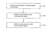
- FIG. 3shows a flow diagram of a method of fabricating a transistor for a memory cell in accordance with an embodiment of the present invention.
- memory soft error ratesare reduced by counter doping the N+/P-well junction of an NMOS transistor.
- the counter-doping implantmay comprise a single implant step.
- the counter doping implantmay also comprise multiple implant steps to prevent excessive increase of junction capacitance, which may result in losing contact to the N-well and degradation of junction breakdown voltage.
- the counter doping implantis performed in conjunction with the source/drain implant.
- the counter doping implantmay be performed right before or after the source/drain implant. As can be appreciated, this allows the counter doping implant to be performed without additional masking steps and without raising significant integration issues.
- a boron P-well implanthas a concentration of about 1 ⁇ 10 17 /cm 3 and an energy of about 100 to 150 KeV (kilo-electron Volts) for the well implant
- an arsenic N-channel implanthas a concentration of about 0.2-3 ⁇ 10 17 /cm ⁇ 3 and an energy of about 60 KeV
- an arsenic source/drain implanthas a concentration of about 5 ⁇ 10 19 /cm 3 and an energy of about 20 to 60 KeV
- the counter doping implant performed after the source/drain implantmay be a boron implant having a concentration of about 5 ⁇ 10 17 /cm 3 and an energy of about 20 to 60 KeV.
- the counter doping implanthelps reduce soft errors by increasing the critical charge by increasing the N+/P-well junction capacitance, and by decreasing the funnel length to decrease the amount of carriers collected by a reversed bias N+/P-well junction.
- FIG. 2is a graphical illustration of doping profiles in accordance with an embodiment of the present invention.
- the doping profilesare for boron and arsenic implants for an NMOS transistor.
- the vertical axisrepresents dopant concentration (in cm ⁇ 3 ), while the horizontal axis represents the depth of the dopant (in ⁇ m) from the surface of the substrate, which is a silicon substrate in this embodiment.
- Plot 203is due to the arsenic source/drain implant (also referred to as “original arsenic” in FIG. 2 ) and plot 202 is due to the boron P-well implant (also referred to as “original boron” in FIG. 2 ).
- the source/drain implant and the P-well implantresult in an N+/P-well junction (also referred to as “original metllaurgical junction in FIG. 2 ) pointed to by text box 204 .
- N+/P-well junctionalso referred to as “original metllaurgical junction in FIG. 2
- both the “original arsenic” and “optimized arsenic”are on the same plot 203 because no arsenic counter doping is performed as this example is for an NMOS transistor. That is, the source/drain implant is the only arsenic or N-type implant in the example of FIG. 2 .
- Plot 205is due to a boron counter doping implant (also referred to as “optimized boron” in FIG. 2 ) and the original boron P-well implant.
- the boron counter dopingresults in a new N+/P-well junction (also labeled as “optimized metallurgical junction in FIG. 2 ) pointed to by text box 206 .
- the boron counter dopingincreased the boron concentration and moved the N+/P-well junction closer to the surface of the silicon substrate.
- the higher doping concentration on both sides of the N+/P-well junction and the shallower metallurgical junctionincrease the N+/P-well junction capacitance.
- the increase in boron doping concentration beneath the N+/P-well junctioneffectively reduces the funnel length of collected carriers.
- Table 1shows the sensitivity of a soft error rate (SER) failure in time (FIT) to various implant options, while Table 2 shows how FIT is improved by changing the junction capacitance and funnel length.
- SERsoft error rate
- FIG. 3shows a flow diagram of a method of fabricating a MOS transistor for a memory cell in accordance with an embodiment of the present invention.
- a dopantis implanted in a substrate (e.g., silicon substrate) to form a well in a transistor region.
- the dopantmay be a P-type dopant, such as boron, to form a P-well in an NMOS transistor region.
- a dopantis implanted in the substrate to form a highly doped region (i.e., P+ or N+ region), such as source/drain regions.
- the dopant for the source/drain implantmay be an N-type dopant, such as arsenic, to form N+ source/drain regions in the NMOS transistor region.
- a counter doping implantis performed in the transistor region.
- the counter doping implantinvolves the implantation of a dopant having a type opposite to that of the source/drain implant.
- the counter doping implantinvolves implantation of a P-type dopant.
- arsenicis implanted in the substrate to create source/drain regions
- a boron counter doping implantis performed.
- the counter doping implantmay comprise one or more implantation steps performed right before or after the source/drain implant to minimize masking steps.
- the counter doping implantmay employ the same mask as the source/drain implant.
- the counter doping implantmay comprise one or more implantation steps that move the metallurgical junction formed by the well implant and source/drain implant closer to the surface of the substrate and/or increase the concentration of the dopant of the well implant.
- the counter doping implantincreases the metallurgical junction capacitance and reduces funnel length to minimize soft errors in a memory cell where the transistor being fabricated is employed.
Landscapes
- Physics & Mathematics (AREA)
- Engineering & Computer Science (AREA)
- High Energy & Nuclear Physics (AREA)
- General Physics & Mathematics (AREA)
- Toxicology (AREA)
- Condensed Matter Physics & Semiconductors (AREA)
- Health & Medical Sciences (AREA)
- Manufacturing & Machinery (AREA)
- Computer Hardware Design (AREA)
- Microelectronics & Electronic Packaging (AREA)
- Power Engineering (AREA)
- Semiconductor Memories (AREA)
- Metal-Oxide And Bipolar Metal-Oxide Semiconductor Integrated Circuits (AREA)
Abstract
Description
| TABLE 1 | ||||||
| N + SD | PMOS | P + SD | ||||
| Implant | counter | P-well | N-well | 2P + SD | Channel | counter |
| Name | Implant | Implant | Implant | Implant | Implant | implant |
| Change | 47.1 | 17.9 | 10.36 | 8.26 | 5.45 | 3.69 |
| of SER | ||||||
| FIT/Mbit | ||||||
| TABLE 2 | ||||
| Process | SER FIT/Mbit | Reduction | Qcrit | |
| Option | control | SER FIT/Mbit | Ratio | increase |
| Junction Cap | 205-211 | W/Options | 4.2x-5.4x | 3% |
| LiCap | 37-47 | 39-48 | 4x-7.5x | 10% |
Claims (10)
Priority Applications (1)
| Application Number | Priority Date | Filing Date | Title |
|---|---|---|---|
| US10/936,275US7268052B1 (en) | 2003-09-24 | 2004-09-08 | Method for reducing soft error rates of memory cells |
Applications Claiming Priority (2)
| Application Number | Priority Date | Filing Date | Title |
|---|---|---|---|
| US50570203P | 2003-09-24 | 2003-09-24 | |
| US10/936,275US7268052B1 (en) | 2003-09-24 | 2004-09-08 | Method for reducing soft error rates of memory cells |
Publications (1)
| Publication Number | Publication Date |
|---|---|
| US7268052B1true US7268052B1 (en) | 2007-09-11 |
Family
ID=38473220
Family Applications (1)
| Application Number | Title | Priority Date | Filing Date |
|---|---|---|---|
| US10/936,275Active2025-11-19US7268052B1 (en) | 2003-09-24 | 2004-09-08 | Method for reducing soft error rates of memory cells |
Country Status (1)
| Country | Link |
|---|---|
| US (1) | US7268052B1 (en) |
Cited By (2)
| Publication number | Priority date | Publication date | Assignee | Title |
|---|---|---|---|---|
| US20070264990A1 (en)* | 2003-03-06 | 2007-11-15 | Droste Scott T | Emergency call-back for a wireless communication device equipped with a user removable module |
| CN111128738A (en)* | 2018-10-31 | 2020-05-08 | 台湾积体电路制造股份有限公司 | Semiconductor device and method of forming the same |
Citations (6)
| Publication number | Priority date | Publication date | Assignee | Title |
|---|---|---|---|---|
| US5013671A (en)* | 1990-06-20 | 1991-05-07 | Texas Instruments Incorporated | Process for reduced emitter-base capacitance in bipolar transistor |
| US5132235A (en)* | 1987-08-07 | 1992-07-21 | Siliconix Incorporated | Method for fabricating a high voltage MOS transistor |
| US5330922A (en)* | 1989-09-25 | 1994-07-19 | Texas Instruments Incorporated | Semiconductor process for manufacturing semiconductor devices with increased operating voltages |
| US6117716A (en)* | 1996-02-15 | 2000-09-12 | Micron Technology, Inc. | Methods of forming BICMOS circuitry |
| US6660605B1 (en)* | 2002-11-12 | 2003-12-09 | Texas Instruments Incorporated | Method to fabricate optimal HDD with dual diffusion process to optimize transistor drive current junction capacitance, tunneling current and channel dopant loss |
| US6670682B1 (en)* | 2002-08-29 | 2003-12-30 | Micron Technology, Inc. | Multilayered doped conductor |
- 2004
- 2004-09-08USUS10/936,275patent/US7268052B1/enactiveActive
Patent Citations (6)
| Publication number | Priority date | Publication date | Assignee | Title |
|---|---|---|---|---|
| US5132235A (en)* | 1987-08-07 | 1992-07-21 | Siliconix Incorporated | Method for fabricating a high voltage MOS transistor |
| US5330922A (en)* | 1989-09-25 | 1994-07-19 | Texas Instruments Incorporated | Semiconductor process for manufacturing semiconductor devices with increased operating voltages |
| US5013671A (en)* | 1990-06-20 | 1991-05-07 | Texas Instruments Incorporated | Process for reduced emitter-base capacitance in bipolar transistor |
| US6117716A (en)* | 1996-02-15 | 2000-09-12 | Micron Technology, Inc. | Methods of forming BICMOS circuitry |
| US6670682B1 (en)* | 2002-08-29 | 2003-12-30 | Micron Technology, Inc. | Multilayered doped conductor |
| US6660605B1 (en)* | 2002-11-12 | 2003-12-09 | Texas Instruments Incorporated | Method to fabricate optimal HDD with dual diffusion process to optimize transistor drive current junction capacitance, tunneling current and channel dopant loss |
Non-Patent Citations (1)
| Title |
|---|
| RAM Reliability: Soft Errors, Apr. 14, 1998, pp. 1-3, [retrieved on Sep. 19, 2003], retrieved from the internet: URL:http://www.crystallineconcepts.com/ram/ram-soft.html/. |
Cited By (4)
| Publication number | Priority date | Publication date | Assignee | Title |
|---|---|---|---|---|
| US20070264990A1 (en)* | 2003-03-06 | 2007-11-15 | Droste Scott T | Emergency call-back for a wireless communication device equipped with a user removable module |
| US7627307B2 (en) | 2003-03-06 | 2009-12-01 | Motorola, Inc. | Emergency call-back for a wireless communication device equipped with a user removable module |
| CN111128738A (en)* | 2018-10-31 | 2020-05-08 | 台湾积体电路制造股份有限公司 | Semiconductor device and method of forming the same |
| CN111128738B (en)* | 2018-10-31 | 2023-04-25 | 台湾积体电路制造股份有限公司 | Semiconductor device and method of forming the same |
Similar Documents
| Publication | Publication Date | Title |
|---|---|---|
| US6348719B1 (en) | Using a change in doping of poly gate to permit placing both high voltage and low voltage transistors on the same chip | |
| US6500705B2 (en) | Semiconductor memory device and method of manufacturing the same | |
| US8421130B2 (en) | Method for manufacturing SRAM devices with reduced threshold voltage deviation | |
| WO2007047429A1 (en) | A cmos device with zero soft error rate | |
| US20120083080A1 (en) | Method for reducing punch-through in a transistor device | |
| US10217838B2 (en) | Semiconductor structure with multiple transistors having various threshold voltages | |
| US4603471A (en) | Method for making a CMOS circuit having a reduced tendency to latch by controlling the band-gap of source and drain regions | |
| US7488653B2 (en) | Semiconductor device and method for implantation of doping agents in a channel | |
| US7105413B2 (en) | Methods for forming super-steep diffusion region profiles in MOS devices and resulting semiconductor topographies | |
| US6528897B2 (en) | Semiconductor memory device | |
| US5950079A (en) | Semiconductor processing methods of forming complementary metal oxide semiconductor memory and other circuitry | |
| US7268052B1 (en) | Method for reducing soft error rates of memory cells | |
| JP2001284540A (en) | Semiconductor device and method of manufacturing the same | |
| US6476430B1 (en) | Integrated circuit | |
| US4728998A (en) | CMOS circuit having a reduced tendency to latch | |
| US20160211346A1 (en) | Epitaxial Channel Transistors and Die With Diffusion Doped Channels | |
| KR20060053174A (en) | Source / Drain Structures for High-Performance 0.1-submicron Transistors | |
| US9922971B2 (en) | Integration of analog transistor | |
| JP4542736B2 (en) | Semiconductor device | |
| EP0650190B1 (en) | Single event upset hardening of commercial VLSI technology without circuit redesign | |
| US20040043571A1 (en) | Buried-channel transistor with reduced leakage current | |
| KR20000041323A (en) | Semiconductor device having triple well construction | |
| JPH0322476A (en) | Semiconductor storage device | |
| JPH0613562A (en) | Method for manufacturing CMOS transistor with increased junction breakdown voltage | |
| KR19990004888A (en) | Fabrication of Semiconductor Devices for Reducing Leakage Current in Most Transistors |
Legal Events
| Date | Code | Title | Description |
|---|---|---|---|
| AS | Assignment | Owner name:CYPRESS SEMICONDUCTOR CORPORATION, CALIFORNIA Free format text:ASSIGNMENT OF ASSIGNORS INTEREST;ASSIGNORS:XU, YANZHONG;POHLAND, OLIVER;REEL/FRAME:015782/0451;SIGNING DATES FROM 20040825 TO 20040903 | |
| STCF | Information on status: patent grant | Free format text:PATENTED CASE | |
| FEPP | Fee payment procedure | Free format text:PAYER NUMBER DE-ASSIGNED (ORIGINAL EVENT CODE: RMPN); ENTITY STATUS OF PATENT OWNER: LARGE ENTITY Free format text:PAYOR NUMBER ASSIGNED (ORIGINAL EVENT CODE: ASPN); ENTITY STATUS OF PATENT OWNER: LARGE ENTITY | |
| FPAY | Fee payment | Year of fee payment:4 | |
| FPAY | Fee payment | Year of fee payment:8 | |
| AS | Assignment | Owner name:MORGAN STANLEY SENIOR FUNDING, INC., NEW YORK Free format text:SECURITY INTEREST;ASSIGNORS:CYPRESS SEMICONDUCTOR CORPORATION;SPANSION LLC;REEL/FRAME:035240/0429 Effective date:20150312 | |
| MAFP | Maintenance fee payment | Free format text:PAYMENT OF MAINTENANCE FEE, 12TH YEAR, LARGE ENTITY (ORIGINAL EVENT CODE: M1553); ENTITY STATUS OF PATENT OWNER: LARGE ENTITY Year of fee payment:12 | |
| AS | Assignment | Owner name:MUFG UNION BANK, N.A., CALIFORNIA Free format text:ASSIGNMENT AND ASSUMPTION OF SECURITY INTEREST IN INTELLECTUAL PROPERTY;ASSIGNOR:MORGAN STANLEY SENIOR FUNDING, INC.;REEL/FRAME:050896/0366 Effective date:20190731 | |
| AS | Assignment | Owner name:MORGAN STANLEY SENIOR FUNDING, INC., NEW YORK Free format text:CORRECTIVE ASSIGNMENT TO CORRECT THE 8647899 PREVIOUSLY RECORDED ON REEL 035240 FRAME 0429. ASSIGNOR(S) HEREBY CONFIRMS THE SECURITY INTERST;ASSIGNORS:CYPRESS SEMICONDUCTOR CORPORATION;SPANSION LLC;REEL/FRAME:058002/0470 Effective date:20150312 | |
| AS | Assignment | Owner name:SPANSION LLC, CALIFORNIA Free format text:RELEASE BY SECURED PARTY;ASSIGNOR:MUFG UNION BANK, N.A.;REEL/FRAME:059410/0438 Effective date:20200416 Owner name:CYPRESS SEMICONDUCTOR CORPORATION, CALIFORNIA Free format text:RELEASE BY SECURED PARTY;ASSIGNOR:MUFG UNION BANK, N.A.;REEL/FRAME:059410/0438 Effective date:20200416 | |
| AS | Assignment | Owner name:INFINEON TECHNOLOGIES LLC, CALIFORNIA Free format text:ASSIGNMENT OF ASSIGNORS INTEREST;ASSIGNOR:CYPRESS SEMICONDUCTOR CORPORATION;REEL/FRAME:059721/0467 Effective date:20200315 |