US7266787B2 - Method for optimising transistor performance in integrated circuits - Google Patents
Method for optimising transistor performance in integrated circuitsDownload PDFInfo
- Publication number
- US7266787B2 US7266787B2US11/067,200US6720005AUS7266787B2US 7266787 B2US7266787 B2US 7266787B2US 6720005 AUS6720005 AUS 6720005AUS 7266787 B2US7266787 B2US 7266787B2
- Authority
- US
- United States
- Prior art keywords
- cell
- cells
- diffusion
- integrated circuit
- active regions
- Prior art date
- Legal status (The legal status is an assumption and is not a legal conclusion. Google has not performed a legal analysis and makes no representation as to the accuracy of the status listed.)
- Expired - Lifetime, expires
Links
Images


Classifications
- H—ELECTRICITY
- H10—SEMICONDUCTOR DEVICES; ELECTRIC SOLID-STATE DEVICES NOT OTHERWISE PROVIDED FOR
- H10D—INORGANIC ELECTRIC SEMICONDUCTOR DEVICES
- H10D89/00—Aspects of integrated devices not covered by groups H10D84/00 - H10D88/00
- H10D89/10—Integrated device layouts
- H—ELECTRICITY
- H10—SEMICONDUCTOR DEVICES; ELECTRIC SOLID-STATE DEVICES NOT OTHERWISE PROVIDED FOR
- H10D—INORGANIC ELECTRIC SEMICONDUCTOR DEVICES
- H10D84/00—Integrated devices formed in or on semiconductor substrates that comprise only semiconducting layers, e.g. on Si wafers or on GaAs-on-Si wafers
- H10D84/90—Masterslice integrated circuits
- H10D84/903—Masterslice integrated circuits comprising field effect technology
- H10D84/907—CMOS gate arrays
Definitions
- This inventionrelates generally to integrated circuits, and more particularly to methods for optimising performance of logic cells within a standard cell library for large scale integration of semiconductor integrated circuits.
- a standard cellis a pre-designed layout of transistors or non-specific collection of logic gates that are typically designed with computer assisted design (CAD) applications.
- CADcomputer assisted design
- the cellsare usually interconnected or wired together in a particular manner with means of a placement and routing tool to perform a specific type of logical operation in an application specific IC (ASIC).
- a conventional ASIC layoutis typically defined by an array of logic cells arranged in adjacent rows. Such a row 10 is shown in FIG. 1 .
- the row of cellsis depicted for illustrative purposes as a layout representation of abutting logic cells 12 , 31 , 32 , 33 , 35 bound by power and ground rails 14 , 16 .
- Each logic celldefines a specific logic circuit.
- the active areas or components of the logic cellinclude negative-channel diffusion 24 , positive-channel diffusion 26 , and gate 34 layers.
- the components of the logic cellsare wired internally with vias 28 and metal layer 18 , 20 , 22 to form simple logic (NMOS and PMOS) gates to perform Boolean and logic functions, for example INVERTER (or NOT) 12 , 35 , AND, OR, NAND 31 , NOR 32 , 33 XOR, XNOR, ADDERS, FLIP-FLOP, and the like.
- integrated circuit design rulesmust be observed, for example, minimum width of transistor width, minimum width of metal tracks, and the like.
- An aspect of the inventionprovides a method for optimising transistor performance in an integrated circuit, comprises providing an integrated circuit having at least two cells, each cell having a logic function defined by the interconnection between active regions, non-active regions and power rails, each cell having an edge defined by a non-active region each cell having a connection between an active diffusion region and a power rail; identifying at least two adjacent cells each having a corresponding connection between an active region to the same power rail; and joining the respective active regions associated with each corresponding connection of each cell with an additional diffusion area across the boundary between the cells forming the connected diffusion of the two adjacent cells.
- An aspect of the inventionprovides a method for building an integrated circuit having a connected diffusion cell architecture, comprises: providing a logic cell library having at least one cell, each cell having a logic function defined by the interconnection between active regions, non-active regions and power rails, each cell having an edge defined by a non-active region, each cell having a connection between an active region and a power rail; placing cells from the logic cell library into the integrated circuit; identifying at least two adjacent cells in the integrated circuit each having a corresponding connection between an active region to the same power rail; and joining the respective active regions associated with each corresponding connection of each cell with an additional diffusion area across the boundary between the cells forming the connected diffusion of the two adjacent cells.
- the active regionscomprise a positive diffusion area, a negative diffusion area and a gate area.
- the connected diffusionmay be the negative diffusion area or wherein each negative diffusion area of each adjacent cell are connected and each positive diffusion area of each adjacent cell are connected.
- the corresponding connectionmay be positioned along the edge of the cell forming a boundary between the two cells and the two corresponding connections. Additionally, an embodiment may further comprise reorientating a cell having a corresponding connection positioned along an edge, the cell being reoriented with the edge having the corresponding connection adjacent to and forming the boundary between the two cells for joining the diffusion areas.
- An aspect of the inventionprovides an integrated circuit having a connected diffusion cell architecture, comprising: at least two adjacent cells, each cell having a logic function defined by the interconnection between active regions, non-active regions and power rails, each cell having an edge defined by a non-active region, each cell having a connection between an active region and a power rail; additional diffusion area across the boundary between the cells joining the respective active diffusion region associated with the corresponding connection of each cell forming the connected diffusion of the two adjacent cells.
- FIG. 1shows a physical layout design of a row of cell structures within a CMOS environment
- FIG. 2shows a physical layout design of cell structures of FIG. 1 reconfigured in accordance with an embodiment of the invention
- FIG. 3Shows a physical layout design of cell structures of FIG. 2 having continuous active areas in accordance with an embodiment of the invention
- FIG. 4A-Bshows a schematic diagram of a side view of NMOS regions of two adjacent cells in accordance with an embodiment of the invention.
- FIG. 5A-Bare flow charts of methods in accordance with an embodiment of the invention.
- a conventional cellincludes non-active areas 36 , for example STI regions, surrounding active areas or regions 24 , 26 , 34 within each cell.
- the STI regions forming cell boundariesstraddle the border of two adjacent cells.
- the active areasinclude the diffusion 24 , 26 and gate areas 34 .
- the supply nets 20 , 18are supply connections between positive-channel 26 and negative-channel diffusion 24 and respective power rails 14 , 16 (V DD ,V SS ).
- the supply netsmay be configured along a boundary or an edge 39 of the cell.
- a boundary or edge 39 of the cellis defined by a continuous STI region 36 that straddles across two adjacent cells, at the block level, between power and ground rails 14 , 16 .
- each cellmay have at least one positive net and/or at least one negative net along an edge. Therefore adjacent cells may or may not have corresponding supply nets along bordering edges.
- FIG. 2shows a layout symbolic representation 70 of the row of logic cells of FIG. 1 , however, cells with corresponding nets along an edge of bordering cells may be flipped about a y-axis (not shown) of the cell.
- the flipped cells 71 , 73 , 75have edges with corresponding positive nets and negative nets of adjacent cells orientated to lie adjacent across the cell boundary of the adjacent cell 78 . It will be appreciated that it may not be necessary to flip any cells, for example, adjacent cells may already have corresponding nets along the boundary 78 .
- FIG. 2shows respective positive and negative net orientation, however, advantages of embodiments of the invention may be achieved with orientating the cells such that only the same net type (i.e. positive nets or alternatively the negative nets) of each adjacent cell lie along the edge of the boundary between the two cells.
- FIG. 3shows the cell row arrangement of FIG. 2 in accordance with an embodiment of the invention the area bound between the corresponding supply nets of the two adjacent cells are filled at the block level above the cells with additional diffusion 102 .
- This filling of diffusionalters the overall diffusion profile of the adjacent cells.
- the two adjacent cells having an edge with corresponding NMOS (V SS ) negative nets that lie on either side of the cell boundaryform a continuous negative-channel diffusion 24 .
- Nets 18 , 20accordingly continue to interconnect diffusions 24 , 26 for each cell. It will be appreciated that the same process may be applied to the positive-channel 26 diffusion.
- the advantages of filling the negative-channel diffusion of NMOSimproves performance, however, the invention is not limited to filling only the negative-channel diffusion.
- the additional diffusion 102may be filled with various techniques known in the field, such as a dummy layer or abutment algorithm method, grow/shrink method, and the like.
- a dummy layer or abutment algorithm methodFor example in the dummy layer approach, each cell is built, or modified such that a dummy mask layer is added in the region between the cell border, and the diffusion which connects to a V SS net. This will have a minimum width of “W”, by virtue of manufacturing design rules.
- Wminimum width of “W”
- the dummy layer widthis equal to “2W”
- the dummy layeris replaced with diffusion fill.
- all NMOS diffusionis grown in the horizontal direction by an amount “W”.
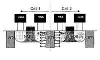
- FIG. 4A-Bshows schematic diagrams of a side view of NMOS regions of two adjacent cells in accordance with an embodiment of the invention.
- FIG. 4Ashows the STI and active regions and the stress resulting from STI being a harder material than the diffusion regions (NMOS or PMOS). The pushing force between the two materials creates stress which impacts the performance.
- the stressis removed, as shown in FIG. 4B . Diffusion may be added where adjacent supply nets connected to the same power or ground.
- the diffusion fillis added between cell 1 and cell 2 at the block level of the IC, which is the next level up in the design hierarchy, above the cell level, and consists of multiple rows of such cells.
- FIG. 5Ashows a flow chart of a method 300 in accordance with an embodiment of the invention.
- a standard cell libraryis provided 310 .
- the ASIC 315is built from a cell, or more typically a collection of cells in the library.
- ASICintegrated circuit
- cellsare interconnected to effect a specific function. Those cells may be arranged in an array of rows.
- two adjacent cellsare identified 320 along the row that have the same net, for example V SS , on diffusion on either side of a boundary between the two cells.
- the diffusion areas associated with the supply nets of the two cellsare joined 330 such that the two adjacent cells that are identified with corresponding nets form a single continuous diffusion area.
- FIG. 5Bshows a flow chart of a method 350 in accordance with another embodiment that shares steps 320 , 330 and may also have the optional flipping step 352 as set out in the method of FIG. 5A .
- the method of FIG. 5Bbegins with having the ASIC provided 305 .
- the active areasi.e. negative and positive diffusion channels 24 , 26 have a longer continuous length than the arrangement of FIG. 1 .
- a longer continuous diffusion channel lengthreduces the number interfaces occurring between active diffusion areas and STI regions along a row of cells. For example, for cells 33 , 35 in FIG. 1 , the number of active diffusion area and STI region interactions is halved as shown in comparing FIGS. 1 and 3 . The reduction in the occurrences of stress between the STI regions and the active diffusion areas correlates with an improvement in performance.
- An embodiment of the inventionmay be implemented with computer aided design (CAD) systems that are well known to a skilled person.
- Well known hardware description languagessuch as Very High Speed Integrated Circuit Hardware Description Language (VHDL) and VERILOG, both international standard languages of Institute of Electrical and Electronic Engineers, Inc. (IEEE), may be used to implement the invention to describe an ASIC, which is then synthesized into detailed logic functions comprising standard cells.
- VHDLVery High Speed Integrated Circuit Hardware Description Language
- IEEEInstitute of Electrical and Electronic Engineers, Inc.
- An example of a tool to perform the synthesisis DESIGN COMPILER (DESIGN COMPILER is a trademark in certain countries of Synopsys, Inc. of Mountain View, Calif., United States of America).
- the cell librarymay also be designed with modelling tools or logic schematic programs on a CAD system to create symbolic representations such as a layout of logic functions, for example, VIRTUOSO (VIRTUOSO is a trademark in certain countries of Cadence Design Systems, Inc., of San Jose, Calif., United States of America).
- VIRTUOSOis a trademark in certain countries of Cadence Design Systems, Inc., of San Jose, Calif., United States of America.
- the ASICmay be built in rows of standard cells as mentioned above, or by other techniques known such as custom transistor level layout or the like.
- ASIC developersmay use “place and route” (P&R) tools to flip the cells as required for increasing the applicability of the technique.
- P&Rplace and route
- the placement and routing toolsgenerate the associated mask patterns to physically wire the standard cells in the manner required to implement the ASIC function.
- placement toolsprovide initial placement of cells in a block or IC when the routing needs are estimated
- routing toolsare capable of moving cells from their initial placement once the routing needs are known.
- place and route toolsexamples include PHYSICAL COMPILER and ASTRO, respectively (PHYSICAL COMPILER and ASTRO are trademarks in certain countries of Synopsys, Inc.).
- PHYSICAL COMPILER and ASTROare trademarks in certain countries of Synopsys, Inc.
- block level diffusion fill methodas described above provides advantages such as limiting the occurrence of stress between active areas and STI regions of the logic cells and improving overall performance. Additionally, embodiments may be applied to all types of ASICS, whether the ASIC is built from a collection of logic cells of a standard cell library (as discussed above) or from other techniques such as from full custom layout and the like. It will be appreciated that specific embodiments of the invention are discussed for illustrative purposes, and various modifications may be made without departing from the scope of the invention as defined by the appended claims.
Landscapes
- Design And Manufacture Of Integrated Circuits (AREA)
- Semiconductor Integrated Circuits (AREA)
Abstract
Description
Claims (38)
Priority Applications (5)
| Application Number | Priority Date | Filing Date | Title |
|---|---|---|---|
| US11/067,200US7266787B2 (en) | 2005-02-24 | 2005-02-24 | Method for optimising transistor performance in integrated circuits |
| JP2007556648AJP5080280B2 (en) | 2005-02-24 | 2006-02-17 | Method for optimizing transistor performance in integrated circuits |
| TW095105363ATWI417936B (en) | 2005-02-24 | 2006-02-17 | Method for optimizing transistor performance in integrated circuits |
| PCT/GB2006/000568WO2006090124A2 (en) | 2005-02-24 | 2006-02-17 | Method for optimizing transistor performance in integrated circuits by diffusion sharing across cell boundaries |
| EP06709805AEP1859373A2 (en) | 2005-02-24 | 2006-02-17 | Method for optimizing transistor performance in integrated circuits by diffusion sharing across cell boundaries |
Applications Claiming Priority (1)
| Application Number | Priority Date | Filing Date | Title |
|---|---|---|---|
| US11/067,200US7266787B2 (en) | 2005-02-24 | 2005-02-24 | Method for optimising transistor performance in integrated circuits |
Publications (2)
| Publication Number | Publication Date |
|---|---|
| US20060186478A1 US20060186478A1 (en) | 2006-08-24 |
| US7266787B2true US7266787B2 (en) | 2007-09-04 |
Family
ID=36586191
Family Applications (1)
| Application Number | Title | Priority Date | Filing Date |
|---|---|---|---|
| US11/067,200Expired - LifetimeUS7266787B2 (en) | 2005-02-24 | 2005-02-24 | Method for optimising transistor performance in integrated circuits |
Country Status (5)
| Country | Link |
|---|---|
| US (1) | US7266787B2 (en) |
| EP (1) | EP1859373A2 (en) |
| JP (1) | JP5080280B2 (en) |
| TW (1) | TWI417936B (en) |
| WO (1) | WO2006090124A2 (en) |
Cited By (40)
| Publication number | Priority date | Publication date | Assignee | Title |
|---|---|---|---|---|
| US20070202663A1 (en)* | 2006-02-27 | 2007-08-30 | Synopsys, Inc. | Managing integrated circuit stress using stress adjustment trenches |
| US20070202652A1 (en)* | 2006-02-27 | 2007-08-30 | Synopsys, Inc. | Elevation of transistor channels to reduce impact of shallow trench isolation on transistor performance |
| US20070204250A1 (en)* | 2006-02-27 | 2007-08-30 | Synopsys, Inc. | Stress-managed revision of integrated circuit layouts |
| US20090007043A1 (en)* | 2006-02-27 | 2009-01-01 | Synopsys, Inc. | Managing Integrated Circuit Stress Using Dummy Diffusion Regions |
| US7620926B1 (en)* | 2007-03-20 | 2009-11-17 | Xilinx, Inc. | Methods and structures for flexible power management in integrated circuits |
| US20100023902A1 (en)* | 2005-12-01 | 2010-01-28 | Synopsys, Inc. | Analysis of stress impact on transistor performance |
| US20100270597A1 (en)* | 2009-04-24 | 2010-10-28 | Synopsys, Inc. | Method and apparatus for placing transistors in proximity to through-silicon vias |
| US20110156101A1 (en)* | 2009-12-28 | 2011-06-30 | Elpida Memory, Inc. | Semiconductor device and layout design apparatus of semiconductor device |
| US20110258588A1 (en)* | 2010-04-19 | 2011-10-20 | Freescale Semiconductor, Inc. | Integrated circuit device with reduced leakage and method therefor |
| US20120240088A1 (en)* | 2011-03-14 | 2012-09-20 | Taiwan Semiconductor Manufacturing Company, Ltd. | Systems and methods of designing integrated circuits |
| US20140159772A1 (en)* | 2006-03-09 | 2014-06-12 | Tela Innovations, Inc. | Circuitry and Layouts for XOR and XNOR Logic |
| US8847324B2 (en) | 2012-12-17 | 2014-09-30 | Synopsys, Inc. | Increasing ION /IOFF ratio in FinFETs and nano-wires |
| US8904322B2 (en)* | 2013-03-26 | 2014-12-02 | International Business Machines Corporation | Structure for stacked CMOS circuits |
| US8921896B2 (en) | 2006-03-09 | 2014-12-30 | Tela Innovations, Inc. | Integrated circuit including linear gate electrode structures having different extension distances beyond contact |
| US8951916B2 (en) | 2007-12-13 | 2015-02-10 | Tela Innovations, Inc. | Super-self-aligned contacts and method for making the same |
| US9009641B2 (en) | 2006-03-09 | 2015-04-14 | Tela Innovations, Inc. | Circuits with linear finfet structures |
| US9035359B2 (en) | 2006-03-09 | 2015-05-19 | Tela Innovations, Inc. | Semiconductor chip including region including linear-shaped conductive structures forming gate electrodes and having electrical connection areas arranged relative to inner region between transistors of different types and associated methods |
| US20150137252A1 (en)* | 2013-11-18 | 2015-05-21 | Sang-hoon BAEK | Layout design system, layout design method, and semiconductor device fabricated by using the same |
| US9081931B2 (en) | 2008-03-13 | 2015-07-14 | Tela Innovations, Inc. | Cross-coupled transistor circuit having diffusion regions of common node on opposing sides of same gate electrode track and gate node connection through single interconnect layer |
| US9122823B2 (en) | 2013-12-20 | 2015-09-01 | International Business Machines Corporation | Stacked multiple-input delay gates |
| US9122832B2 (en) | 2008-08-01 | 2015-09-01 | Tela Innovations, Inc. | Methods for controlling microloading variation in semiconductor wafer layout and fabrication |
| US9159627B2 (en) | 2010-11-12 | 2015-10-13 | Tela Innovations, Inc. | Methods for linewidth modification and apparatus implementing the same |
| US9177894B2 (en) | 2012-08-31 | 2015-11-03 | Synopsys, Inc. | Latch-up suppression and substrate noise coupling reduction through a substrate back-tie for 3D integrated circuits |
| US9202779B2 (en) | 2008-01-31 | 2015-12-01 | Tela Innovations, Inc. | Enforcement of semiconductor structure regularity for localized transistors and interconnect |
| US9230910B2 (en) | 2006-03-09 | 2016-01-05 | Tela Innovations, Inc. | Oversized contacts and vias in layout defined by linearly constrained topology |
| US9240413B2 (en) | 2006-03-09 | 2016-01-19 | Tela Innovations, Inc. | Methods, structures, and designs for self-aligning local interconnects used in integrated circuits |
| US9269702B2 (en) | 2009-10-13 | 2016-02-23 | Tela Innovations, Inc. | Methods for cell boundary encroachment and layouts implementing the same |
| US9312260B2 (en) | 2010-05-26 | 2016-04-12 | Taiwan Semiconductor Manufacturing Company, Ltd. | Integrated circuits and manufacturing methods thereof |
| US9336344B2 (en) | 2006-03-09 | 2016-05-10 | Tela Innovations, Inc. | Coarse grid design methods and structures |
| US9379018B2 (en) | 2012-12-17 | 2016-06-28 | Synopsys, Inc. | Increasing Ion/Ioff ratio in FinFETs and nano-wires |
| US9390215B2 (en) | 2008-03-27 | 2016-07-12 | Tela Innovations, Inc. | Methods for multi-wire routing and apparatus implementing same |
| US9418990B2 (en) | 2014-10-01 | 2016-08-16 | Samsung Electronics Co., Ltd. | Semiconductor device and method of manufacturing the same |
| US9424387B2 (en) | 2007-03-07 | 2016-08-23 | Tela Innovations, Inc. | Methods for cell phasing and placement in dynamic array architecture and implementation of the same |
| US9563733B2 (en) | 2009-05-06 | 2017-02-07 | Tela Innovations, Inc. | Cell circuit and layout with linear finfet structures |
| US9589091B2 (en) | 2006-03-09 | 2017-03-07 | Tela Innovations, Inc. | Scalable meta-data objects |
| US9595515B2 (en) | 2007-03-07 | 2017-03-14 | Tela Innovations, Inc. | Semiconductor chip including integrated circuit defined within dynamic array section |
| US9633987B2 (en) | 2007-03-05 | 2017-04-25 | Tela Innovations, Inc. | Integrated circuit cell library for multiple patterning |
| US9754878B2 (en) | 2006-03-09 | 2017-09-05 | Tela Innovations, Inc. | Semiconductor chip including a chip level based on a layout that includes both regular and irregular wires |
| US9817928B2 (en) | 2012-08-31 | 2017-11-14 | Synopsys, Inc. | Latch-up suppression and substrate noise coupling reduction through a substrate back-tie for 3D integrated circuits |
| US20170344686A1 (en)* | 2016-05-25 | 2017-11-30 | Taiwan Semiconductor Manufacturing Co., Ltd. | Systems and methods for minimum-implant-area aware detailed placement |
Families Citing this family (8)
| Publication number | Priority date | Publication date | Assignee | Title |
|---|---|---|---|---|
| JP5147654B2 (en)* | 2008-11-18 | 2013-02-20 | パナソニック株式会社 | Semiconductor device |
| US8836040B2 (en)* | 2012-11-07 | 2014-09-16 | Qualcomm Incorporated | Shared-diffusion standard cell architecture |
| US9563731B2 (en)* | 2013-03-15 | 2017-02-07 | Taiwan Semiconductor Manufacturing Co., Ltd. | Cell boundaries for self aligned multiple patterning abutments |
| KR102083388B1 (en)* | 2013-09-24 | 2020-03-02 | 삼성전자주식회사 | Semiconductor device and method of forming the same |
| US10366196B2 (en) | 2016-06-22 | 2019-07-30 | Qualcomm Incorporated | Standard cell architecture for diffusion based on fin count |
| US9761712B1 (en)* | 2016-10-31 | 2017-09-12 | International Business Machines Corporation | Vertical transistors with merged active area regions |
| US9978682B1 (en)* | 2017-04-13 | 2018-05-22 | Qualcomm Incorporated | Complementary metal oxide semiconductor (CMOS) standard cell circuits employing metal lines in a first metal layer used for routing, and related methods |
| KR102836167B1 (en)* | 2020-07-14 | 2025-07-21 | 삼성전자주식회사 | Semiconductor device |
Citations (13)
| Publication number | Priority date | Publication date | Assignee | Title |
|---|---|---|---|---|
| US4700316A (en) | 1985-03-01 | 1987-10-13 | International Business Machines Corporation | Automated book layout in static CMOS |
| US5701255A (en) | 1994-09-14 | 1997-12-23 | Matsushita Electric Industrial Co., Ltd. | Cell generation method and cell generation system |
| US6163877A (en) | 1996-11-05 | 2000-12-19 | Intel Corporation | Method and apparatus for optimizing transistor cell layout with integrated transistor folding |
| US6393601B1 (en) | 1997-04-14 | 2002-05-21 | Matsushita Electric Industrial Co., Ltd. | Layout designing apparatus for integrated circuit, transistor size determining apparatus, circuit characteristic evaluating method, and transistor size determining method |
| US6410972B1 (en) | 1999-09-22 | 2002-06-25 | Kabushiki Kaisha Toshiba | Standard cell having a special region and semiconductor integrated circuit containing the standard cells |
| US20020137307A1 (en)* | 2001-03-24 | 2002-09-26 | Kim Chang Gyu | Method for forming isolation layer of semiconductor device |
| US20030023937A1 (en) | 2001-06-01 | 2003-01-30 | Mcmanus Michael J. | Method and apparatus for design of integrated circuits |
| US20040031004A1 (en)* | 2002-08-09 | 2004-02-12 | Keiichi Yoshioka | Semiconductor integrated circuit device and fabrication method thereof |
| US20040060030A1 (en)* | 2002-09-24 | 2004-03-25 | Kazuhiko Fujimoto | Power supply wiring method for semiconductor integrated circuit and semiconductor integrated circuit |
| US20040095797A1 (en)* | 2001-08-08 | 2004-05-20 | Sandisk Corporation | Scalable self-aligned dual floating gate memory cell array and methods of forming the array |
| US20040143797A1 (en)* | 2003-01-17 | 2004-07-22 | Infineon Technologies North America Corp. | 7-Tracks standard cell library |
| US20040168141A1 (en)* | 2001-03-19 | 2004-08-26 | Taiwan Semiconductor Manufacturing Company | Structure of integrated circuit standard cell library for reducing power supply voltage fluctuation |
| US20060003522A1 (en)* | 2004-06-30 | 2006-01-05 | Taiwan Semiconductor Manufacturing Co., Ltd. | Semiconductor device substrate with embedded capacitor |
Family Cites Families (1)
| Publication number | Priority date | Publication date | Assignee | Title |
|---|---|---|---|---|
| JPH0442560A (en)* | 1990-06-08 | 1992-02-13 | Nec Corp | Standard cell |
- 2005
- 2005-02-24USUS11/067,200patent/US7266787B2/ennot_activeExpired - Lifetime
- 2006
- 2006-02-17TWTW095105363Apatent/TWI417936B/enactive
- 2006-02-17EPEP06709805Apatent/EP1859373A2/ennot_activeWithdrawn
- 2006-02-17JPJP2007556648Apatent/JP5080280B2/enactiveActive
- 2006-02-17WOPCT/GB2006/000568patent/WO2006090124A2/enactiveApplication Filing
Patent Citations (14)
| Publication number | Priority date | Publication date | Assignee | Title |
|---|---|---|---|---|
| US4700316A (en) | 1985-03-01 | 1987-10-13 | International Business Machines Corporation | Automated book layout in static CMOS |
| US5701255A (en) | 1994-09-14 | 1997-12-23 | Matsushita Electric Industrial Co., Ltd. | Cell generation method and cell generation system |
| US6163877A (en) | 1996-11-05 | 2000-12-19 | Intel Corporation | Method and apparatus for optimizing transistor cell layout with integrated transistor folding |
| US6393601B1 (en) | 1997-04-14 | 2002-05-21 | Matsushita Electric Industrial Co., Ltd. | Layout designing apparatus for integrated circuit, transistor size determining apparatus, circuit characteristic evaluating method, and transistor size determining method |
| US6410972B1 (en) | 1999-09-22 | 2002-06-25 | Kabushiki Kaisha Toshiba | Standard cell having a special region and semiconductor integrated circuit containing the standard cells |
| US20040168141A1 (en)* | 2001-03-19 | 2004-08-26 | Taiwan Semiconductor Manufacturing Company | Structure of integrated circuit standard cell library for reducing power supply voltage fluctuation |
| US20020137307A1 (en)* | 2001-03-24 | 2002-09-26 | Kim Chang Gyu | Method for forming isolation layer of semiconductor device |
| US20030023937A1 (en) | 2001-06-01 | 2003-01-30 | Mcmanus Michael J. | Method and apparatus for design of integrated circuits |
| US20030023935A1 (en)* | 2001-06-01 | 2003-01-30 | Mcmanus Michael J. | Method and apparatus for integrated circuit design with library cells |
| US20040095797A1 (en)* | 2001-08-08 | 2004-05-20 | Sandisk Corporation | Scalable self-aligned dual floating gate memory cell array and methods of forming the array |
| US20040031004A1 (en)* | 2002-08-09 | 2004-02-12 | Keiichi Yoshioka | Semiconductor integrated circuit device and fabrication method thereof |
| US20040060030A1 (en)* | 2002-09-24 | 2004-03-25 | Kazuhiko Fujimoto | Power supply wiring method for semiconductor integrated circuit and semiconductor integrated circuit |
| US20040143797A1 (en)* | 2003-01-17 | 2004-07-22 | Infineon Technologies North America Corp. | 7-Tracks standard cell library |
| US20060003522A1 (en)* | 2004-06-30 | 2006-01-05 | Taiwan Semiconductor Manufacturing Co., Ltd. | Semiconductor device substrate with embedded capacitor |
Non-Patent Citations (3)
| Title |
|---|
| Gupta A., et al: "Clip: An Optimizing Layout Generator for Two-Dimensional CMOS Cells," Proceedings of the Design Automation Conference. Anaheim, Jun. 9-13, 1997, New York, ACM, US, vol. CONF. 34, Jun. 9, 1997, pp. 452-455. |
| Gupta A., et al: "Near-Optimum Hierarchical Layout Synthesis of Two-Dimensional CMOS Cells," VLSI Design 1999. Proceedings. Twelfth International Conference on Goa, India Jan. 7-10, 1999, Los Alamitos, CA, USA, IEEE Comput. Soc, US, Jan. 7, 1999, pp. 453-459. |
| Krishna B., et al: "Diffusion Sharing Across Cell Boundaries In Cell Based Design," Circuits and Systems, 1996., IEEE 39th Midwest Symposium on Ames, IA, USA Aug. 18-21, 1996, New York, NY, USA, IEEE, US, vol. 1, Aug. 18, 1996, pp. 349-352. |
Cited By (111)
| Publication number | Priority date | Publication date | Assignee | Title |
|---|---|---|---|---|
| US9465897B2 (en) | 2005-12-01 | 2016-10-11 | Synopsys, Inc. | Analysis of stress impact on transistor performance |
| US20100023899A1 (en)* | 2005-12-01 | 2010-01-28 | Synopsys, Inc. | Analysis of stress impact on transistor performance |
| US8615728B2 (en)* | 2005-12-01 | 2013-12-24 | Synopsys, Inc. | Analysis of stress impact on transistor performance |
| US8661398B1 (en) | 2005-12-01 | 2014-02-25 | Synopsys, Inc. | Analysis of stress impact on transistor performance |
| US8881073B1 (en) | 2005-12-01 | 2014-11-04 | Synopsys, Inc. | Analysis of stress impact on transistor performance |
| US8560995B2 (en) | 2005-12-01 | 2013-10-15 | Synopsys, Inc. | Analysis of stress impact on transistor performance |
| US9141737B1 (en) | 2005-12-01 | 2015-09-22 | Synopsys, Inc. | Analysis of stress impact on transistor performance |
| US9189580B1 (en) | 2005-12-01 | 2015-11-17 | Synopsys, Inc. | Analysis of stress impact on transistor performance |
| US20100023902A1 (en)* | 2005-12-01 | 2010-01-28 | Synopsys, Inc. | Analysis of stress impact on transistor performance |
| US20070298566A1 (en)* | 2006-02-27 | 2007-12-27 | Synopsys, Inc. | Elevation of transistor channels to reduce impact of shallow trench isolation on transistor performance |
| US8035168B2 (en) | 2006-02-27 | 2011-10-11 | Synopsys, Inc. | Elevation of transistor channels to reduce impact of shallow trench isolation on transistor performance |
| US7863146B2 (en) | 2006-02-27 | 2011-01-04 | Synopsys, Inc. | Elevation of transistor channels to reduce impact of shallow trench isolation on transistor performance |
| US7897479B2 (en) | 2006-02-27 | 2011-03-01 | Synopsys, Inc. | Managing integrated circuit stress using dummy diffusion regions |
| US20100019317A1 (en)* | 2006-02-27 | 2010-01-28 | Synopsys, Inc. | Managing Integrated Circuit Stress Using Stress Adjustment Trenches |
| US20090313595A1 (en)* | 2006-02-27 | 2009-12-17 | Synopsys, Inc. | Stress-managed revision of integrated circuit layouts |
| US7600207B2 (en) | 2006-02-27 | 2009-10-06 | Synopsys, Inc. | Stress-managed revision of integrated circuit layouts |
| US7767515B2 (en)* | 2006-02-27 | 2010-08-03 | Synopsys, Inc. | Managing integrated circuit stress using stress adjustment trenches |
| US20090007043A1 (en)* | 2006-02-27 | 2009-01-01 | Synopsys, Inc. | Managing Integrated Circuit Stress Using Dummy Diffusion Regions |
| US8069430B2 (en) | 2006-02-27 | 2011-11-29 | Synopsys, Inc. | Stress-managed revision of integrated circuit layouts |
| US20070204250A1 (en)* | 2006-02-27 | 2007-08-30 | Synopsys, Inc. | Stress-managed revision of integrated circuit layouts |
| US8686512B2 (en) | 2006-02-27 | 2014-04-01 | Synopsys, Inc. | Elevation of transistor channels to reduce impact of shallow trench isolation on transistor performance |
| US20070202652A1 (en)* | 2006-02-27 | 2007-08-30 | Synopsys, Inc. | Elevation of transistor channels to reduce impact of shallow trench isolation on transistor performance |
| US20070202663A1 (en)* | 2006-02-27 | 2007-08-30 | Synopsys, Inc. | Managing integrated circuit stress using stress adjustment trenches |
| US9240413B2 (en) | 2006-03-09 | 2016-01-19 | Tela Innovations, Inc. | Methods, structures, and designs for self-aligning local interconnects used in integrated circuits |
| US9035359B2 (en) | 2006-03-09 | 2015-05-19 | Tela Innovations, Inc. | Semiconductor chip including region including linear-shaped conductive structures forming gate electrodes and having electrical connection areas arranged relative to inner region between transistors of different types and associated methods |
| US9425272B2 (en) | 2006-03-09 | 2016-08-23 | Tela Innovations, Inc. | Semiconductor chip including integrated circuit including four transistors of first transistor type and four transistors of second transistor type with electrical connections between various transistors and methods for manufacturing the same |
| US10230377B2 (en) | 2006-03-09 | 2019-03-12 | Tela Innovations, Inc. | Circuitry and layouts for XOR and XNOR logic |
| US10217763B2 (en) | 2006-03-09 | 2019-02-26 | Tela Innovations, Inc. | Semiconductor chip having region including gate electrode features of rectangular shape on gate horizontal grid and first-metal structures of rectangular shape on at least eight first-metal gridlines of first-metal vertical grid |
| US20140159772A1 (en)* | 2006-03-09 | 2014-06-12 | Tela Innovations, Inc. | Circuitry and Layouts for XOR and XNOR Logic |
| US10186523B2 (en) | 2006-03-09 | 2019-01-22 | Tela Innovations, Inc. | Semiconductor chip having region including gate electrode features formed in part from rectangular layout shapes on gate horizontal grid and first-metal structures formed in part from rectangular layout shapes on at least eight first-metal gridlines of first-metal vertical grid |
| US10141334B2 (en) | 2006-03-09 | 2018-11-27 | Tela Innovations, Inc. | Semiconductor chip including region having rectangular-shaped gate structures and first-metal structures |
| US10141335B2 (en) | 2006-03-09 | 2018-11-27 | Tela Innovations, Inc. | Semiconductor CIP including region having rectangular-shaped gate structures and first metal structures |
| US9230910B2 (en) | 2006-03-09 | 2016-01-05 | Tela Innovations, Inc. | Oversized contacts and vias in layout defined by linearly constrained topology |
| US8921896B2 (en) | 2006-03-09 | 2014-12-30 | Tela Innovations, Inc. | Integrated circuit including linear gate electrode structures having different extension distances beyond contact |
| US8921897B2 (en) | 2006-03-09 | 2014-12-30 | Tela Innovations, Inc. | Integrated circuit with gate electrode conductive structures having offset ends |
| US9917056B2 (en) | 2006-03-09 | 2018-03-13 | Tela Innovations, Inc. | Coarse grid design methods and structures |
| US9425145B2 (en) | 2006-03-09 | 2016-08-23 | Tela Innovations, Inc. | Oversized contacts and vias in layout defined by linearly constrained topology |
| US9009641B2 (en) | 2006-03-09 | 2015-04-14 | Tela Innovations, Inc. | Circuits with linear finfet structures |
| US9336344B2 (en) | 2006-03-09 | 2016-05-10 | Tela Innovations, Inc. | Coarse grid design methods and structures |
| US9905576B2 (en) | 2006-03-09 | 2018-02-27 | Tela Innovations, Inc. | Semiconductor chip including region having rectangular-shaped gate structures and first metal structures |
| US9859277B2 (en) | 2006-03-09 | 2018-01-02 | Tela Innovations, Inc. | Methods, structures, and designs for self-aligning local interconnects used in integrated circuits |
| US9754878B2 (en) | 2006-03-09 | 2017-09-05 | Tela Innovations, Inc. | Semiconductor chip including a chip level based on a layout that includes both regular and irregular wires |
| US9741719B2 (en) | 2006-03-09 | 2017-08-22 | Tela Innovations, Inc. | Methods, structures, and designs for self-aligning local interconnects used in integrated circuits |
| US9711495B2 (en) | 2006-03-09 | 2017-07-18 | Tela Innovations, Inc. | Oversized contacts and vias in layout defined by linearly constrained topology |
| US9673825B2 (en)* | 2006-03-09 | 2017-06-06 | Tela Innovations, Inc. | Circuitry and layouts for XOR and XNOR logic |
| US9425273B2 (en) | 2006-03-09 | 2016-08-23 | Tela Innovations, Inc. | Semiconductor chip including integrated circuit including at least five gate level conductive structures having particular spatial and electrical relationship and method for manufacturing the same |
| US9443947B2 (en) | 2006-03-09 | 2016-09-13 | Tela Innovations, Inc. | Semiconductor chip including region having integrated circuit transistor gate electrodes formed by various conductive structures of specified shape and position and method for manufacturing the same |
| US9589091B2 (en) | 2006-03-09 | 2017-03-07 | Tela Innovations, Inc. | Scalable meta-data objects |
| US9633987B2 (en) | 2007-03-05 | 2017-04-25 | Tela Innovations, Inc. | Integrated circuit cell library for multiple patterning |
| US10074640B2 (en) | 2007-03-05 | 2018-09-11 | Tela Innovations, Inc. | Integrated circuit cell library for multiple patterning |
| US9595515B2 (en) | 2007-03-07 | 2017-03-14 | Tela Innovations, Inc. | Semiconductor chip including integrated circuit defined within dynamic array section |
| US9424387B2 (en) | 2007-03-07 | 2016-08-23 | Tela Innovations, Inc. | Methods for cell phasing and placement in dynamic array architecture and implementation of the same |
| US9910950B2 (en) | 2007-03-07 | 2018-03-06 | Tela Innovations, Inc. | Methods for cell phasing and placement in dynamic array architecture and implementation of the same |
| US7620926B1 (en)* | 2007-03-20 | 2009-11-17 | Xilinx, Inc. | Methods and structures for flexible power management in integrated circuits |
| US10734383B2 (en) | 2007-10-26 | 2020-08-04 | Tela Innovations, Inc. | Methods, structures, and designs for self-aligning local interconnects used in integrated circuits |
| US9818747B2 (en) | 2007-12-13 | 2017-11-14 | Tela Innovations, Inc. | Super-self-aligned contacts and method for making the same |
| US10461081B2 (en) | 2007-12-13 | 2019-10-29 | Tel Innovations, Inc. | Super-self-aligned contacts and method for making the same |
| US9281371B2 (en) | 2007-12-13 | 2016-03-08 | Tela Innovations, Inc. | Super-self-aligned contacts and method for making the same |
| US8951916B2 (en) | 2007-12-13 | 2015-02-10 | Tela Innovations, Inc. | Super-self-aligned contacts and method for making the same |
| US9202779B2 (en) | 2008-01-31 | 2015-12-01 | Tela Innovations, Inc. | Enforcement of semiconductor structure regularity for localized transistors and interconnect |
| US9530734B2 (en) | 2008-01-31 | 2016-12-27 | Tela Innovations, Inc. | Enforcement of semiconductor structure regularity for localized transistors and interconnect |
| US9871056B2 (en) | 2008-03-13 | 2018-01-16 | Tela Innovations, Inc. | Semiconductor chip including integrated circuit having cross-coupled transistor configuration and method for manufacturing the same |
| US10727252B2 (en) | 2008-03-13 | 2020-07-28 | Tela Innovations, Inc. | Semiconductor chip including integrated circuit having cross-coupled transistor configuration and method for manufacturing the same |
| US10020321B2 (en) | 2008-03-13 | 2018-07-10 | Tela Innovations, Inc. | Cross-coupled transistor circuit defined on two gate electrode tracks |
| US10651200B2 (en) | 2008-03-13 | 2020-05-12 | Tela Innovations, Inc. | Cross-coupled transistor circuit defined on three gate electrode tracks |
| US9213792B2 (en) | 2008-03-13 | 2015-12-15 | Tela Innovations, Inc. | Semiconductor chip including digital logic circuit including at least six transistors with some transistors forming cross-coupled transistor configuration and associated methods |
| US9208279B2 (en) | 2008-03-13 | 2015-12-08 | Tela Innovations, Inc. | Semiconductor chip including digital logic circuit including linear-shaped conductive structures having electrical connection areas located within inner region between transistors of different type and associated methods |
| US9081931B2 (en) | 2008-03-13 | 2015-07-14 | Tela Innovations, Inc. | Cross-coupled transistor circuit having diffusion regions of common node on opposing sides of same gate electrode track and gate node connection through single interconnect layer |
| US10658385B2 (en) | 2008-03-13 | 2020-05-19 | Tela Innovations, Inc. | Cross-coupled transistor circuit defined on four gate electrode tracks |
| US9117050B2 (en) | 2008-03-13 | 2015-08-25 | Tela Innovations, Inc. | Integrated circuit including cross-coupled transistors having gate electrodes formed within gate level feature layout channels with gate contact position and offset specifications |
| US9245081B2 (en) | 2008-03-13 | 2016-01-26 | Tela Innovations, Inc. | Semiconductor chip including digital logic circuit including at least nine linear-shaped conductive structures collectively forming gate electrodes of at least six transistors with some transistors forming cross-coupled transistor configuration and associated methods |
| US9536899B2 (en) | 2008-03-13 | 2017-01-03 | Tela Innovations, Inc. | Semiconductor chip including integrated circuit having cross-coupled transistor configuration and method for manufacturing the same |
| US9779200B2 (en) | 2008-03-27 | 2017-10-03 | Tela Innovations, Inc. | Methods for multi-wire routing and apparatus implementing same |
| US9390215B2 (en) | 2008-03-27 | 2016-07-12 | Tela Innovations, Inc. | Methods for multi-wire routing and apparatus implementing same |
| US9122832B2 (en) | 2008-08-01 | 2015-09-01 | Tela Innovations, Inc. | Methods for controlling microloading variation in semiconductor wafer layout and fabrication |
| US8362622B2 (en) | 2009-04-24 | 2013-01-29 | Synopsys, Inc. | Method and apparatus for placing transistors in proximity to through-silicon vias |
| US9003348B2 (en) | 2009-04-24 | 2015-04-07 | Synopsys, Inc. | Placing transistors in proximity to through-silicon vias |
| US20100270597A1 (en)* | 2009-04-24 | 2010-10-28 | Synopsys, Inc. | Method and apparatus for placing transistors in proximity to through-silicon vias |
| US9275182B2 (en)* | 2009-04-24 | 2016-03-01 | Synopsys, Inc. | Placing transistors in proximity to through-silicon vias |
| US8661387B2 (en) | 2009-04-24 | 2014-02-25 | Synopsys, Inc. | Placing transistors in proximity to through-silicon vias |
| US9563733B2 (en) | 2009-05-06 | 2017-02-07 | Tela Innovations, Inc. | Cell circuit and layout with linear finfet structures |
| US10446536B2 (en) | 2009-05-06 | 2019-10-15 | Tela Innovations, Inc. | Cell circuit and layout with linear finfet structures |
| US9530795B2 (en) | 2009-10-13 | 2016-12-27 | Tela Innovations, Inc. | Methods for cell boundary encroachment and semiconductor devices implementing the same |
| US9269702B2 (en) | 2009-10-13 | 2016-02-23 | Tela Innovations, Inc. | Methods for cell boundary encroachment and layouts implementing the same |
| US20110156101A1 (en)* | 2009-12-28 | 2011-06-30 | Elpida Memory, Inc. | Semiconductor device and layout design apparatus of semiconductor device |
| US8354696B2 (en)* | 2009-12-28 | 2013-01-15 | Elpida Memory, Inc. | Semiconductor device and layout design apparatus of semiconductor device |
| US20110258588A1 (en)* | 2010-04-19 | 2011-10-20 | Freescale Semiconductor, Inc. | Integrated circuit device with reduced leakage and method therefor |
| US8898614B2 (en)* | 2010-04-19 | 2014-11-25 | Freescale Semiconductor, Inc. | Integrated circuit device with reduced leakage and method therefor |
| US12094880B2 (en) | 2010-05-26 | 2024-09-17 | Taiwan Semiconductor Manufacturing Co., Ltd. | Integrated circuits and manufacturing methods thereof |
| US9312260B2 (en) | 2010-05-26 | 2016-04-12 | Taiwan Semiconductor Manufacturing Company, Ltd. | Integrated circuits and manufacturing methods thereof |
| US10535655B2 (en) | 2010-05-26 | 2020-01-14 | Taiwan Semiconductor Manufacturing Co., Ltd. | Integrated circuits and manufacturing methods thereof |
| US11581314B2 (en) | 2010-05-26 | 2023-02-14 | Taiwan Semiconductor Manufacturing Co., Ltd. | Integrated circuits and manufacturing methods thereof |
| US9704845B2 (en) | 2010-11-12 | 2017-07-11 | Tela Innovations, Inc. | Methods for linewidth modification and apparatus implementing the same |
| US9159627B2 (en) | 2010-11-12 | 2015-10-13 | Tela Innovations, Inc. | Methods for linewidth modification and apparatus implementing the same |
| US8473888B2 (en)* | 2011-03-14 | 2013-06-25 | Taiwan Semiconductor Manufacturing Company, Ltd. | Systems and methods of designing integrated circuits |
| US20120240088A1 (en)* | 2011-03-14 | 2012-09-20 | Taiwan Semiconductor Manufacturing Company, Ltd. | Systems and methods of designing integrated circuits |
| US9817928B2 (en) | 2012-08-31 | 2017-11-14 | Synopsys, Inc. | Latch-up suppression and substrate noise coupling reduction through a substrate back-tie for 3D integrated circuits |
| US9190346B2 (en) | 2012-08-31 | 2015-11-17 | Synopsys, Inc. | Latch-up suppression and substrate noise coupling reduction through a substrate back-tie for 3D integrated circuits |
| US9177894B2 (en) | 2012-08-31 | 2015-11-03 | Synopsys, Inc. | Latch-up suppression and substrate noise coupling reduction through a substrate back-tie for 3D integrated circuits |
| US9184110B2 (en) | 2012-08-31 | 2015-11-10 | Synopsys, Inc. | Latch-up suppression and substrate noise coupling reduction through a substrate back-tie for 3D integrated circuits |
| US9379018B2 (en) | 2012-12-17 | 2016-06-28 | Synopsys, Inc. | Increasing Ion/Ioff ratio in FinFETs and nano-wires |
| US8847324B2 (en) | 2012-12-17 | 2014-09-30 | Synopsys, Inc. | Increasing ION /IOFF ratio in FinFETs and nano-wires |
| US8904322B2 (en)* | 2013-03-26 | 2014-12-02 | International Business Machines Corporation | Structure for stacked CMOS circuits |
| US20150137252A1 (en)* | 2013-11-18 | 2015-05-21 | Sang-hoon BAEK | Layout design system, layout design method, and semiconductor device fabricated by using the same |
| US9633161B2 (en)* | 2013-11-18 | 2017-04-25 | Samsung Electronics Co., Ltd. | Layout design system, method, and semiconductor device employing termination-free unit designs |
| US9122823B2 (en) | 2013-12-20 | 2015-09-01 | International Business Machines Corporation | Stacked multiple-input delay gates |
| US9947661B2 (en) | 2014-10-01 | 2018-04-17 | Samsung Electronics Co., Ltd. | Semiconductor device and method of manufacturing the same |
| US9748238B2 (en) | 2014-10-01 | 2017-08-29 | Samsung Electronics Co., Ltd. | Semiconductor device and method of manufacturing the same |
| US9418990B2 (en) | 2014-10-01 | 2016-08-16 | Samsung Electronics Co., Ltd. | Semiconductor device and method of manufacturing the same |
| US9940424B2 (en)* | 2016-05-25 | 2018-04-10 | Taiwan Semiconductor Manufacturing Co., Ltd. | Systems and methods for minimum-implant-area aware detailed placement |
| US20170344686A1 (en)* | 2016-05-25 | 2017-11-30 | Taiwan Semiconductor Manufacturing Co., Ltd. | Systems and methods for minimum-implant-area aware detailed placement |
Also Published As
| Publication number | Publication date |
|---|---|
| WO2006090124A2 (en) | 2006-08-31 |
| JP2008532275A (en) | 2008-08-14 |
| JP5080280B2 (en) | 2012-11-21 |
| EP1859373A2 (en) | 2007-11-28 |
| TW200710925A (en) | 2007-03-16 |
| US20060186478A1 (en) | 2006-08-24 |
| WO2006090124A3 (en) | 2006-10-12 |
| TWI417936B (en) | 2013-12-01 |
Similar Documents
| Publication | Publication Date | Title |
|---|---|---|
| US7266787B2 (en) | Method for optimising transistor performance in integrated circuits | |
| US20060190893A1 (en) | Logic cell layout architecture with shared boundary | |
| Lopez et al. | A dense gate matrix layout method for MOS VLSI | |
| US8314635B2 (en) | Methods for forming programmable transistor array comprising basic transistor units | |
| JP7668763B2 (en) | METAL ZERO POWER GROUND STUB ROUTE FOR REDUCING CELL AREA AND IMPROVING CELL PLACEMENT AT CHIP LEVEL | |
| US8276109B2 (en) | Mixed-height high speed reduced area cell library | |
| US7287237B2 (en) | Aligned logic cell grid and interconnect routing architecture | |
| US6308309B1 (en) | Place-holding library elements for defining routing paths | |
| Lin | Introduction to VLSI systems: a logic, circuit, and system perspective | |
| Chiluvuri et al. | Layout-synthesis techniques for yield enhancement | |
| US8230380B2 (en) | High speed reduced area cell library with cells having integer multiple track heights | |
| CN112331634B (en) | Metal Oxide Semiconductor MOS Devices | |
| JPH0766943B2 (en) | Integrated circuit and layout method thereof | |
| Kim et al. | Design quality trade-off studies for 3-D ICs built with sub-micron TSVs and future devices | |
| US7062739B2 (en) | Gate reuse methodology for diffused cell-based IP blocks in platform-based silicon products | |
| US7725870B2 (en) | Method for radiation tolerance by implant well notching | |
| Lopez et al. | A dense gate matrix layout method for MOS VLSI | |
| Sherlekar | Design considerations for regular fabrics | |
| Lewis | Optimization of device area and overall delay for CMOS VLSI designs | |
| US20240234322A1 (en) | Semiconductor integrated circuit device | |
| TWI771698B (en) | Multiplexer circuit, multiplexer and method for manufacturing multiplexer | |
| Van Noije et al. | Advanced CMOS gate array architecture combininggate isolation'and programmable routing channels | |
| Ku et al. | Transistor-level monolithic 3D standard cell layout optimization for full-chip static power integrity | |
| Kaur et al. | Power estimation analysis for CMOS cell structures | |
| Moraes et al. | An Efficient Layout Style for Three-Metal CMOS Macro-Cells |
Legal Events
| Date | Code | Title | Description |
|---|---|---|---|
| AS | Assignment | Owner name:ICERA INC., UNITED KINGDOM Free format text:ASSIGNMENT OF ASSIGNORS INTEREST;ASSIGNORS:HUGHES, PETER WILLIAM;MORTON, SHANNON VANCE;MONK, TREVOR KENNETH;REEL/FRAME:016248/0680 Effective date:20050427 | |
| STCF | Information on status: patent grant | Free format text:PATENTED CASE | |
| AS | Assignment | Owner name:ETV CAPITAL SA, LUXEMBOURG Free format text:SECURITY AGREEMENT;ASSIGNOR:ICERA, INC.;REEL/FRAME:021510/0707 Effective date:20080829 Owner name:ETV CAPITAL SA,LUXEMBOURG Free format text:SECURITY AGREEMENT;ASSIGNOR:ICERA, INC.;REEL/FRAME:021510/0707 Effective date:20080829 | |
| AS | Assignment | Owner name:SILICON VALLEY BANK, MASSACHUSETTS Free format text:SECURITY AGREEMENT;ASSIGNOR:ICERA INC.;REEL/FRAME:025387/0659 Effective date:20101122 | |
| FPAY | Fee payment | Year of fee payment:4 | |
| FPAY | Fee payment | Year of fee payment:8 | |
| MAFP | Maintenance fee payment | Free format text:PAYMENT OF MAINTENANCE FEE, 12TH YEAR, LARGE ENTITY (ORIGINAL EVENT CODE: M1553); ENTITY STATUS OF PATENT OWNER: LARGE ENTITY Year of fee payment:12 |