US7266159B2 - Frequency-dependent magnitude pre-distortion on non-baseband input signals for reducing spurious emissions in communication networks - Google Patents
Frequency-dependent magnitude pre-distortion on non-baseband input signals for reducing spurious emissions in communication networksDownload PDFInfo
- Publication number
- US7266159B2 US7266159B2US10/153,289US15328902AUS7266159B2US 7266159 B2US7266159 B2US 7266159B2US 15328902 AUS15328902 AUS 15328902AUS 7266159 B2US7266159 B2US 7266159B2
- Authority
- US
- United States
- Prior art keywords
- baseband
- signal
- distortion
- generate
- input signal
- Prior art date
- Legal status (The legal status is an assumption and is not a legal conclusion. Google has not performed a legal analysis and makes no representation as to the accuracy of the status listed.)
- Expired - Fee Related, expires
Links
Images


Classifications
- H—ELECTRICITY
- H03—ELECTRONIC CIRCUITRY
- H03F—AMPLIFIERS
- H03F1/00—Details of amplifiers with only discharge tubes, only semiconductor devices or only unspecified devices as amplifying elements
- H03F1/32—Modifications of amplifiers to reduce non-linear distortion
- H03F1/3241—Modifications of amplifiers to reduce non-linear distortion using predistortion circuits
- H03F1/3247—Modifications of amplifiers to reduce non-linear distortion using predistortion circuits using feedback acting on predistortion circuits
- H—ELECTRICITY
- H03—ELECTRONIC CIRCUITRY
- H03F—AMPLIFIERS
- H03F1/00—Details of amplifiers with only discharge tubes, only semiconductor devices or only unspecified devices as amplifying elements
- H03F1/32—Modifications of amplifiers to reduce non-linear distortion
- H03F1/3241—Modifications of amplifiers to reduce non-linear distortion using predistortion circuits
- H03F1/3294—Acting on the real and imaginary components of the input signal
- H—ELECTRICITY
- H04—ELECTRIC COMMUNICATION TECHNIQUE
- H04L—TRANSMISSION OF DIGITAL INFORMATION, e.g. TELEGRAPHIC COMMUNICATION
- H04L25/00—Baseband systems
- H04L25/02—Details ; arrangements for supplying electrical power along data transmission lines
- H04L25/03—Shaping networks in transmitter or receiver, e.g. adaptive shaping networks
- H04L25/03828—Arrangements for spectral shaping; Arrangements for providing signals with specified spectral properties
- H04L25/03834—Arrangements for spectral shaping; Arrangements for providing signals with specified spectral properties using pulse shaping
- H—ELECTRICITY
- H04—ELECTRIC COMMUNICATION TECHNIQUE
- H04L—TRANSMISSION OF DIGITAL INFORMATION, e.g. TELEGRAPHIC COMMUNICATION
- H04L27/00—Modulated-carrier systems
- H04L27/32—Carrier systems characterised by combinations of two or more of the types covered by groups H04L27/02, H04L27/10, H04L27/18 or H04L27/26
- H04L27/34—Amplitude- and phase-modulated carrier systems, e.g. quadrature-amplitude modulated carrier systems
- H04L27/36—Modulator circuits; Transmitter circuits
- H04L27/366—Arrangements for compensating undesirable properties of the transmission path between the modulator and the demodulator
- H04L27/367—Arrangements for compensating undesirable properties of the transmission path between the modulator and the demodulator using predistortion
- H04L27/368—Arrangements for compensating undesirable properties of the transmission path between the modulator and the demodulator using predistortion adaptive predistortion
- H—ELECTRICITY
- H03—ELECTRONIC CIRCUITRY
- H03F—AMPLIFIERS
- H03F2200/00—Indexing scheme relating to amplifiers
- H03F2200/102—A non-specified detector of a signal envelope being used in an amplifying circuit
Definitions
- the present inventionrelates to signal processing, and, in particular, to the pre-distortion of signals for transmission, for example, in a wireless communication network, to reduce spurious emissions.
- Modern wireless communication networksemploy complex modulation schemes that necessitate tight control of spurious emissions (sometimes called “out-of-band emissions”) in order to avoid interfering with neighboring carriers and to comply with the requirements of regulatory bodies (e.g., FCC) and standards bodies (e.g. ITU).
- spurious emissionsis the base station transmitter amplifier that is used to amplify signals prior to transmission as wireless (e.g., RF) signals to wireless (e.g., mobile) units in a wireless communication network, such as a cellular voice and/or data network.
- wireless communication networksuch as a cellular voice and/or data network.
- Prior art techniques for reducing such spurious emissionswere able to satisfy previous requirements.
- wireless communication networkse.g., Universal Mobile Telecommunication Service (UMTS)
- UMTSUniversal Mobile Telecommunication Service
- Embodiments of the present inventionare directed to techniques that reduce spurious emissions in wireless communication networks to levels that satisfy current requirements.
- embodiments of the present inventioninvolve pre-distortion, whose magnitude—and preferably phase—are frequency-dependent, that is applied to an input signal to generate a pre-distorted signal that, when applied to an amplifier, results in lower spurious emissions in the resulting amplified signal.
- the present inventionis a method for reducing spurious emissions in an amplified non-baseband signal, comprising the steps of (a) receiving a non-baseband input signal; and (b) applying pre-distortion, whose magnitude is frequency-dependent, to the non-baseband input signal to generate a pre-distorted non-baseband signal, such that, when the pre-distorted non-baseband signal is applied to an amplifier to generate the amplified non-baseband signal, the pre-distortion reduces spurious emissions in the amplified non-baseband signal.
- FIG. 1shows a block diagram of a system, in accordance with the (frequency-independent) pre-distortion technique described in the U.S. patent application Ser. No. 09/395,490;
- FIG. 2shows a block diagram of the digital pre-distorter of FIG. 1 ;
- FIG. 3shows a block diagram of an exemplary FPGA implementation of the index calculating module, the delay block, the look-up table, and the output module of FIG. 2 ;
- FIG. 4shows a block diagram of an exemplary single-channel, single-conversion implementation of the receiver of FIG. 1 ;
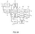
- FIG. 5shows a block diagram of one possible baseband-domain implementation of a pre-distorter having a pre-distortion component whose magnitude and phase are frequency-dependent in conjunction with the frequency-independent pre-distortion component described in the '490 application;
- FIG. 5Ashows a block diagram of a hardware implementation similar to that of FIG. 5 , except that the order of the complex multiplication and differentiation steps in the secondary signal processing path is reversed;
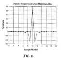
- FIG. 6shows the impulse response of a linear magnitude filter for the differentiating filter for the pre-distorter of FIG. 5 ;
- FIG. 7shows the impulse response of a Hilbert transform filter for the differentiating filter for the pre-distorter of FIG. 5 ;
- FIG. 8shows the impulse response of a single-filter implementation of the differentiating filter for the pre-distorter of FIG. 5 ;
- FIG. 9shows a block diagram of one possible RF-domain implementation of a pre-distorter having a pre-distortion component whose magnitude and phase are frequency-dependent in conjunction with a frequency-independent pre-distortion component;
- FIG. 9Ashows a block diagram of a hardware implementation similar to that of FIG. 9 , except that the order of the complex multiplication and differentiation steps in the secondary signal processing path is reversed.
- the '490 applicationdescribes a technique for reducing spurious emissions using digital pre-distortion that was sufficient to meet previously existing regulations and standards.
- pre-distortionwhose magnitude and phase are frequency-independent, is applied to an input signal to generate a (main) pre-distorted signal that reduces spurious emissions when the pre-distorted signal is subsequently amplified by an amplifier.
- pre-distortionwhose magnitude—and preferably phase—are frequency-dependent, is applied to generate an additional (i.e., secondary) pre-distortion signal that, when combined with the main pre-distorted signal described in the '490 application, can further reduce spurious emissions in the amplified signal.
- pre-distortion techniquetaught in the '490 application. Following that is a description of different possible implementations of a pre-distortion component, whose magnitude and phase are frequency-dependent, that is preferably combined with—but does not necessarily have to be combined with—the pre-distortion technique of the '490 application to further reduce spurious emissions in communications networks.
- the pre-distortion technique described in the '490 applicationreduces adjacent channel power in wireless communication networks.
- the '490 applicationdescribes a technique for digitally and adaptively pre-distorting an outgoing signal that involves applying a correction to the signal before it is applied, e.g., to the input of a base station transmitter amplifier, such that the correction is equal and opposite to at least some of the anticipated distortion produced by the amplifier.
- the correctioncauses at least some of the amplifier distortion to be canceled, resulting in a base station transmitter having a more linear transfer characteristic than a corresponding transmitter without such pre-distortion.
- the adjacent channel poweri.e., spurious emission
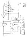
- FIG. 1shows a block diagram of a system 10 , in accordance with the pre-distortion technique described in the '490 application.
- System 10includes a digital pre-distorter 12 for receiving the in-phase (I) and quadrature (Q) components of an input digital baseband signal, an IQ modulator 14 connected to the output of pre-distorter 12 , an amplifier 16 connected to the output of modulator 14 , and a receiver 18 that is coupled to the output of amplifier 16 through a coupler 17 in order to generate a control signal that is fed back to pre-distorter 12 .
- Iin-phase
- Qquadrature
- These componentsare configured to apply a correction to the input digital baseband signal (e.g., a code division multiple access (CDMA) signal, a wide-band CDMA signal, a time division multiple access (TDMA) signal, an enhanced data rates through global system for mobile communications evolution (EDGE) signal, or other signal, preferably with a substantially large peak power to average power ratio) generated by a communication device—such as a base station used for transmitting wireless communication data—and applied to pre-distorter 12 as the input signal (I, Q).
- a communication devicesuch as a base station used for transmitting wireless communication data
- EDGEenhanced data rates through global system for mobile communications evolution
- System 10also provides adaptive feedback through receiver 18 to optimize the correction.
- this pre-distortion techniquecomprises applying a correction to a digital baseband signal before the signal is applied to an input of amplifier 16 such that the correction is opposite to at least a portion of the distortion produced by amplifier 16 .
- the correction and some portion of the amplifier distortioncancel one another, resulting in a system with a more linear transfer characteristic.
- digital pre-distorter 12in order to take advantage of the precision and low cost of digital circuits, digital pre-distorter 12 preferably performs its correction at baseband, before the signal is converted by modulator 14 to radio frequency (RF) for amplification and transmission.
- RFradio frequency
- pre-distorter 12pre-distorts both the magnitude and the phase of the input signal as a function of the signal power (but independent of frequency). Since both the magnitude and phase corrections vary with the instantaneous power (i.e., envelope power), pre-distorter 12 relies on accurate descriptions of the amplifier magnitude and phase variations with power level to perform its function. As will be described below, the functional representation of the corrections (versus power level) are in the form of polynomial equations from which a look-up table is preferably derived.
- the digital baseband signalis comprised of discrete time samples of in-phase (I) and quadrature (Q) components which, after digital-to-analog conversion (not shown), are applied to the vector IQ modulator 14 to generate an RF signal that is then input to amplifier 16 .
- Each sample for the baseband signalcan be represented in complex number notation as (I+jQ), where j is the square root of ( ⁇ 1).
- different values for parameters A and Bmay be stored in a look-up table (which is generated as described below) with the index being the instantaneous envelope power given by (I 2 +Q 2 ).
- FIG. 2shows a block diagram of digital pre-distorter 12 of FIG. 1 , in accordance with the pre-distortion technique of the '490 application.
- pre-distorter 12includes an equalization filter 20 for receiving the signal that is comprised of the in-phase and quadrature components described above.
- the equalization filteris a component that is well known in the art and is operatively connected to a clipping module 22 that clips the signal to a predetermined threshold.
- the output of clipping module 22is fed to a low-pass filter 24 that eliminates the high-frequency components that are generated during clipping.
- the output of low-pass filter 24is fed to a sampling module 26 that provides an up-sampled signal (e.g., increases the sampling rate by a factor of four from an original 2 ⁇ rate to an 8 ⁇ rate) to an index calculating module 28 , which calculates an index value based on the sum of the squares of the in-phase and quadrature components of the baseband signal.
- Index calculating module 28is connected to a look-up table 30 having stored therein parameters A and B. Values for parameters A and B are retrieved based on the calculated index value.
- the pre-distortion parameters A and B of look-up table 30are derived from a set of polynomial equations that closely approximate the corrections used to linearize the amplifier characteristics. Because of the complex nature of the characteristics of amplifiers, such as class AB amplifiers, advantageous results are obtained by using a pair of polynomial equations for parameter B, while a single polynomial equation is sufficient for parameter A.
- a mis a maximum value imposed on parameter A to prevent the amplifier from being driven deep into saturation.
- a typical value for A mis 2, but it can vary depending on the detailed design.
- P bis a breakpoint where parameter B transitions between Equations (6) and (7).
- P bis an optimizable parameter whose value is obtained by the optimization algorithm. The value varies from amplifier to amplifier. It can also vary with temperature.
- C 0 through C 9are coefficients that pertain to the transfer function characteristics of a particular amplifier and which can vary with temperature, aging of the amplifier components, etc. As with P b , the optimization algorithm finds values for coefficients C 0 through C 9 that give optimized results.
- a maximum limit A mcan be placed on the value of parameter A. Also, if necessary, the breakpoint P b where the transition is made from one polynomial equation to the other can have a different value for the A equations than for the B equations.
- an adaptive schemeis employed in this pre-distortion technique whereby the values of the coefficients are at least intermittently optimized (or operated on) to maintain minimum or reduced spurious emissions.
- coupler 17 at the output of amplifier 16samples the output and receiver 18 , which is tuned to the frequency region where the spurious emissions are to be reduced or minimized, generates a voltage proportional to the received power.
- Multiple receiverscan be used to sample the spurious emissions at more than one frequency or a single receiver can tune sequentially to the different frequencies of interest. The voltages obtained at the different frequencies are then combined into a single quantity whose value is to be reduced or minimized.
- Such use of an absolute valuecauses both V 1 and V 2 to be reduced or minimized, instead of simply providing the sum of the two values. If only the first two terms on the right-hand side of Equation (8) were used, the algorithm might find a false optimum by making one voltage very small and the other quite large.
- processing module 32implements the modified simplex algorithm to update the values of parameters A and B stored in look-up table 30 .
- processing module 32may take a variety of forms such as a microprocessor, a digital signal processor, or a processing circuit using FPGA devices.
- the simplex algorithmmay be implemented in any suitable manner that utilizes appropriate combinations of hardware and software that will be apparent to those of skill in the art upon a reading hereof.
- the device used to implement the algorithmhere, module 32
- the values of the coefficients derived by the algorithmare used in the equations for A and B described above to generate a table which is used by the algorithm for the next iteration.
- the algorithmis allowed to run continuously, or at least intermittently, so that the coefficient values track changes that occur over time.
- the simplex optimization algorithm as developed by Nelder and Meadwas intended for minimizing or reducing function values, which were obtained by mathematical computations.
- An important aspect of this mode of operationis that, if a computation is repeated, the same function value is obtained. This contrasts with values obtained by measurements on operating hardware where noise and fluctuations inevitably result in varying measured values. This difference has an important consequence when an attempt is made to use the simplex algorithm in real time on operating hardware.
- the essence of the simplex algorithmis that, at each iteration, the set of coefficients that is associated with the worst function value is replaced with a new set which gives a better function value.
- This new valuemight or might not be better than the best function value obtained up to that time, but as the algorithm progresses it is expected that better and better function values will be obtained.
- an exceptionally good but erroneous valueis obtained. If subsequent values obtained are all worse than this erroneous value, then the algorithm will converge on the erroneous value.
- the algorithmis not very suitable for use in situations where considerable fluctuations exist in the quantity being optimized or operated on as may be in the present case.
- the simplex algorithmis used in modified form. At the end of each iteration, if the previous best value is replaced by a better value, then the algorithm proceeds to the next iteration. However, if an iteration does not yield a new best value, then the existing best point is re-evaluated and the new value is substituted for the previous one. Thus, the algorithm is able to recover from erroneous data due to fluctuating measurements. These fluctuations may result in a larger number of iterations in order to reach a desired point (which could be an optimum point), but will not prevent the desired point from being reached.
- Another modification of the simplex algorithmenables it to operate continuously to track changes in amplifier characteristics caused by temperature changes, aging of components, or other disturbances.
- an exit criterionis established (the criterion is usually related to the fractional variation of the function values between the worst and best points of the simplex) and the algorithm terminates when the criterion is satisfied.
- the algorithmreduces the size of the simplex which typically becomes very small by the time the desired point is reached. Once this happens, the algorithm is no longer able to react to changes in amplifier characteristics.
- the size of the simplexis prevented from becoming too small by comparing it to a value, such as a preset minimum value, at the start of each iteration and increasing the size to the value if it has been reduced below it.
- the valueis chosen such that it is large enough to enable the algorithm to track changes in the amplifier characteristics but not so large that the desired (or optimum) point cannot be reached.
- a suitable valueis one where the value of each coefficient at the worst point of the simplex differs from the corresponding value at the best point by 5 to 10 percent.
- the output of sampling module 26is also connected to a delay circuit 34 , which is, in turn, connected to an output module 36 that generates an output signal based on the values of parameters A and B retrieved from look-up table 30 and the delayed upsampled signal from delay circuit 34 .
- the delay applied by delay circuit 34is preferably equivalent to the delay involved in performing the processing of modules 28 and 30 so that the appropriate values of (I and Q) and (A and B) arrive at output module 36 at the same time.
- FIG. 3shows a block diagram of an exemplary FPGA implementation 300 of index calculating module 28 , delay 34 , look-up table 30 , and output module 36 of FIG. 2 .
- the I and Q data pathsare independently squared at multipliers 302 and 304 to create I 2 and Q 2 , respectively. These two values are added together at adder block 306 to form an index address for look-up table 30 , which, in FIG. 3 , takes the form of two separate dual-port RAM memory blocks 308 and 310 , which contain the parameters A and B, respectively.
- the parameters output from the memory blocksare multiplied by the delayed I and Q values at multipliers 312 , 314 , 316 , and 318 to create the four values I ⁇ A, I ⁇ B, Q ⁇ A, and Q ⁇ B. These are combined by adder and subtractor blocks 320 and 322 to form (IA ⁇ QB) and (QA+IB), respectively, which are output as I′ and Q′.
- Additional circuitry 324loads the dual-port memory blocks 308 and 310 with parameter data generated in processing module 32 using standard memory interface signals.
- the use of dual-port memorypermits real-time updating of the look-up tables without disrupting the accessing of parameter values by the pre-distortion process.
- a look-up table configurationis not necessary where, for example, the processing module has a sufficiently high processing speed to allow for the obtaining of the A and B parameters on an “as needed” basis.
- the processing modulecalculates the appropriate coefficients and the A and B parameters are subsequently calculated by the processing module as needed or desired without storing such parameters in a look-up table.
- receiver 18 in the digital pre-distortion adaptive feedback loopis used to measure the RF power over a narrow bandwidth at a specific frequency.
- This tuned frequencyis offset from, for example, the main CDMA carrier frequency and is a frequency where the spurious emissions are to be minimized by the optimization algorithm.
- FIG. 4shows a block diagram of an exemplary single-channel, single-conversion implementation of receiver 18 of FIG. 1 .
- receiver 18includes a frequency synthesizer 50 , which is connected to a mixer 52 .
- the output of mixer 52is connected to a low-pass filter 54 , which in turn is connected to an intermediate frequency (IF) chain 56 .
- the output of IF chain 56is connected to an analog-to-digital converter (ADC) 58 , which then provides input to processing module 32 of FIG. 2 .
- ADCanalog-to-digital converter
- Three important frequencies in FIG. 4are the RF frequency where the adjacent power level is to be measured, the local oscillator (LO) frequency which is varied as needed to tune the receiver, and intermediate frequency (IF) which is fixed.
- the RF input of receiver 18is coupled off the output of power amplifier 16 by coupler 17 .
- the LO frequency for mixer 52is generated by a phase-locked loop (PLL) frequency synthesizer 50 .
- This LO frequencyis set by (digital) tuning commands from a microprocessor (e.g., processing module 32 of FIG. 2 ).
- Low-pass filter 54is used to filter the RF+LO frequency products, as well as the RF and LO feed-through, and any higher frequency products produced by mixer 52 .
- the receiver IF chain 56is shown as a single block in FIG. 4 .
- IF chain 56actually includes amplifiers and a narrow bandpass filter, which assures that the power being measured is truly the power at the tuned frequency and does not contain power from, for example, the main CDMA carrier.
- IF chain 56produces a Received Signal Strength Indicator (RSSI) voltage output that is proportional to the IF power, which in turn is proportional to the RF power.
- the RSSI voltageis sampled by ADC 58 , where the resulting digitized RSSI is a digital word (which represents the power level at the tuned frequency) that is used by the optimization algorithm implemented by processing module 32 of FIG. 2 .
- the optimization algorithmmonitors the spurious emissions at multiple frequency points, in which case, the single-channel receiver of FIG. 4 may be re-tuned for each different frequency. This re-tuning can be done with a procedure similar to the following:
- the pre-distortion technique of the '490 applicationwas designed to correct for at least some of the non-linearities of the amplifier by pre-distorting both the magnitude of the baseband signal (primarily achieved using the parameter A) as well as the phase (primarily achieved using the parameter B).
- the characteristics of the signalratio of peak power to average power close to 1, as in a single-channel TDMA system
- substantial improvementcan be obtained by correcting the phase as much as possible (via the parameter B) and correcting the magnitude partially by appropriate setting of the A m value.
- the pre-distortion technique of the '490 applicationcan be used to achieve a substantial reduction in spurious emissions, but it is frequently observed that some residual spurious emissions are still present. Attempts to reduce these residual spurious emissions by modifying the coefficients in Equations (4) to (7) (or in Equation (4′) to (7′)) result in an asymmetrical situation where a reduction in the spurious emissions on the low-frequency side of a communication channel are accompanied by an increase in the spurious emissions on the high-frequency side of the channel, and vice-versa, resulting in an overall degradation—or at least no overall improvement—in performance.
- pre-distortionin order to reduce the spurious emissions to a level lower than that achieved by the (frequency-independent) pre-distortion technique of the '490 application, pre-distortion, whose magnitude and phase are frequency-dependent, is also applied.
- the distortion caused by an amplifiercan be considered to be made up of two parts.
- the first partwhich is independent of the signal bandwidth and which is addressed by the '490 application (and other conventional frequency-independent pre-distortion techniques), is associated with the curvature of the amplifier's transfer function which leads to AM-AM (amplitude to amplitude) and AM-PM (amplitude to phase) type of distortions.
- the pre-distortion of the '490 applicationeffectively deals with this part of the amplifier's distortion by correcting the curvature of the transfer function.
- the second part of the amplifier distortionis negligible for narrow bandwidth signals, but it becomes increasingly important as the bandwidth increases.
- This part of the amplifier distortionhas a magnitude that is proportional to the frequency offset from the carrier frequency and a phase shift of ⁇ 90° on either side of the carrier frequency. Since these characteristics match those of a differentiator, a thorough correction of this part of the amplifier's distortion can be achieved using a differentiating filter circuit.
- I and Qare the in-phase and quadrature components of the input signal before pre-distortion
- I′ and Q′are the corresponding components after pre-distortion
- jis the square root of ⁇ 1
- the symbol d/dtrepresents differentiation with respect to time.
- Equation (9)The first term on the right hand side of Equation (9) represents the bandwidth-independent part of the pre-distortion, while the second term represents the bandwidth-dependent part.
- the derivativescan be approximated as follows: d ( I d ) /dt ⁇ I d / ⁇ t, d ( Q d ) /dt ⁇ Q d / ⁇ t (11) for time increments ⁇ t much smaller than the reciprocal of the signal bandwidth.
- Equation (12)The power-independent term a 0 , is in Equation (12), because the output of the first term on the right hand side of Equation (9) (i.e., the main pre-distortion signal) contains the original input signal as well as a pre-distortion signal, but an analogous term does not appear in Equation (14), because the output of the second term on the right hand side of Equation (9) (i.e., the secondary pre-distortion signal) is a pre-distortion signal only.
- FIG. 5shows a block diagram of a hardware (e.g., FPGA, ASIC, or DSP) implementation in which a secondary pre-distortion signal, whose magnitude and phase are frequency-dependent, is combined with the main pre-distortion signal generated in accordance with the '490 application.
- index calculating module 28 , look-up table 30 , delay 34 , and output module 36 of pre-distorter 12 of FIG. 2are shown as being part of the configuration of FIG. 5 that generates the first term on the right-hand side of Equation (9) (i.e., the main pre-distortion signal I 0 , Q 0 ).
- Equation (9)i.e., the main pre-distortion signal I 0 , Q 0 .
- look-up table 502retains values for the parameters X and Y that are accessed based on the index generated by module 28 and then used by complex multiplication module 504 and differentiating filter 506 to calculate the second term on the right-hand side of Equation (9) (i.e., the secondary pre-distortion signal I 1 , Q 1 ).
- Delay block 34compensates for the time required to compute the value of (I 2 +Q 2 ) by module 28 and retrieve values of A, B, X, and Y from look-up tables 30 and 502 .
- the output of module 36is further delayed by delay block 508 to compensate for the time required by differentiating filter 506 to convert the output of module 504 into the secondary pre-distortion signal (i.e., the time to compute the time derivatives of I d and Q d as in Equation (10)).
- the main pre-distortion signal (I 0 , Q 0 )is then combined with the secondary pre-distortion signal (I 1 , Q 1 ) in combiner module 510 to generate the new, combined pre-distorted signal (I′, Q′), which may then be modulated and amplified (e.g., by modulator 14 and amplifier 16 of FIG. 1 ) for transmission.
- both sets of polynomial equations for A and B and for X and Yare shown implemented as pre-computed look-up tables (i.e., 30 and 502 ).
- look-up table 30 and/or look-up table 502can be replaced by real-time computations based on the polynomials in Equations (12)-(15). In either case, depending on the application, the “infinitely long” polynomials in Equations (12)-(15) can be approximated by ignoring higher-order terms.
- Equations (12) and (13)are approximated by ignoring all terms higher than the third-order terms, while Equations (14) and (15) are approximated by ignoring all terms higher than the first-order terms.
- the coefficients used to generate A and Bthe coefficients used to generate X and Y may be generated and adaptively updated using the simplex algorithm.
- the differentiation operation of filter 506can be implemented in a variety of ways.
- the characteristics of a differentiatornamely a magnitude which is proportional to the frequency offset from the carrier and a phase shift of ⁇ 90° on either side of the carrier frequency
- a cascadei.e., a series combination
- two filterseach of which is either an FIR or IIR (infinite impulse response) filter, where one filter is a linear magnitude filter having constant delay and a magnitude response that is proportional to frequency and the other filter is a Hilbert transform filter (with the sign of the coefficients reversed to conform to the definition of a differentiator) whose magnitude response is constant with frequency and whose phase response is 90° at all frequencies (in addition to a constant delay).
- FIG. 6 and 7show representative impulse responses of a linear magnitude FIR filter and a Hilbert transform FIR filter, respectively, that can be combined to form differentiating filter 506 .
- differentiating filter 506can be implemented with the linear magnitude filter before or after the Hilbert transform filter.
- the desired characteristicscan be obtained using a single filter with some compromise in the accuracy of the linear magnitude and the 90° phase shift.
- FIG. 8shows a representative impulse response of a single differentiating FIR filter.
- the sampling frequency of this single filtercan be, but does not have to be much higher than the signal bandwidth.
- the filter coefficients of Equation (17)results in a simple implementation that yields excellent results provided the sampling frequency is at least eight times the signal bandwidth.
- Using a cascade of two filtersprovides more flexibility, since the two filters can be tailored to create a magnitude and phase response that matches that of the amplifier in the event the amplifier has a magnitude response that is not linear and/or a phase response that is not 90° or that varies with frequency (in which case, a Hilbert transform filter would not be used).
- FIG. 5Ashows a block diagram of a hardware implementation similar to that of FIG. 5 , except that the order of the complex multiplication and differentiation steps in the secondary signal processing path is reversed.
- differentiating filter 506 ais placed before complex multiplication block 504 a .
- this implementationincludes an additional delay block 512 .
- the address pointer into lookup table 502 awould be expected to be (i 2 +q 2 ) as derived from the values i and q generated by differentiating filter 506 a .
- FIGS. 5 and 5Aare designed to operate in the baseband domain for situations where the baseband signals I and Q are available. When the baseband signals are not readily available, it may be advantageous to apply pre-distortion to the input signal in a non-baseband domain, such as the RF or IF domain.
- FIG. 9shows a block diagram of a possible RF-domain hardware implementation of a pre-distorter. There is a general one-to-one correspondence between modules in the RF implementation of FIG. 9 and the modules in the baseband implementation of FIG. 5 .
- the RF input signalis split into two paths, one of which goes to envelope detector 902 , which produces an output signal proportional to the instantaneous envelope power of the RF input signal.
- envelope detector 902which produces an output signal proportional to the instantaneous envelope power of the RF input signal.
- This signalis digitized by ADC 904 , whose digital output is used to fetch a pair of control signal values (e.g., voltages V 01 and V 02 ) from look-up table 906 .
- the pair of control signalsis applied to vector modulator 910 , whose function is to modify the magnitude and phase of the RF signal in accordance with the control signals.
- the second RF input signal pathgoes to delay element 908 (e.g., a length of coaxial cable), which causes the RF signal to arrive at vector modulator 910 at the same time as the control signals V 01 and V 02 .
- delay element 908e.g., a length of coaxial cable
- compensationcan be, but does not have to be provided for attenuation in delay element 908 .
- the output of vector modulator 910is delayed by delay element 912 to generate the main RF pre-distortion signal analogous to I 0 , Q 0 in FIG. 5 .
- ADC 904The output of ADC 904 is split into two digital signal paths corresponding to look-up tables 906 and 914 , and the output of delay element 908 is split into two RF signal paths corresponding to vector modulators 910 and 916 .
- Look-up table 914 , vector modulator 916 , and differentiating circuit 918provide the secondary RF pre-distortion signal analogous to I 1 , Q 1 in FIG. 5 .
- look-up table 914 and vector modulator 916implement the term (I+jQ)(X+jY) on the right hand side of Equation (9).
- differentiating circuit 918is implemented using a splitter 922 , a delay element 924 , an attenuator 926 , and a combiner 928 , which together implement the differentiation operation with respect to time using the approximation of Equation (18) (division by 2 is not required because the values in look-up table 914 can be adjusted appropriately).
- Splitter 922splits the RF signal generated by vector modulator 916 into two RF signal paths, one of which is applied to delay element 924 , which delays the RF signal, and the other to attenuator 926 , which attenuates the RF signal to compensate for the attenuation of delay element 924 .
- Combiner 928combines the RF signals from delay element 924 and attenuator 926 to generate the secondary pre-distortion signal.
- Splitter 922 and combiner 928are designed to impart a 180° rotation between the two RF signals so that the delayed signal from delay element 924 is subtracted from the attenuated signal from attenuator 926 .
- Such a rotationcan be achieved by using a 90° splitter and a 90° combiner.
- a 0° splitter and a 180° combiner, or vice-versa, or any other suitable combination of a splitter and a combiner,can be used.
- the delay introduced by delay element 912is one half that introduced by delay element 924 , thus positioning the output of vector modulator 910 half way in time between the two signals at the inputs of combiner 928 .
- the delay introduced by delay element 924should be much smaller than the reciprocal of the signal bandwidth. A value equal to or less than one fifth of the reciprocal of the signal bandwidth gives excellent results.
- Vector modulator 910is configured such that, in the absence of control signal inputs, the RF signal passes through without (or with minimal) distortion, whereas vector modulator 916 is configured such that, in the absence of control signal inputs, little or no RF signal passes through.
- vector modulator 910produces the original RF signal plus a pre-distortion signal
- vector modulator 916produces essentially a pre-distortion signal only.
- the main pre-distortion signal from delay element 912 and the secondary pre-distortion signal from combiner 928are combined together by an RF combiner 920 , where the combined signal constitutes the pre-distorted RF output signal that is applied to the amplifier.
- the input signalis pre-distorted in the RF domain
- a modulator similar to IQ modulator 14 of FIG. 1may be omitted.
- a mixerwould be needed to convert the resulting pre-distorted IF signal to the RF domain prior to being applied to the amplifier.
- the parameters A and B, and X and Yare shown implemented as look-up tables. Alternatively, they can be evaluated in real time by computing the values of the polynomials in Equations (12) to (15). In either case, the coefficients used to generate A, B, X, and Y may be generated and adaptively updated using the simplex algorithm.
- FIG. 9Ashows a block diagram of a hardware implementation similar to that of FIG. 9 , except that the order of the complex multiplication and differentiation steps in the secondary signal processing path is reversed.
- differentiating circuit 918 ais placed before vector modulator 916 a .
- this implementationincludes an additional delay block 930 .
- the index value generated by ADC 904is used to access values for parameters V 11 and V 12 from lookup table 914 a.
- FIGS. 5 , 5 A, 9 , and 9 Acan be implemented in the context of circuitry that includes modules analogous to equalization filter 20 , clipping module 22 , low-pass filter 24 , and sampling module 26 of FIG. 2 .
- one or more—and even all—of these componentsmay be omitted and/or one or more other processing components may be included, depending on the characteristics of the input signals and the requirements of the particular communication network.
- the present inventionhas been described in the context of configurations in which frequency-dependent magnitude and phase pre-distortion of the present invention is combined with the (frequency-independent) magnitude and phase pre-distortion of the '490 application, the present invention is not so limited. In particular, it is possible to perform frequency-dependent magnitude and phase pre-distortion of the present invention without performing the pre-distortion of the '490 application. In that case, the configuration shown in FIG. 5 , for example, could be modified by omitting look-up table 30 and output module 36 and passing a copy of the delayed input signal from delay block 34 directly to delay block 508 , while retaining the processing of look-up table 502 and module 504 .
- frequency-dependent magnitude pre-distortionwithout implementing frequency-dependent phase pre-distortion, with or without the frequency-independent pre-distortion of the '490 application.
- the configuration shown in FIG. 5could be modified such that filter 506 is implemented using only a linear magnitude filter, as in FIG. 6 .
- the present inventionhas been described in the context of wireless signals transmitted from a base station to one or more mobile units of a wireless communication network, the present invention is not so limited. In theory, embodiments of the present invention could be implemented for wireless signals transmitted from a mobile unit to one or more base stations. The present invention can also be implemented in the context of other wireless and even wired communication networks to reduce spurious emissions.
- Embodiments of the present inventionmay be implemented as circuit-based processes, including possible implementation on a single integrated circuit.
- various functions of circuit elementsmay also be implemented as processing steps in a software program.
- Such softwaremay be employed in, for example, a digital signal processor, micro-controller, or general-purpose computer.
- the present inventioncan be embodied in the form of methods and apparatuses for practicing those methods.
- the present inventioncan also be embodied in the form of program code embodied in tangible media, such as floppy diskettes, CD-ROMs, hard drives, or any other machine-readable storage medium, wherein, when the program code is loaded into and executed by a machine, such as a computer, the machine becomes an apparatus for practicing the invention.
- the present inventioncan also be embodied in the form of program code, for example, whether stored in a storage medium, loaded into and/or executed by a machine, or transmitted over some transmission medium or carrier, such as over electrical wiring or cabling, through fiber optics, or via electromagnetic radiation, wherein, when the program code is loaded into and executed by a machine, such as a computer, the machine becomes an apparatus for practicing the invention.
- program codeWhen implemented on a general-purpose processor, the program code segments combine with the processor to provide a unique device that operates analogously to specific logic circuits.
Landscapes
- Engineering & Computer Science (AREA)
- Physics & Mathematics (AREA)
- Power Engineering (AREA)
- Nonlinear Science (AREA)
- Computer Networks & Wireless Communication (AREA)
- Signal Processing (AREA)
- Spectroscopy & Molecular Physics (AREA)
- Amplifiers (AREA)
Abstract
Description
I′+jQ′=(I+jQ)(A+jB) (1)
where
I′=IA−QB (2)
Q′=QA+IB (3)
where I′ and Q′ are the pre-distorted in-phase and quadrature baseband signals generated by pre-distorter12, and A and B are pre-distortion parameters that are a function of the instantaneous envelope power of the input signal represented by I and Q. Conveniently, different values for parameters A and B may be stored in a look-up table (which is generated as described below) with the index being the instantaneous envelope power given by (I2+Q2).
A=C0+C1P+C2P2+C3P3forA≦Am (4)
A=Amotherwise (5)
B=C4P+C5P2+C6P3forP≦Pb (6)
B=(Bb1−Bb2)+C7P+C8P2+C9P3forP>Pb (7)
where P=(I2+Q2) is the instantaneous envelope power. Amis a maximum value imposed on parameter A to prevent the amplifier from being driven deep into saturation. A typical value for Amis 2, but it can vary depending on the detailed design. Pbis a breakpoint where parameter B transitions between Equations (6) and (7). Pbis an optimizable parameter whose value is obtained by the optimization algorithm. The value varies from amplifier to amplifier. It can also vary with temperature. Bb1and Bb2are the values of parameter B at P=Pbusing Equations (6) and (7), respectively. The first term on the right-hand side of Equation (7) is intended to make Equations (6) and (7) continuous at P=Pb. C0through C9are coefficients that pertain to the transfer function characteristics of a particular amplifier and which can vary with temperature, aging of the amplifier components, etc. As with Pb, the optimization algorithm finds values for coefficients C0through C9that give optimized results.
A=C0+C1PforP≦Pb (4′)
A=(Ab1−Ab2)+C2P+C3P2+C4P3forP>Pb (5′)
B=C5P for P≦Pb (6′)
B=(Bb1−Bb2)+C6P+C7P2+C8P3forP>Pb (7′)
where Ab1and Ab2are the values of parameter A at P=Pbusing Equations (4′) and (5′), respectively. As before, a maximum limit Amcan be placed on the value of parameter A. Also, if necessary, the breakpoint Pbwhere the transition is made from one polynomial equation to the other can have a different value for the A equations than for the B equations.
V=V1+V2+|(V1−V2)| (8)
where |(V1−V2)| is the absolute value of (V1−V2). Such use of an absolute value causes both V1and V2to be reduced or minimized, instead of simply providing the sum of the two values. If only the first two terms on the right-hand side of Equation (8) were used, the algorithm might find a false optimum by making one voltage very small and the other quite large. An alternative to Equation (8) is V=max (V1, V2), where max means choose the larger of the values.
- A microprocessor (e.g., processing module32) sends a tuning command to the frequency synthesizer to set the LO frequency (and therefore the receiver's tuned frequency).
- The microprocessor waits for the PLL and RSSI to settle.
- The digitized RSSI value is read by the microprocessor. Multiple readings could be taken if an average RSSI is used.
- These steps are repeated for the next frequency.
I′+jQ′=(I+jQ)(A+jB)+d{(I+jQ)(X+jY)}/dt (9)
where I and Q are the in-phase and quadrature components of the input signal before pre-distortion, I′ and Q′ are the corresponding components after pre-distortion, j is the square root of −1, and A, B, X, and Y, which are functions of the instantaneous power P (P=I2+Q2), are pre-distortion parameters. The symbol d/dt represents differentiation with respect to time. The first term on the right hand side of Equation (9) represents the bandwidth-independent part of the pre-distortion, while the second term represents the bandwidth-dependent part. The second term can be expanded into Equation (10) as follows:
d{(I+jQ)(X+jY)}/dt=d(Id+jQd)/dt=d(Id)/dt+jd(Qd)/dt, (10)
where (Id+jQd)=(I+jQ)(X+jY). Furthermore, the derivatives can be approximated as follows:
d(Id)/dt≈δId/δt, d(Qd)/dt≈δQd/δt (11)
for time increments δt much smaller than the reciprocal of the signal bandwidth.
A=a0+a1P+a2P2+a3P3+ (12)
B=b1P+b2P2+b3P3+ (13)
X=x1P+x2P2+x3P3+ (14)
Y=y1P+y2P2+y3P3+ (15)
Note that a term independent of P appears in Equation (12), but it does not appear in Equation (14). The power-independent term a0, is in Equation (12), because the output of the first term on the right hand side of Equation (9) (i.e., the main pre-distortion signal) contains the original input signal as well as a pre-distortion signal, but an analogous term does not appear in Equation (14), because the output of the second term on the right hand side of Equation (9) (i.e., the secondary pre-distortion signal) is a pre-distortion signal only.
Frequency-Dependent Magnitude and Phase Pre-Distortion in the Baseband Domain
(δId)n={(Id)n+1−(Id)n−1}/2, (δQd)n={(Qd)n+1−(Qd)n−1}/2, (16)
where the subscript outside the parentheses refers to the sample number. This approximation is valid provided the sampling frequency is much greater than the signal bandwidth. Division by δt is not necessary, since this division would introduce a scaling factor that can be incorporated into the look-up table or the polynomials for X and Y.
[c1, c2, c3]=[0.5, 0, −0.5] (17)
δ(Id+jQd)t={(Id+jQd)t+δt−(Id+jQd)t−δt}/2, (18)
where the subscripts indicate the time relationship of the waveforms. Division by δt is not necessary, since this division would introduce a scaling factor that can be incorporated into the look-up table or the polynomials for X and Y.
Claims (20)
Priority Applications (3)
| Application Number | Priority Date | Filing Date | Title |
|---|---|---|---|
| US10/153,289US7266159B2 (en) | 2002-03-08 | 2002-05-22 | Frequency-dependent magnitude pre-distortion on non-baseband input signals for reducing spurious emissions in communication networks |
| PCT/US2003/006321WO2003077495A1 (en) | 2002-03-08 | 2003-03-03 | Frequency-dependent magnitude pre-distortion of non-baseband input signals for reducing spurious emissions in communication networks |
| AU2003213654AAU2003213654A1 (en) | 2002-03-08 | 2003-03-03 | Frequency-dependent magnitude pre-distortion of non-baseband input signals for reducing spurious emissions in communication networks |
Applications Claiming Priority (3)
| Application Number | Priority Date | Filing Date | Title |
|---|---|---|---|
| US36266002P | 2002-03-08 | 2002-03-08 | |
| US36739902P | 2002-03-25 | 2002-03-25 | |
| US10/153,289US7266159B2 (en) | 2002-03-08 | 2002-05-22 | Frequency-dependent magnitude pre-distortion on non-baseband input signals for reducing spurious emissions in communication networks |
Publications (2)
| Publication Number | Publication Date |
|---|---|
| US20030169829A1 US20030169829A1 (en) | 2003-09-11 |
| US7266159B2true US7266159B2 (en) | 2007-09-04 |
Family
ID=27792119
Family Applications (1)
| Application Number | Title | Priority Date | Filing Date |
|---|---|---|---|
| US10/153,289Expired - Fee RelatedUS7266159B2 (en) | 2002-03-08 | 2002-05-22 | Frequency-dependent magnitude pre-distortion on non-baseband input signals for reducing spurious emissions in communication networks |
Country Status (3)
| Country | Link |
|---|---|
| US (1) | US7266159B2 (en) |
| AU (1) | AU2003213654A1 (en) |
| WO (1) | WO2003077495A1 (en) |
Cited By (9)
| Publication number | Priority date | Publication date | Assignee | Title |
|---|---|---|---|---|
| US20060067426A1 (en)* | 2004-09-28 | 2006-03-30 | Maltsev Alexander A | Multicarrier transmitter and methods for generating multicarrier communication signals with power amplifier predistortion and linearization |
| US20070036251A1 (en)* | 2005-08-11 | 2007-02-15 | Siemens Aktiengesellschaft | Method and system for clipping a baseband input signal |
| US20070253510A1 (en)* | 2004-06-21 | 2007-11-01 | Rohde & Schwartz Gmbh & Co. Kg | Method and Device for the Compensation of Signal Errors in Iq-Modulators |
| US20090290880A1 (en)* | 2008-05-20 | 2009-11-26 | Harmonic, Inc. | Dispersion Compensation Circuitry and System for Analog Video Transmission With Direct Modulated Laser |
| US7653147B2 (en)* | 2005-08-17 | 2010-01-26 | Intel Corporation | Transmitter control |
| US20100105349A1 (en)* | 2006-07-11 | 2010-04-29 | Xuecheng Qian | Rf signal sampling apparatus and method |
| US8204456B2 (en) | 2010-09-15 | 2012-06-19 | Fujitsu Semiconductor Limited | Systems and methods for spurious emission cancellation |
| US20120294343A1 (en)* | 2011-05-16 | 2012-11-22 | Phase Matrix, Inc. | RF I/Q Modulator with Sampling Calibration System |
| US9853664B2 (en)* | 2014-06-17 | 2017-12-26 | Huawei Technologies Co., Ltd. | Radio frequency power amplification system, radio frequency power amplification method, transmitter, and base station |
Families Citing this family (8)
| Publication number | Priority date | Publication date | Assignee | Title |
|---|---|---|---|---|
| US7197085B1 (en) | 2002-03-08 | 2007-03-27 | Andrew Corporation | Frequency-dependent magnitude pre-distortion for reducing spurious emissions in communication networks |
| US7193462B2 (en)* | 2005-03-22 | 2007-03-20 | Powerwave Technologies, Inc. | RF power amplifier system employing an analog predistortion module using zero crossings |
| US8489047B2 (en) | 2010-11-02 | 2013-07-16 | Crestcom, Inc. | Transmitter linearized using bias deviation gain adjustment and method therefor |
| US8615208B2 (en) | 2010-11-02 | 2013-12-24 | Crestcom, Inc. | Transmitter linearized in response to signal magnitude derivative parameter and method therefor |
| US8995520B2 (en)* | 2011-02-14 | 2015-03-31 | Fujitsu Limited | Analog continuous-time phase equalizer for data transmission |
| US20130128931A1 (en)* | 2011-11-17 | 2013-05-23 | Aviacomm Inc. | On-chip radio calibration |
| US8611459B2 (en) | 2012-02-29 | 2013-12-17 | Crestcom, Inc. | Transmitter linearized using look-up table with unadaptable data and method therefor |
| US11477060B2 (en)* | 2019-04-16 | 2022-10-18 | Motorola Solutions, Inc. | Systems and methods for modulation classification of baseband signals using attention-based learned filters |
Citations (68)
| Publication number | Priority date | Publication date | Assignee | Title |
|---|---|---|---|---|
| US4870371A (en) | 1986-05-02 | 1989-09-26 | Rohde & Schwarz Gmbh & Co. Kg | Network for cascade compensation of the non-linearity of an amplifier |
| US4890300A (en) | 1987-04-28 | 1989-12-26 | Racal Communications Equipment Limited | Radio transmitters |
| EP0416622A2 (en) | 1989-09-07 | 1991-03-13 | Ortel Corporation | Predistorter for linearization of electronic and optical signals |
| US5132639A (en)* | 1989-09-07 | 1992-07-21 | Ortel Corporation | Predistorter for linearization of electronic and optical signals |
| US5187719A (en) | 1989-01-13 | 1993-02-16 | Hewlett-Packard Company | Method and apparatus for measuring modulation accuracy |
| US5361156A (en)* | 1991-12-09 | 1994-11-01 | Scientific-Atlanta, Inc. | Method and apparatus for predistortion |
| US5872814A (en) | 1997-02-24 | 1999-02-16 | At&T Wireless Services Inc. | Method for linearization of RF transmission electronics using baseband pre-distortion in T/R compensation pilot signals |
| US5937011A (en) | 1996-03-26 | 1999-08-10 | Airnet Communications Corp. | Multi-carrier high power amplifier using digital pre-distortion |
| US6075411A (en) | 1997-12-22 | 2000-06-13 | Telefonaktiebolaget Lm Ericsson | Method and apparatus for wideband predistortion linearization |
| US6081158A (en) | 1997-06-30 | 2000-06-27 | Harris Corporation | Adaptive pre-distortion apparatus for linearizing an amplifier output within a data transmission system |
| US6091941A (en) | 1995-09-19 | 2000-07-18 | Fujitsu Limited | Radio apparatus |
| US6112062A (en) | 1997-09-26 | 2000-08-29 | The Whitaker Corporation | Predistortion for high power amplifiers |
| GB2348755A (en) | 1999-04-01 | 2000-10-11 | Wireless Systems Int Ltd | A digital polynomial predistortion arrangement |
| US6141390A (en) | 1997-05-05 | 2000-10-31 | Glenayre Electronics, Inc. | Predistortion in a linear transmitter using orthogonal kernels |
| US6166603A (en) | 1998-12-02 | 2000-12-26 | Maxim Integrated Products, Inc. | Class-ab output stages with improved distortion performance |
| US6194942B1 (en)* | 2000-01-19 | 2001-02-27 | Cable Vision Electronics Co., Ltd. | Predistortion circuit for linearization of signals |
| EP1085668A2 (en) | 1999-09-14 | 2001-03-21 | Lucent Technologies Inc. | A method and apparatus for reducing adjacent channel power in wireless communication systems |
| US6236267B1 (en) | 1998-12-29 | 2001-05-22 | International Business Machines Corporation | Linearization for power amplifiers using feed-forward and feedback control |
| US6271724B1 (en) | 1997-10-29 | 2001-08-07 | Nokia Networks Oy | Linearization method and amplifier arrangement |
| US6275103B1 (en) | 1998-09-02 | 2001-08-14 | Fujitsu Limited | Predistorter of amplifier and amplifying unit |
| US6281747B2 (en) | 1999-03-09 | 2001-08-28 | Tripath Technology, Inc. | Power efficient line driver |
| US6288814B1 (en) | 1994-05-19 | 2001-09-11 | Ortel Corporation | In-line predistorter for linearization of electronic and optical signals |
| US6288610B1 (en) | 1998-03-19 | 2001-09-11 | Fujitsu Limited | Method and apparatus for correcting signals, apparatus for compensating for distortion, apparatus for preparing distortion compensating data, and transmitter |
| US6304140B1 (en) | 2000-06-12 | 2001-10-16 | Motorola, Inc. | Digital predistortion for amplifiers |
| US20010033238A1 (en) | 1999-04-16 | 2001-10-25 | Velazquez Scott R. | Linearity error compensator |
| US6342810B1 (en) | 1999-07-13 | 2002-01-29 | Pmc-Sierra, Inc. | Predistortion amplifier system with separately controllable amplifiers |
| US6366177B1 (en) | 2000-02-02 | 2002-04-02 | Tropian Inc. | High-efficiency power modulators |
| US20020041210A1 (en) | 2000-05-11 | 2002-04-11 | Andrew Booth | Linear amplifier arrangement |
| US6373902B1 (en) | 1997-06-19 | 2002-04-16 | Samsung Electronics Co., Ltd | Device and method for linearizing transmitter in digital communication system |
| EP1199797A1 (en) | 2000-10-11 | 2002-04-24 | Telefonaktiebolaget Lm Ericsson | Method and apparatus for reducing distortion |
| US20020060606A1 (en) | 2000-10-12 | 2002-05-23 | Tore Andre | Method and apparatus for reducing distortion |
| US20020065048A1 (en) | 1999-07-28 | 2002-05-30 | Kazuo Nagatani | Method and apparatus for compensating for distortion in radio apparatus |
| US6400415B1 (en) | 1997-04-04 | 2002-06-04 | Harris Corporation | System and method for predistorting signals to be amplified |
| US20020080891A1 (en) | 2000-12-27 | 2002-06-27 | Lg Electronics | Base station transmitter having digital predistorter and predistortion method thereof |
| US20020085647A1 (en) | 1999-07-28 | 2002-07-04 | Yasuyuki Oishi | Radio apparatus having distortion compensating function |
| US6417731B1 (en) | 2000-09-22 | 2002-07-09 | Hitachi Kokusai Electric Inc. | Distortion-compensated amplifier device |
| US6429736B1 (en) | 1999-04-23 | 2002-08-06 | Securicor Wireless Technology Limited | On-line calibration of linear amplifiers |
| US6438186B1 (en) | 1998-08-31 | 2002-08-20 | 3Com Corporation | Carrier phase derived symbol timing |
| US20020125947A1 (en) | 2001-03-09 | 2002-09-12 | Qiming Ren | Linearizer for a power amplifier |
| US20020171485A1 (en)* | 2001-05-18 | 2002-11-21 | Spectrian Corporation | Digitally implemented predistorter control mechanism for linearizing high efficiency RF power amplifiers |
| US6489846B2 (en)* | 2000-05-25 | 2002-12-03 | Sony Corporation | Distortion compensating device and distortion compensating method |
| US20020186783A1 (en) | 2001-06-07 | 2002-12-12 | Motorola, Inc | Amplifier predistortion system and method |
| US20030016741A1 (en) | 2001-03-20 | 2003-01-23 | Nir Sasson | Method and system for digital equalization of non-linear distortion |
| EP1280273A2 (en) | 1999-07-13 | 2003-01-29 | PMC-Sierra, Inc. | A wideband digital predistortion linearizer for nonlinear amplifiers |
| US20030020538A1 (en) | 2001-06-07 | 2003-01-30 | Jaehyeong Kim | Method and apparatus for modeling and estimating the characteristics of a power amplifier by retaining even-order terms in estimating characteristics |
| US20030045264A1 (en) | 2001-08-29 | 2003-03-06 | Jeong Hei-Sam | Adaptive linearization technique for communication building block |
| US20030058960A1 (en) | 2001-09-21 | 2003-03-27 | Lg Electronics Inc. | Predistortion type-linearized power amplification system using digital if technology |
| US20030076896A1 (en) | 2000-01-13 | 2003-04-24 | Carsten Ball | Method and apparatus for the linearization of a radio frequency high-power amplifier |
| US20030076894A1 (en) | 1999-08-05 | 2003-04-24 | Hang Jin | Adaptive digital pre-distortion circuit using adjacent channel power profile and method of operation |
| US20030117215A1 (en)* | 2001-12-26 | 2003-06-26 | O'flaherty Martin J. | Methods of optimising power amplifier efficiency and closed-loop power amplifier controllers |
| US6587514B1 (en) | 1999-07-13 | 2003-07-01 | Pmc-Sierra, Inc. | Digital predistortion methods for wideband amplifiers |
| GB2384377A (en) | 2002-01-18 | 2003-07-23 | Roke Manor Research | An adaptive RF polynomial predistorter IC for a feedforward power amplifier in a base station |
| WO2003085822A1 (en) | 2002-04-03 | 2003-10-16 | Andrew Corporation | Adaptive digital pre-distortion using amplifier model that incorporates frequency-dependent non-linearities |
| US20030227981A1 (en) | 2002-06-10 | 2003-12-11 | Andrew Corporation, A Delaware Corporation | Digital pre-distortion of input signals for reducing spurious emissions in communication networks |
| US6677820B2 (en)* | 2000-08-30 | 2004-01-13 | Hitachi Kokusai Electric Inc. | Distortion compensation apparatus |
| US6683495B2 (en)* | 2001-06-28 | 2004-01-27 | Simon Fraser University | Reduced architecture for multibranch feedforward power amplifier linearizers |
| US6687511B2 (en)* | 1998-11-27 | 2004-02-03 | Nortel Networks Limited | CDMA transmit peak power reduction |
| US6700442B2 (en)* | 2001-11-20 | 2004-03-02 | Thomas Quang Ha | N way phase cancellation power amplifier |
| US20040041628A1 (en) | 2002-07-02 | 2004-03-04 | Yoichi Okubo | Distortion compensator |
| US20040122627A1 (en) | 2002-12-18 | 2004-06-24 | Richard Kybett | Phase-error based signal alignment |
| US6794936B2 (en) | 2001-07-03 | 2004-09-21 | Lucent Technologies Inc. | Equalizer system and method for predistortion |
| EP1463198A2 (en) | 2003-03-24 | 2004-09-29 | NTT DoCoMo, Inc. | High-efficiency linear power amplifier |
| US20040264597A1 (en) | 2003-06-27 | 2004-12-30 | Andrew Corporation, A Delaware Corporation | Digital pre-distortion for the linearization of power amplifiers with asymmetrical characteristics |
| US6885709B1 (en) | 1999-06-30 | 2005-04-26 | Alcatel | Method for linearising a power amplifier over a wide frequency band |
| US20050088230A1 (en)* | 2003-10-22 | 2005-04-28 | Andrew Corporation | Amplifier pre-distortion processing based on composite look-up tables |
| US6903604B2 (en) | 2001-06-07 | 2005-06-07 | Lucent Technologies Inc. | Method and apparatus for modeling and estimating the characteristics of a power amplifier |
| US6925106B2 (en)* | 2001-02-01 | 2005-08-02 | Hitachi Kokusai Electric Inc. | Predistortion type distortion compensation apparatus |
| US6975687B2 (en) | 2000-06-16 | 2005-12-13 | Hughes Electronics Corporation | Linearized offset QPSK modulation utilizing a sigma-delta based frequency modulator |
Family Cites Families (1)
| Publication number | Priority date | Publication date | Assignee | Title |
|---|---|---|---|---|
| WO2003072548A1 (en)* | 2002-02-22 | 2003-09-04 | Pharmacia & Upjohn Company | Pyridyl sulfone derivatives as 5-ht receptor antagonists |
- 2002
- 2002-05-22USUS10/153,289patent/US7266159B2/ennot_activeExpired - Fee Related
- 2003
- 2003-03-03WOPCT/US2003/006321patent/WO2003077495A1/ennot_activeApplication Discontinuation
- 2003-03-03AUAU2003213654Apatent/AU2003213654A1/ennot_activeAbandoned
Patent Citations (70)
| Publication number | Priority date | Publication date | Assignee | Title |
|---|---|---|---|---|
| US4870371A (en) | 1986-05-02 | 1989-09-26 | Rohde & Schwarz Gmbh & Co. Kg | Network for cascade compensation of the non-linearity of an amplifier |
| US4890300A (en) | 1987-04-28 | 1989-12-26 | Racal Communications Equipment Limited | Radio transmitters |
| US5187719A (en) | 1989-01-13 | 1993-02-16 | Hewlett-Packard Company | Method and apparatus for measuring modulation accuracy |
| US5132639A (en)* | 1989-09-07 | 1992-07-21 | Ortel Corporation | Predistorter for linearization of electronic and optical signals |
| EP0416622A2 (en) | 1989-09-07 | 1991-03-13 | Ortel Corporation | Predistorter for linearization of electronic and optical signals |
| US5361156A (en)* | 1991-12-09 | 1994-11-01 | Scientific-Atlanta, Inc. | Method and apparatus for predistortion |
| US6288814B1 (en) | 1994-05-19 | 2001-09-11 | Ortel Corporation | In-line predistorter for linearization of electronic and optical signals |
| US6091941A (en) | 1995-09-19 | 2000-07-18 | Fujitsu Limited | Radio apparatus |
| US5937011A (en) | 1996-03-26 | 1999-08-10 | Airnet Communications Corp. | Multi-carrier high power amplifier using digital pre-distortion |
| US5872814A (en) | 1997-02-24 | 1999-02-16 | At&T Wireless Services Inc. | Method for linearization of RF transmission electronics using baseband pre-distortion in T/R compensation pilot signals |
| US6400415B1 (en) | 1997-04-04 | 2002-06-04 | Harris Corporation | System and method for predistorting signals to be amplified |
| US6141390A (en) | 1997-05-05 | 2000-10-31 | Glenayre Electronics, Inc. | Predistortion in a linear transmitter using orthogonal kernels |
| US6373902B1 (en) | 1997-06-19 | 2002-04-16 | Samsung Electronics Co., Ltd | Device and method for linearizing transmitter in digital communication system |
| US6081158A (en) | 1997-06-30 | 2000-06-27 | Harris Corporation | Adaptive pre-distortion apparatus for linearizing an amplifier output within a data transmission system |
| US6112062A (en) | 1997-09-26 | 2000-08-29 | The Whitaker Corporation | Predistortion for high power amplifiers |
| US6271724B1 (en) | 1997-10-29 | 2001-08-07 | Nokia Networks Oy | Linearization method and amplifier arrangement |
| US6075411A (en) | 1997-12-22 | 2000-06-13 | Telefonaktiebolaget Lm Ericsson | Method and apparatus for wideband predistortion linearization |
| US6288610B1 (en) | 1998-03-19 | 2001-09-11 | Fujitsu Limited | Method and apparatus for correcting signals, apparatus for compensating for distortion, apparatus for preparing distortion compensating data, and transmitter |
| US6438186B1 (en) | 1998-08-31 | 2002-08-20 | 3Com Corporation | Carrier phase derived symbol timing |
| US6275103B1 (en) | 1998-09-02 | 2001-08-14 | Fujitsu Limited | Predistorter of amplifier and amplifying unit |
| US6687511B2 (en)* | 1998-11-27 | 2004-02-03 | Nortel Networks Limited | CDMA transmit peak power reduction |
| US6166603A (en) | 1998-12-02 | 2000-12-26 | Maxim Integrated Products, Inc. | Class-ab output stages with improved distortion performance |
| US6236267B1 (en) | 1998-12-29 | 2001-05-22 | International Business Machines Corporation | Linearization for power amplifiers using feed-forward and feedback control |
| US6281747B2 (en) | 1999-03-09 | 2001-08-28 | Tripath Technology, Inc. | Power efficient line driver |
| GB2348755A (en) | 1999-04-01 | 2000-10-11 | Wireless Systems Int Ltd | A digital polynomial predistortion arrangement |
| US20010033238A1 (en) | 1999-04-16 | 2001-10-25 | Velazquez Scott R. | Linearity error compensator |
| US6429736B1 (en) | 1999-04-23 | 2002-08-06 | Securicor Wireless Technology Limited | On-line calibration of linear amplifiers |
| US6885709B1 (en) | 1999-06-30 | 2005-04-26 | Alcatel | Method for linearising a power amplifier over a wide frequency band |
| US6798843B1 (en)* | 1999-07-13 | 2004-09-28 | Pmc-Sierra, Inc. | Wideband digital predistortion linearizer for nonlinear amplifiers |
| EP1280273A2 (en) | 1999-07-13 | 2003-01-29 | PMC-Sierra, Inc. | A wideband digital predistortion linearizer for nonlinear amplifiers |
| US6587514B1 (en) | 1999-07-13 | 2003-07-01 | Pmc-Sierra, Inc. | Digital predistortion methods for wideband amplifiers |
| US6342810B1 (en) | 1999-07-13 | 2002-01-29 | Pmc-Sierra, Inc. | Predistortion amplifier system with separately controllable amplifiers |
| US20020065048A1 (en) | 1999-07-28 | 2002-05-30 | Kazuo Nagatani | Method and apparatus for compensating for distortion in radio apparatus |
| US20020085647A1 (en) | 1999-07-28 | 2002-07-04 | Yasuyuki Oishi | Radio apparatus having distortion compensating function |
| US20030076894A1 (en) | 1999-08-05 | 2003-04-24 | Hang Jin | Adaptive digital pre-distortion circuit using adjacent channel power profile and method of operation |
| EP1085668A2 (en) | 1999-09-14 | 2001-03-21 | Lucent Technologies Inc. | A method and apparatus for reducing adjacent channel power in wireless communication systems |
| US20030076896A1 (en) | 2000-01-13 | 2003-04-24 | Carsten Ball | Method and apparatus for the linearization of a radio frequency high-power amplifier |
| US6194942B1 (en)* | 2000-01-19 | 2001-02-27 | Cable Vision Electronics Co., Ltd. | Predistortion circuit for linearization of signals |
| US6366177B1 (en) | 2000-02-02 | 2002-04-02 | Tropian Inc. | High-efficiency power modulators |
| US20020041210A1 (en) | 2000-05-11 | 2002-04-11 | Andrew Booth | Linear amplifier arrangement |
| US6512417B2 (en) | 2000-05-11 | 2003-01-28 | Nortel Networks Limited | Linear amplifier arrangement |
| US6489846B2 (en)* | 2000-05-25 | 2002-12-03 | Sony Corporation | Distortion compensating device and distortion compensating method |
| US6304140B1 (en) | 2000-06-12 | 2001-10-16 | Motorola, Inc. | Digital predistortion for amplifiers |
| US6975687B2 (en) | 2000-06-16 | 2005-12-13 | Hughes Electronics Corporation | Linearized offset QPSK modulation utilizing a sigma-delta based frequency modulator |
| US6677820B2 (en)* | 2000-08-30 | 2004-01-13 | Hitachi Kokusai Electric Inc. | Distortion compensation apparatus |
| US6417731B1 (en) | 2000-09-22 | 2002-07-09 | Hitachi Kokusai Electric Inc. | Distortion-compensated amplifier device |
| EP1199797A1 (en) | 2000-10-11 | 2002-04-24 | Telefonaktiebolaget Lm Ericsson | Method and apparatus for reducing distortion |
| US20020060606A1 (en) | 2000-10-12 | 2002-05-23 | Tore Andre | Method and apparatus for reducing distortion |
| US20020080891A1 (en) | 2000-12-27 | 2002-06-27 | Lg Electronics | Base station transmitter having digital predistorter and predistortion method thereof |
| US6925106B2 (en)* | 2001-02-01 | 2005-08-02 | Hitachi Kokusai Electric Inc. | Predistortion type distortion compensation apparatus |
| US20020125947A1 (en) | 2001-03-09 | 2002-09-12 | Qiming Ren | Linearizer for a power amplifier |
| US20030016741A1 (en) | 2001-03-20 | 2003-01-23 | Nir Sasson | Method and system for digital equalization of non-linear distortion |
| US20020171485A1 (en)* | 2001-05-18 | 2002-11-21 | Spectrian Corporation | Digitally implemented predistorter control mechanism for linearizing high efficiency RF power amplifiers |
| US20020186783A1 (en) | 2001-06-07 | 2002-12-12 | Motorola, Inc | Amplifier predistortion system and method |
| US20030020538A1 (en) | 2001-06-07 | 2003-01-30 | Jaehyeong Kim | Method and apparatus for modeling and estimating the characteristics of a power amplifier by retaining even-order terms in estimating characteristics |
| US6903604B2 (en) | 2001-06-07 | 2005-06-07 | Lucent Technologies Inc. | Method and apparatus for modeling and estimating the characteristics of a power amplifier |
| US6683495B2 (en)* | 2001-06-28 | 2004-01-27 | Simon Fraser University | Reduced architecture for multibranch feedforward power amplifier linearizers |
| US6794936B2 (en) | 2001-07-03 | 2004-09-21 | Lucent Technologies Inc. | Equalizer system and method for predistortion |
| US20030045264A1 (en) | 2001-08-29 | 2003-03-06 | Jeong Hei-Sam | Adaptive linearization technique for communication building block |
| US20030058960A1 (en) | 2001-09-21 | 2003-03-27 | Lg Electronics Inc. | Predistortion type-linearized power amplification system using digital if technology |
| US6700442B2 (en)* | 2001-11-20 | 2004-03-02 | Thomas Quang Ha | N way phase cancellation power amplifier |
| US20030117215A1 (en)* | 2001-12-26 | 2003-06-26 | O'flaherty Martin J. | Methods of optimising power amplifier efficiency and closed-loop power amplifier controllers |
| GB2384377A (en) | 2002-01-18 | 2003-07-23 | Roke Manor Research | An adaptive RF polynomial predistorter IC for a feedforward power amplifier in a base station |
| WO2003085822A1 (en) | 2002-04-03 | 2003-10-16 | Andrew Corporation | Adaptive digital pre-distortion using amplifier model that incorporates frequency-dependent non-linearities |
| US20030227981A1 (en) | 2002-06-10 | 2003-12-11 | Andrew Corporation, A Delaware Corporation | Digital pre-distortion of input signals for reducing spurious emissions in communication networks |
| US20040041628A1 (en) | 2002-07-02 | 2004-03-04 | Yoichi Okubo | Distortion compensator |
| US20040122627A1 (en) | 2002-12-18 | 2004-06-24 | Richard Kybett | Phase-error based signal alignment |
| EP1463198A2 (en) | 2003-03-24 | 2004-09-29 | NTT DoCoMo, Inc. | High-efficiency linear power amplifier |
| US20040264597A1 (en) | 2003-06-27 | 2004-12-30 | Andrew Corporation, A Delaware Corporation | Digital pre-distortion for the linearization of power amplifiers with asymmetrical characteristics |
| US20050088230A1 (en)* | 2003-10-22 | 2005-04-28 | Andrew Corporation | Amplifier pre-distortion processing based on composite look-up tables |
Non-Patent Citations (3)
| Title |
|---|
| "A simplex method for function minimization", by J.A. Nelder and R. Mead, Computer Journal, vol. 7 (1965), pp. 308-313. |
| "An Efficient Adaptive Predistorter for Nonlinear High Power Amplifier in Satellite Communication", by Kang H.W. et al., 1997 IEEE International Symposium on Circuits and Systems, Jun. 9-12, 1997, pp. 228-2291, XP-000804798, New York. |
| "Communication Systems-Third Edition", by Carlson A.B., 1986, McGraw-Hill, Singapore XP-002245318; pp. 194-200. |
Cited By (15)
| Publication number | Priority date | Publication date | Assignee | Title |
|---|---|---|---|---|
| US8358719B2 (en)* | 2004-06-21 | 2013-01-22 | Rohde & Schwarz Gmbh & Co. Kg | Method and device for the compensation of signal errors in IQ-modulators |
| US20070253510A1 (en)* | 2004-06-21 | 2007-11-01 | Rohde & Schwartz Gmbh & Co. Kg | Method and Device for the Compensation of Signal Errors in Iq-Modulators |
| US20060067426A1 (en)* | 2004-09-28 | 2006-03-30 | Maltsev Alexander A | Multicarrier transmitter and methods for generating multicarrier communication signals with power amplifier predistortion and linearization |
| US7463697B2 (en)* | 2004-09-28 | 2008-12-09 | Intel Corporation | Multicarrier transmitter and methods for generating multicarrier communication signals with power amplifier predistortion and linearization |
| US8150324B2 (en)* | 2005-08-11 | 2012-04-03 | Nokia Siemens Networks Gmbh & Co. Kg | Method and system for clipping a baseband input signal |
| US20070036251A1 (en)* | 2005-08-11 | 2007-02-15 | Siemens Aktiengesellschaft | Method and system for clipping a baseband input signal |
| US7653147B2 (en)* | 2005-08-17 | 2010-01-26 | Intel Corporation | Transmitter control |
| US20100105349A1 (en)* | 2006-07-11 | 2010-04-29 | Xuecheng Qian | Rf signal sampling apparatus and method |
| US7945172B2 (en)* | 2008-05-20 | 2011-05-17 | Harmonic, Inc. | Dispersion compensation circuitry and system for analog video transmission with direct modulated laser |
| US20110210777A1 (en)* | 2008-05-20 | 2011-09-01 | Harmonic Inc. | Dispersion compensation circuitry and system for analog video transmission with direct modulated laser |
| US20090290880A1 (en)* | 2008-05-20 | 2009-11-26 | Harmonic, Inc. | Dispersion Compensation Circuitry and System for Analog Video Transmission With Direct Modulated Laser |
| US8369712B2 (en)* | 2008-05-20 | 2013-02-05 | Harmonic Inc. | Dispersion compensation circuitry and system for analog video transmission with direct modulated laser |
| US8204456B2 (en) | 2010-09-15 | 2012-06-19 | Fujitsu Semiconductor Limited | Systems and methods for spurious emission cancellation |
| US20120294343A1 (en)* | 2011-05-16 | 2012-11-22 | Phase Matrix, Inc. | RF I/Q Modulator with Sampling Calibration System |
| US9853664B2 (en)* | 2014-06-17 | 2017-12-26 | Huawei Technologies Co., Ltd. | Radio frequency power amplification system, radio frequency power amplification method, transmitter, and base station |
Also Published As
| Publication number | Publication date |
|---|---|
| US20030169829A1 (en) | 2003-09-11 |
| AU2003213654A1 (en) | 2003-09-22 |
| WO2003077495A1 (en) | 2003-09-18 |
Similar Documents
| Publication | Publication Date | Title |
|---|---|---|
| US7197085B1 (en) | Frequency-dependent magnitude pre-distortion for reducing spurious emissions in communication networks | |
| US7139327B2 (en) | Digital pre-distortion of input signals for reducing spurious emissions in communication networks | |
| US7251293B2 (en) | Digital pre-distortion for the linearization of power amplifiers with asymmetrical characteristics | |
| US7109792B2 (en) | Table-based pre-distortion for amplifier systems | |
| US7409007B1 (en) | Method and apparatus for reducing adjacent channel power in wireless communication systems | |
| US7266159B2 (en) | Frequency-dependent magnitude pre-distortion on non-baseband input signals for reducing spurious emissions in communication networks | |
| US8030997B2 (en) | Resource efficient adaptive digital pre-distortion system | |
| KR100802353B1 (en) | Digital Predistortion System and Method for High Efficiency Transmitter | |
| US7561636B2 (en) | Digital predistortion apparatus and method in power amplifier | |
| KR100724934B1 (en) | Digital Predistortion Apparatus and Method for Broadband Power Amplifiers | |
| US7542518B2 (en) | Predistortion apparatus and method for compensating for a nonlinear distortion characteristic of a power amplifier using a look-up table | |
| US7248642B1 (en) | Frequency-dependent phase pre-distortion for reducing spurious emissions in communication networks | |
| KR20070007125A (en) | Digital Predistortion System and Method for Linearizing RF Power Amplifiers with Nonlinear Gain and Memory Effect | |
| JP3268135B2 (en) | transceiver | |
| US20040264596A1 (en) | Digital pre-distortion for the linearization of power amplifiers with asymmetrical characteristics | |
| US7613250B2 (en) | Distortion compensation apparatus | |
| JP3732824B2 (en) | Communication device |
Legal Events
| Date | Code | Title | Description |
|---|---|---|---|
| AS | Assignment | Owner name:CELIANT CORP., NEW JERSEY Free format text:ASSIGNMENT OF ASSIGNORS INTEREST;ASSIGNOR:VELLA-COLEIRO, GEORGE P.;REEL/FRAME:012929/0069 Effective date:20020521 | |
| AS | Assignment | Owner name:ANDREW CORPORATION, ILLINOIS Free format text:MERGER;ASSIGNOR:CELIANT CORPORATION;REEL/FRAME:013893/0088 Effective date:20020218 | |
| FEPP | Fee payment procedure | Free format text:PAYOR NUMBER ASSIGNED (ORIGINAL EVENT CODE: ASPN); ENTITY STATUS OF PATENT OWNER: LARGE ENTITY | |
| STCF | Information on status: patent grant | Free format text:PATENTED CASE | |
| AS | Assignment | Owner name:BANK OF AMERICA, N.A., AS ADMINISTRATIVE AGENT, CA Free format text:SECURITY AGREEMENT;ASSIGNORS:COMMSCOPE, INC. OF NORTH CAROLINA;ALLEN TELECOM, LLC;ANDREW CORPORATION;REEL/FRAME:020362/0241 Effective date:20071227 Owner name:BANK OF AMERICA, N.A., AS ADMINISTRATIVE AGENT,CAL Free format text:SECURITY AGREEMENT;ASSIGNORS:COMMSCOPE, INC. OF NORTH CAROLINA;ALLEN TELECOM, LLC;ANDREW CORPORATION;REEL/FRAME:020362/0241 Effective date:20071227 | |
| AS | Assignment | Owner name:ANDREW LLC, NORTH CAROLINA Free format text:CHANGE OF NAME;ASSIGNOR:ANDREW CORPORATION;REEL/FRAME:021763/0469 Effective date:20080827 | |
| AS | Assignment | Owner name:COMMSCOPE, INC. OF NORTH CAROLINA, NORTH CAROLINA Free format text:PATENT RELEASE;ASSIGNOR:BANK OF AMERICA, N.A., AS ADMINISTRATIVE AGENT;REEL/FRAME:026039/0005 Effective date:20110114 Owner name:ALLEN TELECOM LLC, NORTH CAROLINA Free format text:PATENT RELEASE;ASSIGNOR:BANK OF AMERICA, N.A., AS ADMINISTRATIVE AGENT;REEL/FRAME:026039/0005 Effective date:20110114 Owner name:ANDREW LLC (F/K/A ANDREW CORPORATION), NORTH CAROL Free format text:PATENT RELEASE;ASSIGNOR:BANK OF AMERICA, N.A., AS ADMINISTRATIVE AGENT;REEL/FRAME:026039/0005 Effective date:20110114 | |
| FPAY | Fee payment | Year of fee payment:4 | |
| AS | Assignment | Owner name:JPMORGAN CHASE BANK, N.A., AS COLLATERAL AGENT, NE Free format text:SECURITY AGREEMENT;ASSIGNORS:ALLEN TELECOM LLC, A DELAWARE LLC;ANDREW LLC, A DELAWARE LLC;COMMSCOPE, INC. OF NORTH CAROLINA, A NORTH CAROLINA CORPORATION;REEL/FRAME:026276/0363 Effective date:20110114 | |
| AS | Assignment | Owner name:JPMORGAN CHASE BANK, N.A., AS COLLATERAL AGENT, NE Free format text:SECURITY AGREEMENT;ASSIGNORS:ALLEN TELECOM LLC, A DELAWARE LLC;ANDREW LLC, A DELAWARE LLC;COMMSCOPE, INC OF NORTH CAROLINA, A NORTH CAROLINA CORPORATION;REEL/FRAME:026272/0543 Effective date:20110114 | |
| FPAY | Fee payment | Year of fee payment:8 | |
| AS | Assignment | Owner name:COMMSCOPE TECHNOLOGIES LLC, NORTH CAROLINA Free format text:CHANGE OF NAME;ASSIGNOR:ANDREW LLC;REEL/FRAME:035285/0057 Effective date:20150301 | |
| AS | Assignment | Owner name:WILMINGTON TRUST, NATIONAL ASSOCIATION, AS COLLATERAL AGENT, CONNECTICUT Free format text:SECURITY INTEREST;ASSIGNORS:ALLEN TELECOM LLC;COMMSCOPE TECHNOLOGIES LLC;COMMSCOPE, INC. OF NORTH CAROLINA;AND OTHERS;REEL/FRAME:036201/0283 Effective date:20150611 Owner name:WILMINGTON TRUST, NATIONAL ASSOCIATION, AS COLLATE Free format text:SECURITY INTEREST;ASSIGNORS:ALLEN TELECOM LLC;COMMSCOPE TECHNOLOGIES LLC;COMMSCOPE, INC. OF NORTH CAROLINA;AND OTHERS;REEL/FRAME:036201/0283 Effective date:20150611 | |
| AS | Assignment | Owner name:ALLEN TELECOM LLC, NORTH CAROLINA Free format text:RELEASE OF SECURITY INTEREST PATENTS (RELEASES RF 036201/0283);ASSIGNOR:WILMINGTON TRUST, NATIONAL ASSOCIATION;REEL/FRAME:042126/0434 Effective date:20170317 Owner name:COMMSCOPE TECHNOLOGIES LLC, NORTH CAROLINA Free format text:RELEASE OF SECURITY INTEREST PATENTS (RELEASES RF 036201/0283);ASSIGNOR:WILMINGTON TRUST, NATIONAL ASSOCIATION;REEL/FRAME:042126/0434 Effective date:20170317 Owner name:REDWOOD SYSTEMS, INC., NORTH CAROLINA Free format text:RELEASE OF SECURITY INTEREST PATENTS (RELEASES RF 036201/0283);ASSIGNOR:WILMINGTON TRUST, NATIONAL ASSOCIATION;REEL/FRAME:042126/0434 Effective date:20170317 Owner name:COMMSCOPE, INC. OF NORTH CAROLINA, NORTH CAROLINA Free format text:RELEASE OF SECURITY INTEREST PATENTS (RELEASES RF 036201/0283);ASSIGNOR:WILMINGTON TRUST, NATIONAL ASSOCIATION;REEL/FRAME:042126/0434 Effective date:20170317 | |
| AS | Assignment | Owner name:COMMSCOPE, INC. OF NORTH CAROLINA, NORTH CAROLINA Free format text:RELEASE BY SECURED PARTY;ASSIGNOR:JPMORGAN CHASE BANK, N.A.;REEL/FRAME:048840/0001 Effective date:20190404 Owner name:COMMSCOPE TECHNOLOGIES LLC, NORTH CAROLINA Free format text:RELEASE BY SECURED PARTY;ASSIGNOR:JPMORGAN CHASE BANK, N.A.;REEL/FRAME:048840/0001 Effective date:20190404 Owner name:ANDREW LLC, NORTH CAROLINA Free format text:RELEASE BY SECURED PARTY;ASSIGNOR:JPMORGAN CHASE BANK, N.A.;REEL/FRAME:048840/0001 Effective date:20190404 Owner name:REDWOOD SYSTEMS, INC., NORTH CAROLINA Free format text:RELEASE BY SECURED PARTY;ASSIGNOR:JPMORGAN CHASE BANK, N.A.;REEL/FRAME:048840/0001 Effective date:20190404 Owner name:ALLEN TELECOM LLC, ILLINOIS Free format text:RELEASE BY SECURED PARTY;ASSIGNOR:JPMORGAN CHASE BANK, N.A.;REEL/FRAME:048840/0001 Effective date:20190404 Owner name:REDWOOD SYSTEMS, INC., NORTH CAROLINA Free format text:RELEASE BY SECURED PARTY;ASSIGNOR:JPMORGAN CHASE BANK, N.A.;REEL/FRAME:049260/0001 Effective date:20190404 Owner name:ALLEN TELECOM LLC, ILLINOIS Free format text:RELEASE BY SECURED PARTY;ASSIGNOR:JPMORGAN CHASE BANK, N.A.;REEL/FRAME:049260/0001 Effective date:20190404 Owner name:COMMSCOPE, INC. OF NORTH CAROLINA, NORTH CAROLINA Free format text:RELEASE BY SECURED PARTY;ASSIGNOR:JPMORGAN CHASE BANK, N.A.;REEL/FRAME:049260/0001 Effective date:20190404 Owner name:COMMSCOPE TECHNOLOGIES LLC, NORTH CAROLINA Free format text:RELEASE BY SECURED PARTY;ASSIGNOR:JPMORGAN CHASE BANK, N.A.;REEL/FRAME:049260/0001 Effective date:20190404 Owner name:ANDREW LLC, NORTH CAROLINA Free format text:RELEASE BY SECURED PARTY;ASSIGNOR:JPMORGAN CHASE BANK, N.A.;REEL/FRAME:049260/0001 Effective date:20190404 | |
| FEPP | Fee payment procedure | Free format text:MAINTENANCE FEE REMINDER MAILED (ORIGINAL EVENT CODE: REM.); ENTITY STATUS OF PATENT OWNER: LARGE ENTITY | |
| AS | Assignment | Owner name:JPMORGAN CHASE BANK, N.A., NEW YORK Free format text:ABL SECURITY AGREEMENT;ASSIGNORS:COMMSCOPE, INC. OF NORTH CAROLINA;COMMSCOPE TECHNOLOGIES LLC;ARRIS ENTERPRISES LLC;AND OTHERS;REEL/FRAME:049892/0396 Effective date:20190404 Owner name:JPMORGAN CHASE BANK, N.A., NEW YORK Free format text:TERM LOAN SECURITY AGREEMENT;ASSIGNORS:COMMSCOPE, INC. OF NORTH CAROLINA;COMMSCOPE TECHNOLOGIES LLC;ARRIS ENTERPRISES LLC;AND OTHERS;REEL/FRAME:049905/0504 Effective date:20190404 Owner name:WILMINGTON TRUST, NATIONAL ASSOCIATION, AS COLLATE Free format text:PATENT SECURITY AGREEMENT;ASSIGNOR:COMMSCOPE TECHNOLOGIES LLC;REEL/FRAME:049892/0051 Effective date:20190404 Owner name:WILMINGTON TRUST, NATIONAL ASSOCIATION, AS COLLATERAL AGENT, CONNECTICUT Free format text:PATENT SECURITY AGREEMENT;ASSIGNOR:COMMSCOPE TECHNOLOGIES LLC;REEL/FRAME:049892/0051 Effective date:20190404 | |
| LAPS | Lapse for failure to pay maintenance fees | Free format text:PATENT EXPIRED FOR FAILURE TO PAY MAINTENANCE FEES (ORIGINAL EVENT CODE: EXP.); ENTITY STATUS OF PATENT OWNER: LARGE ENTITY | |
| STCH | Information on status: patent discontinuation | Free format text:PATENT EXPIRED DUE TO NONPAYMENT OF MAINTENANCE FEES UNDER 37 CFR 1.362 | |
| FP | Lapsed due to failure to pay maintenance fee | Effective date:20190904 | |
| AS | Assignment | Owner name:RUCKUS WIRELESS, LLC (F/K/A RUCKUS WIRELESS, INC.), NORTH CAROLINA Free format text:RELEASE OF SECURITY INTEREST AT REEL/FRAME 049905/0504;ASSIGNOR:JPMORGAN CHASE BANK, N.A., AS COLLATERAL AGENT;REEL/FRAME:071477/0255 Effective date:20241217 Owner name:COMMSCOPE TECHNOLOGIES LLC, NORTH CAROLINA Free format text:RELEASE OF SECURITY INTEREST AT REEL/FRAME 049905/0504;ASSIGNOR:JPMORGAN CHASE BANK, N.A., AS COLLATERAL AGENT;REEL/FRAME:071477/0255 Effective date:20241217 Owner name:COMMSCOPE, INC. OF NORTH CAROLINA, NORTH CAROLINA Free format text:RELEASE OF SECURITY INTEREST AT REEL/FRAME 049905/0504;ASSIGNOR:JPMORGAN CHASE BANK, N.A., AS COLLATERAL AGENT;REEL/FRAME:071477/0255 Effective date:20241217 Owner name:ARRIS SOLUTIONS, INC., NORTH CAROLINA Free format text:RELEASE OF SECURITY INTEREST AT REEL/FRAME 049905/0504;ASSIGNOR:JPMORGAN CHASE BANK, N.A., AS COLLATERAL AGENT;REEL/FRAME:071477/0255 Effective date:20241217 Owner name:ARRIS TECHNOLOGY, INC., NORTH CAROLINA Free format text:RELEASE OF SECURITY INTEREST AT REEL/FRAME 049905/0504;ASSIGNOR:JPMORGAN CHASE BANK, N.A., AS COLLATERAL AGENT;REEL/FRAME:071477/0255 Effective date:20241217 Owner name:ARRIS ENTERPRISES LLC (F/K/A ARRIS ENTERPRISES, INC.), NORTH CAROLINA Free format text:RELEASE OF SECURITY INTEREST AT REEL/FRAME 049905/0504;ASSIGNOR:JPMORGAN CHASE BANK, N.A., AS COLLATERAL AGENT;REEL/FRAME:071477/0255 Effective date:20241217 |