US7265942B2 - Inductive magnetic head with non-magnetic seed layer gap structure and method for the fabrication thereof - Google Patents
Inductive magnetic head with non-magnetic seed layer gap structure and method for the fabrication thereofDownload PDFInfo
- Publication number
- US7265942B2 US7265942B2US10/813,880US81388004AUS7265942B2US 7265942 B2US7265942 B2US 7265942B2US 81388004 AUS81388004 AUS 81388004AUS 7265942 B2US7265942 B2US 7265942B2
- Authority
- US
- United States
- Prior art keywords
- sublayer
- magnetic
- approximately
- electrically conductive
- magnetic head
- Prior art date
- Legal status (The legal status is an assumption and is not a legal conclusion. Google has not performed a legal analysis and makes no representation as to the accuracy of the status listed.)
- Expired - Fee Related, expires
Links
- 238000000034methodMethods0.000titleclaimsabstractdescription33
- 238000004519manufacturing processMethods0.000titleclaimsdescription17
- 230000001939inductive effectEffects0.000title1
- 230000008569processEffects0.000claimsabstractdescription25
- 238000009713electroplatingMethods0.000claimsabstractdescription23
- 229910052715tantalumInorganic materials0.000claimsabstractdescription15
- 229910052719titaniumInorganic materials0.000claimsabstractdescription15
- 229910052703rhodiumInorganic materials0.000claimsabstractdescription8
- 229910052707rutheniumInorganic materials0.000claimsabstractdescription7
- 239000004020conductorSubstances0.000claimsabstractdescription6
- 239000000463materialSubstances0.000claimsdescription32
- 229910052750molybdenumInorganic materials0.000claimsdescription12
- 229910052721tungstenInorganic materials0.000claimsdescription11
- 229910019041PtMnInorganic materials0.000claimsdescription6
- 229910052790berylliumInorganic materials0.000claimsdescription6
- VNNRSPGTAMTISX-UHFFFAOYSA-Nchromium nickelChemical compound[Cr].[Ni]VNNRSPGTAMTISX-UHFFFAOYSA-N0.000claimsdescription6
- 229910052802copperInorganic materials0.000claimsdescription6
- 229910001120nichromeInorganic materials0.000claimsdescription6
- 229910052763palladiumInorganic materials0.000claimsdescription6
- 229910052697platinumInorganic materials0.000claimsdescription6
- 229910052710siliconInorganic materials0.000claimsdescription6
- 229910052737goldInorganic materials0.000claimsdescription5
- 229910052741iridiumInorganic materials0.000claimsdescription4
- 229910003321CoFeInorganic materials0.000claimsdescription3
- 229910045601alloyInorganic materials0.000claimsdescription3
- 239000000956alloySubstances0.000claimsdescription3
- 229910052804chromiumInorganic materials0.000claims4
- -1W. AuInorganic materials0.000claims1
- 239000011324beadSubstances0.000claims1
- 239000000758substrateSubstances0.000claims1
- 230000004907fluxEffects0.000description15
- 229920002120photoresistant polymerPolymers0.000description12
- 238000009413insulationMethods0.000description8
- 230000008901benefitEffects0.000description7
- 238000000151depositionMethods0.000description7
- 239000000696magnetic materialSubstances0.000description7
- 230000008021depositionEffects0.000description6
- 229910001030Iron–nickel alloyInorganic materials0.000description4
- 238000010292electrical insulationMethods0.000description4
- 239000007769metal materialSubstances0.000description4
- PNEYBMLMFCGWSK-UHFFFAOYSA-Naluminium oxideInorganic materials[O-2].[O-2].[O-2].[Al+3].[Al+3]PNEYBMLMFCGWSK-UHFFFAOYSA-N0.000description3
- 238000005530etchingMethods0.000description3
- 230000006698inductionEffects0.000description3
- 238000010884ion-beam techniqueMethods0.000description3
- 238000013500data storageMethods0.000description2
- 230000032798delaminationEffects0.000description2
- 239000002184metalSubstances0.000description2
- 229910052751metalInorganic materials0.000description2
- 238000012986modificationMethods0.000description2
- 230000004048modificationEffects0.000description2
- 230000009467reductionEffects0.000description2
- 238000000992sputter etchingMethods0.000description2
- YCKRFDGAMUMZLT-UHFFFAOYSA-NFluorine atomChemical compound[F]YCKRFDGAMUMZLT-UHFFFAOYSA-N0.000description1
- 230000004075alterationEffects0.000description1
- QVGXLLKOCUKJST-UHFFFAOYSA-Natomic oxygenChemical compound[O]QVGXLLKOCUKJST-UHFFFAOYSA-N0.000description1
- 150000001875compoundsChemical class0.000description1
- 238000005260corrosionMethods0.000description1
- 230000007797corrosionEffects0.000description1
- 230000001627detrimental effectEffects0.000description1
- 229910052731fluorineInorganic materials0.000description1
- 239000011737fluorineSubstances0.000description1
- 229910052760oxygenInorganic materials0.000description1
- 239000001301oxygenSubstances0.000description1
- 239000000126substanceSubstances0.000description1
- 239000010409thin filmSubstances0.000description1
Images


Classifications
- G—PHYSICS
- G11—INFORMATION STORAGE
- G11B—INFORMATION STORAGE BASED ON RELATIVE MOVEMENT BETWEEN RECORD CARRIER AND TRANSDUCER
- G11B5/00—Recording by magnetisation or demagnetisation of a record carrier; Reproducing by magnetic means; Record carriers therefor
- G11B5/127—Structure or manufacture of heads, e.g. inductive
- G11B5/187—Structure or manufacture of the surface of the head in physical contact with, or immediately adjacent to the recording medium; Pole pieces; Gap features
- G11B5/23—Gap features
- G11B5/235—Selection of material for gap filler
- G—PHYSICS
- G11—INFORMATION STORAGE
- G11B—INFORMATION STORAGE BASED ON RELATIVE MOVEMENT BETWEEN RECORD CARRIER AND TRANSDUCER
- G11B5/00—Recording by magnetisation or demagnetisation of a record carrier; Reproducing by magnetic means; Record carriers therefor
- G11B5/127—Structure or manufacture of heads, e.g. inductive
- G11B5/187—Structure or manufacture of the surface of the head in physical contact with, or immediately adjacent to the recording medium; Pole pieces; Gap features
- G—PHYSICS
- G11—INFORMATION STORAGE
- G11B—INFORMATION STORAGE BASED ON RELATIVE MOVEMENT BETWEEN RECORD CARRIER AND TRANSDUCER
- G11B5/00—Recording by magnetisation or demagnetisation of a record carrier; Reproducing by magnetic means; Record carriers therefor
- G11B5/127—Structure or manufacture of heads, e.g. inductive
- G11B5/31—Structure or manufacture of heads, e.g. inductive using thin films
- G11B5/3109—Details
- G11B5/3116—Shaping of layers, poles or gaps for improving the form of the electrical signal transduced, e.g. for shielding, contour effect, equalizing, side flux fringing, cross talk reduction between heads or between heads and information tracks
- G—PHYSICS
- G11—INFORMATION STORAGE
- G11B—INFORMATION STORAGE BASED ON RELATIVE MOVEMENT BETWEEN RECORD CARRIER AND TRANSDUCER
- G11B5/00—Recording by magnetisation or demagnetisation of a record carrier; Reproducing by magnetic means; Record carriers therefor
- G11B5/127—Structure or manufacture of heads, e.g. inductive
- G11B5/31—Structure or manufacture of heads, e.g. inductive using thin films
- G11B5/3109—Details
- G11B5/313—Disposition of layers
- Y—GENERAL TAGGING OF NEW TECHNOLOGICAL DEVELOPMENTS; GENERAL TAGGING OF CROSS-SECTIONAL TECHNOLOGIES SPANNING OVER SEVERAL SECTIONS OF THE IPC; TECHNICAL SUBJECTS COVERED BY FORMER USPC CROSS-REFERENCE ART COLLECTIONS [XRACs] AND DIGESTS
- Y10—TECHNICAL SUBJECTS COVERED BY FORMER USPC
- Y10T—TECHNICAL SUBJECTS COVERED BY FORMER US CLASSIFICATION
- Y10T29/00—Metal working
- Y10T29/49—Method of mechanical manufacture
- Y10T29/49002—Electrical device making
- Y10T29/4902—Electromagnet, transformer or inductor
- Y10T29/49021—Magnetic recording reproducing transducer [e.g., tape head, core, etc.]
- Y10T29/49032—Fabricating head structure or component thereof
- Y10T29/49036—Fabricating head structure or component thereof including measuring or testing
- Y10T29/49043—Depositing magnetic layer or coating
- Y10T29/49046—Depositing magnetic layer or coating with etching or machining of magnetic material
Definitions
- the present inventionrelates generally to magnetic heads for hard disk drives, and more particularly to the fabrication of a non-magnetic electrically conductive write gap structure between the magnetic poles of a write head portion of such magnetic head.
- standard magnetic headsinclude write head elements that include two magnetic poles, commonly termed the first magnetic pole (P1) and the second magnetic pole (P2) poles, with a write gap layer formed between them.
- P1first magnetic pole
- P2second magnetic pole
- the passage of magnetic flux across the write gap between the two polescreates a magnetic field which influences a thin film layer of magnetic media on a hard disk that is located proximate the magnetic head, such that the changing magnetic flux creates data bits within the magnetic media.
- the size of the data bitis substantially determined by the size of a magnetic pole tip of the second magnetic pole, referred to herein as the P2 pole tip.
- the write gap materialconsists of a non-conductive, non-magnetic material such as alumina.
- the P2 pole tipis formed utilizing photolithographic techniques in which an electrically conductive seed layer comprised of a magnetic material, such as NiFe, is deposited upon the alumina write gap layer, and a patterned photoresist having a pole tip trench formed therein is fabricated upon the electrically conductive seed layer. Thereafter, the P2 pole tip is electroplated within the pole tip trench utilizing the electrically conductive seed layer to conduct electroplating current.
- the photoresist and uncovered seed layeris removed.
- the remaining seed layer that is disposed beneath the electroplated pole tipeffectively becomes part of the pole tip through which magnetic flux flows.
- the thickness of the seed layertherefore contributes to the overall thickness of the P2 pole tip.
- the magnetic pole tip materialis formed with significantly improved magnetic properties than can be achieved in the magnetic seed layer.
- the improved magnetic propertiesare desirable to provide increased magnetic flux flow at greater magnetic flux densities in order to write smaller data bits to the magnetic media.
- the relatively ordinary magnetic properties of the magnetic seed layerare detrimental to the desired magnetic flux flow through the P2 pole tip.
- the magnetic head of the present inventionincludes a non-magnetic, electrically conductive seed layer which aids in obtaining the desired magnetic flux flow through the P2 pole tip.
- the magnetic head of the present inventionincludes a write head element having a first and a second magnetic pole with a write gap layer disposed therebetween.
- the write gap layerincludes a first sublayer which is deposited upon the first magnetic pole to act as an adhesion layer.
- the material comprising this first sublayeris non-magnetic and non-conductive.
- the write gap layerthen includes a second sublayer which is formed of a non-magnetic, electrically conductive material.
- the P2 pole tip of the second magnetic poleis then photolithographically formed upon the second sublayer by fabricating a patterned photoresist upon the second sublayer in which a P2 pole tip trench is created.
- the adhesion layeris preferably comprised of Ta or Ti, having a thickness of from approximately 25 ⁇ to approximately 200 ⁇ with a preferred thickness of approximately 50 ⁇
- the second sublayeris preferably comprised of Rh or Ru having a thickness of from approximately 100 ⁇ to approximately 1,000 ⁇ , with a preferred thickness of approximately 500 ⁇ .
- the write gap layerincludes another sublayer that is formed between the adhesion sublayer and the electrically conductive non-magnetic second sublayer.
- This third sublayeris comprised of a material that is etchable in a reactive ion etch (RIE) process, and the third sublayer is preferable comprised of Ta, Ti, W, Mo or Si, and is formed with a thickness of from approximately 100 ⁇ to approximately 1,000 ⁇ , with a preferred thickness of approximately 600 ⁇ .
- the electrically conductive, non-magnetic second sublayeris preferably formed with a thickness of from approximately 100 ⁇ to approximately 1,000 ⁇ , with a preferred thickness of approximately 200 ⁇ .
- the third sublayeris useful where a P1 pole notching process is to be undertaken in the fabrication of the magnetic head.
- the utilization of the RIE etchable third sublayer during a P1 pole notching process utilizing a reactive ion speciesresults in reduced redeposition of etched material upon the sides of the P2 pole tip as compared to prior art P1 pole notching processes. This can also reduce the overall process time to mill the pole tip.
- the magnetic head of the present inventionincludes a write head having a non-magnetic, electrically conductive sublayer that facilitates the electroplating of the P2 pole tip of the magnetic head.
- the hard disk drive of the present inventionincludes a magnetic head including a write head having a non-magnetic, electrically conductive sublayer that facilitates the electroplating of the P2 pole tip of the magnetic head.
- the hard disk drive of the present inventionincludes a magnetic head having a write head element including a P2 magnetic pole tip having more desirable magnetic flux flow characteristics.
- FIG. 1is a top plan view that generally depicts a hard disk drive including a magnetic head of the present invention
- FIG. 2is a side cross-sectional view depicting various components of a prior art magnetic head
- FIG. 3is a side cross-sectional view depicting various components of the magnetic head of the present invention.
- FIG. 4is an enlarged cross-sectional view depicting detailed features of the write gap structure of the present invention.
- FIG. 5is an enlarged cross-sectional view depicting detailed features of an alternative write gap structure of the present invention.
- FIG. 1A simplified top plan view of a typical hard disk drive 10 which includes a magnetic head of the present invention is presented in FIG. 1 .
- at least one hard disk 14is rotatably mounted upon a motorized spindle 18 .
- a slider 22having a magnetic head 26 disposed thereon, is mounted upon an actuator arm 30 to fly above the surface of each rotating hard disk 14 , as is well known to those skilled in the art.
- the present inventionincludes improved features and manufacturing methods for such magnetic heads, and to better understand the present invention a prior art magnetic head is next described.
- FIG. 2is a side cross-sectional view that depicts portions of a prior art magnetic head 38 , termed a longitudinal magnetic head.
- the magnetic head 38includes a first magnetic shield layer (S 1 ) 40 that is formed upon a surface 44 of the slider body material 22 .
- a read head sensor element 52is disposed within electrical insulation layers 54 and 56 and a second magnetic shield layer (S 2 ) 58 is formed upon the insulation layer 56 .
- An electrical insulation layer 59is then deposited upon the S 2 shield 58 , and a first magnetic pole (P1) 60 is fabricated upon the insulation layer 59 .
- a write gap layer typically composed of a non-magnetic, non-conductive, non-metallic material such as alumina 72is deposited upon the P1 pole 60 .
- a P2 magnetic pole tip 76which includes the deposition of a seed layer 78 that is typically a magnetic electrically conductive metal, such as NiFe, followed by a photolithographic process including the deposition of a patterned photoresist layer (not shown) including a P2 pole tip trench.
- the photoresist and exposed seed layeris removed, and an induction coil structure including coil turns 80 is then fabricated within insulation 82 above the write gap layer 72 .
- an induction coil structure including coil turns 80is then fabricated within insulation 82 above the write gap layer 72 .
- a yoke portion 84 of the second magnetic poleis fabricated in magnetic connection with the P2 pole tip 76 , and through back gap element 90 to the P1 pole 60 .
- Electrical leads(not shown) are subsequently fabricated and a further insulation layer 114 is deposited to encapsulate the magnetic head.
- the magnetic head 38is subsequently fabricated such that an air bearing surface (ABS) 116 is created.
- ABSair bearing surface
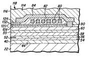
- FIG. 3is a side cross-sectional view depicting various components of a magnetic head 118 of the present invention that may be used as the magnetic head 26 in the disk drive of FIG. 1 .
- the significant features of the present inventionrelate to the structure of the write gap that is fabricated between the magnetic poles. Therefore, the magnetic head of the present invention includes many similar features and structures to those of the prior art magnetic head described hereabove, and such similar features and structures are numbered identically for ease of comprehension.
- the magnetic head 118 of the present inventionincludes a first magnetic shield layer (S 1 ) 40 that is formed upon a surface 44 of the slider body material 22 .
- a read head sensor element 52is disposed within electrical insulation layers 54 and 56 and a second magnetic shield layer (S 2 ) 58 is formed upon the insulation layer 56 .
- An electrical insulation layer 59is then deposited upon the S 2 shield 58 , and a first magnetic pole (P1) 60 is fabricated upon the insulation layer 59 .
- an electrically conductive write gap layer 120 of the present inventionis fabricated upon the P1 pole 60 in steps that are described in detail herebelow with the aid of FIG. 4 .
- a P2 magnetic pole tip 124which includes a photolithographic process including the deposition of a patterned photoresist layer (not shown) including a P2 pole tip trench.
- the photoresistis removed and an induction coil structure including coil turns 80 is then fabricated within insulation 82 above the write gap layer 120 .
- a yoke portion 84 of the second magnetic poleis fabricated in magnetic connection with the P2 pole tip 124 , and through back gap element 90 to the P1 pole 60 .
- Electrical leads(not shown) are subsequently fabricated and a further insulation layer 114 is deposited to encapsulate the magnetic head.
- the magnetic head 118is subsequently fabricated such that an air bearing surface (ABS) 116 is created.
- ABSair bearing surface
- a first preferred embodiment of the write gap layer 120 of the present inventionincludes a first sublayer 128 that is deposited across the surface of the wafer following the fabrication of the P1 pole 60 .
- the sublayer 128is deposited to act as an adhesion layer between the metallic P1 pole layer surface 130 and the subsequent sublayers of the write gap layer 120 of the present invention.
- the adhesion sublayer 128is preferably comprised of a metallic, non-magnetic material such as preferably Ta or Ti, or other acceptable materials such as Cr or NiCr or a combination thereof.
- the adhesion sublayer 128is fabricated with a thickness of from approximately 25 ⁇ to approximately 200 ⁇ , with a preferred thickness of approximately 50 ⁇ .
- a second sublayer 132 of the write gap layer 120is deposited.
- the second sublayer 132is preferably comprised of a non-magnetic, electrically conductive metal, such as preferably Rh or Ru, or other acceptable materials such as Ir, Mo, W, Au, Be, Pd, Pt, Cu, PtMn, and Ta or a combination thereof.
- the sublayer 132is formed with a thickness of from approximately 100 ⁇ to approximately 1000 ⁇ , with a preferred thickness of approximately 500 ⁇ .
- the P2 pole tip 124is directly fabricated thereon, without the necessity for depositing a pole tip seed layer as is done in the prior art (such as seed layer 78 of FIG. 2 ). That is, the non-magnetic electrically conductive write gap sublayer 132 is utilized to conduct electroplating current for the electroplating of the P2 pole tip 124 .
- a photolithographic process similar to the prior art P2 pole tip fabrication processis conducted, wherein a patterned photoresist (not shown) is fabricated upon the sublayer 132 , followed by the electroplating of the P2 pole tip 124 within a P2 pole tip trench formed within the photoresist.
- the electroplating electrical currentflows through the sublayer 132 during the electroplating process.
- the photoresistis removed, such as with the use of a wet chemical stripper, and sublayers 132 and 120 are preferably removed using an ion etching process from all areas except protected areas beneath the P2 pole tip 124 .
- the induction coil structureincluding coil turns 80, yoke portion 84 of the second magnetic pole and further structures as are known in the prior art are fabricated to complete the fabrication of the magnetic head of the present invention.
- the adhesion sublayer 128serves to effectively join the metallic material of the magnetic P1 pole 60 with the metallic electrically conductive sublayer 132 of the write gap layer 120 . Owing primarily to material stress within the P1 magnetic pole material, typically NiFe, delamination of a completed magnetic head at the write gap may occur where an adhesion sublayer is not utilized between the metallic material of the P1 pole 60 and the metallic material forming the write gap sublayer 132 .
- the material that forms the sublayer 132does not readily form an oxide, such that corrosion and tribological problems at the ABS are avoided, and that the sublayer 132 can conduct current to the P2 pole tip in the electroplating process and be plated upon more easily.
- the fabrication of the write gap layer 120allows both a reduction in the thickness of the write gap layer and a reduction in the overall thickness of the P2 magnetic pole tip 124 . That is, a good electrical conductor, such as Rh, allows for the use of a thin sublayer 132 while still supplying adequate electroplating current to plate up the P2 pole tip. Also, because the sublayer 132 is non-magnetic, the overall thickness of the magnetic P2 pole tip is reduced as compared to the prior art P2 pole tip, in which the magnetic seed layer ( 78 in FIG. 2 ) effectively becomes a part of the P2 pole tip due to magnetic flux flow therethrough.
- a good electrical conductorsuch as Rh
- the P2 pole tipis formed with magnetic material such as a CoFe alloy having significantly improved magnetic flux flow properties that are superior to the flux flow properties of the prior art NiFe magnetic seed layer.
- the improved magnetic propertiesare desirable to provide increased magnetic flux flow at greater magnetic flux densities in order to write smaller data bits to the magnetic media.
- the write gap layer 120 of the present invention, with its adhesion sublayer 128are important in this instance where the properties of the electroplated pole may include a large amount of stress which can cause delamination.
- FIG. 5is an enlarged side cross-sectional view depicting an alternative embodiment of a write gap layer 140 of a magnetic head 144 of the present invention.
- the write gap layer 140basically includes three sublayers 148 , 152 and 156 .
- the first sublayer 148is an adhesion sublayer and it is substantially identical to the adhesion sublayer 128 of the magnetic head 118 depicted in FIG. 4 and described hereabove.
- the adhesion sublayer 128is preferably comprised of a metallic, non-magnetic material such as preferably Ta or Ti, or other acceptable materials such as Cr or NiCr or a combination thereof.
- the adhesion sublayer 128is fabricated with a thickness of from approximately 25 ⁇ to approximately 200 ⁇ , with a preferred thickness of approximately 50 ⁇ .
- the middle layer 152is comprised of a non-magnetic material, such as Ta, Ti, W, Mo and Si, which also etchable in a reactive ion etch (RIE) process, such as with the use of oxygen or fluorine active species, as is known to those skilled in the art.
- RIEreactive ion etch
- the thickness of the middle sublayer 152may be from approximately 100 to approximately 1,000 ⁇ , with a preferred thickness of approximately 600 ⁇ .
- the third sublayer 156 of the write gap layer 140is substantially similar to the second sublayer 132 of the write gap layer 120 of the magnetic head 118 depicted in FIG. 4 and described hereabove.
- the third sublayer 156is composed of a non-magnetic, electrically conductive material such as Rh or Ru, or other acceptable materials such as Ir, Mo, W, Au, Be, Pd, Pt, Cu, PtMn, and Ta or a combination thereof, having a thickness of from approximately 100 ⁇ to approximately 1,000 ⁇ with a preferred thickness of approximately 200 ⁇ .
- the third sublayer 156acts as an electrical conductor for the electroplating of the P2 pole tip 124 as has been described hereabove, and where the middle sublayer 152 is also electrically conductive it aids in the conduction of electrical current.
- a P1 pole notching stepis often conducted during the fabrication of a longitudinal magnetic head to substantially eliminate side writing from the P2 pole tip. Specifically, following the fabrication of the P2 pole tip, an ion beam etching step is conducted where the P2 pole tip acts as a etching mask, and the write gap layer and portions of the P1 pole immediately along side of the P2 pole tip are etched away. As a result of the notching step, undesirable side writing of the magnetic head that is caused by the unwanted flow of magnetic flux from the sides of the P2 pole tip to the P1 pole is substantially reduced.
- the significance of the middle sublayer 152 of the write gap structure 140 of the magnetic head 144 of the present inventionis that because it is etchable in an RIE process, the P1 pole notching step is more easily conducted than it is in the prior art P1 pole notching process, where a standard ion beam etching process is utilized. That is, the ion beam P1 pole notching step of the present invention can proceed with greater efficiency by the addition of a reactive component to the ion milling process, because the RIE etchable material of sublayer 152 becomes a gaseous compound in the RIE process, and redeposition of etched material is minimized.
- a write gap layer 140 having three sublayers 148 , 152 and 156provides some improved processing characteristics over the write gap layer 120 having two sublayers 128 and 132 .
- each of the write gap layers 120 and 140include the non-magnetic, electrically conductive sublayer 132 , 156 respectively which acts to carry electrical current in the electroplating of the P2 pole tip thereon.
- the magnetic head 118 and 144 of the present inventioncan be fabricated with a thinner write gap layer and a smaller P2 pole tip. This ultimately facilitates the creation of smaller data bits being written to the magnetic media of a hard disk drive of the present invention, thus increasing the areal data storage density of the hard disk of the hard disk drive and the present invention.
Landscapes
- Engineering & Computer Science (AREA)
- Manufacturing & Machinery (AREA)
- Magnetic Heads (AREA)
Abstract
Description
Claims (28)
Priority Applications (2)
| Application Number | Priority Date | Filing Date | Title |
|---|---|---|---|
| US10/813,880US7265942B2 (en) | 2004-03-30 | 2004-03-30 | Inductive magnetic head with non-magnetic seed layer gap structure and method for the fabrication thereof |
| CNB2004101003554ACN100346393C (en) | 2004-03-30 | 2004-12-09 | Inductive magnetic head with non-magnetic seed layer gap structure and method for the fabrication thereof |
Applications Claiming Priority (1)
| Application Number | Priority Date | Filing Date | Title |
|---|---|---|---|
| US10/813,880US7265942B2 (en) | 2004-03-30 | 2004-03-30 | Inductive magnetic head with non-magnetic seed layer gap structure and method for the fabrication thereof |
Publications (2)
| Publication Number | Publication Date |
|---|---|
| US20050219745A1 US20050219745A1 (en) | 2005-10-06 |
| US7265942B2true US7265942B2 (en) | 2007-09-04 |
Family
ID=35049973
Family Applications (1)
| Application Number | Title | Priority Date | Filing Date |
|---|---|---|---|
| US10/813,880Expired - Fee RelatedUS7265942B2 (en) | 2004-03-30 | 2004-03-30 | Inductive magnetic head with non-magnetic seed layer gap structure and method for the fabrication thereof |
Country Status (2)
| Country | Link |
|---|---|
| US (1) | US7265942B2 (en) |
| CN (1) | CN100346393C (en) |
Cited By (5)
| Publication number | Priority date | Publication date | Assignee | Title |
|---|---|---|---|---|
| US8196285B1 (en) | 2008-12-17 | 2012-06-12 | Western Digital (Fremont), Llc | Method and system for providing a pole for a perpendicular magnetic recording head using a multi-layer hard mask |
| US8225488B1 (en) | 2009-05-22 | 2012-07-24 | Western Digital (Fremont), Llc | Method for providing a perpendicular magnetic recording (PMR) pole |
| US8254060B1 (en) | 2009-04-17 | 2012-08-28 | Western Digital (Fremont), Llc | Straight top main pole for PMR bevel writer |
| US9346672B1 (en) | 2009-08-04 | 2016-05-24 | Western Digital (Fremont), Llc | Methods for fabricating damascene write poles using ruthenium hard masks |
| US11823712B2 (en) | 2020-08-19 | 2023-11-21 | Headway Technologies, Inc. | Built-in resistance sensor for measuring slider level pole width at point “A” (PWA) for PMR/MAMR writers |
Families Citing this family (8)
| Publication number | Priority date | Publication date | Assignee | Title |
|---|---|---|---|---|
| US7525760B2 (en)* | 2005-04-11 | 2009-04-28 | Hitachi Global Storage Technologies B.V. | Laminated write gap to improve writer performance |
| US7500302B2 (en)* | 2005-04-11 | 2009-03-10 | Hitachi Global Storage Technologies, Netherlands B.V. | Process for fabricating a magnetic recording head with a laminated write gap |
| US8259411B2 (en)* | 2008-05-07 | 2012-09-04 | Seagate Technology Llc | Fabrication of trapezoidal pole for magnetic recording |
| CN102156722B (en)* | 2011-03-30 | 2014-04-09 | 中国工商银行股份有限公司 | System and method for processing mass data |
| CN102982812A (en)* | 2012-12-04 | 2013-03-20 | 新乡医学院 | Method for producing magnetic head wafer of hard disk |
| US10903319B2 (en)* | 2016-06-15 | 2021-01-26 | Nanomedical Diagnostics, Inc. | Patterning graphene with a hard mask coating |
| JP7166204B2 (en)* | 2019-03-11 | 2022-11-07 | 株式会社東芝 | Magnetic head and magnetic recording device |
| JP7319603B2 (en)* | 2019-09-06 | 2023-08-02 | 株式会社東芝 | Magnetic head and magnetic recording device |
Citations (18)
| Publication number | Priority date | Publication date | Assignee | Title |
|---|---|---|---|---|
| US3718776A (en)* | 1970-12-11 | 1973-02-27 | Ibm | Multi-track overlapped-gap magnetic head, assembly |
| JPS61110319A (en) | 1984-10-31 | 1986-05-28 | Nec Kansai Ltd | Production of thin-film magnetic head |
| JPS62145523A (en) | 1985-12-20 | 1987-06-29 | Hitachi Ltd | thin film magnetic head |
| US5285340A (en) | 1992-02-28 | 1994-02-08 | International Business Machines Corporation | Thin film magnetic head with conformable pole tips |
| US5673163A (en) | 1992-10-20 | 1997-09-30 | Cohen; Uri | Pinched-gap magnetic recording thin film head |
| JPH11213332A (en) | 1998-01-22 | 1999-08-06 | Hitachi Ltd | Thin-film magnetic head and magnetic disk drive |
| US6151193A (en) | 1997-05-27 | 2000-11-21 | Tdk Corporation | Thin film magnetic head |
| US6173486B1 (en) | 1997-03-04 | 2001-01-16 | Read-Rite Corporation | Thin film magnetic head with self-aligned pole tips |
| US6239948B1 (en) | 1999-07-23 | 2001-05-29 | Headway Technologies, Inc. | Non-magnetic nickel containing conductor alloys for magnetic transducer element fabrication |
| JP2002140803A (en) | 2000-11-02 | 2002-05-17 | Hitachi Ltd | Magnetic head, method of manufacturing magnetic head, and magnetic disk drive using the same |
| JP2002298310A (en) | 2001-04-02 | 2002-10-11 | Alps Electric Co Ltd | Thin film magnetic head and method of manufacturing it |
| US20020167759A1 (en) | 2001-05-08 | 2002-11-14 | Alps Electric Co., Ltd. | Magnetic write head having enhanced saturation magnetic flux around gap layer |
| US20030030940A1 (en) | 2001-06-20 | 2003-02-13 | Naoto Matono | Thin film magnetic head and method of manufacturing same |
| US20030072970A1 (en) | 2001-10-05 | 2003-04-17 | Headway Technologies, Inc. | Layered structure for magnetic recording heads |
| US6600629B2 (en) | 2000-12-07 | 2003-07-29 | Alps Electric Co., Ltd. | Thin film magnetic head having gap layer made of nip and method of manufacturing the same |
| US6724569B1 (en)* | 2000-02-16 | 2004-04-20 | Western Digital (Fremont), Inc. | Thin film writer with multiplayer write gap |
| US6833976B2 (en)* | 2002-05-15 | 2004-12-21 | International Business Machine Corporation | Thin film magnetic recording inductive write head with laminated write gap |
| US6960281B2 (en)* | 2003-03-21 | 2005-11-01 | Headway Technologies, Inc. | Method to make a wider trailing pole structure by self-aligned pole trim process |
Family Cites Families (1)
| Publication number | Priority date | Publication date | Assignee | Title |
|---|---|---|---|---|
| JP3464379B2 (en)* | 1998-03-27 | 2003-11-10 | Tdk株式会社 | Thin film magnetic head and method of manufacturing the same |
- 2004
- 2004-03-30USUS10/813,880patent/US7265942B2/ennot_activeExpired - Fee Related
- 2004-12-09CNCNB2004101003554Apatent/CN100346393C/ennot_activeExpired - Fee Related
Patent Citations (19)
| Publication number | Priority date | Publication date | Assignee | Title |
|---|---|---|---|---|
| US3718776A (en)* | 1970-12-11 | 1973-02-27 | Ibm | Multi-track overlapped-gap magnetic head, assembly |
| JPS61110319A (en) | 1984-10-31 | 1986-05-28 | Nec Kansai Ltd | Production of thin-film magnetic head |
| JPS62145523A (en) | 1985-12-20 | 1987-06-29 | Hitachi Ltd | thin film magnetic head |
| US5285340A (en) | 1992-02-28 | 1994-02-08 | International Business Machines Corporation | Thin film magnetic head with conformable pole tips |
| US5673163A (en) | 1992-10-20 | 1997-09-30 | Cohen; Uri | Pinched-gap magnetic recording thin film head |
| US6173486B1 (en) | 1997-03-04 | 2001-01-16 | Read-Rite Corporation | Thin film magnetic head with self-aligned pole tips |
| US6151193A (en) | 1997-05-27 | 2000-11-21 | Tdk Corporation | Thin film magnetic head |
| JPH11213332A (en) | 1998-01-22 | 1999-08-06 | Hitachi Ltd | Thin-film magnetic head and magnetic disk drive |
| US6239948B1 (en) | 1999-07-23 | 2001-05-29 | Headway Technologies, Inc. | Non-magnetic nickel containing conductor alloys for magnetic transducer element fabrication |
| US6724569B1 (en)* | 2000-02-16 | 2004-04-20 | Western Digital (Fremont), Inc. | Thin film writer with multiplayer write gap |
| JP2002140803A (en) | 2000-11-02 | 2002-05-17 | Hitachi Ltd | Magnetic head, method of manufacturing magnetic head, and magnetic disk drive using the same |
| US6600629B2 (en) | 2000-12-07 | 2003-07-29 | Alps Electric Co., Ltd. | Thin film magnetic head having gap layer made of nip and method of manufacturing the same |
| JP2002298310A (en) | 2001-04-02 | 2002-10-11 | Alps Electric Co Ltd | Thin film magnetic head and method of manufacturing it |
| US20020167759A1 (en) | 2001-05-08 | 2002-11-14 | Alps Electric Co., Ltd. | Magnetic write head having enhanced saturation magnetic flux around gap layer |
| US20030030940A1 (en) | 2001-06-20 | 2003-02-13 | Naoto Matono | Thin film magnetic head and method of manufacturing same |
| US20030072970A1 (en) | 2001-10-05 | 2003-04-17 | Headway Technologies, Inc. | Layered structure for magnetic recording heads |
| US6833976B2 (en)* | 2002-05-15 | 2004-12-21 | International Business Machine Corporation | Thin film magnetic recording inductive write head with laminated write gap |
| US6975485B2 (en)* | 2002-05-15 | 2005-12-13 | International Business Machines Corporation | Thin film magnetic recording inductive write head with laminated write gap |
| US6960281B2 (en)* | 2003-03-21 | 2005-11-01 | Headway Technologies, Inc. | Method to make a wider trailing pole structure by self-aligned pole trim process |
Cited By (6)
| Publication number | Priority date | Publication date | Assignee | Title |
|---|---|---|---|---|
| US8196285B1 (en) | 2008-12-17 | 2012-06-12 | Western Digital (Fremont), Llc | Method and system for providing a pole for a perpendicular magnetic recording head using a multi-layer hard mask |
| US8254060B1 (en) | 2009-04-17 | 2012-08-28 | Western Digital (Fremont), Llc | Straight top main pole for PMR bevel writer |
| US8893376B1 (en) | 2009-04-17 | 2014-11-25 | Western Digital(Fremont), LLC | Method of forming a straight top main pole for PMR bevel writer |
| US8225488B1 (en) | 2009-05-22 | 2012-07-24 | Western Digital (Fremont), Llc | Method for providing a perpendicular magnetic recording (PMR) pole |
| US9346672B1 (en) | 2009-08-04 | 2016-05-24 | Western Digital (Fremont), Llc | Methods for fabricating damascene write poles using ruthenium hard masks |
| US11823712B2 (en) | 2020-08-19 | 2023-11-21 | Headway Technologies, Inc. | Built-in resistance sensor for measuring slider level pole width at point “A” (PWA) for PMR/MAMR writers |
Also Published As
| Publication number | Publication date |
|---|---|
| CN100346393C (en) | 2007-10-31 |
| US20050219745A1 (en) | 2005-10-06 |
| CN1677496A (en) | 2005-10-05 |
Similar Documents
| Publication | Publication Date | Title |
|---|---|---|
| US6912106B1 (en) | Writer with a hot seed zero throat and substantially flat top pole | |
| US7120988B2 (en) | Method for forming a write head having air bearing surface (ABS) | |
| US8056213B2 (en) | Method to make PMR head with integrated side shield (ISS) | |
| US8230583B2 (en) | Method for manufacturing a magnetic write head | |
| US6975486B2 (en) | Thin film write head having a laminated, flat top pole with bottom shaper and method of fabrication | |
| US8424192B1 (en) | Method for manufacturing a pole for a magnetic recording head | |
| JP4633155B2 (en) | Manufacturing method of thin film magnetic head | |
| US8844120B1 (en) | Method for providing a magnetic recording transducer including an assist pole having surfaces angled with respect to the ABS | |
| US8470186B2 (en) | Perpendicular write head with wrap around shield and conformal side gap | |
| US8861134B1 (en) | Method and system for providing perpendicular magnetic recording transducers utilizing a damascene approach | |
| US7536777B2 (en) | Use of metal capped seed layers for the fabrication of perpendicular thin film heads | |
| US7995307B2 (en) | Perpendicular magnetic recording write head with trailing shield having throat height defined by electroplated nonmagnetic pad layer and method for making the head | |
| US8201320B2 (en) | Method for manufacturing a magnetic write head having a wrap around shield that is magnetically coupled with a leading magnetic shield | |
| JPH11120513A (en) | Thin-film magnetic head and its production | |
| US7265942B2 (en) | Inductive magnetic head with non-magnetic seed layer gap structure and method for the fabrication thereof | |
| US7119988B2 (en) | Perpendicular magnetic head having modified shaping layer for direct plating of magnetic pole piece | |
| US7228619B2 (en) | Method of manufacturing a magnetic head with common seed layer for coil and pedestal | |
| US7101633B2 (en) | Electroplated magnetic thin film, method of manufacturing the same, electroplating bath and thin film magnetic head | |
| US8177955B2 (en) | Electrodeposition of FeCoNiV films with high resistivity and high saturation magnetization for magnetic head fabrication | |
| US6345435B1 (en) | Method to make laminated yoke for high data rate giant magneto-resistive head | |
| JP2000231705A (en) | Thin film magnetic head and method of manufacturing the same | |
| JP2009151911A (en) | Magnetic head manufacturing method, magnetic head, and magnetic recording apparatus |
Legal Events
| Date | Code | Title | Description |
|---|---|---|---|
| AS | Assignment | Owner name:HITACHI GLOBAL STORAGE TECHNOLOGIES NETHERLANDS BV Free format text:ASSIGNMENT OF ASSIGNORS INTEREST;ASSIGNORS:HIXSON-GOLDSMITH, APRIL DAWN;LILLE, JEFFREY S.;REEL/FRAME:015174/0597;SIGNING DATES FROM 20040323 TO 20040326 | |
| FEPP | Fee payment procedure | Free format text:PAYOR NUMBER ASSIGNED (ORIGINAL EVENT CODE: ASPN); ENTITY STATUS OF PATENT OWNER: LARGE ENTITY | |
| STCF | Information on status: patent grant | Free format text:PATENTED CASE | |
| FPAY | Fee payment | Year of fee payment:4 | |
| AS | Assignment | Owner name:HGST, NETHERLANDS B.V., NETHERLANDS Free format text:CHANGE OF NAME;ASSIGNOR:HGST, NETHERLANDS B.V.;REEL/FRAME:029341/0777 Effective date:20120723 Owner name:HGST NETHERLANDS B.V., NETHERLANDS Free format text:CHANGE OF NAME;ASSIGNOR:HITACHI GLOBAL STORAGE TECHNOLOGIES NETHERLANDS B.V.;REEL/FRAME:029341/0777 Effective date:20120723 | |
| FPAY | Fee payment | Year of fee payment:8 | |
| AS | Assignment | Owner name:WESTERN DIGITAL TECHNOLOGIES, INC., CALIFORNIA Free format text:ASSIGNMENT OF ASSIGNORS INTEREST;ASSIGNOR:HGST NETHERLANDS B.V.;REEL/FRAME:040819/0450 Effective date:20160831 | |
| FEPP | Fee payment procedure | Free format text:MAINTENANCE FEE REMINDER MAILED (ORIGINAL EVENT CODE: REM.); ENTITY STATUS OF PATENT OWNER: LARGE ENTITY | |
| LAPS | Lapse for failure to pay maintenance fees | Free format text:PATENT EXPIRED FOR FAILURE TO PAY MAINTENANCE FEES (ORIGINAL EVENT CODE: EXP.); ENTITY STATUS OF PATENT OWNER: LARGE ENTITY | |
| STCH | Information on status: patent discontinuation | Free format text:PATENT EXPIRED DUE TO NONPAYMENT OF MAINTENANCE FEES UNDER 37 CFR 1.362 | |
| FP | Lapsed due to failure to pay maintenance fee | Effective date:20190904 |