US7265633B1 - Open loop bandwidth test architecture and method for phase locked loop (PLL) - Google Patents
Open loop bandwidth test architecture and method for phase locked loop (PLL)Download PDFInfo
- Publication number
- US7265633B1 US7265633B1US11/132,894US13289405AUS7265633B1US 7265633 B1US7265633 B1US 7265633B1US 13289405 AUS13289405 AUS 13289405AUS 7265633 B1US7265633 B1US 7265633B1
- Authority
- US
- United States
- Prior art keywords
- test
- pll
- circuit
- coupled
- current
- Prior art date
- Legal status (The legal status is an assumption and is not a legal conclusion. Google has not performed a legal analysis and makes no representation as to the accuracy of the status listed.)
- Expired - Lifetime, expires
Links
Images


Classifications
- H—ELECTRICITY
- H03—ELECTRONIC CIRCUITRY
- H03L—AUTOMATIC CONTROL, STARTING, SYNCHRONISATION OR STABILISATION OF GENERATORS OF ELECTRONIC OSCILLATIONS OR PULSES
- H03L7/00—Automatic control of frequency or phase; Synchronisation
- H03L7/06—Automatic control of frequency or phase; Synchronisation using a reference signal applied to a frequency- or phase-locked loop
- H03L7/08—Details of the phase-locked loop
- H03L7/085—Details of the phase-locked loop concerning mainly the frequency- or phase-detection arrangement including the filtering or amplification of its output signal
- H03L7/089—Details of the phase-locked loop concerning mainly the frequency- or phase-detection arrangement including the filtering or amplification of its output signal the phase or frequency detector generating up-down pulses
- H03L7/0891—Details of the phase-locked loop concerning mainly the frequency- or phase-detection arrangement including the filtering or amplification of its output signal the phase or frequency detector generating up-down pulses the up-down pulses controlling source and sink current generators, e.g. a charge pump
- H—ELECTRICITY
- H03—ELECTRONIC CIRCUITRY
- H03L—AUTOMATIC CONTROL, STARTING, SYNCHRONISATION OR STABILISATION OF GENERATORS OF ELECTRONIC OSCILLATIONS OR PULSES
- H03L7/00—Automatic control of frequency or phase; Synchronisation
- H03L7/06—Automatic control of frequency or phase; Synchronisation using a reference signal applied to a frequency- or phase-locked loop
- H03L7/08—Details of the phase-locked loop
- H03L7/085—Details of the phase-locked loop concerning mainly the frequency- or phase-detection arrangement including the filtering or amplification of its output signal
- H03L7/093—Details of the phase-locked loop concerning mainly the frequency- or phase-detection arrangement including the filtering or amplification of its output signal using special filtering or amplification characteristics in the loop
Definitions
- the present inventionrelates generally to electronic circuits, and more particularly to circuits that generate timing signals.
- timing signalscan be very important to the overall performance of the system.
- One widely used way to synchronize operations of a system (e.g., integrated circuit) with an externally received clockcan be with a phase locked loop (PLL).
- PLLscan address many common timing problems associated with generating a clock signal, including but not limited to, unwanted clock skew and jitter.
- PLLsare widely in used in applications other than frequency synchronization, including but not limited to frequency synthesis, frequency translation, frequency detection, and frequency modulation.
- FIG. 9shows a block schematic diagram of a conventional third order PLL designated by the general reference character 900 .
- FIG. 9shows a basic “charge pump” style PLL, in which a charge pump generates a control (or error) voltage on a capacitance by “pumping” the potential up or down.
- Such a basic charge pump style PLLis commonly used for frequency synthesis applications.
- a PLL 900can include a phase frequency detector 902 , charge pump 904 , a loop filter (with passive components resistor R L , capacitor C L , and capacitor C S ) 906 , a voltage controlled oscillator (VCO) 908 , and a feedback divider 910 .
- These blocks of a PLL 900can form a negative feedback loop that operates to match the phases and frequencies of the two PFD input signals, ⁇ IN and ⁇ FBK .
- a feedback divider 910can allow the synthesized output signal to operate at “P” times the input frequency, thus enabling the PLL to generate an output signal ⁇ OUT in phase but greater in frequency than the reference input signal ⁇ IN .
- a loop frequency responsecan be important for determining the stability of the overall circuit.
- the total loop phase shiftmust typically be less than 180 degrees when the open loop gain falls below 0 dB (at the open loop bandwidth).
- the stable loop frequency range in the PLLcan be far less variable over process and environmental conditions (due mostly to RC component variations of the loop filter) than the open loop bandwidth. Therefore, knowledge of the open loop bandwidth within the less variable stable loop frequency range can show the relative stability of the PLL. For example, if the open loop bandwidth is beyond the stable loop frequency range window, one can reasonably infer either instability or well under-damped stability.
- the PLL open loop bandwidthcan be found as shown in Eq. 2.1.
- OLG ⁇ ( s )⁇ I CP ⁇ s ⁇ ⁇ ⁇ L + 1 s ⁇ ( C L + C S ) ⁇ ( s ⁇ ⁇ ⁇ S + 1 ) ⁇ K VCO s ⁇ 1 P Eq .
- ⁇ L⁇ R L ⁇ C L
- ⁇ SC L ⁇ C S C L + C S ⁇ R L
- OLBW⁇ K VCO ⁇ I CP ⁇ R L ⁇ C L P ⁇ ( C L + C S )
- PLL test measurements taken during productiontypically include only a “lock” test, which can reveal PLL stability in a binary sense (true/false), but reveals no other information about the PLL loop dynamics.
- the present inventioncan include a phase locked loop (PLL) circuit that includes a test loop filter.
- a test loop filtercan include a resistor-capacitor (RC) network coupled to a control node.
- a controlcan be coupled to a voltage controlled oscillator (VCO).
- the test loop filtercan also incorporate a test leg coupled to the RC network that includes a test resistance, and at least one test controllable impedance path in series with the test resistance. The test leg can provide a high impedance in a non-test mode and a low impedance in a test mode.
- a currentcan be caused to flow through a loop filter resistance to thereby generate a voltage at the control node that can be controlled in order to test PLL circuit parameters.
- a test controllable impedance pathcan comprise a transistor.
- test capabilitiescan be added to an existing PLL circuit design with the addition of only a few circuit components.
- an RC networkcan include a load resistance and a first filter capacitor in series with one another between the control node and a first power supply node.
- a test legcan be coupled in series with the load resistance and in parallel with the first filter capacitor. More particularly, a load resistance can be coupled to the first filter capacitor at a filter node, and the test leg can include a test resistance coupled to the first filter node and the test controllable impedance path coupled between test resistance and the first power supply node.
- a test legcan further include an offset voltage circuit coupled in series with a test resistance.
- a test resistancecan be a variable resistance that is varied in the test mode. In this way, different control voltages can be generated based on resistance values, as opposed to a varying test current value.
- a PLL circuitcan further include an adjustable current supply that provides a selectable current to the control node in the test mode.
- an adjustable current supplycan be an existing section of a charge pump circuit that provides a current supply based on a phase difference signal in the non-test mode.
- a PLL circuitcan further include a phase detector circuit that provides a phase difference value.
- the phase difference valuecan vary according to test input values.
- the phase difference valuecan be based a difference between an input signal and feedback signal.
- a charge pump circuitcan be coupled to the control node and provide a current to the control node based on the phase difference value output from the phase detector circuit. In this way, different control voltages can be generated based on a test values provided to a phase detector circuit.
- a PLL circuitcan further include a phase detector that generates a phase different value based on a phase difference between an input signal and a feedback signal.
- a charge pumpcan be coupled between the phase detector and control node that provides a current to the control node based on the phase difference value.
- a feedback pathcan be coupled between an output of the VCO and an input of the phase detector.
- the feedback pathcan include a loop switch that opens the feedback path in the test mode and remains closed in a non-test mode. In this way, different control voltages can be generated based on opening a feedback path of the PLL circuit.
- the loop filteris formed in the same integrated circuit substrate as other portions of the PLL.
- a PLL manufactured as an integrated or as a portion of an integrated circuitcan be easily tested for an open loop bandwidth value.
- the present inventioncan also include a method of testing a PLL circuit.
- the methodcan include enabling a test leg that draws current through a load resistance of a PLL loop filter to generate a control voltage at an input of a voltage controlled oscillator.
- the methodcan also include varying the control voltage and measuring the output frequency of the PLL for each of the different control voltages. Such a method can help arrive at an open loop bandwidth determination for a PLL without invasive or time consuming testing.
- a PLL circuitcan be formed in an integrated circuit. Further, enabling the test leg comprises turning on a transistor in response to a test signal applied from a source external to the integrated circuit.
- varying a control voltagecan include providing a first test current of magnitude “I” to generate one control voltage, and providing currents having a multiple of “I” to generate a plurality of other control voltages.
- varying a control voltagecan include outputting predetermined different phase difference values from a phase detector and generating test currents in response to each different phase difference value. Such test currents can be provided to the loop filter.
- varying a control voltagecan include opening a feedback loop of the PLL.
- a methodcan further include performing a linear regression on output frequency measurements and corresponding values used to vary the control voltage.
- the present inventioncan also include a PLL having a test loop filter that includes a load resistor coupled to a control voltage node and a test leg that provides a current path through the load resistor that is disabled in a non-test mode and enabled in a test mode.
- the PLLcan also include a voltage controlled oscillator coupled to the test loop filter that generates an output signal having a frequency determined, at least in part, on a voltage generated on the control voltage node.
- a test loop filtercan include a load resistor coupled in series with a first load capacitor, and a switch element coupled between the load resistor and a power supply node.
- a PLLcan further include a variable supply current circuit that provides an output current to the test loop filter that has a magnitude that can be varied in response to test signals in the test mode.
- FIG. 1is a block schematic diagram of a first embodiment of the present invention.
- FIG. 2is a block schematic diagram of a second embodiment of the present invention.
- FIG. 3is a block schematic diagram of a third embodiment of the present invention.
- FIG. 4is a block schematic diagram of a fourth embodiment of the present invention.
- FIG. 5is a block schematic diagram of a fifth embodiment of the present invention.
- FIG. 6is a block schematic diagram of a sixth embodiment of the present invention.
- FIG. 7Ais a block schematic diagram of a testing arrangement according to an embodiment of the present invention.
- FIG. 7Bis a block diagram of one example of a device under test like that shown in FIG. 7A .
- FIG. 8is a table showing a test method according to an embodiment of the present invention.
- FIG. 9is a block schematic diagram of a conventional phase locked loop circuit.
- the embodimentsinclude a loop filter circuit, phase locked loop (PLL) circuit, and test method that can arrive at an open loop gain measurement for a PLL circuit that may be less invasive, faster, and simpler than conventional approaches.
- PLLphase locked loop
- a first embodiment of the present inventioncan include a test loop filter of a PLL circuit.
- a test loop filteris designated by the general reference character 100 , and can include a resistor-capacitor (RC) network 102 and a test leg 104 .
- An RC network 102can be situated between a control node 106 and a supply node 108 (in this case a low voltage power supply node, such as ground).
- RC network 102can include a load resistance RL, a first capacitor CL, and a second capacitor CS.
- a load resistance RLcan be connected in series with first capacitor CL between a control node 106 and supply node 108 .
- a second capacitor CScan be connected in parallel with load resistor RL and first capacitor CL between control node 106 and supply node 108 .
- a test leg 104can be connected to a load resistance RL, and when enabled, can provide a current path through load resistance RL.
- a test leg 104can include a test resistance RS 104 - 0 arranged in series with a switch element 1041 .
- Test resistance RS 104 - 0can be connected at a node that joins load resistance RL with first capacitor CL.
- a switch element 104 - 1can provide an impedance path that is controllable in response to a signal TestOn.
- switch element 104 - 1can provide a low impedance path.
- switch element 104 - 1can provide a high impedance path.
- test leg 104should not be construed as limiting to the invention (i.e., a switch element 104 - 1 can be connected between a load resistance RL and test resistance RS 104 - 0 ).
- switch element 104 - 1can provide a high impedance and RC network 102 can operate in the same essential way as conventional loop filter 906 shown in FIG. 9 , generating a control voltage V CTRL at control node 106 due to the total charge delivered during by a PLL charge pump during acquisition and lock.
- switch element 104 - 1can provide a low impedance. Consequently, loop filter 100 can provide a control voltage V CTRL that corresponds to the current flowing through load resistance RL and test resistance RS. This can enable the acquisition of test data for measuring the open loop gain for a PLL circuit containing the loop filter 100 . More details and examples of such measurements will be described below.
- FIG. 2shows a second embodiment of a loop filter, designated by the general reference character 200 .
- a second embodiment 200can include some of the same circuit components as the first embodiment 100 . Thus, like components are referred to by the same reference character but with the first digit begin a “2” instead of a “1”.
- a second embodiment loop filter 200can differ from the first embodiment in that a test leg 204 ′ may also include an offset voltage circuit 204 - 2 .
- An offset voltage circuit 204 - 2can introduce an offset voltage component V OFFSET to a control voltage V CTRL .
- FIG. 3shows a third embodiment of a loop filter, designated by the general reference character 300 .
- a third embodiment 300can include some of the same circuit components as the second embodiment 200 . Thus, like components are referred to by the same reference character but with the first digit begin a “3” instead of a “2”.
- a third embodiment loop filter 300can differ from the second and first embodiments in that a switch element 304 - 1 ′ can include a insulated gate field effect transistor (e.g., a pull-down MOSFET M 1 ) having a source-drain path coupled between a load resistance RL and a power supply voltage node 308 , and a gate that receives a signal TestOn.
- a switch element 304 - 1 ′can include a insulated gate field effect transistor (e.g., a pull-down MOSFET M 1 ) having a source-drain path coupled between a load resistance RL and a power supply voltage node 308 , and a gate that receives a signal TestOn.
- a switch element 304 - 1 ′can include a insulated gate field effect transistor (e.g., a pull-down MOSFET M 1 ) having a source-drain path coupled between a load resistance RL and a power supply voltage node 308 , and a gate that receive
- a loop filterwith added components of a test leg, can preferably be formed in the same substrate that contains the corresponding PLL circuit.
- test capabilitiescan be introduced into a PLL circuit by adding only a few additional circuit components to an existing PLL circuit design.
- a current provided to a loop filtercan be adjusted, or otherwise selected by a testing device and/user. More particularly, when a switch element (e.g., the pull-down MOSFET M 1 ) is turned “on,” current can flow through a load resistor R L . Voltage can be generated across R L by forcing a charge pump UP current (I UP ) “on.” An UP current, I UP , can be forced “on” using a number of techniques, a few of which are illustrated below in FIGS. 4 to 6 .
- charge pump PLLscan have a built in charge pump current varying capability where the value is changed by X times a reference value I REF (where X can take a number of values greater than one).
- a charge pump valuecan be alterable by external part pin programming (using any common method via a part tester).
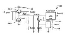
- FIG. 4shows a block schematic diagram of a PLL circuit section according to a fourth embodiment.
- a PLL circuit sectionis designated by the general reference character 400 can include a test loop filter 402 , voltage controlled oscillator (VCO) 404 , and charge pump circuit 406 .
- VCOvoltage controlled oscillator
- a test loop filter 402can take the form of any of the above embodiments or equivalents, and can provide a control voltage V CTRL that depends upon a current provided to loop filter 402 from charge pump circuit 406 .
- a VCO 404can generate an output signal ⁇ OUT having a frequency that depends upon control voltage V CTRL .
- FIG. 4illustrates a case in which a current I UP provided to a test loop filter 402 during a test can be generated by additional current switching in the charge pump 404 . More particularly, a charge pump 404 may provide a current I UP from a controllable current source 406 - 0 to a loop filter 402 according to test value TestCtrl.
- current I UPcan be based on a phase difference value ⁇ phase generated by a phase detector circuit, or the like.
- capacitorsi.e., CS and CL
- loop filter 402can be charged up to create a larger control voltage V CTRL when a phase difference exist (e.g., lag or lead), and thereby increase the frequency of VCO output signal ⁇ OUT .
- a charge pump 404may optionally include another controllable current source (or discharge path) 406 - 1 that discharges capacitors (i.e., CS and CL) within loop filter 402 to decrease control voltage V CTRL when an opposite phase difference exist (e.g., lead or lag), and thereby decrease the frequency of VCO output signal ⁇ OUT .
- another controllable current source (or discharge path) 406 - 1that discharges capacitors (i.e., CS and CL) within loop filter 402 to decrease control voltage V CTRL when an opposite phase difference exist (e.g., lead or lag), and thereby decrease the frequency of VCO output signal ⁇ OUT .
- a current I UPcan be based on a test established value TestCtrl.
- a control voltage V CTRLcan be generated that is based on a voltage generated across load resistance RL and any test resistance (and/or offset voltage) present in a test leg 408 , rather than on charged capacitors.
- a value of current I UPcan be varied to generate multiple data points, each corresponding to a different current value I UP (or control voltage value I UP can).
- the values of current I UPcan include a reference current I REF and a number of multiples of the reference current X*I REF (where 1 ⁇ X ⁇ N, and N is an integer greater than 2).
- charge pump current switchingcan be used to provide different current levels to a test loop filter in a test mode.
- FIG. 5shows a block schematic diagram of a PLL circuit section according to a fifth embodiment.
- a PLL circuit sectionis designated by the general reference character 500 can include some of the same general components as the embodiment of FIG. 4 . Thus, like components are referred to by the same reference character but with the first digit begin a “5” instead of a “4”.
- a PLL circuit section 500can differ from that of FIG. 4 in that a charge pump 506 ′ can be conventional in design, and not provide additional current switching in a test mode. Further, a PLL circuit section 500 can also include an adjustable phase detector (PFD) 508 .
- An adjustable PFD 508can include additional logic over a conventional PFD that enables the adjustable PFD 508 to generate a phase difference value that does not only depend upon a difference between an input signal and feedback signal.
- a phase difference value ⁇ phasecan be generated by a PDF 508 based on a phase difference between an input signal ⁇ IN and a feedback signal ⁇ FBK .
- a charge pump 506 ′can provide a current I UP (and optionally I DWN ) to test loop filter 508 . That is, the PLL circuit section 500 operates in a conventional fashion.
- phase difference value ⁇ phasecan be based on a test established value TestCtrl.
- a control voltage V CTRLcan be generated that is based on a voltage generated across load resistance RL and any test resistance (and/or offset voltage) present in a test leg 508 , rather than on charged capacitors.
- a phase difference valuecan be varied to generate various data points, as noted above in the description of the fourth embodiment.
- phase detector outputcan be used to provide different current levels to a test loop filter in a test mode.
- FIG. 6shows a block schematic diagram of a PLL circuit section according to a sixth embodiment.
- a PLL circuitis designated by the general reference character 600 can include some of the same general components as the embodiment of FIG. 5 . Thus, like components are referred to by the same reference character but with the first digit begin a “6” instead of a “5”.
- a PLL circuit 600can differ from that of FIG. 5 in that a phase detector circuit 608 ′ can be conventional in design, and not provide a test selectable phase difference value ⁇ phase.
- a PLL circuit section 600can include a feedback path 610 that can feed back a signal from VCO 604 to PFD 608 ′.
- a feedback path 610can include a loop switch element 612 and, optionally, a frequency divider 614 .
- FIG. 6illustrates a case in which a test current I UP provided to a test loop filter 602 during a test can be generated by opening feedback path 610 .
- loop switch element 612provides a low impedance, enabling feedback path 610 and thereby providing a feedback signal ⁇ FBK to PFD 608 . This completes a negative feedback loop that forces feedback signal ⁇ FBK to match input signal ⁇ IN .
- a loop switch element 612can provide a high impedance path that disables feedback path 610 . This opens the negative feedback loop of the PLL circuit.
- PDF 608 ′can generate a phase difference value ⁇ phase that causes charge pump 606 ′ to provide a current I UP to test loop filter 602 .
- a control voltage V CTRLcan be generated that is based on a voltage generated across load resistance RL and any test resistance (and/or offset voltage) present in a test leg 508 , rather than on charged capacitors.
- a phase difference valuecan be varied to generate various data points, as noted above in the description of the fourth embodiment. As but one very particular example, multiple phase difference values can be generated by opening a feedback loop for different amounts of time.
- a feedback loopcan be opened to provide different current levels to a test loop filter in a test mode.
- a switch elemente.g., transistor M 1
- V OFFSETan optional voltage offset
- a VCOcan generate an output frequency determined by the following Eq. 4.1.
- F OUTK VCO *V CTRL +F OFFSET Eq. 4.1
- F OUTis the frequency of a signal output from a VCO
- K VCOis the VCO frequency vs. control voltage transfer function
- I UPis a current provided to a test loop filter (e.g., from a charge pump, or the like)
- R Lis a load resistance
- R Sis a test resistance
- V OFFSETis the offset voltage
- F OFFSETis an inherent VCO frequency offset.
- OLBWK VCO ⁇ I CP ⁇ R L ⁇ C L P ⁇ ( C L + C S ) Eq . ⁇ 4.4
- the remaining loop filter capacitor and resistor ratio and feedback divider termscan be fixed quantities that are determined in the design and do not change significantly with process variation. Therefore, this measurement can arrive at a PLL open loop bandwidth measurement, which as note above, can indicate PLL stability and can be used to estimate its closed loop bandwidth.
- a testing system 700can include a device under test (DUT) 702 , which can be an integrated circuit in which is formed a PLL circuit 704 .
- DUTdevice under test
- a PLL circuit 704that may include any of the above embodiments, or equivalents.
- a tester 706can apply test signals to a DUT 702 in a conventional fashion, such as at package pins, bond pads or test pads.
- a tester 706can provide power (e.g., VCC and ground) to bond pads via power outputs 708 , test control signals via one or more test control outputs 710 , and receive an output signal via a test input 712 .
- powere.g., VCC and ground
- a tester 706can include memory 706 - 0 for storing a test program for execution by a processor 706 - 1 .
- a tester 706can include a frequency measuring circuit 706 - 2 .
- a tester 706can be connected to a DUT 702 by conventional tester connections, including but not limited to socket connections that hold a DUT 702 in the form of a packaged integrated circuit, or probes (electrically connected to bond pads and/or test pads) in the case of a DUT 702 that is unpackaged (i.e., in die, or multi-die form).
- test connections for a PLL open loop bandwidth testcan be made in a conventional tester fashion, which is far less complex and invasive than conventional bench testing.
- FIG. 7Bshows a more detailed example of one particular DUT 702 example.
- a DUT 702can include a PLL circuit 704 as noted above, and in addition, a number of test inputs 702 - 0 and one or more test outputs 702 - 1 .
- Such test inputs and outputscan take numerous forms, including but not limited to device package pins, bond pads, or test pads.
- test inputscan provide a TestOn signal (described in more detail above), as well as one or more inputs to a test decoder 702 - 2 .
- a test decoder 702 - 2can decode test signals to generate test control values TestCtrl (also described above).
- the test arrangement of FIG. 7Ban optionally include an output frequency divider 702 - 3 .
- An output frequency divider 702 - 3can frequency divide an output frequency of a VCO ⁇ OUT to generate a signal of a lower frequency ⁇ TEST in the event such a value is more readily processed by a tester.
- Such a dividercan be an existing divider within a PLL (e.g., one in the feedback loop), or an additional divider included on the DUT 702 or in a tester, as but a few examples.
- FIGS. 7A and 7Bshows a testing arrangement in which a tester directly measures a frequency
- a frequency measurementcan include various indirect measurements.
- a DUTcan include a counter enabled and reset by a tester. A tester can read count values from the counter generated in a set period of time to thereby determine a frequency.
- FIG. 8is a table illustrating various steps for measuring a PLL open loop bandwidth (OLBW).
- a method 800can include placing a chip/part in a tester (step 1 ). As but a few examples, such a step can include placing a packaged part in a tester socket and/or applying probes to an individual die and/or die of a wafer. Power can then be applied to the device under test (e.g., chip/part) (step 2 ).
- a DUTcan then be placed into a test mode and a test features within the PLL can be enabled.
- Such a stepcan include various conventional approaches, including but not limited to, applying a predetermined potential to one or more pins/pads and/or entering a predetermined command to a DUT.
- an initial test current value I UPcan be set. This may be accomplished by any of the various approaches noted above, and equivalents.
- a current pathmay be enabled that includes the load resistance (RL) of a PLL loop filter.
- RLload resistance
- FIG. 8follows the structure shown in FIG. 3 . Accordingly, step 3 can also include turning on transistor M 1 .
- Method 800can also include programming I UP to some initial value.
- a frequencycan be measured. In FIG. 8 this can include adjusting for any frequency dividers not in the PLL loop (step 5 ).
- a method 800can then continue to take more data point measurements by varying the value of X and repeating the previous steps (step 6 ).
- Data values acquired for different values of Xcan then be accumulated.
- data valuescan be stored in a memory, or, as in the very particular example of FIG. 8 , plotted out (step 7 ).
- a slopecan be calculated for the data set.
- Such a stepcan include executing a linear regression on the data values set to arrive at a slope.
- a PLL open loop bandwidth for any particular X settingcan be given by:
- OLBWX P ⁇ P SLOPE ⁇ C L ( C L + C S ) ⁇ R L ( R L + R S )
- Pis a divider value of a divider in a feedback loop
- CLis a first loop filter capacitance as noted above
- CSis a second loop filter capacitance as noted above.
- the above embodimentsprovide a novel embedded PLL test arrangement that can avoid the complicated and/or invasive techniques required by conventional bench measurements.
- an automated testercan complete the measurement(s) needed to arrive at an open loop bandwidth value during die and/or packaged part testing. Therefore, instead of testing only a few devices to characterize or qualify a group or family of parts, all, or a significantly larger number of parts can be tested.
- the data generatedcan be either used to selectively group parts (commonly known as binning) or as a pass/fail check.
- the above described embodimentscan be useful in that the additional circuit components are small and easily added to an existing PLL circuit. Further, because the measurement may only require part pin programming and frequency measurement ability (something any generic PLL/clock part tester can accomplish), it can offer low cost testing. In addition, the data generated by the test can reveal statistically relevant information about the PLL performance over entire part productions, which could be applied to enhance further design or to confirm or improve part specifications.
- the PLL open loop bandwidth datacould be utilized to separate devices having PLLs into different product bins, for example during device manufacturing and testing.
- the higher bandwidth PLLs parts for a devicee.g., zero delay buffer clock
- Application of the open loop bandwidth datacould also be used to check PLL stability for a pass/fail verification test.
- One skilled in the artwould recognize that many other applications are possible, thus the uses are not limited to the examples given above.
- MOSFETs included in the improved circuit showncould also be replaced with bipolar transistors, or junction FETs.
- a complementary solutioncould also be implemented by switching NMOS and PMOS as well as the positive power supply and the negative power supply.
- a loop filter resistance valuecould also be varied in order to generate different V CTRL values from which the same PLL open loop information could be extracted.
- test procedure stepsdo not have to be executed precisely as indicated in the figure.
- Alternate embodimentscould have different ways for acquiring an output frequency value for all I UP and R conditions. Once such steps are completed, an open loop bandwidth can be calculated.
Landscapes
- Stabilization Of Oscillater, Synchronisation, Frequency Synthesizers (AREA)
Abstract
Description
VCTRL=IUP(RL+RS)+VOFFSET.
From the VCTRL, a VCO can generate an output frequency determined by the following Eq. 4.1.
FOUT=KVCO*VCTRL+FOFFSET Eq. 4.1
FOUT=KVCO*(IUP[RL+RS]+VOFFSET)+FOFFSET Eq. 4.2
where FOUTis the frequency of a signal output from a VCO, KVCOis the VCO frequency vs. control voltage transfer function, IUPis a current provided to a test loop filter (e.g., from a charge pump, or the like), RLis a load resistance, RSis a test resistance, VOFFSETis the offset voltage, and FOFFSETis an inherent VCO frequency offset.
FOUT=KVCOIUP(RL+RS)+(KVCOVOFFSET+FOFFSET) Eq. 4.3
By varying IUP=X*IREFover several values, one can separate out the constant offset terms and arrive at KVCOIUP(RL+RS). This value is important because it nearly comprises the equation for a 3rdorder charge pump PLLs open loop bandwidth (OLBW), as shown in Eq. 4.4.
The remaining loop filter capacitor and resistor ratio and feedback divider terms can be fixed quantities that are determined in the design and do not change significantly with process variation. Therefore, this measurement can arrive at a PLL open loop bandwidth measurement, which as note above, can indicate PLL stability and can be used to estimate its closed loop bandwidth.
where P is a divider value of a divider in a feedback loop, CL is a first loop filter capacitance as noted above, and CS is a second loop filter capacitance as noted above.
Claims (20)
Priority Applications (1)
| Application Number | Priority Date | Filing Date | Title |
|---|---|---|---|
| US11/132,894US7265633B1 (en) | 2004-06-14 | 2005-05-19 | Open loop bandwidth test architecture and method for phase locked loop (PLL) |
Applications Claiming Priority (2)
| Application Number | Priority Date | Filing Date | Title |
|---|---|---|---|
| US57994404P | 2004-06-14 | 2004-06-14 | |
| US11/132,894US7265633B1 (en) | 2004-06-14 | 2005-05-19 | Open loop bandwidth test architecture and method for phase locked loop (PLL) |
Publications (1)
| Publication Number | Publication Date |
|---|---|
| US7265633B1true US7265633B1 (en) | 2007-09-04 |
Family
ID=38456912
Family Applications (1)
| Application Number | Title | Priority Date | Filing Date |
|---|---|---|---|
| US11/132,894Expired - LifetimeUS7265633B1 (en) | 2004-06-14 | 2005-05-19 | Open loop bandwidth test architecture and method for phase locked loop (PLL) |
Country Status (1)
| Country | Link |
|---|---|
| US (1) | US7265633B1 (en) |
Cited By (40)
| Publication number | Priority date | Publication date | Assignee | Title |
|---|---|---|---|---|
| US20080157888A1 (en)* | 2006-12-29 | 2008-07-03 | Texas Instruments Incorporated | Voltage tune probe, an integrated circuit and a phase locked loop having a voltage tune probe, and a method of screening an integrated circuit employing a phase locked loop thereof |
| US7737739B1 (en)* | 2007-12-12 | 2010-06-15 | Integrated Device Technology, Inc. | Phase step clock generator |
| US7737724B2 (en) | 2007-04-17 | 2010-06-15 | Cypress Semiconductor Corporation | Universal digital block interconnection and channel routing |
| US7761845B1 (en) | 2002-09-09 | 2010-07-20 | Cypress Semiconductor Corporation | Method for parameterizing a user module |
| US7765095B1 (en) | 2000-10-26 | 2010-07-27 | Cypress Semiconductor Corporation | Conditional branching in an in-circuit emulation system |
| US7770113B1 (en) | 2001-11-19 | 2010-08-03 | Cypress Semiconductor Corporation | System and method for dynamically generating a configuration datasheet |
| US7774190B1 (en) | 2001-11-19 | 2010-08-10 | Cypress Semiconductor Corporation | Sleep and stall in an in-circuit emulation system |
| US7825688B1 (en) | 2000-10-26 | 2010-11-02 | Cypress Semiconductor Corporation | Programmable microcontroller architecture(mixed analog/digital) |
| US7844437B1 (en) | 2001-11-19 | 2010-11-30 | Cypress Semiconductor Corporation | System and method for performing next placements and pruning of disallowed placements for programming an integrated circuit |
| US7893724B2 (en) | 2004-03-25 | 2011-02-22 | Cypress Semiconductor Corporation | Method and circuit for rapid alignment of signals |
| US8026739B2 (en) | 2007-04-17 | 2011-09-27 | Cypress Semiconductor Corporation | System level interconnect with programmable switching |
| US8040266B2 (en) | 2007-04-17 | 2011-10-18 | Cypress Semiconductor Corporation | Programmable sigma-delta analog-to-digital converter |
| US8049569B1 (en) | 2007-09-05 | 2011-11-01 | Cypress Semiconductor Corporation | Circuit and method for improving the accuracy of a crystal-less oscillator having dual-frequency modes |
| US8067948B2 (en) | 2006-03-27 | 2011-11-29 | Cypress Semiconductor Corporation | Input/output multiplexer bus |
| US8069436B2 (en) | 2004-08-13 | 2011-11-29 | Cypress Semiconductor Corporation | Providing hardware independence to automate code generation of processing device firmware |
| US8069428B1 (en) | 2001-10-24 | 2011-11-29 | Cypress Semiconductor Corporation | Techniques for generating microcontroller configuration information |
| US8069405B1 (en) | 2001-11-19 | 2011-11-29 | Cypress Semiconductor Corporation | User interface for efficiently browsing an electronic document using data-driven tabs |
| US8078894B1 (en) | 2007-04-25 | 2011-12-13 | Cypress Semiconductor Corporation | Power management architecture, method and configuration system |
| US8078970B1 (en) | 2001-11-09 | 2011-12-13 | Cypress Semiconductor Corporation | Graphical user interface with user-selectable list-box |
| US8085100B2 (en) | 2005-02-04 | 2011-12-27 | Cypress Semiconductor Corporation | Poly-phase frequency synthesis oscillator |
| US8089461B2 (en) | 2005-06-23 | 2012-01-03 | Cypress Semiconductor Corporation | Touch wake for electronic devices |
| US8092083B2 (en) | 2007-04-17 | 2012-01-10 | Cypress Semiconductor Corporation | Temperature sensor with digital bandgap |
| US8103497B1 (en) | 2002-03-28 | 2012-01-24 | Cypress Semiconductor Corporation | External interface for event architecture |
| US8103496B1 (en) | 2000-10-26 | 2012-01-24 | Cypress Semicondutor Corporation | Breakpoint control in an in-circuit emulation system |
| US8120408B1 (en) | 2005-05-05 | 2012-02-21 | Cypress Semiconductor Corporation | Voltage controlled oscillator delay cell and method |
| US8130025B2 (en) | 2007-04-17 | 2012-03-06 | Cypress Semiconductor Corporation | Numerical band gap |
| US8149048B1 (en) | 2000-10-26 | 2012-04-03 | Cypress Semiconductor Corporation | Apparatus and method for programmable power management in a programmable analog circuit block |
| US8160864B1 (en) | 2000-10-26 | 2012-04-17 | Cypress Semiconductor Corporation | In-circuit emulator and pod synchronized boot |
| US8176296B2 (en) | 2000-10-26 | 2012-05-08 | Cypress Semiconductor Corporation | Programmable microcontroller architecture |
| CN102445687A (en)* | 2010-09-16 | 2012-05-09 | 罗伯特·博世有限公司 | Radar sensor with phase-controlled oscillator |
| US8286125B2 (en) | 2004-08-13 | 2012-10-09 | Cypress Semiconductor Corporation | Model for a hardware device-independent method of defining embedded firmware for programmable systems |
| US8402313B1 (en) | 2002-05-01 | 2013-03-19 | Cypress Semiconductor Corporation | Reconfigurable testing system and method |
| US8499270B1 (en) | 2007-04-25 | 2013-07-30 | Cypress Semiconductor Corporation | Configuration of programmable IC design elements |
| US8516025B2 (en) | 2007-04-17 | 2013-08-20 | Cypress Semiconductor Corporation | Clock driven dynamic datapath chaining |
| US8533677B1 (en) | 2001-11-19 | 2013-09-10 | Cypress Semiconductor Corporation | Graphical user interface for dynamically reconfiguring a programmable device |
| US9448964B2 (en) | 2009-05-04 | 2016-09-20 | Cypress Semiconductor Corporation | Autonomous control in a programmable system |
| US9564902B2 (en) | 2007-04-17 | 2017-02-07 | Cypress Semiconductor Corporation | Dynamically configurable and re-configurable data path |
| US9720805B1 (en) | 2007-04-25 | 2017-08-01 | Cypress Semiconductor Corporation | System and method for controlling a target device |
| DE102017130390A1 (en)* | 2017-12-18 | 2019-06-19 | Infineon Technologies Ag | Testing properties of a voltage controlled oscillator |
| US10698662B2 (en) | 2001-11-15 | 2020-06-30 | Cypress Semiconductor Corporation | System providing automatic source code generation for personalization and parameterization of user modules |
Citations (29)
| Publication number | Priority date | Publication date | Assignee | Title |
|---|---|---|---|---|
| US3810036A (en)* | 1972-10-05 | 1974-05-07 | Hewlett Packard Co | Phase lock loop for locking on highest amplitude signal |
| US3845328A (en)* | 1972-10-09 | 1974-10-29 | Rca Corp | Tri-state logic circuit |
| US4980652A (en)* | 1988-09-02 | 1990-12-25 | Nippon Telegraph And Telephone Corporation | Frequency synthesizer having compensation for nonlinearities |
| US5206582A (en)* | 1988-05-18 | 1993-04-27 | Hewlett-Packard Company | Control system for automated parametric test equipment |
| US5355097A (en) | 1992-09-11 | 1994-10-11 | Cypress Semiconductor Corporation | Potentiometric oscillator with reset and test input |
| US5684434A (en) | 1995-10-30 | 1997-11-04 | Cypress Semiconductor | Erasable and programmable single chip clock generator |
| US5745011A (en) | 1996-06-05 | 1998-04-28 | Cypress Semiconductor Corporation | Data recovery phase locked loop |
| US6008703A (en) | 1997-01-31 | 1999-12-28 | Massachusetts Institute Of Technology | Digital compensation for wideband modulation of a phase locked loop frequency synthesizer |
| US6380811B1 (en)* | 2001-02-16 | 2002-04-30 | Motorola, Inc. | Signal generator, and method |
| US6466078B1 (en) | 2001-05-04 | 2002-10-15 | Cypress Semiconductor Corp. | Reduced static phase error CMOS PLL charge pump |
| US20020149429A1 (en)* | 2001-04-11 | 2002-10-17 | Sander Wendell B. | PLL bandwidth switching |
| US6625765B1 (en) | 1999-03-31 | 2003-09-23 | Cypress Semiconductor Corp. | Memory based phase locked loop |
| US20030214360A1 (en)* | 2002-05-20 | 2003-11-20 | Fujitsu Limited | Frequency synthesizer circuit |
| US6670852B1 (en) | 2001-10-17 | 2003-12-30 | Cypress Semiconductor Corp. | Oscillator tuning method |
| US6690224B1 (en) | 2001-06-27 | 2004-02-10 | Cypress Semiconductor Corp. | Architecture of a PLL with dynamic frequency control on a PLD |
| US6704381B1 (en) | 1999-09-17 | 2004-03-09 | Cypress Semiconductor Corp. | Frequency acquisition rate control in phase lock loop circuits |
| US6711226B1 (en) | 2000-05-12 | 2004-03-23 | Cypress Semiconductor Corp. | Linearized digital phase-locked loop |
| US6744323B1 (en) | 2001-08-30 | 2004-06-01 | Cypress Semiconductor Corp. | Method for phase locking in a phase lock loop |
| US6753739B1 (en) | 1999-03-24 | 2004-06-22 | Cypress Semiconductor Corp. | Programmable oscillator scheme |
| US6782068B1 (en) | 2000-06-30 | 2004-08-24 | Cypress Semiconductor Corp. | PLL lockout watchdog |
| US6842710B1 (en) | 2002-08-22 | 2005-01-11 | Cypress Semiconductor Corporation | Calibration of integrated circuit time constants |
| US6903613B1 (en) | 2002-12-20 | 2005-06-07 | Cypress Semiconductor Corporation | Voltage controlled oscillator |
| US6911857B1 (en) | 2002-11-26 | 2005-06-28 | Cypress Semiconductor Corporation | Current controlled delay circuit |
| US6917661B1 (en) | 1999-09-24 | 2005-07-12 | Cypress Semiconductor Corp. | Method, architecture and circuitry for controlling pulse width in a phase and/or frequency detector |
| US6949984B2 (en)* | 2002-06-06 | 2005-09-27 | Texas Instruments Incorporated | Voltage controlled oscillator having control current compensation |
| US6956419B1 (en) | 2001-08-13 | 2005-10-18 | Cypress Semiconductor Corp. | Fail-safe zero delay buffer with automatic internal reference |
| US6980060B2 (en)* | 2003-10-23 | 2005-12-27 | International Business Machines Corporation | Adaptive method and apparatus to control loop bandwidth of a phase lock loop |
| US7030688B2 (en)* | 2002-05-22 | 2006-04-18 | Matsushita Electric Industrial Co., Ltd. | Low-pass filter for a PLL, phase-locked loop and semiconductor integrated circuit |
| US7132835B1 (en)* | 2003-02-07 | 2006-11-07 | Pericom Semiconductor Corp. | PLL with built-in filter-capacitor leakage-tester with current pump and comparator |
- 2005
- 2005-05-19USUS11/132,894patent/US7265633B1/ennot_activeExpired - Lifetime
Patent Citations (31)
| Publication number | Priority date | Publication date | Assignee | Title |
|---|---|---|---|---|
| US3810036A (en)* | 1972-10-05 | 1974-05-07 | Hewlett Packard Co | Phase lock loop for locking on highest amplitude signal |
| US3845328A (en)* | 1972-10-09 | 1974-10-29 | Rca Corp | Tri-state logic circuit |
| US5206582A (en)* | 1988-05-18 | 1993-04-27 | Hewlett-Packard Company | Control system for automated parametric test equipment |
| US4980652A (en)* | 1988-09-02 | 1990-12-25 | Nippon Telegraph And Telephone Corporation | Frequency synthesizer having compensation for nonlinearities |
| US5355097A (en) | 1992-09-11 | 1994-10-11 | Cypress Semiconductor Corporation | Potentiometric oscillator with reset and test input |
| US6433645B1 (en) | 1995-10-30 | 2002-08-13 | Cypress Semiconductor Corp. | Programmable clock generator |
| US5684434A (en) | 1995-10-30 | 1997-11-04 | Cypress Semiconductor | Erasable and programmable single chip clock generator |
| US5877656A (en) | 1995-10-30 | 1999-03-02 | Cypress Semiconductor Corp. | Programmable clock generator |
| US5745011A (en) | 1996-06-05 | 1998-04-28 | Cypress Semiconductor Corporation | Data recovery phase locked loop |
| US6008703A (en) | 1997-01-31 | 1999-12-28 | Massachusetts Institute Of Technology | Digital compensation for wideband modulation of a phase locked loop frequency synthesizer |
| US6753739B1 (en) | 1999-03-24 | 2004-06-22 | Cypress Semiconductor Corp. | Programmable oscillator scheme |
| US6625765B1 (en) | 1999-03-31 | 2003-09-23 | Cypress Semiconductor Corp. | Memory based phase locked loop |
| US6704381B1 (en) | 1999-09-17 | 2004-03-09 | Cypress Semiconductor Corp. | Frequency acquisition rate control in phase lock loop circuits |
| US6917661B1 (en) | 1999-09-24 | 2005-07-12 | Cypress Semiconductor Corp. | Method, architecture and circuitry for controlling pulse width in a phase and/or frequency detector |
| US6711226B1 (en) | 2000-05-12 | 2004-03-23 | Cypress Semiconductor Corp. | Linearized digital phase-locked loop |
| US6782068B1 (en) | 2000-06-30 | 2004-08-24 | Cypress Semiconductor Corp. | PLL lockout watchdog |
| US6380811B1 (en)* | 2001-02-16 | 2002-04-30 | Motorola, Inc. | Signal generator, and method |
| US20020149429A1 (en)* | 2001-04-11 | 2002-10-17 | Sander Wendell B. | PLL bandwidth switching |
| US6466078B1 (en) | 2001-05-04 | 2002-10-15 | Cypress Semiconductor Corp. | Reduced static phase error CMOS PLL charge pump |
| US6690224B1 (en) | 2001-06-27 | 2004-02-10 | Cypress Semiconductor Corp. | Architecture of a PLL with dynamic frequency control on a PLD |
| US6956419B1 (en) | 2001-08-13 | 2005-10-18 | Cypress Semiconductor Corp. | Fail-safe zero delay buffer with automatic internal reference |
| US6744323B1 (en) | 2001-08-30 | 2004-06-01 | Cypress Semiconductor Corp. | Method for phase locking in a phase lock loop |
| US6670852B1 (en) | 2001-10-17 | 2003-12-30 | Cypress Semiconductor Corp. | Oscillator tuning method |
| US20030214360A1 (en)* | 2002-05-20 | 2003-11-20 | Fujitsu Limited | Frequency synthesizer circuit |
| US7030688B2 (en)* | 2002-05-22 | 2006-04-18 | Matsushita Electric Industrial Co., Ltd. | Low-pass filter for a PLL, phase-locked loop and semiconductor integrated circuit |
| US6949984B2 (en)* | 2002-06-06 | 2005-09-27 | Texas Instruments Incorporated | Voltage controlled oscillator having control current compensation |
| US6842710B1 (en) | 2002-08-22 | 2005-01-11 | Cypress Semiconductor Corporation | Calibration of integrated circuit time constants |
| US6911857B1 (en) | 2002-11-26 | 2005-06-28 | Cypress Semiconductor Corporation | Current controlled delay circuit |
| US6903613B1 (en) | 2002-12-20 | 2005-06-07 | Cypress Semiconductor Corporation | Voltage controlled oscillator |
| US7132835B1 (en)* | 2003-02-07 | 2006-11-07 | Pericom Semiconductor Corp. | PLL with built-in filter-capacitor leakage-tester with current pump and comparator |
| US6980060B2 (en)* | 2003-10-23 | 2005-12-27 | International Business Machines Corporation | Adaptive method and apparatus to control loop bandwidth of a phase lock loop |
Non-Patent Citations (1)
| Title |
|---|
| U.S. Appl. No. 60/678,397, Mohandas P. S. |
Cited By (57)
| Publication number | Priority date | Publication date | Assignee | Title |
|---|---|---|---|---|
| US8103496B1 (en) | 2000-10-26 | 2012-01-24 | Cypress Semicondutor Corporation | Breakpoint control in an in-circuit emulation system |
| US10725954B2 (en) | 2000-10-26 | 2020-07-28 | Monterey Research, Llc | Microcontroller programmable system on a chip |
| US10261932B2 (en) | 2000-10-26 | 2019-04-16 | Cypress Semiconductor Corporation | Microcontroller programmable system on a chip |
| US10248604B2 (en) | 2000-10-26 | 2019-04-02 | Cypress Semiconductor Corporation | Microcontroller programmable system on a chip |
| US10020810B2 (en) | 2000-10-26 | 2018-07-10 | Cypress Semiconductor Corporation | PSoC architecture |
| US7765095B1 (en) | 2000-10-26 | 2010-07-27 | Cypress Semiconductor Corporation | Conditional branching in an in-circuit emulation system |
| US9843327B1 (en) | 2000-10-26 | 2017-12-12 | Cypress Semiconductor Corporation | PSOC architecture |
| US9766650B2 (en) | 2000-10-26 | 2017-09-19 | Cypress Semiconductor Corporation | Microcontroller programmable system on a chip with programmable interconnect |
| US7825688B1 (en) | 2000-10-26 | 2010-11-02 | Cypress Semiconductor Corporation | Programmable microcontroller architecture(mixed analog/digital) |
| US8736303B2 (en) | 2000-10-26 | 2014-05-27 | Cypress Semiconductor Corporation | PSOC architecture |
| US8555032B2 (en) | 2000-10-26 | 2013-10-08 | Cypress Semiconductor Corporation | Microcontroller programmable system on a chip with programmable interconnect |
| US8358150B1 (en) | 2000-10-26 | 2013-01-22 | Cypress Semiconductor Corporation | Programmable microcontroller architecture(mixed analog/digital) |
| US8176296B2 (en) | 2000-10-26 | 2012-05-08 | Cypress Semiconductor Corporation | Programmable microcontroller architecture |
| US8160864B1 (en) | 2000-10-26 | 2012-04-17 | Cypress Semiconductor Corporation | In-circuit emulator and pod synchronized boot |
| US8149048B1 (en) | 2000-10-26 | 2012-04-03 | Cypress Semiconductor Corporation | Apparatus and method for programmable power management in a programmable analog circuit block |
| US8793635B1 (en) | 2001-10-24 | 2014-07-29 | Cypress Semiconductor Corporation | Techniques for generating microcontroller configuration information |
| US8069428B1 (en) | 2001-10-24 | 2011-11-29 | Cypress Semiconductor Corporation | Techniques for generating microcontroller configuration information |
| US10466980B2 (en) | 2001-10-24 | 2019-11-05 | Cypress Semiconductor Corporation | Techniques for generating microcontroller configuration information |
| US8078970B1 (en) | 2001-11-09 | 2011-12-13 | Cypress Semiconductor Corporation | Graphical user interface with user-selectable list-box |
| US10698662B2 (en) | 2001-11-15 | 2020-06-30 | Cypress Semiconductor Corporation | System providing automatic source code generation for personalization and parameterization of user modules |
| US8069405B1 (en) | 2001-11-19 | 2011-11-29 | Cypress Semiconductor Corporation | User interface for efficiently browsing an electronic document using data-driven tabs |
| US7770113B1 (en) | 2001-11-19 | 2010-08-03 | Cypress Semiconductor Corporation | System and method for dynamically generating a configuration datasheet |
| US7844437B1 (en) | 2001-11-19 | 2010-11-30 | Cypress Semiconductor Corporation | System and method for performing next placements and pruning of disallowed placements for programming an integrated circuit |
| US8533677B1 (en) | 2001-11-19 | 2013-09-10 | Cypress Semiconductor Corporation | Graphical user interface for dynamically reconfiguring a programmable device |
| US7774190B1 (en) | 2001-11-19 | 2010-08-10 | Cypress Semiconductor Corporation | Sleep and stall in an in-circuit emulation system |
| US8370791B2 (en) | 2001-11-19 | 2013-02-05 | Cypress Semiconductor Corporation | System and method for performing next placements and pruning of disallowed placements for programming an integrated circuit |
| US8103497B1 (en) | 2002-03-28 | 2012-01-24 | Cypress Semiconductor Corporation | External interface for event architecture |
| US8402313B1 (en) | 2002-05-01 | 2013-03-19 | Cypress Semiconductor Corporation | Reconfigurable testing system and method |
| US7761845B1 (en) | 2002-09-09 | 2010-07-20 | Cypress Semiconductor Corporation | Method for parameterizing a user module |
| US7893724B2 (en) | 2004-03-25 | 2011-02-22 | Cypress Semiconductor Corporation | Method and circuit for rapid alignment of signals |
| US8286125B2 (en) | 2004-08-13 | 2012-10-09 | Cypress Semiconductor Corporation | Model for a hardware device-independent method of defining embedded firmware for programmable systems |
| US8069436B2 (en) | 2004-08-13 | 2011-11-29 | Cypress Semiconductor Corporation | Providing hardware independence to automate code generation of processing device firmware |
| US8085100B2 (en) | 2005-02-04 | 2011-12-27 | Cypress Semiconductor Corporation | Poly-phase frequency synthesis oscillator |
| US8120408B1 (en) | 2005-05-05 | 2012-02-21 | Cypress Semiconductor Corporation | Voltage controlled oscillator delay cell and method |
| US8089461B2 (en) | 2005-06-23 | 2012-01-03 | Cypress Semiconductor Corporation | Touch wake for electronic devices |
| US8067948B2 (en) | 2006-03-27 | 2011-11-29 | Cypress Semiconductor Corporation | Input/output multiplexer bus |
| US8717042B1 (en) | 2006-03-27 | 2014-05-06 | Cypress Semiconductor Corporation | Input/output multiplexer bus |
| US7570043B2 (en)* | 2006-12-29 | 2009-08-04 | Texas Instruments Incorporated | Switches bidirectionally connecting external lead to PLL voltage tune line |
| US20080157888A1 (en)* | 2006-12-29 | 2008-07-03 | Texas Instruments Incorporated | Voltage tune probe, an integrated circuit and a phase locked loop having a voltage tune probe, and a method of screening an integrated circuit employing a phase locked loop thereof |
| US8026739B2 (en) | 2007-04-17 | 2011-09-27 | Cypress Semiconductor Corporation | System level interconnect with programmable switching |
| US8516025B2 (en) | 2007-04-17 | 2013-08-20 | Cypress Semiconductor Corporation | Clock driven dynamic datapath chaining |
| US8092083B2 (en) | 2007-04-17 | 2012-01-10 | Cypress Semiconductor Corporation | Temperature sensor with digital bandgap |
| US8476928B1 (en) | 2007-04-17 | 2013-07-02 | Cypress Semiconductor Corporation | System level interconnect with programmable switching |
| US7737724B2 (en) | 2007-04-17 | 2010-06-15 | Cypress Semiconductor Corporation | Universal digital block interconnection and channel routing |
| US8040266B2 (en) | 2007-04-17 | 2011-10-18 | Cypress Semiconductor Corporation | Programmable sigma-delta analog-to-digital converter |
| US9564902B2 (en) | 2007-04-17 | 2017-02-07 | Cypress Semiconductor Corporation | Dynamically configurable and re-configurable data path |
| US8130025B2 (en) | 2007-04-17 | 2012-03-06 | Cypress Semiconductor Corporation | Numerical band gap |
| US8499270B1 (en) | 2007-04-25 | 2013-07-30 | Cypress Semiconductor Corporation | Configuration of programmable IC design elements |
| US9720805B1 (en) | 2007-04-25 | 2017-08-01 | Cypress Semiconductor Corporation | System and method for controlling a target device |
| US8909960B1 (en) | 2007-04-25 | 2014-12-09 | Cypress Semiconductor Corporation | Power management architecture, method and configuration system |
| US8078894B1 (en) | 2007-04-25 | 2011-12-13 | Cypress Semiconductor Corporation | Power management architecture, method and configuration system |
| US8049569B1 (en) | 2007-09-05 | 2011-11-01 | Cypress Semiconductor Corporation | Circuit and method for improving the accuracy of a crystal-less oscillator having dual-frequency modes |
| US7737739B1 (en)* | 2007-12-12 | 2010-06-15 | Integrated Device Technology, Inc. | Phase step clock generator |
| US9448964B2 (en) | 2009-05-04 | 2016-09-20 | Cypress Semiconductor Corporation | Autonomous control in a programmable system |
| CN102445687A (en)* | 2010-09-16 | 2012-05-09 | 罗伯特·博世有限公司 | Radar sensor with phase-controlled oscillator |
| DE102017130390A1 (en)* | 2017-12-18 | 2019-06-19 | Infineon Technologies Ag | Testing properties of a voltage controlled oscillator |
| US10673442B2 (en) | 2017-12-18 | 2020-06-02 | Infineon Technologies Ag | Testing properties of a voltage-controlled oscillator |
Similar Documents
| Publication | Publication Date | Title |
|---|---|---|
| US7265633B1 (en) | Open loop bandwidth test architecture and method for phase locked loop (PLL) | |
| JP3830020B2 (en) | Semiconductor integrated circuit device | |
| US7352165B2 (en) | Delay-locked loop and a method of testing a delay-locked loop | |
| US6859028B2 (en) | Design-for-test modes for a phase locked loop | |
| US8385394B2 (en) | Circuit and method for on-chip jitter measurement | |
| US20020021179A1 (en) | Ring oscillator having variable capacitance circuits for frequency adjustment | |
| US20100293426A1 (en) | Systems and methods for a phase locked loop built in self test | |
| KR20050112109A (en) | A method and apparatus for detecting on-die voltage variations | |
| US7567883B2 (en) | Method and apparatus for synchronizing signals in a testing system | |
| US7804371B2 (en) | Systems, modules, chips, circuits and methods with delay trim value updates on power-up | |
| US6650159B2 (en) | Method and apparatus for precise signal interpolation | |
| TW201021423A (en) | Delay circuit, timing generator using the delay circuit, and test device | |
| US6636979B1 (en) | System for measuring phase error between two clocks by using a plurality of phase latches with different respective delays | |
| CN110011661A (en) | Semiconductor device and test method | |
| US7705581B2 (en) | Electronic device and method for on chip jitter measurement | |
| CN113141178B (en) | Delay locked loop and method for configuring pump current ratio of delay unit | |
| US11740272B2 (en) | Integrated impedance measurement device and impedance measurement method thereof | |
| US5973571A (en) | Semiconductor integrated circuit having a phase locked loop | |
| US7061223B2 (en) | PLL manufacturing test apparatus | |
| US9153303B2 (en) | Methods and apparatuses for alternate clock selection | |
| WO2005031489A2 (en) | Current mirror compensation using channel length modulation | |
| US8548773B2 (en) | High speed chip screening method using delay locked loop | |
| US7880518B2 (en) | Method and apparatus for measuring and compensating for static phase error in phase locked loops | |
| KR20200054003A (en) | Clock converting method for semiconductor device test and clock converter and test system thereof | |
| Burbidge et al. | Motivations towards BIST and DfT for embedded charge-pump phase-locked loop frequency synthesisers |
Legal Events
| Date | Code | Title | Description |
|---|---|---|---|
| AS | Assignment | Owner name:CYPRESS SEMICONDUCTOR CORPORATION, CALIFORNIA Free format text:ASSIGNMENT OF ASSIGNORS INTEREST;ASSIGNOR:STIFF, JONATHON;REEL/FRAME:016708/0224 Effective date:20050517 | |
| STCF | Information on status: patent grant | Free format text:PATENTED CASE | |
| FEPP | Fee payment procedure | Free format text:PAYOR NUMBER ASSIGNED (ORIGINAL EVENT CODE: ASPN); ENTITY STATUS OF PATENT OWNER: LARGE ENTITY | |
| FPAY | Fee payment | Year of fee payment:4 | |
| FPAY | Fee payment | Year of fee payment:8 | |
| AS | Assignment | Owner name:MORGAN STANLEY SENIOR FUNDING, INC., NEW YORK Free format text:SECURITY INTEREST;ASSIGNORS:CYPRESS SEMICONDUCTOR CORPORATION;SPANSION LLC;REEL/FRAME:035240/0429 Effective date:20150312 | |
| AS | Assignment | Owner name:CYPRESS SEMICONDUCTOR CORPORATION, CALIFORNIA Free format text:PARTIAL RELEASE OF SECURITY INTEREST IN PATENTS;ASSIGNOR:MORGAN STANLEY SENIOR FUNDING, INC., AS COLLATERAL AGENT;REEL/FRAME:039708/0001 Effective date:20160811 Owner name:SPANSION LLC, CALIFORNIA Free format text:PARTIAL RELEASE OF SECURITY INTEREST IN PATENTS;ASSIGNOR:MORGAN STANLEY SENIOR FUNDING, INC., AS COLLATERAL AGENT;REEL/FRAME:039708/0001 Effective date:20160811 | |
| FEPP | Fee payment procedure | Free format text:PAYER NUMBER DE-ASSIGNED (ORIGINAL EVENT CODE: RMPN); ENTITY STATUS OF PATENT OWNER: LARGE ENTITY Free format text:PAYOR NUMBER ASSIGNED (ORIGINAL EVENT CODE: ASPN); ENTITY STATUS OF PATENT OWNER: LARGE ENTITY | |
| AS | Assignment | Owner name:MONTEREY RESEARCH, LLC, CALIFORNIA Free format text:ASSIGNMENT OF ASSIGNORS INTEREST;ASSIGNOR:CYPRESS SEMICONDUCTOR CORPORATION;REEL/FRAME:040911/0238 Effective date:20160811 | |
| MAFP | Maintenance fee payment | Free format text:PAYMENT OF MAINTENANCE FEE, 12TH YEAR, LARGE ENTITY (ORIGINAL EVENT CODE: M1553); ENTITY STATUS OF PATENT OWNER: LARGE ENTITY Year of fee payment:12 | |
| AS | Assignment | Owner name:MORGAN STANLEY SENIOR FUNDING, INC., NEW YORK Free format text:CORRECTIVE ASSIGNMENT TO CORRECT THE 8647899 PREVIOUSLY RECORDED ON REEL 035240 FRAME 0429. ASSIGNOR(S) HEREBY CONFIRMS THE SECURITY INTERST;ASSIGNORS:CYPRESS SEMICONDUCTOR CORPORATION;SPANSION LLC;REEL/FRAME:058002/0470 Effective date:20150312 |