US7265417B2 - Method of fabricating semiconductor side wall fin - Google Patents
Method of fabricating semiconductor side wall finDownload PDFInfo
- Publication number
- US7265417B2 US7265417B2US10/867,772US86777204AUS7265417B2US 7265417 B2US7265417 B2US 7265417B2US 86777204 AUS86777204 AUS 86777204AUS 7265417 B2US7265417 B2US 7265417B2
- Authority
- US
- United States
- Prior art keywords
- gate
- fet
- channel
- recited
- silicon
- Prior art date
- Legal status (The legal status is an assumption and is not a legal conclusion. Google has not performed a legal analysis and makes no representation as to the accuracy of the status listed.)
- Expired - Fee Related
Links
- 238000004519manufacturing processMethods0.000titledescription11
- 239000004065semiconductorSubstances0.000titledescription5
- 239000000758substrateSubstances0.000claimsdescription21
- 238000009792diffusion processMethods0.000claimsdescription15
- 230000005669field effectEffects0.000claimsdescription9
- 229910052732germaniumInorganic materials0.000claimsdescription6
- 229910021420polycrystalline siliconInorganic materials0.000claimsdescription6
- 229920005591polysiliconPolymers0.000claimsdescription6
- 229910000676Si alloyInorganic materials0.000claimsdescription4
- OKTJSMMVPCPJKN-UHFFFAOYSA-NCarbonChemical compound[C]OKTJSMMVPCPJKN-UHFFFAOYSA-N0.000claimsdescription3
- 229910052799carbonInorganic materials0.000claimsdescription3
- GNPVGFCGXDBREM-UHFFFAOYSA-Ngermanium atomChemical compound[Ge]GNPVGFCGXDBREM-UHFFFAOYSA-N0.000claimsdescription3
- 229910021480group 4 elementInorganic materials0.000claimsdescription3
- 229910021332silicideInorganic materials0.000claimsdescription2
- FVBUAEGBCNSCDD-UHFFFAOYSA-Nsilicide(4-)Chemical compound[Si-4]FVBUAEGBCNSCDD-UHFFFAOYSA-N0.000claimsdescription2
- 239000003989dielectric materialSubstances0.000claims1
- 239000012212insulatorSubstances0.000abstractdescription5
- 239000010410layerSubstances0.000description41
- XUIMIQQOPSSXEZ-UHFFFAOYSA-NSiliconChemical compound[Si]XUIMIQQOPSSXEZ-UHFFFAOYSA-N0.000description38
- 229910052710siliconInorganic materials0.000description26
- 239000010703siliconSubstances0.000description26
- 238000000034methodMethods0.000description25
- 150000004767nitridesChemical class0.000description21
- 239000010408filmSubstances0.000description19
- 125000006850spacer groupChemical group0.000description17
- 238000000151depositionMethods0.000description10
- 230000008021depositionEffects0.000description10
- 238000012545processingMethods0.000description10
- 239000007943implantSubstances0.000description8
- 239000004020conductorSubstances0.000description7
- 230000009977dual effectEffects0.000description7
- 239000000463materialSubstances0.000description7
- 230000015572biosynthetic processEffects0.000description6
- 238000002513implantationMethods0.000description6
- 230000003647oxidationEffects0.000description6
- 238000007254oxidation reactionMethods0.000description6
- 238000005530etchingMethods0.000description5
- VYPSYNLAJGMNEJ-UHFFFAOYSA-NSilicium dioxideChemical compoundO=[Si]=OVYPSYNLAJGMNEJ-UHFFFAOYSA-N0.000description4
- 230000008901benefitEffects0.000description4
- 230000002950deficientEffects0.000description4
- GRYLNZFGIOXLOG-UHFFFAOYSA-NNitric acidChemical compoundO[N+]([O-])=OGRYLNZFGIOXLOG-UHFFFAOYSA-N0.000description3
- 238000005229chemical vapour depositionMethods0.000description3
- 238000007796conventional methodMethods0.000description3
- 238000002955isolationMethods0.000description3
- 229910044991metal oxideInorganic materials0.000description3
- 150000004706metal oxidesChemical class0.000description3
- 229910017604nitric acidInorganic materials0.000description3
- QTBSBXVTEAMEQO-UHFFFAOYSA-NAcetic acidChemical compoundCC(O)=OQTBSBXVTEAMEQO-UHFFFAOYSA-N0.000description2
- 229910017974NH40HInorganic materials0.000description2
- 229910000577Silicon-germaniumInorganic materials0.000description2
- GWEVSGVZZGPLCZ-UHFFFAOYSA-NTitan oxideChemical compoundO=[Ti]=OGWEVSGVZZGPLCZ-UHFFFAOYSA-N0.000description2
- MCMNRKCIXSYSNV-UHFFFAOYSA-NZirconium dioxideChemical compoundO=[Zr]=OMCMNRKCIXSYSNV-UHFFFAOYSA-N0.000description2
- 239000002131composite materialSubstances0.000description2
- 238000010790dilutionMethods0.000description2
- 239000012895dilutionSubstances0.000description2
- 230000000694effectsEffects0.000description2
- 239000011521glassSubstances0.000description2
- 229910052751metalInorganic materials0.000description2
- 239000002184metalSubstances0.000description2
- 239000000377silicon dioxideSubstances0.000description2
- 238000004544sputter depositionMethods0.000description2
- 239000010409thin filmSubstances0.000description2
- VHUUQVKOLVNVRT-UHFFFAOYSA-NAmmonium hydroxideChemical compound[NH4+].[OH-]VHUUQVKOLVNVRT-UHFFFAOYSA-N0.000description1
- ZOXJGFHDIHLPTG-UHFFFAOYSA-NBoronChemical compound[B]ZOXJGFHDIHLPTG-UHFFFAOYSA-N0.000description1
- OAICVXFJPJFONN-UHFFFAOYSA-NPhosphorusChemical compound[P]OAICVXFJPJFONN-UHFFFAOYSA-N0.000description1
- 229910010252TiO3Inorganic materials0.000description1
- ATJFFYVFTNAWJD-UHFFFAOYSA-NTinChemical compound[Sn]ATJFFYVFTNAWJD-UHFFFAOYSA-N0.000description1
- 229910052782aluminiumInorganic materials0.000description1
- PNEYBMLMFCGWSK-UHFFFAOYSA-Naluminium oxideInorganic materials[O-2].[O-2].[O-2].[Al+3].[Al+3]PNEYBMLMFCGWSK-UHFFFAOYSA-N0.000description1
- 238000013459approachMethods0.000description1
- 229910052796boronInorganic materials0.000description1
- 238000004364calculation methodMethods0.000description1
- 230000015556catabolic processEffects0.000description1
- 238000003486chemical etchingMethods0.000description1
- 238000004140cleaningMethods0.000description1
- 229910052681coesiteInorganic materials0.000description1
- 230000000295complement effectEffects0.000description1
- 229910052593corundumInorganic materials0.000description1
- 229910052906cristobaliteInorganic materials0.000description1
- 230000007423decreaseEffects0.000description1
- 230000001419dependent effectEffects0.000description1
- 238000013461designMethods0.000description1
- 230000005684electric fieldEffects0.000description1
- 238000005516engineering processMethods0.000description1
- 229910052741iridiumInorganic materials0.000description1
- MRELNEQAGSRDBK-UHFFFAOYSA-Nlanthanum oxideInorganic materials[O-2].[O-2].[O-2].[La+3].[La+3]MRELNEQAGSRDBK-UHFFFAOYSA-N0.000description1
- 238000001459lithographyMethods0.000description1
- 230000000873masking effectEffects0.000description1
- 150000002739metalsChemical class0.000description1
- 239000000203mixtureSubstances0.000description1
- 238000012986modificationMethods0.000description1
- 230000004048modificationEffects0.000description1
- 238000005121nitridingMethods0.000description1
- KTUFCUMIWABKDW-UHFFFAOYSA-Noxo(oxolanthaniooxy)lanthanumChemical compoundO=[La]O[La]=OKTUFCUMIWABKDW-UHFFFAOYSA-N0.000description1
- 229910052698phosphorusInorganic materials0.000description1
- 239000011574phosphorusSubstances0.000description1
- 229920002120photoresistant polymerPolymers0.000description1
- 238000000623plasma-assisted chemical vapour depositionMethods0.000description1
- 229910052697platinumInorganic materials0.000description1
- 238000005498polishingMethods0.000description1
- 238000001289rapid thermal chemical vapour depositionMethods0.000description1
- 239000003870refractory metalSubstances0.000description1
- 238000011160researchMethods0.000description1
- 229910052707rutheniumInorganic materials0.000description1
- 235000012239silicon dioxideNutrition0.000description1
- 238000004088simulationMethods0.000description1
- 239000000243solutionSubstances0.000description1
- 229910052682stishoviteInorganic materials0.000description1
- 239000002344surface layerSubstances0.000description1
- PBCFLUZVCVVTBY-UHFFFAOYSA-Ntantalum pentoxideInorganic materialsO=[Ta](=O)O[Ta](=O)=OPBCFLUZVCVVTBY-UHFFFAOYSA-N0.000description1
- 229910052905tridymiteInorganic materials0.000description1
- 238000003079width controlMethods0.000description1
- 229910001845yogo sapphireInorganic materials0.000description1
- 229910052845zirconInorganic materials0.000description1
Images


Classifications
- H—ELECTRICITY
- H10—SEMICONDUCTOR DEVICES; ELECTRIC SOLID-STATE DEVICES NOT OTHERWISE PROVIDED FOR
- H10D—INORGANIC ELECTRIC SEMICONDUCTOR DEVICES
- H10D84/00—Integrated devices formed in or on semiconductor substrates that comprise only semiconducting layers, e.g. on Si wafers or on GaAs-on-Si wafers
- H10D84/80—Integrated devices formed in or on semiconductor substrates that comprise only semiconducting layers, e.g. on Si wafers or on GaAs-on-Si wafers characterised by the integration of at least one component covered by groups H10D12/00 or H10D30/00, e.g. integration of IGFETs
- H10D84/82—Integrated devices formed in or on semiconductor substrates that comprise only semiconducting layers, e.g. on Si wafers or on GaAs-on-Si wafers characterised by the integration of at least one component covered by groups H10D12/00 or H10D30/00, e.g. integration of IGFETs of only field-effect components
- H10D84/83—Integrated devices formed in or on semiconductor substrates that comprise only semiconducting layers, e.g. on Si wafers or on GaAs-on-Si wafers characterised by the integration of at least one component covered by groups H10D12/00 or H10D30/00, e.g. integration of IGFETs of only field-effect components of only insulated-gate FETs [IGFET]
- H10D84/85—Complementary IGFETs, e.g. CMOS
- H—ELECTRICITY
- H10—SEMICONDUCTOR DEVICES; ELECTRIC SOLID-STATE DEVICES NOT OTHERWISE PROVIDED FOR
- H10D—INORGANIC ELECTRIC SEMICONDUCTOR DEVICES
- H10D30/00—Field-effect transistors [FET]
- H10D30/60—Insulated-gate field-effect transistors [IGFET]
- H10D30/62—Fin field-effect transistors [FinFET]
- H—ELECTRICITY
- H10—SEMICONDUCTOR DEVICES; ELECTRIC SOLID-STATE DEVICES NOT OTHERWISE PROVIDED FOR
- H10D—INORGANIC ELECTRIC SEMICONDUCTOR DEVICES
- H10D30/00—Field-effect transistors [FET]
- H10D30/01—Manufacture or treatment
- H10D30/021—Manufacture or treatment of FETs having insulated gates [IGFET]
- H10D30/023—Manufacture or treatment of FETs having insulated gates [IGFET] having multiple independently-addressable gate electrodes influencing the same channel
- H—ELECTRICITY
- H10—SEMICONDUCTOR DEVICES; ELECTRIC SOLID-STATE DEVICES NOT OTHERWISE PROVIDED FOR
- H10D—INORGANIC ELECTRIC SEMICONDUCTOR DEVICES
- H10D30/00—Field-effect transistors [FET]
- H10D30/01—Manufacture or treatment
- H10D30/021—Manufacture or treatment of FETs having insulated gates [IGFET]
- H10D30/024—Manufacture or treatment of FETs having insulated gates [IGFET] of fin field-effect transistors [FinFET]
- H—ELECTRICITY
- H10—SEMICONDUCTOR DEVICES; ELECTRIC SOLID-STATE DEVICES NOT OTHERWISE PROVIDED FOR
- H10D—INORGANIC ELECTRIC SEMICONDUCTOR DEVICES
- H10D30/00—Field-effect transistors [FET]
- H10D30/60—Insulated-gate field-effect transistors [IGFET]
- H10D30/67—Thin-film transistors [TFT]
- H10D30/6729—Thin-film transistors [TFT] characterised by the electrodes
- H10D30/673—Thin-film transistors [TFT] characterised by the electrodes characterised by the shapes, relative sizes or dispositions of the gate electrodes
- H—ELECTRICITY
- H10—SEMICONDUCTOR DEVICES; ELECTRIC SOLID-STATE DEVICES NOT OTHERWISE PROVIDED FOR
- H10D—INORGANIC ELECTRIC SEMICONDUCTOR DEVICES
- H10D30/00—Field-effect transistors [FET]
- H10D30/60—Insulated-gate field-effect transistors [IGFET]
- H10D30/67—Thin-film transistors [TFT]
- H10D30/674—Thin-film transistors [TFT] characterised by the active materials
- H10D30/6741—Group IV materials, e.g. germanium or silicon carbide
- H10D30/6743—Silicon
- H10D30/6744—Monocrystalline silicon
- H—ELECTRICITY
- H10—SEMICONDUCTOR DEVICES; ELECTRIC SOLID-STATE DEVICES NOT OTHERWISE PROVIDED FOR
- H10D—INORGANIC ELECTRIC SEMICONDUCTOR DEVICES
- H10D30/00—Field-effect transistors [FET]
- H10D30/60—Insulated-gate field-effect transistors [IGFET]
- H10D30/67—Thin-film transistors [TFT]
- H10D30/674—Thin-film transistors [TFT] characterised by the active materials
- H10D30/6741—Group IV materials, e.g. germanium or silicon carbide
- H10D30/6748—Group IV materials, e.g. germanium or silicon carbide having a multilayer structure or superlattice structure
- H—ELECTRICITY
- H10—SEMICONDUCTOR DEVICES; ELECTRIC SOLID-STATE DEVICES NOT OTHERWISE PROVIDED FOR
- H10D—INORGANIC ELECTRIC SEMICONDUCTOR DEVICES
- H10D86/00—Integrated devices formed in or on insulating or conducting substrates, e.g. formed in silicon-on-insulator [SOI] substrates or on stainless steel or glass substrates
- H10D86/01—Manufacture or treatment
- H—ELECTRICITY
- H10—SEMICONDUCTOR DEVICES; ELECTRIC SOLID-STATE DEVICES NOT OTHERWISE PROVIDED FOR
- H10D—INORGANIC ELECTRIC SEMICONDUCTOR DEVICES
- H10D86/00—Integrated devices formed in or on insulating or conducting substrates, e.g. formed in silicon-on-insulator [SOI] substrates or on stainless steel or glass substrates
- H10D86/201—Integrated devices formed in or on insulating or conducting substrates, e.g. formed in silicon-on-insulator [SOI] substrates or on stainless steel or glass substrates the substrates comprising an insulating layer on a semiconductor body, e.g. SOI
Definitions
- the present inventiongenerally relates to providing a dual gate metal oxide semiconductor field effect transistor (MOSFET) transistor and, more particularly, to providing a dual gate MOSFET having relatively thin epitaxially grown channels.
- MOSFETmetal oxide semiconductor field effect transistor
- Field Effect Transistor (FET) structuresmay include a single gate (a single channel) or a pair of gates, with double-gate versions providing the advantage of enabling shorter channels and thus a faster device to be produced.
- FET scalingbecomes limited by the finite depth of the gate control.
- Researchhas shown that placing gates on multiple sides of an FET channel results in improved FET performance in regard to short channel characteristics and off-current characteristics. Placing gates on multiple sides of an FET channel, provided the silicon is thin enough to be fully depleted, confines electric fields and charges much more tightly than in the standard FET in which the fields are free to penetrate deeply into an effectively infinite silicon substrate.
- the confinement possible with a fully depleted dual gate structureallows improved short channel effects and devices having gate lengths of 20-30 nm are possible.
- the inversion induced channelswill be formed on both sides of the silicon and possibly across the entire channel which may increase saturation current.
- Other reported benefitsinclude nearly ideal subthreshold slope, increased saturation current and reduced short-channel and floating body effects.
- Requirementsgenerally are for a thin diffusion region in the range of 5-50 nm, and gate lengths down to 20-100 nm, with the gate length preferably being two to four times the diffusion length.
- CMOSComplementary Metal Oxide Semiconductor
- Rigorous Monte Carlo device simulations and analytical calculationspredicted continual improvement in device performance down to 20-30 nm gate length, provided the silicon channel thickness can be reduced to 10-25 nm and the gate oxide thickness is reduced to 2-3 nm.
- the alignment of the top and the bottomis crucial to high performance because a mis-alignment will cause extra gate to source/drain overlap capacitance as well as loss of current drive.
- U.S. Pat. No. 5,780,327by Chu et. al. and entitled “Vertical Double-Gate Field Effect Transistor” describes a vertical double-gate field effect transistor, which includes an epitaxial channel layer and a drain layer arranged in a stack on a bulk or SOI substrate.
- the gate oxideis thermally grown on the sides of the stack using differential oxidation rates to minimize input capacitance problems.
- the gatewraps around one end of the stack, while contacts are formed on a second end.
- An etch-stop layer embedded in the second end of the stackenables contact to be made directly to the channel layer.
- U.S. Pat. No. 5,773,331 by Solomon et. al. and entitled “Method for Making Single and Double Gate Field Effect Transistors With Sidewall Source-Drain Contacts”describes a method for making single-gate and double-gate field effect transistors having a sidewall drain contact.
- the channel of the FETsis raised with respect to the support structure underneath and the source and drain regions form an integral part of the channel.
- U.S. Pat. No. 5,757,038 by Tiwari et. al. and entitled “Self-Aligned Dual Gate MOSFET with an Ultranarrow Channel”is directed to a self-aligned dual gate FET with an ultra thin channel of substantially uniform width formed by a self-aligned process. Selective etching or controlled oxidation is utilized between different materials to form a vertical channel extending between source and drain regions, having a thickness in the range from 2.5 nm to 100 nm.
- U.S. Pat. No. 5,580,802 to Mayer et. al. and entitled “Silicon-on-Insulator Gate-All-Around MOSFET Fabrication Methods”describes an SOI gate-all-around (GAA) MOSFET which includes a source, channel and drain surrounded by a top gate, the latter of which also has application for other buried structures and is formed on a bottom gate dielectric which is formed on source, channel and drain semiconductor layers of an SOI wafer.
- GAAgate-all-around
- U.S. Pat. No. 5,308,999 to Gotou and entitled “MOS FET Having a Thin Film SOI Structure”describes a MOS FET having a thin film SOI structure in which the breakdown voltage of an MIS (Metal Insulator Semiconductor) FET having an SOI structure is improved by forming the gate electrode on the top surface and two side surfaces of a channel region of the SOI layer and by partially extending the gate electrode toward the inside under the bottom of the channel region such that the gate electrode is not completely connected.
- MISMetal Insulator Semiconductor
- U.S. Pat. No. 5,689,127 to Chu et. al. and entitled “Vertical Double-Gate Field Effect Transistor”describes a vertical double-gate FET that includes a source layer, an epitaxial channel layer and a drain layer arranged in a stack on a bulk or SOI substrate.
- the gate oxideis thermally grown on the sides of the stack using differential oxidation rates to minimize input capacitance problems.
- the gatewraps around one end of the stack, while contacts are formed on a second end.
- An etch-stop layer embedded in the second end of the stackenables contact to be made directly to the channel layer.
- the lithographically defined gateis by far the simplest, but suffers from a number of disadvantages.
- definition of the gatemay leave poly spacers on the side of the diffusions or may drive a required slope on the side of the diffusion, thereby resulting in a poorer quality and/or more poorly controlled device.
- the slope of the polyinherently leads to difficulty in forming silicided gates, leading to slower device performance.
- the poly step heightposes a difficult problem for lithographic definition, as we expect steps on the order of 100 nm-200 nm in a 50 nm design rule technology.
- Additional techniques for generating the dual-gated transistorsinclude defining the gate lithographically with high step heights (see U.S. Pat. No. 4,996,574 to Shirasaki, entitled “MIS Transistor Structure for Increasing Conductance Between Source and Drain Regions”), forming a selective epitaxial growth which provides an “air-bridge” silicon structure (see Hon-Sum Philip Wong, International Electron Devices Meeting (IEDM) 1997, pg. 427), and forming wrap-around gates with vertical carrier transport (see H. Takato IEDM, 1988, pg. 222).
- a method of forming a field effect transistor (FET) transistorcomprising the steps of forming silicon layers on a substrate. Next, epitaxial channels are formed on a side surface of the silicon layers, with one side wall of the channels therefore being exposed. The silicon layers are then removed, thereby exposing a second sidewall of the epitaxial channels. Source and drain regions are then formed, coupled to ends of the epitaxial channels. Finally, a gate is formed over the epitaxial channels.
- FETfield effect transistor
- the inventionthus seeks to provide a very thin diffusion region using a known technique for growing epitaxial regions to form the very thin channel and has the advantages of providing much tighter tolerances on channel thickness than a lithographically defined channel which can be maintained by selective etching and that epitaxial growth is not complicated by the presence of thin confining layers.
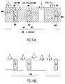
- FIG. 1Ais top view of the device showing a silicon line
- FIG. 1Bis a cross sectional view of cut 1 - 1 shown in FIG. 1A ;
- FIG. 1Cis a cross sectional view of cut 2 - 2 shown in FIG. 1A ;
- FIG. 2Ashows the substrate of FIG. 1A after epitaxial growth of etch stop and channel layers
- FIG. 2Cis a cross sectional view of cut 2 - 2 shown in FIG. 2A ;
- FIG. 3Ashows FIG. 2A with a mask opening for silicon line removal
- FIG. 3Bshows a cross sectional view of cut 2 - 2 shown in FIG. 3A ;
- FIG. 4Ashows FIG. 3A after the removal of any remaining portion of the silicon line and the etch stop layer
- FIG. 4Bshows a cross sectional view of the 2 - 2 cut shown in FIG. 4A ;
- FIG. 5shows the device of FIG. 4A after the formation of a second channel
- FIG. 6is a representational cross section of cut 2 - 2 shown in FIG. 5 ;
- FIG. 7shows the substrate of FIG. 6 after shallow trench isolation (STI) fill and polish
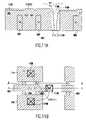
- FIG. 8Ais a representational cross section of cut 2 - 2 shown in FIG. 11B , after a polysilicon conductor (PC) resist mask is applied and etching;
- PCpolysilicon conductor
- FIG. 8Bis a representational cross section of cut 2 - 2 shown in FIG. 11 B, after a PC resist mask is applied;
- FIG. 9Ashows the substrate of FIG. 8A after gate dielectric growth or deposition, and gate conductor deposition
- FIG. 9Bshows the substrate of FIG. 8B after removal of the PC resist mask
- FIG. 10Ashows removal of STI and isolation implants in the substrate of FIG. 9A ;
- FIG. 11Ashows the completed device of FIG. 10A before contacts
- FIG. 11Bshows a top view of the completed device
- FIG. 12illustrates a technique of removing defective material due to excessive faceting.
- FIG. 1Athere is shown a top view of a starting silicon-on-insulator (SOI) substrate 100 .
- the substrate 100is comprised of a bulk substrate 106 , a buried oxide (BOX) 108 layer, and an active layer 110 .
- FIGS. 1B and 1Calso show an oxide pad film 102 and a nitride pad film 104 on active layer 110 .
- oxide pad film 102placed on top of the nitride pad film 104 .
- the active device layer 110is patterned to form edges 112 where the silicon channel will be formed.
- the width 113 of active layer 110which is used to form what will become the channel region, is not critical, other than it must be wide enough for masking and narrow enough to confine overetching, thereby providing an adequate, practical manufacturing tolerance. It is preferred that the silicon regions that will become the source 114 and drain 116 areas and contact areas 118 , 120 be formed during this stage in accordance with conventional processing techniques known to those skilled in the art.
- FIGS. 2A , 2 B and 2 Ccorrespond to FIGS. 1A , 1 B and 1 C, respectively, after epitaxial growth of etch stop 202 and subsequent epitaxial growth of the channel 204 .
- the etch stopbe comprised of Si(0.3)Ge(0.7)
- the epitaxially grown channelbe comprised of silicon or alloys of silicon with germanium and/or carbon. Alloys of silicon with other Group IV elements (particularly germanium and carbon) can be used to optimize the FET performance by adding strain to the channel and/or modifying the conduction and valence bands across the channel to alter the device threshold or improve carrier transport.
- etch stop 202 and channel 204prior to formation of etch stop 202 and channel 204 , a suitable cleaning process is used to remove a portion of the silicon 110 under the oxide pad film 104 .
- the width of the removed siliconshould be approximately equal to the combined width of the etch stop 202 and channel 204 .
- Non-selective epitaxial deposition of etch stop 202 and channel 204may be required if faceting is excessive, although selective deposition is preferred. It is preferred that the thickness of layer 202 be approximately 5 nm. Faceting will be highly dependent on details of epitaxial growth. Particularly with selective epitaxial growth, faceting may alter the thickness of the epitaxial regions as the edge of the opening is approached. Since the channel is projected to be very thin relative to the height of the growth, the area where the channel will be impacted is likely to be small. The allowed thickness before dislocations are created is sensitive to the Ge fraction and decreases quickly with increase in the Ge fraction (see A. Fischer and H. Kuhne, “Critical Dose for Strained Layer Configurations”, Phys. Stat. Sol. (a), 155, 141, 1996). Then, channel 204 is epitaxially grown, preferably in the range 5-50 nm.
- the bottom and top of channel 204may be defective. Particularly if the epitaxial layer is thin, the region is likely to be extremely small and may not be significant to the formation of the device. However, if it is necessary to remove these regions, two processes are available to do so at small but tolerable, degrade of device width control. Specifically, a spacer could be deposited similar to that of spacer 302 of FIG. 3B , but etched lower to uncover the top of the epitaxial region. After this spacer is formed, the buried oxide is etched underneath the spacer as shown on the left side of FIG. 12 . Alternatively, a thin composite spacer may be used. In this case, the bottom of the spacer are isotropically etched to uncover the top and bottom regions.
- the height of the spaceris determined by the undercut necessary to reach the epitaxial region at the bottom of the spacer, as shown on the right side of FIG. 12 .
- the spacersare removed selectively to the epitaxial regions and the buried oxide layer before proceeding to following processing steps. It should be noted that it is also possible to perform the procedure described above after the spacer shown in FIG. 4B is removed with the spacers of the above described procedure being removed before further processing.
- a maskis applied and positioned such that the mask opening 304 , shown in FIG. 3A , provides for removal of the exposed portion of silicon layer 110 and etch stop 202 within the mask opening 304 . It is preferred that the mask 304 be aligned as closely as possible to the channel 204 .
- the exposed silicon 110 within mask opening 304is then etched using an anisotropic etch.
- the exposed silicon 110 within mask opening 304is then etched. Since not all of the silicon 110 will be removed during this etch, the silicon layer 110 is also etched laterally, stopping on etch stop 202 (see K. D. Hobart, F. J. Kub, M. E. Twigg, G. G. Jernigan, P. E. Thompson, “Ultra-Cut: A Simple Technique for the Fabrication of SOI Substrates with Ultra-thin ( ⁇ 5 nm) Silicon Films”, Proc.
- KOHcan be utilized as an etchant, which has a selectivity of approximately 20:1 for Si:Si(O0.3)Ge(O0.7), whereas NH 4 OH is reported to have a selectivity of better than 100:1 for a 25% Ge film (see G. Wang et. al., “Highly Selective Chemical Etching of Si vs. Si(1-x)G(x) using NH40H solution, J. Electrochem. Soc., Vol. 144(3), March 1997, L37).
- etch stop 202is selectively etched to the channel 204 .
- the selectivity for HF:H 2 O 2 :CH 3 COOHis approximately 1000:1 for a 70% Ge film. Assuming a 10 nm etch, Si attack is therefore negligible.
- the selectivity for HNO 3 :H 2 O:HF (40:20:5)is approximately 25:1 selectivity for a 50% Ge film.
- the effective HF dilutionis approximately 12:1. Oxide attack will be significant, but can be controlled in accordance with conventional processing steps widely known to those skilled in the art.
- Etch rates for HNO 3 :H 2 O:HFare approximately 40 nm/min, suggesting very short exposures, and probably allowing further dilution for control. (see D. J.
- FIGS. 4A and 4Bcorrespond to FIGS. 3A and 3B , respectively, after the etching of active layer 110 and etch stop 202 .
- a trim maskcan be applied to remove undesired fins 402 in accordance with conventional processing techniques widely known to those skilled in the art.
- FIG. 5shows the device of FIG. 4A after the formation of a second channel 502 which, as will be readily recognized by those skilled in the art, can be formed by using the same processing steps as previously described for the first channel 204 .
- channels 204 and 502 of FIG. 5are shown, as well as an additional channel 602 that may be used to form another gate structure.
- substrate 100may comprise many channels in addition to shown channels 204 , 502 and 602 .
- the substrate 100thus comprises bulk substrate 102 , BOX layer 104 , and channels 204 , 502 and 602 .
- a standard STI fill 702is provided, which is preferably a silicon dioxide layer of approximately 300 to 500 nm thick.
- a silicon dioxide layerof approximately 300 to 500 nm thick.
- other suitable materials known to those skilled in the artmay also be used as a sacrificial film. It is preferred that the STI surface be planarized by polishing.
- FIG. 8Ais a representational cross-sectional cut of section 1 - 1 of FIG. 11B .
- FIG. 8Ais representational because polysilicon conductor (PC) resist 802 and STI fill 702 are present during fabrication in FIG. 8A , but are not present in corresponding region 114 of FIG. 11B .
- PCpolysilicon conductor
- STI fill 702is selectively etched relative to pad films 104 and down to the BOX layer 108 . It is preferred, but not required, that the etch also be selective relative to the BOX layer 108 .
- Pad films 104are then removed selectively to the STI fill layer 702 and BOX layer 104 .
- 9A and 10Ashow that the pad layers 104 could be left, if desired, to allow a thin gate dielectric 904 only on the sidewalls of channels 204 , 502 and 602 . It is preferred that there be approximately a 10:1 selectivity in each etch, which can be accomplished with known state of the art etches. If desired, well implants may optionally be introduced at this point. These implants would be done using highly angled implants, preferably in the range of 10 to 45 degrees, with each implant rotated at approximately 90 degrees relative to each other in order to fully dope the sidewalls of the diffusion. In order to avoid doping the surface layer of the diffusions more heavily than the sides, the implantation could be done before removing the pad films 104 in the exposed areas of PC resist 802 .
- FIG. 8Bis a representational cross-sectional cut of section 2 - 2 shown in FIG. 11B .
- FIG. 8Bis representational because PC resist mask 802 and STI fill 702 are present during fabrication in FIG. 8B , but are not shown in the region between the source 114 , drain 116 , and gate 902 in FIG. 11B .
- FIG. 8Bthus shows the selective placement of PC mask 802 during fabrication. This can be accomplished using standard pattern lithography techniques using a PC mask preferably composed of either photoresist or a hardmask.
- FIG. 9Ashows the substrate of FIG. 8A after gate dielectric growth 904 (e.g., SiO 2 ), and gate conductor 902 deposition.
- gate dielectric growth 904e.g., SiO 2
- gate conductor 902 depositione.g., SiO 2
- nitrided oxides, nitride/oxide composites, metal oxides (e.g., Al 2 O 3 , ZrSiO 4 , TiO 2 , Ta 2 O 5 , ZrO 2 , etc.), perovskites (e.g., (Ba, Sr)TiO 3 , La 2 O 3 ) and combinations of the abovecan also be used as the dielectric.
- Gate dielectric growth on each channel 204 , 502 and 602could be standard furnace or single-wafer chamber oxidations in accordance with conventional methods.
- FIG. 9Bshows FIG. 8B after removal of the PC resist mask 802 .
- the STI surface 904is cleaned in accordance with conventional techniques.
- FIG. 11Ashows the device of FIG. 10A after formation of silicide layer 1102 in accordance with conventional steps. Also in accordance with conventional steps, after the gate 902 is formed, spacers 1104 are formed and the diffusions are annealed, and a layer of highly conformal dielectric fill 1106 is deposited, and then polished to the top of the gate conductor. It is preferred that dielectric fill 1106 is a nitride layer followed by a doped glass. Because of the high aspect ratios, fill properties suggest a rapid-thermal CVD or a self-sputtering deposition using a high-density plasma-enhanced CVD technique. Typically, the dielectric glass includes phosphorus and/or boron, but it can also be undoped.
- FIG. 11Bshows a top view of the completed device.
- the source 114 and drain 116 regionare formed by implantation.
- Contacts 1106 , 1108 , 1110are added and back end of line (BEOL) processing is done in accordance with conventional steps.
- BEOLback end of line
Landscapes
- Thin Film Transistor (AREA)
- Insulated Gate Type Field-Effect Transistor (AREA)
- Metal-Oxide And Bipolar Metal-Oxide Semiconductor Integrated Circuits (AREA)
- Bipolar Transistors (AREA)
- Crystals, And After-Treatments Of Crystals (AREA)
- Mechanical Treatment Of Semiconductor (AREA)
Abstract
Description
Claims (12)
Priority Applications (1)
| Application Number | Priority Date | Filing Date | Title |
|---|---|---|---|
| US10/867,772US7265417B2 (en) | 2000-10-18 | 2004-06-16 | Method of fabricating semiconductor side wall fin |
Applications Claiming Priority (2)
| Application Number | Priority Date | Filing Date | Title |
|---|---|---|---|
| US09/691,353US7163864B1 (en) | 2000-10-18 | 2000-10-18 | Method of fabricating semiconductor side wall fin |
| US10/867,772US7265417B2 (en) | 2000-10-18 | 2004-06-16 | Method of fabricating semiconductor side wall fin |
Related Parent Applications (1)
| Application Number | Title | Priority Date | Filing Date |
|---|---|---|---|
| US09/691,353DivisionUS7163864B1 (en) | 2000-10-18 | 2000-10-18 | Method of fabricating semiconductor side wall fin |
Publications (2)
| Publication Number | Publication Date |
|---|---|
| US20050001216A1 US20050001216A1 (en) | 2005-01-06 |
| US7265417B2true US7265417B2 (en) | 2007-09-04 |
Family
ID=24776208
Family Applications (3)
| Application Number | Title | Priority Date | Filing Date |
|---|---|---|---|
| US09/691,353Expired - LifetimeUS7163864B1 (en) | 2000-10-18 | 2000-10-18 | Method of fabricating semiconductor side wall fin |
| US10/867,772Expired - Fee RelatedUS7265417B2 (en) | 2000-10-18 | 2004-06-16 | Method of fabricating semiconductor side wall fin |
| US11/495,518Expired - Fee RelatedUS7361556B2 (en) | 2000-10-18 | 2006-07-31 | Method of fabricating semiconductor side wall fin |
Family Applications Before (1)
| Application Number | Title | Priority Date | Filing Date |
|---|---|---|---|
| US09/691,353Expired - LifetimeUS7163864B1 (en) | 2000-10-18 | 2000-10-18 | Method of fabricating semiconductor side wall fin |
Family Applications After (1)
| Application Number | Title | Priority Date | Filing Date |
|---|---|---|---|
| US11/495,518Expired - Fee RelatedUS7361556B2 (en) | 2000-10-18 | 2006-07-31 | Method of fabricating semiconductor side wall fin |
Country Status (9)
| Country | Link |
|---|---|
| US (3) | US7163864B1 (en) |
| EP (1) | EP1202335B1 (en) |
| JP (1) | JP4071951B2 (en) |
| KR (1) | KR100444095B1 (en) |
| CN (1) | CN100530567C (en) |
| AT (1) | ATE426246T1 (en) |
| DE (1) | DE60138000D1 (en) |
| SG (1) | SG97204A1 (en) |
| TW (1) | TW526564B (en) |
Cited By (6)
| Publication number | Priority date | Publication date | Assignee | Title |
|---|---|---|---|---|
| US20060220133A1 (en)* | 2003-04-29 | 2006-10-05 | Yee-Chia Yeo | Doping of semiconductor fin devices |
| US20060255410A1 (en)* | 2004-04-12 | 2006-11-16 | Kerry Bernstein | FinFET TRANSISTOR AND CIRCUIT |
| US20080206934A1 (en)* | 2007-02-23 | 2008-08-28 | Jones Robert E | Forming semiconductor fins using a sacrificial fin |
| US7855105B1 (en)* | 2009-06-18 | 2010-12-21 | International Business Machines Corporation | Planar and non-planar CMOS devices with multiple tuned threshold voltages |
| US20110129978A1 (en)* | 2009-12-01 | 2011-06-02 | Kangguo Cheng | Method and structure for forming finfets with multiple doping regions on a same chip |
| US8338256B2 (en) | 2010-07-08 | 2012-12-25 | International Business Machines Corporation | Multi-gate transistor having sidewall contacts |
Families Citing this family (99)
| Publication number | Priority date | Publication date | Assignee | Title |
|---|---|---|---|---|
| US7358121B2 (en) | 2002-08-23 | 2008-04-15 | Intel Corporation | Tri-gate devices and methods of fabrication |
| US6800910B2 (en)* | 2002-09-30 | 2004-10-05 | Advanced Micro Devices, Inc. | FinFET device incorporating strained silicon in the channel region |
| JP4546021B2 (en)* | 2002-10-02 | 2010-09-15 | ルネサスエレクトロニクス株式会社 | Insulated gate field effect transistor and semiconductor device |
| KR100474850B1 (en)* | 2002-11-15 | 2005-03-11 | 삼성전자주식회사 | Silicon/Oxide/Nitride/Oxide/Silicon nonvolatile memory with vertical channel and Fabricating method thereof |
| US6709982B1 (en) | 2002-11-26 | 2004-03-23 | Advanced Micro Devices, Inc. | Double spacer FinFET formation |
| US6720619B1 (en)* | 2002-12-13 | 2004-04-13 | Taiwan Semiconductor Manufacturing Company, Ltd. | Semiconductor-on-insulator chip incorporating partially-depleted, fully-depleted, and multiple-gate devices |
| US6762483B1 (en)* | 2003-01-23 | 2004-07-13 | Advanced Micro Devices, Inc. | Narrow fin FinFET |
| US6803631B2 (en)* | 2003-01-23 | 2004-10-12 | Advanced Micro Devices, Inc. | Strained channel finfet |
| WO2004073044A2 (en) | 2003-02-13 | 2004-08-26 | Massachusetts Institute Of Technology | Finfet device and method to make same |
| KR100483425B1 (en)* | 2003-03-17 | 2005-04-14 | 삼성전자주식회사 | Semiconductor device and method for manufacturing the same |
| US6762448B1 (en)* | 2003-04-03 | 2004-07-13 | Advanced Micro Devices, Inc. | FinFET device with multiple fin structures |
| JP4632046B2 (en)* | 2003-04-09 | 2011-02-16 | 日本電気株式会社 | Vertical MISFET semiconductor device having high mobility silicon channel |
| US6909186B2 (en)* | 2003-05-01 | 2005-06-21 | International Business Machines Corporation | High performance FET devices and methods therefor |
| JP4105044B2 (en) | 2003-06-13 | 2008-06-18 | 株式会社東芝 | Field effect transistor |
| US6894326B2 (en)* | 2003-06-25 | 2005-05-17 | International Business Machines Corporation | High-density finFET integration scheme |
| US7456476B2 (en) | 2003-06-27 | 2008-11-25 | Intel Corporation | Nonplanar semiconductor device with partially or fully wrapped around gate electrode and methods of fabrication |
| US6909151B2 (en) | 2003-06-27 | 2005-06-21 | Intel Corporation | Nonplanar device with stress incorporation layer and method of fabrication |
| US6716686B1 (en) | 2003-07-08 | 2004-04-06 | Advanced Micro Devices, Inc. | Method for forming channels in a finfet device |
| KR100973092B1 (en) | 2003-07-21 | 2010-07-29 | 매그나칩 반도체 유한회사 | Fabrication method of vertical MOS capacitor using silicon on insulator wafer |
| US7013447B2 (en)* | 2003-07-22 | 2006-03-14 | Freescale Semiconductor, Inc. | Method for converting a planar transistor design to a vertical double gate transistor design |
| US7355253B2 (en) | 2003-08-22 | 2008-04-08 | International Business Machines Corporation | Strained-channel Fin field effect transistor (FET) with a uniform channel thickness and separate gates |
| US6946377B2 (en)* | 2003-10-29 | 2005-09-20 | Texas Instruments Incorporated | Multiple-gate MOSFET device with lithography independent silicon body thickness and methods for fabricating the same |
| US7029958B2 (en) | 2003-11-04 | 2006-04-18 | Advanced Micro Devices, Inc. | Self aligned damascene gate |
| US7498225B1 (en) | 2003-12-04 | 2009-03-03 | Advanced Micro Devices, Inc. | Systems and methods for forming multiple fin structures using metal-induced-crystallization |
| US7388258B2 (en)* | 2003-12-10 | 2008-06-17 | International Business Machines Corporation | Sectional field effect devices |
| US7105390B2 (en) | 2003-12-30 | 2006-09-12 | Intel Corporation | Nonplanar transistors with metal gate electrodes |
| US7268058B2 (en) | 2004-01-16 | 2007-09-11 | Intel Corporation | Tri-gate transistors and methods to fabricate same |
| US7154118B2 (en)* | 2004-03-31 | 2006-12-26 | Intel Corporation | Bulk non-planar transistor having strained enhanced mobility and methods of fabrication |
| US7579280B2 (en) | 2004-06-01 | 2009-08-25 | Intel Corporation | Method of patterning a film |
| US7042009B2 (en) | 2004-06-30 | 2006-05-09 | Intel Corporation | High mobility tri-gate devices and methods of fabrication |
| US7348284B2 (en) | 2004-08-10 | 2008-03-25 | Intel Corporation | Non-planar pMOS structure with a strained channel region and an integrated strained CMOS flow |
| KR100555573B1 (en) | 2004-09-10 | 2006-03-03 | 삼성전자주식회사 | Semiconductor device having a junction region extended by SEB film and method for manufacturing same |
| US7422946B2 (en) | 2004-09-29 | 2008-09-09 | Intel Corporation | Independently accessed double-gate and tri-gate transistors in same process flow |
| US7332439B2 (en) | 2004-09-29 | 2008-02-19 | Intel Corporation | Metal gate transistors with epitaxial source and drain regions |
| US7361958B2 (en) | 2004-09-30 | 2008-04-22 | Intel Corporation | Nonplanar transistors with metal gate electrodes |
| US20060086977A1 (en) | 2004-10-25 | 2006-04-27 | Uday Shah | Nonplanar device with thinned lower body portion and method of fabrication |
| US7193279B2 (en) | 2005-01-18 | 2007-03-20 | Intel Corporation | Non-planar MOS structure with a strained channel region |
| JP2008529295A (en)* | 2005-01-28 | 2008-07-31 | エヌエックスピー ビー ヴィ | Method for manufacturing a dual gate FET |
| US7518196B2 (en) | 2005-02-23 | 2009-04-14 | Intel Corporation | Field effect transistor with narrow bandgap source and drain regions and method of fabrication |
| US20060202266A1 (en) | 2005-03-14 | 2006-09-14 | Marko Radosavljevic | Field effect transistor with metal source/drain regions |
| JP4987244B2 (en)* | 2005-04-28 | 2012-07-25 | 株式会社東芝 | Manufacturing method of semiconductor device |
| US9153645B2 (en) | 2005-05-17 | 2015-10-06 | Taiwan Semiconductor Manufacturing Company, Ltd. | Lattice-mismatched semiconductor structures with reduced dislocation defect densities and related methods for device fabrication |
| US8324660B2 (en) | 2005-05-17 | 2012-12-04 | Taiwan Semiconductor Manufacturing Company, Ltd. | Lattice-mismatched semiconductor structures with reduced dislocation defect densities and related methods for device fabrication |
| US7858481B2 (en) | 2005-06-15 | 2010-12-28 | Intel Corporation | Method for fabricating transistor with thinned channel |
| US7547637B2 (en) | 2005-06-21 | 2009-06-16 | Intel Corporation | Methods for patterning a semiconductor film |
| US7902598B2 (en) | 2005-06-24 | 2011-03-08 | Micron Technology, Inc. | Two-sided surround access transistor for a 4.5F2 DRAM cell |
| US7279375B2 (en) | 2005-06-30 | 2007-10-09 | Intel Corporation | Block contact architectures for nanoscale channel transistors |
| US7402875B2 (en) | 2005-08-17 | 2008-07-22 | Intel Corporation | Lateral undercut of metal gate in SOI device |
| US7339241B2 (en)* | 2005-08-31 | 2008-03-04 | Freescale Semiconductor, Inc. | FinFET structure with contacts |
| US20070090416A1 (en) | 2005-09-28 | 2007-04-26 | Doyle Brian S | CMOS devices with a single work function gate electrode and method of fabrication |
| US7479421B2 (en) | 2005-09-28 | 2009-01-20 | Intel Corporation | Process for integrating planar and non-planar CMOS transistors on a bulk substrate and article made thereby |
| US7485503B2 (en) | 2005-11-30 | 2009-02-03 | Intel Corporation | Dielectric interface for group III-V semiconductor device |
| US7396711B2 (en) | 2005-12-27 | 2008-07-08 | Intel Corporation | Method of fabricating a multi-cornered film |
| DE102006001680B3 (en) | 2006-01-12 | 2007-08-09 | Infineon Technologies Ag | Manufacturing method for a FinFET transistor arrangement and corresponding FinFET transistor arrangement |
| US7446001B2 (en)* | 2006-02-08 | 2008-11-04 | Freescale Semiconductors, Inc. | Method for forming a semiconductor-on-insulator (SOI) body-contacted device with a portion of drain region removed |
| WO2007112066A2 (en) | 2006-03-24 | 2007-10-04 | Amberwave Systems Corporation | Lattice-mismatched semiconductor structures and related methods for device fabrication |
| US7449373B2 (en) | 2006-03-31 | 2008-11-11 | Intel Corporation | Method of ion implanting for tri-gate devices |
| US7670928B2 (en) | 2006-06-14 | 2010-03-02 | Intel Corporation | Ultra-thin oxide bonding for S1 to S1 dual orientation bonding |
| US8143646B2 (en) | 2006-08-02 | 2012-03-27 | Intel Corporation | Stacking fault and twin blocking barrier for integrating III-V on Si |
| EP1892765A1 (en)* | 2006-08-23 | 2008-02-27 | INTERUNIVERSITAIR MICROELEKTRONICA CENTRUM vzw (IMEC) | Method for doping a fin-based semiconductor device |
| EP1916717A3 (en)* | 2006-08-23 | 2010-12-22 | Imec | Method for doping a fin-based semiconductor device |
| US8173551B2 (en) | 2006-09-07 | 2012-05-08 | Taiwan Semiconductor Manufacturing Co., Ltd. | Defect reduction using aspect ratio trapping |
| WO2008039534A2 (en) | 2006-09-27 | 2008-04-03 | Amberwave Systems Corporation | Quantum tunneling devices and circuits with lattice- mismatched semiconductor structures |
| US8502263B2 (en)* | 2006-10-19 | 2013-08-06 | Taiwan Semiconductor Manufacturing Company, Ltd. | Light-emitter-based devices with lattice-mismatched semiconductor structures |
| KR100827696B1 (en)* | 2006-12-08 | 2008-05-07 | 삼성전자주식회사 | Transistor layout structure and transistor size adjustment method that can adjust size without changing active area |
| JP4866918B2 (en)* | 2007-01-22 | 2012-02-01 | パナソニック株式会社 | Semiconductor device |
| US7838948B2 (en)* | 2007-01-30 | 2010-11-23 | Infineon Technologies Ag | Fin interconnects for multigate FET circuit blocks |
| US8304805B2 (en)* | 2009-01-09 | 2012-11-06 | Taiwan Semiconductor Manufacturing Company, Ltd. | Semiconductor diodes fabricated by aspect ratio trapping with coalesced films |
| WO2008124154A2 (en) | 2007-04-09 | 2008-10-16 | Amberwave Systems Corporation | Photovoltaics on silicon |
| US8237151B2 (en) | 2009-01-09 | 2012-08-07 | Taiwan Semiconductor Manufacturing Company, Ltd. | Diode-based devices and methods for making the same |
| US7825328B2 (en) | 2007-04-09 | 2010-11-02 | Taiwan Semiconductor Manufacturing Company, Ltd. | Nitride-based multi-junction solar cell modules and methods for making the same |
| US7709390B2 (en)* | 2007-05-31 | 2010-05-04 | Micron Technology, Inc. | Methods of isolating array features during pitch doubling processes and semiconductor device structures having isolated array features |
| US8329541B2 (en) | 2007-06-15 | 2012-12-11 | Taiwan Semiconductor Manufacturing Company, Ltd. | InP-based transistor fabrication |
| JP5011011B2 (en)* | 2007-07-12 | 2012-08-29 | 株式会社東芝 | Manufacturing method of semiconductor device |
| JP2010538495A (en) | 2007-09-07 | 2010-12-09 | アンバーウェーブ・システムズ・コーポレーション | Multi-junction solar cell |
| EP2229690B1 (en)* | 2007-09-26 | 2011-04-20 | STMicroelectronics (Crolles 2) SAS | Process for forming a wire portion in an integrated electronic circuit |
| JP2008160145A (en)* | 2008-02-04 | 2008-07-10 | Renesas Technology Corp | Insulated gate field effect transistor and semiconductor device |
| US8183667B2 (en) | 2008-06-03 | 2012-05-22 | Taiwan Semiconductor Manufacturing Co., Ltd. | Epitaxial growth of crystalline material |
| US8362566B2 (en) | 2008-06-23 | 2013-01-29 | Intel Corporation | Stress in trigate devices using complimentary gate fill materials |
| US8274097B2 (en) | 2008-07-01 | 2012-09-25 | Taiwan Semiconductor Manufacturing Company, Ltd. | Reduction of edge effects from aspect ratio trapping |
| US8981427B2 (en) | 2008-07-15 | 2015-03-17 | Taiwan Semiconductor Manufacturing Company, Ltd. | Polishing of small composite semiconductor materials |
| US20100072515A1 (en)* | 2008-09-19 | 2010-03-25 | Amberwave Systems Corporation | Fabrication and structures of crystalline material |
| EP2335273A4 (en) | 2008-09-19 | 2012-01-25 | Taiwan Semiconductor Mfg | FORMATION OF DEVICES BY GROWTH OF EPITAXIAL LAYERS |
| US8253211B2 (en)* | 2008-09-24 | 2012-08-28 | Taiwan Semiconductor Manufacturing Company, Ltd. | Semiconductor sensor structures with reduced dislocation defect densities |
| US8629446B2 (en) | 2009-04-02 | 2014-01-14 | Taiwan Semiconductor Manufacturing Company, Ltd. | Devices formed from a non-polar plane of a crystalline material and method of making the same |
| JP5714831B2 (en)* | 2010-03-18 | 2015-05-07 | ルネサスエレクトロニクス株式会社 | Manufacturing method of semiconductor device |
| US8298913B2 (en)* | 2010-10-12 | 2012-10-30 | International Business Machines Corporation | Devices with gate-to-gate isolation structures and methods of manufacture |
| US8404560B2 (en)* | 2010-10-12 | 2013-03-26 | International Business Machines Corporation | Devices with gate-to-gate isolation structures and methods of manufacture |
| US8455330B2 (en) | 2010-10-12 | 2013-06-04 | International Business Machines Corporation | Devices with gate-to-gate isolation structures and methods of manufacture |
| JP5713837B2 (en)* | 2011-08-10 | 2015-05-07 | 株式会社東芝 | Manufacturing method of semiconductor device |
| FR2995720B1 (en)* | 2012-09-18 | 2014-10-24 | Commissariat Energie Atomique | METHOD FOR MAKING INDEPENDENT GRID DOUBLE-FIELD FIELD EFFECT DEVICE |
| JP6033714B2 (en)* | 2013-03-11 | 2016-11-30 | 株式会社日立製作所 | Semiconductor optical device and manufacturing method thereof |
| US8895395B1 (en) | 2013-06-06 | 2014-11-25 | International Business Machines Corporation | Reduced resistance SiGe FinFET devices and method of forming same |
| CN105321820B (en)* | 2014-07-08 | 2018-09-14 | 台湾积体电路制造股份有限公司 | Layout designs are changed to reduce turning sphering effect by OPC |
| KR102290793B1 (en) | 2014-12-18 | 2021-08-19 | 삼성전자주식회사 | Semiconductor device, methods of forming patterns for semiconductor device, and methods of manufacturing semiconductor devices |
| US9704859B1 (en) | 2016-05-06 | 2017-07-11 | International Business Machines Corporation | Forming semiconductor fins with self-aligned patterning |
| US10157745B2 (en) | 2016-06-29 | 2018-12-18 | International Business Machines Corporation | High aspect ratio gates |
| US10276442B1 (en) | 2018-05-30 | 2019-04-30 | Globalfoundries Inc. | Wrap-around contacts formed with multiple silicide layers |
| US20240105793A1 (en)* | 2022-09-26 | 2024-03-28 | Psemi Corporation | Transistors designed with reduced leakage |
Citations (28)
| Publication number | Priority date | Publication date | Assignee | Title |
|---|---|---|---|---|
| US3876480A (en) | 1972-08-28 | 1975-04-08 | Motorola Inc | Method of manufacturing high speed, isolated integrated circuit |
| US4716128A (en) | 1986-12-10 | 1987-12-29 | General Motors Corporation | Method of fabricating silicon-on-insulator like devices |
| US4996574A (en) | 1988-07-01 | 1991-02-26 | Fujitsu Limited | MIS transistor structure for increasing conductance between source and drain regions |
| US5049521A (en) | 1989-11-30 | 1991-09-17 | Silicon General, Inc. | Method for forming dielectrically isolated semiconductor devices with contact to the wafer substrate |
| US5346834A (en) | 1988-11-21 | 1994-09-13 | Hitachi, Ltd. | Method for manufacturing a semiconductor device and a semiconductor memory device |
| US5391506A (en) | 1992-01-31 | 1995-02-21 | Kawasaki Steel Corporation | Manufacturing method for semiconductor devices with source/drain formed in substrate projection. |
| US5494837A (en) | 1994-09-27 | 1996-02-27 | Purdue Research Foundation | Method of forming semiconductor-on-insulator electronic devices by growing monocrystalline semiconducting regions from trench sidewalls |
| US5545586A (en) | 1990-11-27 | 1996-08-13 | Nec Corporation | Method of making a transistor having easily controllable impurity profile |
| US5581101A (en) | 1995-01-03 | 1996-12-03 | International Business Machines Corporation | FET and/or bipolar devices formed in thin vertical silicon on insulator (SOI) structures |
| US5593928A (en) | 1993-11-30 | 1997-01-14 | Lg Semicon Co., Ltd. | Method of making a semiconductor device having floating source and drain regions |
| US5612230A (en) | 1991-04-16 | 1997-03-18 | Canon Kabushiki Kaisha | Process for manufacturing a semiconductor device by applying a non-single-crystalline material on a sidewall inside of an opening portion for growing a single-crystalline semiconductor body |
| DE19633914C1 (en) | 1996-04-26 | 1997-08-07 | Mitsubishi Electric Corp | Thin film transistor device |
| US5675164A (en) | 1995-06-07 | 1997-10-07 | International Business Machines Corporation | High performance multi-mesa field effect transistor |
| US5773331A (en) | 1996-12-17 | 1998-06-30 | International Business Machines Corporation | Method for making single and double gate field effect transistors with sidewall source-drain contacts |
| US5885876A (en)* | 1996-02-07 | 1999-03-23 | Thunderbird Technologies, Inc. | Methods of fabricating short channel fermi-threshold field effect transistors including drain field termination region |
| JPH11233774A (en) | 1997-12-17 | 1999-08-27 | Lg Semicon Co Ltd | Thin film transistor and method of manufacturing the same |
| JPH11251579A (en) | 1998-01-15 | 1999-09-17 | Internatl Business Mach Corp <Ibm> | Field effect transistor and method of manufacturing the same |
| WO2000030181A2 (en) | 1998-11-18 | 2000-05-25 | Infineon Technologies Ag | Field effect-controlled transistor and method for producing the same |
| US6118161A (en) | 1997-04-30 | 2000-09-12 | Texas Instruments Incorporated | Self-aligned trenched-channel lateral-current-flow transistor |
| US6310367B1 (en)* | 1999-02-22 | 2001-10-30 | Kabushiki Kaisha Toshiba | MOS transistor having a tensile-strained SI layer and a compressive-strained SI-GE layer |
| US6383892B1 (en)* | 1998-08-06 | 2002-05-07 | International Business Machines Corporation | Double silicon-on-insulator device and method thereof |
| US6458662B1 (en)* | 2001-04-04 | 2002-10-01 | Advanced Micro Devices, Inc. | Method of fabricating a semiconductor device having an asymmetrical dual-gate silicon-germanium (SiGe) channel MOSFET and a device thereby formed |
| US6483156B1 (en)* | 2000-03-16 | 2002-11-19 | International Business Machines Corporation | Double planar gated SOI MOSFET structure |
| US20030006410A1 (en)* | 2000-03-01 | 2003-01-09 | Brian Doyle | Quantum wire gate device and method of making same |
| US20030178670A1 (en)* | 2002-03-19 | 2003-09-25 | International Business Machines Corporation | Finfet CMOS with NVRAM capability |
| US6768158B2 (en)* | 2001-09-04 | 2004-07-27 | Korea Advanced Institute Of Science And Technology | Flash memory element and manufacturing method thereof |
| US7064019B2 (en)* | 2001-12-14 | 2006-06-20 | International Business Machines Corporation | Implanted asymmetric doped polysilicon gate FinFET |
| US7192876B2 (en)* | 2003-05-22 | 2007-03-20 | Freescale Semiconductor, Inc. | Transistor with independent gate structures |
Family Cites Families (18)
| Publication number | Priority date | Publication date | Assignee | Title |
|---|---|---|---|---|
| FR2645345A1 (en)* | 1989-03-31 | 1990-10-05 | Thomson Csf | METHOD FOR DIRECT MODULATION OF THE COMPOSITION OR DOPING OF SEMICONDUCTORS, IN PARTICULAR FOR THE PRODUCTION OF ELECTRONIC MONOLITHIC COMPONENTS OF THE PLANAR TYPE, USE AND CORRESPONDING PRODUCTS |
| FR2666172B1 (en)* | 1990-08-24 | 1997-05-16 | Thomson Csf | POWER TRANSISTOR AND METHOD FOR PRODUCING THE SAME. |
| JPH05121321A (en)* | 1991-10-25 | 1993-05-18 | Rohm Co Ltd | Silicon crystal growth method |
| US5273921A (en)* | 1991-12-27 | 1993-12-28 | Purdue Research Foundation | Methods for fabricating a dual-gated semiconductor-on-insulator field effect transistor |
| US5365097A (en)* | 1992-10-05 | 1994-11-15 | International Business Machines Corporation | Vertical epitaxial SOI transistor, memory cell and fabrication methods |
| US5346934A (en)* | 1992-12-21 | 1994-09-13 | Chriss Henry T | Footwear additive made from recycled materials |
| EP0937918A3 (en)* | 1993-07-29 | 1999-09-01 | Fuji Jukogyo Kabushiki Kaisha | Range selector failure detecting system and method for automatic transmission |
| DE4441901C2 (en)* | 1994-11-24 | 1998-07-02 | Siemens Ag | MOSFET on SOI substrate and method for its production |
| US5757038A (en)* | 1995-11-06 | 1998-05-26 | International Business Machines Corporation | Self-aligned dual gate MOSFET with an ultranarrow channel |
| DE19548058C2 (en)* | 1995-12-21 | 1997-11-20 | Siemens Ag | Method of manufacturing a MOS transistor |
| KR100281110B1 (en)* | 1997-12-15 | 2001-03-02 | 김영환 | Semiconductor device and method for fabricating the same |
| US6040605A (en)* | 1998-01-28 | 2000-03-21 | Hitachi, Ltd. | Semiconductor memory device |
| US6365465B1 (en)* | 1999-03-19 | 2002-04-02 | International Business Machines Corporation | Self-aligned double-gate MOSFET by selective epitaxy and silicon wafer bonding techniques |
| US6479847B2 (en)* | 1999-05-07 | 2002-11-12 | International Business Machines Corporation | Method for complementary oxide transistor fabrication |
| US6563131B1 (en)* | 2000-06-02 | 2003-05-13 | International Business Machines Corporation | Method and structure of a dual/wrap-around gate field effect transistor |
| US6441433B1 (en)* | 2001-04-02 | 2002-08-27 | Advanced Micro Devices, Inc. | Method of making a multi-thickness silicide SOI device |
| US6833569B2 (en)* | 2002-12-23 | 2004-12-21 | International Business Machines Corporation | Self-aligned planar double-gate process by amorphization |
| US7355253B2 (en)* | 2003-08-22 | 2008-04-08 | International Business Machines Corporation | Strained-channel Fin field effect transistor (FET) with a uniform channel thickness and separate gates |
- 2000
- 2000-10-18USUS09/691,353patent/US7163864B1/ennot_activeExpired - Lifetime
- 2001
- 2001-10-05KRKR10-2001-0061318Apatent/KR100444095B1/ennot_activeExpired - Fee Related
- 2001-10-12SGSG200106328Apatent/SG97204A1/enunknown
- 2001-10-15DEDE60138000Tpatent/DE60138000D1/ennot_activeExpired - Lifetime
- 2001-10-15TWTW090125391Apatent/TW526564B/ennot_activeIP Right Cessation
- 2001-10-15ATAT01308767Tpatent/ATE426246T1/ennot_activeIP Right Cessation
- 2001-10-15EPEP01308767Apatent/EP1202335B1/ennot_activeExpired - Lifetime
- 2001-10-17JPJP2001319845Apatent/JP4071951B2/ennot_activeExpired - Fee Related
- 2001-10-18CNCNB011357991Apatent/CN100530567C/ennot_activeExpired - Fee Related
- 2004
- 2004-06-16USUS10/867,772patent/US7265417B2/ennot_activeExpired - Fee Related
- 2006
- 2006-07-31USUS11/495,518patent/US7361556B2/ennot_activeExpired - Fee Related
Patent Citations (32)
| Publication number | Priority date | Publication date | Assignee | Title |
|---|---|---|---|---|
| US3876480A (en) | 1972-08-28 | 1975-04-08 | Motorola Inc | Method of manufacturing high speed, isolated integrated circuit |
| US4716128A (en) | 1986-12-10 | 1987-12-29 | General Motors Corporation | Method of fabricating silicon-on-insulator like devices |
| US4996574A (en) | 1988-07-01 | 1991-02-26 | Fujitsu Limited | MIS transistor structure for increasing conductance between source and drain regions |
| US5466621A (en) | 1988-11-21 | 1995-11-14 | Hitachi, Ltd. | Method of manufacturing a semiconductor device having silicon islands |
| US5346834A (en) | 1988-11-21 | 1994-09-13 | Hitachi, Ltd. | Method for manufacturing a semiconductor device and a semiconductor memory device |
| US5049521A (en) | 1989-11-30 | 1991-09-17 | Silicon General, Inc. | Method for forming dielectrically isolated semiconductor devices with contact to the wafer substrate |
| US5545586A (en) | 1990-11-27 | 1996-08-13 | Nec Corporation | Method of making a transistor having easily controllable impurity profile |
| US5612230A (en) | 1991-04-16 | 1997-03-18 | Canon Kabushiki Kaisha | Process for manufacturing a semiconductor device by applying a non-single-crystalline material on a sidewall inside of an opening portion for growing a single-crystalline semiconductor body |
| US5391506A (en) | 1992-01-31 | 1995-02-21 | Kawasaki Steel Corporation | Manufacturing method for semiconductor devices with source/drain formed in substrate projection. |
| US5593928A (en) | 1993-11-30 | 1997-01-14 | Lg Semicon Co., Ltd. | Method of making a semiconductor device having floating source and drain regions |
| US5494837A (en) | 1994-09-27 | 1996-02-27 | Purdue Research Foundation | Method of forming semiconductor-on-insulator electronic devices by growing monocrystalline semiconducting regions from trench sidewalls |
| US5581101A (en) | 1995-01-03 | 1996-12-03 | International Business Machines Corporation | FET and/or bipolar devices formed in thin vertical silicon on insulator (SOI) structures |
| US5675164A (en) | 1995-06-07 | 1997-10-07 | International Business Machines Corporation | High performance multi-mesa field effect transistor |
| US5885876A (en)* | 1996-02-07 | 1999-03-23 | Thunderbird Technologies, Inc. | Methods of fabricating short channel fermi-threshold field effect transistors including drain field termination region |
| DE19633914C1 (en) | 1996-04-26 | 1997-08-07 | Mitsubishi Electric Corp | Thin film transistor device |
| US5773331A (en) | 1996-12-17 | 1998-06-30 | International Business Machines Corporation | Method for making single and double gate field effect transistors with sidewall source-drain contacts |
| US6118161A (en) | 1997-04-30 | 2000-09-12 | Texas Instruments Incorporated | Self-aligned trenched-channel lateral-current-flow transistor |
| JPH11233774A (en) | 1997-12-17 | 1999-08-27 | Lg Semicon Co Ltd | Thin film transistor and method of manufacturing the same |
| US6165829A (en) | 1997-12-17 | 2000-12-26 | Hyundai Electronics Industries Co., Ltd. | Thin film transistor and fabrication method therefor |
| JPH11251579A (en) | 1998-01-15 | 1999-09-17 | Internatl Business Mach Corp <Ibm> | Field effect transistor and method of manufacturing the same |
| US6177299B1 (en) | 1998-01-15 | 2001-01-23 | International Business Machines Corporation | Transistor having substantially isolated body and method of making the same |
| US6383892B1 (en)* | 1998-08-06 | 2002-05-07 | International Business Machines Corporation | Double silicon-on-insulator device and method thereof |
| WO2000030181A2 (en) | 1998-11-18 | 2000-05-25 | Infineon Technologies Ag | Field effect-controlled transistor and method for producing the same |
| US6310367B1 (en)* | 1999-02-22 | 2001-10-30 | Kabushiki Kaisha Toshiba | MOS transistor having a tensile-strained SI layer and a compressive-strained SI-GE layer |
| US20030006410A1 (en)* | 2000-03-01 | 2003-01-09 | Brian Doyle | Quantum wire gate device and method of making same |
| US6660596B2 (en)* | 2000-03-16 | 2003-12-09 | International Business Machines Corporation | Double planar gated SOI MOSFET structure |
| US6483156B1 (en)* | 2000-03-16 | 2002-11-19 | International Business Machines Corporation | Double planar gated SOI MOSFET structure |
| US6458662B1 (en)* | 2001-04-04 | 2002-10-01 | Advanced Micro Devices, Inc. | Method of fabricating a semiconductor device having an asymmetrical dual-gate silicon-germanium (SiGe) channel MOSFET and a device thereby formed |
| US6768158B2 (en)* | 2001-09-04 | 2004-07-27 | Korea Advanced Institute Of Science And Technology | Flash memory element and manufacturing method thereof |
| US7064019B2 (en)* | 2001-12-14 | 2006-06-20 | International Business Machines Corporation | Implanted asymmetric doped polysilicon gate FinFET |
| US20030178670A1 (en)* | 2002-03-19 | 2003-09-25 | International Business Machines Corporation | Finfet CMOS with NVRAM capability |
| US7192876B2 (en)* | 2003-05-22 | 2007-03-20 | Freescale Semiconductor, Inc. | Transistor with independent gate structures |
Non-Patent Citations (10)
Cited By (20)
| Publication number | Priority date | Publication date | Assignee | Title |
|---|---|---|---|---|
| US20060234431A1 (en)* | 2003-04-29 | 2006-10-19 | Yee-Chia Yeo | Doping of semiconductor fin devices |
| US20060220133A1 (en)* | 2003-04-29 | 2006-10-05 | Yee-Chia Yeo | Doping of semiconductor fin devices |
| US7701008B2 (en)* | 2003-04-29 | 2010-04-20 | Taiwan Semiconductor Manufacturing Company, Ltd. | Doping of semiconductor fin devices |
| US20100176424A1 (en)* | 2003-04-29 | 2010-07-15 | Taiwan Semiconductor Manufacturing Company, Ltd. | Doping of Semiconductor Fin Devices |
| US8790970B2 (en) | 2003-04-29 | 2014-07-29 | Taiwan Semiconductor Manufacturing Company, Ltd. | Doping of semiconductor fin devices |
| US8053839B2 (en) | 2003-04-29 | 2011-11-08 | Taiwan Semiconductor Manufacturing Company, Ltd. | Doping of semiconductor fin devices |
| US7964466B2 (en) | 2004-04-12 | 2011-06-21 | International Business Machines Corporation | FinFET transistor and circuit |
| US20060255410A1 (en)* | 2004-04-12 | 2006-11-16 | Kerry Bernstein | FinFET TRANSISTOR AND CIRCUIT |
| US20080099795A1 (en)* | 2004-04-12 | 2008-05-01 | Kerry Bernstein | FinFET TRANSISTOR AND CIRCUIT |
| US7368355B2 (en)* | 2004-04-12 | 2008-05-06 | International Business Machines Corporation | FinFET transistor and circuit |
| US20100203689A1 (en)* | 2004-04-12 | 2010-08-12 | International Business Machines Corporation | finFET TRANSISTOR AND CIRCUIT |
| US7777276B2 (en)* | 2004-04-12 | 2010-08-17 | International Business Machines Corporation | FinFET transistor and circuit |
| US20080206934A1 (en)* | 2007-02-23 | 2008-08-28 | Jones Robert E | Forming semiconductor fins using a sacrificial fin |
| US7772048B2 (en)* | 2007-02-23 | 2010-08-10 | Freescale Semiconductor, Inc. | Forming semiconductor fins using a sacrificial fin |
| US20100320545A1 (en)* | 2009-06-18 | 2010-12-23 | International Business Machines Corporation | Planar and non-planar cmos devices with multiple tuned threshold voltages |
| US7855105B1 (en)* | 2009-06-18 | 2010-12-21 | International Business Machines Corporation | Planar and non-planar CMOS devices with multiple tuned threshold voltages |
| US20110129978A1 (en)* | 2009-12-01 | 2011-06-02 | Kangguo Cheng | Method and structure for forming finfets with multiple doping regions on a same chip |
| US8021949B2 (en)* | 2009-12-01 | 2011-09-20 | International Business Machines Corporation | Method and structure for forming finFETs with multiple doping regions on a same chip |
| US8338256B2 (en) | 2010-07-08 | 2012-12-25 | International Business Machines Corporation | Multi-gate transistor having sidewall contacts |
| US8536651B2 (en) | 2010-07-08 | 2013-09-17 | International Business Machines Corporation | Multi-gate transistor having sidewall contacts |
Also Published As
| Publication number | Publication date |
|---|---|
| ATE426246T1 (en) | 2009-04-15 |
| SG97204A1 (en) | 2003-07-18 |
| EP1202335A2 (en) | 2002-05-02 |
| DE60138000D1 (en) | 2009-04-30 |
| US7361556B2 (en) | 2008-04-22 |
| KR100444095B1 (en) | 2004-08-11 |
| US20050001216A1 (en) | 2005-01-06 |
| JP4071951B2 (en) | 2008-04-02 |
| US20070026617A1 (en) | 2007-02-01 |
| EP1202335B1 (en) | 2009-03-18 |
| CN1349249A (en) | 2002-05-15 |
| JP2002198538A (en) | 2002-07-12 |
| EP1202335A3 (en) | 2004-09-08 |
| US7163864B1 (en) | 2007-01-16 |
| TW526564B (en) | 2003-04-01 |
| CN100530567C (en) | 2009-08-19 |
| KR20020031286A (en) | 2002-05-01 |
Similar Documents
| Publication | Publication Date | Title |
|---|---|---|
| US7265417B2 (en) | Method of fabricating semiconductor side wall fin | |
| US6483156B1 (en) | Double planar gated SOI MOSFET structure | |
| USRE45944E1 (en) | Structure for a multiple-gate FET device and a method for its fabrication | |
| US6645797B1 (en) | Method for forming fins in a FinFET device using sacrificial carbon layer | |
| CN100541797C (en) | Non-planar semiconductor device with partially or fully surrounding gate electrode and method of manufacturing the same | |
| JP3575596B2 (en) | Method for fabricating double gate integrated circuit and method for fabricating double gate metal oxide semiconductor transistor | |
| US7045401B2 (en) | Strained silicon finFET device | |
| US6605514B1 (en) | Planar finFET patterning using amorphous carbon | |
| US6787439B2 (en) | Method using planarizing gate material to improve gate critical dimension in semiconductor devices | |
| US6833569B2 (en) | Self-aligned planar double-gate process by amorphization | |
| EP1227513B1 (en) | Method for forming variable-K gate dielectric | |
| US8227316B2 (en) | Method for manufacturing double gate finFET with asymmetric halo | |
| US7785944B2 (en) | Method of making double-gated self-aligned finFET having gates of different lengths | |
| US10468412B2 (en) | Formation of a semiconductor device with selective nitride grown on conductor | |
| US20070102756A1 (en) | FinFET transistor fabricated in bulk semiconducting material | |
| US20050199948A1 (en) | Fin field effect transistors with epitaxial extension layers and methods of forming the same | |
| US20070010059A1 (en) | Fin field effect transistors (FinFETs) and methods for making the same | |
| JP2005504435A (en) | Method for wrap gate MOSFET | |
| JP2004207726A (en) | Double gate type field effect transistor and method of manufacturing the same | |
| JP2007519217A (en) | Semiconductor device and manufacturing method thereof |
Legal Events
| Date | Code | Title | Description |
|---|---|---|---|
| FEPP | Fee payment procedure | Free format text:PAYOR NUMBER ASSIGNED (ORIGINAL EVENT CODE: ASPN); ENTITY STATUS OF PATENT OWNER: LARGE ENTITY | |
| STCF | Information on status: patent grant | Free format text:PATENTED CASE | |
| FPAY | Fee payment | Year of fee payment:4 | |
| FPAY | Fee payment | Year of fee payment:8 | |
| AS | Assignment | Owner name:GLOBALFOUNDRIES U.S. 2 LLC, NEW YORK Free format text:ASSIGNMENT OF ASSIGNORS INTEREST;ASSIGNOR:INTERNATIONAL BUSINESS MACHINES CORPORATION;REEL/FRAME:036550/0001 Effective date:20150629 | |
| AS | Assignment | Owner name:GLOBALFOUNDRIES INC., CAYMAN ISLANDS Free format text:ASSIGNMENT OF ASSIGNORS INTEREST;ASSIGNORS:GLOBALFOUNDRIES U.S. 2 LLC;GLOBALFOUNDRIES U.S. INC.;REEL/FRAME:036779/0001 Effective date:20150910 | |
| AS | Assignment | Owner name:WILMINGTON TRUST, NATIONAL ASSOCIATION, DELAWARE Free format text:SECURITY AGREEMENT;ASSIGNOR:GLOBALFOUNDRIES INC.;REEL/FRAME:049490/0001 Effective date:20181127 | |
| FEPP | Fee payment procedure | Free format text:MAINTENANCE FEE REMINDER MAILED (ORIGINAL EVENT CODE: REM.); ENTITY STATUS OF PATENT OWNER: LARGE ENTITY | |
| LAPS | Lapse for failure to pay maintenance fees | Free format text:PATENT EXPIRED FOR FAILURE TO PAY MAINTENANCE FEES (ORIGINAL EVENT CODE: EXP.); ENTITY STATUS OF PATENT OWNER: LARGE ENTITY | |
| STCH | Information on status: patent discontinuation | Free format text:PATENT EXPIRED DUE TO NONPAYMENT OF MAINTENANCE FEES UNDER 37 CFR 1.362 | |
| FP | Lapsed due to failure to pay maintenance fee | Effective date:20190904 | |
| AS | Assignment | Owner name:GLOBALFOUNDRIES INC., CAYMAN ISLANDS Free format text:RELEASE BY SECURED PARTY;ASSIGNOR:WILMINGTON TRUST, NATIONAL ASSOCIATION;REEL/FRAME:054636/0001 Effective date:20201117 | |
| AS | Assignment | Owner name:GLOBALFOUNDRIES U.S. INC., NEW YORK Free format text:RELEASE BY SECURED PARTY;ASSIGNOR:WILMINGTON TRUST, NATIONAL ASSOCIATION;REEL/FRAME:056987/0001 Effective date:20201117 |