US7262817B2 - Rear projection TV with improved micromirror array - Google Patents
Rear projection TV with improved micromirror arrayDownload PDFInfo
- Publication number
- US7262817B2 US7262817B2US10/914,038US91403804AUS7262817B2US 7262817 B2US7262817 B2US 7262817B2US 91403804 AUS91403804 AUS 91403804AUS 7262817 B2US7262817 B2US 7262817B2
- Authority
- US
- United States
- Prior art keywords
- micromirrors
- micromirror
- array
- light
- substrate
- Prior art date
- Legal status (The legal status is an assumption and is not a legal conclusion. Google has not performed a legal analysis and makes no representation as to the accuracy of the status listed.)
- Expired - Lifetime, expires
Links
- 239000000758substrateSubstances0.000claimsabstractdescription133
- 239000000463materialSubstances0.000claimsdescription80
- VYPSYNLAJGMNEJ-UHFFFAOYSA-Nsilicon dioxideInorganic materialsO=[Si]=OVYPSYNLAJGMNEJ-UHFFFAOYSA-N0.000claimsdescription23
- 229910052782aluminiumInorganic materials0.000claimsdescription16
- XAGFODPZIPBFFR-UHFFFAOYSA-NaluminiumChemical compound[Al]XAGFODPZIPBFFR-UHFFFAOYSA-N0.000claimsdescription13
- 239000011521glassSubstances0.000claimsdescription13
- 229910052710siliconInorganic materials0.000claimsdescription12
- 239000004065semiconductorSubstances0.000claimsdescription11
- 239000010703siliconSubstances0.000claimsdescription11
- XUIMIQQOPSSXEZ-UHFFFAOYSA-NSiliconChemical compound[Si]XUIMIQQOPSSXEZ-UHFFFAOYSA-N0.000claimsdescription10
- 239000010453quartzSubstances0.000claimsdescription7
- 239000004020conductorSubstances0.000claimsdescription6
- 239000003638chemical reducing agentSubstances0.000claimsdescription2
- 239000003086colorantSubstances0.000claims1
- 230000007423decreaseEffects0.000abstractdescription9
- 238000005286illuminationMethods0.000abstractdescription6
- 239000010410layerSubstances0.000description178
- 238000000034methodMethods0.000description51
- 239000002184metalSubstances0.000description29
- 229910052751metalInorganic materials0.000description28
- 229920002120photoresistant polymerPolymers0.000description27
- 238000000151depositionMethods0.000description18
- 230000008569processEffects0.000description18
- 229910052581Si3N4Inorganic materials0.000description17
- 238000005530etchingMethods0.000description15
- 210000002381plasmaAnatomy0.000description15
- 239000007789gasSubstances0.000description13
- HQVNEWCFYHHQES-UHFFFAOYSA-Nsilicon nitrideChemical compoundN12[Si]34N5[Si]62N3[Si]51N64HQVNEWCFYHHQES-UHFFFAOYSA-N0.000description13
- 235000012239silicon dioxideNutrition0.000description12
- 229910021417amorphous siliconInorganic materials0.000description11
- ZAMOUSCENKQFHK-UHFFFAOYSA-NChlorine atomChemical compound[Cl]ZAMOUSCENKQFHK-UHFFFAOYSA-N0.000description9
- BLRPTPMANUNPDV-UHFFFAOYSA-NSilaneChemical compound[SiH4]BLRPTPMANUNPDV-UHFFFAOYSA-N0.000description9
- 239000000460chlorineSubstances0.000description9
- 229910052801chlorineInorganic materials0.000description9
- 238000000623plasma-assisted chemical vapour depositionMethods0.000description9
- KZBUYRJDOAKODT-UHFFFAOYSA-NChlorineChemical compoundClClKZBUYRJDOAKODT-UHFFFAOYSA-N0.000description8
- 238000000059patterningMethods0.000description8
- 230000003287optical effectEffects0.000description7
- IGELFKKMDLGCJO-UHFFFAOYSA-Nxenon difluorideChemical compoundF[Xe]FIGELFKKMDLGCJO-UHFFFAOYSA-N0.000description7
- 229910015844BCl3Inorganic materials0.000description6
- XPDWGBQVDMORPB-UHFFFAOYSA-NFluoroformChemical compoundFC(F)FXPDWGBQVDMORPB-UHFFFAOYSA-N0.000description6
- -1PyrexTMSubstances0.000description6
- ATJFFYVFTNAWJD-UHFFFAOYSA-NTinChemical compound[Sn]ATJFFYVFTNAWJD-UHFFFAOYSA-N0.000description6
- 229910021420polycrystalline siliconInorganic materials0.000description6
- 239000000377silicon dioxideSubstances0.000description6
- 229910052718tinInorganic materials0.000description6
- FAQYAMRNWDIXMY-UHFFFAOYSA-NtrichloroboraneChemical compoundClB(Cl)ClFAQYAMRNWDIXMY-UHFFFAOYSA-N0.000description6
- 229910045601alloyInorganic materials0.000description5
- 239000000956alloySubstances0.000description5
- 229910052681coesiteInorganic materials0.000description5
- 150000001875compoundsChemical class0.000description5
- 229910052906cristobaliteInorganic materials0.000description5
- 238000004518low pressure chemical vapour depositionMethods0.000description5
- 229910001092metal group alloyInorganic materials0.000description5
- 239000011368organic materialSubstances0.000description5
- 229920005591polysiliconPolymers0.000description5
- 229910052682stishoviteInorganic materials0.000description5
- 229910052723transition metalInorganic materials0.000description5
- 229910052905tridymiteInorganic materials0.000description5
- CSCPPACGZOOCGX-UHFFFAOYSA-NAcetoneChemical compoundCC(C)=OCSCPPACGZOOCGX-UHFFFAOYSA-N0.000description4
- QVGXLLKOCUKJST-UHFFFAOYSA-Natomic oxygenChemical compound[O]QVGXLLKOCUKJST-UHFFFAOYSA-N0.000description4
- 239000011248coating agentSubstances0.000description4
- 238000000576coating methodMethods0.000description4
- 230000003247decreasing effectEffects0.000description4
- 229920003986novolacPolymers0.000description4
- 239000001301oxygenSubstances0.000description4
- 229910052760oxygenInorganic materials0.000description4
- 229910052814silicon oxideInorganic materials0.000description4
- 239000002356single layerSubstances0.000description4
- 239000007787solidSubstances0.000description4
- 239000000126substanceSubstances0.000description4
- VZGDMQKNWNREIO-UHFFFAOYSA-NtetrachloromethaneChemical compoundClC(Cl)(Cl)ClVZGDMQKNWNREIO-UHFFFAOYSA-N0.000description4
- 229910052721tungstenInorganic materials0.000description4
- 229910000838Al alloyInorganic materials0.000description3
- 238000004380ashingMethods0.000description3
- 230000008901benefitEffects0.000description3
- 230000000903blocking effectEffects0.000description3
- 150000002739metalsChemical class0.000description3
- 239000000203mixtureSubstances0.000description3
- 238000001020plasma etchingMethods0.000description3
- 230000009467reductionEffects0.000description3
- 229910052594sapphireInorganic materials0.000description3
- 239000010980sapphireSubstances0.000description3
- HBMJWWWQQXIZIP-UHFFFAOYSA-Nsilicon carbideChemical compound[Si+]#[C-]HBMJWWWQQXIZIP-UHFFFAOYSA-N0.000description3
- 229910010271silicon carbideInorganic materials0.000description3
- 125000006850spacer groupChemical group0.000description3
- 150000003624transition metalsChemical class0.000description3
- WFKWXMTUELFFGS-UHFFFAOYSA-NtungstenChemical compound[W]WFKWXMTUELFFGS-UHFFFAOYSA-N0.000description3
- 239000010937tungstenSubstances0.000description3
- IJGRMHOSHXDMSA-UHFFFAOYSA-NAtomic nitrogenChemical compoundN#NIJGRMHOSHXDMSA-UHFFFAOYSA-N0.000description2
- OKTJSMMVPCPJKN-UHFFFAOYSA-NCarbonChemical compound[C]OKTJSMMVPCPJKN-UHFFFAOYSA-N0.000description2
- UFHFLCQGNIYNRP-UHFFFAOYSA-NHydrogenChemical compound[H][H]UFHFLCQGNIYNRP-UHFFFAOYSA-N0.000description2
- 229910007991Si-NInorganic materials0.000description2
- 229910006294Si—NInorganic materials0.000description2
- 239000002253acidSubstances0.000description2
- 239000000853adhesiveSubstances0.000description2
- 230000001070adhesive effectEffects0.000description2
- 230000004888barrier functionEffects0.000description2
- GDTBXPJZTBHREO-UHFFFAOYSA-NbromineSubstancesBrBrGDTBXPJZTBHREO-UHFFFAOYSA-N0.000description2
- 238000005229chemical vapour depositionMethods0.000description2
- 230000008021depositionEffects0.000description2
- 239000003989dielectric materialSubstances0.000description2
- RWRIWBAIICGTTQ-UHFFFAOYSA-NdifluoromethaneChemical compoundFCFRWRIWBAIICGTTQ-UHFFFAOYSA-N0.000description2
- 238000009713electroplatingMethods0.000description2
- 238000005516engineering processMethods0.000description2
- 239000012530fluidSubstances0.000description2
- 125000001153fluoro groupChemical groupF*0.000description2
- PCHJSUWPFVWCPO-UHFFFAOYSA-NgoldChemical compound[Au]PCHJSUWPFVWCPO-UHFFFAOYSA-N0.000description2
- 229910052737goldInorganic materials0.000description2
- 239000010931goldSubstances0.000description2
- FFUAGWLWBBFQJT-UHFFFAOYSA-NhexamethyldisilazaneChemical compoundC[Si](C)(C)N[Si](C)(C)CFFUAGWLWBBFQJT-UHFFFAOYSA-N0.000description2
- 239000001257hydrogenSubstances0.000description2
- 229910052739hydrogenInorganic materials0.000description2
- 239000003701inert diluentSubstances0.000description2
- 229910002109metal ceramic alloyInorganic materials0.000description2
- 239000000078metal ceramic alloySubstances0.000description2
- 238000004806packaging method and processMethods0.000description2
- 238000002161passivationMethods0.000description2
- 238000005240physical vapour depositionMethods0.000description2
- 238000005498polishingMethods0.000description2
- 229920000642polymerPolymers0.000description2
- 238000005546reactive sputteringMethods0.000description2
- 239000010936titaniumSubstances0.000description2
- 229910052719titaniumInorganic materials0.000description2
- BLIQUJLAJXRXSG-UHFFFAOYSA-N1-benzyl-3-(trifluoromethyl)pyrrolidin-1-ium-3-carboxylateChemical compoundC1C(C(=O)O)(C(F)(F)F)CCN1CC1=CC=CC=C1BLIQUJLAJXRXSG-UHFFFAOYSA-N0.000description1
- 229910018125Al-SiInorganic materials0.000description1
- 229910017150AlTiInorganic materials0.000description1
- 229910018182Al—CuInorganic materials0.000description1
- 229910018520Al—SiInorganic materials0.000description1
- 102000052666B-Cell Lymphoma 3Human genes0.000description1
- 108700009171B-Cell Lymphoma 3Proteins0.000description1
- 101150072667Bcl3 geneProteins0.000description1
- 229910014263BrF3Inorganic materials0.000description1
- WKBOTKDWSSQWDR-UHFFFAOYSA-NBromine atomChemical compound[Br]WKBOTKDWSSQWDR-UHFFFAOYSA-N0.000description1
- 239000005046ChlorosilaneSubstances0.000description1
- MYMOFIZGZYHOMD-UHFFFAOYSA-NDioxygenChemical compoundO=OMYMOFIZGZYHOMD-UHFFFAOYSA-N0.000description1
- 239000004593EpoxySubstances0.000description1
- PXGOKWXKJXAPGV-UHFFFAOYSA-NFluorineChemical compoundFFPXGOKWXKJXAPGV-UHFFFAOYSA-N0.000description1
- OKKJLVBELUTLKV-UHFFFAOYSA-NMethanolChemical compoundOCOKKJLVBELUTLKV-UHFFFAOYSA-N0.000description1
- 239000004642PolyimideSubstances0.000description1
- 229910003910SiCl4Inorganic materials0.000description1
- BQCADISMDOOEFD-UHFFFAOYSA-NSilverChemical compound[Ag]BQCADISMDOOEFD-UHFFFAOYSA-N0.000description1
- 229910004166TaNInorganic materials0.000description1
- RTAQQCXQSZGOHL-UHFFFAOYSA-NTitaniumChemical compound[Ti]RTAQQCXQSZGOHL-UHFFFAOYSA-N0.000description1
- 150000007513acidsChemical class0.000description1
- 239000002318adhesion promoterSubstances0.000description1
- UQZIWOQVLUASCR-UHFFFAOYSA-Nalumane;titaniumChemical compound[AlH3].[Ti]UQZIWOQVLUASCR-UHFFFAOYSA-N0.000description1
- VQYHBXLHGKQYOY-UHFFFAOYSA-Naluminum oxygen(2-) titanium(4+)Chemical compound[O-2].[Al+3].[Ti+4]VQYHBXLHGKQYOY-UHFFFAOYSA-N0.000description1
- 238000000149argon plasma sinteringMethods0.000description1
- 238000003491arrayMethods0.000description1
- 239000012298atmosphereSubstances0.000description1
- 229910052794bromiumInorganic materials0.000description1
- 229910052799carbonInorganic materials0.000description1
- 230000015556catabolic processEffects0.000description1
- 210000004027cellAnatomy0.000description1
- 239000000919ceramicSubstances0.000description1
- KOPOQZFJUQMUML-UHFFFAOYSA-NchlorosilaneChemical classCl[SiH3]KOPOQZFJUQMUML-UHFFFAOYSA-N0.000description1
- 229910052804chromiumInorganic materials0.000description1
- 230000001427coherent effectEffects0.000description1
- 238000005137deposition processMethods0.000description1
- 239000010432diamondSubstances0.000description1
- PXBRQCKWGAHEHS-UHFFFAOYSA-NdichlorodifluoromethaneChemical compoundFC(F)(Cl)ClPXBRQCKWGAHEHS-UHFFFAOYSA-N0.000description1
- 230000009977dual effectEffects0.000description1
- 230000005496eutecticsEffects0.000description1
- 239000010408filmSubstances0.000description1
- 229910052731fluorineInorganic materials0.000description1
- 239000011737fluorineSubstances0.000description1
- 150000002222fluorine compoundsChemical class0.000description1
- NBVXSUQYWXRMNV-UHFFFAOYSA-NfluoromethaneChemical compoundFCNBVXSUQYWXRMNV-UHFFFAOYSA-N0.000description1
- 230000004927fusionEffects0.000description1
- 229910021397glassy carbonInorganic materials0.000description1
- 150000004820halidesChemical class0.000description1
- 238000003384imaging methodMethods0.000description1
- 230000006872improvementEffects0.000description1
- AMGQUBHHOARCQH-UHFFFAOYSA-Nindium;oxotinChemical compound[In].[Sn]=OAMGQUBHHOARCQH-UHFFFAOYSA-N0.000description1
- 238000001459lithographyMethods0.000description1
- 239000000314lubricantSubstances0.000description1
- 238000004519manufacturing processMethods0.000description1
- 238000001465metallisationMethods0.000description1
- VNWKTOKETHGBQD-UHFFFAOYSA-NmethaneNatural productsCVNWKTOKETHGBQD-UHFFFAOYSA-N0.000description1
- 229910003465moissaniteInorganic materials0.000description1
- 229910021421monocrystalline siliconInorganic materials0.000description1
- 150000004767nitridesChemical class0.000description1
- 229910052757nitrogenInorganic materials0.000description1
- 229910052756noble gasInorganic materials0.000description1
- 230000006911nucleationEffects0.000description1
- 238000010899nucleationMethods0.000description1
- 150000002894organic compoundsChemical class0.000description1
- 238000012856packingMethods0.000description1
- 230000000737periodic effectEffects0.000description1
- 229920001721polyimidePolymers0.000description1
- 238000007781pre-processingMethods0.000description1
- 230000001737promoting effectEffects0.000description1
- 239000003870refractory metalSubstances0.000description1
- 210000001525retinaAnatomy0.000description1
- 239000000565sealantSubstances0.000description1
- 239000013545self-assembled monolayerSubstances0.000description1
- 229910000077silaneInorganic materials0.000description1
- 150000003377silicon compoundsChemical class0.000description1
- FDNAPBUWERUEDA-UHFFFAOYSA-Nsilicon tetrachlorideChemical compoundCl[Si](Cl)(Cl)ClFDNAPBUWERUEDA-UHFFFAOYSA-N0.000description1
- 229910052709silverInorganic materials0.000description1
- 239000004332silverSubstances0.000description1
- 229910000679solderInorganic materials0.000description1
- 239000002904solventSubstances0.000description1
- 238000009987spinningMethods0.000description1
- 238000004544sputter depositionMethods0.000description1
- 239000013077target materialSubstances0.000description1
- HJUGFYREWKUQJT-UHFFFAOYSA-NtetrabromomethaneChemical compoundBrC(Br)(Br)BrHJUGFYREWKUQJT-UHFFFAOYSA-N0.000description1
- 239000010409thin filmSubstances0.000description1
- FQFKTKUFHWNTBN-UHFFFAOYSA-Ntrifluoro-$l^{3}-bromaneChemical compoundFBr(F)FFQFKTKUFHWNTBN-UHFFFAOYSA-N0.000description1
Images


Classifications
- G—PHYSICS
- G03—PHOTOGRAPHY; CINEMATOGRAPHY; ANALOGOUS TECHNIQUES USING WAVES OTHER THAN OPTICAL WAVES; ELECTROGRAPHY; HOLOGRAPHY
- G03B—APPARATUS OR ARRANGEMENTS FOR TAKING PHOTOGRAPHS OR FOR PROJECTING OR VIEWING THEM; APPARATUS OR ARRANGEMENTS EMPLOYING ANALOGOUS TECHNIQUES USING WAVES OTHER THAN OPTICAL WAVES; ACCESSORIES THEREFOR
- G03B21/00—Projectors or projection-type viewers; Accessories therefor
- G03B21/14—Details
- G03B21/28—Reflectors in projection beam
- G—PHYSICS
- G02—OPTICS
- G02B—OPTICAL ELEMENTS, SYSTEMS OR APPARATUS
- G02B26/00—Optical devices or arrangements for the control of light using movable or deformable optical elements
- G02B26/08—Optical devices or arrangements for the control of light using movable or deformable optical elements for controlling the direction of light
- G02B26/0816—Optical devices or arrangements for the control of light using movable or deformable optical elements for controlling the direction of light by means of one or more reflecting elements
- G02B26/0833—Optical devices or arrangements for the control of light using movable or deformable optical elements for controlling the direction of light by means of one or more reflecting elements the reflecting element being a micromechanical device, e.g. a MEMS mirror, DMD
- G02B26/0841—Optical devices or arrangements for the control of light using movable or deformable optical elements for controlling the direction of light by means of one or more reflecting elements the reflecting element being a micromechanical device, e.g. a MEMS mirror, DMD the reflecting element being moved or deformed by electrostatic means
- Y—GENERAL TAGGING OF NEW TECHNOLOGICAL DEVELOPMENTS; GENERAL TAGGING OF CROSS-SECTIONAL TECHNOLOGIES SPANNING OVER SEVERAL SECTIONS OF THE IPC; TECHNICAL SUBJECTS COVERED BY FORMER USPC CROSS-REFERENCE ART COLLECTIONS [XRACs] AND DIGESTS
- Y10—TECHNICAL SUBJECTS COVERED BY FORMER USPC
- Y10S—TECHNICAL SUBJECTS COVERED BY FORMER USPC CROSS-REFERENCE ART COLLECTIONS [XRACs] AND DIGESTS
- Y10S359/00—Optical: systems and elements
- Y10S359/904—Micromirror
Definitions
- micromirrorsare provided which are not rectangular (“rectangular” as used herein including square micromirrors). Diffraction as referred to herein, denotes the scattering of light off of a periodic structure, where the light is not necessarily monochromatic or phase coherent. Also, in order to minimize the cost of the illumination optics and the size of the display unit of the present invention, the light source is placed orthogonal to the rows (or columns) of the array, and/or the light source is placed orthogonal to a side of the frame defining the active area of the array.
- the incident light beamthough orthogonal to the rows (or columns) and/or side of the active area, should not, however, be orthogonal to sides of the individual micromirrors in the array. Orthogonal sides cause incident light to diffract along the direction of micromirror switching, and result in light ‘leakage’ into the ‘on’ state even if the micromirror is in the ‘off’ state. This light diffraction decreases the contrast ratio of the micromirror.
- the present inventionoptimizes the contrast ratio of the micromirror array so that when micromirrors are in their ‘off’ state they send minimal light to the spatial region where light is directed when micromirrors are in their ‘on’ state. More specifically, the present invention comprises a particularly located light source and incident light beam and particularly designed micromirrors in the array, which minimize light diffracted into the acceptance cone of the projection (or viewing) optics, so as to provide an improved contrast ratio.
- the arrangement and design of the present inventionalso minimizes non-reflective areas in the array, by allowing for a tight fit of micromirrors and a large fill factor with low diffraction from the ‘off’ to the ‘on’ state, even when the array is illuminated along the axes of micromirror periodicity.
- the designoptimizes contrast ratio through angular sides non-parallel to the micromirror's axis of rotation and optimizes fill factor through hinges that require a relatively small amount of area and allow neighboring micromirrors to tile together with little wasted non-reflective area.
- the micromirror structures and shapes of various examples of the inventionalso decrease cross talk between adjacent micromirrors when the micromirrors are deflected electrostatically.
- Another aspect of the inventionis a micromirror array where the individual micromirrors tilt asymmetrically around a flat or non-deflected state.
- Another aspect of the inventionis a package for the micromirror array that has a light transmissive portion of the package that is not parallel with the substrate upon which the micromirrors are formed.
- the light transmissive portioncan be any suitable material such as a plate of glass, quartz or polymer, and allows for directing specular reflection from the light transmissive substrate in directions other than those that result from a parallel light transmissive plate in the packaging.
- the specular reflectionis directed sufficiently far from the collection optics so that an increase in the size of the illumination cone will keep the specular reflection from entering the collection optics.
- a further aspect of the inventionis a projection system, comprising an array of active micromirrors disposed in a rectangular shape, the micromirrors capable of rotation around a switching axis between an off-state and an on-state, the micromirrors corresponding to pixels in a viewed image; a light source for directing light to the array of micromirrors, the light source disposed so as to direct light non-perpendicular to at least two sides of each micromirror, and parallel, when viewed as a top view of each micromirror, to at least two other sides of each micromirror; and collection optics disposed to receive light from micromirrors in an on-state.
- Another aspect of the inventionis a projection system, comprising an array of micromirrors, each micromirror corresponding to a pixel in a viewed image and having a shape of a concave polygon or one or more non-rectangular parallelograms; a light source for directing light to the array of micromirrors collection optics disposed to receive light reflected from the micromirrors.
- Yet another aspect of the inventionis a projection system comprising a light source for providing an incident light beam, an array of movable reflective elements, and collection optics for projecting light from the array, wherein an image projected from the projection system will appear on a target as a rectangular image, with the image being formed of from thousands to millions of pixels, each pixel being in the shape of a concave polygon, a single non-rectangular parallelogram, or an assembly of non-rectangular parallelograms.
- Still another aspect of the inventionis a projection system comprising a light source, an array of movable micromirror elements, and collection optics, wherein each micromirror element in the array has a switching axis substantially parallel to at least one side of the active area of the array, and at an angle of from 35 to 60 degrees to one or more sides of the micromirror element.
- Another aspect of the inventionis a projection system comprising a light source and an array of movable micromirror elements, each micromirror element having a leading side that is non-perpendicular to the incident light beam, and non-perpendicular to any side of the active area, so as to achieve an increase of 2 to 10 times the contrast ratio compared to micromirror elements having perpendicular sides to the incident light beam.
- Another aspect of the inventionis a projection system comprising a light source, collection optics, and an array of movable micromirror elements, the projection system having a diffraction pattern substantially the same as that illustrated in FIG. 21C .
- Yet another aspect of the inventionis a projection system comprising a light source and a rectangular array of movable micromirrors, the micromirrors capable of moving between an on-state and an off-state and capable of reflecting light in the on-state to a predetermined spatial area, wherein the light source is disposed to direct light at a substantially 90 degree angle to at least one side of the rectangle defined by the array, and wherein substantially no diffracted light enters the predetermined spatial area when the micromirrors are in the off-state.
- Another aspect of the inventionis a method for projecting an image on a target comprising: directing a light beam onto a rectangular array of micromirrors, the light beam directed to the leading side of the rectangular array at an angle within a range of 90 degrees plus or minus 40 degrees, and wherein the micromirrors in the array are shaped as polygons and positioned such that the light beam is incident on all of the polygonal sides at angles other than 90 degrees; and projecting the light from the micromirrors onto a target so as to form an image thereon.
- a projection systemcomprising a light source, light collection optics and an array of micromirrors disposed to spatially modulate a light beam from the light source, the array formed on a substrate and constructed so that each micromirror is capable of being in a first position when not actuated, each micromirror being capable of movement to an on position that directs light to light collection optics for the array, and capable of movement in an opposite direction to an off position for directing light away from the light collection optics, both said on and off positions being different from said first position, and wherein the on position is at an angle relative to the first position different from the off position.
- Still another aspect of the inventionis a method for spatially modulating a light beam, comprising directing a light beam from a light source to light collection optics via an array of micromirrors disposed to spatially modulate the light beam from the light source, the array formed on a substrate and each micromirror being in a first position when not modulated, modulating micromirrors in the array so that each micromirror moves to an on position that directs light to the light collection optics for the array, and moves to an off position for directing light away from the light collection optics, both said on and off positions being different from said first position, and wherein the on position is at a magnitude of an angle relative to the first position different from the magnitude of an angle when in the off position.
- Still another aspect of the inventionis an optical micromechanical element formed on a substrate having an on position at a first magnitude of an angle relative to the substrate, having an off position at a second magnitude of an angle to the substrate, the first and second magnitudes being different, and having a third position substantially parallel to the substrate, both the on and off positions being defined by abutment of the optical micromechanical element against the substrate or against structure formed on said substrate.
- Yet another aspect of the inventionis a method for modulating light, comprising reflecting light from an array of deflectable micromirrors disposed on a planar substrate; said micromirrors tilted to either a first position or to a second position; wherein the angle formed between said first position and the substrate, and the angle formed between said second position and the substrate, are substantially different.
- Another part of the inventionis a method for modulating light, comprising a light source, a planar light modulator array comprising a deflectable elements and collection optics, wherein the elements in the array are selectively configured in at least two states, wherein the first state elements direct the light from the light source through a first angle into the collection optics, and in the second state elements direct the light from the light source through a second angle into the collection optics, a third angle representing light that is reflected from the array as if it were a micromirrored surface, wherein the difference between the first and third and second and third angles are substantially different.
- a projection systemcomprising a light source for providing a light beam; a micromirror array comprising a plurality of micromirrors provided in a path of the light beam; and collection optics disposed in a path of the light beam after the light beam is incident on the micromirror array and reflects off of the plurality of micromirrors as a pattern of on and off micromirrors in the array; wherein the micromirror array comprises a substrate, the array of micromirrors being held on the substrate where each micromirror is capable of moving to an on position and an off position from a non-deflected position, wherein the on position is at a different angle than the off position relative to the non-deflected position.
- Still another part of the inventionis a method for projecting an image onto a target, comprising directing a light beam from a light source onto a micromirror array; modulating the micromirrors each to an on or off position, wherein in the on position, micromirrors direct light to collection optics disposed for receiving light from micromirrors in their on position, wherein the pattern of on and off micromirrors forms an image; and wherein the position of the micromirrors in their on position is at a different magnitude of an angle compared to the magnitude of the angle of the micromirrors in their off position.
- Yet another part of the inventionis a method for spatially modulating a light beam, comprising directing a beam of light onto an array of micromirrors, the micromirrors capable of movement to a first or second position, wherein in the first position the micromirrors direct a portion of the beam of light incident thereon into a collection optic, and wherein the minimum distance between adjacent micromirrors when each in the second position is less than the minimum distance between the adjacent micromirrors when each is in the first position.
- Another aspect of the inventionis a device comprising a substrate on which is formed a movable reflective or diffractive micromechanical device; a package for holding the substrate with the movable micromechanical device; wherein the package comprises an optically transmissive window that is non-parallel to the substrate.
- a further part of the inventionis a projection system, comprising a light source; light collection optics; a substrate on which is formed a movable reflective or diffractive micromechanical device; a package for holding the substrate with the movable micromechanical device; wherein the package comprises an optically transmissive window that is non-parallel to the substrate; the packaged micromechanical device disposed in a path of a light beam from the light source for modulating light from the light beam, and the collection optics collecting the modulated light.
- a still further part of the inventionis a projector comprising a light source, a packaged MEMS device having a substrate with a micromechanical device thereon and a window in the package disposed at an angle to the substrate, and collection optics disposed to receive light from the light source after modulation by the packaged MEMS device.
- Another aspect of the inventionis a method for making a micromirror, comprising providing a substrate; depositing and patterning a first sacrificial layer on the substrate; depositing at least one hinge layer on the sacrificial layer and patterning the at least one hinge layer to define at least one flexure hinge; depositing and patterning a second sacrificial layer; depositing at least one mirror layer on the second sacrificial layer and patterning the at least one mirror layer to form a mirror element; and removing the first and second sacrificial layers so as to release the micromirror.
- an optical micromechanical devicecomprising a substrate; a first post on the substrate; a flexure hinge where a proximal end of flexure hinge is on the post; a second post attached to a distal end of the flexure hinge; and a plate attached to the second post.
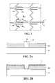
- FIG. 1is a top view of one embodiment of the micromirrors of the present invention.
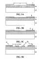
- FIGS. 2A to 2Eare cross sectional views of one method for making the micromirrors of the present invention, taken along line 2 - 2 of FIG. 1 ;
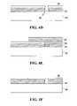
- FIGS. 3A to 3Dare cross sectional views of the same method shown in FIGS. 2A to 2E , but taken along line 3 - 3 of FIG. 1 ;
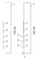
- FIGS. 4A to 4Jare cross sectional views illustrating a further method for making micromirrors for the present invention.
- FIGS. 5A to 5Gare cross sectional views illustrating yet a further method for making micromirrors in accordance with the present invention.
- FIGS. 6A to 6Care plan views of different micromirror shape and hinge combinations
- FIG. 7is a plan view of a portion of a micromirror array with multiple micromirrors the same as in FIG. 6A ;
- FIG. 8is a partially exploded isometric view of a micromirror of one embodiment of the invention.
- FIGS. 9A to 9Care cross sectional views showing actuation of a micromirror of the embodiment of FIG. 8 ;
- FIGS. 10A to 10Dare cross sectional views of a process in accordance with yet another embodiment of the invention.
- FIGS. 11A to 11Care cross sectional views showing actuation of a micromirror made in accordance with the method illustrated in FIGS. 10A to 10D ;
- FIG. 12is a plan view of multiple micromirrors in a micromirror array formed in accordance with the method of FIGS. 11A to 11C ;
- FIG. 13is a partially exploded isometric view of the micromirror of FIG. 12 ;
- FIGS. 14A to 14Cillustrate micromirrors having a flat non-deflected ‘off’ state
- FIGS. 15A to 15Cillustrate micromirrors having deflected ‘on’ and ‘off’ states of equal angles
- FIGS. 16A to 16Cillustrated micromirrors having a greater angle for the ‘on’ state than the ‘off’ state;
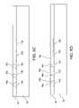
- FIGS. 17A to 17Eillustrate a package arrangement for micromirrors having an angled window
- FIG. 18is an illustration of the illumination system for the micromirror array of the present invention.
- FIGS. 19A to 19Eillustrate the relationship between angle of incident light, micromirror sides, and active area sides
- FIG. 20is an illustration of a prior art micromirror array
- FIGS. 21 and 22are illustrations of an embodiment of the invention where square micromirrors are at an angle to the active area sides;
- FIGS. 23 to 25illustrate micromirrors where “leading” and “trailing” edges of the micromirrors are not perpendicular to the incident light beam
- FIGS. 26A to 26F and 27 A to 27 Fare illustrations of micromirrors having the shapes of one or more parallelograms
- FIG. 28is an illustration of a single micromirror
- FIG. 29is an illustration of a micromirror array having part of the leading and trailing sides perpendicular to the incident light beam, and another part at a 45 degree angle to the incident light beam;
- FIGS. 30 and 31are illustrations of micromirror arrays where the micromirrors have no sides parallel or perpendicular to the incident light beam or the sides of the active area of the array;
- FIGS. 32A to 32Jare illustrations of micromirrors with corresponding hinge structures.
- FIGS. 33A to 33Care illustrations of diffraction patterns having a diffraction line passing through the acceptance cone of the collection optics ( 33 A) and avoiding the acceptance cone ( 33 B and 33 C).
- FIG. 1is a top view of one embodiment of the micromirrors of the present invention.
- posts 21 a and 21 bhold micromirror plate 24 via hinges 120 a and 120 b above a lower substrate having electrodes thereon (not shown) for causing deflection of micromirror plate 24 .
- thousands or even millions of micromirrors 24can be provided in an array for reflecting light incident thereon and projecting an image to a viewer or target/screen.
- Micromirror 24can be fabricated by many different methods.
- One methodis illustrated in FIGS. 2A to 2E (taken along cross section 2 - 2 from FIG. 1 ) where the micromirrors are fabricated on preferably a light transmissive substrate which is then bonded to a circuit substrate.
- This methodis disclosed further in U.S. Provisional Patent Application 60/229,246, to Ilkov et al., filed Aug. 30, 2000, and U.S. patent application Ser. No. 09/732,445 to Ilkov et al., filed Dec. 7, 2000. Though the method will be describe in connection with a light transmissive substrate, any other suitable substrate could be used, such as a semiconductor substrate with circuitry.
- micromirror postsmay be electrically connect to the metal 3 layer in the IC process and utilize conductive materials for at least a part of the micromirrors.
- Methods of forming micromirrors directly on a circuit substrateinstead of on a separate light transmissive substrate will be discussed in more detail further herein.
- a light transmissive substrate 13(at least prior to adding further layers thereon) such as glass (e.g., Corning 1737F or Eagle2000), quartz, PyrexTM, sapphire, etc. is provided.
- the light transmissive substratecan have an optional light blocking layer added on its lower side to help in handling the substrate during processing.
- a light blocking layercould be a TiN layer deposited by reactive sputtering to a depth of 2000 angstroms on the back side of the light transmissive substrate, which would later be removed once processing is complete.
- the substratecan be any shape or size, though one that is the shape of a standard wafer used in an integrated circuit fabrication facility is preferred.
- a sacrificial layer 14such as amorphous silicon, is deposited.
- the sacrificial layercan be another suitable material that can later be removed from under the micromechanical structural materials (e.g., SiO2, polysilicon, polyimide, novolac, etc.).
- the thickness of the sacrificial layercan be wide ranging depending upon the movable element/micromirror size and desired tilt angle, though a thickness of from 500 ⁇ to 50,000 ⁇ , preferably around 5000 ⁇ is preferred.
- the sacrificial layercould be any of a number of polymers, photoresist or other organic material (or even polysilicon, silicon nitride, silicon dioxide, etc. depending upon the materials selected to be resistant to the etchant, and the etchant selected).
- An optional adhesion promotere.g., SiO2 or SiN
- SiO2 or SiNcan be provided prior to depositing the sacrifical material.
- Hole 6 having width “d”is formed in the sacrificial layer in order to provide a contact area between the substrate 13 and later deposited micromechanical structural layers.
- the holesare formed by spinning on a photoresist and directing light through a mask to increase or decrease solubility of the resist (depending upon whether the resist is a positive or negative resist).
- Dimension “d”can be from 0.2 to 2 micrometers (preferably around 0.7 um), depending upon the ultimate size of the micromirror and the micromirror array. After developing the resist to remove the resist in the area of the holes, the holes are etched in the sacrificial amorphous silicon with a chlorine or other suitable etchant (depending upon the sacrificial material).
- the remaining photoresistis then removed, such as with an oxygen plasma.
- the hole in the sacrificial layercan be any suitable size, though preferably having a diameter of from 0.1 to 1.5 um, more preferably around 0.7+/ ⁇ 0.25 um.
- the etchingis performed down to the glass/quartz substrate or down to any intermediate layers such as adhesion promoting layers. If the light transmissive substrate is etched at all, it is preferably in an amount less than 2000 ⁇ .
- the sacrificial layer 14is a directly patternable material (e.g., a novolac or other photosensitive photoresist) then an additional layer of photoresist deposited and developed on top of the sacrificial layer 14 is not needed. In such a case, the photoresist sacrificial layer is patterned to remove material in the area of hole(s) 6 and then optionally hardened before depositing additional layers.
- a first structural layer 7is deposited by, e.g., chemical vapor deposition.
- the materialis silicon nitride or silicon oxide deposited by LPCVD (low pressure chemical vapor deposition) or PECVD (plasma enhanced chemical vapor deposition), however any suitable thin film material such as polysilicon, a metal or metal alloy, silicon carbide or an organic compound could be deposited at this point (of course the sacrificial layer and etchant should be adapted to the structural material(s) used).
- the thickness of this first layercan vary depending upon the movable element size and desired amount of stiffness of the element, however in one embodiment the layer has a thickness of from 100 to 3200 ⁇ , more preferably between 900 and 1100 ⁇ . As can be seen in FIG. 2B , layer 7 extends into the holes etched in the sacrificial layer.
- a second layer 8is deposited as can be seen in FIG. 2C .
- the materialcan be the same (e.g., silicon nitride) as the first layer or different (silicon oxide, silicon carbide, polysilicon, etc.) and can be deposited by chemical vapor deposition as for the first layer.
- the thickness of the second layercan be greater or less than the first, depending upon the desired stiffness for the movable element, the desired flexibility of the hinge, the material used, etc.
- the second layerhas a thickness of from 50 ⁇ to 2100 ⁇ , and preferably around 900 ⁇ .
- the first layeris deposited by PECVD and the second layer by LPCVD.
- both the first and second layersare deposited in the areas defining the movable (micromirror) element and the posts.
- the first and second layersare deposited in the areas defining the movable (micromirror) element and the posts.
- a single layercould be provided in place of the two layers 7 , 8 for all areas of the microstructure, though this could involve a tradeoff in plate stiffness and hinge flexibility.
- the area forming the hingecould be partially etched to lower the thickness in this area and increase the flexibility of the resulting hinge.
- a reflective layer 9is deposited.
- the reflective materialcan be gold, silver, titanium, aluminum or other metal, or an alloy of more than one metal, though it is preferably aluminum deposited by PVD.
- the thickness of the metal layercan be from 50 to 2000 ⁇ , preferably around 500 ⁇ .
- An optional metal passivation layer(not shown) can be added, e.g., a 10 to 1100 ⁇ silicon oxide layer deposited by PECVD on top of layer 9 .
- Other metal deposition techniquescan be used for depositing metal layer 9 , such as chemical fluid deposition and electroplating. After depositing layer 9 , photoresist is spun on and patterned, followed by etching of the metal layer with a suitable metal etchant.
- a chlorine (or bromine) chemistrycan be used (e.g., a plasma/RIE etch with Cl 2 and/or BCl 3 (or Cl2, CCl4, Br2, CBr 4 , etc.) with an optional preferably inert diluent such as Ar and/or He).
- a plasma/RIE etchwith Cl 2 and/or BCl 3 (or Cl2, CCl4, Br2, CBr 4 , etc.) with an optional preferably inert diluent such as Ar and/or He).
- the reflective layerneed not be deposited last, but rather could be deposited directly upon the sacrificial layer 14 , between other layers defining the micromirror element, or as the only layer defining the micromirror element.
- the first and second layers 7 , 8can be etched subsequent to the reflective layer with known etchants or combinations of etchants (depending upon the material used and level of isotropy desired).
- the first and second layerscan be etched with a chlorine chemistry or a fluorine (or other halide) chemistry (e.g., a plasma/RIE etch with F 2 , CF 4 , CHF 3 , C 3 F 8 , CH 2 F 2 , C 2 F 6 , SF 6 , etc.
- Gaps 20 a and 20 b having a width “e” shown in FIG. 2Eare for separating the post 21 from the micromirror body 22 .
- FIGS. 3A to 3Dillustrate the same process taken along a different cross section (cross section 3 - 3 in FIG. 1 ) and show the light transmissive substrate 13 , on which is deposited a sacrificial layer 14 .
- On sacrificial layer 14is deposited structural layer 7 .
- a part of layer 7is removed prior to adding layers 8 and 9 . This portion removed is in the area where the hinge is to be formed, and allows for increased flexibility in the hinge area.
- This “thinning” of the hinge area in this wayis set forth in U.S. Provisional Patent Application 60/178,902 to True et al., filed Jan. 28, 2000, and in U.S. patent application Ser. No.
- hinges 23After removing portions of layer 7 , layers 8 and 9 are added, followed by patterning of layers 7 , 8 and 9 as set forth above. As can be seen in FIG. 3D , hinges 23 have width “a” that can be from 0.1 to 10 um, preferably around 0.7 um. The hinges 23 are separated from each other by a gap “b” and from adjacent micromirror plates by gaps “c” that also can be from 0.1 to 10 um, preferably around 0.7 um.
- a glass wafersuch as a Corning 1737F, Eagle 2000, quartz or sapphire wafer
- an opaque coatingsuch as a Cr, Ti, Al, TaN, polysilicon or TiN or other opaque coating at a thickness of 2000 angstroms (or more depending upon the material) on the backside of the wafer, in order to make the transparent substrate temporarily opaque for handling.
- an optional adhesion layeris deposited (e.g., a material with dangling silicon bond such as SiNx- or SiOx, or a conductive material such as vitreous carbon or indium tin oxide)
- the sacrificial materialcould be deposited by LPCVD at 560 C, along the lines set forth in U.S. Pat. No. 5,835,256 to Huibers et al., incorporated herein by reference.
- the sacrificial materialcould be deposited by sputtering, or could be a non-silicon containing material such as an organic material (to be later removed by, e.g., plasma oxygen ash).
- the a-Siis patterned (photoresist and etched by a chlorine chemistry, e.g., Cl2, BCl3 and N2), so as to form holes for attachment of the micromirror to the glass substrate.
- the materialcould be an aluminum alloy (Al—Si (1%), Al—Cu (0.5%) or AlSiCu or AlTi), as well as an implanted or target doped aluminum.
- the backside TiNis etched in a BCl3/Cl2/CF4 chemistry in plasma (or other metal etchant from CRC Handbook of Metal Etchants)—or polished or ground off using CMP, or removed with acid vapor such as HF—followed by a second ACT clean (acetone+DI wafer solution) and a second spin dry.
- the etchis performed by providing the die in a chamber of N2 at around 400 Torr.
- a second area/chamberhas therein 3.5 Torr XeF2 and 38.5 Torr He.
- a barrier between the two areas/chambersis removed, resulting in the combined XeF2, He and N2 etching mixture.
- the transparent wafere.g., Corning 1737F
- TiNtitanium-nitride
- the a-Siis patterned (photoresist and etched by a chlorine chemistry, e.g., Cl2, BCl3 and N2-50 W), so as to form holes for attachment of the micromirror to the glass substrate.
- a second layer of silicon nitrideis deposited by PECVD (same conditions as first layer) at a thickness of 900 Angstroms.
- Alis sputtered (150 C) onto the second silicon nitride layer at a thickness of 500 Angstroms.
- the aluminumis patterned in the P5000 with a chlorine chemistry (BCl3, Cl2, Ar).
- the SiN layersare etched (CHF3, CF4), followed by ashing in a barrel asher (O2, CH3OH at 250 C).
- the remaining structuresare cleaned with EKC Technology's EKS265 photoresist residue remover.
- the backside TiNis etched in a SF6/Ar plasma, followed by a second clean and a second spin dry.
- the waferis singulated and each die then is placed in a Drytek parallel plate RF plasma reactor.
- 100 sccm of CF4 and 30 sccm of O2flow to the plasma chamber, which is operated at about 200 mtorr for 80 seconds.
- the dieis etched for 300 seconds at 143 Torr etch pressure (combined XeF2, He and N2).
- the etchis performed by providing the die in a chamber of N2 at around 400 Torr.
- a second area/chamberhas therein 5.5 Torr XeF2 and 20 Torr He.
- each micromirrorcan be formed essentially in the same plane as the micromirror element (layers 7 , 8 and 9 for the micromirror body vs. layers 8 and 9 for the micromirror hinge in FIG. 3D ) as set forth above, they can also be formed separated from and parallel to the micromirror element in a different plane and as part of a separate processing step (after deposition of a second sacrificial material).
- This superimposed type of hingeis disclosed in FIGS. 8 and 9 of the previously-mentioned U.S. Pat. No. 6,046,840, and in more detail in U.S. patent application Ser. No. 09/631,536 to Huibers et al., filed Aug.
- a second substratecontains a large array of electrodes on a top metal layer (e.g., metal 3 ) of the substrate (e.g., a silicon wafer). As can be seen in FIG.
- the micromirrors 44are kept spaced apart from the electrodes on substrate 60 by spacers 41 (e.g., photoresist spacers adjacent every micromirror and/or spacers deposited within epoxy when bonding substrate 40 to substrate 60 .
- One or more electrodes on the circuit substrateelectrostatically control a pixel (one micromirror on the upper optically transmissive substrate) of the microdisplay.
- the voltage on each electrode on the surface of the backplanedetermines whether its corresponding microdisplay pixel is optically ‘on’ or ‘off,’ forming a visible image on the microdisplay.
- the release of the micromirrors of the present inventioncan be a single or multi-step process, with the type of process depending upon the type of sacrificial material used.
- the first etchis performed that has relatively low selectivity (e.g., less than 200:1, preferably less than 100:1 and more preferably less than 10:1), and a second etch follows that has higher selectivity (e.g., greater than 100:1, preferably greater than 200:1 and more preferably greater than 1000:1).
- selectivitye.g., less than 200:1, preferably less than 100:1 and more preferably less than 10:1
- a second etchfollows that has higher selectivity (e.g., greater than 100:1, preferably greater than 200:1 and more preferably greater than 1000:1).
- Such a dual etchingis set forth further in U.S. Patent Application 60/293,092 to Patel et al., filed May 22, 2001, incorporated herein by reference.
- other release methodscould be used, depending upon the
- oxygen plasma ashing or a supercritical fluid releasecould be used.
- Plasmas containing pure oxygencan produce species that attack organic materials to form H2O, CO and CO2 as products and do not etch SiO2, Al or Si.
- an etchantsuch as an isotropic dry etchant (CHF3+O2, NF3 or SF6) could be used.
- the sacrificial materialis silicon nitride
- fluorine atomscould be used to isotropically etch the silicon nitride (e.g., CF4/O2, CHF3/O2, CH2F2 or CH3F plasmas).
- fluorine atoms in the form of XeF2, BrF3 or BrCl3could be used.
- the sacrificial layeris aluminum, then a chlorine chemistry (BCL3, CCl4, SiCl4) could be used.
- any etchant (and sacrificial material)would be selected at least in part based upon the amount of undercut etching needed.
- a substrate 30(this can be any suitable substrate, such as a glass/quartz substrate or a semiconductor circuit substrate) that has deposited thereon a sacrificial material 31 .
- Any suitable sacrificial materialcan be used, preferably one that has a large etching selectivity ratio between the material being etched and the sacrificial material.
- One possible sacrificial materialis an organic sacrificial material, such as photoresist, or other organic materials such as set forth in U.S. Patent Application 60/298,529 filed Jun. 15, 2001 to Reid et al.
- a photoresist layer 32is added and developed to form one or more apertures ( FIG. 4B ). Then, as can be seen in FIG. 4C , apertures 34 are etched into the sacrificial material 31 and the photoresist 32 is removed. As can be seen in FIG. 4D , a (preferably conductive) layer 35 is deposited that will ultimately form at least the flexible portions for the MEMS device (in this example a micromirror structure).
- Layer 35can also form the posts 36 for attaching the micromirror to the substrate, or even all or part of the micromirror body.
- the conductive layer 35 in a preferred embodiment of the inventioncomprises a metal-Si,Al,B-nitride, preferably the metal is a transition metal, in particular a late transition metal.
- Layer 35could also be a plurality of (preferably conductive) layers, or one conductive layer among many other types of layers (structural dielectric layers, reflective layers, anti-stiction layers, etc.). Layer 35 need not be conductive, and depending upon the exact method, target material and atmosphere used in the deposition process, layer 35 could also be insulating.
- FIG. 4Eshows the addition of photoresist 37 (patterned) followed by etching of a portion of the nitride layer(s) 35 and removal of the photoresist ( FIG. 4F ).
- micromirror structural material layer 38is deposited.
- the materialcan be conductive or insulating, and can be a plurality of layers. If the material is a single layer, it is preferably reflective (e.g., an aluminum or gold layer or metal alloy layer).
- photoresist 39is added and developed followed by ( FIG. 41 ) etching/removing portions of the layer 38 (such as in the area of the parts that will flex in operation).
- the sacrificial layeris removed to release the MEMS device so as to be free standing on the substrate.
- circuitrythat is formed on or in substrate 30 (if the substrate is a circuit substrate) or a light blocking layer on substrate 30 for improving automated handling of the substrate (if the substrate is a light transmissive substrate such as glass, quartz, sapphire, etc.).
- a free standing MEMS structureis created where layer 35 forms a flexible portion of the MEMS device, whereas layer 38 forms the structure that moves due to the flexible nature of layer 35 .
- Layer 38forms both the movable portion as well as the post or wall that holds the MEMS structure on the substrate 30 .
- the movable elementcan be formed as a laminate of layers 38 and 35 (as well as additional layers if desired), or solely from layer 38 , or even solely from layer 35 .
- the make-up of the movable and flexible elementsdepend upon the ultimate stiffness or flexibility desired, the ultimate conductivity desired, the MEMS device being formed, etc.
- the micromirrors formed in accordance with FIGS. 1 to 4are preferably formed on a light transmissive substrate and have a non-deflected ‘off’ state and a deflected ‘on’ state.
- the micromirrorscan be formed on the same substrate as micromirror actuation circuitry and electrodes.
- both the ‘on’ and ‘off’ states of the micromirrorcan be a position other than a flat non-deflected state.
- the micromirrorsare formed on the same substrate as electrodes and circuitry for moving the micromirrors.
- a semiconductor substrate with circuitry and electrodes formed thereon (or therein)can be the starting substrate for making micromirrors in accordance with the present invention.
- a semiconductor substrate 10 with circuitry for controlling the micromirrorhas a patterned metal layer formed into discrete areas 12 a to 12 e thereon—typically aluminum (e.g., the final metal layer in a semiconductor process).
- a sacrificial layer 14is deposited thereon, as can be seen in FIG. 5B .
- the sacrificial materialcan be selected from many materials depending upon the adjacent structures and etchant desired.
- the sacrificial materialis a novolac photoresist.
- FIG. 5Aa semiconductor substrate 10 with circuitry for controlling the micromirror
- apertures 15 a and 15 bare formed in the sacrificial material by standard patterning methods for a novolac photoresist, so as to form apertures 15 a to 15 c connecting to metal areas 12 a to 12 c .
- plugs or other connections 16 a to 16 care formed in accordance with standard plug forming methods.
- Tungsten (W)could be deposited by CVD by a) silicon reduction: 2WF6+3Si ⁇ 2W+3SiF4 (This reaction is normally produced by allowing the WF6 gas to react with regions of exposed solid silicon on a wafer surface at a temperature of about 300 C), b) hydrogen reduction: WF6+3H2 W+6HF (This process is carried out at reduced pressures, usually at temperatures below 450 C), or c) silane reduction: 2WF6+3SiH4 ⁇ 2W+3SiF4+6H2 (This reaction (LPCVD at around 300 C) is widely used to produce a W nucleation layer for the hydrogen reaction).
- CMPchemical mechanical polishing
- a linerin order to avoid peeling (e.g., for a tungsten plug, a TiN, TiW or TiWN liner could be deposited to surround the tungsten in the hole in the sacrificial material and later after release of the sacrificial layer).
- a conductive layeris deposited and patterned so as to result in discrete metal areas 18 a to 18 c , each electrically connected to underlying metal areas 12 a to 12 c , respectively, via plugs 16 a t 0 16 c , respectively.
- the conductive layercan be any suitable material (aluminum, alloys of aluminum, alloys of other metals, conductive ceramic compounds, etc.) that is deposited by suitable methods such as physical vapor deposition or electroplating. The material should preferably have both conductive properties as well as a proper combination of hardness, elasticity, etc. (as will be seen, area 18 c will act as a hinge for the micromirror being formed).
- this conductive layeris either an aluminum alloy or a conductive binary or ternary (or higher) compound such as those disclosed in U.S. Patent Application 60/228,007 to Reid filed Aug. 23, 2000 and U.S. Patent Application 60/300,533 to Reid filed Jun. 22, 2001, both incorporated herein by reference, deposited by reactive sputtering.
- the appropriate etching chemistryis used to pattern the conductive layer (e.g., a chlorine chemistry for aluminum) so as to form discrete conductive areas 18 a to 18 c.
- a second layer of sacrificial layer 20is deposited that could be the same or different from the sacrificial material of layer 14 (preferably the material is the same so that both layers can be removed simultaneously). Then, layer 20 is patterned so as to form aperture 20 a down to area 18 c . As with forming apertures in sacrificial layer 14 , this can be done with an additional layer of photoresist or layer 20 can be directly patterned if the material is a photoresist or other directly patternable material. As can be seen in FIG.
- a plug or connection 22is formed by depositing a preferably electrically conductive material on sacrificial layer 20 , followed by chemical mechanical polishing, leaving plug 22 connected to discrete area (“hinge”) 18 c .
- micromirror body 24is formed by depositing a (preferably conductive) layer followed by patterning into the desired shape of the micromirror.
- Many micromirror shapesare possible, such as that illustrated in FIG. 6A , and as will be discussed in further detail herein.
- the micromirror shape in accordance with this example of the inventioncan have any shape, including square or diamond as shown in FIGS. 6B and 6C .
- Dotted line 62 in FIG. 6Cis the axis or rotation of the micromirror.
- each layer(whether structural or sacrificial) could be provided as a laminate e.g., one layer of the laminate having improved mechanical performance and another layer having improved conductivity.
- the structural materialsare conductive, it is possible to make micromirror element 24 (or a layer within a laminate 24 ) conductive, as well as actuation electrodes 12 d and 18 b (and layers/materials connecting electrodes 12 d and 18 b to the semiconductor substrate).
- the materials disclosed aboveneed not contain any metal, but could, for example be silicon (e.g., polycrystalline silicon) or a compound of silicon (e.g., Si3N4, SiC, SiO2, etc.). If Si3N4 is used as a structural material and amorphous silicon is used as the sacrificial material, xenon difluoride could be utilized as a gas phase etchant in order to remove the sacrificial amorphous silicon. If desired, the silicon or silicon compound (or other compound) used as a structural material could be annealed before and/or after removing the sacrificial layer to improve the stress characteristics of the structural layer(s).
- FIG. 8is an exploded view of the micromirror formed in accordance with FIGS. 5A to 5G .
- FIG. 9Ais an illustration of the micromirror after removal of the two sacrificial layers, showing micromirror 24 connected to substrate 10 via post 22 , hinge 18 c , post 16 c and metal areas 12 c .
- the micromirror as shown in FIG. 9Ais not moved or deflected, as no voltages are applied to any underlying electrodes (discrete metal areas formed in the above-described process) e.g., electrodes 18 b or 12 d .
- This non-deflected positionis not the ‘off’ position for the micromirror, which for projection systems is generally the furthest angle away from the ‘on’ position (in order to achieve the best contrast ratio for the projected image).
- the ‘on’ state of the micromirrorthat is, the position of the micromirror that deflects light into the acceptance cone of the collection optics, is illustrated in FIG. 9B .
- a voltage V Ais applied to electrode 12 d in order to electrostatically pull down micromirror plate 24 until the edge of plate 24 impacts electrode 12 e .
- Both micromirror plate 24 and electrode 12 eare at the same potential, in this example at a voltage of V 0 . As illustrated in FIG.
- micromirror plate 24when a voltage V B is applied to electrode 18 b , micromirror plate 24 deflects in an opposite direction, with its movement being stopped by electrode 18 a . Both electrode 18 a and micromirror plate 24 are at the same potential (in this example a V 0 voltage). Depending upon the size of electrode 18 b vs. electrode 12 d , and the distance between these electrodes and the micromirror plate 24 , the voltages applied to electrodes 18 b and 12 d need not be the same.
- This deflected position illustrated in FIG. 9Cis the ‘off’ position, and deflects light furthest away from the collection optics.
- the off positionforms a lower angle (with the substrate) than the on position.
- a sign of the anglewill be used (positive or negative relative to the substrate or non-deflected position).
- the signis arbitrary, but signifies that the micromirrors rotate in one direction to an ‘on’ position and in an opposite direction to an ‘off’ position. The benefits of such asymmetry will be discussed in further detail below.
- the on positionis from 0 to +30 degrees and the off position is from 0 to ⁇ 30, with movement to the on position being greater than movement to the off position.
- the on positioncould be from +10 to +30 degrees (or +12 to +20 degrees or +10 to +15 degrees) and the off position could be greater than 0 and between 0 and ⁇ 30 degrees (or within a smaller range of between 0 and ⁇ 10 or ⁇ 12, or from ⁇ 1 to ⁇ 12, or ⁇ 1 to ⁇ 10 or ⁇ 11 degrees, or ⁇ 2 to ⁇ 7 degrees).
- the micromirrorsare capable of rotating at least +12 degrees to the on position and between ⁇ 4 and ⁇ 10 degrees to the off position.
- the on and off positionsare at angles greater than 3 degrees but less than 30 degrees relative to the substrate, preferably the on position is greater than +10 degrees, and that the mirrors rotate 1 degree (or more) further in the on direction than in the opposite off direction.
- FIGS. 10A to 10Dillustrate a further method and micromirror structure. Variability in materials, layers, sacrificial etching, depositing of structural layers, etc. are as above with respect to the previously described processes.
- the substrate 40could be either a light transmissive substrate (to later be joined to a second substrate with circuitry and electrodes) or a semiconductor substrate already having circuitry and electrodes thereon.
- the circuitry and electrodesare formed on a separate substrate.
- a sacrificial layer 42is deposited and patterned so as to form aperture 43 .
- plug 46is formed (preferably as in the process of FIG. 5 A to 5 G—deposit a metal, metal alloy or other conductive layer and planarize (e.g., by CMP) to form the plug).
- a hinge 50is formed by depositing an electrically conductive material (having suitable amorphousness, elasticity, hardness, strength, etc.).
- the hingeis an early transition metal silicon nitride such as Ta—Si—N, a late transition metal silicon nitride such as Co—Si—N or a metal or metal-ceramic alloy such as a titanium aluminum alloy, or a titanium aluminum oxide alloy.
- a photoresistis deposited and patterned so as to allow for etching/removal of all areas except for the hinge areas 50 .
- micromirror plate 44is formed by first protecting the hinges with photoresist and then depositing and patterning a hinge structure layer so as to form micromirror plate 44 partially overlapping and therefore connecting with hinge 50 .
- an array of thousands or millions of such micromirrorsis formed at the same time in an array.
- the substrate with micromirrorsis attached to a substrate with actuation circuitry and electrodes.
- the second substrate 60 with electrodes 72 and 74 for deflecting the micromirror, and a landing pad or electrode 70is illustrated in FIG. 11A .
- the micromirroris in a non-deflected position in FIG. 11A .
- micromirror 44When a voltage V A is applied to electrode 72 , micromirror 44 is deflected until it impacts electrode 70 ( FIG. 11B ). This is the ‘on’ position of the micromirror that allows light to enter into the collection optics of the system. It is possible to design the gap between the substrates so that the ends of micromirror plate 44 impact electrode 70 and substrate 40 at the same time.
- V BWhen a voltage V B is applied to electrode 74 , micromirror plate 44 deflects in the opposite direction until the end of the micromirror impacts substrate 40 . This is the ‘off’ position of the micromirror ( FIG. 11C ).
- FIG. 12An array of such micromirrors is illustrated in FIG. 12 , and an exploded view of a micromirror made in accordance with the process of FIGS. 10A to 10D is shown in FIG. 13 .
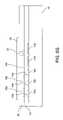
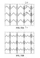
- FIG. 14Ais a cross sectional view of multiple micromirrors within an array where micromirrors in their ‘off’ state are not deflected (group 100 ) whereas micromirrors in their ‘on’ state (group 102 ) are moved from the flat state so as to project light where the light can be viewed (directly, on a target within a unitary device, across a room onto a screen, etc.).
- Such a micromirror array arrangementis better illustrated in FIGS. 14B and 14C . As can be seen in FIG.
- FIG. 14Bin the micromirrors' ‘on’ state, an incoming cone of light 50 is reflected off of the micromirrors (all micromirrors are ‘on’ in this figure) and light is projected away as a cone of light 52 into output aperture 60 , and in most cases will proceed to an imaging system (e.g., a projection lens or lenses).
- Cone 54represents specular reflection from the transparent cover.
- FIG. 14Cis an illustration of the micromirrors in their ‘off’ state, where cone 52 represents light reflected from the micromirrors in this ‘off’ state. The incident and reflected cones of light will narrow onto the entire array, though in these figures, for ease of illustration, the cones of light are shown as tapering onto an individual micromirror.
- FIGS. 14B and 14Chas the benefit that when the micromirrors are in their ‘off’ (non-deflected) state, little light is able to travel through the gaps between the micromirrors and cause undesirable “gap scatter”. However, as shown in FIG. 14C , diffracted light is caused by the repeating pattern of the micromirrors (light 61 a and 61 b that extends beyond the cone of reflected ‘off’ light 52 ). This undesirable light is caused by scattering or diffraction from the edges of the micromirrors (“edge scatter”).
- diffraction lightsuch as light 61 a that extends beyond the cone of reflected ‘off’ light can enter the output aperture 60 (e.g., collection optics) and undesirably decrease contrast ratio.
- the ‘off’ state light and ‘on’ state lightcan be separated further from each other by deflecting micromirrors for both the ‘on’ and ‘off’ states.
- deflecting micromirrorsfor both the ‘on’ and ‘off’ states.
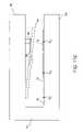
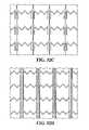
- FIG. 15Aif the micromirror is deflected in its ‘off’ state as illustrated in this figure, some light will be properly reflected off of the micromirrors far away from the ‘on’ state direction (e.g., collection optics) as shown as ray 116 .
- the ‘off’ state along with diffraction 61 a caused by micromirror periodicityis moved further away from the ‘on’ angle so as to result in improved contrast ratio due to diffraction/edge scatter (though decreased contrast ratio due to gap scatter, as mentioned above).
- An improved micromirror arraywould maximize the distance between the ‘off’ light cone and the ‘on’ light cone (minimize edge scatter into the acceptance cone), yet minimize gaps between adjacent micromirrors (minimize gap scatter).
- One solution that has been triedhas been to provide a micromirror array with micromirrors that deflect in opposite directions for the ‘on’ and ‘off’ states as in FIGS. 15A to 15C , and provide a light absorbing layer under the micromirrors so as to decrease gap scatter.
- micromirrorsare provided that are deflected in both their ‘on’ and ‘off’ states, yet at different deflection angles.
- micromirrors 100are deflected in an ‘off’ state that is at a deflection angle less than micromirrors 102 in their ‘on’ state (deflected in an opposite direction from the flat or nondeflected position).
- the ‘on’ stateis unchanged (incoming light 50 projected as outgoing light 52 into output aperture 60 ), with some specular reflection 54 .
- micromirrorsare in their ‘off’ state in a sufficiently deflected position such that edge scattering light 61 a that passes into output aperture 60 is minimized, yet deflected only so much as to keep such edge scattering light out of the acceptance cone so as to minimize gap scattering light from under the micromirrors due to a large off state deflection angle.
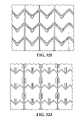
- An additional feature of the inventionis in the packaging of the device.
- reflection off of the light transmissive substratecan result in specular reflection.
- incoming light cone 50reflects off of micromirrors in their on position, illustrated as reflected cone 52 .
- Specular light reflected from a surface of the light transmissive substrate 32is illustrated as light cone 54 . It is desirable in making a projection system, to increase the distended angle of the cone so as to increase etendue and projection system efficiency.
- FIG. 17Aincoming light cone 50 reflects off of micromirrors in their on position, illustrated as reflected cone 52 .
- Specular light reflected from a surface of the light transmissive substrate 32is illustrated as light cone 54 . It is desirable in making a projection system, to increase the distended angle of the cone so as to increase etendue and projection system efficiency.
- light transmissive substrate 32is placed at an angle relative to substrate 30 .
- substrate 30is the substrate upon which the micromirrors (or other optical MEMS elements) are formed
- substrate 32is a light transmissive window in a package for the optical MEMS device.
- the angle of the windowis greater than ⁇ 1 degree (the minus sign in keeping with the directions of the angles or the micromirrors).
- the windowis at an angle of from ⁇ 2 to ⁇ 15 degrees, or in the range of from ⁇ 3 to ⁇ 10 degrees.
- the windowis at an angle relative to the micromirror substrate that is preferably in the same “direction” as the off position of the micromirrors (relative to the micromirror substrate and/or package bottom).
- the micromirrorswhen the micromirrors are in the ‘on’ state, there is a gap between the light reflected as light from ‘on’ micromirrors (light reflectance cone 52 ) and specular reflection light (light cone 54 ). This “gap” is due to specular reflection cone 54 being reflected at a greater distance due to the angled light transparent substrate. This arrangement allows, as can be seen in FIG.
- FIGS. 17B and 17Cfor increasing the distended angle of the incident light cone (and the corresponding reflectance light cones) from the ‘on’ micromirrors (cone 52 ) and the light transparent substrate (cone 54 ).
- the reflectance point of the light conesis midway between the micromirror and the light transmissive substrate, though in reality light cone 52 reflects from the micromirror(s) and specular reflection cone 54 reflects from the substrate 32 .
- a light valve such as illustrated in FIGS. 17B and 17Cis capable of modulating a larger etendue light beam and can pass through more light from a light source and is thus more efficient).
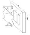
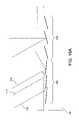
- FIGS. 17D and 17EA packaged device is illustrated in FIGS. 17D and 17E .
- incoming light 40(this view is reversed from previous views) is incident on the array and reflected therefrom.
- an angled light transmissive substrate 32(with mask areas 34 a and 34 b ) not only allows for increased light cone distended angles as noted above, but in addition a gap between the mask of window 32 and the micromirror array is minimized, thus reducing light scattering and temperature build-up in the package.
- the angle of the light transmissive windowis from 1 to 15 degrees relative to the substrate, preferably from 2 to 15 degrees, or even from 3 to 10 degrees. As can be seen in FIGS.
- bond wires 37 at one end of the substrate in the packageare disposed where the angled window is at a greater distance than at an opposite end of the substrate.
- the angled windowallows for the presence of bond wires, yet allows for a minimized distance between the light transmissive window and the micromirror substrate at an end of the substrate where there are no bond wires. Note that light is incident on the micromirror array from a side of the package corresponding to the position of the bond wires and elevated side of the angled window.
- package adhesivese.g. epoxy adhesives, molecular scavengers or other getters, a source of stiction reducing agent (e.g. chlorosilanes, perfluorinated n-alkanoic acids, hexamethyldisilazane, etc.).
- a source of stiction reducing agente.g. chlorosilanes, perfluorinated n-alkanoic acids, hexamethyldisilazane, etc.
- the micromirrors of the present inventionare for a projection display, there should be a suitable light source that illuminates the array and projects the image via collection optics to a target.
- the arrangement of light source and incident light beam to the array, and to each micromirror, which allows for the improved contrast ratio while minimizing projection system footprint, in the present invention,can be seen in FIGS. 18 and 19 a to 19 c .
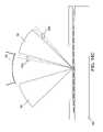
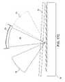
- a light source 114directs a beam of light 116 at a 90 degree angle to the leading side 93 of the active area of the array (the active area of the array illustrated as rectangle 94 in the figure).
- the active area 94would typically have from 64,000 to about 2,000,000 pixels in a usually rectangular array such as illustrated in FIG.
- the active area 94reflects light (via ‘on’ state micromirrors) through collection optics 115 to a target to form a corresponding rectangular image on the target (e.g., wall or screen).
- the arraycould be a shape other than rectangular and would result in a corresponding shape on the target (unless passed through a mask).
- Light from light source 114reflects off of particular micromirrors (those in the ‘on’ state) in the array, and passes through optics 115 (simplified as two lenses for clarity).
- Micromirrors in their ‘off’ statein a non-deflected “rest” state), direct light to area 99 in FIG. 18 .
- a projection systemthat could have additional components such as TIR prisms, additional focusing or magnification lenses, a color wheel for providing a color image, a light pipe, etc. as are known in the art.
- additional componentssuch as TIR prisms, additional focusing or magnification lenses, a color wheel for providing a color image, a light pipe, etc.
- a color wheel and different collection opticscould be used.
- a targetmay not be a screen or photoresist, but could be a viewer's retina as for a direct view display.
- all ‘on’ micromirrors in the arraydirect light together to a single collection optic, which can be one lens or a group of lenses for directing/focusing/projecting the light to a target.
- the pixels on the screen image(each pixel on the viewed or projected image corresponding to a micromirror element in the array) have sides that are not parallel to at least two of the four sides defining the rectangular screen image.
- the incident light beamdoes not impinge perpendicularly on any sides of the micromirror element.
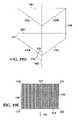
- FIG. 19Ais a perspective view of light hitting a single micromirror element
- FIG. 19Bis a top view
- FIG. 19Cis a side view.
- the incident light beammay be from 10 to 50 degrees (e.g., 20 degrees) from normal (to the micromirror/array plane). See angle 133 in FIG. 19C .
- the micromirror sidesshould be disposed at an angle ( 131 ) less than 80 degrees or preferably 55 degree or less in relation to the incident light beam axis projection on the micromirror plane ( 102 ), more preferably 45 degrees or less, and most preferably 40 degrees or less.
- angle 132should be 100 degrees or more, preferably 125 degrees or more, more preferably 135 degrees or more, and most preferably 140 degrees or more.
- the switching (i.e., rotational) axis of the micromirroris labeled as dotted line 103 in FIG. 19D .
- This switching axiscould be in other places along the micromirror, e.g., line 106 , depending upon the type of hinges utilized.
- the switching axise.g., 103 or 106
- FIG. 19Eis a top view—however an array of micromirrors are illustrated in FIG. 19E along with an incident light beam 102 onto the 2-D array of micromirrors. Note that each micromirror in FIG.
- FIG. 19Ehas the shape of the micromirror illustrated in FIGS. 19A-D .
- the overall shape of the micromirror arrayis a rectangle.
- Each of the four sides of the array, 117 - 120is defined by drawing a line between the most remote pixels in the last row and column of the active area ( 121 - 124 ) (e.g., side 119 being defined by a line intersecting corner pixels 123 and 122 ). Though it can be seen in FIG.
- each of the “leading” (closest to the light source) and “trailing” (furthest from the light source) active area sides 119 , 117is “jagged” due to the shape of the micromirrors in the active area, it should be remembered that there could be up to about 3,000,000 micromirrors or more in an area of from 1 cm 2 to 1 in 2 . Therefore, unless under extreme magnification, the active area will be essentially rectangular, with active area sides 118 and 120 (or 117 and 119 ) parallel to micromirror sides 107 and 108 in FIG. 19D (the micromirror in FIG. 19D being one of the micromirror elements within the active area of FIG.
- FIG. 19Ecould also be seen as the projected image comprising a large number of projected pixels (each projected pixel having the shape illustrated in FIG. 19D ).
- the projected image sides 118 and 120are parallel to projected pixel sides 107 and 108 , and projected image sides 117 and 119 (or 118 and 120 ) being non-perpendicular to projected pixel sides 125 a - d.
- each micromirror sideis either perpendicular or parallel to the sides of the active area.
- the micromirror sidesare neither parallel nor perpendicular to the active area sides.
- some of the sidesare neither parallel nor perpendicular to active area sides, and some sides can be parallel to active area sides (as long as also parallel to the direction of a line superimposed on the plane of the micromirror from the incident light beam).
- FIG. 22achieves high contrast ratio.
- the micromirror arrangements such as illustrated in FIGS. 23-29simplify the addressing scheme. More particularly, FIGS. 23-29 have the advantage of not positioning the pixels on a lattice aligned at an angle to the X and Y axes of the array.
- FIGS. 23-29avoids non-trivial video preprocessing to render an acceptable image on a display. Also the arrangement of FIGS. 23-29 avoids a more complicated layout of the display backplane (in relation to FIGS. 13 and 14 , which could require twice as many row or column wires to the pixel controller cells).
- Horizontal line 80 in FIG. 22connects the top row of micromirror elements, and vertical lines 81 A-D extend from each of these top row micromirrors (these horizontal and vertical lines corresponding to addressing rows and columns in the array). As can be seen in FIG. 22 , only every other micromirror is connected in this way. Thus, in order for all micromirrors to be addressed, twice as many rows and columns are needed, thus resulting in added complexity in addressing the array.
- FIG. 22also shows support posts 83 at the corners of the micromirrors that support posts connect to hinges (not shown) below each micromirror element (the “superimposed hinges” discussed hereinabove) and to an optically transmissive substrate (not shown) above the micromirror elements.
- an array 92is provided.
- a light beam 90is directed at the array such that no micromirror sides are perpendicular to the incident light beam.
- the leading sides of the micromirrorsare at an angle of about 135 degrees to the incident light beam ( 90 ). It is preferred that this angle be greater than 100 degrees, preferably greater than 130 degrees.
- the contrast ratiois further improved if the angle between the incident light beam and the leading side is 135 degrees or more, and can even be 140 degrees or more.
- the micromirror elements' orientationdoes not result in addressing issues as discussed above with respect to FIG. 22 .
- Posts 95connect to hinges (not shown) below each micromirror element in FIG. 23 .
- the hingesextend perpendicularly to the direction of the incident light beam (and parallel to the leading and trailing sides 91 B and 91 D of the active areas).
- the hingesallow for an axis of rotation of the micromirrors that is perpendicular to the incident light beam.
- FIG. 24is an illustration of micromirrors similar to that shown in FIG. 23 .
- the micromirror elementsare “reversed” and have their “concave” portion as their leading side. Even though the micromirrors in FIG. 24 are reversed from that shown in FIG. 23 , there are still no sides of the micromirrors that are perpendicular to the incident light beam.
- FIG. 24illustrates a hinge 101 disposed in the same plane as the micromirror element to which the hinge is attached. Both types of hinges are disclosed in the '840 patent mentioned above.
- FIG. 24illustrates a hinge 101 disposed in the same plane as the micromirror element to which the hinge is attached. Both types of hinges are disclosed in the '840 patent mentioned above.
- each micromirror 25likewise illustrates a hinge 110 in the same plane as the micromirror array, and shows both “convex” portions 112 (“protrusions”) and “concave” portions 113 (“cut-outs”) on the leading side of each micromirror. Due to the concave or cut-out portion of each micromirror, each micromirror is in a shape of a concave polygon. Though the micromirrors can be convex polygons (if no sides of the convex polygonal micromirrors are parallel to the leading side of the active area), it is preferred that the micromirrors have a concave polygon shape.
- Convex polygonsare known as polygons where no line containing a side can go through the interior of the polygon.
- a polygonis concave if and only if it is not a convex polygon.
- the concave polygon shapecan be in the form of a series of (non-rectangular) parallelograms, or with at least one concave and a matching at least one convex portion (for fitting within the concave portion of the adjacent micromirror), though any concave polygon shape is possible.
- the micromirror shapecould also be that of a single (non-rectangular) parallelogram.
- the matching one or more protrusions and one or more cut-outsneed not be composed of straight lines (nor any of the micromirror sides for that matter), but instead could be curved.
- the protrusion(s) and cut-out(s)are semicircular, though the illustrated angular protrusions and cut-outs are preferred.
- FIGS. 26A to 26Fillustrate further embodiments of the invention.
- eachis the same in that none has any sides perpendicular to the incident light beam.
- the sidecould be considered perpendicular, if only instantaneously.
- there are no sides perpendicularit is meant that there are no substantial portions which are perpendicular, or at least no such substantial portions on the leading side and trailing side of the micromirrors. Even if the direction of the leading sides changed gradually (or a portion of the leading side is perpendicular to the incident light beam, such as illustrated in FIG.
- FIGS. 27AMany of the micromirror embodiments can be viewed as an assembly of one or more parallelograms (e.g., identical parallelograms).
- a single parallelogramis effective for decreasing light diffraction as it has no sides perpendicular to the incident light beam (the light beam having a direction from the bottom to the top of the page and starting from out of the plane of the page).
- FIG. 27Aillustrates a single parallelogram with a horizontal arrow indicating width “d” of the parallelogram.
- the switching axis for the micromirror in FIG. 27A (and FIGS. 27B to 27F )is also in this horizontal direction. For example, the switching axis could be along the dotted line in FIG. 27A .
- FIGS. 27B and 27Cshow both two and three parallelogram micromirror designs, where each subsequent parallelogram has the same shape, size and appearance as the one before. This arrangement forms a “saw-tooth” leading and trailing side of the micromirror element.
- FIGS. 27D to 27Fillustrate from 2 to 4 parallelograms. However, in FIGS. 27D to 27F , each subsequent parallelogram is a micromirror image of the one before, rather than the same image. This arrangement forms a jagged sides on the leading and trailing sides of the micromirror elements. It should be noted that the parallelograms need not each be of the same width, and a line connecting the tips of the saw-tooth or jagged sides need not be perpendicular to the incident light beam.
- hinges (or flexures) 191 , 193are disposed in the same plane as micromirror element 190 .
- Incident light beam 195 from a light source out of the plane of FIG. 28impinges on leading sides of micromirror 190 , none of which are perpendicular. It is preferred that no portion of the hinges be perpendicular to the incident light beam, so as to decrease light diffraction in direction of micromirror switching.
- FIG. 21 aboveis one example where there are no micromirror sides parallel to incident light beam 85 .
- FIGS. 30 and 31are further examples where no micromirror sides are perpendicular or parallel to the incident light beam, yet do not have the increased addressing complexity as that of FIG. 22 .
- Incident lightcan be directed substantially perpendicularly to any of the four active area sides in FIG. 30 (see arrows 14 ) and not be incident perpendicularly on any micromirror sides. This unique feature is also present in the array illustrated in FIG. 31 . It is also possible to have part of the leading edge of each micromirror perpendicular to the incident light beam and part not perpendicular as can be seen in FIG. 29 .
- FIGS. 32A to 32Jillustrate possible hinges for the micromirrors of the present invention. Similar to FIG. 24 , FIG. 32A illustrates micromirrors with flexures 96 extending parallel to the incident light beam (when viewed as a top view as in this figure) and connecting micromirror 97 to support post 98 which holds the micromirror element on the substrate. Incident light could be directed at the array in the direction of arrows 5 or 6 in FIG. 32A (as viewed from above). Of course the incident light would originate out of plane (see FIGS. 11A to 11E ). Such incident light would be the same for FIGS. 32B to 32L . FIGS. 32C to 32E are further embodiments of this type of hinge. FIGS.
- 32F to 32 Lare illustrations of further hinge and micromirror embodiments where, except for FIG. 32J , the hinges do not extend parallel to the incident light beam (or leading active area side) and yet can still result in the micromirrors rotating around an axis of rotation perpendicular to the incident light beam.
- a diffraction pattern(caused by illuminating an array of substantially square micromirrors such as that of FIG. 20 at an angle of 90 degree to the leading side of the array) in the shape of a “+” intersects the acceptance cone (the circle in the figure).
- the diffraction patterncan be seen in this figure as a series of dark dots (with a corresponding lighter background) that form one vertical and one horizontal line, and which cross just below the acceptance cone circle shown as a circular solid black line superposed onto the diffraction pattern).
- the two diffraction lineswould cross within the acceptance cone circle. Therefore, as can be seen in FIG. 33A , the vertical diffraction line will enter the acceptance cone of the collection optics even when the micromirror is in the ‘off’ state, thus harming the contrast ratio.
- FIG. 33Bis a diffraction pattern caused by illuminating an array of square micromirrors at a 45 degree angle. As can be seen in FIG. 33B , diffraction light passing into the acceptance cone (the small solid black circle in FIG. 33B ) is reduced compared to FIG. 33A .
- FIG. 33Bis a diffraction pattern caused by illuminating an array of square micromirrors at a 45 degree angle.
- the diffraction pattern of the present inventiondoes not have a diffraction line extending though the collection optics acceptance cone, or otherwise to the spatial region where light is directed when the micromirror is in the ‘on’ state.
- substantially no diffracted lightis passed to the area where light is passed when the micromirror is in the ‘on’ state.
- a micromirror array producing such a diffraction pattern, with illumination light orthogonal to the sides of the active area of the array (and/or orthogonal to the columns or rows)is new.
- the micromirror designs, hinges therefore, and arrangement of light source to the micromirrors, active area sides and/or addressing rows and columnsare also new.
- micromirror shapes of the present inventioncould be used for micromirrors in an optical switch (e.g., such as disclosed in U.S. patent application Ser. No. 09/617,149 to Huibers et al. filed Jul. 17, 2000, and U.S. Provisional Patent Application 60/231,041 to Huibers filed Sep. 8, 2000, both incorporated herein by reference) in order to decrease diffraction in the switch.
- the micmmirrors of the present inventioncan be made in accordance with structures and methods, such as those set forth in U.S. patent application Ser. No.
- the present inventionis suited for a method utilizing a removable (and replaceable) substrate for singulation and assembly purposes such as set forth in U.S. Provisional Patent Application 60/276,222 to Patel et al. filed Mar. 15, 2001.
- the micromirrors of the present inventioncan be actuated within an array by pulse width modulation such as set forth in U.S. patent application Ser. No. 09/564,069 to Richards, filed May 3, 2000, the subject matter of which being incorporated herein by reference.
- interhalogens or noble gas fluoridesare used as etchants for the release of the micromirrors, methods could be used such as set forth in U.S. patent application Ser. No.
- structures or layersare disclosed as being “on” (or deposited on), or over, above, adjacent, etc. other structures or layers. It should be recognized that this is meant to mean directly or indirectly on, over, above, adjacent, etc., as it will be recognized in the art that a variety of intermediate layers or structures could be interposed, including but not limited to sealant layers, adhesion promotion layers, electrically conductive layers, layers for reducing stiction, etc. In the same way, structures such as substrate or layer can be as a laminate due to additional structures or layers.
Landscapes
- Physics & Mathematics (AREA)
- General Physics & Mathematics (AREA)
- Optics & Photonics (AREA)
- Mechanical Light Control Or Optical Switches (AREA)
Abstract
Description
Claims (15)
Priority Applications (1)
| Application Number | Priority Date | Filing Date | Title |
|---|---|---|---|
| US10/914,038US7262817B2 (en) | 2000-08-30 | 2004-08-05 | Rear projection TV with improved micromirror array |
Applications Claiming Priority (4)
| Application Number | Priority Date | Filing Date | Title |
|---|---|---|---|
| US22924600P | 2000-08-30 | 2000-08-30 | |
| US10/343,307US6962419B2 (en) | 1998-09-24 | 2001-03-08 | Micromirror elements, package for the micromirror elements, and projection system therefor |
| PCT/US2001/024332WO2002012925A2 (en) | 2000-08-03 | 2001-08-03 | Micromirror elements, package for the micromirror elements, and protection system therefor |
| US10/914,038US7262817B2 (en) | 2000-08-30 | 2004-08-05 | Rear projection TV with improved micromirror array |
Related Parent Applications (3)
| Application Number | Title | Priority Date | Filing Date |
|---|---|---|---|
| US10/343,307ContinuationUS6962419B2 (en) | 1998-09-24 | 2001-03-08 | Micromirror elements, package for the micromirror elements, and projection system therefor |
| PCT/US2001/024332ContinuationWO2002012925A2 (en) | 1998-09-24 | 2001-08-03 | Micromirror elements, package for the micromirror elements, and protection system therefor |
| US10343307Continuation | 2001-08-03 |
Publications (2)
| Publication Number | Publication Date |
|---|---|
| US20050007557A1 US20050007557A1 (en) | 2005-01-13 |
| US7262817B2true US7262817B2 (en) | 2007-08-28 |
Family
ID=33312918
Family Applications (8)
| Application Number | Title | Priority Date | Filing Date |
|---|---|---|---|
| US10/857,055Expired - LifetimeUS7006275B2 (en) | 2000-08-30 | 2004-05-28 | Packaged micromirror array for a projection display |
| US10/857,514Expired - LifetimeUS7196740B2 (en) | 2000-08-30 | 2004-05-28 | Projection TV with improved micromirror array |
| US10/857,059Expired - LifetimeUS7167297B2 (en) | 2000-08-30 | 2004-05-28 | Micromirror array |
| US10/857,519Expired - LifetimeUS7172296B2 (en) | 2000-08-30 | 2004-05-28 | Projection display |
| US10/857,132Expired - LifetimeUS7300162B2 (en) | 2000-08-30 | 2004-05-28 | Projection display |
| US10/857,133Expired - LifetimeUS7012731B2 (en) | 2000-08-30 | 2004-05-28 | Packaged micromirror array for a projection display |
| US10/856,174Expired - LifetimeUS7018052B2 (en) | 2000-08-30 | 2004-05-28 | Projection TV with improved micromirror array |
| US10/914,038Expired - LifetimeUS7262817B2 (en) | 2000-08-30 | 2004-08-05 | Rear projection TV with improved micromirror array |
Family Applications Before (7)
| Application Number | Title | Priority Date | Filing Date |
|---|---|---|---|
| US10/857,055Expired - LifetimeUS7006275B2 (en) | 2000-08-30 | 2004-05-28 | Packaged micromirror array for a projection display |
| US10/857,514Expired - LifetimeUS7196740B2 (en) | 2000-08-30 | 2004-05-28 | Projection TV with improved micromirror array |
| US10/857,059Expired - LifetimeUS7167297B2 (en) | 2000-08-30 | 2004-05-28 | Micromirror array |
| US10/857,519Expired - LifetimeUS7172296B2 (en) | 2000-08-30 | 2004-05-28 | Projection display |
| US10/857,132Expired - LifetimeUS7300162B2 (en) | 2000-08-30 | 2004-05-28 | Projection display |
| US10/857,133Expired - LifetimeUS7012731B2 (en) | 2000-08-30 | 2004-05-28 | Packaged micromirror array for a projection display |
| US10/856,174Expired - LifetimeUS7018052B2 (en) | 2000-08-30 | 2004-05-28 | Projection TV with improved micromirror array |
Country Status (1)
| Country | Link |
|---|---|
| US (8) | US7006275B2 (en) |
Cited By (11)
| Publication number | Priority date | Publication date | Assignee | Title |
|---|---|---|---|---|
| US20070048965A1 (en)* | 2005-08-31 | 2007-03-01 | Taiwan Semiconductor Manufacturing Company, Ltd. | Reduced refractive index and extinction coefficient layer for enhanced photosensitivity |
| US20070066063A1 (en)* | 2005-09-20 | 2007-03-22 | Texas Instruments Inc. | Method for chemical mechanical planarization of a metal layer located over a photoresist layer and a method for manufacturing a micro pixel array using the same |
| US20070097485A1 (en)* | 2005-10-28 | 2007-05-03 | Miradia Inc. | Fabrication of a high fill ratio silicon spatial light modulator |
| US20070097487A1 (en)* | 2005-10-28 | 2007-05-03 | Miradia Inc. | High fill ratio silicon spatial light modulator |
| US7453624B2 (en) | 2005-10-28 | 2008-11-18 | Miradia Inc. | Projection display system including a high fill ratio silicon spatial light modulator |
| US20090073449A1 (en)* | 2006-12-19 | 2009-03-19 | Liphardt Martin M | Application of digital light processor in scanning spectrometer and imaging ellipsometer and the like systems |
| US20090231671A1 (en)* | 2008-02-14 | 2009-09-17 | Miradia Inc. | Method and system for optical mems with flexible landing structures |
| US7666319B1 (en)* | 2005-11-01 | 2010-02-23 | Miradia Inc. | Semiconductor etching process to release single crystal silicon mirrors |
| US8345241B1 (en) | 2006-12-19 | 2013-01-01 | J. A. Woollam Co., Inc. | Application of digital light processor in imaging ellipsometer and the like systems |
| US8749782B1 (en) | 2006-12-19 | 2014-06-10 | J.A. Woollam Co., Inc. | DLP base small spot investigation system |
| US20190302580A1 (en)* | 2018-03-30 | 2019-10-03 | Young Optics Inc. | Manufacturing method of projection apparatus |
Families Citing this family (86)
| Publication number | Priority date | Publication date | Assignee | Title |
|---|---|---|---|---|
| US6969635B2 (en)* | 2000-12-07 | 2005-11-29 | Reflectivity, Inc. | Methods for depositing, releasing and packaging micro-electromechanical devices on wafer substrates |
| US6719429B2 (en) | 2001-03-30 | 2004-04-13 | Infocus Corporation | Anamorphic illumination of micro-electromechanical display devices employed in multimedia projectors |
| US7081928B2 (en)* | 2001-05-16 | 2006-07-25 | Hewlett-Packard Development Company, L.P. | Optical system for full color, video projector using single light valve with plural sub-pixel reflectors |
| US6958123B2 (en)* | 2001-06-15 | 2005-10-25 | Reflectivity, Inc | Method for removing a sacrificial material with a compressed fluid |
| US7760039B2 (en)* | 2002-10-15 | 2010-07-20 | Marvell World Trade Ltd. | Crystal oscillator emulator |
| US20060113639A1 (en)* | 2002-10-15 | 2006-06-01 | Sehat Sutardja | Integrated circuit including silicon wafer with annealed glass paste |
| US7768360B2 (en)* | 2002-10-15 | 2010-08-03 | Marvell World Trade Ltd. | Crystal oscillator emulator |
| US7301408B2 (en) | 2002-10-15 | 2007-11-27 | Marvell World Trade Ltd. | Integrated circuit with low dielectric loss packaging material |
| US7791424B2 (en)* | 2002-10-15 | 2010-09-07 | Marvell World Trade Ltd. | Crystal oscillator emulator |
| KR100930238B1 (en)* | 2002-11-05 | 2009-12-09 | 삼성전자주식회사 | Lighting Units and Small Projection Systems |
| US7483198B2 (en)* | 2003-02-12 | 2009-01-27 | Texas Instruments Incorporated | Micromirror device and method for making the same |
| US7417782B2 (en) | 2005-02-23 | 2008-08-26 | Pixtronix, Incorporated | Methods and apparatus for spatial light modulation |
| US7095544B2 (en)* | 2003-03-27 | 2006-08-22 | Taiwan Semiconductor Manufacturing Co., Ltd. | Micromirror and products using the same |
| US7397517B2 (en)* | 2003-05-30 | 2008-07-08 | Kazuhiro Ohara | Display system and signal processing using diamond-shaped DMDs |
| US20090207325A1 (en)* | 2003-11-01 | 2009-08-20 | Naoya Sugimoto | Algorithm for SLM of single hinge type |
| US7595927B2 (en)* | 2003-11-01 | 2009-09-29 | Olympus Corporation | Spatial light modulator with sub-wavelength structure |
| US20080088651A1 (en)* | 2003-11-01 | 2008-04-17 | Yoshihiro Maeda | Divided mirror pixels for deformable mirror device |
| US8115986B2 (en) | 2004-08-14 | 2012-02-14 | Silicon Quest Kabushiki-Kaisha | Mirror device comprising drive electrode equipped with stopper function |
| US7215459B2 (en)* | 2004-08-25 | 2007-05-08 | Reflectivity, Inc. | Micromirror devices with in-plane deformable hinge |
| US7492502B2 (en)* | 2004-09-27 | 2009-02-17 | Idc, Llc | Method of fabricating a free-standing microstructure |
| US7373026B2 (en) | 2004-09-27 | 2008-05-13 | Idc, Llc | MEMS device fabricated on a pre-patterned substrate |
| US7405861B2 (en) | 2004-09-27 | 2008-07-29 | Idc, Llc | Method and device for protecting interferometric modulators from electrostatic discharge |
| US7545555B2 (en)* | 2005-01-27 | 2009-06-09 | Hewlett-Packard Development Company, L.P. | Projection device |
| KR100707179B1 (en)* | 2005-02-07 | 2007-04-13 | 삼성전자주식회사 | Optical scanner package and its manufacturing method |
| US9082353B2 (en) | 2010-01-05 | 2015-07-14 | Pixtronix, Inc. | Circuits for controlling display apparatus |
| US9158106B2 (en) | 2005-02-23 | 2015-10-13 | Pixtronix, Inc. | Display methods and apparatus |
| US20070205969A1 (en) | 2005-02-23 | 2007-09-06 | Pixtronix, Incorporated | Direct-view MEMS display devices and methods for generating images thereon |
| US7304786B2 (en) | 2005-02-23 | 2007-12-04 | Pixtronix, Inc. | Methods and apparatus for bi-stable actuation of displays |
| US7742016B2 (en) | 2005-02-23 | 2010-06-22 | Pixtronix, Incorporated | Display methods and apparatus |
| US7271945B2 (en) | 2005-02-23 | 2007-09-18 | Pixtronix, Inc. | Methods and apparatus for actuating displays |
| US7405852B2 (en) | 2005-02-23 | 2008-07-29 | Pixtronix, Inc. | Display apparatus and methods for manufacture thereof |
| US8519945B2 (en) | 2006-01-06 | 2013-08-27 | Pixtronix, Inc. | Circuits for controlling display apparatus |
| US7304785B2 (en) | 2005-02-23 | 2007-12-04 | Pixtronix, Inc. | Display methods and apparatus |
| US9261694B2 (en) | 2005-02-23 | 2016-02-16 | Pixtronix, Inc. | Display apparatus and methods for manufacture thereof |
| US8482496B2 (en) | 2006-01-06 | 2013-07-09 | Pixtronix, Inc. | Circuits for controlling MEMS display apparatus on a transparent substrate |
| US7746529B2 (en) | 2005-02-23 | 2010-06-29 | Pixtronix, Inc. | MEMS display apparatus |
| US8310442B2 (en) | 2005-02-23 | 2012-11-13 | Pixtronix, Inc. | Circuits for controlling display apparatus |
| US7999994B2 (en) | 2005-02-23 | 2011-08-16 | Pixtronix, Inc. | Display apparatus and methods for manufacture thereof |
| US9087486B2 (en) | 2005-02-23 | 2015-07-21 | Pixtronix, Inc. | Circuits for controlling display apparatus |
| US7675665B2 (en) | 2005-02-23 | 2010-03-09 | Pixtronix, Incorporated | Methods and apparatus for actuating displays |
| US7755582B2 (en) | 2005-02-23 | 2010-07-13 | Pixtronix, Incorporated | Display methods and apparatus |
| US7502159B2 (en) | 2005-02-23 | 2009-03-10 | Pixtronix, Inc. | Methods and apparatus for actuating displays |
| US7616368B2 (en) | 2005-02-23 | 2009-11-10 | Pixtronix, Inc. | Light concentrating reflective display methods and apparatus |
| US8159428B2 (en) | 2005-02-23 | 2012-04-17 | Pixtronix, Inc. | Display methods and apparatus |
| US9229222B2 (en) | 2005-02-23 | 2016-01-05 | Pixtronix, Inc. | Alignment methods in fluid-filled MEMS displays |
| US20060245028A1 (en)* | 2005-04-15 | 2006-11-02 | Sriram Ramamoorthi | Light modulator device |
| US20060244921A1 (en)* | 2005-04-28 | 2006-11-02 | Childers Winthrop D | Contrast enhancement by selectively using light attenuating modulator |
| US7139111B1 (en)* | 2005-04-28 | 2006-11-21 | Taiwan Semiconductor Manufacturing Co., Ltd. | Micromirrors for micro-electro-mechanical systems and methods of fabricating the same |
| KR100815352B1 (en)* | 2005-05-12 | 2008-03-19 | 삼성전기주식회사 | Display device using optical modulator with improved numerical aperture of rear lens system |
| TWI279583B (en)* | 2005-05-26 | 2007-04-21 | Young Optics Inc | DLP projection apparatus |
| JP2006337858A (en)* | 2005-06-03 | 2006-12-14 | Fujifilm Holdings Corp | Optical modulation element array |
| EP2495212A3 (en)* | 2005-07-22 | 2012-10-31 | QUALCOMM MEMS Technologies, Inc. | Mems devices having support structures and methods of fabricating the same |
| KR101375337B1 (en) | 2005-07-22 | 2014-03-18 | 퀄컴 엠이엠에스 테크놀로지스, 인크. | Electomechanical devices having support structures and methods of fabricating the same |
| EP1928780A2 (en) | 2005-09-30 | 2008-06-11 | Qualcomm Mems Technologies, Inc. | Mems device and interconnects for same |
| US7494598B2 (en)* | 2005-11-22 | 2009-02-24 | Honeywell International Inc. | Miniature optically transparent window |
| US7652814B2 (en) | 2006-01-27 | 2010-01-26 | Qualcomm Mems Technologies, Inc. | MEMS device with integrated optical element |
| US8526096B2 (en) | 2006-02-23 | 2013-09-03 | Pixtronix, Inc. | Mechanical light modulators with stressed beams |
| US7450295B2 (en)* | 2006-03-02 | 2008-11-11 | Qualcomm Mems Technologies, Inc. | Methods for producing MEMS with protective coatings using multi-component sacrificial layers |
| US7876489B2 (en) | 2006-06-05 | 2011-01-25 | Pixtronix, Inc. | Display apparatus with optical cavities |
| EP2080045A1 (en) | 2006-10-20 | 2009-07-22 | Pixtronix Inc. | Light guides and backlight systems incorporating light redirectors at varying densities |
| US7586669B2 (en) | 2006-10-27 | 2009-09-08 | Spatial Photonics, Inc. | Non-contact micro mirrors |
| US7706042B2 (en)* | 2006-12-20 | 2010-04-27 | Qualcomm Mems Technologies, Inc. | MEMS device and interconnects for same |
| US9176318B2 (en) | 2007-05-18 | 2015-11-03 | Pixtronix, Inc. | Methods for manufacturing fluid-filled MEMS displays |
| US7852546B2 (en) | 2007-10-19 | 2010-12-14 | Pixtronix, Inc. | Spacers for maintaining display apparatus alignment |
| US20080179182A1 (en)* | 2007-01-30 | 2008-07-31 | Silicon Light Machines Corporation | Method for fabricating a Micro-Electromechanical device |
| US7719752B2 (en) | 2007-05-11 | 2010-05-18 | Qualcomm Mems Technologies, Inc. | MEMS structures, methods of fabricating MEMS components on separate substrates and assembly of same |
| US7570415B2 (en)* | 2007-08-07 | 2009-08-04 | Qualcomm Mems Technologies, Inc. | MEMS device and interconnects for same |
| US20090128888A1 (en)* | 2007-11-16 | 2009-05-21 | Hirotoshi Ichikawa | Mirror array device |
| WO2009126263A1 (en)* | 2008-04-08 | 2009-10-15 | Cornell University | Multi-axis, large tilt angle, wafer level micromirror array for large scale beam steering applications |
| US8248560B2 (en) | 2008-04-18 | 2012-08-21 | Pixtronix, Inc. | Light guides and backlight systems incorporating prismatic structures and light redirectors |
| US8169679B2 (en) | 2008-10-27 | 2012-05-01 | Pixtronix, Inc. | MEMS anchors |
| US8531755B2 (en)* | 2009-02-16 | 2013-09-10 | Micronic Laser Systems Ab | SLM device and method combining multiple mirrors for high-power delivery |
| US7864403B2 (en)* | 2009-03-27 | 2011-01-04 | Qualcomm Mems Technologies, Inc. | Post-release adjustment of interferometric modulator reflectivity |
| TWI392954B (en)* | 2009-05-11 | 2013-04-11 | Coretronic Corp | Illumination system and illumination control method |
| TWI569322B (en)* | 2009-12-02 | 2017-02-01 | 史畢茲科技公司 | High-selectivity etching system and method |
| KR20120132680A (en) | 2010-02-02 | 2012-12-07 | 픽스트로닉스 인코포레이티드 | Methods for manufacturing cold seal fluid-filled display apparatus |
| US8760760B2 (en)* | 2010-09-30 | 2014-06-24 | Reald Inc. | Cleanable coating for projection screen |
| WO2013071940A1 (en) | 2011-11-15 | 2013-05-23 | Carl Zeiss Smt Gmbh | Light modulator and illumination system of a microlithographic projection exposure apparatus |
| JP5837892B2 (en)* | 2013-01-23 | 2015-12-24 | 東芝テック株式会社 | Imaging element array and image forming apparatus |
| US9134552B2 (en) | 2013-03-13 | 2015-09-15 | Pixtronix, Inc. | Display apparatus with narrow gap electrostatic actuators |
| US9136165B2 (en)* | 2013-06-04 | 2015-09-15 | Invensense, Inc. | Methods for stiction reduction in MEMS sensors |
| US11036030B2 (en) | 2018-06-15 | 2021-06-15 | Silicon Light Machines Corporation | MEMS posting for increased thermal dissipation |
| US11434130B2 (en)* | 2019-12-31 | 2022-09-06 | Texas Instruments Incorporated | Surface micromachined structures |
| CN111189617B (en)* | 2020-02-21 | 2021-08-03 | 奥比中光科技集团股份有限公司 | MEMS micro-galvanometer monitoring device and method based on optical super-surface |
| CN111323205B (en)* | 2020-02-21 | 2021-08-03 | 奥比中光科技集团股份有限公司 | Micro-mirror array-based MEMS micro-galvanometer monitoring device and method |
| CN116953918B (en)* | 2023-09-15 | 2024-01-05 | 苏州亿波达微系统技术有限公司 | Preparation method of MEMS micro-mirror array |
Citations (158)
| Publication number | Priority date | Publication date | Assignee | Title |
|---|---|---|---|---|
| US3886310A (en) | 1973-08-22 | 1975-05-27 | Westinghouse Electric Corp | Electrostatically deflectable light valve with improved diffraction properties |
| US3896338A (en) | 1973-11-01 | 1975-07-22 | Westinghouse Electric Corp | Color video display system comprising electrostatically deflectable light valves |
| US4492435A (en) | 1982-07-02 | 1985-01-08 | Xerox Corporation | Multiple array full width electro mechanical modulator |
| US4566935A (en) | 1984-07-31 | 1986-01-28 | Texas Instruments Incorporated | Spatial light modulator and method |
| US4573764A (en) | 1983-12-30 | 1986-03-04 | North American Philips Consumer Electronics Corp. | Rear projection screen |
| US4592628A (en) | 1981-07-01 | 1986-06-03 | International Business Machines | Mirror array light valve |
| US4596992A (en) | 1984-08-31 | 1986-06-24 | Texas Instruments Incorporated | Linear spatial light modulator and printer |
| US4615595A (en) | 1984-10-10 | 1986-10-07 | Texas Instruments Incorporated | Frame addressed spatial light modulator |
| US4662746A (en) | 1985-10-30 | 1987-05-05 | Texas Instruments Incorporated | Spatial light modulator and method |
| US4679900A (en) | 1986-06-05 | 1987-07-14 | North American Philips Corporation | Bulk diffuser for a projection television screen |
| US4701020A (en) | 1986-09-18 | 1987-10-20 | North American Philips Consumer Electronics Corp. | Rear projection screen with improved luminance uniformity |
| US4710732A (en) | 1984-07-31 | 1987-12-01 | Texas Instruments Incorporated | Spatial light modulator and method |
| US4762393A (en) | 1987-01-21 | 1988-08-09 | U.S. Philips Corporation | Rear projection screen and rear projection system provided with such a screen |
| JPH01135187A (en) | 1987-09-04 | 1989-05-26 | New York Inst Technol | Video display |
| US4878122A (en) | 1987-09-04 | 1989-10-31 | New York Institute Of Technology | Light modulator video display apparatus |
| US4956619A (en) | 1988-02-19 | 1990-09-11 | Texas Instruments Incorporated | Spatial light modulator |
| US5028939A (en) | 1988-08-23 | 1991-07-02 | Texas Instruments Incorporated | Spatial light modulator system |
| US5041851A (en) | 1989-12-21 | 1991-08-20 | Texas Instruments Incorporated | Spatial light modulator printer and method of operation |
| US5061049A (en) | 1984-08-31 | 1991-10-29 | Texas Instruments Incorporated | Spatial light modulator and method |
| US5064277A (en) | 1991-01-28 | 1991-11-12 | Eastman Kodak Company | Operation of a light modulator of the planar electrode type |
| US5076661A (en) | 1991-01-23 | 1991-12-31 | North American Philips Corp. | Rear projection screen |
| US5084807A (en) | 1986-08-22 | 1992-01-28 | U.S. Philips Corporation | Illumination system for LCD projection television |
| US5096279A (en) | 1984-08-31 | 1992-03-17 | Texas Instruments Incorporated | Spatial light modulator and method |
| US5103302A (en) | 1989-01-20 | 1992-04-07 | Hitachi, Ltd. | Optical system for projection type image display device |
| US5162897A (en) | 1989-08-02 | 1992-11-10 | Hitachi, Ltd. | Projection type stereoscopic image display system |
| US5166824A (en) | 1990-10-30 | 1992-11-24 | Hitachi, Ltd. | Rear projection screen and manufacturing method therefor as well as molding die for shaping rear projection screen, overhead projector and projection television set |
| US5280277A (en) | 1990-06-29 | 1994-01-18 | Texas Instruments Incorporated | Field updated deformable mirror device |
| US5289287A (en) | 1992-10-29 | 1994-02-22 | North American Philips Corporation | Dockable LCD TV projector convertable between front and rear projection |
| US5293511A (en) | 1993-03-16 | 1994-03-08 | Texas Instruments Incorporated | Package for a semiconductor device |
| US5321551A (en) | 1992-02-29 | 1994-06-14 | Samsung Electronic Co., Ltd. | Projection lens apparatus for rear projection television |
| JPH06230295A (en) | 1993-02-03 | 1994-08-19 | Canon Inc | Light deflector and its production, and display device using light deflector |
| US5386250A (en) | 1993-08-09 | 1995-01-31 | Philips Electronics North America Corp. | Two-source illumination system |
| US5410370A (en) | 1990-12-27 | 1995-04-25 | North American Philips Corporation | Single panel color projection video display improved scanning |
| US5420655A (en) | 1992-12-16 | 1995-05-30 | North American Philips Corporation | Color projection system employing reflective display devices and prism illuminators |
| US5428408A (en) | 1994-05-26 | 1995-06-27 | Philips Electronics North America Corporation | Color correction system for projection video system utilizing multiple light sources |
| JPH07209594A (en) | 1994-01-25 | 1995-08-11 | Fujitsu Ltd | Spatial light modulator for stereoscopic display |
| US5442414A (en) | 1994-05-10 | 1995-08-15 | U. S. Philips Corporation | High contrast illumination system for video projector |
| US5448314A (en) | 1994-01-07 | 1995-09-05 | Texas Instruments | Method and apparatus for sequential color imaging |
| US5453778A (en) | 1993-07-30 | 1995-09-26 | Texas Instruments Incorporated | Method and apparatus for spatial modulation in the cross-process direction |
| US5457493A (en) | 1993-09-15 | 1995-10-10 | Texas Instruments Incorporated | Digital micro-mirror based image simulation system |
| JPH0823449B2 (en) | 1989-04-07 | 1996-03-06 | 株式会社田熊総合研究所 | Heat storage type electric hot water / steam generator |
| US5499062A (en) | 1994-06-23 | 1996-03-12 | Texas Instruments Incorporated | Multiplexed memory timing with block reset and secondary memory |
| US5504504A (en) | 1994-07-13 | 1996-04-02 | Texas Instruments Incorporated | Method of reducing the visual impact of defects present in a spatial light modulator display |
| US5508738A (en) | 1990-12-27 | 1996-04-16 | North American Philips Corporation | Single panel color porjection video display having control circuitry for synchronizing the color illumination system with reading/writing of the light |
| US5510824A (en) | 1993-07-26 | 1996-04-23 | Texas Instruments, Inc. | Spatial light modulator array |
| JPH08129138A (en) | 1994-11-01 | 1996-05-21 | Matsushita Electric Ind Co Ltd | Projection type image display device |
| US5526172A (en) | 1993-07-27 | 1996-06-11 | Texas Instruments Incorporated | Microminiature, monolithic, variable electrical signal processor and apparatus including same |
| US5532763A (en) | 1990-12-27 | 1996-07-02 | North American Philips Corporation | Single panel color projection video display |
| US5535047A (en) | 1995-04-18 | 1996-07-09 | Texas Instruments Incorporated | Active yoke hidden hinge digital micromirror device |
| US5537159A (en) | 1993-05-27 | 1996-07-16 | Sony Corporation | Interpolation method and apparatus for improving registration adjustment in a projection television |
| US5548301A (en) | 1993-01-11 | 1996-08-20 | Texas Instruments Incorporated | Pixel control circuitry for spatial light modulator |
| US5548347A (en) | 1990-12-27 | 1996-08-20 | Philips Electronics North America Corporation | Single panel color projection video display having improved scanning |
| US5552924A (en) | 1994-11-14 | 1996-09-03 | Texas Instruments Incorporated | Micromechanical device having an improved beam |
| JPH08265672A (en) | 1994-10-31 | 1996-10-11 | Texas Instr Inc <Ti> | Microminiature digital mirror structure for oblong display |
| JPH08304924A (en) | 1995-05-10 | 1996-11-22 | Nikon Corp | Projector equipment |
| US5579151A (en) | 1995-02-17 | 1996-11-26 | Texas Instruments Incorporated | Spatial light modulator |
| US5581393A (en) | 1993-03-23 | 1996-12-03 | Daewoo Electronics Co., Ltd. | Mirror array and method for the manufacture thereof |
| US5590943A (en) | 1992-06-19 | 1997-01-07 | Hitachi, Ltd. | Rear projection type image display apparatus and transmission type screen used therein |
| US5592188A (en) | 1995-01-04 | 1997-01-07 | Texas Instruments Incorporated | Method and system for accentuating intense white display areas in sequential DMD video systems |
| US5598188A (en) | 1994-11-02 | 1997-01-28 | Texas Instruments Incorporated | Memory architecture for reformatting and storing display data in standard TV and HDTV systems |
| US5601351A (en) | 1994-06-01 | 1997-02-11 | U.S. Philips Corporation | High-efficiency illumination device and image projection apparatus comprising such a device |
| US5608468A (en) | 1993-07-14 | 1997-03-04 | Texas Instruments Incorporated | Method and device for multi-format television |
| US5610757A (en) | 1994-10-31 | 1997-03-11 | Daewoo Electronics Co., Ltd. | Thin film actuated mirror array for use in an optical projection system |
| US5610438A (en) | 1995-03-08 | 1997-03-11 | Texas Instruments Incorporated | Micro-mechanical device with non-evaporable getter |
| US5611611A (en) | 1994-10-05 | 1997-03-18 | Hitachi, Ltd. | Rear projection type display system |
| US5614921A (en) | 1993-08-25 | 1997-03-25 | Texas Instruments Incorporated | Signal generator for controlling a spatial light modulator |
| US5629794A (en) | 1995-05-31 | 1997-05-13 | Texas Instruments Incorporated | Spatial light modulator having an analog beam for steering light |
| US5629801A (en) | 1995-06-07 | 1997-05-13 | Silicon Light Machines | Diffraction grating light doubling collection system |
| US5631782A (en) | 1994-11-02 | 1997-05-20 | Texas Instruments Incorporated | Support post architecture for micromechanical devices |
| US5650881A (en) | 1994-11-02 | 1997-07-22 | Texas Instruments Incorporated | Support post architecture for micromechanical devices |
| US5654775A (en) | 1995-12-27 | 1997-08-05 | Philips Electronics North America Corporation | Three lamp, three light valve projection system |
| US5657036A (en) | 1995-04-26 | 1997-08-12 | Texas Instruments Incorporated | Color display system with spatial light modulator(s) having color-to color variations for split reset |
| US5659374A (en) | 1992-10-23 | 1997-08-19 | Texas Instruments Incorporated | Method of repairing defective pixels |
| US5661591A (en) | 1995-09-29 | 1997-08-26 | Texas Instruments Incorporated | Optical switch having an analog beam for steering light |
| JPH09230257A (en) | 1996-02-28 | 1997-09-05 | Fuji Photo Film Co Ltd | Micro-mirror device |
| US5668572A (en) | 1995-05-26 | 1997-09-16 | Texas Instruments Incorporated | Color temperature compensation for digital display system with color wheel |
| US5680180A (en) | 1995-05-08 | 1997-10-21 | Texas Instruments Incorporated | Color balance compensation for digital display system with color wheel |
| US5696619A (en) | 1995-02-27 | 1997-12-09 | Texas Instruments Incorporated | Micromechanical device having an improved beam |
| US5706061A (en) | 1995-03-31 | 1998-01-06 | Texas Instruments Incorporated | Spatial light image display system with synchronized and modulated light source |
| US5708521A (en) | 1993-05-04 | 1998-01-13 | Daewoo Electronics Co., Ltd. | Actuated mirror array for use in optical projection system |
| US5717513A (en) | 1995-01-10 | 1998-02-10 | Texas Instruments Incorporated | Unsticking mirror elements of digital micromirror device |
| US5719695A (en) | 1995-03-31 | 1998-02-17 | Texas Instruments Incorporated | Spatial light modulator with superstructure light shield |
| US5729386A (en) | 1995-10-27 | 1998-03-17 | Daewoo Electronics Co., Ltd. | Light projection method and a projection type image display apparatus for performing the same |
| JPH1073774A (en) | 1996-08-30 | 1998-03-17 | Sony Corp | Color varying device and projector device |
| US5754217A (en) | 1995-04-19 | 1998-05-19 | Texas Instruments Incorporated | Printing system and method using a staggered array spatial light modulator having masked mirror elements |
| US5757411A (en) | 1994-11-02 | 1998-05-26 | Texas Instruments Incorporated | Method and apparatus for ameliorating the effects of misalignment between two or more arrays of imaging elements |
| US5757539A (en) | 1995-04-21 | 1998-05-26 | Daewoo Electronics Co. Ltd | Thin film actuated mirror array for use in an optical projection system |
| US5771116A (en) | 1996-10-21 | 1998-06-23 | Texas Instruments Incorporated | Multiple bias level reset waveform for enhanced DMD control |
| US5774196A (en) | 1996-06-13 | 1998-06-30 | Texas Instruments Incorporated | Method and apparatus of aligning color modulation data to color wheel filter segments |
| US5774254A (en) | 1997-06-26 | 1998-06-30 | Xerox Corporation | Fault tolerant light modulator display system |
| US5793348A (en) | 1994-11-11 | 1998-08-11 | Daewoo Electronics Co., Ltd. | Actuated mirror array driving circuit having a DAC |
| US5795049A (en) | 1996-08-27 | 1998-08-18 | In Focus Systems, Inc. | Image projection system |
| US5796442A (en) | 1994-11-02 | 1998-08-18 | Texas Instruments Incorporated | Multi-format television reciever |
| US5798743A (en) | 1995-06-07 | 1998-08-25 | Silicon Light Machines | Clear-behind matrix addressing for display systems |
| US5808797A (en) | 1992-04-28 | 1998-09-15 | Silicon Light Machines | Method and apparatus for modulating a light beam |
| US5815641A (en) | 1996-06-27 | 1998-09-29 | Texas Instruments Incorporated | Spatial light modulator with improved peak white performance |
| US5815304A (en) | 1997-01-23 | 1998-09-29 | Daewoo Electronics Co., Ltd. | Thin film actuated mirror array in a optical projection system and method for manufacturing the same |
| US5815303A (en) | 1997-06-26 | 1998-09-29 | Xerox Corporation | Fault tolerant projective display having redundant light modulators |
| US5815220A (en) | 1996-08-30 | 1998-09-29 | Texas Instruments Incorporated | Color demodulation for digital television |
| US5818545A (en) | 1994-10-04 | 1998-10-06 | Sony Corporation | Remote command light receiving window arranged in logo on frame around television screen |
| US5835256A (en) | 1995-06-19 | 1998-11-10 | Reflectivity, Inc. | Reflective spatial light modulator with encapsulated micro-mechanical elements |
| EP0877272A1 (en) | 1997-05-08 | 1998-11-11 | Texas Instruments Incorporated | Improvements in or relating to spatial light modulators |
| US5841579A (en) | 1995-06-07 | 1998-11-24 | Silicon Light Machines | Flat diffraction grating light valve |
| US5844715A (en) | 1995-07-31 | 1998-12-01 | Samsung Electronics Co., Ltd. | Projection screen for rear projection television set |
| US5845981A (en) | 1997-12-29 | 1998-12-08 | Philips Electronics North America Corporation | Multi-color-band scrolling across single-panel light valve |
| US5860225A (en) | 1993-04-16 | 1999-01-19 | Breeze Technology | Self-ventilating footwear |
| US5862002A (en) | 1993-09-28 | 1999-01-19 | Daewoo Electronics Co., Ltd. | Electrostrictive actuated mirror array and method for the manufacture thereof |
| US5860720A (en) | 1995-10-03 | 1999-01-19 | Sony Corporation | Projection apparatus |
| US5868482A (en) | 1996-04-30 | 1999-02-09 | Balzers Aktiegesellschaft | Color wheel and picture generation unit with a color wheel |
| US5870076A (en) | 1994-11-11 | 1999-02-09 | Daewoo Electronics, Co., Ltd. | Pixel data correction apparatus for use with an actuated mirror array |
| US5886811A (en) | 1997-02-27 | 1999-03-23 | Daewoo Electronics Co., Ltd. | Thin film actuated mirror array in an optical projection system and method for manufacturing the same |
| US5892623A (en) | 1997-12-29 | 1999-04-06 | Philips Electronics North America | Mutli-color-band light source |
| US5905545A (en) | 1995-01-27 | 1999-05-18 | Texas Instruments Incorporated | Full-color projection display system using two light modulators |
| US5909204A (en) | 1995-04-26 | 1999-06-01 | Texas Instruments Incorporated | Color display system with spatial light modulator(s) having color-to-color variations in data sequencing |
| US5914803A (en) | 1997-07-01 | 1999-06-22 | Daewoo Electronics Co., Ltd. | Thin film actuated mirror array in an optical projection system and method for manufacturing the same |
| US5917558A (en) | 1993-10-21 | 1999-06-29 | Philips Electronics North America Corp. | Method for controlling a color projection video system |
| US5930050A (en) | 1997-10-21 | 1999-07-27 | Texas Instruments Incorporated | Anamorphic lens for providing wide-screen images generated by a spatial light modulator |
| US5929945A (en) | 1995-09-29 | 1999-07-27 | Sony Corporation | Modular rear projection television having an airtight upper cabinet |
| US5937271A (en) | 1997-05-23 | 1999-08-10 | Daewoo Electronics Co., Inc. | Method for manufacturing a thin film actuated mirror array |
| US5936758A (en) | 1996-04-12 | 1999-08-10 | Texas Instruments Incorporated | Method of passivating a micromechanical device within a hermetic package |
| US5939785A (en) | 1996-04-12 | 1999-08-17 | Texas Instruments Incorporated | Micromechanical device including time-release passivant |
| US5949568A (en) | 1996-12-30 | 1999-09-07 | Daewoo Electronics Co., Ltd. | Array of thin film actuated mirrors having a levelling member |
| JPH11258258A (en) | 1998-03-09 | 1999-09-24 | Honda Motor Co Ltd | Manufacturing method of gas rate sensor |
| JPH11258528A (en) | 1997-11-26 | 1999-09-24 | Texas Instr Inc <Ti> | Mirror cap for micro mirror miniaturized for improving contrast ratio |
| US5959598A (en) | 1995-07-20 | 1999-09-28 | The Regents Of The University Of Colorado | Pixel buffer circuits for implementing improved methods of displaying grey-scale or color images |
| US5967636A (en) | 1998-08-19 | 1999-10-19 | In Focus Systems, Inc. | Color wheel synchronization apparatus and method |
| US5982553A (en) | 1997-03-20 | 1999-11-09 | Silicon Light Machines | Display device incorporating one-dimensional grating light-valve array |
| US5991079A (en) | 1998-10-14 | 1999-11-23 | Eastman Kodak Company | Method of making a light modulator |
| US5993007A (en) | 1998-04-21 | 1999-11-30 | Samsung Electronics Co., Ltd. | Reflection type projector |
| US5999306A (en) | 1995-12-01 | 1999-12-07 | Seiko Epson Corporation | Method of manufacturing spatial light modulator and electronic device employing it |
| US6002452A (en) | 1995-06-08 | 1999-12-14 | Texas Instruments Incorporated | Sequential color display system with spoke synchronous frame rate conversion |
| US6004912A (en) | 1998-06-05 | 1999-12-21 | Silicon Light Machines | Vapor phase low molecular weight lubricants |
| US6008785A (en) | 1996-11-28 | 1999-12-28 | Texas Instruments Incorporated | Generating load/reset sequences for spatial light modulator |
| US6014257A (en) | 1998-10-14 | 2000-01-11 | Eastman Kodak Company | Light modulator |
| US6031652A (en) | 1998-11-30 | 2000-02-29 | Eastman Kodak Company | Bistable light modulator |
| US6038057A (en) | 1998-12-18 | 2000-03-14 | Eastman Kodak Company | Method and system for actuating electro-mechanical ribbon elements in accordance to a data stream |
| US6046840A (en) | 1995-06-19 | 2000-04-04 | Reflectivity, Inc. | Double substrate reflective spatial light modulator with self-limiting micro-mechanical elements |
| US6061166A (en) | 1998-10-15 | 2000-05-09 | Eastman Kodak Company | Diffractive light modulator |
| US6064404A (en) | 1996-11-05 | 2000-05-16 | Silicon Light Machines | Bandwidth and frame buffer size reduction in a digital pulse-width-modulated display system |
| US6067183A (en) | 1998-12-09 | 2000-05-23 | Eastman Kodak Company | Light modulator with specific electrode configurations |
| US6084626A (en) | 1998-04-29 | 2000-07-04 | Eastman Kodak Company | Grating modulator array |
| US6088102A (en) | 1997-10-31 | 2000-07-11 | Silicon Light Machines | Display apparatus including grating light-valve array and interferometric optical system |
| US6101036A (en) | 1998-06-23 | 2000-08-08 | Silicon Light Machines | Embossed diffraction grating alone and in combination with changeable image display |
| US6128125A (en) | 1997-12-20 | 2000-10-03 | Eastman Kodak Company | Digital projector with an optical system for compensating the optical path length difference |
| US6130770A (en) | 1998-06-23 | 2000-10-10 | Silicon Light Machines | Electron gun activated grating light valve |
| US6144481A (en) | 1998-12-18 | 2000-11-07 | Eastman Kodak Company | Method and system for actuating electro-mechanical ribbon elements in accordance to a data stream |
| US6276801B1 (en) | 1994-08-04 | 2001-08-21 | Digital Projection Limited | Display system |
| US6288830B1 (en) | 1998-05-13 | 2001-09-11 | Ricoh Microelectronics Company, Ltd. | Optical image forming method and device, image forming apparatus and aligner for lithography |
| US20020005979A1 (en) | 1999-12-28 | 2002-01-17 | Bartlett Terry A. | Micromirror structures for orthogonal illumination |
| US6348907B1 (en) | 1989-08-22 | 2002-02-19 | Lawson A. Wood | Display apparatus with digital micromirror device |
| US6351330B2 (en) | 1998-04-10 | 2002-02-26 | Samsung Electronics Co., Ltd. | Micromirror device for image display apparatus |
| US6359669B1 (en) | 1999-09-17 | 2002-03-19 | Rockwell Collins, Inc. | Flat panel displays having an edge texture |
| US6404534B1 (en) | 1999-10-29 | 2002-06-11 | Samsung Electronics Co., Ltd. | Micro-mirror device and driving method |
| WO2002012925A3 (en) | 2000-08-03 | 2002-09-06 | Reflectivity Inc | Micromirror elements, package for the micromirror elements, and protection system therefor |
| US6456281B1 (en) | 1999-04-02 | 2002-09-24 | Sun Microsystems, Inc. | Method and apparatus for selective enabling of Addressable display elements |
| US6665110B2 (en) | 2001-12-31 | 2003-12-16 | Texas Instruments Incorporated | Diagonal to rectangular pixel mapping for spatial light modulator |
| US6666561B1 (en)* | 2002-10-28 | 2003-12-23 | Hewlett-Packard Development Company, L.P. | Continuously variable analog micro-mirror device |
| US6972891B2 (en)* | 2003-07-24 | 2005-12-06 | Reflectivity, Inc | Micromirror having reduced space between hinge and mirror plate of the micromirror |
Family Cites Families (25)
| Publication number | Priority date | Publication date | Assignee | Title |
|---|---|---|---|---|
| US3553364A (en)* | 1968-03-15 | 1971-01-05 | Texas Instruments Inc | Electromechanical light valve |
| US4529620A (en) | 1984-01-30 | 1985-07-16 | New York Institute Of Technology | Method of making deformable light modulator structure |
| US4626920A (en) | 1984-01-30 | 1986-12-02 | New York Institute Of Technology | Solid state light modulator structure |
| US4641193A (en) | 1984-12-07 | 1987-02-03 | New York Institute Of Technology | Video display apparatus and method |
| US4639788A (en) | 1984-12-07 | 1987-01-27 | New York Institute Of Technology | Video display method and apparatus |
| JPH01134187A (en) | 1987-11-18 | 1989-05-26 | Toyo Eng Works Ltd | Conveyor type refrigeration method |
| US5179695A (en)* | 1990-09-04 | 1993-01-12 | International Business Machines Corporation | Problem analysis of a node computer with assistance from a central site |
| JPH0651250A (en)* | 1992-05-20 | 1994-02-25 | Texas Instr Inc <Ti> | Monolithic space optical modulator and memory package |
| US5449062A (en) | 1993-10-15 | 1995-09-12 | Valiant Machine & Tool, Inc. | Lift and carry conveyor |
| US5497172A (en)* | 1994-06-13 | 1996-03-05 | Texas Instruments Incorporated | Pulse width modulation for spatial light modulator with split reset addressing |
| JPH0823499A (en)* | 1994-07-11 | 1996-01-23 | Canon Inc | Image display device |
| US6014128A (en)* | 1995-06-21 | 2000-01-11 | Texas Instruments Incorporated | Determining optimal pulse width modulation patterns for spatial light modulator |
| US5990982A (en)* | 1995-12-21 | 1999-11-23 | Texas Instruments Incorporated | DMD-based projector for institutional use |
| US6288828B1 (en)* | 1997-09-10 | 2001-09-11 | Light And Sound Design Ltd. | Programmable light beam shape altering device using programmable micromirrors |
| US6115083A (en)* | 1996-11-08 | 2000-09-05 | Texas Instruments Incorporated | Load/reset sequence controller for spatial light modulator |
| US5771196A (en)* | 1996-11-19 | 1998-06-23 | Macronix International Co, Ltd. | Sense amplifier circuitry |
| US5903383A (en)* | 1997-05-19 | 1999-05-11 | The Charles Stark Draper Laboratory Inc. | Electrostatic memory micromirror display system |
| US6523961B2 (en)* | 2000-08-30 | 2003-02-25 | Reflectivity, Inc. | Projection system and mirror elements for improved contrast ratio in spatial light modulators |
| JP3132505B2 (en)* | 1999-01-14 | 2001-02-05 | セイコーエプソン株式会社 | Projection display device |
| JP3714003B2 (en)* | 1999-03-02 | 2005-11-09 | セイコーエプソン株式会社 | Projection type display device and prism used therefor |
| US6185047B1 (en)* | 1999-05-17 | 2001-02-06 | Infocus Corporation | Image projection system packaged to operate lying flat with a very low profile |
| JP3069860B1 (en)* | 1999-05-24 | 2000-07-24 | 日本アイ・ビー・エム株式会社 | Single-panel color projector |
| US6560048B1 (en)* | 1999-09-30 | 2003-05-06 | Mitsubishi Denki Kabushiki Kaisha | Prism having two inner surfaces and outer shape regarded as plane parallel plate |
| JP3727543B2 (en)* | 2000-05-10 | 2005-12-14 | 三菱電機株式会社 | Image display device |
| JP2002350775A (en)* | 2001-05-30 | 2002-12-04 | Fuji Photo Optical Co Ltd | Projector |
- 2004
- 2004-05-28USUS10/857,055patent/US7006275B2/ennot_activeExpired - Lifetime
- 2004-05-28USUS10/857,514patent/US7196740B2/ennot_activeExpired - Lifetime
- 2004-05-28USUS10/857,059patent/US7167297B2/ennot_activeExpired - Lifetime
- 2004-05-28USUS10/857,519patent/US7172296B2/ennot_activeExpired - Lifetime
- 2004-05-28USUS10/857,132patent/US7300162B2/ennot_activeExpired - Lifetime
- 2004-05-28USUS10/857,133patent/US7012731B2/ennot_activeExpired - Lifetime
- 2004-05-28USUS10/856,174patent/US7018052B2/ennot_activeExpired - Lifetime
- 2004-08-05USUS10/914,038patent/US7262817B2/ennot_activeExpired - Lifetime
Patent Citations (173)
| Publication number | Priority date | Publication date | Assignee | Title |
|---|---|---|---|---|
| US3886310A (en) | 1973-08-22 | 1975-05-27 | Westinghouse Electric Corp | Electrostatically deflectable light valve with improved diffraction properties |
| US3896338A (en) | 1973-11-01 | 1975-07-22 | Westinghouse Electric Corp | Color video display system comprising electrostatically deflectable light valves |
| US4592628A (en) | 1981-07-01 | 1986-06-03 | International Business Machines | Mirror array light valve |
| US4492435A (en) | 1982-07-02 | 1985-01-08 | Xerox Corporation | Multiple array full width electro mechanical modulator |
| US4573764A (en) | 1983-12-30 | 1986-03-04 | North American Philips Consumer Electronics Corp. | Rear projection screen |
| US4710732A (en) | 1984-07-31 | 1987-12-01 | Texas Instruments Incorporated | Spatial light modulator and method |
| US4566935A (en) | 1984-07-31 | 1986-01-28 | Texas Instruments Incorporated | Spatial light modulator and method |
| US4596992A (en) | 1984-08-31 | 1986-06-24 | Texas Instruments Incorporated | Linear spatial light modulator and printer |
| US5096279A (en) | 1984-08-31 | 1992-03-17 | Texas Instruments Incorporated | Spatial light modulator and method |
| US5061049A (en) | 1984-08-31 | 1991-10-29 | Texas Instruments Incorporated | Spatial light modulator and method |
| US4615595A (en) | 1984-10-10 | 1986-10-07 | Texas Instruments Incorporated | Frame addressed spatial light modulator |
| US4662746A (en) | 1985-10-30 | 1987-05-05 | Texas Instruments Incorporated | Spatial light modulator and method |
| US4679900A (en) | 1986-06-05 | 1987-07-14 | North American Philips Corporation | Bulk diffuser for a projection television screen |
| US5084807A (en) | 1986-08-22 | 1992-01-28 | U.S. Philips Corporation | Illumination system for LCD projection television |
| US4701020A (en) | 1986-09-18 | 1987-10-20 | North American Philips Consumer Electronics Corp. | Rear projection screen with improved luminance uniformity |
| US4762393A (en) | 1987-01-21 | 1988-08-09 | U.S. Philips Corporation | Rear projection screen and rear projection system provided with such a screen |
| US4879602A (en) | 1987-09-04 | 1989-11-07 | New York Institute Of Technology | Electrode patterns for solid state light modulator |
| US4878122A (en) | 1987-09-04 | 1989-10-31 | New York Institute Of Technology | Light modulator video display apparatus |
| JPH01135187A (en) | 1987-09-04 | 1989-05-26 | New York Inst Technol | Video display |
| US4956619A (en) | 1988-02-19 | 1990-09-11 | Texas Instruments Incorporated | Spatial light modulator |
| US5028939A (en) | 1988-08-23 | 1991-07-02 | Texas Instruments Incorporated | Spatial light modulator system |
| US5103302A (en) | 1989-01-20 | 1992-04-07 | Hitachi, Ltd. | Optical system for projection type image display device |
| JPH0823449B2 (en) | 1989-04-07 | 1996-03-06 | 株式会社田熊総合研究所 | Heat storage type electric hot water / steam generator |
| US5162897A (en) | 1989-08-02 | 1992-11-10 | Hitachi, Ltd. | Projection type stereoscopic image display system |
| US6348907B1 (en) | 1989-08-22 | 2002-02-19 | Lawson A. Wood | Display apparatus with digital micromirror device |
| US5041851A (en) | 1989-12-21 | 1991-08-20 | Texas Instruments Incorporated | Spatial light modulator printer and method of operation |
| US5280277A (en) | 1990-06-29 | 1994-01-18 | Texas Instruments Incorporated | Field updated deformable mirror device |
| US5166824A (en) | 1990-10-30 | 1992-11-24 | Hitachi, Ltd. | Rear projection screen and manufacturing method therefor as well as molding die for shaping rear projection screen, overhead projector and projection television set |
| US5548347A (en) | 1990-12-27 | 1996-08-20 | Philips Electronics North America Corporation | Single panel color projection video display having improved scanning |
| US5608467A (en) | 1990-12-27 | 1997-03-04 | Philips Electronics North America Corporation | Single panel color projection video display |
| US5508738A (en) | 1990-12-27 | 1996-04-16 | North American Philips Corporation | Single panel color porjection video display having control circuitry for synchronizing the color illumination system with reading/writing of the light |
| US5410370A (en) | 1990-12-27 | 1995-04-25 | North American Philips Corporation | Single panel color projection video display improved scanning |
| US5532763A (en) | 1990-12-27 | 1996-07-02 | North American Philips Corporation | Single panel color projection video display |
| US5076661A (en) | 1991-01-23 | 1991-12-31 | North American Philips Corp. | Rear projection screen |
| US5064277A (en) | 1991-01-28 | 1991-11-12 | Eastman Kodak Company | Operation of a light modulator of the planar electrode type |
| US5321551A (en) | 1992-02-29 | 1994-06-14 | Samsung Electronic Co., Ltd. | Projection lens apparatus for rear projection television |
| US5808797A (en) | 1992-04-28 | 1998-09-15 | Silicon Light Machines | Method and apparatus for modulating a light beam |
| US5590943A (en) | 1992-06-19 | 1997-01-07 | Hitachi, Ltd. | Rear projection type image display apparatus and transmission type screen used therein |
| US5613748A (en) | 1992-06-19 | 1997-03-25 | Hitachi, Ltd. | Rear projection type image display apparatus and transmission type screen used therein |
| US5659374A (en) | 1992-10-23 | 1997-08-19 | Texas Instruments Incorporated | Method of repairing defective pixels |
| US5289287A (en) | 1992-10-29 | 1994-02-22 | North American Philips Corporation | Dockable LCD TV projector convertable between front and rear projection |
| US5420655A (en) | 1992-12-16 | 1995-05-30 | North American Philips Corporation | Color projection system employing reflective display devices and prism illuminators |
| US5548301A (en) | 1993-01-11 | 1996-08-20 | Texas Instruments Incorporated | Pixel control circuitry for spatial light modulator |
| JPH06230295A (en) | 1993-02-03 | 1994-08-19 | Canon Inc | Light deflector and its production, and display device using light deflector |
| US5293511A (en) | 1993-03-16 | 1994-03-08 | Texas Instruments Incorporated | Package for a semiconductor device |
| US5581393A (en) | 1993-03-23 | 1996-12-03 | Daewoo Electronics Co., Ltd. | Mirror array and method for the manufacture thereof |
| US5860225A (en) | 1993-04-16 | 1999-01-19 | Breeze Technology | Self-ventilating footwear |
| US5708521A (en) | 1993-05-04 | 1998-01-13 | Daewoo Electronics Co., Ltd. | Actuated mirror array for use in optical projection system |
| US5537159A (en) | 1993-05-27 | 1996-07-16 | Sony Corporation | Interpolation method and apparatus for improving registration adjustment in a projection television |
| US5608468A (en) | 1993-07-14 | 1997-03-04 | Texas Instruments Incorporated | Method and device for multi-format television |
| US5510824A (en) | 1993-07-26 | 1996-04-23 | Texas Instruments, Inc. | Spatial light modulator array |
| US5627580A (en) | 1993-07-26 | 1997-05-06 | Texas Instruments Incorporated | System and method for enhanced printing |
| US5526172A (en) | 1993-07-27 | 1996-06-11 | Texas Instruments Incorporated | Microminiature, monolithic, variable electrical signal processor and apparatus including same |
| US5453778A (en) | 1993-07-30 | 1995-09-26 | Texas Instruments Incorporated | Method and apparatus for spatial modulation in the cross-process direction |
| US5386250A (en) | 1993-08-09 | 1995-01-31 | Philips Electronics North America Corp. | Two-source illumination system |
| US5614921A (en) | 1993-08-25 | 1997-03-25 | Texas Instruments Incorporated | Signal generator for controlling a spatial light modulator |
| US5457493A (en) | 1993-09-15 | 1995-10-10 | Texas Instruments Incorporated | Digital micro-mirror based image simulation system |
| US5862002A (en) | 1993-09-28 | 1999-01-19 | Daewoo Electronics Co., Ltd. | Electrostrictive actuated mirror array and method for the manufacture thereof |
| US5917558A (en) | 1993-10-21 | 1999-06-29 | Philips Electronics North America Corp. | Method for controlling a color projection video system |
| US5448314A (en) | 1994-01-07 | 1995-09-05 | Texas Instruments | Method and apparatus for sequential color imaging |
| JPH07209594A (en) | 1994-01-25 | 1995-08-11 | Fujitsu Ltd | Spatial light modulator for stereoscopic display |
| US5585960A (en) | 1994-01-25 | 1996-12-17 | Fujitsu Limited | Spatial light modulating apparatus to display stereoscopic image |
| US5442414A (en) | 1994-05-10 | 1995-08-15 | U. S. Philips Corporation | High contrast illumination system for video projector |
| JPH09500738A (en) | 1994-05-10 | 1997-01-21 | フィリップス エレクトロニクス ネムローゼ フェンノートシャップ | Image projector |
| WO1995031062A3 (en) | 1994-05-10 | 1996-01-25 | Philips Electronics Nv | Image projection system provided with an asymmetric aperture |
| US5428408A (en) | 1994-05-26 | 1995-06-27 | Philips Electronics North America Corporation | Color correction system for projection video system utilizing multiple light sources |
| US5601351A (en) | 1994-06-01 | 1997-02-11 | U.S. Philips Corporation | High-efficiency illumination device and image projection apparatus comprising such a device |
| US5499062A (en) | 1994-06-23 | 1996-03-12 | Texas Instruments Incorporated | Multiplexed memory timing with block reset and secondary memory |
| US5504504A (en) | 1994-07-13 | 1996-04-02 | Texas Instruments Incorporated | Method of reducing the visual impact of defects present in a spatial light modulator display |
| US6276801B1 (en) | 1994-08-04 | 2001-08-21 | Digital Projection Limited | Display system |
| US5818545A (en) | 1994-10-04 | 1998-10-06 | Sony Corporation | Remote command light receiving window arranged in logo on frame around television screen |
| US5611611A (en) | 1994-10-05 | 1997-03-18 | Hitachi, Ltd. | Rear projection type display system |
| US5610757A (en) | 1994-10-31 | 1997-03-11 | Daewoo Electronics Co., Ltd. | Thin film actuated mirror array for use in an optical projection system |
| JPH08265672A (en) | 1994-10-31 | 1996-10-11 | Texas Instr Inc <Ti> | Microminiature digital mirror structure for oblong display |
| JPH08129138A (en) | 1994-11-01 | 1996-05-21 | Matsushita Electric Ind Co Ltd | Projection type image display device |
| US5825400A (en) | 1994-11-02 | 1998-10-20 | Texas Instruments, Inc. | Method and apparatus for ameliorating the effects of misalignment between two or more imaging elements |
| US5796442A (en) | 1994-11-02 | 1998-08-18 | Texas Instruments Incorporated | Multi-format television reciever |
| US5631782A (en) | 1994-11-02 | 1997-05-20 | Texas Instruments Incorporated | Support post architecture for micromechanical devices |
| US5784212A (en) | 1994-11-02 | 1998-07-21 | Texas Instruments Incorporated | Method of making a support post for a micromechanical device |
| US5598188A (en) | 1994-11-02 | 1997-01-28 | Texas Instruments Incorporated | Memory architecture for reformatting and storing display data in standard TV and HDTV systems |
| US6447126B1 (en) | 1994-11-02 | 2002-09-10 | Texas Instruments Incorporated | Support post architecture for micromechanical devices |
| US5680156A (en) | 1994-11-02 | 1997-10-21 | Texas Instruments Incorporated | Memory architecture for reformatting and storing display data in standard TV and HDTV systems |
| US5650881A (en) | 1994-11-02 | 1997-07-22 | Texas Instruments Incorporated | Support post architecture for micromechanical devices |
| US5757411A (en) | 1994-11-02 | 1998-05-26 | Texas Instruments Incorporated | Method and apparatus for ameliorating the effects of misalignment between two or more arrays of imaging elements |
| US5703728A (en) | 1994-11-02 | 1997-12-30 | Texas Instruments Incorporated | Support post architecture for micromechanical devices |
| US5870076A (en) | 1994-11-11 | 1999-02-09 | Daewoo Electronics, Co., Ltd. | Pixel data correction apparatus for use with an actuated mirror array |
| US5793348A (en) | 1994-11-11 | 1998-08-11 | Daewoo Electronics Co., Ltd. | Actuated mirror array driving circuit having a DAC |
| US5552924A (en) | 1994-11-14 | 1996-09-03 | Texas Instruments Incorporated | Micromechanical device having an improved beam |
| US5592188A (en) | 1995-01-04 | 1997-01-07 | Texas Instruments Incorporated | Method and system for accentuating intense white display areas in sequential DMD video systems |
| US5717513A (en) | 1995-01-10 | 1998-02-10 | Texas Instruments Incorporated | Unsticking mirror elements of digital micromirror device |
| US5905545A (en) | 1995-01-27 | 1999-05-18 | Texas Instruments Incorporated | Full-color projection display system using two light modulators |
| US5579151A (en) | 1995-02-17 | 1996-11-26 | Texas Instruments Incorporated | Spatial light modulator |
| US5696619A (en) | 1995-02-27 | 1997-12-09 | Texas Instruments Incorporated | Micromechanical device having an improved beam |
| US5610438A (en) | 1995-03-08 | 1997-03-11 | Texas Instruments Incorporated | Micro-mechanical device with non-evaporable getter |
| US5719695A (en) | 1995-03-31 | 1998-02-17 | Texas Instruments Incorporated | Spatial light modulator with superstructure light shield |
| US5706061A (en) | 1995-03-31 | 1998-01-06 | Texas Instruments Incorporated | Spatial light image display system with synchronized and modulated light source |
| US5535047A (en) | 1995-04-18 | 1996-07-09 | Texas Instruments Incorporated | Active yoke hidden hinge digital micromirror device |
| US5754217A (en) | 1995-04-19 | 1998-05-19 | Texas Instruments Incorporated | Printing system and method using a staggered array spatial light modulator having masked mirror elements |
| US5757539A (en) | 1995-04-21 | 1998-05-26 | Daewoo Electronics Co. Ltd | Thin film actuated mirror array for use in an optical projection system |
| US5909204A (en) | 1995-04-26 | 1999-06-01 | Texas Instruments Incorporated | Color display system with spatial light modulator(s) having color-to-color variations in data sequencing |
| US5657036A (en) | 1995-04-26 | 1997-08-12 | Texas Instruments Incorporated | Color display system with spatial light modulator(s) having color-to color variations for split reset |
| US5680180A (en) | 1995-05-08 | 1997-10-21 | Texas Instruments Incorporated | Color balance compensation for digital display system with color wheel |
| JPH08304924A (en) | 1995-05-10 | 1996-11-22 | Nikon Corp | Projector equipment |
| US5668572A (en) | 1995-05-26 | 1997-09-16 | Texas Instruments Incorporated | Color temperature compensation for digital display system with color wheel |
| US5629794A (en) | 1995-05-31 | 1997-05-13 | Texas Instruments Incorporated | Spatial light modulator having an analog beam for steering light |
| US5841579A (en) | 1995-06-07 | 1998-11-24 | Silicon Light Machines | Flat diffraction grating light valve |
| US5629801A (en) | 1995-06-07 | 1997-05-13 | Silicon Light Machines | Diffraction grating light doubling collection system |
| US5798743A (en) | 1995-06-07 | 1998-08-25 | Silicon Light Machines | Clear-behind matrix addressing for display systems |
| US6002452A (en) | 1995-06-08 | 1999-12-14 | Texas Instruments Incorporated | Sequential color display system with spoke synchronous frame rate conversion |
| US5835256A (en) | 1995-06-19 | 1998-11-10 | Reflectivity, Inc. | Reflective spatial light modulator with encapsulated micro-mechanical elements |
| US6046840A (en) | 1995-06-19 | 2000-04-04 | Reflectivity, Inc. | Double substrate reflective spatial light modulator with self-limiting micro-mechanical elements |
| US5959598A (en) | 1995-07-20 | 1999-09-28 | The Regents Of The University Of Colorado | Pixel buffer circuits for implementing improved methods of displaying grey-scale or color images |
| US5844715A (en) | 1995-07-31 | 1998-12-01 | Samsung Electronics Co., Ltd. | Projection screen for rear projection television set |
| US5929945A (en) | 1995-09-29 | 1999-07-27 | Sony Corporation | Modular rear projection television having an airtight upper cabinet |
| US5661591A (en) | 1995-09-29 | 1997-08-26 | Texas Instruments Incorporated | Optical switch having an analog beam for steering light |
| US5860720A (en) | 1995-10-03 | 1999-01-19 | Sony Corporation | Projection apparatus |
| US5729386A (en) | 1995-10-27 | 1998-03-17 | Daewoo Electronics Co., Ltd. | Light projection method and a projection type image display apparatus for performing the same |
| US5999306A (en) | 1995-12-01 | 1999-12-07 | Seiko Epson Corporation | Method of manufacturing spatial light modulator and electronic device employing it |
| US5654775A (en) | 1995-12-27 | 1997-08-05 | Philips Electronics North America Corporation | Three lamp, three light valve projection system |
| JPH09230257A (en) | 1996-02-28 | 1997-09-05 | Fuji Photo Film Co Ltd | Micro-mirror device |
| US5936758A (en) | 1996-04-12 | 1999-08-10 | Texas Instruments Incorporated | Method of passivating a micromechanical device within a hermetic package |
| US5939785A (en) | 1996-04-12 | 1999-08-17 | Texas Instruments Incorporated | Micromechanical device including time-release passivant |
| US5868482A (en) | 1996-04-30 | 1999-02-09 | Balzers Aktiegesellschaft | Color wheel and picture generation unit with a color wheel |
| US5774196A (en) | 1996-06-13 | 1998-06-30 | Texas Instruments Incorporated | Method and apparatus of aligning color modulation data to color wheel filter segments |
| US5815641A (en) | 1996-06-27 | 1998-09-29 | Texas Instruments Incorporated | Spatial light modulator with improved peak white performance |
| US5795049A (en) | 1996-08-27 | 1998-08-18 | In Focus Systems, Inc. | Image projection system |
| JPH1073774A (en) | 1996-08-30 | 1998-03-17 | Sony Corp | Color varying device and projector device |
| US5815220A (en) | 1996-08-30 | 1998-09-29 | Texas Instruments Incorporated | Color demodulation for digital television |
| US5771116A (en) | 1996-10-21 | 1998-06-23 | Texas Instruments Incorporated | Multiple bias level reset waveform for enhanced DMD control |
| US6064404A (en) | 1996-11-05 | 2000-05-16 | Silicon Light Machines | Bandwidth and frame buffer size reduction in a digital pulse-width-modulated display system |
| US6008785A (en) | 1996-11-28 | 1999-12-28 | Texas Instruments Incorporated | Generating load/reset sequences for spatial light modulator |
| US5949568A (en) | 1996-12-30 | 1999-09-07 | Daewoo Electronics Co., Ltd. | Array of thin film actuated mirrors having a levelling member |
| US5815304A (en) | 1997-01-23 | 1998-09-29 | Daewoo Electronics Co., Ltd. | Thin film actuated mirror array in a optical projection system and method for manufacturing the same |
| US5886811A (en) | 1997-02-27 | 1999-03-23 | Daewoo Electronics Co., Ltd. | Thin film actuated mirror array in an optical projection system and method for manufacturing the same |
| US5982553A (en) | 1997-03-20 | 1999-11-09 | Silicon Light Machines | Display device incorporating one-dimensional grating light-valve array |
| US5943157A (en) | 1997-05-08 | 1999-08-24 | Texas Instruments Incorporated | Spatial light modulator having improved contrast ratio |
| US6038056A (en) | 1997-05-08 | 2000-03-14 | Texas Instruments Incorporated | Spatial light modulator having improved contrast ratio |
| EP0877272A1 (en) | 1997-05-08 | 1998-11-11 | Texas Instruments Incorporated | Improvements in or relating to spatial light modulators |
| US5937271A (en) | 1997-05-23 | 1999-08-10 | Daewoo Electronics Co., Inc. | Method for manufacturing a thin film actuated mirror array |
| US5774254A (en) | 1997-06-26 | 1998-06-30 | Xerox Corporation | Fault tolerant light modulator display system |
| US5815303A (en) | 1997-06-26 | 1998-09-29 | Xerox Corporation | Fault tolerant projective display having redundant light modulators |
| US5914803A (en) | 1997-07-01 | 1999-06-22 | Daewoo Electronics Co., Ltd. | Thin film actuated mirror array in an optical projection system and method for manufacturing the same |
| US5930050A (en) | 1997-10-21 | 1999-07-27 | Texas Instruments Incorporated | Anamorphic lens for providing wide-screen images generated by a spatial light modulator |
| US6088102A (en) | 1997-10-31 | 2000-07-11 | Silicon Light Machines | Display apparatus including grating light-valve array and interferometric optical system |
| US6028690A (en) | 1997-11-26 | 2000-02-22 | Texas Instruments Incorporated | Reduced micromirror mirror gaps for improved contrast ratio |
| JPH11258528A (en) | 1997-11-26 | 1999-09-24 | Texas Instr Inc <Ti> | Mirror cap for micro mirror miniaturized for improving contrast ratio |
| US6128125A (en) | 1997-12-20 | 2000-10-03 | Eastman Kodak Company | Digital projector with an optical system for compensating the optical path length difference |
| US5845981A (en) | 1997-12-29 | 1998-12-08 | Philips Electronics North America Corporation | Multi-color-band scrolling across single-panel light valve |
| US5892623A (en) | 1997-12-29 | 1999-04-06 | Philips Electronics North America | Mutli-color-band light source |
| JPH11258258A (en) | 1998-03-09 | 1999-09-24 | Honda Motor Co Ltd | Manufacturing method of gas rate sensor |
| US6351330B2 (en) | 1998-04-10 | 2002-02-26 | Samsung Electronics Co., Ltd. | Micromirror device for image display apparatus |
| US5993007A (en) | 1998-04-21 | 1999-11-30 | Samsung Electronics Co., Ltd. | Reflection type projector |
| US6084626A (en) | 1998-04-29 | 2000-07-04 | Eastman Kodak Company | Grating modulator array |
| US6288830B1 (en) | 1998-05-13 | 2001-09-11 | Ricoh Microelectronics Company, Ltd. | Optical image forming method and device, image forming apparatus and aligner for lithography |
| US6004912A (en) | 1998-06-05 | 1999-12-21 | Silicon Light Machines | Vapor phase low molecular weight lubricants |
| US6130770A (en) | 1998-06-23 | 2000-10-10 | Silicon Light Machines | Electron gun activated grating light valve |
| US6101036A (en) | 1998-06-23 | 2000-08-08 | Silicon Light Machines | Embossed diffraction grating alone and in combination with changeable image display |
| US5967636A (en) | 1998-08-19 | 1999-10-19 | In Focus Systems, Inc. | Color wheel synchronization apparatus and method |
| US6014257A (en) | 1998-10-14 | 2000-01-11 | Eastman Kodak Company | Light modulator |
| US5991079A (en) | 1998-10-14 | 1999-11-23 | Eastman Kodak Company | Method of making a light modulator |
| US6061166A (en) | 1998-10-15 | 2000-05-09 | Eastman Kodak Company | Diffractive light modulator |
| US6031652A (en) | 1998-11-30 | 2000-02-29 | Eastman Kodak Company | Bistable light modulator |
| US6067183A (en) | 1998-12-09 | 2000-05-23 | Eastman Kodak Company | Light modulator with specific electrode configurations |
| US6038057A (en) | 1998-12-18 | 2000-03-14 | Eastman Kodak Company | Method and system for actuating electro-mechanical ribbon elements in accordance to a data stream |
| US6144481A (en) | 1998-12-18 | 2000-11-07 | Eastman Kodak Company | Method and system for actuating electro-mechanical ribbon elements in accordance to a data stream |
| US6456281B1 (en) | 1999-04-02 | 2002-09-24 | Sun Microsystems, Inc. | Method and apparatus for selective enabling of Addressable display elements |
| US6359669B1 (en) | 1999-09-17 | 2002-03-19 | Rockwell Collins, Inc. | Flat panel displays having an edge texture |
| US6404534B1 (en) | 1999-10-29 | 2002-06-11 | Samsung Electronics Co., Ltd. | Micro-mirror device and driving method |
| US20020005979A1 (en) | 1999-12-28 | 2002-01-17 | Bartlett Terry A. | Micromirror structures for orthogonal illumination |
| WO2002012925A3 (en) | 2000-08-03 | 2002-09-06 | Reflectivity Inc | Micromirror elements, package for the micromirror elements, and protection system therefor |
| US6665110B2 (en) | 2001-12-31 | 2003-12-16 | Texas Instruments Incorporated | Diagonal to rectangular pixel mapping for spatial light modulator |
| US6666561B1 (en)* | 2002-10-28 | 2003-12-23 | Hewlett-Packard Development Company, L.P. | Continuously variable analog micro-mirror device |
| US6972891B2 (en)* | 2003-07-24 | 2005-12-06 | Reflectivity, Inc | Micromirror having reduced space between hinge and mirror plate of the micromirror |
Non-Patent Citations (14)
Cited By (20)
| Publication number | Priority date | Publication date | Assignee | Title |
|---|---|---|---|---|
| US20070048965A1 (en)* | 2005-08-31 | 2007-03-01 | Taiwan Semiconductor Manufacturing Company, Ltd. | Reduced refractive index and extinction coefficient layer for enhanced photosensitivity |
| US7799654B2 (en)* | 2005-08-31 | 2010-09-21 | Taiwan Semiconductor Manufacturing Company, Ltd. | Reduced refractive index and extinction coefficient layer for enhanced photosensitivity |
| US20070066063A1 (en)* | 2005-09-20 | 2007-03-22 | Texas Instruments Inc. | Method for chemical mechanical planarization of a metal layer located over a photoresist layer and a method for manufacturing a micro pixel array using the same |
| US7871931B2 (en)* | 2005-09-20 | 2011-01-18 | Texas Instruments Incorporated | Method for chemical mechanical planarization of a metal layer located over a photoresist layer and a method for manufacturing a micro pixel array using the same |
| US7675670B2 (en) | 2005-10-28 | 2010-03-09 | Miradia Inc. | Fabrication of a high fill ratio silicon spatial light modulator |
| US20070097485A1 (en)* | 2005-10-28 | 2007-05-03 | Miradia Inc. | Fabrication of a high fill ratio silicon spatial light modulator |
| US8159740B2 (en) | 2005-10-28 | 2012-04-17 | Miradia Inc. | Fabrication of a high fill ratio silicon spatial light modulator |
| US7522330B2 (en)* | 2005-10-28 | 2009-04-21 | Miradia Inc. | High fill ratio silicon spatial light modulator |
| US20090002805A1 (en)* | 2005-10-28 | 2009-01-01 | Miradia Inc. | Projection display system including a high fill ratio silicon spatial light modulator |
| US20070097487A1 (en)* | 2005-10-28 | 2007-05-03 | Miradia Inc. | High fill ratio silicon spatial light modulator |
| US7453624B2 (en) | 2005-10-28 | 2008-11-18 | Miradia Inc. | Projection display system including a high fill ratio silicon spatial light modulator |
| US20100112492A1 (en)* | 2005-10-28 | 2010-05-06 | Miradia Inc. | Fabrication of a high fill ratio silicon spatial light modulator |
| US7666319B1 (en)* | 2005-11-01 | 2010-02-23 | Miradia Inc. | Semiconductor etching process to release single crystal silicon mirrors |
| US7777878B2 (en) | 2006-12-19 | 2010-08-17 | J.A. Woollam Co., Inc. | Application of digital light processor in scanning spectrometer and imaging ellipsometer and the like systems |
| US20090073449A1 (en)* | 2006-12-19 | 2009-03-19 | Liphardt Martin M | Application of digital light processor in scanning spectrometer and imaging ellipsometer and the like systems |
| US8345241B1 (en) | 2006-12-19 | 2013-01-01 | J. A. Woollam Co., Inc. | Application of digital light processor in imaging ellipsometer and the like systems |
| US8749782B1 (en) | 2006-12-19 | 2014-06-10 | J.A. Woollam Co., Inc. | DLP base small spot investigation system |
| US20090231671A1 (en)* | 2008-02-14 | 2009-09-17 | Miradia Inc. | Method and system for optical mems with flexible landing structures |
| US8314984B2 (en) | 2008-02-14 | 2012-11-20 | Miradia Inc. | Method and system for optical MEMS with flexible landing structures |
| US20190302580A1 (en)* | 2018-03-30 | 2019-10-03 | Young Optics Inc. | Manufacturing method of projection apparatus |
Also Published As
| Publication number | Publication date |
|---|---|
| US7167297B2 (en) | 2007-01-23 |
| US7172296B2 (en) | 2007-02-06 |
| US7196740B2 (en) | 2007-03-27 |
| US20040218149A1 (en) | 2004-11-04 |
| US20040233392A1 (en) | 2004-11-25 |
| US7006275B2 (en) | 2006-02-28 |
| US20040218154A1 (en) | 2004-11-04 |
| US20050007557A1 (en) | 2005-01-13 |
| US20040223088A1 (en) | 2004-11-11 |
| US20040218293A1 (en) | 2004-11-04 |
| US7300162B2 (en) | 2007-11-27 |
| US20040223240A1 (en) | 2004-11-11 |
| US7012731B2 (en) | 2006-03-14 |
| US20050030490A1 (en) | 2005-02-10 |
| US7018052B2 (en) | 2006-03-28 |
Similar Documents
| Publication | Publication Date | Title |
|---|---|---|
| US7262817B2 (en) | Rear projection TV with improved micromirror array | |
| US7023606B2 (en) | Micromirror array for projection TV | |
| US6962419B2 (en) | Micromirror elements, package for the micromirror elements, and projection system therefor | |
| KR100724081B1 (en) | Micromirror array, Projection System, Light Modulation Method, Optical Micromechanical Element and Method for Spatially Modulating a Light Beam | |
| US7075702B2 (en) | Micromirror and post arrangements on substrates | |
| EP1553437B1 (en) | Singulated wafer die having micromirrors | |
| DE DK et al. | Vereinzelte Die-Wafer mit Mikrospiegeln Puces nues séparées à micro-miroirs |
Legal Events
| Date | Code | Title | Description |
|---|---|---|---|
| AS | Assignment | Owner name:VENTURE LENDING & LEASING IV, INC.,CALIFORNIA Free format text:ASSIGNMENT OF ASSIGNORS INTEREST;ASSIGNOR:REFLECTIVITY, INC.;REEL/FRAME:016800/0574 Effective date:20050616 Owner name:VENTURE LENDING & LEASING IV, INC., CALIFORNIA Free format text:ASSIGNMENT OF ASSIGNORS INTEREST;ASSIGNOR:REFLECTIVITY, INC.;REEL/FRAME:016800/0574 Effective date:20050616 | |
| AS | Assignment | Owner name:TEXAS INSTRUMENTS INCORPORATED,TEXAS Free format text:ASSIGNMENT OF ASSIGNORS INTEREST;ASSIGNOR:REFLECTIVITY, INC.;REEL/FRAME:017897/0553 Effective date:20060629 Owner name:TEXAS INSTRUMENTS INCORPORATED, TEXAS Free format text:ASSIGNMENT OF ASSIGNORS INTEREST;ASSIGNOR:REFLECTIVITY, INC.;REEL/FRAME:017897/0553 Effective date:20060629 | |
| AS | Assignment | Owner name:REFLECTIVITY, INC.,CALIFORNIA Free format text:RELEASE BY SECURED PARTY;ASSIGNOR:VENTURE LENDING & LEASING IV, INC.;REEL/FRAME:017906/0887 Effective date:20060629 Owner name:REFLECTIVITY, INC., CALIFORNIA Free format text:RELEASE BY SECURED PARTY;ASSIGNOR:VENTURE LENDING & LEASING IV, INC.;REEL/FRAME:017906/0887 Effective date:20060629 | |
| STCF | Information on status: patent grant | Free format text:PATENTED CASE | |
| FPAY | Fee payment | Year of fee payment:4 | |
| FPAY | Fee payment | Year of fee payment:8 | |
| MAFP | Maintenance fee payment | Free format text:PAYMENT OF MAINTENANCE FEE, 12TH YEAR, LARGE ENTITY (ORIGINAL EVENT CODE: M1553); ENTITY STATUS OF PATENT OWNER: LARGE ENTITY Year of fee payment:12 |