US7262508B2 - Integrated circuit incorporating flip chip and wire bonding - Google Patents
Integrated circuit incorporating flip chip and wire bondingDownload PDFInfo
- Publication number
- US7262508B2 US7262508B2US10/678,495US67849503AUS7262508B2US 7262508 B2US7262508 B2US 7262508B2US 67849503 AUS67849503 AUS 67849503AUS 7262508 B2US7262508 B2US 7262508B2
- Authority
- US
- United States
- Prior art keywords
- integrated circuit
- substrate
- semiconductor substrate
- bonding pads
- interconnection
- Prior art date
- Legal status (The legal status is an assumption and is not a legal conclusion. Google has not performed a legal analysis and makes no representation as to the accuracy of the status listed.)
- Expired - Lifetime
Links
- 239000000758substrateSubstances0.000claimsabstractdescription117
- 239000004065semiconductorSubstances0.000claimsabstractdescription50
- 230000002093peripheral effectEffects0.000claimsdescription10
- 239000003990capacitorSubstances0.000claimsdescription6
- 239000011368organic materialSubstances0.000claimsdescription4
- 229910052710siliconInorganic materials0.000claimsdescription4
- 239000010703siliconSubstances0.000claimsdescription4
- 239000000919ceramicSubstances0.000claims2
- 238000000034methodMethods0.000abstractdescription8
- 229910000679solderInorganic materials0.000description7
- 230000008901benefitEffects0.000description5
- 238000004806packaging method and processMethods0.000description4
- 238000001914filtrationMethods0.000description3
- 239000000463materialSubstances0.000description3
- 239000000853adhesiveSubstances0.000description2
- 230000001070adhesive effectEffects0.000description2
- 229910010293ceramic materialInorganic materials0.000description2
- 239000008393encapsulating agentSubstances0.000description2
- 230000001681protective effectEffects0.000description2
- STBLNCCBQMHSRC-BATDWUPUSA-N(2s)-n-[(3s,4s)-5-acetyl-7-cyano-4-methyl-1-[(2-methylnaphthalen-1-yl)methyl]-2-oxo-3,4-dihydro-1,5-benzodiazepin-3-yl]-2-(methylamino)propanamideChemical compoundO=C1[C@@H](NC(=O)[C@H](C)NC)[C@H](C)N(C(C)=O)C2=CC(C#N)=CC=C2N1CC1=C(C)C=CC2=CC=CC=C12STBLNCCBQMHSRC-BATDWUPUSA-N0.000description1
- 230000004888barrier functionEffects0.000description1
- 229940125878compound 36Drugs0.000description1
- 238000009792diffusion processMethods0.000description1
- 230000009977dual effectEffects0.000description1
- 230000007613environmental effectEffects0.000description1
- 239000007788liquidSubstances0.000description1
- 238000001465metallisationMethods0.000description1
Images


Classifications
- H—ELECTRICITY
- H01—ELECTRIC ELEMENTS
- H01L—SEMICONDUCTOR DEVICES NOT COVERED BY CLASS H10
- H01L23/00—Details of semiconductor or other solid state devices
- H01L23/48—Arrangements for conducting electric current to or from the solid state body in operation, e.g. leads, terminal arrangements ; Selection of materials therefor
- H01L23/50—Arrangements for conducting electric current to or from the solid state body in operation, e.g. leads, terminal arrangements ; Selection of materials therefor for integrated circuit devices, e.g. power bus, number of leads
- H—ELECTRICITY
- H01—ELECTRIC ELEMENTS
- H01L—SEMICONDUCTOR DEVICES NOT COVERED BY CLASS H10
- H01L23/00—Details of semiconductor or other solid state devices
- H01L23/12—Mountings, e.g. non-detachable insulating substrates
- H01L23/13—Mountings, e.g. non-detachable insulating substrates characterised by the shape
- H—ELECTRICITY
- H01—ELECTRIC ELEMENTS
- H01L—SEMICONDUCTOR DEVICES NOT COVERED BY CLASS H10
- H01L23/00—Details of semiconductor or other solid state devices
- H01L23/16—Fillings or auxiliary members in containers or encapsulations, e.g. centering rings
- H01L23/18—Fillings characterised by the material, its physical or chemical properties, or its arrangement within the complete device
- H01L23/24—Fillings characterised by the material, its physical or chemical properties, or its arrangement within the complete device solid or gel at the normal operating temperature of the device
- H—ELECTRICITY
- H01—ELECTRIC ELEMENTS
- H01L—SEMICONDUCTOR DEVICES NOT COVERED BY CLASS H10
- H01L23/00—Details of semiconductor or other solid state devices
- H01L23/28—Encapsulations, e.g. encapsulating layers, coatings, e.g. for protection
- H01L23/31—Encapsulations, e.g. encapsulating layers, coatings, e.g. for protection characterised by the arrangement or shape
- H01L23/3107—Encapsulations, e.g. encapsulating layers, coatings, e.g. for protection characterised by the arrangement or shape the device being completely enclosed
- H01L23/3121—Encapsulations, e.g. encapsulating layers, coatings, e.g. for protection characterised by the arrangement or shape the device being completely enclosed a substrate forming part of the encapsulation
- H01L23/3128—Encapsulations, e.g. encapsulating layers, coatings, e.g. for protection characterised by the arrangement or shape the device being completely enclosed a substrate forming part of the encapsulation the substrate having spherical bumps for external connection
- H—ELECTRICITY
- H01—ELECTRIC ELEMENTS
- H01L—SEMICONDUCTOR DEVICES NOT COVERED BY CLASS H10
- H01L23/00—Details of semiconductor or other solid state devices
- H01L23/34—Arrangements for cooling, heating, ventilating or temperature compensation ; Temperature sensing arrangements
- H01L23/42—Fillings or auxiliary members in containers or encapsulations selected or arranged to facilitate heating or cooling
- H01L23/433—Auxiliary members in containers characterised by their shape, e.g. pistons
- H01L23/4334—Auxiliary members in encapsulations
- H—ELECTRICITY
- H01—ELECTRIC ELEMENTS
- H01L—SEMICONDUCTOR DEVICES NOT COVERED BY CLASS H10
- H01L23/00—Details of semiconductor or other solid state devices
- H01L23/48—Arrangements for conducting electric current to or from the solid state body in operation, e.g. leads, terminal arrangements ; Selection of materials therefor
- H01L23/488—Arrangements for conducting electric current to or from the solid state body in operation, e.g. leads, terminal arrangements ; Selection of materials therefor consisting of soldered or bonded constructions
- H01L23/498—Leads, i.e. metallisations or lead-frames on insulating substrates, e.g. chip carriers
- H01L23/49811—Additional leads joined to the metallisation on the insulating substrate, e.g. pins, bumps, wires, flat leads
- H01L23/49816—Spherical bumps on the substrate for external connection, e.g. ball grid arrays [BGA]
- H—ELECTRICITY
- H01—ELECTRIC ELEMENTS
- H01L—SEMICONDUCTOR DEVICES NOT COVERED BY CLASS H10
- H01L23/00—Details of semiconductor or other solid state devices
- H01L23/48—Arrangements for conducting electric current to or from the solid state body in operation, e.g. leads, terminal arrangements ; Selection of materials therefor
- H01L23/488—Arrangements for conducting electric current to or from the solid state body in operation, e.g. leads, terminal arrangements ; Selection of materials therefor consisting of soldered or bonded constructions
- H01L23/498—Leads, i.e. metallisations or lead-frames on insulating substrates, e.g. chip carriers
- H01L23/49833—Leads, i.e. metallisations or lead-frames on insulating substrates, e.g. chip carriers the chip support structure consisting of a plurality of insulating substrates
- H—ELECTRICITY
- H01—ELECTRIC ELEMENTS
- H01L—SEMICONDUCTOR DEVICES NOT COVERED BY CLASS H10
- H01L24/00—Arrangements for connecting or disconnecting semiconductor or solid-state bodies; Methods or apparatus related thereto
- H01L24/73—Means for bonding being of different types provided for in two or more of groups H01L24/10, H01L24/18, H01L24/26, H01L24/34, H01L24/42, H01L24/50, H01L24/63, H01L24/71
- H—ELECTRICITY
- H01—ELECTRIC ELEMENTS
- H01L—SEMICONDUCTOR DEVICES NOT COVERED BY CLASS H10
- H01L2224/00—Indexing scheme for arrangements for connecting or disconnecting semiconductor or solid-state bodies and methods related thereto as covered by H01L24/00
- H01L2224/01—Means for bonding being attached to, or being formed on, the surface to be connected, e.g. chip-to-package, die-attach, "first-level" interconnects; Manufacturing methods related thereto
- H01L2224/42—Wire connectors; Manufacturing methods related thereto
- H01L2224/47—Structure, shape, material or disposition of the wire connectors after the connecting process
- H01L2224/48—Structure, shape, material or disposition of the wire connectors after the connecting process of an individual wire connector
- H01L2224/4805—Shape
- H01L2224/4809—Loop shape
- H01L2224/48091—Arched
- H—ELECTRICITY
- H01—ELECTRIC ELEMENTS
- H01L—SEMICONDUCTOR DEVICES NOT COVERED BY CLASS H10
- H01L2224/00—Indexing scheme for arrangements for connecting or disconnecting semiconductor or solid-state bodies and methods related thereto as covered by H01L24/00
- H01L2224/01—Means for bonding being attached to, or being formed on, the surface to be connected, e.g. chip-to-package, die-attach, "first-level" interconnects; Manufacturing methods related thereto
- H01L2224/42—Wire connectors; Manufacturing methods related thereto
- H01L2224/47—Structure, shape, material or disposition of the wire connectors after the connecting process
- H01L2224/48—Structure, shape, material or disposition of the wire connectors after the connecting process of an individual wire connector
- H01L2224/481—Disposition
- H01L2224/48151—Connecting between a semiconductor or solid-state body and an item not being a semiconductor or solid-state body, e.g. chip-to-substrate, chip-to-passive
- H01L2224/48221—Connecting between a semiconductor or solid-state body and an item not being a semiconductor or solid-state body, e.g. chip-to-substrate, chip-to-passive the body and the item being stacked
- H01L2224/48225—Connecting between a semiconductor or solid-state body and an item not being a semiconductor or solid-state body, e.g. chip-to-substrate, chip-to-passive the body and the item being stacked the item being non-metallic, e.g. insulating substrate with or without metallisation
- H01L2224/48227—Connecting between a semiconductor or solid-state body and an item not being a semiconductor or solid-state body, e.g. chip-to-substrate, chip-to-passive the body and the item being stacked the item being non-metallic, e.g. insulating substrate with or without metallisation connecting the wire to a bond pad of the item
- H—ELECTRICITY
- H01—ELECTRIC ELEMENTS
- H01L—SEMICONDUCTOR DEVICES NOT COVERED BY CLASS H10
- H01L2224/00—Indexing scheme for arrangements for connecting or disconnecting semiconductor or solid-state bodies and methods related thereto as covered by H01L24/00
- H01L2224/01—Means for bonding being attached to, or being formed on, the surface to be connected, e.g. chip-to-package, die-attach, "first-level" interconnects; Manufacturing methods related thereto
- H01L2224/42—Wire connectors; Manufacturing methods related thereto
- H01L2224/47—Structure, shape, material or disposition of the wire connectors after the connecting process
- H01L2224/48—Structure, shape, material or disposition of the wire connectors after the connecting process of an individual wire connector
- H01L2224/481—Disposition
- H01L2224/48151—Connecting between a semiconductor or solid-state body and an item not being a semiconductor or solid-state body, e.g. chip-to-substrate, chip-to-passive
- H01L2224/48221—Connecting between a semiconductor or solid-state body and an item not being a semiconductor or solid-state body, e.g. chip-to-substrate, chip-to-passive the body and the item being stacked
- H01L2224/48225—Connecting between a semiconductor or solid-state body and an item not being a semiconductor or solid-state body, e.g. chip-to-substrate, chip-to-passive the body and the item being stacked the item being non-metallic, e.g. insulating substrate with or without metallisation
- H01L2224/4824—Connecting between the body and an opposite side of the item with respect to the body
- H—ELECTRICITY
- H01—ELECTRIC ELEMENTS
- H01L—SEMICONDUCTOR DEVICES NOT COVERED BY CLASS H10
- H01L2224/00—Indexing scheme for arrangements for connecting or disconnecting semiconductor or solid-state bodies and methods related thereto as covered by H01L24/00
- H01L2224/73—Means for bonding being of different types provided for in two or more of groups H01L2224/10, H01L2224/18, H01L2224/26, H01L2224/34, H01L2224/42, H01L2224/50, H01L2224/63, H01L2224/71
- H01L2224/732—Location after the connecting process
- H01L2224/73201—Location after the connecting process on the same surface
- H01L2224/73207—Bump and wire connectors
- H—ELECTRICITY
- H01—ELECTRIC ELEMENTS
- H01L—SEMICONDUCTOR DEVICES NOT COVERED BY CLASS H10
- H01L24/00—Arrangements for connecting or disconnecting semiconductor or solid-state bodies; Methods or apparatus related thereto
- H01L24/01—Means for bonding being attached to, or being formed on, the surface to be connected, e.g. chip-to-package, die-attach, "first-level" interconnects; Manufacturing methods related thereto
- H01L24/42—Wire connectors; Manufacturing methods related thereto
- H01L24/47—Structure, shape, material or disposition of the wire connectors after the connecting process
- H01L24/48—Structure, shape, material or disposition of the wire connectors after the connecting process of an individual wire connector
- H—ELECTRICITY
- H01—ELECTRIC ELEMENTS
- H01L—SEMICONDUCTOR DEVICES NOT COVERED BY CLASS H10
- H01L2924/00—Indexing scheme for arrangements or methods for connecting or disconnecting semiconductor or solid-state bodies as covered by H01L24/00
- H01L2924/0001—Technical content checked by a classifier
- H01L2924/00014—Technical content checked by a classifier the subject-matter covered by the group, the symbol of which is combined with the symbol of this group, being disclosed without further technical details
- H—ELECTRICITY
- H01—ELECTRIC ELEMENTS
- H01L—SEMICONDUCTOR DEVICES NOT COVERED BY CLASS H10
- H01L2924/00—Indexing scheme for arrangements or methods for connecting or disconnecting semiconductor or solid-state bodies as covered by H01L24/00
- H01L2924/10—Details of semiconductor or other solid state devices to be connected
- H01L2924/11—Device type
- H01L2924/12—Passive devices, e.g. 2 terminal devices
- H01L2924/1204—Optical Diode
- H01L2924/12044—OLED
- H—ELECTRICITY
- H01—ELECTRIC ELEMENTS
- H01L—SEMICONDUCTOR DEVICES NOT COVERED BY CLASS H10
- H01L2924/00—Indexing scheme for arrangements or methods for connecting or disconnecting semiconductor or solid-state bodies as covered by H01L24/00
- H01L2924/10—Details of semiconductor or other solid state devices to be connected
- H01L2924/11—Device type
- H01L2924/14—Integrated circuits
- H—ELECTRICITY
- H01—ELECTRIC ELEMENTS
- H01L—SEMICONDUCTOR DEVICES NOT COVERED BY CLASS H10
- H01L2924/00—Indexing scheme for arrangements or methods for connecting or disconnecting semiconductor or solid-state bodies as covered by H01L24/00
- H01L2924/15—Details of package parts other than the semiconductor or other solid state devices to be connected
- H01L2924/151—Die mounting substrate
- H01L2924/153—Connection portion
- H01L2924/1531—Connection portion the connection portion being formed only on the surface of the substrate opposite to the die mounting surface
- H01L2924/15311—Connection portion the connection portion being formed only on the surface of the substrate opposite to the die mounting surface being a ball array, e.g. BGA
- H—ELECTRICITY
- H01—ELECTRIC ELEMENTS
- H01L—SEMICONDUCTOR DEVICES NOT COVERED BY CLASS H10
- H01L2924/00—Indexing scheme for arrangements or methods for connecting or disconnecting semiconductor or solid-state bodies as covered by H01L24/00
- H01L2924/15—Details of package parts other than the semiconductor or other solid state devices to be connected
- H01L2924/151—Die mounting substrate
- H01L2924/153—Connection portion
- H01L2924/1532—Connection portion the connection portion being formed on the die mounting surface of the substrate
- H—ELECTRICITY
- H01—ELECTRIC ELEMENTS
- H01L—SEMICONDUCTOR DEVICES NOT COVERED BY CLASS H10
- H01L2924/00—Indexing scheme for arrangements or methods for connecting or disconnecting semiconductor or solid-state bodies as covered by H01L24/00
- H01L2924/19—Details of hybrid assemblies other than the semiconductor or other solid state devices to be connected
- H01L2924/1901—Structure
- H01L2924/1904—Component type
- H01L2924/19041—Component type being a capacitor
- H—ELECTRICITY
- H01—ELECTRIC ELEMENTS
- H01L—SEMICONDUCTOR DEVICES NOT COVERED BY CLASS H10
- H01L2924/00—Indexing scheme for arrangements or methods for connecting or disconnecting semiconductor or solid-state bodies as covered by H01L24/00
- H01L2924/19—Details of hybrid assemblies other than the semiconductor or other solid state devices to be connected
- H01L2924/191—Disposition
- H01L2924/19101—Disposition of discrete passive components
- H01L2924/19107—Disposition of discrete passive components off-chip wires
- H—ELECTRICITY
- H01—ELECTRIC ELEMENTS
- H01L—SEMICONDUCTOR DEVICES NOT COVERED BY CLASS H10
- H01L2924/00—Indexing scheme for arrangements or methods for connecting or disconnecting semiconductor or solid-state bodies as covered by H01L24/00
- H01L2924/30—Technical effects
- H01L2924/301—Electrical effects
- H01L2924/3011—Impedance
Definitions
- Integrated circuits, and more particularly integrated circuit packaging techniquesare well known in the art.
- One packaging technique referred to as flip chip bondingis particularly suited for use in devices having moderately high I/O count.
- flip chip bondingan integrated circuit is bonded directly to a package substrate with solder/bumps carried on the integrated circuit metalization.
- the package substratewhich is usually multi-layered, includes layers of conductive patterns which makes selective contact with the solder/bumps through vias in the substrate.
- Flip chip bondingis desirable due to lowered power supply distribution impedance and resulting lowered supply voltage noise.
- flip chip bondingcan be expensive. This cost is driven, in important part, by very high routing density demands placed on the package substrate.
- Wire bondingis another well known packaging technique.
- the integrated circuitincludes a plurality of bonding pads.
- the package substratealso includes bonding pads.
- the bonding pads of the integrated circuitare wire bonded to the package substrate bonding pads.
- Wire bondingis generally a low cost technique. It places significantly less demands on packaging substrate routing density.
- the inventionprovides an integrated circuit including an integrated circuit package having a first plurality of bonding pads, a semiconductor substrate within the integrated circuit package and including a second plurality of bonding pads, and having a surface area, and a plurality of wire bonds connecting selected ones of the first plurality of bonding pads to selected ones of the second plurality of bonding pads.
- An interconnection substrateis mounted on the semiconductor substrate. The interconnection substrate has a surface area smaller than the semiconductor substrate surface area.
- the interconnection substratemay be flip chip bonded to the semiconductor substrate.
- the interconnection substratemay be formed from an organic material, a ceramic material, or a semiconductor such as silicon.
- the interconnection substratepreferably includes a conductive interconnect layer.
- the semiconductor substratepreferably includes peripheral areas about the interconnect substrate. At least some of the second plurality of bonding pads may be within the peripheral areas.
- the interconnection substratemay further include at least one filter capacitor.
- the integrated circuit packagemay include a cavity and the semiconductor substrate may be adhered to the package within the cavity.
- the integrated circuit packagemay include a substrate wherein the first plurality of bonding pads and the semiconductor substrate are carried by the integrated circuit package substrate.
- the inventionprovides an integrated circuit assembly including a semiconductor substrate including a plurality of bonding pads and having a surface area.
- the assemblyfurther includes an interconnection substrate flip chip mounted on the semiconductor substrate.
- the interconnection substratehas a surface area smaller than the semiconductor substrate surface area.
- FIG. 1is a side view, partially in cross section, of an integrated circuit structured in accordance with a first embodiment of the present invention.
- FIG. 2is a side view, partially in cross section, of an integrated circuit structured in accordance with a further embodiment of the present invention.
- FIG. 1it illustrates an integrated circuit device 10 embodying the present invention.
- the device 10generally includes a package substrate 12 , a semiconductor substrate 14 , and an interconnection substrate 16 .
- the substrate 12is a multi-layered substrate of the type well known in the art having a plurality of conductive patterns.
- the substrate 12carries a plurality of solder balls 18 to facilitate the device 10 being soldered directly to a printed circuit board, for example.
- the substrate 12further includes a first plurality of bonding pads 20 which are carried by the substrate 12 in a manner known in the art.
- the semiconductor substrate 14is adhered to the package substrate 12 with adhesive 22 in a known manner.
- the semiconductor substrate 14in a manner well known in the art, may include circuits integrally formed therein using well known shadow mask and diffusion techniques.
- the semiconductor substrate 14carries a second plurality of bonding pads 24 .
- the bonding pads 24are coupled to selected portions of the interconnect layer of the semiconductor substrate 14 in a manner well known in the art.
- the interconnection substrate 16is flip chip bonded to the semiconductor substrate 14 .
- the interconnection substratecarries a plurality of solder balls 26 .
- the interconnection substratemay be formed from an organic material, a ceramic material, or a semiconductor material such as silicon.
- the interconnection substrate 16includes at least one conductive interconnect layer 28 formed on the substrate layer.
- the plurality of solder balls 26 of the interconnection substratemay be utilized to distribute power and ground throughout the semiconductor substrate 14 .
- the interconnection substratehas a surface area which is smaller than the surface area of the semiconductor substrate to provide exposed peripheral areas 29 . At least some of the second plurality of bonding pads 24 carried by the semiconductor substrate 14 are within the peripheral areas 29 .
- the device 10includes a plurality of bond wires 30 which connect the bonding pads of the substrate 12 to the bonding pads of the semiconductor substrate 14 in a manner known in the art. Hence, power and ground are supplied to the interconnection substrate 16 by wire bonds 30 and peripheral ones of solder balls 26 .
- the interconnect substrate 16includes a plurality of filter devices 32 which may include discreet capacitor inductors and/or resistors.
- the filter devices 32may be of the type well known in the art for filtering noise from the power supply voltage.
- the device 10includes a heat spreader 34 for dissipating heat of the device.
- a heat spreader 34for dissipating heat of the device.
- a protective compound 36which serves as a structural component as well as an environmental barrier for the device.
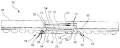
- FIG. 2it shows another integrated circuit device 50 embodying the present invention.
- the device 50is of the type which is referred to as a cavity down configuration wherein the device package includes a cavity 52 which receives the semiconductor substrate 54 therein.
- the semiconductor substrate 54is adhered to the package 56 with a suitable adhesive 58 .
- the package 56carries a substrate 60 .
- the substrate 60is preferably a multi-layered substrate providing conductive interconnect patterns.
- the substrate 60includes a first plurality of bonding pads 62 .
- the semiconductor substrate 54carries a second plurality of bonding pads 64 .
- the bonding pads of the semiconductor substrate 54are wire bonded to the bonding pads 62 of the substrate 60 by wire bonds 66 in a known manner.
- An interconnect substrate 70is carried by the semiconductor substrate 54 .
- the interconnect substrate 70is flip chip bonded to the semiconductor substrate 54 by a plurality of solder balls 72 . Wire bonds 67 also connect selected ones of pads 62 .
- the interconnect substrate 70may be multi-layered and in turn provide power supply and ground distribution within the semiconductor substrate 54 .
- the interconnect substrate 70carries a plurality of filter devices 74 in a known manner for filtering the power supply voltage.
- the filter devicesmay include discrete capacitors, inductors, and/or resistance.
- the assembly of the semiconductor substrate 54 and interconnection substrate 70is a delicate assembly which preferably is covered by a protective material or encapsulant 76 .
- the encapsulant 76may be deposited as a liquid and confined to a specific area by a further material forming a dam 78 in a manner well known in the art.
- the surface area of the interconnect substrate 70is smaller than the surface area of the semiconductor substrate 54 to provide peripheral areas 73 within which the bonding pads 64 of the semiconductor substrate are formed.
- the interconnection substratemay be utilized to distribute power and ground and in addition, any other critical signals requiring a low impedance path or special filtering.
- the power and ground and critical signalsmay be coupled to the interconnections of the interconnect substrate by the wire-bonding or the use of a conductive interconnect layer.
- integrated circuit devices structured in accordance with various aspects of the present inventionhave the dual effect of lowering the required substrate routing density on the package substrate while improving electrical performance of the device.
- the substrate wire density requirementis lessened by the wire bonding while the improved electrical performance is provided by the flip chip mounted interconnection substrates and optional use of discrete capacitors, resistors and devices. As a result, the combined benefit of excellent electrical performance and low cost is achieved.
Landscapes
- Engineering & Computer Science (AREA)
- Microelectronics & Electronic Packaging (AREA)
- Computer Hardware Design (AREA)
- Power Engineering (AREA)
- Physics & Mathematics (AREA)
- Condensed Matter Physics & Semiconductors (AREA)
- General Physics & Mathematics (AREA)
- Chemical & Material Sciences (AREA)
- Dispersion Chemistry (AREA)
- Semiconductor Integrated Circuits (AREA)
- Wire Bonding (AREA)
Abstract
Description
Claims (11)
Priority Applications (3)
| Application Number | Priority Date | Filing Date | Title |
|---|---|---|---|
| US10/678,495US7262508B2 (en) | 2003-10-03 | 2003-10-03 | Integrated circuit incorporating flip chip and wire bonding |
| DE102004030541ADE102004030541B4 (en) | 2003-10-03 | 2004-06-24 | Integrated circuit |
| JP2004283743AJP4813786B2 (en) | 2003-10-03 | 2004-09-29 | Integrated circuit and integrated circuit assembly |
Applications Claiming Priority (1)
| Application Number | Priority Date | Filing Date | Title |
|---|---|---|---|
| US10/678,495US7262508B2 (en) | 2003-10-03 | 2003-10-03 | Integrated circuit incorporating flip chip and wire bonding |
Publications (2)
| Publication Number | Publication Date |
|---|---|
| US20050073054A1 US20050073054A1 (en) | 2005-04-07 |
| US7262508B2true US7262508B2 (en) | 2007-08-28 |
Family
ID=34393949
Family Applications (1)
| Application Number | Title | Priority Date | Filing Date |
|---|---|---|---|
| US10/678,495Expired - LifetimeUS7262508B2 (en) | 2003-10-03 | 2003-10-03 | Integrated circuit incorporating flip chip and wire bonding |
Country Status (3)
| Country | Link |
|---|---|
| US (1) | US7262508B2 (en) |
| JP (1) | JP4813786B2 (en) |
| DE (1) | DE102004030541B4 (en) |
Cited By (3)
| Publication number | Priority date | Publication date | Assignee | Title |
|---|---|---|---|---|
| US20070164446A1 (en)* | 2006-01-13 | 2007-07-19 | Hawk Donald E Jr | Integrated circuit having second substrate to facilitate core power and ground distribution |
| US20140035114A1 (en)* | 2012-01-19 | 2014-02-06 | Semiconductor Components Industries, Llc | Semiconductor package structure and method |
| US20190157197A1 (en)* | 2017-11-22 | 2019-05-23 | Advanced Semiconductor Engineering, Inc. | Semiconductor device package |
Families Citing this family (2)
| Publication number | Priority date | Publication date | Assignee | Title |
|---|---|---|---|---|
| KR100763345B1 (en)* | 2006-08-30 | 2007-10-04 | 삼성전기주식회사 | Manufacturing Method of Electronic Circuit Board |
| CN110828496B (en)* | 2019-11-15 | 2022-10-11 | 华天科技(昆山)电子有限公司 | Semiconductor device and method for manufacturing the same |
Citations (13)
| Publication number | Priority date | Publication date | Assignee | Title |
|---|---|---|---|---|
| JPS589223A (en)* | 1981-07-10 | 1983-01-19 | Fujitsu Ltd | optical recording and reproducing device |
| US5646828A (en)* | 1995-02-24 | 1997-07-08 | Lucent Technologies Inc. | Thin packaging of multi-chip modules with enhanced thermal/power management |
| FR2758935A1 (en) | 1997-01-28 | 1998-07-31 | Matra Marconi Space France | Multiple layer casing for high frequency microelectronic circuit |
| US5798567A (en)* | 1997-08-21 | 1998-08-25 | Hewlett-Packard Company | Ball grid array integrated circuit package which employs a flip chip integrated circuit and decoupling capacitors |
| US6150724A (en)* | 1998-03-02 | 2000-11-21 | Motorola, Inc. | Multi-chip semiconductor device and method for making the device by using multiple flip chip interfaces |
| US6177725B1 (en) | 1995-10-24 | 2001-01-23 | Oki Electric Industry Co., Ltd. | Semiconductor device having an improved structure for preventing cracks, improved small-sized semiconductor and method of manufacturing the same |
| US6333564B1 (en)* | 1998-06-22 | 2001-12-25 | Fujitsu Limited | Surface mount type semiconductor device and method of producing the same having an interposing layer electrically connecting the semiconductor chip with protrusion electrodes |
| US6429530B1 (en) | 1998-11-02 | 2002-08-06 | International Business Machines Corporation | Miniaturized chip scale ball grid array semiconductor package |
| US20020130422A1 (en)* | 2001-03-15 | 2002-09-19 | Vaiyapuri Venkateshwaran | Semiconductor/printed circuit board assembly, and computer system |
| US6462420B2 (en)* | 1999-02-12 | 2002-10-08 | Rohm Co., Ltd. | Semiconductor chip and semiconductor device having a chip-on-chip structure |
| US6489686B2 (en)* | 1999-12-21 | 2002-12-03 | International Business Machines Corporation | Multi-cavity substrate structure for discrete devices |
| US20030222344A1 (en)* | 2002-05-30 | 2003-12-04 | Fujitsu Limited | Semiconductor device having a heat spreader exposed from a seal resin |
| US20040200885A1 (en)* | 2001-08-24 | 2004-10-14 | Derderian James M | Methods for assembling semiconductor devices in stacked arrangements by positioning spacers therebetween |
Family Cites Families (5)
| Publication number | Priority date | Publication date | Assignee | Title |
|---|---|---|---|---|
| JPH04127531A (en)* | 1990-09-19 | 1992-04-28 | Fujitsu Ltd | Semiconductor device and manufacture thereof |
| JPH05211279A (en)* | 1991-11-20 | 1993-08-20 | Nec Corp | Hybrid integrated circuit |
| JP3173308B2 (en)* | 1995-02-14 | 2001-06-04 | 住友金属工業株式会社 | Semiconductor integrated circuit device |
| JPH10321791A (en)* | 1997-03-17 | 1998-12-04 | Tokai Rika Co Ltd | Operational amplifier |
| US6683384B1 (en)* | 1997-10-08 | 2004-01-27 | Agere Systems Inc | Air isolated crossovers |
- 2003
- 2003-10-03USUS10/678,495patent/US7262508B2/ennot_activeExpired - Lifetime
- 2004
- 2004-06-24DEDE102004030541Apatent/DE102004030541B4/ennot_activeExpired - Fee Related
- 2004-09-29JPJP2004283743Apatent/JP4813786B2/ennot_activeExpired - Fee Related
Patent Citations (13)
| Publication number | Priority date | Publication date | Assignee | Title |
|---|---|---|---|---|
| JPS589223A (en)* | 1981-07-10 | 1983-01-19 | Fujitsu Ltd | optical recording and reproducing device |
| US5646828A (en)* | 1995-02-24 | 1997-07-08 | Lucent Technologies Inc. | Thin packaging of multi-chip modules with enhanced thermal/power management |
| US6177725B1 (en) | 1995-10-24 | 2001-01-23 | Oki Electric Industry Co., Ltd. | Semiconductor device having an improved structure for preventing cracks, improved small-sized semiconductor and method of manufacturing the same |
| FR2758935A1 (en) | 1997-01-28 | 1998-07-31 | Matra Marconi Space France | Multiple layer casing for high frequency microelectronic circuit |
| US5798567A (en)* | 1997-08-21 | 1998-08-25 | Hewlett-Packard Company | Ball grid array integrated circuit package which employs a flip chip integrated circuit and decoupling capacitors |
| US6150724A (en)* | 1998-03-02 | 2000-11-21 | Motorola, Inc. | Multi-chip semiconductor device and method for making the device by using multiple flip chip interfaces |
| US6333564B1 (en)* | 1998-06-22 | 2001-12-25 | Fujitsu Limited | Surface mount type semiconductor device and method of producing the same having an interposing layer electrically connecting the semiconductor chip with protrusion electrodes |
| US6429530B1 (en) | 1998-11-02 | 2002-08-06 | International Business Machines Corporation | Miniaturized chip scale ball grid array semiconductor package |
| US6462420B2 (en)* | 1999-02-12 | 2002-10-08 | Rohm Co., Ltd. | Semiconductor chip and semiconductor device having a chip-on-chip structure |
| US6489686B2 (en)* | 1999-12-21 | 2002-12-03 | International Business Machines Corporation | Multi-cavity substrate structure for discrete devices |
| US20020130422A1 (en)* | 2001-03-15 | 2002-09-19 | Vaiyapuri Venkateshwaran | Semiconductor/printed circuit board assembly, and computer system |
| US20040200885A1 (en)* | 2001-08-24 | 2004-10-14 | Derderian James M | Methods for assembling semiconductor devices in stacked arrangements by positioning spacers therebetween |
| US20030222344A1 (en)* | 2002-05-30 | 2003-12-04 | Fujitsu Limited | Semiconductor device having a heat spreader exposed from a seal resin |
Non-Patent Citations (1)
| Title |
|---|
| Office Action from related DE 10 2004 030 541.1-33 in English Translation & German Sep. 1, 2005. |
Cited By (5)
| Publication number | Priority date | Publication date | Assignee | Title |
|---|---|---|---|---|
| US20070164446A1 (en)* | 2006-01-13 | 2007-07-19 | Hawk Donald E Jr | Integrated circuit having second substrate to facilitate core power and ground distribution |
| US20140035114A1 (en)* | 2012-01-19 | 2014-02-06 | Semiconductor Components Industries, Llc | Semiconductor package structure and method |
| US9799627B2 (en)* | 2012-01-19 | 2017-10-24 | Semiconductor Components Industries, Llc | Semiconductor package structure and method |
| US20190157197A1 (en)* | 2017-11-22 | 2019-05-23 | Advanced Semiconductor Engineering, Inc. | Semiconductor device package |
| US10672696B2 (en)* | 2017-11-22 | 2020-06-02 | Advanced Semiconductor Engineering, Inc. | Semiconductor device package |
Also Published As
| Publication number | Publication date |
|---|---|
| JP4813786B2 (en) | 2011-11-09 |
| DE102004030541A1 (en) | 2005-05-12 |
| US20050073054A1 (en) | 2005-04-07 |
| JP2005117038A (en) | 2005-04-28 |
| DE102004030541B4 (en) | 2007-02-08 |
Similar Documents
| Publication | Publication Date | Title |
|---|---|---|
| KR100535181B1 (en) | Semiconductor chip package having decoupling capacitor and manufacturing method thereof | |
| US7259448B2 (en) | Die-up ball grid array package with a heat spreader and method for making the same | |
| US6664617B2 (en) | Semiconductor package | |
| US6020637A (en) | Ball grid array semiconductor package | |
| US6424050B1 (en) | Semiconductor device | |
| KR100480437B1 (en) | Semiconductor chip package stacked module | |
| US6611434B1 (en) | Stacked multi-chip package structure with on-chip integration of passive component | |
| US20090057867A1 (en) | Integrated Circuit Package with Passive Component | |
| KR950030321A (en) | Semiconductor device, manufacturing method and substrate | |
| JP2008243914A (en) | Semiconductor package and method of manufacturing the same | |
| JPH10270592A5 (en) | ||
| US8084868B1 (en) | Semiconductor package with fast power-up cycle and method of making same | |
| KR100429885B1 (en) | Multi-chip package improving heat spread characteristics and manufacturing method the same | |
| US8847412B2 (en) | Microelectronic assembly with thermally and electrically conductive underfill | |
| US6340839B1 (en) | Hybrid integrated circuit | |
| JP2001156251A (en) | Semiconductor device | |
| US20040058477A1 (en) | Integrated circuit package and manufacturing method therefor | |
| US7262508B2 (en) | Integrated circuit incorporating flip chip and wire bonding | |
| JP3312611B2 (en) | Film carrier type semiconductor device | |
| JP3093278B2 (en) | Electronic package with improved pad design | |
| KR20050027384A (en) | Chip size package having rerouting pad and stack thereof | |
| JPH04184962A (en) | Semiconductor integrated circuit device | |
| JPH02210858A (en) | Semiconductor device | |
| KR20040004798A (en) | Multi chip package | |
| JPH0670243U (en) | Circuit board device |
Legal Events
| Date | Code | Title | Description |
|---|---|---|---|
| AS | Assignment | Owner name:AGILENT TECHNOLOGIES, INC., COLORADO Free format text:ASSIGNMENT OF ASSIGNORS INTEREST;ASSIGNORS:KELLY, MICHAEL G.;KAW, RAVINDHAR K.;REEL/FRAME:014375/0700;SIGNING DATES FROM 20030617 TO 20030623 | |
| AS | Assignment | Owner name:AVAGO TECHNOLOGIES GENERAL IP PTE. LTD.,SINGAPORE Free format text:ASSIGNMENT OF ASSIGNORS INTEREST;ASSIGNOR:AGILENT TECHNOLOGIES, INC.;REEL/FRAME:017206/0666 Effective date:20051201 Owner name:AVAGO TECHNOLOGIES GENERAL IP PTE. LTD., SINGAPORE Free format text:ASSIGNMENT OF ASSIGNORS INTEREST;ASSIGNOR:AGILENT TECHNOLOGIES, INC.;REEL/FRAME:017206/0666 Effective date:20051201 | |
| AS | Assignment | Owner name:CITICORP NORTH AMERICA, INC.,DELAWARE Free format text:SECURITY AGREEMENT;ASSIGNOR:AVAGO TECHNOLOGIES GENERAL IP (SINGAPORE) PTE. LTD.;REEL/FRAME:017207/0882 Effective date:20051201 Owner name:CITICORP NORTH AMERICA, INC., DELAWARE Free format text:SECURITY AGREEMENT;ASSIGNOR:AVAGO TECHNOLOGIES GENERAL IP (SINGAPORE) PTE. LTD.;REEL/FRAME:017207/0882 Effective date:20051201 | |
| STCF | Information on status: patent grant | Free format text:PATENTED CASE | |
| FPAY | Fee payment | Year of fee payment:4 | |
| AS | Assignment | Owner name:AVAGO TECHNOLOGIES GENERAL IP (SINGAPORE) PTE. LTD Free format text:RELEASE BY SECURED PARTY;ASSIGNOR:CITICORP NORTH AMERICA, INC.;REEL/FRAME:030420/0048 Effective date:20110331 | |
| AS | Assignment | Owner name:DEUTSCHE BANK AG NEW YORK BRANCH, AS COLLATERAL AGENT, NEW YORK Free format text:PATENT SECURITY AGREEMENT;ASSIGNOR:AVAGO TECHNOLOGIES GENERAL IP (SINGAPORE) PTE. LTD.;REEL/FRAME:032851/0001 Effective date:20140506 Owner name:DEUTSCHE BANK AG NEW YORK BRANCH, AS COLLATERAL AG Free format text:PATENT SECURITY AGREEMENT;ASSIGNOR:AVAGO TECHNOLOGIES GENERAL IP (SINGAPORE) PTE. LTD.;REEL/FRAME:032851/0001 Effective date:20140506 | |
| FPAY | Fee payment | Year of fee payment:8 | |
| AS | Assignment | Owner name:AVAGO TECHNOLOGIES GENERAL IP (SINGAPORE) PTE. LTD., SINGAPORE Free format text:TERMINATION AND RELEASE OF SECURITY INTEREST IN PATENT RIGHTS (RELEASES RF 032851-0001);ASSIGNOR:DEUTSCHE BANK AG NEW YORK BRANCH, AS COLLATERAL AGENT;REEL/FRAME:037689/0001 Effective date:20160201 Owner name:AVAGO TECHNOLOGIES GENERAL IP (SINGAPORE) PTE. LTD Free format text:TERMINATION AND RELEASE OF SECURITY INTEREST IN PATENT RIGHTS (RELEASES RF 032851-0001);ASSIGNOR:DEUTSCHE BANK AG NEW YORK BRANCH, AS COLLATERAL AGENT;REEL/FRAME:037689/0001 Effective date:20160201 | |
| AS | Assignment | Owner name:BANK OF AMERICA, N.A., AS COLLATERAL AGENT, NORTH CAROLINA Free format text:PATENT SECURITY AGREEMENT;ASSIGNOR:AVAGO TECHNOLOGIES GENERAL IP (SINGAPORE) PTE. LTD.;REEL/FRAME:037808/0001 Effective date:20160201 Owner name:BANK OF AMERICA, N.A., AS COLLATERAL AGENT, NORTH Free format text:PATENT SECURITY AGREEMENT;ASSIGNOR:AVAGO TECHNOLOGIES GENERAL IP (SINGAPORE) PTE. LTD.;REEL/FRAME:037808/0001 Effective date:20160201 | |
| AS | Assignment | Owner name:AVAGO TECHNOLOGIES GENERAL IP (SINGAPORE) PTE. LTD Free format text:CORRECTIVE ASSIGNMENT TO CORRECT THE ASSIGNEE NAME PREVIOUSLY RECORDED AT REEL: 017206 FRAME: 0666. ASSIGNOR(S) HEREBY CONFIRMS THE ASSIGNMENT;ASSIGNOR:AGILENT TECHNOLOGIES, INC.;REEL/FRAME:038632/0662 Effective date:20051201 | |
| AS | Assignment | Owner name:AVAGO TECHNOLOGIES GENERAL IP (SINGAPORE) PTE. LTD., SINGAPORE Free format text:TERMINATION AND RELEASE OF SECURITY INTEREST IN PATENTS;ASSIGNOR:BANK OF AMERICA, N.A., AS COLLATERAL AGENT;REEL/FRAME:041710/0001 Effective date:20170119 Owner name:AVAGO TECHNOLOGIES GENERAL IP (SINGAPORE) PTE. LTD Free format text:TERMINATION AND RELEASE OF SECURITY INTEREST IN PATENTS;ASSIGNOR:BANK OF AMERICA, N.A., AS COLLATERAL AGENT;REEL/FRAME:041710/0001 Effective date:20170119 | |
| AS | Assignment | Owner name:AVAGO TECHNOLOGIES INTERNATIONAL SALES PTE. LIMITE Free format text:MERGER;ASSIGNOR:AVAGO TECHNOLOGIES GENERAL IP (SINGAPORE) PTE. LTD.;REEL/FRAME:047196/0097 Effective date:20180509 | |
| MAFP | Maintenance fee payment | Free format text:PAYMENT OF MAINTENANCE FEE, 12TH YEAR, LARGE ENTITY (ORIGINAL EVENT CODE: M1553); ENTITY STATUS OF PATENT OWNER: LARGE ENTITY Year of fee payment:12 | |
| AS | Assignment | Owner name:AVAGO TECHNOLOGIES INTERNATIONAL SALES PTE. LIMITE Free format text:CORRECTIVE ASSIGNMENT TO CORRECT THE EXECUTION DATE PREVIOUSLY RECORDED AT REEL: 047196 FRAME: 0097. ASSIGNOR(S) HEREBY CONFIRMS THE MERGER;ASSIGNOR:AVAGO TECHNOLOGIES GENERAL IP (SINGAPORE) PTE. LTD.;REEL/FRAME:048555/0510 Effective date:20180905 | |
| AS | Assignment | Owner name:BROADCOM INTERNATIONAL PTE. LTD., SINGAPORE Free format text:ASSIGNMENT OF ASSIGNORS INTEREST;ASSIGNOR:AVAGO TECHNOLOGIES INTERNATIONAL SALES PTE. LIMITED;REEL/FRAME:053771/0901 Effective date:20200826 | |
| AS | Assignment | Owner name:AVAGO TECHNOLOGIES INTERNATIONAL SALES PTE. LIMITED, SINGAPORE Free format text:MERGER;ASSIGNORS:AVAGO TECHNOLOGIES INTERNATIONAL SALES PTE. LIMITED;BROADCOM INTERNATIONAL PTE. LTD.;REEL/FRAME:062952/0850 Effective date:20230202 |