US7262134B2 - Microfeature workpieces and methods for forming interconnects in microfeature workpieces - Google Patents
Microfeature workpieces and methods for forming interconnects in microfeature workpiecesDownload PDFInfo
- Publication number
- US7262134B2 US7262134B2US11/218,243US21824305AUS7262134B2US 7262134 B2US7262134 B2US 7262134B2US 21824305 AUS21824305 AUS 21824305AUS 7262134 B2US7262134 B2US 7262134B2
- Authority
- US
- United States
- Prior art keywords
- substrate
- hole
- dielectric layer
- forming
- section
- Prior art date
- Legal status (The legal status is an assumption and is not a legal conclusion. Google has not performed a legal analysis and makes no representation as to the accuracy of the status listed.)
- Expired - Lifetime
Links
Images


Classifications
- H—ELECTRICITY
- H01—ELECTRIC ELEMENTS
- H01L—SEMICONDUCTOR DEVICES NOT COVERED BY CLASS H10
- H01L21/00—Processes or apparatus adapted for the manufacture or treatment of semiconductor or solid state devices or of parts thereof
- H01L21/70—Manufacture or treatment of devices consisting of a plurality of solid state components formed in or on a common substrate or of parts thereof; Manufacture of integrated circuit devices or of parts thereof
- H01L21/71—Manufacture of specific parts of devices defined in group H01L21/70
- H01L21/768—Applying interconnections to be used for carrying current between separate components within a device comprising conductors and dielectrics
- H01L21/76898—Applying interconnections to be used for carrying current between separate components within a device comprising conductors and dielectrics formed through a semiconductor substrate
- H—ELECTRICITY
- H01—ELECTRIC ELEMENTS
- H01L—SEMICONDUCTOR DEVICES NOT COVERED BY CLASS H10
- H01L21/00—Processes or apparatus adapted for the manufacture or treatment of semiconductor or solid state devices or of parts thereof
- H01L21/70—Manufacture or treatment of devices consisting of a plurality of solid state components formed in or on a common substrate or of parts thereof; Manufacture of integrated circuit devices or of parts thereof
- H01L21/71—Manufacture of specific parts of devices defined in group H01L21/70
- H01L21/768—Applying interconnections to be used for carrying current between separate components within a device comprising conductors and dielectrics
- H01L21/76838—Applying interconnections to be used for carrying current between separate components within a device comprising conductors and dielectrics characterised by the formation and the after-treatment of the conductors
- H01L21/76841—Barrier, adhesion or liner layers
- H01L21/76868—Forming or treating discontinuous thin films, e.g. repair, enhancement or reinforcement of discontinuous thin films
- H—ELECTRICITY
- H01—ELECTRIC ELEMENTS
- H01L—SEMICONDUCTOR DEVICES NOT COVERED BY CLASS H10
- H01L21/00—Processes or apparatus adapted for the manufacture or treatment of semiconductor or solid state devices or of parts thereof
- H01L21/70—Manufacture or treatment of devices consisting of a plurality of solid state components formed in or on a common substrate or of parts thereof; Manufacture of integrated circuit devices or of parts thereof
- H01L21/71—Manufacture of specific parts of devices defined in group H01L21/70
- H01L21/768—Applying interconnections to be used for carrying current between separate components within a device comprising conductors and dielectrics
- H01L21/76838—Applying interconnections to be used for carrying current between separate components within a device comprising conductors and dielectrics characterised by the formation and the after-treatment of the conductors
- H01L21/76841—Barrier, adhesion or liner layers
- H01L21/76871—Layers specifically deposited to enhance or enable the nucleation of further layers, i.e. seed layers
- H01L21/76873—Layers specifically deposited to enhance or enable the nucleation of further layers, i.e. seed layers for electroplating
- H—ELECTRICITY
- H01—ELECTRIC ELEMENTS
- H01L—SEMICONDUCTOR DEVICES NOT COVERED BY CLASS H10
- H01L23/00—Details of semiconductor or other solid state devices
- H01L23/48—Arrangements for conducting electric current to or from the solid state body in operation, e.g. leads, terminal arrangements ; Selection of materials therefor
- H01L23/481—Internal lead connections, e.g. via connections, feedthrough structures
- H—ELECTRICITY
- H01—ELECTRIC ELEMENTS
- H01L—SEMICONDUCTOR DEVICES NOT COVERED BY CLASS H10
- H01L2924/00—Indexing scheme for arrangements or methods for connecting or disconnecting semiconductor or solid-state bodies as covered by H01L24/00
- H01L2924/0001—Technical content checked by a classifier
- H01L2924/0002—Not covered by any one of groups H01L24/00, H01L24/00 and H01L2224/00
Definitions
- the present inventionrelates to methods for forming interconnects in microfeature workpieces and microfeature workpieces formed using such methods.
- Microelectronic devices, micromechanical devices, and other devices with microfeaturesare typically formed by constructing several layers of components on a workpiece.
- a plurality of diesare fabricated on a single workpiece, and each die generally includes an integrated circuit and a plurality of bond-pads coupled to the integrated circuit.
- the diesare separated from each other and packaged to form individual microelectronic devices that can be attached to modules or installed in other products.
- interconnectsthat electrically couple conductive components located in different layers.
- Such interconnectselectrically couple bond-pads or other conductive elements proximate to one side of the dies to conductive elements proximate to the other side of the dies.
- Through-wafer interconnectsare constructed by forming deep vias on the front side and/or backside of the workpiece and in alignment with corresponding bond-pads at the front side of the workpiece.
- the viasare often blind vias in that they are closed at one end.
- the blind viasare then filled with a conductive fill material.
- solder balls or other external electrical contactsare subsequently attached to the through-wafer interconnects at the backside and/or the front side of the workpiece.
- the solder balls or external contactscan be attached either before or after singulating the dies from the workpiece.
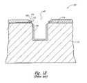
- FIGS. 1A-1Cillustrate a conventional process of forming a through-wafer interconnect.
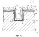
- FIG. 1Ais a schematic side cross-sectional view of a workpiece 100 including a substrate 112 , a terminal 122 on the substrate 112 , and a hole 145 extending through the terminal 122 and into the substrate 112 .
- a dielectric layer 134is deposited across the workpiece 100 and into the hole 145 to insulate the substrate 112 from the conductive material of the interconnect.
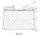
- FIG. 1Billustrates the workpiece 100 after removing a portion of the dielectric layer 134 with a spacer etching process. This process sometimes exposes a section 115 of an upper surface 114 on the substrate 112 .
- FIG. 1Cillustrates the workpiece 100 after forming a conductive interconnect 182 in the hole 145 with the interconnect 182 contacting the terminal 122 . If the substrate 112 includes an exposed section 115 , the interconnect 182 may also contact the substrate 112 and create a short between the terminal 122 and the substrate 112 . Therefore, there is a need to improve the process of forming interconnects in workpieces.
- FIGS. 1A-1Cillustrate a conventional process of forming an electrically conductive interconnect in accordance with the prior art.
- FIGS. 2A-2Qare side cross-sectional views illustrating stages of a method for forming electrically conductive interconnects in a microfeature workpiece in accordance with an embodiment of the invention.
- FIGS. 3A-3Gare side cross-sectional views illustrating stages of a method for forming electrically conductive interconnects in a microfeature workpiece in accordance with another embodiment of the invention.
- One aspect of the inventionis directed to methods of forming an interconnect in a microfeature workpiece having a substrate, a terminal, and a dielectric layer between the substrate and the terminal.
- An embodiment of one such methodincludes forming a hole extending through the terminal and the dielectric layer to at least an intermediate depth in the substrate. The hole has a first lateral dimension in the dielectric layer and a second lateral dimension in the substrate proximate to an interface between the dielectric layer and the substrate. The second lateral dimension is greater than the first lateral dimension.
- the methodfurther includes constructing an electrically conductive interconnect in at least a portion of the hole and in electrical contact with the terminal.
- the holecan be formed by etching the substrate in a first cycle for a first time period to form a first section of the hole in the substrate, and etching the substrate in a second cycle for a second time period to form a second section of the hole in the substrate.
- the second time periodis less than the first time period.
- the holecan be formed by (a) selectively removing a portion of the dielectric layer and a first portion of the substrate with a first process, and (b) selectively removing a second portion of the substrate with a second process.
- the holecan be constructed such that the dielectric layer overhangs a section of the hole in the substrate at the interface between the dielectric layer and the substrate.
- the workpieceincludes an undercut in the substrate at the interface between the dielectric layer and the substrate.
- a methodin another embodiment, includes (a) providing a microfeature workpiece having a substrate, a dielectric layer on the substrate, and a terminal on the dielectric layer, (b) forming a hole in the terminal of the workpiece, and (c) removing a portion of the dielectric layer and a portion of the substrate in a single, generally continuous process.
- the portion of the dielectric layer and the portion of the substrateare generally aligned with the hole in the terminal and can be removed by etching or other suitable processes.
- a microfeature workpieceincludes a substrate, a dielectric layer on the substrate, a terminal on the dielectric layer, an operable microelectronic feature carried by the substrate and operably coupled to the terminal, and an interconnect via extending through the terminal and the dielectric layer to at least an intermediate depth in the substrate.
- the interconnect viaincludes an undercut portion in the substrate at an interface between the dielectric layer and the substrate.
- the interconnect viacan have a first lateral dimension in the dielectric layer and a second lateral dimension in the substrate at an interface between the dielectric layer and the substrate. The second lateral dimension is greater than the first lateral dimension.
- the microfeature workpiececan further include an electrically conductive interconnect in the interconnect via and in contact with the terminal.
- microfeature workpieceis used throughout to include substrates upon which and/or in which microelectronic devices, micromechanical devices, data storage elements, optics, and other features are fabricated.
- microfeature workpiecescan be semiconductor wafers, glass substrates, dielectric substrates, or many other types of substrates.
- Many features on such microfeature workpieceshave critical dimensions less than or equal to 1 ⁇ m, and in many applications the critical dimensions of the smaller features are less than 0.25 ⁇ m or even less than 0.1 ⁇ m. Where the context permits, singular or plural terms may also include the plural or singular term, respectively.
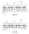
- FIGS. 2A-2Qillustrate stages of a method for forming interconnects in a microfeature workpiece 200 in accordance with an embodiment of the invention.
- FIG. 2Ais a side cross-sectional view of a portion of the workpiece 200 at an initial stage before the interconnects have been formed.
- the workpiece 200can include a substrate 212 and a plurality of microelectronic dies 220 formed in and/or on the substrate 212 .
- the substrate 212has a first side 214 and a second side 216 opposite the first side 214 .
- the substrate 212is generally a semiconductor wafer, and the dies 220 are arranged in a die pattern on the wafer.
- the individual dies 220include integrated circuitry 221 (shown schematically) and a plurality of terminals 222 (e.g., bond-pads) electrically coupled to the integrated circuitry 221 .
- the terminals 222 shown in FIG. 2Aare external features at the first side 214 of the substrate 212 . In other embodiments, however, the terminals 222 can be internal features that are embedded at an intermediate depth within the substrate 212 .
- FIG. 2Bis a side cross-sectional view of the area 2 B shown in FIG. 2A .
- a first dielectric layer 230was applied to the first side 214 of the substrate 212
- a second dielectric layer 232was applied over the first dielectric layer 230 .
- the second dielectric layer 232was then patterned and etched to expose the terminal 222 .
- the dielectric layers 230 and 232can be a polyimide material or other suitable nonconductive materials.
- the dielectric layers 230 and 232can be parylene, a low temperature chemical vapor deposition (low temperature CVD) material such as silicon nitride (Si 3 N 4 ), silicon oxide (SiO 2 ), and/or other suitable materials.
- low temperature CVDlow temperature chemical vapor deposition
- the dielectric layers 230 and 232are generally not composed of the same material as each other, but these layers may be composed of the same material. In addition, one or both of the layers 230 and 232 may be omitted and/or additional layers may be included.
- a mask 233is applied over the second dielectric layer 232 and patterned as shown in FIG. 2B .
- the mask 233can be a layer of resist that is patterned according to the arrangement of terminals 222 on the workpiece 200 . As such, the mask 233 has an opening over the terminal 222 .
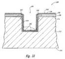
- a first hole section 245 ahas been formed through the terminal 222 .
- the first hole section 245 acan be formed using a wet etching or dry etching process that selectively removes material from the terminal 222 and generally does not remove material from the first dielectric layer 230 .
- the first dielectric layer 230can accordingly be an etch-stop.
- the etching processcan be repeated until the first hole section 245 a extends through the terminal 222 .
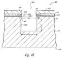
- a second hole section 245 b(identified as 245 ′ and 245 b ′′) has been formed in the first dielectric layer 230 and the substrate 212 .
- the second hole section 245 bhas a first portion 245 b ′ that extends through the first dielectric layer 230 and a second portion 245 b ′′ that extends from the interface of the substrate 212 and the first dielectric layer 230 to a first depth T 1 in the substrate 212 .
- the first portion 245 b ′has a first diameter D 1 and is generally aligned with the first hole section 245 a in the terminal 222 .
- the second portion 245 b ′′has a second diameter D 2 at the interface of the substrate 212 and the first dielectric layer 230 .
- the second diameter D 2is greater than the first diameter D 1 such that the second portion 245 b ′′ forms an undercut portion 247 in the substrate 212 below the first dielectric layer 230 and exposes a portion of a back surface 231 of the first dielectric layer 230 .
- the first dielectric layer 230forms an overhang over the second portion 245 b′′.
- the second hole section 245 bis formed in a single, generally continuous process.
- the second hole section 245 bcan be formed in a single dry oxide etch process that, due to the nature of the etchant, tends to anistropically etch the first dielectric layer 230 and isotropically etch the substrate 212 .
- the second etching process for the first dielectric layer 230 and the upper portion of the substrate 212can be different than the first etching process for the terminal 222 .
- the second etching processcan selectively remove material from the first dielectric layer 230 and the substrate 212 at a higher etch rate than from the terminal 222 .
- the second etching processaccordingly does not significantly alter the general structure of the terminal 222 .
- the first and second hole sections 245 a - bcan be formed using a single etching process.
- Table 1illustrates one example of a recipe for a suitable second etching process to remove material from the first dielectric layer 230 and the upper portion of the substrate 212 .
- Step 1Step end control BY TIME Maximum step time 7 seconds Pressure SERVO 200 MTORR RF power, match, mode 0 W, AUTO, RF OFF Helium Pressure 9000 AR 50 sccm CF4 50 sccm CHF3 25 sccm NF3 45 sccm Step 2 Step end control BY TIME Maximum step time 20 seconds Pressure SERVO 200 MTORR RF power, match, mode 1050 W, AUTO, B-to-B Helium Pressure 9000 AR 50 sccm CF4 50 sccm CHF3 20 sccm NF3 45 sccm Step 3 Step end control BY TIME Maximum step time 330 seconds Pressure SERVO 200 MTORR RF power, match, mode 1050 W, AUTO, RF OFF Helium Pressure 9000 AR 50 sccm CF4 70 sccm CHF3 20 sccm NF3 20 sccm
- a third hole section 245 chas been formed in the substrate 212 .
- the third hole section 245 chas a third diameter D 3 that can be greater than, less than, or equal to the second diameter D 2 .
- the third diameter D 3 of the third hole section 245 cis generally a function of the available real estate and processing parameters for subsequent stages.
- the third hole section 245 cextends a second depth T 2 into the substrate 212 that is greater than the first depth T 1 .
- first, second, and third hole sections 245 a - cdefine a blind hole 245 that extends through only a portion of the workpiece 200 and is closed at one end, in other embodiments the hole 245 can be through hole that extends completely through the workpiece 200 .
- the illustrated third hole section 245 cis formed by etching the substrate 212 using one or more individual etches, such as a deep silicon etch. After forming the third hole section 245 c , the mask 233 is removed from the workpiece 200 .
- the third hole section 245 ccan alternatively be formed using laser ablation in addition to or in lieu of etching. If a laser is used to form all or a portion of the third hole section 245 c , the hole 245 is typically cleaned using chemical cleaning agents to remove slag and/or other contaminants.
- Etching the entire hole 245may be easier than laser cutting because the slag does not need to be cleaned from the hole 245 and, in applications in which the hole 245 is a blind hole, the depth of the hole 245 can be more precisely controlled with an etching process.
- blind holescan generally be more precisely aligned using an etching process than a laser cutting process.
- a further advantage of using an etching processis that the first side 214 of the substrate 212 can be patterned and etched to simultaneously form a plurality of holes 245 aligned with corresponding terminals 222 .
- a third dielectric layer 234is deposited onto the workpiece 200 to line the sidewalls of the hole 245 in the substrate 212 .
- the third dielectric layer 234electrically insulates components in the substrate 212 from an interconnect that is subsequently formed in the hole 245 .
- the third dielectric layer 234can be an ALD (atomic layer deposition) aluminum oxide material applied using a suitable deposition process or another suitable low temperature CVD oxide.
- the third dielectric layer 234can include a silane-based and/or an aluminum-based oxide material.
- the third dielectric layer 234can include other suitable dielectric materials.
- a suitable etching processe.g., a spacer etch
- a diffusion barrier layer 236is then deposited onto the workpiece 200 over the third dielectric layer 234 in the hole 245 and is in electrical contact with the terminal 222 .
- the barrier layer 236generally covers the second dielectric layer 232 and the terminal 222 in addition to the third dielectric layer 234 .
- the barrier layer 236is a layer of tantalum that is deposited onto the workpiece 200 using physical vapor deposition (PVD).
- PVDphysical vapor deposition
- the thickness of the barrier layer 236is about 150 Angstroms.
- the barrier layer 236may be deposited onto the workpiece 200 using other vapor deposition processes, such as CVD, and/or may have a different thickness.
- the barrier layer 236is not limited to tantalum, but rather may be composed of tungsten or other suitable materials that help contain the fill material subsequently deposited into the hole 245 .
- a seed layer 250is deposited onto the barrier layer 236 .
- the seed layer 250can be deposited using vapor deposition techniques, such as PVD, CVD, atomic layer deposition, and/or plating.
- the seed layer 250can be composed of Cu or other suitable materials.
- the thickness of the seed layer 250may be about 2000 Angstroms, but could be more or less depending upon the depth and aspect ratio of the hole 245 .
- the seed layer 250may not uniformly cover the barrier layer 236 such that the seed layer 250 has voids 251 within the hole 245 . This can cause non-uniform electroplating in the hole 245 and across the workpiece 200 .
- the seed layer 250When the seed layer 250 is deficient, it is preferably enhanced using a process that fills voids or noncontinuous regions of the seed layer 250 to form a more uniform seed layer. Referring to FIG. 2J , for example, voids 251 and/or noncontinuous regions of the seed layer 250 have been filled with additional material 252 , such as copper or another suitable material.
- additional material 252such as copper or another suitable material.
- a resist layer 260is deposited onto the seed layer 250 and patterned to have an opening 261 over the terminal 222 and corresponding hole 245 .
- a first conductive layer 254is then deposited onto the exposed portions of the seed layer 250 in the hole 245 .
- the first conductive layer 254can be Cu that is deposited onto the seed layer 250 in an electroless plating operation, electroplating operation, or another suitable method.
- the thickness of the first conductive layer 254is about 1 micron. In other embodiments, the first conductive layer 254 may include other suitable materials and/or have a different thickness.
- a second conductive layer 256is deposited onto the first conductive layer 254 in the hole 245 .
- the second conductive layer 256is a wetting agent that facilitates depositing subsequent materials into the hole 245 .
- the second conductive layer 256can be Ni that is deposited onto the first conductive layer 254 using an electroless or electrolytic plating process.
- the thickness of the second conductive layer 256is approximately 3-5 microns.
- the hole 245may be coated with other suitable materials using other methods and/or have a different thickness.
- a vent hole 270is formed in the substrate 212 extending from a bottom portion of the hole 245 to the second side 216 of the substrate 212 .
- the vent hole 270can be formed using a laser to cut through the substrate 212 from the second side 216 to the bottom of the hole 245 .
- the lasercan be aligned with the hole 245 and/or corresponding terminal 222 using scanning/alignment systems known in the art.
- a suitable laseris the Xise200 commercially available from Xsil Ltd. of Dublin, Ireland.
- the hole 270is generally cleaned to remove ablated byproducts (i.e., slag) and/or other undesirable byproducts resulting from the laser.
- the vent hole 270can be cleaned using a suitable cleaning agent, such as 6% tetramethylammonium hydroxide (TMAH): propylene glycol.
- TMAH6% tetramethylammonium hydroxide
- the vent hole 270may not be cleaned.
- the vent hole 270can be a different size or shape, and may be formed using an etching process (e.g., a dry etch and/or a wet etch), a mechanical drilling process, a dicing or laser slot, or another suitable method.
- the substratemay not include a vent hole.
- a temporary protective filling or coating 269(shown in broken lines) can be deposited into the hole 245 before forming the vent hole 270 .
- the protective filling 269can be a photoresist, a polymer, water, a solidified liquid or gas, or another suitable material.
- the protective filling 269protects the sidewalls of the hole 245 from slag produced during the laser drilling process. The slag can negatively affect the plating of Ni onto the seed layer 250 and/or the wetting of a conductive fill material into the hole 245 .
- the protective filling 269can be removed after forming the vent hole 270 .
- a conductive fill material 280is deposited into the hole 245 to form an interconnect 282 .
- the interconnect 282has a first end 283 proximate to the terminal 222 and a second end 284 at the bottom of the hole 245 .
- the fill material 280can include Cu, Ni, Co, Ag, Au, SnAgCu solder, AuSn solder, a solder having another composition, or other suitable materials or alloys of materials having the desired conductivity.
- the conductive fill material 280can be deposited into the blind hole 245 using plating processes, solder wave processes, screen printing processes, reflow processes, vapor deposition processes, or other suitable techniques.
- the plating processesfor example, can be electroless plating processes or electroplating processes.
- the barrier layer 236 and/or seed layer 250can be used as electroplating contacts.
- the resist layer 260is removed from the workpiece 200 and a suitable etching process is used to remove the remaining portions of the seed layer 250 and the barrier layer 236 on the first surface 235 of the second dielectric layer 232 .
- a first surface 201 of the workpiece 200can then be planarized using grinding, chemical-mechanical planarization (CMP), and/or other suitable processes.
- FIG. 2Pis a side cross-sectional view of the workpiece 200 with multiple interconnects 282 formed at corresponding terminals 222 of the dies 220 .
- the workpiece 200can be thinned to a desired thickness T to expose the second ends 284 of the interconnects 282 .
- the initial thickness of the substrate 212is approximately 750 microns
- the final thickness Tis approximately 100-500 microns.
- the initial and final thicknessescan be different in other embodiments.
- the second side 216 of the substrate 212can be thinned by grinding, dry etching, chemical etching, chemical polishing, CMP, or other suitable processes.
- undercutting into a substrate when forming a through-wafer interconnect holewas undesirable for several reasons.
- Undercutting into the substrateincreased the time necessary to etch through the oxide or first dielectric layer.
- the undercutwas difficult to cover with dielectric material and increased the likelihood that the interconnect would contact the substrate and cause a short.
- Third, the undercutcould collect containments that cause defects in the devices. As a result, conventional processes of forming through-wafer interconnects did not include undercutting the substrate.
- one advantage of several embodiments of the method for forming interconnects 282 illustrated in FIGS. 2A-2Qis that the resulting interconnect 282 is electrically isolated from the substrate 212 .
- the illustrated methodforms a hole 245 with an undercut portion 247 at the interface of the first dielectric layer 230 and the substrate 212 , and deposits a third dielectric layer 234 in the hole 245 .
- the portion of the third dielectric layer 234 in the undercut portion 247 of the hole 245is either not removed or the removed material is insufficient to expose the substrate 212 . Because the portion of the substrate 212 in the hole 245 is covered by the third dielectric layer 234 and not exposed, the substrate 212 is electrically isolated from the interconnect 282 , which prevents shorting between the substrate 212 and the terminal 222 .
- the method illustrated in FIGS. 2A-2Qforms an interconnect 282 that is electrically isolated from the substrate 212 without significantly increasing the processing time.
- the processing timeis expected to be faster than the time required in conventional methods because the time spent forming the undercut portion 247 reduces the time required to form the remainder of the hole 245 in the substrate 212 .
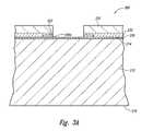
- FIGS. 3A-3Gillustrate stages in a method for forming interconnects in a microfeature workpiece 300 in accordance with another embodiment of the invention.
- FIG. 3Ais a side cross-sectional view of a portion of the workpiece 300 at an initial stage before the interconnects have been formed.
- first and second dielectric layers 230 and 232have been deposited onto the substrate 212 , and a first hole section 345 a has been formed through the terminal 222 .
- the first dielectric layer 230 directly beneath the terminal 222is etched to expose at least a portion of the substrate 212 and form a second hole section 345 b generally aligned with the first hole section 345 a .
- the second etching process for removing material from the first dielectric layer 230can be different than the first etching process for removing material from the terminal 222 .
- the second etching processcan selectively remove material from the first dielectric layer 230 at a higher etch rate than from either the terminal 222 or the substrate 212 .
- the second etching processaccordingly does not significantly alter the general structure of the terminal 222 or the substrate 212 . In other embodiments, however, material can be removed from the terminal 222 and the first dielectric layer 230 in a single etching process.
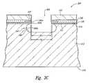
- FIGS. 3C-3Gillustrate a technique, typically referred to as a Bosch process, for forming a hole 345 in the substrate 212 .
- the mask 233is used again on the workpiece 300 to form a third hole section 345 c through a portion of the substrate 212 in a first etching cycle.
- the second hole section 345 bhas a first diameter D 1
- the third hole section 345 chas a second diameter D 2 at the interface between the first dielectric layer 230 and the substrate 212 .
- the second diameter D 2is greater than the first diameter D 1 such that the third hole section 345 c forms an undercut portion 347 in the substrate 212 below the first dielectric layer 230 and exposes a back surface 231 of the first dielectric layer 230 .
- the first dielectric layer 230forms an overhang over the third hole section 345 c .
- the first etching cycleforms a generally cylindrical sidewall 349 that has a barrel-type shape (exaggerated in the figures for purposes of illustration).
- a third dielectric layer 342is formed on the sidewall 349 to passivate the third hole section 345 c in the substrate 212 .
- the third dielectric layer 342can be a teflon-like polymer or other suitable materials. The third dielectric layer 342 accordingly inhibits the third hole section 345 c from becoming further widened as the hole 345 is deepened.
- a fourth hole section 345 dhas been formed in the substrate 212 below the third hole section 345 c by a second etching cycle.
- the third hole section 345 chas a third major lateral dimension D 3 and a third depth T 3
- the fourth hole section 345 dhas a fourth major lateral dimension D 4 less than the third major lateral dimension D 3 and a fourth depth T 4 less than the third depth T 3 .
- the second etching cyclehas different process parameters than the first etching cycle that formed the third hole section 345 c .
- the first etching cyclecan include exposing the substrate 212 to an etchant (e.g., SF 6 ) for a first process time
- the second etching cyclecan include exposing the substrate 212 to the etchant for a second process time less than the first process time.
- the first and second etching cyclescan have the same exposure time but use different etchants or vary other process parameters.
- the first and second etching cyclescan be generally the same, and the third and fourth hole sections 345 c - d have generally the same size.
- the third dielectric layer 342is again applied to coat the newly formed fourth hole section 345 d and inhibit the section 345 d from becoming further widened as the hole 345 is deepened.
- a fifth hole section 345 ehas been formed in the substrate 212 below the fourth hole section 345 d by a third etching cycle.
- the fifth hole section 345 ehas a fifth major lateral dimension D 5 generally the same as the fourth major lateral dimension D 4 of the fourth hole section 345 d , and a fifth depth T 5 generally the same as the fourth depth T 4 .
- the third etching cyclecan be accordingly generally the same as the second etching cycle.
- the process of applying the dielectric layer 342 to the newly formed hole section and then etching an additional hole section in the substrate 212can be repeated until the hole 345 extends to a desired depth in the substrate 212 .
- an interconnectcan be formed in the hole 345 as described above with reference to FIGS. 2H-2Q .
Landscapes
- Engineering & Computer Science (AREA)
- Physics & Mathematics (AREA)
- Condensed Matter Physics & Semiconductors (AREA)
- General Physics & Mathematics (AREA)
- Computer Hardware Design (AREA)
- Microelectronics & Electronic Packaging (AREA)
- Power Engineering (AREA)
- Manufacturing & Machinery (AREA)
- Internal Circuitry In Semiconductor Integrated Circuit Devices (AREA)
Abstract
Description
| TABLE 1 | |||
| Step 1 | |||
| Step end control | BY TIME | ||
| Maximum step time | 7 | ||
| Pressure | SERVO | ||
| 200 MTORR | |||
| RF power, match, mode | 0 W, AUTO, RF OFF | ||
| Helium Pressure | 9000 | ||
| AR | 50 sccm | ||
| CF4 | 50 sccm | ||
| CHF3 | 25 sccm | ||
| NF3 | 45 sccm | ||
| Step 2 | |||
| Step end control | BY TIME | ||
| 20 | |||
| Pressure | SERVO | ||
| 200 MTORR | |||
| RF power, match, mode | 1050 W, AUTO, B-to-B | ||
| Helium Pressure | 9000 | ||
| AR | 50 sccm | ||
| CF4 | 50 sccm | ||
| CHF3 | 20 sccm | ||
| NF3 | 45 sccm | ||
| Step 3 | |||
| Step end control | BY TIME | ||
| Maximum step time | 330 | ||
| Pressure | SERVO | ||
| 200 MTORR | |||
| RF power, match, mode | 1050 W, AUTO, RF OFF | ||
| Helium Pressure | 9000 | ||
| AR | 50 sccm | ||
| CF4 | 70 sccm | ||
| CHF3 | 20 sccm | ||
| NF3 | 20 sccm | ||
Claims (32)
Priority Applications (3)
| Application Number | Priority Date | Filing Date | Title |
|---|---|---|---|
| US11/218,243US7262134B2 (en) | 2005-09-01 | 2005-09-01 | Microfeature workpieces and methods for forming interconnects in microfeature workpieces |
| PCT/US2006/034153WO2007027973A2 (en) | 2005-09-01 | 2006-09-01 | Microfeature workpieces and methods for forming interconnects in microfeature workpieces |
| US11/832,742US7915736B2 (en) | 2005-09-01 | 2007-08-02 | Microfeature workpieces and methods for forming interconnects in microfeature workpieces |
Applications Claiming Priority (1)
| Application Number | Priority Date | Filing Date | Title |
|---|---|---|---|
| US11/218,243US7262134B2 (en) | 2005-09-01 | 2005-09-01 | Microfeature workpieces and methods for forming interconnects in microfeature workpieces |
Related Child Applications (1)
| Application Number | Title | Priority Date | Filing Date |
|---|---|---|---|
| US11/832,742DivisionUS7915736B2 (en) | 2005-09-01 | 2007-08-02 | Microfeature workpieces and methods for forming interconnects in microfeature workpieces |
Publications (2)
| Publication Number | Publication Date |
|---|---|
| US20070045858A1 US20070045858A1 (en) | 2007-03-01 |
| US7262134B2true US7262134B2 (en) | 2007-08-28 |
Family
ID=37802945
Family Applications (2)
| Application Number | Title | Priority Date | Filing Date |
|---|---|---|---|
| US11/218,243Expired - LifetimeUS7262134B2 (en) | 2005-09-01 | 2005-09-01 | Microfeature workpieces and methods for forming interconnects in microfeature workpieces |
| US11/832,742Active2026-08-29US7915736B2 (en) | 2005-09-01 | 2007-08-02 | Microfeature workpieces and methods for forming interconnects in microfeature workpieces |
Family Applications After (1)
| Application Number | Title | Priority Date | Filing Date |
|---|---|---|---|
| US11/832,742Active2026-08-29US7915736B2 (en) | 2005-09-01 | 2007-08-02 | Microfeature workpieces and methods for forming interconnects in microfeature workpieces |
Country Status (2)
| Country | Link |
|---|---|
| US (2) | US7262134B2 (en) |
| WO (1) | WO2007027973A2 (en) |
Cited By (23)
| Publication number | Priority date | Publication date | Assignee | Title |
|---|---|---|---|---|
| US7413979B2 (en) | 2003-11-13 | 2008-08-19 | Micron Technology, Inc. | Methods for forming vias in microelectronic devices, and methods for packaging microelectronic devices |
| US7425499B2 (en) | 2004-08-24 | 2008-09-16 | Micron Technology, Inc. | Methods for forming interconnects in vias and microelectronic workpieces including such interconnects |
| US7435913B2 (en) | 2004-08-27 | 2008-10-14 | Micron Technology, Inc. | Slanted vias for electrical circuits on circuit boards and other substrates |
| US7531453B2 (en) | 2004-06-29 | 2009-05-12 | Micron Technology, Inc. | Microelectronic devices and methods for forming interconnects in microelectronic devices |
| US7589008B2 (en) | 2004-12-30 | 2009-09-15 | Micron Technology, Inc. | Methods for forming interconnects in microelectronic workpieces and microelectronic workpieces formed using such methods |
| US7622377B2 (en) | 2005-09-01 | 2009-11-24 | Micron Technology, Inc. | Microfeature workpiece substrates having through-substrate vias, and associated methods of formation |
| US7629249B2 (en) | 2006-08-28 | 2009-12-08 | Micron Technology, Inc. | Microfeature workpieces having conductive interconnect structures formed by chemically reactive processes, and associated systems and methods |
| US7683458B2 (en) | 2004-09-02 | 2010-03-23 | Micron Technology, Inc. | Through-wafer interconnects for photoimager and memory wafers |
| US7749899B2 (en) | 2006-06-01 | 2010-07-06 | Micron Technology, Inc. | Microelectronic workpieces and methods and systems for forming interconnects in microelectronic workpieces |
| US7791203B2 (en) | 2007-07-12 | 2010-09-07 | Micron Technology, Inc. | Interconnects for packaged semiconductor devices and methods for manufacturing such devices |
| US7795134B2 (en) | 2005-06-28 | 2010-09-14 | Micron Technology, Inc. | Conductive interconnect structures and formation methods using supercritical fluids |
| US7830018B2 (en) | 2007-08-31 | 2010-11-09 | Micron Technology, Inc. | Partitioned through-layer via and associated systems and methods |
| US7863187B2 (en) | 2005-09-01 | 2011-01-04 | Micron Technology, Inc. | Microfeature workpieces and methods for forming interconnects in microfeature workpieces |
| US7884015B2 (en) | 2007-12-06 | 2011-02-08 | Micron Technology, Inc. | Methods for forming interconnects in microelectronic workpieces and microelectronic workpieces formed using such methods |
| US7902643B2 (en) | 2006-08-31 | 2011-03-08 | Micron Technology, Inc. | Microfeature workpieces having interconnects and conductive backplanes, and associated systems and methods |
| US7915736B2 (en) | 2005-09-01 | 2011-03-29 | Micron Technology, Inc. | Microfeature workpieces and methods for forming interconnects in microfeature workpieces |
| US8084866B2 (en) | 2003-12-10 | 2011-12-27 | Micron Technology, Inc. | Microelectronic devices and methods for filling vias in microelectronic devices |
| US8084854B2 (en) | 2007-12-28 | 2011-12-27 | Micron Technology, Inc. | Pass-through 3D interconnect for microelectronic dies and associated systems and methods |
| CN102120561B (en)* | 2010-01-08 | 2012-07-11 | 中芯国际集成电路制造(上海)有限公司 | Method for forming wafer through hole |
| US8253230B2 (en) | 2008-05-15 | 2012-08-28 | Micron Technology, Inc. | Disabling electrical connections using pass-through 3D interconnects and associated systems and methods |
| US20130192065A1 (en)* | 2010-10-05 | 2013-08-01 | Centre National De La Recherche Scientifique (C.N. R.S.) | Method for manufacturing a circuit |
| US8536485B2 (en) | 2004-05-05 | 2013-09-17 | Micron Technology, Inc. | Systems and methods for forming apertures in microfeature workpieces |
| US20150076666A1 (en)* | 2013-09-13 | 2015-03-19 | Inotera Memories, Inc. | Semiconductor device having through-silicon via |
Families Citing this family (35)
| Publication number | Priority date | Publication date | Assignee | Title |
|---|---|---|---|---|
| US7189954B2 (en) | 2004-07-19 | 2007-03-13 | Micron Technology, Inc. | Microelectronic imagers with optical devices and methods of manufacturing such microelectronic imagers |
| US7883320B2 (en)* | 2005-01-24 | 2011-02-08 | United Technologies Corporation | Article having diffuser holes and method of making same |
| US7837297B2 (en) | 2006-03-03 | 2010-11-23 | Silverbrook Research Pty Ltd | Printhead with non-priming cavities for pulse damping |
| US7721441B2 (en)* | 2006-03-03 | 2010-05-25 | Silverbrook Research Pty Ltd | Method of fabricating a printhead integrated circuit attachment film |
| JP4681654B2 (en)* | 2006-03-03 | 2011-05-11 | シルバーブルック リサーチ ピーティワイ リミテッド | Inkjet printer |
| US7758177B2 (en)* | 2007-03-21 | 2010-07-20 | Silverbrook Research Pty Ltd | High flowrate filter for inkjet printhead |
| FR2930785B1 (en)* | 2008-05-05 | 2010-06-11 | Alchimer | ELECTRODEPOSITION COMPOSITION AND METHOD FOR COATING A SEMICONDUCTOR SUBSTRATE USING THE SAME |
| KR101458958B1 (en)* | 2008-06-10 | 2014-11-13 | 삼성전자주식회사 | Semiconductor chip, semiconductor package, and method of fabricating the semiconductor chip |
| US8319344B2 (en)* | 2008-07-14 | 2012-11-27 | Infineon Technologies Ag | Electrical device with protruding contact elements and overhang regions over a cavity |
| JP5242282B2 (en)* | 2008-07-31 | 2013-07-24 | 株式会社東芝 | Semiconductor device and manufacturing method thereof |
| WO2010044741A1 (en)* | 2008-10-15 | 2010-04-22 | ÅAC Microtec AB | Method for making via interconnection |
| US9406561B2 (en) | 2009-04-20 | 2016-08-02 | International Business Machines Corporation | Three dimensional integrated circuit integration using dielectric bonding first and through via formation last |
| TWI415219B (en)* | 2009-12-01 | 2013-11-11 | Darrell Mcreynolds | Method of forming via interconnects for 3-d wafer/chip stacking |
| US9299664B2 (en)* | 2010-01-18 | 2016-03-29 | Semiconductor Components Industries, Llc | Method of forming an EM protected semiconductor die |
| US20110207323A1 (en)* | 2010-02-25 | 2011-08-25 | Robert Ditizio | Method of forming and patterning conformal insulation layer in vias and etched structures |
| US20110229687A1 (en)* | 2010-03-19 | 2011-09-22 | Qualcomm Incorporated | Through Glass Via Manufacturing Process |
| KR20110139550A (en)* | 2010-06-23 | 2011-12-29 | 삼성전자주식회사 | Method of forming a semiconductor device |
| US20120049358A1 (en)* | 2010-08-24 | 2012-03-01 | Bin-Hong Cheng | Semiconductor Device and Semiconductor Process for Making the Same |
| US9190325B2 (en)* | 2010-09-30 | 2015-11-17 | Taiwan Semiconductor Manufacturing Company, Ltd. | TSV formation |
| CN102130045B (en)* | 2010-12-31 | 2015-12-02 | 上海集成电路研发中心有限公司 | Processing method of through holes |
| US8709945B2 (en)* | 2011-01-26 | 2014-04-29 | Jeng-Jye Shau | Area efficient through-hole connections |
| US8816505B2 (en)* | 2011-07-29 | 2014-08-26 | Tessera, Inc. | Low stress vias |
| US9059263B2 (en)* | 2011-11-09 | 2015-06-16 | QUALCOMM Incorpated | Low-K dielectric protection spacer for patterning through substrate vias through a low-K wiring layer |
| US8754531B2 (en)* | 2012-03-14 | 2014-06-17 | Nanya Technology Corp. | Through-silicon via with a non-continuous dielectric layer |
| US8563403B1 (en) | 2012-06-27 | 2013-10-22 | International Business Machines Corporation | Three dimensional integrated circuit integration using alignment via/dielectric bonding first and through via formation last |
| US8791578B2 (en)* | 2012-11-12 | 2014-07-29 | Hong Kong Applied Science and Technology Research Institute Company Limited | Through-silicon via structure with patterned surface, patterned sidewall and local isolation |
| CN103646918B (en)* | 2013-11-28 | 2017-01-11 | 中微半导体设备(上海)有限公司 | A method for forming a through silicon via |
| JP2015177382A (en)* | 2014-03-15 | 2015-10-05 | キヤノン株式会社 | Device with element electrode connected with through-wiring, and manufacturing method thereof |
| US9859124B2 (en)* | 2015-04-17 | 2018-01-02 | Taiwan Semiconductor Manufacturing Company Ltd | Method of manufacturing semiconductor device with recess |
| US10079277B2 (en) | 2016-11-28 | 2018-09-18 | United Microelectronics Corp. | Method of fabricating metal-insulator-metal capacitor |
| JP6836485B2 (en)* | 2017-09-15 | 2021-03-03 | 株式会社東芝 | Semiconductor chips and their manufacturing methods, as well as integrated circuit devices and their manufacturing methods |
| CN109698274B (en) | 2017-10-23 | 2021-05-25 | 联华电子股份有限公司 | How to make a capacitor |
| US10727120B2 (en)* | 2018-08-23 | 2020-07-28 | Globalfoundries Inc. | Controlling back-end-of-line dimensions of semiconductor devices |
| MY201172A (en)* | 2018-09-19 | 2024-02-08 | Intel Corp | Stacked through-silicon vias for multi-device packages |
| US11917806B2 (en)* | 2021-08-12 | 2024-02-27 | Changxin Memory Technologies, Inc. | Method of manufacturing semiconductor structure and semiconductor structure |
Citations (107)
| Publication number | Priority date | Publication date | Assignee | Title |
|---|---|---|---|---|
| US3345134A (en) | 1962-04-21 | 1967-10-03 | Knapsack Ag | Process and apparatus for the manufacture of titanium nitride |
| US4040168A (en)* | 1975-11-24 | 1977-08-09 | Rca Corporation | Fabrication method for a dual gate field-effect transistor |
| JPS59101882A (en) | 1982-12-03 | 1984-06-12 | Nec Corp | Optical semiconductor device |
| US4534100A (en) | 1982-06-28 | 1985-08-13 | The United States Of America As Represented By The Secretary Of The Air Force | Electrical method of making conductive paths in silicon |
| US4906314A (en) | 1988-12-30 | 1990-03-06 | Micron Technology, Inc. | Process for simultaneously applying precut swatches of precured polyimide film to each semiconductor die on a wafer |
| US5130783A (en) | 1991-03-04 | 1992-07-14 | Texas Instruments Incorporated | Flexible film semiconductor package |
| US5371397A (en) | 1992-10-09 | 1994-12-06 | Mitsubishi Denki Kabushiki Kaisha | Solid-state imaging array including focusing elements |
| US5424573A (en) | 1992-03-04 | 1995-06-13 | Hitachi, Ltd. | Semiconductor package having optical interconnection access |
| US5435887A (en) | 1993-11-03 | 1995-07-25 | Massachusetts Institute Of Technology | Methods for the fabrication of microstructure arrays |
| US5438212A (en)* | 1993-02-25 | 1995-08-01 | Mitsubishi Denki Kabushiki Kaisha | Semiconductor device with heat dissipation structure |
| US5505804A (en) | 1993-12-24 | 1996-04-09 | Sharp Kabushiki Kaisha | Method of producing a condenser lens substrate |
| US5593913A (en) | 1993-09-28 | 1997-01-14 | Sharp Kabushiki Kaisha | Method of manufacturing solid state imaging device having high sensitivity and exhibiting high degree of light utilization |
| US5605783A (en) | 1995-01-06 | 1997-02-25 | Eastman Kodak Company | Pattern transfer techniques for fabrication of lenslet arrays for solid state imagers |
| US5672519A (en) | 1994-02-23 | 1997-09-30 | Lg Semicon Co., Ltd. | Method of fabricating solid state image sensing elements |
| US5690841A (en)* | 1993-12-10 | 1997-11-25 | Pharmacia Biotech Ab | Method of producing cavity structures |
| US5694246A (en) | 1994-01-03 | 1997-12-02 | Omron Corporation | Method of manufacturing lens array |
| US5708293A (en) | 1996-01-05 | 1998-01-13 | Matsushita Electronics Corporation | Lead frame and method of mounting semiconductor chip |
| US5771158A (en) | 1995-09-21 | 1998-06-23 | Mitsubishi Denki Kabushiki Kaisha | Printed circuit board, printed circuit board used for flat panel display drive circuit, and flat panel display device |
| US5776824A (en) | 1995-12-22 | 1998-07-07 | Micron Technology, Inc. | Method for producing laminated film/metal structures for known good die ("KG") applications |
| US5811799A (en) | 1997-07-31 | 1998-09-22 | Wu; Liang-Chung | Image sensor package having a wall with a sealed cover |
| US5821532A (en) | 1997-06-16 | 1998-10-13 | Eastman Kodak Company | Imager package substrate |
| US5847454A (en)* | 1993-02-04 | 1998-12-08 | Cornell Research Foundcatton, Inc. | Electrically isolated released microstructures |
| US5857963A (en) | 1996-07-17 | 1999-01-12 | Welch Allyn, Inc. | Tab imager assembly for use in an endoscope |
| US5861654A (en) | 1995-11-28 | 1999-01-19 | Eastman Kodak Company | Image sensor assembly |
| US5877040A (en) | 1995-08-10 | 1999-03-02 | Lg Semicon Co., Ltd. | Method of making charge-coupled device with microlens |
| US5897338A (en) | 1996-06-11 | 1999-04-27 | European Semiconductor Assembly (Eurasem) B.V. | Method for encapsulating an integrated semi-conductor circuit |
| US5914488A (en) | 1996-03-05 | 1999-06-22 | Mitsubishi Denki Kabushiki Kaisha | Infrared detector |
| US5977535A (en) | 1992-09-30 | 1999-11-02 | Lsi Logic Corporation | Light sensing device having an array of photosensitive elements coincident with an array of lens formed on an optically transmissive material |
| US5998862A (en) | 1993-03-26 | 1999-12-07 | Sony Corporation | Air-packed CCD images package and a mold for manufacturing thereof |
| US6080291A (en) | 1998-07-10 | 2000-06-27 | Semitool, Inc. | Apparatus for electrochemically processing a workpiece including an electrical contact assembly having a seal member |
| US6104086A (en) | 1997-05-20 | 2000-08-15 | Nec Corporation | Semiconductor device having lead terminals bent in J-shape |
| US6114240A (en) | 1997-12-18 | 2000-09-05 | Micron Technology, Inc. | Method for fabricating semiconductor components using focused laser beam |
| US6143588A (en) | 1997-09-09 | 2000-11-07 | Amkor Technology, Inc. | Method of making an integrated circuit package employing a transparent encapsulant |
| US6180518B1 (en)* | 1999-10-29 | 2001-01-30 | Lucent Technologies Inc. | Method for forming vias in a low dielectric constant material |
| US6236046B1 (en) | 1997-10-28 | 2001-05-22 | Matsushita Electric Works, Ltd. | Infrared sensor |
| US6259083B1 (en) | 1997-08-13 | 2001-07-10 | Sony Corporation | Solid state imaging device and manufacturing method thereof |
| US6266197B1 (en) | 1999-12-08 | 2001-07-24 | Amkor Technology, Inc. | Molded window array for image sensor packages |
| US6274927B1 (en) | 1999-06-03 | 2001-08-14 | Amkor Technology, Inc. | Plastic package for an optical integrated circuit device and method of making |
| US6285064B1 (en) | 2000-03-28 | 2001-09-04 | Omnivision Technologies, Inc. | Chip scale packaging technique for optical image sensing integrated circuits |
| US20020006687A1 (en) | 2000-05-23 | 2002-01-17 | Lam Ken M. | Integrated IC chip package for electronic image sensor die |
| US6351027B1 (en) | 2000-02-29 | 2002-02-26 | Agilent Technologies, Inc. | Chip-mounted enclosure |
| US20020027293A1 (en)* | 2001-06-28 | 2002-03-07 | Fujitsu Limited | Three dimensional semiconductor integrated circuit device and method for making the same |
| US6372548B2 (en) | 1998-06-04 | 2002-04-16 | Matsushita Electric Industrial Co., Ltd. | Method for fabricating a semiconductor package with a semiconductor device attached to a multilayered substrate |
| US20020057468A1 (en) | 2000-11-14 | 2002-05-16 | Masao Segawa | Image pickup apparatus, method thereof, and electric apparatus |
| US6407381B1 (en) | 2000-07-05 | 2002-06-18 | Amkor Technology, Inc. | Wafer scale image sensor package |
| US6406636B1 (en)* | 1999-06-02 | 2002-06-18 | Megasense, Inc. | Methods for wafer to wafer bonding using microstructures |
| US6411439B2 (en) | 1998-05-19 | 2002-06-25 | Seiko Epson Corporation | Microlens array, a manufacturing method therefor, and a display apparatus using the same |
| US20020089025A1 (en) | 2001-01-05 | 2002-07-11 | Li-Kun Chou | Package structure for image IC |
| US20020096729A1 (en) | 2001-01-24 | 2002-07-25 | Tu Hsiu Wen | Stacked package structure of image sensor |
| US20020113296A1 (en) | 2001-02-03 | 2002-08-22 | Samsung Electronics Co., Ltd. | Wafer level hermetic sealing method |
| WO2002075815A1 (en) | 2001-03-16 | 2002-09-26 | Atmel Grenoble S.A. | Low cost electronic camera made with integrated circuit technology |
| US20020145676A1 (en) | 2001-02-26 | 2002-10-10 | Tetsuya Kuno | Image pickup apparatus |
| US6483652B2 (en) | 2000-08-17 | 2002-11-19 | Sharp Kabushiki Kaisha | Method for producing solid-state imaging device |
| WO2002095796A2 (en) | 2001-05-18 | 2002-11-28 | Stmicroelectronics Sa | Optical semiconductor housing with incorporated lens and shielding |
| US6503780B1 (en) | 2000-07-05 | 2003-01-07 | Amkor Technology, Inc. | Wafer scale image sensor package fabrication method |
| US6541762B2 (en) | 2001-08-14 | 2003-04-01 | Samsung Electro-Mechanics Co., Ltd. | Sub chip on board for optical mouse |
| US20030062601A1 (en) | 2001-05-15 | 2003-04-03 | James Harnden | Surface mount package |
| US6560047B2 (en) | 2001-08-29 | 2003-05-06 | Samsung Electro-Mechanics Co., Ltd. | Image module |
| US6566745B1 (en) | 1999-03-29 | 2003-05-20 | Imec Vzw | Image sensor ball grid array package and the fabrication thereof |
| US6603183B1 (en) | 2001-09-04 | 2003-08-05 | Amkor Technology, Inc. | Quick sealing glass-lidded package |
| FR2835654A1 (en) | 2002-02-06 | 2003-08-08 | St Microelectronics Sa | OPTICAL SEMICONDUCTOR PACKAGE WITH COUPLED LENS HOLDER |
| US6617623B2 (en) | 1999-06-15 | 2003-09-09 | Micron Technology, Inc. | Multi-layered gate for a CMOS imager |
| US6661047B2 (en) | 2001-08-30 | 2003-12-09 | Micron Technology, Inc. | CMOS imager and method of formation |
| US6667551B2 (en) | 2000-01-21 | 2003-12-23 | Seiko Epson Corporation | Semiconductor device and manufacturing thereof, including a through-hole with a wider intermediate cavity |
| US6670986B1 (en) | 1998-09-10 | 2003-12-30 | Creo Il. Ltd. | Apparatus for orthogonal movement of a CCD sensor and a method of light sampling therewith |
| US20040012698A1 (en) | 2001-03-05 | 2004-01-22 | Yasuo Suda | Image pickup model and image pickup device |
| US6686588B1 (en) | 2001-01-16 | 2004-02-03 | Amkor Technology, Inc. | Optical module with lens integral holder |
| US20040023469A1 (en) | 2001-03-21 | 2004-02-05 | Canon Kabushiki Kaisha | Semiconductor device and its manufacture method |
| US20040038442A1 (en) | 2002-08-26 | 2004-02-26 | Kinsman Larry D. | Optically interactive device packages and methods of assembly |
| US20040041261A1 (en) | 2002-08-29 | 2004-03-04 | Kinsman Larry D. | Flip-chip image sensor packages and methods of fabrication |
| US6703310B2 (en) | 2001-06-14 | 2004-03-09 | Shinko Electric Industries Co., Ltd. | Semiconductor device and method of production of same |
| US20040046251A1 (en)* | 2002-08-20 | 2004-03-11 | Seung-Whan Lee | Semiconductor contact structure and method of forming the same |
| US6708405B2 (en)* | 2000-08-28 | 2004-03-23 | Infineon Technologies Ag | Method for producing an electrically conducting connection |
| US20040082094A1 (en) | 2002-10-25 | 2004-04-29 | Katsumi Yamamoto | Method for making and packaging image sensor die using protective coating |
| US6734419B1 (en) | 2001-06-28 | 2004-05-11 | Amkor Technology, Inc. | Method for forming an image sensor package with vision die in lens housing |
| WO2004054001A2 (en) | 2002-12-09 | 2004-06-24 | Quantum Semiconductor Llc | Cmos image sensor |
| US6759266B1 (en) | 2001-09-04 | 2004-07-06 | Amkor Technology, Inc. | Quick sealing glass-lidded package fabrication method |
| US6774486B2 (en) | 2001-10-10 | 2004-08-10 | Micron Technology, Inc. | Circuit boards containing vias and methods for producing same |
| US6778046B2 (en) | 2001-09-17 | 2004-08-17 | Magfusion Inc. | Latching micro magnetic relay packages and methods of packaging |
| US6791076B2 (en) | 1999-12-08 | 2004-09-14 | Amkor Technology, Inc. | Image sensor package |
| US6795120B2 (en) | 1996-05-17 | 2004-09-21 | Sony Corporation | Solid-state imaging apparatus and camera using the same |
| US6800943B2 (en) | 2001-04-03 | 2004-10-05 | Matsushita Electric Industrial Co., Ltd. | Solid image pickup device |
| US20040198040A1 (en)* | 2001-12-20 | 2004-10-07 | Geefay Frank S. | Sloped via contacts |
| US20040214373A1 (en) | 2003-04-22 | 2004-10-28 | Tongbi Jiang | Packaged microelectronic devices and methods for packaging microelectronic devices |
| US6813154B2 (en) | 2002-12-10 | 2004-11-02 | Motorola, Inc. | Reversible heat sink packaging assembly for an integrated circuit |
| US20040219342A1 (en)* | 2003-01-07 | 2004-11-04 | Boggs David W. | Electronic substrate with direct inner layer component interconnection |
| US6825458B1 (en) | 1999-10-30 | 2004-11-30 | Robert Bosch Gmbh | Optoelectronic receiver and method of making an aligned optoelectronic receiver |
| US6825127B2 (en)* | 2001-07-24 | 2004-11-30 | Zarlink Semiconductor Inc. | Micro-fluidic devices |
| US6828674B2 (en) | 2000-04-10 | 2004-12-07 | Analog Devices, Inc. | Hermetically sealed microstructure package |
| US6828663B2 (en) | 2001-03-07 | 2004-12-07 | Teledyne Technologies Incorporated | Method of packaging a device with a lead frame, and an apparatus formed therefrom |
| US20040245649A1 (en) | 2003-04-16 | 2004-12-09 | Seiko Epson Corporation | Optical device, optical module, semiconductor apparatus and its manufacturing method, and electronic apparatus |
| US6844978B2 (en) | 1997-10-03 | 2005-01-18 | Digital Optics Corp. | Wafer level creation of multiple optical elements |
| US6864172B2 (en) | 2002-06-18 | 2005-03-08 | Sanyo Electric Co., Ltd. | Manufacturing method of semiconductor device |
| US20050052751A1 (en) | 2000-12-27 | 2005-03-10 | Yue Liu | Wafer integration of micro-optics |
| US6882021B2 (en) | 2003-05-30 | 2005-04-19 | Micron Technology, Inc. | Packaged image sensing microelectronic devices including a lead and methods of packaging image sensing microelectronic devices including a lead |
| US20050104228A1 (en) | 2003-11-13 | 2005-05-19 | Rigg Sidney B. | Microelectronic devices, methods for forming vias in microelectronic devices, and methods for packaging microelectronic devices |
| US20050110889A1 (en) | 2003-11-26 | 2005-05-26 | Tuttle Mark E. | Packaged microelectronic imagers and methods of packaging microelectronic imagers |
| US20050127478A1 (en) | 2003-12-10 | 2005-06-16 | Hiatt William M. | Microelectronic devices and methods for filling vias in microelectronic devices |
| US20050151228A1 (en) | 2003-12-04 | 2005-07-14 | Kazumasa Tanida | Semiconductor chip and manufacturing method for the same, and semiconductor device |
| US6934065B2 (en) | 2003-09-18 | 2005-08-23 | Micron Technology, Inc. | Microelectronic devices and methods for packaging microelectronic devices |
| US6946325B2 (en) | 2003-03-14 | 2005-09-20 | Micron Technology, Inc. | Methods for packaging microelectronic devices |
| US20050208766A1 (en)* | 2004-03-19 | 2005-09-22 | Kirby Kyle K | Etch solution for selectively removing silicon and methods of selectively removing silicon |
| US20050236708A1 (en) | 2004-04-27 | 2005-10-27 | Farnworth Warren M | Microelectronic imaging devices and methods of packaging microelectronic imaging devices |
| US20050254133A1 (en) | 2004-05-13 | 2005-11-17 | Salman Akram | Integrated optics units and methods of manufacturing integrated optics units for use with microelectronic imagers |
| US20060046438A1 (en)* | 2004-08-31 | 2006-03-02 | Kirby Kyle K | Wafer reinforcement structure and methods of fabrication |
| US20060046468A1 (en)* | 2004-08-31 | 2006-03-02 | Salman Akram | Through-substrate interconnect fabrication methods and resulting structures and assemblies |
| US20060292877A1 (en)* | 2005-06-28 | 2006-12-28 | Lake Rickie C | Semiconductor substrates including vias of nonuniform cross section, methods of forming and associated structures |
Family Cites Families (436)
| Publication number | Priority date | Publication date | Assignee | Title |
|---|---|---|---|---|
| US2821959A (en)* | 1956-03-29 | 1958-02-04 | Bell Telephone Labor Inc | Mass soldering of electrical assemblies |
| US3006318A (en)* | 1958-03-26 | 1961-10-31 | Western Electric Co | Apparatus for applying solder coatings to surfaces |
| US3865298A (en)* | 1973-08-14 | 1975-02-11 | Atomic Energy Commission | Solder leveling |
| US3902036A (en)* | 1974-05-02 | 1975-08-26 | Western Electric Co | Control system using multiplexed laser beams |
| US4368106A (en)* | 1980-10-27 | 1983-01-11 | General Electric Company | Implantation of electrical feed-through conductors |
| US5027184A (en)* | 1981-03-02 | 1991-06-25 | Rockwell International Corporation | NPN type lateral transistor with minimal substrate operation interference |
| US4756765A (en)* | 1982-01-26 | 1988-07-12 | Avco Research Laboratory, Inc. | Laser removal of poor thermally-conductive materials |
| GB8312850D0 (en) | 1983-05-10 | 1983-06-15 | British Telecomm | Semiconductor wafer fabrication |
| JPS60220940A (en)* | 1983-05-20 | 1985-11-05 | Hitachi Ltd | Foreign matter automatic inspection device |
| FR2547519B1 (en)* | 1983-06-15 | 1987-07-03 | Snecma | LASER DRILLING METHOD AND DEVICE |
| US4581301A (en)* | 1984-04-10 | 1986-04-08 | Michaelson Henry W | Additive adhesive based process for the manufacture of printed circuit boards |
| US4660063A (en)* | 1985-03-18 | 1987-04-21 | General Electric Company | Immersion type ISFET |
| US4627971A (en)* | 1985-04-22 | 1986-12-09 | Alza Corporation | Osmotic device with self-sealing passageway |
| US5026964A (en)* | 1986-02-28 | 1991-06-25 | General Electric Company | Optical breakthrough sensor for laser drill |
| JPS6352432A (en) | 1986-08-22 | 1988-03-05 | Hitachi Vlsi Eng Corp | semiconductor equipment |
| JPH07112041B2 (en)* | 1986-12-03 | 1995-11-29 | シャープ株式会社 | Method for manufacturing semiconductor device |
| US5144412A (en)* | 1987-02-19 | 1992-09-01 | Olin Corporation | Process for manufacturing plastic pin grid arrays and the product produced thereby |
| US4907127A (en)* | 1988-03-21 | 1990-03-06 | Lee John K C | Printed circuit board construction and method for producing printed circuit end products |
| US5219344A (en)* | 1988-06-09 | 1993-06-15 | Visx, Incorporated | Methods and apparatus for laser sculpture of the cornea |
| DE3831141A1 (en)* | 1988-09-13 | 1990-03-22 | Zeiss Carl Fa | METHOD AND DEVICE FOR MICROSURGERY ON EYE BY LASER RADIATION |
| FR2637151A1 (en)* | 1988-09-29 | 1990-03-30 | Commissariat Energie Atomique | METHOD OF MAKING ELECTRICAL CONNECTIONS THROUGH A SUBSTRATE |
| US4959705A (en)* | 1988-10-17 | 1990-09-25 | Ford Microelectronics, Inc. | Three metal personalization of application specific monolithic microwave integrated circuit |
| US5024966A (en)* | 1988-12-21 | 1991-06-18 | At&T Bell Laboratories | Method of forming a silicon-based semiconductor optical device mount |
| JPH02257643A (en)* | 1989-03-29 | 1990-10-18 | Mitsubishi Electric Corp | Semiconductor device and its manufacturing method |
| US5347149A (en)* | 1989-11-29 | 1994-09-13 | Texas Instruments Incorporated | Integrated circuit and method |
| US5098864A (en)* | 1989-11-29 | 1992-03-24 | Olin Corporation | Process for manufacturing a metal pin grid array package |
| US5006922A (en)* | 1990-02-14 | 1991-04-09 | Motorola, Inc. | Packaged semiconductor device having a low cost ceramic PGA package |
| KR100199261B1 (en)* | 1990-04-27 | 1999-06-15 | 가나이 쓰도무 | Semiconductor device, manufacturing method thereof and molding apparatus used therein |
| US5145099A (en)* | 1990-07-13 | 1992-09-08 | Micron Technology, Inc. | Method for combining die attach and lead bond in the assembly of a semiconductor package |
| US6545563B1 (en) | 1990-07-16 | 2003-04-08 | Raytheon Company | Digitally controlled monolithic microwave integrated circuits |
| FR2665574B1 (en)* | 1990-08-03 | 1997-05-30 | Thomson Composants Microondes | METHOD FOR INTERCONNECTING BETWEEN AN INTEGRATED CIRCUIT AND A SUPPORT CIRCUIT, AND INTEGRATED CIRCUIT SUITABLE FOR THIS METHOD. |
| JP2797684B2 (en)* | 1990-10-04 | 1998-09-17 | ブラザー工業株式会社 | Nozzle manufacturing method and manufacturing apparatus |
| US5102829A (en)* | 1991-07-22 | 1992-04-07 | At&T Bell Laboratories | Plastic pin grid array package |
| US5292686A (en)* | 1991-08-21 | 1994-03-08 | Triquint Semiconductor, Inc. | Method of forming substrate vias in a GaAs wafer |
| JPH05183019A (en)* | 1991-12-27 | 1993-07-23 | Hitachi Ltd | Semiconductor device and manufacturing method thereof |
| US5289631A (en)* | 1992-03-04 | 1994-03-01 | Mcnc | Method for testing, burn-in, and/or programming of integrated circuit chips |
| US5233448A (en)* | 1992-05-04 | 1993-08-03 | Industrial Technology Research Institute | Method of manufacturing a liquid crystal display panel including photoconductive electrostatic protection |
| US5389738A (en)* | 1992-05-04 | 1995-02-14 | Motorola, Inc. | Tamperproof arrangement for an integrated circuit device |
| US5304743A (en)* | 1992-05-12 | 1994-04-19 | Lsi Logic Corporation | Multilayer IC semiconductor package |
| US5371654A (en)* | 1992-10-19 | 1994-12-06 | International Business Machines Corporation | Three dimensional high performance interconnection package |
| US5384717A (en)* | 1992-11-23 | 1995-01-24 | Ford Motor Company | Non-contact method of obtaining dimensional information about an object |
| US5464960A (en)* | 1993-01-12 | 1995-11-07 | Iatrotech, Inc. | Laser calibration device |
| US5291062A (en)* | 1993-03-01 | 1994-03-01 | Motorola, Inc. | Area array semiconductor device having a lid with functional contacts |
| JP2842132B2 (en)* | 1993-03-05 | 1998-12-24 | 松下電器産業株式会社 | Optical device |
| US5447871A (en)* | 1993-03-05 | 1995-09-05 | Goldstein; Edward F. | Electrically conductive interconnection through a body of semiconductor material |
| JPH06268020A (en) | 1993-03-10 | 1994-09-22 | Sumitomo Electric Ind Ltd | Semiconductor device |
| CO4230054A1 (en) | 1993-05-07 | 1995-10-19 | Visx Inc | METHOD AND SYSTEMS FOR LASER TREATMENT OF REFRACTIVE ERRORS USING TRAVELING IMAGES FORMATION |
| NL9300971A (en) | 1993-06-04 | 1995-01-02 | Framatome Connectors Belgium | Circuit board connector assembly. |
| US5518956A (en)* | 1993-09-02 | 1996-05-21 | General Electric Company | Method of isolating vertical shorts in an electronic array using laser ablation |
| US5378312A (en)* | 1993-12-07 | 1995-01-03 | International Business Machines Corporation | Process for fabricating a semiconductor structure having sidewalls |
| US5378313A (en)* | 1993-12-22 | 1995-01-03 | Pace; Benedict G. | Hybrid circuits and a method of manufacture |
| US5585308A (en)* | 1993-12-23 | 1996-12-17 | Sgs-Thomson Microelectronics, Inc. | Method for improved pre-metal planarization |
| JP3531199B2 (en) | 1994-02-22 | 2004-05-24 | 三菱電機株式会社 | Optical transmission equipment |
| US5380681A (en)* | 1994-03-21 | 1995-01-10 | United Microelectronics Corporation | Three-dimensional multichip package and methods of fabricating |
| US5734555A (en) | 1994-03-30 | 1998-03-31 | Intel Corporation | Shared socket multi-chip module and/or piggyback pin grid array package |
| US6008914A (en) | 1994-04-28 | 1999-12-28 | Mitsubishi Denki Kabushiki Kaisha | Laser transfer machining apparatus |
| US5627106A (en) | 1994-05-06 | 1997-05-06 | United Microelectronics Corporation | Trench method for three dimensional chip connecting during IC fabrication |
| US5585675A (en)* | 1994-05-11 | 1996-12-17 | Harris Corporation | Semiconductor die packaging tub having angularly offset pad-to-pad via structure configured to allow three-dimensional stacking and electrical interconnections among multiple identical tubs |
| US5550403A (en)* | 1994-06-02 | 1996-08-27 | Lsi Logic Corporation | Improved laminate package for an integrated circuit and integrated circuit having such a package |
| JPH07335783A (en) | 1994-06-13 | 1995-12-22 | Fujitsu Ltd | Semiconductor device and semiconductor device unit |
| JPH0897375A (en)* | 1994-07-26 | 1996-04-12 | Toshiba Corp | Microwave integrated circuit device and manufacturing method thereof |
| US5515167A (en)* | 1994-09-13 | 1996-05-07 | Hughes Aircraft Company | Transparent optical chuck incorporating optical monitoring |
| JP2872051B2 (en)* | 1994-10-04 | 1999-03-17 | カーネル技研株式会社 | Underwater glasses |
| US5521434A (en) | 1994-10-17 | 1996-05-28 | International Business Machines Corporation | Semiconductor chip and electronic module with integrated surface interconnects/components |
| JPH08167630A (en) | 1994-12-15 | 1996-06-25 | Hitachi Ltd | Chip connection structure |
| US5904499A (en) | 1994-12-22 | 1999-05-18 | Pace; Benedict G | Package for power semiconductor chips |
| US5624437A (en) | 1995-03-28 | 1997-04-29 | Freeman; Jerre M. | High resolution, high speed, programmable laser beam modulating apparatus for microsurgery |
| US5646067A (en) | 1995-06-05 | 1997-07-08 | Harris Corporation | Method of bonding wafers having vias including conductive material |
| US5718791A (en) | 1995-06-05 | 1998-02-17 | R + S Stanztechnik Gmbh | Method of laminating a trim panel and folding a cover sheet edge around the panel rim |
| US5618752A (en) | 1995-06-05 | 1997-04-08 | Harris Corporation | Method of fabrication of surface mountable integrated circuits |
| US6195883B1 (en) | 1998-03-25 | 2001-03-06 | International Business Machines Corporation | Full additive process with filled plated through holes |
| US5874780A (en) | 1995-07-27 | 1999-02-23 | Nec Corporation | Method of mounting a semiconductor device to a substrate and a mounted structure |
| US5673846A (en) | 1995-08-24 | 1997-10-07 | International Business Machines Corporation | Solder anchor decal and method |
| US5851845A (en) | 1995-12-18 | 1998-12-22 | Micron Technology, Inc. | Process for packaging a semiconductor die using dicing and testing |
| JP2905736B2 (en) | 1995-12-18 | 1999-06-14 | 株式会社エイ・ティ・アール光電波通信研究所 | Semiconductor device |
| US5673730A (en) | 1996-01-24 | 1997-10-07 | Micron Technology, Inc. | Form tooling and method of forming semiconductor package leads |
| US6072236A (en) | 1996-03-07 | 2000-06-06 | Micron Technology, Inc. | Micromachined chip scale package |
| US5893828A (en) | 1996-05-02 | 1999-04-13 | Uram; Martin | Contact laser surgical endoscope and associated myringotomy procedure |
| US5801442A (en) | 1996-07-22 | 1998-09-01 | Northrop Grumman Corporation | Microchannel cooling of high power semiconductor devices |
| US5843625A (en) | 1996-07-23 | 1998-12-01 | Advanced Micro Devices, Inc. | Method of reducing via and contact dimensions beyond photolithography equipment limits |
| US6882030B2 (en) | 1996-10-29 | 2005-04-19 | Tru-Si Technologies, Inc. | Integrated circuit structures with a conductor formed in a through hole in a semiconductor substrate and protruding from a surface of the substrate |
| EP0948808A4 (en) | 1996-10-29 | 2000-05-10 | Trusi Technologies Llc | INTEGRATED CIRCUITS AND MANUFACTURING METHODS THEREOF |
| US5870823A (en) | 1996-11-27 | 1999-02-16 | International Business Machines Corporation | Method of forming a multilayer electronic packaging substrate with integral cooling channels |
| US6809421B1 (en) | 1996-12-02 | 2004-10-26 | Kabushiki Kaisha Toshiba | Multichip semiconductor device, chip therefor and method of formation thereof |
| KR100222299B1 (en) | 1996-12-16 | 1999-10-01 | 윤종용 | Wafer level chip scale package and method of manufacturing the same |
| US5907769A (en) | 1996-12-30 | 1999-05-25 | Micron Technology, Inc. | Leads under chip in conventional IC package |
| US6103547A (en) | 1997-01-17 | 2000-08-15 | Micron Technology, Inc. | High speed IC package configuration |
| US5844318A (en) | 1997-02-18 | 1998-12-01 | Micron Technology, Inc. | Aluminum film for semiconductive devices |
| US5929521A (en) | 1997-03-26 | 1999-07-27 | Micron Technology, Inc. | Projected contact structure for bumped semiconductor device and resulting articles and assemblies |
| US6271582B1 (en) | 1997-04-07 | 2001-08-07 | Micron Technology, Inc. | Interdigitated leads-over-chip lead frame, device, and method for supporting an integrated circuit die |
| US6008996A (en) | 1997-04-07 | 1999-12-28 | Micron Technology, Inc. | Interdigitated leads-over-chip lead frame, device, and method for supporting an integrated circuit die |
| JP3724110B2 (en) | 1997-04-24 | 2005-12-07 | 三菱電機株式会社 | Manufacturing method of semiconductor device |
| US5969422A (en) | 1997-05-15 | 1999-10-19 | Advanced Micro Devices, Inc. | Plated copper interconnect structure |
| KR100230428B1 (en) | 1997-06-24 | 1999-11-15 | 윤종용 | Semiconductor device comprising a multi-conductive pad and method for manufacturing the same |
| US6159764A (en) | 1997-07-02 | 2000-12-12 | Micron Technology, Inc. | Varied-thickness heat sink for integrated circuit (IC) packages and method of fabricating IC packages |
| US6437441B1 (en) | 1997-07-10 | 2002-08-20 | Kawasaki Microelectronics, Inc. | Wiring structure of a semiconductor integrated circuit and a method of forming the wiring structure |
| KR100280398B1 (en) | 1997-09-12 | 2001-02-01 | 김영환 | Manufacturing method of stacked semiconductor package module |
| US6048744A (en) | 1997-09-15 | 2000-04-11 | Micron Technology, Inc. | Integrated circuit package alignment feature |
| US6097087A (en) | 1997-10-31 | 2000-08-01 | Micron Technology, Inc. | Semiconductor package including flex circuit, interconnects and dense array external contacts |
| US5998292A (en) | 1997-11-12 | 1999-12-07 | International Business Machines Corporation | Method for making three dimensional circuit integration |
| US6222136B1 (en) | 1997-11-12 | 2001-04-24 | International Business Machines Corporation | Printed circuit board with continuous connective bumps |
| EP0926723B1 (en) | 1997-11-26 | 2007-01-17 | STMicroelectronics S.r.l. | Process for forming front-back through contacts in micro-integrated electronic devices |
| FI982568A7 (en) | 1997-12-02 | 1999-06-03 | Samsung Electro Mech | Method for manufacturing a multilayer printed circuit board |
| KR100369688B1 (en) | 1997-12-12 | 2003-01-30 | 마쯔시다덴기산교 가부시키가이샤 | Laser machining method, laser machining device and control method of laser machining |
| US6107109A (en) | 1997-12-18 | 2000-08-22 | Micron Technology, Inc. | Method for fabricating a semiconductor interconnect with laser machined electrical paths through substrate |
| US6620731B1 (en) | 1997-12-18 | 2003-09-16 | Micron Technology, Inc. | Method for fabricating semiconductor components and interconnects with contacts on opposing sides |
| US6833613B1 (en) | 1997-12-18 | 2004-12-21 | Micron Technology, Inc. | Stacked semiconductor package having laser machined contacts |
| JP3638771B2 (en) | 1997-12-22 | 2005-04-13 | 沖電気工業株式会社 | Semiconductor device |
| JP4171847B2 (en)* | 1998-01-30 | 2008-10-29 | 澁谷工業株式会社 | Solder ball mounting device |
| US6197181B1 (en) | 1998-03-20 | 2001-03-06 | Semitool, Inc. | Apparatus and method for electrolytically depositing a metal on a microelectronic workpiece |
| US6335534B1 (en) | 1998-04-17 | 2002-01-01 | Kabushiki Kaisha Toshiba | Ion implantation apparatus, ion generating apparatus and semiconductor manufacturing method with ion implantation processes |
| US6191487B1 (en) | 1998-04-23 | 2001-02-20 | Minco Technology Labs, Inc. | Semiconductor and flip chip packages and method having a back-side connection |
| US6177728B1 (en) | 1998-04-28 | 2001-01-23 | International Business Machines Corporation | Integrated circuit chip device having balanced thermal expansion |
| US6008070A (en) | 1998-05-21 | 1999-12-28 | Micron Technology, Inc. | Wafer level fabrication and assembly of chip scale packages |
| US6140604A (en) | 1998-06-18 | 2000-10-31 | General Electric Company | Laser drilling breakthrough detector |
| FR2781707B1 (en) | 1998-07-30 | 2000-09-08 | Snecma | METHOD FOR MACHINING BY EXCIMER LASER OF HOLES OR SHAPES WITH VARIABLE PROFILE |
| US6324253B1 (en) | 1998-08-26 | 2001-11-27 | Yuyama Mfg. Co., Ltd. | Tablet inspection apparatus |
| KR100269540B1 (en) | 1998-08-28 | 2000-10-16 | 윤종용 | Method for manufacturing chip scale packages at wafer level |
| US6291894B1 (en) | 1998-08-31 | 2001-09-18 | Micron Technology, Inc. | Method and apparatus for a semiconductor package for vertical surface mounting |
| US7045015B2 (en) | 1998-09-30 | 2006-05-16 | Optomec Design Company | Apparatuses and method for maskless mesoscale material deposition |
| US7449098B1 (en) | 1999-10-05 | 2008-11-11 | Novellus Systems, Inc. | Method for planar electroplating |
| US6184465B1 (en) | 1998-11-12 | 2001-02-06 | Micron Technology, Inc. | Semiconductor package |
| US6239485B1 (en) | 1998-11-13 | 2001-05-29 | Fujitsu Limited | Reduced cross-talk noise high density signal interposer with power and ground wrap |
| US6359328B1 (en) | 1998-12-31 | 2002-03-19 | Intel Corporation | Methods for making interconnects and diffusion barriers in integrated circuits |
| TW442873B (en) | 1999-01-14 | 2001-06-23 | United Microelectronics Corp | Three-dimension stack-type chip structure and its manufacturing method |
| US6107186A (en) | 1999-01-27 | 2000-08-22 | Advanced Micro Devices, Inc. | High planarity high-density in-laid metallization patterns by damascene-CMP processing |
| US6586266B1 (en)* | 1999-03-01 | 2003-07-01 | Megic Corporation | High performance sub-system design and assembly |
| US6180426B1 (en)* | 1999-03-01 | 2001-01-30 | Mou-Shiung Lin | High performance sub-system design and assembly |
| US6221769B1 (en) | 1999-03-05 | 2001-04-24 | International Business Machines Corporation | Method for integrated circuit power and electrical connections via through-wafer interconnects |
| US6297155B1 (en) | 1999-05-03 | 2001-10-02 | Motorola Inc. | Method for forming a copper layer over a semiconductor wafer |
| US6277757B1 (en) | 1999-06-01 | 2001-08-21 | Winbond Electronics Corp. | Methods to modify wet by dry etched via profile |
| US6388208B1 (en) | 1999-06-11 | 2002-05-14 | Teradyne, Inc. | Multi-connection via with electrically isolated segments |
| JP3562389B2 (en) | 1999-06-25 | 2004-09-08 | 三菱電機株式会社 | Laser heat treatment equipment |
| US6228687B1 (en) | 1999-06-28 | 2001-05-08 | Micron Technology, Inc. | Wafer-level package and methods of fabricating |
| KR100298827B1 (en) | 1999-07-09 | 2001-11-01 | 윤종용 | Method For Manufacturing Wafer Level Chip Scale Packages Using Redistribution Substrate |
| US6326689B1 (en) | 1999-07-26 | 2001-12-04 | Stmicroelectronics, Inc. | Backside contact for touchchip |
| US6457515B1 (en) | 1999-08-06 | 2002-10-01 | The Ohio State University | Two-layered micro channel heat sink, devices and systems incorporating same |
| KR100565961B1 (en) | 1999-08-21 | 2006-03-30 | 삼성전자주식회사 | 3D stacked chip package manufacturing method |
| WO2001015223A1 (en) | 1999-08-23 | 2001-03-01 | Rohm Co., Ltd. | Semiconductor device and method of manufacture thereof |
| JP2001077496A (en) | 1999-09-06 | 2001-03-23 | Ngk Insulators Ltd | Substrate for printed circuit and its manufacture |
| JP2001082931A (en) | 1999-09-09 | 2001-03-30 | Toshiba Corp | Hole depth measuring method and hole depth measuring device |
| US6534192B1 (en) | 1999-09-24 | 2003-03-18 | Lucent Technologies Inc. | Multi-purpose finish for printed wiring boards and method of manufacture of such boards |
| US6359254B1 (en) | 1999-09-30 | 2002-03-19 | United Technologies Corporation | Method for producing shaped hole in a structure |
| US6886284B2 (en) | 1999-10-08 | 2005-05-03 | Identification Dynamics, Llc | Firearm microstamping and micromarking insert for stamping a firearm identification code and serial number into cartridge shell casings and projectiles |
| US6448106B1 (en) | 1999-11-09 | 2002-09-10 | Fujitsu Limited | Modules with pins and methods for making modules with pins |
| DE60017238T2 (en) | 1999-12-22 | 2005-12-08 | Honda Giken Kogyo K.K. | Processing method for perforating with a laser beam |
| JP4774146B2 (en) | 1999-12-23 | 2011-09-14 | パナソニック株式会社 | Method and apparatus for drilling holes with a pitch smaller than the wavelength using a laser |
| US6229202B1 (en) | 2000-01-10 | 2001-05-08 | Micron Technology, Inc. | Semiconductor package having downset leadframe for reducing package bow |
| WO2001050945A2 (en) | 2000-01-12 | 2001-07-19 | Lasersight Technologies, Inc. | Laser fluence compensation of a curved surface |
| US6455425B1 (en) | 2000-01-18 | 2002-09-24 | Advanced Micro Devices, Inc. | Selective deposition process for passivating top interface of damascene-type Cu interconnect lines |
| US6593168B1 (en)* | 2000-02-03 | 2003-07-15 | Advanced Micro Devices, Inc. | Method and apparatus for accurate alignment of integrated circuit in flip-chip configuration |
| US6341009B1 (en) | 2000-02-24 | 2002-01-22 | Quantronix Corporation | Laser delivery system and method for photolithographic mask repair |
| JP3677429B2 (en) | 2000-03-09 | 2005-08-03 | Necエレクトロニクス株式会社 | Method of manufacturing flip chip type semiconductor device |
| US6611050B1 (en)* | 2000-03-30 | 2003-08-26 | International Business Machines Corporation | Chip edge interconnect apparatus and method |
| US6433303B1 (en) | 2000-03-31 | 2002-08-13 | Matsushita Electric Industrial Co., Ltd. | Method and apparatus using laser pulses to make an array of microcavity holes |
| JP2001298147A (en) | 2000-04-18 | 2001-10-26 | Kawasaki Steel Corp | Semiconductor device and manufacturing method thereof |
| JP4979154B2 (en) | 2000-06-07 | 2012-07-18 | ルネサスエレクトロニクス株式会社 | Semiconductor device |
| US6346479B1 (en)* | 2000-06-14 | 2002-02-12 | Advanced Micro Devices, Inc. | Method of manufacturing a semiconductor device having copper interconnects |
| US6444576B1 (en) | 2000-06-16 | 2002-09-03 | Chartered Semiconductor Manufacturing, Ltd. | Three dimensional IC package module |
| US6459039B1 (en) | 2000-06-19 | 2002-10-01 | International Business Machines Corporation | Method and apparatus to manufacture an electronic package with direct wiring pattern |
| JP4439090B2 (en) | 2000-07-26 | 2010-03-24 | 日本テキサス・インスツルメンツ株式会社 | Semiconductor device and manufacturing method thereof |
| KR20020022122A (en) | 2000-07-27 | 2002-03-25 | 크리스띠앙 쥘랭 | Process for fabricating a multilevel circuitry comprising tracks and microvias |
| US6468889B1 (en) | 2000-08-08 | 2002-10-22 | Advanced Micro Devices, Inc. | Backside contact for integrated circuit and method of forming same |
| US20020020898A1 (en) | 2000-08-16 | 2002-02-21 | Vu Quat T. | Microelectronic substrates with integrated devices |
| US6459150B1 (en) | 2000-08-17 | 2002-10-01 | Industrial Technology Research Institute | Electronic substrate having an aperture position through a substrate, conductive pads, and an insulating layer |
| US6498091B1 (en) | 2000-11-01 | 2002-12-24 | Applied Materials, Inc. | Method of using a barrier sputter reactor to remove an underlying barrier layer |
| JP3798620B2 (en) | 2000-12-04 | 2006-07-19 | 富士通株式会社 | Manufacturing method of semiconductor device |
| US6777244B2 (en) | 2000-12-06 | 2004-08-17 | Hrl Laboratories, Llc | Compact sensor using microcavity structures |
| US6432821B1 (en) | 2000-12-18 | 2002-08-13 | Intel Corporation | Method of copper electroplating |
| US6582987B2 (en) | 2000-12-30 | 2003-06-24 | Electronics And Telecommunications Research Institute | Method of fabricating microchannel array structure embedded in silicon substrate |
| DE10101875B4 (en) | 2001-01-16 | 2006-05-04 | Infineon Technologies Ag | Electronic component with stacked semiconductor chips and method for its production |
| KR20020061812A (en) | 2001-01-18 | 2002-07-25 | 삼성전자 주식회사 | Ball grid array type multi chip package and stack package |
| DE10150334A1 (en) | 2001-02-03 | 2003-04-24 | Hassia Verpackung Ag | Process and packaging machine for converting a wide, multi-layer, aseptically processed packaging material web into several, equally wide, further processable single webs |
| US20020117399A1 (en)* | 2001-02-23 | 2002-08-29 | Applied Materials, Inc. | Atomically thin highly resistive barrier layer in a copper via |
| JP2002261189A (en) | 2001-03-05 | 2002-09-13 | Murata Mfg Co Ltd | Circuit chip for high frequency and method for manufacturing the same |
| TW475250B (en) | 2001-03-14 | 2002-02-01 | Taiwan Semiconductor Mfg | ESD protection circuit to be used in high-frequency input/output port with low capacitance load |
| US6910268B2 (en) | 2001-03-27 | 2005-06-28 | Formfactor, Inc. | Method for fabricating an IC interconnect system including an in-street integrated circuit wafer via |
| US6620031B2 (en) | 2001-04-04 | 2003-09-16 | Lam Research Corporation | Method for optimizing the planarizing length of a polishing pad |
| US6593644B2 (en) | 2001-04-19 | 2003-07-15 | International Business Machines Corporation | System of a package fabricated on a semiconductor or dielectric wafer with wiring on one face, vias extending through the wafer, and external connections on the opposing face |
| US6867390B2 (en) | 2001-04-30 | 2005-03-15 | Lsp Technologies, Inc | Automated positioning of mobile laser peening head |
| JP2002373957A (en) | 2001-06-14 | 2002-12-26 | Shinko Electric Ind Co Ltd | Semiconductor device and its manufacturing method |
| US6680459B2 (en) | 2001-06-22 | 2004-01-20 | Nippei Toyama Corporation | Laser beam machining apparatus and laser beam machining method |
| US6521516B2 (en) | 2001-06-29 | 2003-02-18 | Intel Corporation | Process for local on-chip cooling of semiconductor devices using buried microchannels |
| SG118084A1 (en) | 2001-08-24 | 2006-01-27 | Micron Technology Inc | Method and apparatus for cutting semiconductor wafers |
| JP4703061B2 (en)* | 2001-08-30 | 2011-06-15 | 富士通株式会社 | Thin film circuit board manufacturing method and via forming board forming method |
| US6580174B2 (en) | 2001-09-28 | 2003-06-17 | Intel Corporation | Vented vias for via in pad technology yield improvements |
| US6818464B2 (en) | 2001-10-17 | 2004-11-16 | Hymite A/S | Double-sided etching technique for providing a semiconductor structure with through-holes, and a feed-through metalization process for sealing the through-holes |
| US6486549B1 (en) | 2001-11-10 | 2002-11-26 | Bridge Semiconductor Corporation | Semiconductor module with encapsulant base |
| US6611052B2 (en) | 2001-11-16 | 2003-08-26 | Micron Technology, Inc. | Wafer level stackable semiconductor package |
| US7126214B2 (en) | 2001-12-05 | 2006-10-24 | Arbor Company Llp | Reconfigurable processor module comprising hybrid stacked integrated circuit die elements |
| US6599436B1 (en) | 2001-12-06 | 2003-07-29 | Sandia Corporation | Formation of interconnections to microfluidic devices |
| US6759335B2 (en)* | 2001-12-12 | 2004-07-06 | Promos Technologies, Inc. | Buried strap formation method for sub-150 nm best DRAM devices |
| US7332819B2 (en) | 2002-01-09 | 2008-02-19 | Micron Technology, Inc. | Stacked die in die BGA package |
| US6828223B2 (en) | 2001-12-14 | 2004-12-07 | Taiwan Semiconductor Manufacturing Co. | Localized slots for stress relieve in copper |
| US6724798B2 (en) | 2001-12-31 | 2004-04-20 | Honeywell International Inc. | Optoelectronic devices and method of production |
| US6756564B2 (en) | 2001-12-31 | 2004-06-29 | Andrx Pharmaceuticals Llc | System and method for removing particulate created from a drilled or cut surface |
| US6661098B2 (en)* | 2002-01-18 | 2003-12-09 | International Business Machines Corporation | High density area array solder microjoining interconnect structure and fabrication method |
| JP2003289073A (en) | 2002-01-22 | 2003-10-10 | Canon Inc | Semiconductor device and manufacturing method of semiconductor device |
| DE10205026C1 (en) | 2002-02-07 | 2003-05-28 | Bosch Gmbh Robert | Semiconductor substrate used for vertical integration of integrated circuits comprises a first conductor strip on its front side, and a region formed by insulating trenches and electrically insulated from the substrate |
| US6606251B1 (en) | 2002-02-07 | 2003-08-12 | Cooligy Inc. | Power conditioning module |
| US6750144B2 (en) | 2002-02-15 | 2004-06-15 | Faraday Technology Marketing Group, Llc | Method for electrochemical metallization and planarization of semiconductor substrates having features of different sizes |
| US6762076B2 (en) | 2002-02-20 | 2004-07-13 | Intel Corporation | Process of vertically stacking multiple wafers supporting different active integrated circuit (IC) devices |
| US6645832B2 (en) | 2002-02-20 | 2003-11-11 | Intel Corporation | Etch stop layer for silicon (Si) via etch in three-dimensional (3-D) wafer-to-wafer vertical stack |
| US6864457B1 (en) | 2002-02-25 | 2005-03-08 | The Board Of Regents Of The University Of Nebraska | Laser machining of materials |
| US6515325B1 (en) | 2002-03-06 | 2003-02-04 | Micron Technology, Inc. | Nanotube semiconductor devices and methods for making the same |
| US6767411B2 (en)* | 2002-03-15 | 2004-07-27 | Delphi Technologies, Inc. | Lead-free solder alloy and solder reflow process |
| CN1279605C (en) | 2002-03-19 | 2006-10-11 | 精工爱普生株式会社 | Semiconductor device and its producing method, circuit board and electronic instrment |
| JP4110390B2 (en) | 2002-03-19 | 2008-07-02 | セイコーエプソン株式会社 | Manufacturing method of semiconductor device |
| US6653236B2 (en) | 2002-03-29 | 2003-11-25 | Micron Technology, Inc. | Methods of forming metal-containing films over surfaces of semiconductor substrates; and semiconductor constructions |
| EP1351288B1 (en) | 2002-04-05 | 2015-10-28 | STMicroelectronics Srl | Process for manufacturing an insulated interconnection through a body of semiconductor material and corresponding semiconductor device |
| US6943056B2 (en) | 2002-04-16 | 2005-09-13 | Renesas Technology Corp. | Semiconductor device manufacturing method and electronic equipment using same |
| JP2003318178A (en)* | 2002-04-24 | 2003-11-07 | Seiko Epson Corp | Semiconductor device and its manufacturing method, circuit board, and electronic equipment |
| US6951627B2 (en) | 2002-04-26 | 2005-10-04 | Matsushita Electric Industrial Co., Ltd. | Method of drilling holes with precision laser micromachining |
| US6682955B2 (en) | 2002-05-08 | 2004-01-27 | Micron Technology, Inc. | Stacked die module and techniques for forming a stacked die module |
| US7166247B2 (en) | 2002-06-24 | 2007-01-23 | Micron Technology, Inc. | Foamed mechanical planarization pads made with supercritical fluid |
| US7260890B2 (en) | 2002-06-26 | 2007-08-28 | Georgia Tech Research Corporation | Methods for fabricating three-dimensional all organic interconnect structures |
| JP4363823B2 (en) | 2002-07-04 | 2009-11-11 | 富士通マイクロエレクトロニクス株式会社 | Semiconductor device mounting system |
| US6621045B1 (en) | 2002-07-25 | 2003-09-16 | Matsushita Electric Industrial Co., Ltd. | Workpiece stabilization with gas flow |
| US6716737B2 (en) | 2002-07-29 | 2004-04-06 | Hewlett-Packard Development Company, L.P. | Method of forming a through-substrate interconnect |
| US6800930B2 (en) | 2002-07-31 | 2004-10-05 | Micron Technology, Inc. | Semiconductor dice having back side redistribution layer accessed using through-silicon vias, and assemblies |
| US6821811B2 (en) | 2002-08-02 | 2004-11-23 | Semiconductor Energy Laboratory Co., Ltd. | Organic thin film transistor and method of manufacturing the same, and semiconductor device having the organic thin film transistor |
| US6593221B1 (en) | 2002-08-13 | 2003-07-15 | Micron Technology, Inc. | Selective passivation of exposed silicon |
| US6815308B2 (en) | 2002-08-15 | 2004-11-09 | Micron Technology, Inc. | Use of a dual-tone resist to form photomasks including alignment mark protection, intermediate semiconductor device structures and bulk semiconductor device substrates |
| US20040036170A1 (en) | 2002-08-20 | 2004-02-26 | Lee Teck Kheng | Double bumping of flexible substrate for first and second level interconnects |
| US6903442B2 (en) | 2002-08-29 | 2005-06-07 | Micron Technology, Inc. | Semiconductor component having backside pin contacts |
| US7030010B2 (en) | 2002-08-29 | 2006-04-18 | Micron Technology, Inc. | Methods for creating electrophoretically insulated vias in semiconductive substrates and resulting structures |
| JP2004095849A (en) | 2002-08-30 | 2004-03-25 | Fujikura Ltd | Method of manufacturing semiconductor substrate with through electrode, method of manufacturing semiconductor device with through electrode |
| KR20040026530A (en) | 2002-09-25 | 2004-03-31 | 삼성전자주식회사 | Semiconductor package and stack package using the same |
| US20040073607A1 (en) | 2002-09-25 | 2004-04-15 | Su Chi Chung | Multimedia messaging system and method |
| US6569777B1 (en) | 2002-10-02 | 2003-05-27 | Taiwan Semiconductor Manufacturing Co., Ltd | Plasma etching method to form dual damascene with improved via profile |
| US6936536B2 (en) | 2002-10-09 | 2005-08-30 | Micron Technology, Inc. | Methods of forming conductive through-wafer vias |
| US6660630B1 (en) | 2002-10-10 | 2003-12-09 | Taiwan Semiconductor Manufacturing Co. Ltd. | Method for forming a tapered dual damascene via portion with improved performance |
| TWI227050B (en) | 2002-10-11 | 2005-01-21 | Sanyo Electric Co | Semiconductor device and method for manufacturing the same |
| SG111972A1 (en) | 2002-10-17 | 2005-06-29 | Agency Science Tech & Res | Wafer-level package for micro-electro-mechanical systems |
| US20050236421A9 (en) | 2003-01-23 | 2005-10-27 | Vasilios Vasiadis | Device for handling and orienting pills or tablets in a precise manner |
| US7566681B2 (en) | 2002-10-29 | 2009-07-28 | National Research Council Of Canada | Platinum based nano-size catalysts |
| US6790775B2 (en) | 2002-10-31 | 2004-09-14 | Hewlett-Packard Development Company, L.P. | Method of forming a through-substrate interconnect |
| KR100444588B1 (en) | 2002-11-12 | 2004-08-16 | 삼성전자주식회사 | Fabrication of via hole for glass wafer |
| US20040094389A1 (en) | 2002-11-19 | 2004-05-20 | Boyce Keith W. | Conveyor having carriers with movable jaws |
| JP4209178B2 (en) | 2002-11-26 | 2009-01-14 | 新光電気工業株式会社 | Electronic component mounting structure and manufacturing method thereof |
| US7164565B2 (en) | 2002-11-29 | 2007-01-16 | Sigmatel, Inc. | ESD protection circuit |
| US6746971B1 (en) | 2002-12-05 | 2004-06-08 | Advanced Micro Devices, Inc. | Method of forming copper sulfide for memory cell |
| KR100482180B1 (en) | 2002-12-16 | 2005-04-14 | 동부아남반도체 주식회사 | Fabricating method of semiconductor device |
| US6825557B2 (en) | 2002-12-17 | 2004-11-30 | Intel Corporation | Localized backside chip cooling with integrated smart valves |
| JP4071615B2 (en) | 2002-12-20 | 2008-04-02 | 株式会社フジクラ | Method for forming through electrode and substrate with through electrode |
| TW200427773A (en) | 2002-12-30 | 2004-12-16 | Honeywell Int Inc | Organic compositions |
| KR100621991B1 (en) | 2003-01-03 | 2006-09-13 | 삼성전자주식회사 | Chip Scale Stacking Package |
| JP4322508B2 (en) | 2003-01-15 | 2009-09-02 | 新光電気工業株式会社 | Manufacturing method of semiconductor device |
| JP2004221348A (en) | 2003-01-15 | 2004-08-05 | Seiko Epson Corp | Semiconductor device and its manufacturing method, circuit board, and electronic equipment |
| JP2004228392A (en) | 2003-01-24 | 2004-08-12 | Seiko Epson Corp | Method of manufacturing semiconductor device and method of manufacturing semiconductor module |
| US7023090B2 (en) | 2003-01-29 | 2006-04-04 | Taiwan Semiconductor Manufacturing Company, Ltd. | Bonding pad and via structure design |
| US7195700B2 (en) | 2003-01-30 | 2007-03-27 | Novellus Systems, Inc. | Method of electroplating copper layers with flat topography |
| JP2004247530A (en) | 2003-02-14 | 2004-09-02 | Renesas Technology Corp | Semiconductor device and manufacturing method thereof |
| JP4118168B2 (en) | 2003-02-28 | 2008-07-16 | 株式会社ニデック | Ophthalmic laser surgery device |
| US7176122B2 (en) | 2003-03-04 | 2007-02-13 | Intel Corporation | Dielectric with sidewall passivating layer |
| TWI239629B (en) | 2003-03-17 | 2005-09-11 | Seiko Epson Corp | Method of manufacturing semiconductor device, semiconductor device, circuit substrate and electronic apparatus |
| US20040198066A1 (en) | 2003-03-21 | 2004-10-07 | Applied Materials, Inc. | Using supercritical fluids and/or dense fluids in semiconductor applications |
| DE10312588B4 (en) | 2003-03-21 | 2013-09-19 | Robert Bosch Gmbh | Procedure for tank leak diagnosis |
| KR100497111B1 (en) | 2003-03-25 | 2005-06-28 | 삼성전자주식회사 | WL CSP, stack package stacking the same and manufacturing method thereof |
| JP3972846B2 (en) | 2003-03-25 | 2007-09-05 | セイコーエプソン株式会社 | Manufacturing method of semiconductor device |
| US6841883B1 (en) | 2003-03-31 | 2005-01-11 | Micron Technology, Inc. | Multi-dice chip scale semiconductor components and wafer level methods of fabrication |
| DE10314502B4 (en) | 2003-03-31 | 2008-06-12 | Advanced Micro Devices, Inc., Sunnyvale | Process for the electrolytic coating of a semiconductor structure |
| TWI229890B (en) | 2003-04-24 | 2005-03-21 | Sanyo Electric Co | Semiconductor device and method of manufacturing same |
| US20040222082A1 (en) | 2003-05-05 | 2004-11-11 | Applied Materials, Inc. | Oblique ion milling of via metallization |
| WO2004109770A2 (en) | 2003-06-05 | 2004-12-16 | Oticon A/S | Through wafer via process and amplifier with through wafer via |
| US7007258B2 (en) | 2003-06-13 | 2006-02-28 | Sun Microsystems, Inc. | Method, apparatus, and computer program product for generation of a via array within a fill area of a design layout |
| US7041598B2 (en) | 2003-06-25 | 2006-05-09 | Hewlett-Packard Development Company, L.P. | Directional ion etching process for patterning self-aligned via contacts |
| JP4175197B2 (en) | 2003-06-27 | 2008-11-05 | 株式会社デンソー | Flip chip mounting structure |
| US6913952B2 (en) | 2003-07-03 | 2005-07-05 | Micron Technology, Inc. | Methods of forming circuit traces and contact pads for interposers utilized in semiconductor packages |
| US7111149B2 (en) | 2003-07-07 | 2006-09-19 | Intel Corporation | Method and apparatus for generating a device ID for stacked devices |
| JP3690407B2 (en) | 2003-07-31 | 2005-08-31 | セイコーエプソン株式会社 | Manufacturing method of semiconductor device |
| JP2005051150A (en) | 2003-07-31 | 2005-02-24 | Seiko Epson Corp | Semiconductor device and manufacturing method thereof, circuit board, and electronic apparatus |
| US7192891B2 (en) | 2003-08-01 | 2007-03-20 | Samsung Electronics, Co., Ltd. | Method for forming a silicon oxide layer using spin-on glass |
| US7060624B2 (en) | 2003-08-13 | 2006-06-13 | International Business Machines Corporation | Deep filled vias |
| KR100537892B1 (en) | 2003-08-26 | 2005-12-21 | 삼성전자주식회사 | Chip stack package and manufacturing method thereof |
| WO2005022965A2 (en) | 2003-08-29 | 2005-03-10 | Thermalworks, Inc. | Expansion constrained die stack |
| JP2005093980A (en) | 2003-09-16 | 2005-04-07 | Irvine Sensors Corp | Stackable layer, mini stack, and laminated electronic module |
| US7345350B2 (en) | 2003-09-23 | 2008-03-18 | Micron Technology, Inc. | Process and integration scheme for fabricating conductive components, through-vias and semiconductor components including conductive through-wafer vias |
| US7118833B2 (en) | 2003-09-26 | 2006-10-10 | Flipchip International, Llc | Forming partial-depth features in polymer film |
| US6821826B1 (en) | 2003-09-30 | 2004-11-23 | International Business Machines Corporation | Three dimensional CMOS integrated circuits having device layers built on different crystal oriented wafers |
| US7402758B2 (en) | 2003-10-09 | 2008-07-22 | Qualcomm Incorporated | Telescoping blind via in three-layer core |
| US7449067B2 (en) | 2003-11-03 | 2008-11-11 | International Business Machines Corporation | Method and apparatus for filling vias |
| TWI228295B (en) | 2003-11-10 | 2005-02-21 | Shih-Hsien Tseng | IC structure and a manufacturing method |
| US6949802B2 (en) | 2003-11-20 | 2005-09-27 | Taiwan Semiconductor Manufacturing Co., Ltd. | ESD protection structure |
| US7183653B2 (en) | 2003-12-17 | 2007-02-27 | Intel Corporation | Via including multiple electrical paths |
| US7211289B2 (en) | 2003-12-18 | 2007-05-01 | Endicott Interconnect Technologies, Inc. | Method of making multilayered printed circuit board with filled conductive holes |
| KR20050065038A (en) | 2003-12-24 | 2005-06-29 | 삼성전기주식회사 | Printed circuit board and package having oblique via |
| US7098544B2 (en) | 2004-01-06 | 2006-08-29 | International Business Machines Corporation | Edge seal for integrated circuit chips |
| US7316063B2 (en) | 2004-01-12 | 2008-01-08 | Micron Technology, Inc. | Methods of fabricating substrates including at least one conductive via |
| TWI233170B (en) | 2004-02-05 | 2005-05-21 | United Microelectronics Corp | Ultra-thin wafer level stack packaging method and structure using thereof |
| JP4850392B2 (en)* | 2004-02-17 | 2012-01-11 | 三洋電機株式会社 | Manufacturing method of semiconductor device |
| US7253397B2 (en) | 2004-02-23 | 2007-08-07 | Micron Technology, Inc. | Packaged microelectronic imagers and methods of packaging microelectronic imagers |
| US6967282B2 (en) | 2004-03-05 | 2005-11-22 | Raytheon Company | Flip chip MMIC on board performance using periodic electromagnetic bandgap structures |
| US20050227382A1 (en) | 2004-04-02 | 2005-10-13 | Hui Angela T | In-situ surface treatment for memory cell formation |
| US7245021B2 (en) | 2004-04-13 | 2007-07-17 | Vertical Circuits, Inc. | Micropede stacked die component assembly |
| JP4492196B2 (en) | 2004-04-16 | 2010-06-30 | セイコーエプソン株式会社 | Semiconductor device manufacturing method, circuit board, and electronic apparatus |
| US20050247894A1 (en) | 2004-05-05 | 2005-11-10 | Watkins Charles M | Systems and methods for forming apertures in microfeature workpieces |
| US8092734B2 (en) | 2004-05-13 | 2012-01-10 | Aptina Imaging Corporation | Covers for microelectronic imagers and methods for wafer-level packaging of microelectronics imagers |
| US7235489B2 (en) | 2004-05-21 | 2007-06-26 | Agere Systems Inc. | Device and method to eliminate shorting induced by via to metal misalignment |
| JP4955935B2 (en) | 2004-05-25 | 2012-06-20 | キヤノン株式会社 | Through-hole forming method and semiconductor device manufacturing method |
| US7280278B2 (en) | 2004-06-02 | 2007-10-09 | Micron Technology, Inc. | Apparatus and method for manufacturing positive or negative microlenses |
| US7192845B2 (en) | 2004-06-08 | 2007-03-20 | Macronix International Co., Ltd. | Method of reducing alignment measurement errors between device layers |
| US20050275750A1 (en) | 2004-06-09 | 2005-12-15 | Salman Akram | Wafer-level packaged microelectronic imagers and processes for wafer-level packaging |
| US7498647B2 (en) | 2004-06-10 | 2009-03-03 | Micron Technology, Inc. | Packaged microelectronic imagers and methods of packaging microelectronic imagers |
| US7262405B2 (en) | 2004-06-14 | 2007-08-28 | Micron Technology, Inc. | Prefabricated housings for microelectronic imagers |
| US7199439B2 (en) | 2004-06-14 | 2007-04-03 | Micron Technology, Inc. | Microelectronic imagers and methods of packaging microelectronic imagers |
| KR100618543B1 (en) | 2004-06-15 | 2006-08-31 | 삼성전자주식회사 | Chip Scale Package Manufacturing Method for Wafer-Level Stacking Packages |
| KR100570514B1 (en) | 2004-06-18 | 2006-04-13 | 삼성전자주식회사 | Wafer Level Chip Stack Package Manufacturing Method |
| US7709958B2 (en)* | 2004-06-18 | 2010-05-04 | Uri Cohen | Methods and structures for interconnect passivation |
| KR100618837B1 (en) | 2004-06-22 | 2006-09-01 | 삼성전자주식회사 | How to Form a Stack of Thin Wafers for a Wafer Level Package |
| US7033927B2 (en) | 2004-06-22 | 2006-04-25 | International Business Machines Corporation | Apparatus and method for thermal isolation, circuit cooling and electromagnetic shielding of a wafer |
| US7294897B2 (en) | 2004-06-29 | 2007-11-13 | Micron Technology, Inc. | Packaged microelectronic imagers and methods of packaging microelectronic imagers |
| US7232754B2 (en) | 2004-06-29 | 2007-06-19 | Micron Technology, Inc. | Microelectronic devices and methods for forming interconnects in microelectronic devices |
| US20060003566A1 (en) | 2004-06-30 | 2006-01-05 | Ismail Emesh | Methods and apparatuses for semiconductor fabrication utilizing through-wafer interconnects |
| US7416913B2 (en) | 2004-07-16 | 2008-08-26 | Micron Technology, Inc. | Methods of manufacturing microelectronic imaging units with discrete standoffs |
| US7189954B2 (en) | 2004-07-19 | 2007-03-13 | Micron Technology, Inc. | Microelectronic imagers with optical devices and methods of manufacturing such microelectronic imagers |
| US7402453B2 (en) | 2004-07-28 | 2008-07-22 | Micron Technology, Inc. | Microelectronic imaging units and methods of manufacturing microelectronic imaging units |
| US20060023107A1 (en) | 2004-08-02 | 2006-02-02 | Bolken Todd O | Microelectronic imagers with optics supports having threadless interfaces and methods for manufacturing such microelectronic imagers |
| US7186650B1 (en) | 2004-08-02 | 2007-03-06 | Advanced Micro Devices, Inc. | Control of bottom dimension of tapered contact via variation(s) of etch process |
| US7364934B2 (en) | 2004-08-10 | 2008-04-29 | Micron Technology, Inc. | Microelectronic imaging units and methods of manufacturing microelectronic imaging units |
| US7262368B2 (en)* | 2004-08-13 | 2007-08-28 | Tessera, Inc. | Connection structures for microelectronic devices and methods for forming such structures |
| US7645635B2 (en) | 2004-08-16 | 2010-01-12 | Micron Technology, Inc. | Frame structure and semiconductor attach process for use therewith for fabrication of image sensor packages and the like, and resulting packages |
| US20060038272A1 (en) | 2004-08-17 | 2006-02-23 | Texas Instruments Incorporated | Stacked wafer scale package |
| US7397066B2 (en) | 2004-08-19 | 2008-07-08 | Micron Technology, Inc. | Microelectronic imagers with curved image sensors and methods for manufacturing microelectronic imagers |
| US7632747B2 (en) | 2004-08-19 | 2009-12-15 | Micron Technology, Inc. | Conductive structures for microfeature devices and methods for fabricating microfeature devices |
| US7223626B2 (en) | 2004-08-19 | 2007-05-29 | Micron Technology, Inc. | Spacers for packaged microelectronic imagers and methods of making and using spacers for wafer-level packaging of imagers |
| US7092284B2 (en) | 2004-08-20 | 2006-08-15 | Infineon Technologies Ag | MRAM with magnetic via for storage of information and field sensor |
| US7429494B2 (en) | 2004-08-24 | 2008-09-30 | Micron Technology, Inc. | Microelectronic imagers with optical devices having integral reference features and methods for manufacturing such microelectronic imagers |
| US7199050B2 (en)* | 2004-08-24 | 2007-04-03 | Micron Technology, Inc. | Pass through via technology for use during the manufacture of a semiconductor device |
| US7425499B2 (en) | 2004-08-24 | 2008-09-16 | Micron Technology, Inc. | Methods for forming interconnects in vias and microelectronic workpieces including such interconnects |
| US7115961B2 (en) | 2004-08-24 | 2006-10-03 | Micron Technology, Inc. | Packaged microelectronic imaging devices and methods of packaging microelectronic imaging devices |
| US7183176B2 (en) | 2004-08-25 | 2007-02-27 | Agency For Science, Technology And Research | Method of forming through-wafer interconnects for vertical wafer level packaging |
| US7276393B2 (en) | 2004-08-26 | 2007-10-02 | Micron Technology, Inc. | Microelectronic imaging units and methods of manufacturing microelectronic imaging units |
| SG120200A1 (en) | 2004-08-27 | 2006-03-28 | Micron Technology Inc | Slanted vias for electrical circuits on circuit boards and other substrates |
| US7378342B2 (en) | 2004-08-27 | 2008-05-27 | Micron Technology, Inc. | Methods for forming vias varying lateral dimensions |
| US7419852B2 (en) | 2004-08-27 | 2008-09-02 | Micron Technology, Inc. | Low temperature methods of forming back side redistribution layers in association with through wafer interconnects, semiconductor devices including same, and assemblies |
| US7511262B2 (en) | 2004-08-30 | 2009-03-31 | Micron Technology, Inc. | Optical device and assembly for use with imaging dies, and wafer-label imager assembly |
| US7491582B2 (en) | 2004-08-31 | 2009-02-17 | Seiko Epson Corporation | Method for manufacturing semiconductor device and semiconductor device |
| US7646075B2 (en) | 2004-08-31 | 2010-01-12 | Micron Technology, Inc. | Microelectronic imagers having front side contacts |
| US7129567B2 (en) | 2004-08-31 | 2006-10-31 | Micron Technology, Inc. | Substrate, semiconductor die, multichip module, and system including a via structure comprising a plurality of conductive elements |
| US7300857B2 (en) | 2004-09-02 | 2007-11-27 | Micron Technology, Inc. | Through-wafer interconnects for photoimager and memory wafers |
| US8288828B2 (en) | 2004-09-09 | 2012-10-16 | International Business Machines Corporation | Via contact structure having dual silicide layers |
| TWI254387B (en) | 2004-09-10 | 2006-05-01 | Advanced Semiconductor Eng | Wafer stacking package method |
| US7326629B2 (en) | 2004-09-10 | 2008-02-05 | Agency For Science, Technology And Research | Method of stacking thin substrates by transfer bonding |
| JP4246132B2 (en) | 2004-10-04 | 2009-04-02 | シャープ株式会社 | Semiconductor device and manufacturing method thereof |
| US7262495B2 (en) | 2004-10-07 | 2007-08-28 | Hewlett-Packard Development Company, L.P. | 3D interconnect with protruding contacts |
| WO2006053036A2 (en) | 2004-11-10 | 2006-05-18 | Unitive International Limited | Non-circular via holes for bumping pads and related structures |
| US7396732B2 (en) | 2004-12-17 | 2008-07-08 | Interuniversitair Microelektronica Centrum Vzw (Imec) | Formation of deep trench airgaps and related applications |
| US7271482B2 (en) | 2004-12-30 | 2007-09-18 | Micron Technology, Inc. | Methods for forming interconnects in microelectronic workpieces and microelectronic workpieces formed using such methods |
| US7282433B2 (en) | 2005-01-10 | 2007-10-16 | Micron Technology, Inc. | Interconnect structures with bond-pads and methods of forming bump sites on bond-pads |
| US7387855B2 (en) | 2005-01-10 | 2008-06-17 | Taiwan Semiconductor Manufacturing Co., Ltd | Anti-ESD photomask blank |
| US20060160367A1 (en) | 2005-01-19 | 2006-07-20 | Micron Technology, Inc. And Idaho Research Foundation | Methods of treating semiconductor substrates |
| US7214919B2 (en) | 2005-02-08 | 2007-05-08 | Micron Technology, Inc. | Microelectronic imaging units and methods of manufacturing microelectronic imaging units |
| US7303931B2 (en) | 2005-02-10 | 2007-12-04 | Micron Technology, Inc. | Microfeature workpieces having microlenses and methods of forming microlenses on microfeature workpieces |
| US20060177999A1 (en) | 2005-02-10 | 2006-08-10 | Micron Technology, Inc. | Microelectronic workpieces and methods for forming interconnects in microelectronic workpieces |
| US7190039B2 (en) | 2005-02-18 | 2007-03-13 | Micron Technology, Inc. | Microelectronic imagers with shaped image sensors and methods for manufacturing microelectronic imagers |
| US8241708B2 (en) | 2005-03-09 | 2012-08-14 | Micron Technology, Inc. | Formation of insulator oxide films with acid or base catalyzed hydrolysis of alkoxides in supercritical carbon dioxide |
| US7323784B2 (en) | 2005-03-17 | 2008-01-29 | Taiwan Semiconductor Manufacturing Co., Ltd. | Top via pattern for bond pad structure |
| US7371676B2 (en) | 2005-04-08 | 2008-05-13 | Micron Technology, Inc. | Method for fabricating semiconductor components with through wire interconnects |
| US20060252262A1 (en) | 2005-05-03 | 2006-11-09 | Rockwell Scientific Licensing, Llc | Semiconductor structures having via structures between planar frontside and backside surfaces and methods of fabricating the same |
| US20060252254A1 (en) | 2005-05-06 | 2006-11-09 | Basol Bulent M | Filling deep and wide openings with defect-free conductor |
| KR100611204B1 (en) | 2005-05-10 | 2006-08-10 | 삼성전자주식회사 | Multi-stacked packaging chip and manufacturing method thereof |
| US7897503B2 (en) | 2005-05-12 | 2011-03-01 | The Board Of Trustees Of The University Of Arkansas | Infinitely stackable interconnect device and method |
| US7170183B1 (en) | 2005-05-13 | 2007-01-30 | Amkor Technology, Inc. | Wafer level stacked package |
| US7919844B2 (en) | 2005-05-26 | 2011-04-05 | Aprolase Development Co., Llc | Tier structure with tier frame having a feedthrough structure |
| US7317256B2 (en) | 2005-06-01 | 2008-01-08 | Intel Corporation | Electronic packaging including die with through silicon via |
| US20060278979A1 (en) | 2005-06-09 | 2006-12-14 | Intel Corporation | Die stacking recessed pad wafer design |
| US7767493B2 (en) | 2005-06-14 | 2010-08-03 | John Trezza | Post & penetration interconnection |
| US7534722B2 (en) | 2005-06-14 | 2009-05-19 | John Trezza | Back-to-front via process |
| US7989958B2 (en) | 2005-06-14 | 2011-08-02 | Cufer Assett Ltd. L.L.C. | Patterned contact |
| US7510907B2 (en) | 2005-06-22 | 2009-03-31 | Intel Corporation | Through-wafer vias and surface metallization for coupling thereto |
| US20060290001A1 (en) | 2005-06-28 | 2006-12-28 | Micron Technology, Inc. | Interconnect vias and associated methods of formation |
| US7795134B2 (en) | 2005-06-28 | 2010-09-14 | Micron Technology, Inc. | Conductive interconnect structures and formation methods using supercritical fluids |
| US20070004079A1 (en) | 2005-06-30 | 2007-01-04 | Geefay Frank S | Method for making contact through via contact to an offset contactor inside a cap for the wafer level packaging of FBAR chips |
| KR100629498B1 (en) | 2005-07-15 | 2006-09-28 | 삼성전자주식회사 | Micro-Packages, Multi-Stack Micro-Packages, and Methods for Making the Same |
| US7598181B2 (en) | 2005-07-19 | 2009-10-06 | Micron Technology, Inc. | Process for enhancing solubility and reaction rates in supercritical fluids |
| US7622313B2 (en) | 2005-07-29 | 2009-11-24 | Freescale Semiconductor, Inc. | Fabrication of three dimensional integrated circuit employing multiple die panels |
| US7429529B2 (en) | 2005-08-05 | 2008-09-30 | Farnworth Warren M | Methods of forming through-wafer interconnects and structures resulting therefrom |
| US7485968B2 (en) | 2005-08-11 | 2009-02-03 | Ziptronix, Inc. | 3D IC method and device |
| US7845540B2 (en) | 2005-08-30 | 2010-12-07 | Micron Technology, Inc. | Systems and methods for depositing conductive material into openings in microfeature workpieces |
| US7488680B2 (en) | 2005-08-30 | 2009-02-10 | International Business Machines Corporation | Conductive through via process for electronic device carriers |
| US20070045812A1 (en) | 2005-08-31 | 2007-03-01 | Micron Technology, Inc. | Microfeature assemblies including interconnect structures and methods for forming such interconnect structures |
| DE102005042074A1 (en) | 2005-08-31 | 2007-03-08 | Forschungsverbund Berlin E.V. | Method for producing plated-through holes in semiconductor wafers |
| US7326591B2 (en) | 2005-08-31 | 2008-02-05 | Micron Technology, Inc. | Interconnecting substrates for microelectronic dies, methods for forming vias in such substrates, and methods for packaging microelectronic devices |
| US8308053B2 (en) | 2005-08-31 | 2012-11-13 | Micron Technology, Inc. | Microfeature workpieces having alloyed conductive structures, and associated methods |
| US7772115B2 (en) | 2005-09-01 | 2010-08-10 | Micron Technology, Inc. | Methods for forming through-wafer interconnects, intermediate structures so formed, and devices and systems having at least one solder dam structure |
| US7288757B2 (en) | 2005-09-01 | 2007-10-30 | Micron Technology, Inc. | Microelectronic imaging devices and associated methods for attaching transmissive elements |
| US7863187B2 (en) | 2005-09-01 | 2011-01-04 | Micron Technology, Inc. | Microfeature workpieces and methods for forming interconnects in microfeature workpieces |
| US7582561B2 (en) | 2005-09-01 | 2009-09-01 | Micron Technology, Inc. | Method of selectively depositing materials on a substrate using a supercritical fluid |
| US7452743B2 (en) | 2005-09-01 | 2008-11-18 | Aptina Imaging Corporation | Microelectronic imaging units and methods of manufacturing microelectronic imaging units at the wafer level |
| US7262134B2 (en) | 2005-09-01 | 2007-08-28 | Micron Technology, Inc. | Microfeature workpieces and methods for forming interconnects in microfeature workpieces |
| US7517798B2 (en) | 2005-09-01 | 2009-04-14 | Micron Technology, Inc. | Methods for forming through-wafer interconnects and structures resulting therefrom |
| US7622377B2 (en) | 2005-09-01 | 2009-11-24 | Micron Technology, Inc. | Microfeature workpiece substrates having through-substrate vias, and associated methods of formation |
| US20070045120A1 (en) | 2005-09-01 | 2007-03-01 | Micron Technology, Inc. | Methods and apparatus for filling features in microfeature workpieces |
| CN101258416A (en) | 2005-09-07 | 2008-09-03 | 日本电气株式会社 | Semiconductor device inspecting apparatus and power supply unit |
| WO2007043718A1 (en) | 2005-10-11 | 2007-04-19 | Tae-Seok Park | Wafer level package using silicon via contacts for cmos image sensor and method of fabricating the same |
| JP2007109758A (en) | 2005-10-12 | 2007-04-26 | Mitsubishi Electric Corp | Method for manufacturing compound semiconductor device |
| US7528494B2 (en) | 2005-11-03 | 2009-05-05 | International Business Machines Corporation | Accessible chip stack and process of manufacturing thereof |
| US7393758B2 (en) | 2005-11-03 | 2008-07-01 | Maxim Integrated Products, Inc. | Wafer level packaging process |
| US7344917B2 (en) | 2005-11-30 | 2008-03-18 | Freescale Semiconductor, Inc. | Method for packaging a semiconductor device |
| US7307348B2 (en)* | 2005-12-07 | 2007-12-11 | Micron Technology, Inc. | Semiconductor components having through wire interconnects (TWI) |
| US7378726B2 (en) | 2005-12-28 | 2008-05-27 | Intel Corporation | Stacked packages with interconnecting pins |
| US7417321B2 (en) | 2005-12-30 | 2008-08-26 | Taiwan Semiconductor Manufacturing Co., Ltd | Via structure and process for forming the same |
| US7626257B2 (en) | 2006-01-18 | 2009-12-01 | Infineon Technologies Ag | Semiconductor devices and methods of manufacture thereof |
| US7671460B2 (en) | 2006-01-25 | 2010-03-02 | Teledyne Licensing, Llc | Buried via technology for three dimensional integrated circuits |
| KR100753415B1 (en) | 2006-03-17 | 2007-08-30 | 주식회사 하이닉스반도체 | Stack package |
| US7453154B2 (en) | 2006-03-29 | 2008-11-18 | Delphi Technologies, Inc. | Carbon nanotube via interconnect |
| US7625814B2 (en) | 2006-03-29 | 2009-12-01 | Asm Nutool, Inc. | Filling deep features with conductors in semiconductor manufacturing |
| US7749899B2 (en) | 2006-06-01 | 2010-07-06 | Micron Technology, Inc. | Microelectronic workpieces and methods and systems for forming interconnects in microelectronic workpieces |
| US20080006850A1 (en) | 2006-07-10 | 2008-01-10 | Innovative Micro Technology | System and method for forming through wafer vias using reverse pulse plating |
| US7648856B2 (en) | 2006-08-28 | 2010-01-19 | Micron Technology, Inc. | Methods for attaching microfeature dies to external devices |
| US7629249B2 (en) | 2006-08-28 | 2009-12-08 | Micron Technology, Inc. | Microfeature workpieces having conductive interconnect structures formed by chemically reactive processes, and associated systems and methods |
| US8021981B2 (en) | 2006-08-30 | 2011-09-20 | Micron Technology, Inc. | Redistribution layers for microfeature workpieces, and associated systems and methods |
| US7902643B2 (en) | 2006-08-31 | 2011-03-08 | Micron Technology, Inc. | Microfeature workpieces having interconnects and conductive backplanes, and associated systems and methods |
| US7666768B2 (en) | 2006-09-29 | 2010-02-23 | Intel Corporation | Through-die metal vias with a dispersed phase of graphitic structures of carbon for reduced thermal expansion and increased electrical conductance |
| KR100800161B1 (en) | 2006-09-30 | 2008-02-01 | 주식회사 하이닉스반도체 | How to Form Through Silicon Vias |
| KR100831405B1 (en) | 2006-10-02 | 2008-05-21 | (주) 파이오닉스 | Wafer Bonding Packaging Method |
| US7675162B2 (en) | 2006-10-03 | 2010-03-09 | Innovative Micro Technology | Interconnect structure using through wafer vias and method of fabrication |
| US20080237881A1 (en)* | 2007-03-30 | 2008-10-02 | Tony Dambrauskas | Recessed solder socket in a semiconductor substrate |
| US7932175B2 (en) | 2007-05-29 | 2011-04-26 | Freescale Semiconductor, Inc. | Method to form a via |
| US8003517B2 (en) | 2007-05-29 | 2011-08-23 | Freescale Semiconductor, Inc. | Method for forming interconnects for 3-D applications |
| KR100895813B1 (en) | 2007-06-20 | 2009-05-06 | 주식회사 하이닉스반도체 | Manufacturing method of semiconductor package |
| US8221557B2 (en) | 2007-07-06 | 2012-07-17 | Micron Technology, Inc. | Systems and methods for exposing semiconductor workpieces to vapors for through-hole cleaning and/or other processes |
| SG149710A1 (en) | 2007-07-12 | 2009-02-27 | Micron Technology Inc | Interconnects for packaged semiconductor devices and methods for manufacturing such devices |
| SG150410A1 (en) | 2007-08-31 | 2009-03-30 | Micron Technology Inc | Partitioned through-layer via and associated systems and methods |
| KR101448150B1 (en) | 2007-10-04 | 2014-10-08 | 삼성전자주식회사 | A multi-chip package memory in which memory chips are stacked, a method of stacking memory chips, and a method of controlling operations of a multi-chip package memory |
| KR101176187B1 (en) | 2007-11-21 | 2012-08-22 | 삼성전자주식회사 | Stacked semiconductor device and method for thereof serial path build up |
| US7884015B2 (en) | 2007-12-06 | 2011-02-08 | Micron Technology, Inc. | Methods for forming interconnects in microelectronic workpieces and microelectronic workpieces formed using such methods |
| US8084854B2 (en) | 2007-12-28 | 2011-12-27 | Micron Technology, Inc. | Pass-through 3D interconnect for microelectronic dies and associated systems and methods |
| KR101420817B1 (en) | 2008-01-15 | 2014-07-21 | 삼성전자주식회사 | Semiconductor integrated circuit device for electrically connecting stacked integrated circuit modules with three-dimensional serial and parallel circuits and method of forming the device |
| US8486823B2 (en) | 2008-03-07 | 2013-07-16 | Taiwan Semiconductor Manufacturing Co., Ltd. | Methods of forming through via |
| US8253230B2 (en) | 2008-05-15 | 2012-08-28 | Micron Technology, Inc. | Disabling electrical connections using pass-through 3D interconnects and associated systems and methods |
| KR101458958B1 (en)* | 2008-06-10 | 2014-11-13 | 삼성전자주식회사 | Semiconductor chip, semiconductor package, and method of fabricating the semiconductor chip |
| US7968460B2 (en) | 2008-06-19 | 2011-06-28 | Micron Technology, Inc. | Semiconductor with through-substrate interconnect |
| US7800238B2 (en) | 2008-06-27 | 2010-09-21 | Micron Technology, Inc. | Surface depressions for die-to-die interconnects and associated systems and methods |
| US8030780B2 (en)* | 2008-10-16 | 2011-10-04 | Micron Technology, Inc. | Semiconductor substrates with unitary vias and via terminals, and associated systems and methods |
- 2005
- 2005-09-01USUS11/218,243patent/US7262134B2/ennot_activeExpired - Lifetime
- 2006
- 2006-09-01WOPCT/US2006/034153patent/WO2007027973A2/enunknown
- 2007
- 2007-08-02USUS11/832,742patent/US7915736B2/enactiveActive
Patent Citations (110)
| Publication number | Priority date | Publication date | Assignee | Title |
|---|---|---|---|---|
| US3345134A (en) | 1962-04-21 | 1967-10-03 | Knapsack Ag | Process and apparatus for the manufacture of titanium nitride |
| US4040168A (en)* | 1975-11-24 | 1977-08-09 | Rca Corporation | Fabrication method for a dual gate field-effect transistor |
| US4534100A (en) | 1982-06-28 | 1985-08-13 | The United States Of America As Represented By The Secretary Of The Air Force | Electrical method of making conductive paths in silicon |
| JPS59101882A (en) | 1982-12-03 | 1984-06-12 | Nec Corp | Optical semiconductor device |
| US4906314A (en) | 1988-12-30 | 1990-03-06 | Micron Technology, Inc. | Process for simultaneously applying precut swatches of precured polyimide film to each semiconductor die on a wafer |
| US5130783A (en) | 1991-03-04 | 1992-07-14 | Texas Instruments Incorporated | Flexible film semiconductor package |
| US5424573A (en) | 1992-03-04 | 1995-06-13 | Hitachi, Ltd. | Semiconductor package having optical interconnection access |
| US5977535A (en) | 1992-09-30 | 1999-11-02 | Lsi Logic Corporation | Light sensing device having an array of photosensitive elements coincident with an array of lens formed on an optically transmissive material |
| US5371397A (en) | 1992-10-09 | 1994-12-06 | Mitsubishi Denki Kabushiki Kaisha | Solid-state imaging array including focusing elements |
| US5847454A (en)* | 1993-02-04 | 1998-12-08 | Cornell Research Foundcatton, Inc. | Electrically isolated released microstructures |
| US5438212A (en)* | 1993-02-25 | 1995-08-01 | Mitsubishi Denki Kabushiki Kaisha | Semiconductor device with heat dissipation structure |
| US5998862A (en) | 1993-03-26 | 1999-12-07 | Sony Corporation | Air-packed CCD images package and a mold for manufacturing thereof |
| US5593913A (en) | 1993-09-28 | 1997-01-14 | Sharp Kabushiki Kaisha | Method of manufacturing solid state imaging device having high sensitivity and exhibiting high degree of light utilization |
| US5435887A (en) | 1993-11-03 | 1995-07-25 | Massachusetts Institute Of Technology | Methods for the fabrication of microstructure arrays |
| US5690841A (en)* | 1993-12-10 | 1997-11-25 | Pharmacia Biotech Ab | Method of producing cavity structures |
| US5505804A (en) | 1993-12-24 | 1996-04-09 | Sharp Kabushiki Kaisha | Method of producing a condenser lens substrate |
| US5694246A (en) | 1994-01-03 | 1997-12-02 | Omron Corporation | Method of manufacturing lens array |
| US5672519A (en) | 1994-02-23 | 1997-09-30 | Lg Semicon Co., Ltd. | Method of fabricating solid state image sensing elements |
| US5605783A (en) | 1995-01-06 | 1997-02-25 | Eastman Kodak Company | Pattern transfer techniques for fabrication of lenslet arrays for solid state imagers |
| US5877040A (en) | 1995-08-10 | 1999-03-02 | Lg Semicon Co., Ltd. | Method of making charge-coupled device with microlens |
| US5771158A (en) | 1995-09-21 | 1998-06-23 | Mitsubishi Denki Kabushiki Kaisha | Printed circuit board, printed circuit board used for flat panel display drive circuit, and flat panel display device |
| US5861654A (en) | 1995-11-28 | 1999-01-19 | Eastman Kodak Company | Image sensor assembly |
| US5776824A (en) | 1995-12-22 | 1998-07-07 | Micron Technology, Inc. | Method for producing laminated film/metal structures for known good die ("KG") applications |
| US5708293A (en) | 1996-01-05 | 1998-01-13 | Matsushita Electronics Corporation | Lead frame and method of mounting semiconductor chip |
| US5914488A (en) | 1996-03-05 | 1999-06-22 | Mitsubishi Denki Kabushiki Kaisha | Infrared detector |
| US6795120B2 (en) | 1996-05-17 | 2004-09-21 | Sony Corporation | Solid-state imaging apparatus and camera using the same |
| US5897338A (en) | 1996-06-11 | 1999-04-27 | European Semiconductor Assembly (Eurasem) B.V. | Method for encapsulating an integrated semi-conductor circuit |
| US5857963A (en) | 1996-07-17 | 1999-01-12 | Welch Allyn, Inc. | Tab imager assembly for use in an endoscope |
| US6104086A (en) | 1997-05-20 | 2000-08-15 | Nec Corporation | Semiconductor device having lead terminals bent in J-shape |
| US5821532A (en) | 1997-06-16 | 1998-10-13 | Eastman Kodak Company | Imager package substrate |
| US5811799A (en) | 1997-07-31 | 1998-09-22 | Wu; Liang-Chung | Image sensor package having a wall with a sealed cover |
| US6259083B1 (en) | 1997-08-13 | 2001-07-10 | Sony Corporation | Solid state imaging device and manufacturing method thereof |
| US6143588A (en) | 1997-09-09 | 2000-11-07 | Amkor Technology, Inc. | Method of making an integrated circuit package employing a transparent encapsulant |
| US6844978B2 (en) | 1997-10-03 | 2005-01-18 | Digital Optics Corp. | Wafer level creation of multiple optical elements |
| US6236046B1 (en) | 1997-10-28 | 2001-05-22 | Matsushita Electric Works, Ltd. | Infrared sensor |
| US6114240A (en) | 1997-12-18 | 2000-09-05 | Micron Technology, Inc. | Method for fabricating semiconductor components using focused laser beam |
| US6411439B2 (en) | 1998-05-19 | 2002-06-25 | Seiko Epson Corporation | Microlens array, a manufacturing method therefor, and a display apparatus using the same |
| US6372548B2 (en) | 1998-06-04 | 2002-04-16 | Matsushita Electric Industrial Co., Ltd. | Method for fabricating a semiconductor package with a semiconductor device attached to a multilayered substrate |
| US6080291A (en) | 1998-07-10 | 2000-06-27 | Semitool, Inc. | Apparatus for electrochemically processing a workpiece including an electrical contact assembly having a seal member |
| US6670986B1 (en) | 1998-09-10 | 2003-12-30 | Creo Il. Ltd. | Apparatus for orthogonal movement of a CCD sensor and a method of light sampling therewith |
| US6566745B1 (en) | 1999-03-29 | 2003-05-20 | Imec Vzw | Image sensor ball grid array package and the fabrication thereof |
| US6406636B1 (en)* | 1999-06-02 | 2002-06-18 | Megasense, Inc. | Methods for wafer to wafer bonding using microstructures |
| US6274927B1 (en) | 1999-06-03 | 2001-08-14 | Amkor Technology, Inc. | Plastic package for an optical integrated circuit device and method of making |
| US6617623B2 (en) | 1999-06-15 | 2003-09-09 | Micron Technology, Inc. | Multi-layered gate for a CMOS imager |
| US6180518B1 (en)* | 1999-10-29 | 2001-01-30 | Lucent Technologies Inc. | Method for forming vias in a low dielectric constant material |
| US6825458B1 (en) | 1999-10-30 | 2004-11-30 | Robert Bosch Gmbh | Optoelectronic receiver and method of making an aligned optoelectronic receiver |
| US6266197B1 (en) | 1999-12-08 | 2001-07-24 | Amkor Technology, Inc. | Molded window array for image sensor packages |
| US6791076B2 (en) | 1999-12-08 | 2004-09-14 | Amkor Technology, Inc. | Image sensor package |
| US6667551B2 (en) | 2000-01-21 | 2003-12-23 | Seiko Epson Corporation | Semiconductor device and manufacturing thereof, including a through-hole with a wider intermediate cavity |
| US6852621B2 (en)* | 2000-01-21 | 2005-02-08 | Seiko Epson Corporation | Semiconductor device and manufacturing method therefor, circuit board, and electronic equipment |
| US6351027B1 (en) | 2000-02-29 | 2002-02-26 | Agilent Technologies, Inc. | Chip-mounted enclosure |
| US6285064B1 (en) | 2000-03-28 | 2001-09-04 | Omnivision Technologies, Inc. | Chip scale packaging technique for optical image sensing integrated circuits |
| US6828674B2 (en) | 2000-04-10 | 2004-12-07 | Analog Devices, Inc. | Hermetically sealed microstructure package |
| US20020006687A1 (en) | 2000-05-23 | 2002-01-17 | Lam Ken M. | Integrated IC chip package for electronic image sensor die |
| US6503780B1 (en) | 2000-07-05 | 2003-01-07 | Amkor Technology, Inc. | Wafer scale image sensor package fabrication method |
| US6407381B1 (en) | 2000-07-05 | 2002-06-18 | Amkor Technology, Inc. | Wafer scale image sensor package |
| US6483652B2 (en) | 2000-08-17 | 2002-11-19 | Sharp Kabushiki Kaisha | Method for producing solid-state imaging device |
| US6708405B2 (en)* | 2000-08-28 | 2004-03-23 | Infineon Technologies Ag | Method for producing an electrically conducting connection |
| US20020057468A1 (en) | 2000-11-14 | 2002-05-16 | Masao Segawa | Image pickup apparatus, method thereof, and electric apparatus |
| US20050052751A1 (en) | 2000-12-27 | 2005-03-10 | Yue Liu | Wafer integration of micro-optics |
| US20020089025A1 (en) | 2001-01-05 | 2002-07-11 | Li-Kun Chou | Package structure for image IC |
| US6686588B1 (en) | 2001-01-16 | 2004-02-03 | Amkor Technology, Inc. | Optical module with lens integral holder |
| US20020096729A1 (en) | 2001-01-24 | 2002-07-25 | Tu Hsiu Wen | Stacked package structure of image sensor |
| US20020113296A1 (en) | 2001-02-03 | 2002-08-22 | Samsung Electronics Co., Ltd. | Wafer level hermetic sealing method |
| US20020145676A1 (en) | 2001-02-26 | 2002-10-10 | Tetsuya Kuno | Image pickup apparatus |
| US20040012698A1 (en) | 2001-03-05 | 2004-01-22 | Yasuo Suda | Image pickup model and image pickup device |
| US6828663B2 (en) | 2001-03-07 | 2004-12-07 | Teledyne Technologies Incorporated | Method of packaging a device with a lead frame, and an apparatus formed therefrom |
| WO2002075815A1 (en) | 2001-03-16 | 2002-09-26 | Atmel Grenoble S.A. | Low cost electronic camera made with integrated circuit technology |
| US20040023469A1 (en) | 2001-03-21 | 2004-02-05 | Canon Kabushiki Kaisha | Semiconductor device and its manufacture method |
| US6800943B2 (en) | 2001-04-03 | 2004-10-05 | Matsushita Electric Industrial Co., Ltd. | Solid image pickup device |
| US20030062601A1 (en) | 2001-05-15 | 2003-04-03 | James Harnden | Surface mount package |
| WO2002095796A2 (en) | 2001-05-18 | 2002-11-28 | Stmicroelectronics Sa | Optical semiconductor housing with incorporated lens and shielding |
| US6703310B2 (en) | 2001-06-14 | 2004-03-09 | Shinko Electric Industries Co., Ltd. | Semiconductor device and method of production of same |
| US20020027293A1 (en)* | 2001-06-28 | 2002-03-07 | Fujitsu Limited | Three dimensional semiconductor integrated circuit device and method for making the same |
| US6734419B1 (en) | 2001-06-28 | 2004-05-11 | Amkor Technology, Inc. | Method for forming an image sensor package with vision die in lens housing |
| US6825127B2 (en)* | 2001-07-24 | 2004-11-30 | Zarlink Semiconductor Inc. | Micro-fluidic devices |
| US6541762B2 (en) | 2001-08-14 | 2003-04-01 | Samsung Electro-Mechanics Co., Ltd. | Sub chip on board for optical mouse |
| US6560047B2 (en) | 2001-08-29 | 2003-05-06 | Samsung Electro-Mechanics Co., Ltd. | Image module |
| US6661047B2 (en) | 2001-08-30 | 2003-12-09 | Micron Technology, Inc. | CMOS imager and method of formation |
| US6603183B1 (en) | 2001-09-04 | 2003-08-05 | Amkor Technology, Inc. | Quick sealing glass-lidded package |
| US6759266B1 (en) | 2001-09-04 | 2004-07-06 | Amkor Technology, Inc. | Quick sealing glass-lidded package fabrication method |
| US6778046B2 (en) | 2001-09-17 | 2004-08-17 | Magfusion Inc. | Latching micro magnetic relay packages and methods of packaging |
| US6797616B2 (en) | 2001-10-10 | 2004-09-28 | Micron Technology, Inc. | Circuit boards containing vias and methods for producing same |
| US6774486B2 (en) | 2001-10-10 | 2004-08-10 | Micron Technology, Inc. | Circuit boards containing vias and methods for producing same |
| US20040198040A1 (en)* | 2001-12-20 | 2004-10-07 | Geefay Frank S. | Sloped via contacts |
| FR2835654A1 (en) | 2002-02-06 | 2003-08-08 | St Microelectronics Sa | OPTICAL SEMICONDUCTOR PACKAGE WITH COUPLED LENS HOLDER |
| US6864172B2 (en) | 2002-06-18 | 2005-03-08 | Sanyo Electric Co., Ltd. | Manufacturing method of semiconductor device |
| US20040046251A1 (en)* | 2002-08-20 | 2004-03-11 | Seung-Whan Lee | Semiconductor contact structure and method of forming the same |
| US20040038442A1 (en) | 2002-08-26 | 2004-02-26 | Kinsman Larry D. | Optically interactive device packages and methods of assembly |
| US6885107B2 (en) | 2002-08-29 | 2005-04-26 | Micron Technology, Inc. | Flip-chip image sensor packages and methods of fabrication |
| US20040041261A1 (en) | 2002-08-29 | 2004-03-04 | Kinsman Larry D. | Flip-chip image sensor packages and methods of fabrication |
| US20040082094A1 (en) | 2002-10-25 | 2004-04-29 | Katsumi Yamamoto | Method for making and packaging image sensor die using protective coating |
| WO2004054001A2 (en) | 2002-12-09 | 2004-06-24 | Quantum Semiconductor Llc | Cmos image sensor |
| US6813154B2 (en) | 2002-12-10 | 2004-11-02 | Motorola, Inc. | Reversible heat sink packaging assembly for an integrated circuit |
| US20040219342A1 (en)* | 2003-01-07 | 2004-11-04 | Boggs David W. | Electronic substrate with direct inner layer component interconnection |
| US6946325B2 (en) | 2003-03-14 | 2005-09-20 | Micron Technology, Inc. | Methods for packaging microelectronic devices |
| US20040245649A1 (en) | 2003-04-16 | 2004-12-09 | Seiko Epson Corporation | Optical device, optical module, semiconductor apparatus and its manufacturing method, and electronic apparatus |
| US20040214373A1 (en) | 2003-04-22 | 2004-10-28 | Tongbi Jiang | Packaged microelectronic devices and methods for packaging microelectronic devices |
| US6882021B2 (en) | 2003-05-30 | 2005-04-19 | Micron Technology, Inc. | Packaged image sensing microelectronic devices including a lead and methods of packaging image sensing microelectronic devices including a lead |
| US6934065B2 (en) | 2003-09-18 | 2005-08-23 | Micron Technology, Inc. | Microelectronic devices and methods for packaging microelectronic devices |
| US20050104228A1 (en) | 2003-11-13 | 2005-05-19 | Rigg Sidney B. | Microelectronic devices, methods for forming vias in microelectronic devices, and methods for packaging microelectronic devices |
| US20050110889A1 (en) | 2003-11-26 | 2005-05-26 | Tuttle Mark E. | Packaged microelectronic imagers and methods of packaging microelectronic imagers |
| US20050151228A1 (en) | 2003-12-04 | 2005-07-14 | Kazumasa Tanida | Semiconductor chip and manufacturing method for the same, and semiconductor device |
| US20050127478A1 (en) | 2003-12-10 | 2005-06-16 | Hiatt William M. | Microelectronic devices and methods for filling vias in microelectronic devices |
| US20050208766A1 (en)* | 2004-03-19 | 2005-09-22 | Kirby Kyle K | Etch solution for selectively removing silicon and methods of selectively removing silicon |
| US20050236708A1 (en) | 2004-04-27 | 2005-10-27 | Farnworth Warren M | Microelectronic imaging devices and methods of packaging microelectronic imaging devices |
| US20050254133A1 (en) | 2004-05-13 | 2005-11-17 | Salman Akram | Integrated optics units and methods of manufacturing integrated optics units for use with microelectronic imagers |
| US20060046438A1 (en)* | 2004-08-31 | 2006-03-02 | Kirby Kyle K | Wafer reinforcement structure and methods of fabrication |
| US20060046468A1 (en)* | 2004-08-31 | 2006-03-02 | Salman Akram | Through-substrate interconnect fabrication methods and resulting structures and assemblies |
| US20060292877A1 (en)* | 2005-06-28 | 2006-12-28 | Lake Rickie C | Semiconductor substrates including vias of nonuniform cross section, methods of forming and associated structures |
Non-Patent Citations (71)
| Title |
|---|
| Aachboun, S. and P. Ranson, "Cryogenic etching of deep narrow trenches in silicon," J. Vac. Sci. Technol. A 18(4), Jul./Aug. 2000, pp. 1848-1852. |
| Aachboun, S. and P. Ranson, "Deep anisotropic etching of silicon," J. Vac. Sci. Technol. A 17(4), Jul./Aug. 1999, pp. 2270-2273. |
| Austin, M.D. and S.Y. Chou, "Fabrication of 70 nm channel length polymer organic thin-film transistors using nanoimprint lithography," Applied Physics Letters, vol. 81, No. 23, pp. 4431-4433, Dec. 2, 2002, American Institute of Physics. |
| Blackburn, J.M. et al., "Deposition of Conformal Copper and Nickel Films from Supercritical Carbon Dioxide," Science, vol. 294, pp. 141-145, Oct. 5, 2001. |
| Brubaker, C. et al., "Ultra-thick Lithography for Advanced Packaging and MEMS," SPIE's 27th Annual International Symposium on Microlitography 2002, Mar. 3-8, 2002, Santa Clara, CA. |
| Cheng, Yu-T. et al., "Vacuum Packaging Technolgy Using Localized Aluminum/Silicon-to-Glass Bonding," Journal of Microelectromechanical Systems, vol. 11, No. 5, pp. 556-565, Oct. 2002. |
| DuPont Electronic Materials, Data Sheet, Pyralux PC 2000 Flexible Composites, 4 pages, Oct. 1998, <http://www.dupont.com/fcm>. |
| Edmund Industrial Optics, Mounted IR Filters, 1 page, retrieved from the Internet on Jun. 30, 2003, <http://www.edmundoptics.com>. |
| Hamdorf, M. et al., "Surface-rheological measurements on glass forming polymers based on the surface tension driven decay of imprinted corrugation gratings," Journal of Chemical Physics, vol. 112, No. 9, pp. 4262-4270, Mar. 1, 2000, American Institute of Physics. |
| Hirafune, S. et al., "Packaging Technology for Imager Using Through-hole Interconnection in Si Substrate," Proceeding of HDP'04, IEEE, pp. 303-306, Jul. 2004. |
| IBM, Zurich Research Laboratory, EPON SU-8 photoresist, 1 page, retrieved from the Internet on Jan. 21, 2003, <http://www.zurich.ibm.com/st/mems/su8.html>. |
| Intrinsic Viscosity and Its Relation to Intrinsic Conductivity, 9 pages, retrieved from the Internet on Oct. 30, 2003, <http://www.ciks.cbt.nist.gov/~garbocz/paper58/node3.html>. |
| King, B. et al., Optomec, Inc., M3D(TM) Technology, Maskless Mesoscale(TM) Materials Deposition, 5 pages, <http://www.optomec.com/downloads/M3D%20White%Paper%20080502.pdf>, retrieved from the Internet on Jun. 17, 2005. |
| Kingpak Technology, Inc. "CMOS Image Sensor Packaging," 1 page, retrieved from the Internet on Aug. 26, 2003, <http://www.kingpak.com/CMOSImager.html>. |
| Kramer, S.J. et al., "Annual Report-Applications of Supercritical Fluid Technology to Semiconductor Device Processing," pp. 1-29, Nov. 2001. |
| Kyocera Corporation, Memory Package, 1 page, retrieved from the Internet on Dec. 3, 2004, <http://global.kycera.com/prdct/semicon/ic<SUB>-</SUB>pkg/memory<SUB>-</SUB>p.html>. |
| Lin, Tim (Zhigang) and Rick Yoon, "One Package Technique of Exposed MEMS Sensors," pp. 105-108, 2002 International Symposium on Microelectronics, Sep. 2002. |
| Ma, X. et al., "Low Temperature Bonding for Wafer Scale Packaging and Assembly of Micromachined Sensors," Final Report 1998-1999 for MICRO Project 98-144, 3 pages, Department of Electrical & Computer Engineering, University of California, Davis. |
| Micro Chem, Nano SU-8, Negative Tone Photoresist Formulations 50-100, 4 pages, Feb. 2002, <http://www.microchem.com/products/pdf/SU8<SUB>-</SUB>50-100.pdf>. |
| Optomec, Inc., M3D(TM) , Maskless Mesoscale(TM) Materials Deposition, 2 pages, <http://www.optomec.com/downloads/M3DSheet.pdf>, retrieved from the Internet on Jun. 17, 2005. |
| Optomec, Inc., M3D(TM) Technology, Maskless Mesoscale Materials Deposition (M3D), 1 page, <http://www.optomec.com/html/m3d.htm>, retrieved from the Internet on Aug. 15, 2003. |
| Photo Vision Systems, Inc., "Advances in Digital Image Sensors," 22 pages, First Annual New York State Conference on Microelectronic Design, Jan. 12, 2002. |
| Shen, X.-J. et al., "Microplastic embossing process: experimental and theoretical characterizations," Sensors and Actuators, A 97-98 (2002) pp. 428-433, Elsevier Science B.V. |
| Tapes II International Tape and Fabrication Company, Electronics and Electrical Tapes, 2 pages, 2003, <http://www.tapes2.com/electronics.htm>. |
| TransChip, 1 page, retrieved from the Internet on Aug. 26, 2003, <http://www.missionventures.com/portfolio/companies/transchip.html>. |
| TransChip, Inc., CMOS vs CCD, 3 pages, retrieved from the Internet on Dec. 14, 2005, <http://www.transchip.com/content.aspx?id=127>. |
| TransChip, Inc., Technology, 3 pages, retrieved from the Internet on Dec. 14, 2005, <http://www.transchip.com/content.aspx?id =10>. |
| U.S. Appl. No. 10/785,466, Kirby. |
| U.S. Appl. No. 10/845,304, Jiang et al. |
| U.S. Appl. No. 10/857,948, Boettiger et al. |
| U.S. Appl. No. 10/863,994, Akram et al. |
| U.S. Appl. No. 10/864,974, Kirby et al. |
| U.S. Appl. No. 10/867,352, Farnworth et al. |
| U.S. Appl. No. 10/867,505, Farnworth et al. |
| U.S. Appl. No. 10/879,398, Akram et al. |
| U.S. Appl. No. 10/879,839, Kirby et al. |
| U.S. Appl. No. 10/893,022, Hall et al. |
| U.S. Appl. No. 10/894,262, Farnworth et al. |
| U.S. Appl. No. 10/901,851, Derderian et al. |
| U.S. Appl. No. 10/910,491, Bolken et al. |
| U.S. Appl. No. 10/915,180, Street et al. |
| U.S. Appl. No. 10/919,604, Farnworth et al. |
| U.S. Appl. No. 10/922,177, Oliver et al. |
| U.S. Appl. No. 10/922,192, Farnworth. |
| U.S. Appl. No. 10/925,406, Oliver |
| U.S. Appl. No. 10/925,501, Oliver. |
| U.S. Appl. No. 10/925,502, Watkins et al. |
| U.S. Appl. No. 10/927,550, Derderian et al. |
| U.S. Appl. No. 10/927,760, Chong et al. |
| U.S. Appl. No. 10/928,598, Kirby. |
| U.S. Appl. No. 10/932,296, Oliver et al. |
| U.S. Appl. No. 11/027,443, Kirby. |
| U.S. Appl. No. 11/054,692, Boemler. |
| U.S. Appl. No. 11/056,211, Hembree et al. |
| U.S. Appl. No. 11/056,484, Boettiger et al. |
| U.S. Appl. No. 11/061,034, Boettiger. |
| U.S. Appl. No. 11/146,783, Tuttle et al. |
| U.S. Appl. No. 11/169,546, Sulfridge. |
| U.S. Appl. No. 11/169,838, Sulfridge. |
| U.S. Appl. No. 11/177,905, Akram. |
| U.S. Appl. No. 11/209,524, Akram. |
| U.S. Appl. No. 11/217,169, Hiatt et al. |
| U.S. Appl. No. 11/217,877, Oliver et al. |
| U.S. Appl. No. 11/218,126, Farnworth et al. |
| UCI Integrated Nanosystems Research Facility, "Cleaning procedures for glass substrates," 3 pages, Fall 1999. |
| UCI Integrated Nanosystems Research Facility, "Glass Etch Wet Process," 3 pages, Summer 2000. |
| Walker, M.J., "Comparison of Bosch and cryogenic processes for patterning high aspect ratio features in silicon," 11 pages, Proc. SPIE vol. 4407, p. 89-99, MEMS Design, Fabrication, Characterization, and Packaging, Uwe F. Behringer; Deepak G. Uttamchandani; Eds., Apr. 2001. |
| Xsil, Via Applications, 1 page, <http://.xsil.com/viaapplications/index.htm>, retrieved from the Internet on Jul. 22, 2003. |
| Xsil, Vias for 3D Packaging, 1 page, <http://www.xsil.com/viaapplications/3dpackaging/index.htm>, retrieved from the Internet on Jul. 22, 2003. |
| Ye, X.R. et al., "Immersion Deposition of Metal Films on Silicon and Germanium Substrates in Supercritical Carbon Dioxide," Chem. Mater. 2003, 15, 83-91. |
| Yoshida, J. "TransChip rolls out a single-chip CMOS imager," 3 pages, EE Times, Jul. 18, 2003. |
Cited By (59)
| Publication number | Priority date | Publication date | Assignee | Title |
|---|---|---|---|---|
| US9653420B2 (en) | 2003-11-13 | 2017-05-16 | Micron Technology, Inc. | Microelectronic devices and methods for filling vias in microelectronic devices |
| US7759800B2 (en) | 2003-11-13 | 2010-07-20 | Micron Technology, Inc. | Microelectronics devices, having vias, and packaged microelectronic devices having vias |
| US7413979B2 (en) | 2003-11-13 | 2008-08-19 | Micron Technology, Inc. | Methods for forming vias in microelectronic devices, and methods for packaging microelectronic devices |
| US8748311B2 (en) | 2003-12-10 | 2014-06-10 | Micron Technology, Inc. | Microelectronic devices and methods for filing vias in microelectronic devices |
| US8084866B2 (en) | 2003-12-10 | 2011-12-27 | Micron Technology, Inc. | Microelectronic devices and methods for filling vias in microelectronic devices |
| US11177175B2 (en) | 2003-12-10 | 2021-11-16 | Micron Technology, Inc. | Microelectronic devices and methods for filling vias in microelectronic devices |
| US8664562B2 (en) | 2004-05-05 | 2014-03-04 | Micron Technology, Inc. | Systems and methods for forming apertures in microfeature workpieces |
| US9452492B2 (en) | 2004-05-05 | 2016-09-27 | Micron Technology, Inc. | Systems and methods for forming apertures in microfeature workpieces |
| US8686313B2 (en) | 2004-05-05 | 2014-04-01 | Micron Technology, Inc. | System and methods for forming apertures in microfeature workpieces |
| US10010977B2 (en) | 2004-05-05 | 2018-07-03 | Micron Technology, Inc. | Systems and methods for forming apertures in microfeature workpieces |
| US8536485B2 (en) | 2004-05-05 | 2013-09-17 | Micron Technology, Inc. | Systems and methods for forming apertures in microfeature workpieces |
| US7531453B2 (en) | 2004-06-29 | 2009-05-12 | Micron Technology, Inc. | Microelectronic devices and methods for forming interconnects in microelectronic devices |
| US7829976B2 (en) | 2004-06-29 | 2010-11-09 | Micron Technology, Inc. | Microelectronic devices and methods for forming interconnects in microelectronic devices |
| US7425499B2 (en) | 2004-08-24 | 2008-09-16 | Micron Technology, Inc. | Methods for forming interconnects in vias and microelectronic workpieces including such interconnects |
| US20090008144A1 (en)* | 2004-08-27 | 2009-01-08 | Micron Technology, Inc. | Slanted vias for electrical circuits on circuit boards and other substrates |
| US8322031B2 (en) | 2004-08-27 | 2012-12-04 | Micron Technology, Inc. | Method of manufacturing an interposer |
| US7435913B2 (en) | 2004-08-27 | 2008-10-14 | Micron Technology, Inc. | Slanted vias for electrical circuits on circuit boards and other substrates |
| US8502353B2 (en) | 2004-09-02 | 2013-08-06 | Micron Technology, Inc. | Through-wafer interconnects for photoimager and memory wafers |
| US8669179B2 (en) | 2004-09-02 | 2014-03-11 | Micron Technology, Inc. | Through-wafer interconnects for photoimager and memory wafers |
| US7683458B2 (en) | 2004-09-02 | 2010-03-23 | Micron Technology, Inc. | Through-wafer interconnects for photoimager and memory wafers |
| US7956443B2 (en) | 2004-09-02 | 2011-06-07 | Micron Technology, Inc. | Through-wafer interconnects for photoimager and memory wafers |
| US7589008B2 (en) | 2004-12-30 | 2009-09-15 | Micron Technology, Inc. | Methods for forming interconnects in microelectronic workpieces and microelectronic workpieces formed using such methods |
| US9214391B2 (en) | 2004-12-30 | 2015-12-15 | Micron Technology, Inc. | Methods for forming interconnects in microelectronic workpieces and microelectronic workpieces formed using such methods |
| US8008192B2 (en) | 2005-06-28 | 2011-08-30 | Micron Technology, Inc. | Conductive interconnect structures and formation methods using supercritical fluids |
| US9293367B2 (en) | 2005-06-28 | 2016-03-22 | Micron Technology, Inc. | Conductive interconnect structures and formation methods using supercritical fluids |
| US7795134B2 (en) | 2005-06-28 | 2010-09-14 | Micron Technology, Inc. | Conductive interconnect structures and formation methods using supercritical fluids |
| US7863187B2 (en) | 2005-09-01 | 2011-01-04 | Micron Technology, Inc. | Microfeature workpieces and methods for forming interconnects in microfeature workpieces |
| US7622377B2 (en) | 2005-09-01 | 2009-11-24 | Micron Technology, Inc. | Microfeature workpiece substrates having through-substrate vias, and associated methods of formation |
| US7915736B2 (en) | 2005-09-01 | 2011-03-29 | Micron Technology, Inc. | Microfeature workpieces and methods for forming interconnects in microfeature workpieces |
| US11476160B2 (en) | 2005-09-01 | 2022-10-18 | Micron Technology, Inc. | Microfeature workpieces and methods for forming interconnects in microfeature workpieces |
| US12014958B2 (en) | 2005-09-01 | 2024-06-18 | Micron Technology, Inc. | Microfeature workpieces and methods for forming interconnects in microfeature workpieces |
| US7749899B2 (en) | 2006-06-01 | 2010-07-06 | Micron Technology, Inc. | Microelectronic workpieces and methods and systems for forming interconnects in microelectronic workpieces |
| US7973411B2 (en) | 2006-08-28 | 2011-07-05 | Micron Technology, Inc. | Microfeature workpieces having conductive interconnect structures formed by chemically reactive processes, and associated systems and methods |
| US7629249B2 (en) | 2006-08-28 | 2009-12-08 | Micron Technology, Inc. | Microfeature workpieces having conductive interconnect structures formed by chemically reactive processes, and associated systems and methods |
| US8610279B2 (en) | 2006-08-28 | 2013-12-17 | Micron Technologies, Inc. | Microfeature workpieces having conductive interconnect structures formed by chemically reactive processes, and associated systems and methods |
| US20100065970A1 (en)* | 2006-08-28 | 2010-03-18 | Micron Technology, Inc. | Microfeature workpieces having conductive interconnect structures formed by chemically reactive processes, and associated systems and methods |
| US7902643B2 (en) | 2006-08-31 | 2011-03-08 | Micron Technology, Inc. | Microfeature workpieces having interconnects and conductive backplanes, and associated systems and methods |
| US9570350B2 (en) | 2006-08-31 | 2017-02-14 | Micron Technology, Inc. | Microfeature workpieces having interconnects and conductive backplanes, and associated systems and methods |
| US9099539B2 (en) | 2006-08-31 | 2015-08-04 | Micron Technology, Inc. | Microfeature workpieces having interconnects and conductive backplanes, and associated systems and methods |
| US7791203B2 (en) | 2007-07-12 | 2010-09-07 | Micron Technology, Inc. | Interconnects for packaged semiconductor devices and methods for manufacturing such devices |
| US8445330B2 (en) | 2007-07-12 | 2013-05-21 | Micron Technology, Inc. | Interconnects for packaged semiconductor devices and methods for manufacturing such devices |
| US8168476B2 (en) | 2007-07-12 | 2012-05-01 | Micron Technology, Inc. | Interconnects for packaged semiconductor devices and methods for manufacturing such devices |
| US8536046B2 (en) | 2007-08-31 | 2013-09-17 | Micron Technology | Partitioned through-layer via and associated systems and methods |
| US8367538B2 (en) | 2007-08-31 | 2013-02-05 | Micron Technology, Inc. | Partitioned through-layer via and associated systems and methods |
| US7830018B2 (en) | 2007-08-31 | 2010-11-09 | Micron Technology, Inc. | Partitioned through-layer via and associated systems and methods |
| US8247907B2 (en) | 2007-12-06 | 2012-08-21 | Micron Technology, Inc. | Methods for forming interconnects in microelectronic workpieces and microelectronic workpieces formed using such methods |
| US9281241B2 (en) | 2007-12-06 | 2016-03-08 | Micron Technology, Inc. | Methods for forming interconnects in microelectronic workpieces and microelectronic workpieces formed using such methods |
| US7884015B2 (en) | 2007-12-06 | 2011-02-08 | Micron Technology, Inc. | Methods for forming interconnects in microelectronic workpieces and microelectronic workpieces formed using such methods |
| US10020287B2 (en) | 2007-12-28 | 2018-07-10 | Micron Technology, Inc. | Pass-through interconnect structure for microelectronic dies and associated systems and methods |
| US9209158B2 (en) | 2007-12-28 | 2015-12-08 | Micron Technology, Inc. | Pass-through 3D interconnect for microelectronic dies and associated systems and methods |
| US8084854B2 (en) | 2007-12-28 | 2011-12-27 | Micron Technology, Inc. | Pass-through 3D interconnect for microelectronic dies and associated systems and methods |
| US9343368B2 (en) | 2008-05-15 | 2016-05-17 | Micron Technology, Inc. | Disabling electrical connections using pass-through 3D interconnects and associated systems and methods |
| US9607930B2 (en) | 2008-05-15 | 2017-03-28 | Micron Technologies, Inc. | Disabling electrical connections using pass-through 3D interconnects and associated systems and methods |
| US8404521B2 (en) | 2008-05-15 | 2013-03-26 | Micron Technology, Inc. | Disabling electrical connections using pass-through 3D interconnects and associated systems and methods |
| US8253230B2 (en) | 2008-05-15 | 2012-08-28 | Micron Technology, Inc. | Disabling electrical connections using pass-through 3D interconnects and associated systems and methods |
| US8772086B2 (en) | 2008-05-15 | 2014-07-08 | Micron Technology, Inc. | Disabling electrical connections using pass-through 3D interconnects and associated systems and methods |
| CN102120561B (en)* | 2010-01-08 | 2012-07-11 | 中芯国际集成电路制造(上海)有限公司 | Method for forming wafer through hole |
| US20130192065A1 (en)* | 2010-10-05 | 2013-08-01 | Centre National De La Recherche Scientifique (C.N. R.S.) | Method for manufacturing a circuit |
| US20150076666A1 (en)* | 2013-09-13 | 2015-03-19 | Inotera Memories, Inc. | Semiconductor device having through-silicon via |
Also Published As
| Publication number | Publication date |
|---|---|
| WO2007027973A2 (en) | 2007-03-08 |
| US20070267754A1 (en) | 2007-11-22 |
| US20070045858A1 (en) | 2007-03-01 |
| US7915736B2 (en) | 2011-03-29 |
Similar Documents
| Publication | Publication Date | Title |
|---|---|---|
| US7262134B2 (en) | Microfeature workpieces and methods for forming interconnects in microfeature workpieces | |
| US12014958B2 (en) | Microfeature workpieces and methods for forming interconnects in microfeature workpieces | |
| KR101137624B1 (en) | via structure and via etching process of forming the same | |
| US20060177999A1 (en) | Microelectronic workpieces and methods for forming interconnects in microelectronic workpieces | |
| JP4919087B2 (en) | Method for forming an interconnect in a via and a microelectronic workpiece including the interconnect | |
| US10347564B2 (en) | Method of integrating a copper plating process in a through-substrate-via (TSV) on CMOS wafer | |
| US8476769B2 (en) | Through-silicon vias and methods for forming the same | |
| US9515024B2 (en) | Structures with through vias passing through a substrate comprising a planar insulating layer between semiconductor | |
| US7648900B2 (en) | Vias having varying diameters and fills for use with a semiconductor device and methods of forming semiconductor device structures including same | |
| US6436814B1 (en) | Interconnection structure and method for fabricating same | |
| WO2000039849A1 (en) | Dual-damascene interconnect structures and methods of fabricating same | |
| US20090149019A1 (en) | Semiconductor device and method for fabricating the same | |
| KR100327580B1 (en) | Method for forming metal line of a semiconductor device | |
| US7662711B2 (en) | Method of forming dual damascene pattern | |
| CN111834313A (en) | Active chip high-density TSV structure and manufacturing method |
Legal Events
| Date | Code | Title | Description |
|---|---|---|---|
| AS | Assignment | Owner name:MICRON TECHNOLOGY, INC., IDAHO Free format text:ASSIGNMENT OF ASSIGNORS INTEREST;ASSIGNORS:KIRBY, KYLE K.;HIATT, WILLIAM M.;STOCKS, RICHARD L.;REEL/FRAME:016953/0285 Effective date:20050829 | |
| FEPP | Fee payment procedure | Free format text:PAYOR NUMBER ASSIGNED (ORIGINAL EVENT CODE: ASPN); ENTITY STATUS OF PATENT OWNER: LARGE ENTITY | |
| STCF | Information on status: patent grant | Free format text:PATENTED CASE | |
| FPAY | Fee payment | Year of fee payment:4 | |
| FPAY | Fee payment | Year of fee payment:8 | |
| AS | Assignment | Owner name:U.S. BANK NATIONAL ASSOCIATION, AS COLLATERAL AGENT, CALIFORNIA Free format text:SECURITY INTEREST;ASSIGNOR:MICRON TECHNOLOGY, INC.;REEL/FRAME:038669/0001 Effective date:20160426 Owner name:U.S. BANK NATIONAL ASSOCIATION, AS COLLATERAL AGEN Free format text:SECURITY INTEREST;ASSIGNOR:MICRON TECHNOLOGY, INC.;REEL/FRAME:038669/0001 Effective date:20160426 | |
| AS | Assignment | Owner name:MORGAN STANLEY SENIOR FUNDING, INC., AS COLLATERAL AGENT, MARYLAND Free format text:PATENT SECURITY AGREEMENT;ASSIGNOR:MICRON TECHNOLOGY, INC.;REEL/FRAME:038954/0001 Effective date:20160426 Owner name:MORGAN STANLEY SENIOR FUNDING, INC., AS COLLATERAL Free format text:PATENT SECURITY AGREEMENT;ASSIGNOR:MICRON TECHNOLOGY, INC.;REEL/FRAME:038954/0001 Effective date:20160426 | |
| AS | Assignment | Owner name:U.S. BANK NATIONAL ASSOCIATION, AS COLLATERAL AGENT, CALIFORNIA Free format text:CORRECTIVE ASSIGNMENT TO CORRECT THE REPLACE ERRONEOUSLY FILED PATENT #7358718 WITH THE CORRECT PATENT #7358178 PREVIOUSLY RECORDED ON REEL 038669 FRAME 0001. ASSIGNOR(S) HEREBY CONFIRMS THE SECURITY INTEREST;ASSIGNOR:MICRON TECHNOLOGY, INC.;REEL/FRAME:043079/0001 Effective date:20160426 Owner name:U.S. BANK NATIONAL ASSOCIATION, AS COLLATERAL AGEN Free format text:CORRECTIVE ASSIGNMENT TO CORRECT THE REPLACE ERRONEOUSLY FILED PATENT #7358718 WITH THE CORRECT PATENT #7358178 PREVIOUSLY RECORDED ON REEL 038669 FRAME 0001. ASSIGNOR(S) HEREBY CONFIRMS THE SECURITY INTEREST;ASSIGNOR:MICRON TECHNOLOGY, INC.;REEL/FRAME:043079/0001 Effective date:20160426 | |
| AS | Assignment | Owner name:JPMORGAN CHASE BANK, N.A., AS COLLATERAL AGENT, ILLINOIS Free format text:SECURITY INTEREST;ASSIGNORS:MICRON TECHNOLOGY, INC.;MICRON SEMICONDUCTOR PRODUCTS, INC.;REEL/FRAME:047540/0001 Effective date:20180703 Owner name:JPMORGAN CHASE BANK, N.A., AS COLLATERAL AGENT, IL Free format text:SECURITY INTEREST;ASSIGNORS:MICRON TECHNOLOGY, INC.;MICRON SEMICONDUCTOR PRODUCTS, INC.;REEL/FRAME:047540/0001 Effective date:20180703 | |
| AS | Assignment | Owner name:MICRON TECHNOLOGY, INC., IDAHO Free format text:RELEASE BY SECURED PARTY;ASSIGNOR:U.S. BANK NATIONAL ASSOCIATION, AS COLLATERAL AGENT;REEL/FRAME:047243/0001 Effective date:20180629 | |
| MAFP | Maintenance fee payment | Free format text:PAYMENT OF MAINTENANCE FEE, 12TH YEAR, LARGE ENTITY (ORIGINAL EVENT CODE: M1553); ENTITY STATUS OF PATENT OWNER: LARGE ENTITY Year of fee payment:12 | |
| AS | Assignment | Owner name:MICRON TECHNOLOGY, INC., IDAHO Free format text:RELEASE BY SECURED PARTY;ASSIGNOR:MORGAN STANLEY SENIOR FUNDING, INC., AS COLLATERAL AGENT;REEL/FRAME:050937/0001 Effective date:20190731 | |
| AS | Assignment | Owner name:MICRON SEMICONDUCTOR PRODUCTS, INC., IDAHO Free format text:RELEASE BY SECURED PARTY;ASSIGNOR:JPMORGAN CHASE BANK, N.A., AS COLLATERAL AGENT;REEL/FRAME:051028/0001 Effective date:20190731 Owner name:MICRON TECHNOLOGY, INC., IDAHO Free format text:RELEASE BY SECURED PARTY;ASSIGNOR:JPMORGAN CHASE BANK, N.A., AS COLLATERAL AGENT;REEL/FRAME:051028/0001 Effective date:20190731 |