US7259458B2 - Integrated circuit with increased heat transfer - Google Patents
Integrated circuit with increased heat transferDownload PDFInfo
- Publication number
- US7259458B2 US7259458B2US11/050,572US5057205AUS7259458B2US 7259458 B2US7259458 B2US 7259458B2US 5057205 AUS5057205 AUS 5057205AUS 7259458 B2US7259458 B2US 7259458B2
- Authority
- US
- United States
- Prior art keywords
- integrated circuit
- thermally conductive
- conductive layer
- semiconductor substrate
- recited
- Prior art date
- Legal status (The legal status is an assumption and is not a legal conclusion. Google has not performed a legal analysis and makes no representation as to the accuracy of the status listed.)
- Expired - Lifetime, expires
Links
- 238000012546transferMethods0.000titleabstractdescription15
- 239000000758substrateSubstances0.000claimsabstractdescription66
- 239000004065semiconductorSubstances0.000claimsabstractdescription48
- 239000000463materialSubstances0.000claimsdescription26
- 238000000034methodMethods0.000abstractdescription23
- XUIMIQQOPSSXEZ-UHFFFAOYSA-NSiliconChemical compound[Si]XUIMIQQOPSSXEZ-UHFFFAOYSA-N0.000description28
- 229910052710siliconInorganic materials0.000description28
- 239000010703siliconSubstances0.000description28
- 229910052751metalInorganic materials0.000description12
- 239000002184metalSubstances0.000description12
- 229910003460diamondInorganic materials0.000description9
- 239000010432diamondSubstances0.000description9
- 239000002470thermal conductorSubstances0.000description6
- RYGMFSIKBFXOCR-UHFFFAOYSA-NCopperChemical compound[Cu]RYGMFSIKBFXOCR-UHFFFAOYSA-N0.000description4
- 239000004020conductorSubstances0.000description4
- 238000001816coolingMethods0.000description4
- 229910052802copperInorganic materials0.000description4
- 239000010949copperSubstances0.000description4
- 238000005516engineering processMethods0.000description4
- 239000012212insulatorSubstances0.000description4
- 238000004519manufacturing processMethods0.000description4
- 239000004332silverSubstances0.000description4
- PCHJSUWPFVWCPO-UHFFFAOYSA-NgoldChemical compound[Au]PCHJSUWPFVWCPO-UHFFFAOYSA-N0.000description3
- 229910052737goldInorganic materials0.000description3
- 239000010931goldSubstances0.000description3
- 229910052709silverInorganic materials0.000description3
- BQCADISMDOOEFD-UHFFFAOYSA-NSilverChemical compound[Ag]BQCADISMDOOEFD-UHFFFAOYSA-N0.000description2
- 101710149792Triosephosphate isomerase, chloroplasticProteins0.000description2
- 101710195516Triosephosphate isomerase, glycosomalProteins0.000description2
- 238000007796conventional methodMethods0.000description2
- 238000005336crackingMethods0.000description2
- 150000002739metalsChemical class0.000description2
- 238000012545processingMethods0.000description2
- 229910001316Ag alloyInorganic materials0.000description1
- JBRZTFJDHDCESZ-UHFFFAOYSA-NAsGaChemical compound[As]#[Ga]JBRZTFJDHDCESZ-UHFFFAOYSA-N0.000description1
- 229910001020Au alloyInorganic materials0.000description1
- 229910001218Gallium arsenideInorganic materials0.000description1
- 239000002390adhesive tapeSubstances0.000description1
- 229910052782aluminiumInorganic materials0.000description1
- -1aluminum compoundChemical class0.000description1
- 150000001875compoundsChemical class0.000description1
- 230000008878couplingEffects0.000description1
- 238000010168coupling processMethods0.000description1
- 238000005859coupling reactionMethods0.000description1
- 238000013461designMethods0.000description1
- 229920001971elastomerPolymers0.000description1
- 239000000806elastomerSubstances0.000description1
- 230000008030eliminationEffects0.000description1
- 238000003379elimination reactionMethods0.000description1
- 238000005530etchingMethods0.000description1
- 239000003353gold alloySubstances0.000description1
- 239000004519greaseSubstances0.000description1
- 238000012986modificationMethods0.000description1
- 230000004048modificationEffects0.000description1
- 239000000615nonconductorSubstances0.000description1
- 238000000059patterningMethods0.000description1
- 230000000135prohibitive effectEffects0.000description1
Images


Classifications
- H—ELECTRICITY
- H10—SEMICONDUCTOR DEVICES; ELECTRIC SOLID-STATE DEVICES NOT OTHERWISE PROVIDED FOR
- H10D—INORGANIC ELECTRIC SEMICONDUCTOR DEVICES
- H10D62/00—Semiconductor bodies, or regions thereof, of devices having potential barriers
- H10D62/10—Shapes, relative sizes or dispositions of the regions of the semiconductor bodies; Shapes of the semiconductor bodies
- H10D62/117—Shapes of semiconductor bodies
- H—ELECTRICITY
- H01—ELECTRIC ELEMENTS
- H01L—SEMICONDUCTOR DEVICES NOT COVERED BY CLASS H10
- H01L23/00—Details of semiconductor or other solid state devices
- H01L23/34—Arrangements for cooling, heating, ventilating or temperature compensation ; Temperature sensing arrangements
- H01L23/36—Selection of materials, or shaping, to facilitate cooling or heating, e.g. heatsinks
- H01L23/367—Cooling facilitated by shape of device
- H—ELECTRICITY
- H01—ELECTRIC ELEMENTS
- H01L—SEMICONDUCTOR DEVICES NOT COVERED BY CLASS H10
- H01L2224/00—Indexing scheme for arrangements for connecting or disconnecting semiconductor or solid-state bodies and methods related thereto as covered by H01L24/00
- H01L2224/01—Means for bonding being attached to, or being formed on, the surface to be connected, e.g. chip-to-package, die-attach, "first-level" interconnects; Manufacturing methods related thereto
- H01L2224/10—Bump connectors; Manufacturing methods related thereto
- H01L2224/15—Structure, shape, material or disposition of the bump connectors after the connecting process
- H01L2224/16—Structure, shape, material or disposition of the bump connectors after the connecting process of an individual bump connector
- H—ELECTRICITY
- H01—ELECTRIC ELEMENTS
- H01L—SEMICONDUCTOR DEVICES NOT COVERED BY CLASS H10
- H01L2924/00—Indexing scheme for arrangements or methods for connecting or disconnecting semiconductor or solid-state bodies as covered by H01L24/00
- H01L2924/0001—Technical content checked by a classifier
- H01L2924/00011—Not relevant to the scope of the group, the symbol of which is combined with the symbol of this group
- H—ELECTRICITY
- H01—ELECTRIC ELEMENTS
- H01L—SEMICONDUCTOR DEVICES NOT COVERED BY CLASS H10
- H01L2924/00—Indexing scheme for arrangements or methods for connecting or disconnecting semiconductor or solid-state bodies as covered by H01L24/00
- H01L2924/0001—Technical content checked by a classifier
- H01L2924/00014—Technical content checked by a classifier the subject-matter covered by the group, the symbol of which is combined with the symbol of this group, being disclosed without further technical details
- H—ELECTRICITY
- H01—ELECTRIC ELEMENTS
- H01L—SEMICONDUCTOR DEVICES NOT COVERED BY CLASS H10
- H01L2924/00—Indexing scheme for arrangements or methods for connecting or disconnecting semiconductor or solid-state bodies as covered by H01L24/00
- H01L2924/01—Chemical elements
- H01L2924/01079—Gold [Au]
- H—ELECTRICITY
- H01—ELECTRIC ELEMENTS
- H01L—SEMICONDUCTOR DEVICES NOT COVERED BY CLASS H10
- H01L2924/00—Indexing scheme for arrangements or methods for connecting or disconnecting semiconductor or solid-state bodies as covered by H01L24/00
- H01L2924/10—Details of semiconductor or other solid state devices to be connected
- H01L2924/1015—Shape
- H01L2924/10155—Shape being other than a cuboid
- H01L2924/10158—Shape being other than a cuboid at the passive surface
Definitions
- the present inventionrelates to integrated circuits, and more particularly to thermal power dissipation of integrated circuits.
- High temperatures of integrated circuitsmay decrease reliability and efficiency of the integrated circuit.
- thermal power generated by the circuitincreases, thus increasing the need for removing heat from a packaged integrated circuit.
- an increase in transistor densitymay result in an increase in power density by a factor of two or three.
- the thermal resistance of a packaged parttypically includes thermal resistance contributions from a lid, a thermal interface material (TIM) between the lid and a backside of an integrated circuit, and the integrated circuit itself. To reduce the overall thermal resistance of the packaged part, one or all of these contributions may be reduced. To improve a thermal resistance of the lid or the TIM, new materials may be used. However, silver or gold alloys which have a low thermal resistance, may be cost prohibitive for the lid of typical integrated circuits. The thickness of the lid may be reduced to reduce the lid's thermal resistance, but elimination of the lid leaves the integrated circuit vulnerable to cracking.
- TIMsReducing the thermal resistance of the TIM also may be impracticable because although a thermal interface provided by typical TIMs is inferior to thermal interfaces provided by other materials (e.g., some metals or diamond), TIMs are softer than other materials and reduce cracking of the integrated circuit die.
- an integrated circuitincludes circuit elements formed closer to a first surface of a semiconductor substrate than to a second surface of the semiconductor substrate.
- the semiconductor substratehas a varying profile that substantially increases the surface area of a thermal interface formed on the second surface as compared to the second surface being substantially planar. A maximum depth of the profile is less than the thickness of the semiconductor substrate.
- an integrated circuitincludes circuit elements formed closer to a first surface of a semiconductor substrate than to a second surface of the semiconductor substrate.
- the semiconductor substratehas a varying profile. The varying profile substantially increases the surface area of a thermal interface formed on the second surface as compared to the second surface being substantially planar.
- a thermally conductive layeris thermally coupled to the semiconductor substrate. The thermally conductive layer is electrically isolated from the circuit elements. The thermally conductive layer interfaces a dielectric layer formed between the first surface of the semiconductor substrate and the circuit elements.
- a methodincludes reducing a thermal resistivity of an integrated circuit die by increasing a surface area of a first surface of a semiconductor substrate. Circuit elements are formed closer to a second surface of the semiconductor substrate than to the first surface. A maximum depth of a profile of the first surface is less than a thickness of the semiconductor substrate.
- a methodin some embodiments of the present invention, includes reducing a thermal resistivity of an integrated circuit die by increasing the surface area of a first surface of a semiconductor substrate. Circuit elements are formed closer to a second surface of the semiconductor substrate than to the first surface. The method also includes reducing the thermal resistivity of the die by thermal dissipation via a thermally conductive layer formed on the first side of the die. The thermally conductive layer is electrically isolated from the circuit elements and interfaces a dielectric layer formed between the second surface of the semiconductor substrate and the circuit elements.
- a method of manufacturing an integrated circuitincludes forming circuit elements closer to a first surface of a semiconductor substrate than to a second surface of the semiconductor substrate.
- the methodalso includes forming the semiconductor substrate having a varying profile.
- the varying profilesubstantially increases the surface area of a thermal interface formed on the second surface as compared to the second surface being substantially planar.
- a maximum depth of the profileis less than the thickness of the semiconductor substrate.
- the methodmay include forming a thermally conductive layer thermally coupled to the semiconductor substrate.
- the thermally conductive layeris electrically isolated from the circuit elements.
- the thermally conductive layermay include an interface to ambient having a varying profile.
- the varying profilesubstantially increases the surface area of the interface to ambient as compared to the interface to ambient being substantially planar.
- the methodmay include forming a thermal interface material (TIM) layer adjacent to the thermally conductive layer and forming a lid adjacent to the TIM layer.
- TIMthermal interface material
- the thermally conductive layerhas a substantially planar interface to the TIM layer.
- the increases in density of profile variationsmay be based at least in part on portions of the integrated circuit generating greater thermal power than other portions of the integrated circuit.
- a method of manufacturing an integrated circuitincludes forming circuit elements closer to a first surface of a semiconductor substrate than to a second surface of the semiconductor substrate.
- the methodincludes forming the semiconductor substrate having a varying profile.
- the varying profilesubstantially increases the surface area of a thermal interface formed on the second surface as compared to the second surface being substantially planar.
- the methodincludes forming a thermally conductive layer thermally coupled to the semiconductor substrate.
- the thermally conductive layeris electrically isolated from the circuit elements.
- the thermally conductive layerinterfaces a dielectric layer formed between the first surface of the semiconductor substrate and the circuit elements.
- the thermally conductive layermay include an interface to ambient, the interface having a varying profile.
- the varying profilemay substantially increase the surface area of the interface as compared to the interface being substantially planar.
- the methodmay include forming a thermal interface material (TIM) layer adjacent to the thermally conductive layer and forming a lid adjacent to the TIM layer.
- the thermally conductive layermay have a substantially planar interface to the TIM layer. Increases in density of profile variations of the second surface may be based at least in part on hot spots of the integrated circuit.
- an integrated circuit dieincludes at least one lateral side of the die having a varying profile.
- the varying profilesubstantially increases the surface area of a thermal interface formed on the lateral side as compared to the lateral side being substantially planar.
- a methodincludes reducing a thermal resistivity of an integrated circuit die by increasing a surface area of a lateral side of the die. The method may include reducing the thermal resistivity of the die by thermal dissipation via a thermally conductive layer formed on the lateral side of the die.
- FIG. 1illustrates a cross-sectional view of an exemplary packaged integrated circuit.
- FIG. 2Aillustrates a cross-sectional view of an exemplary integrated circuit including a semiconductor substrate having a backside with a varying profile consistent with some embodiments of the present invention.
- FIG. 2Billustrates a top-down view of an exemplary integrated circuit including a semiconductor substrate having a backside with a varying profile consistent with some embodiments of the present invention.
- FIG. 3illustrates a cross-sectional view of an exemplary integrated circuit including a semiconductor substrate having a backside with a varying profile and a thermally conductive layer with a planar profile consistent with some embodiments of the present invention.
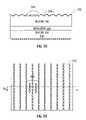
- FIG. 4Aillustrates a cross-sectional view of an exemplary integrated circuit having lateral sides with a varying profile consistent with some embodiments of the present invention.
- FIG. 4Billustrates a top-down view of an exemplary integrated circuit having lateral sides with a varying profile consistent with some embodiments of the present invention.
- FIG. 5Aillustrates a cross-sectional view of an exemplary integrated circuit including a semiconductor substrate having a backside with a non-uniformly varying profile consistent with some embodiments of the present invention.
- FIG. 5Billustrates a top-down view of an exemplary integrated circuit including a semiconductor substrate having a backside with a non-uniformly varying profile consistent with some embodiments of the present invention.
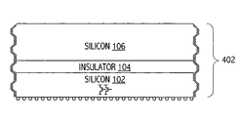
- an exemplary integrated circuit and cooling techniqueincludes a silicon substrate 106 , insulator layer 104 , and silicon layer 102 .
- Silicon layer 102includes substantially all of the circuit devices in packaged integrated circuit 100 .
- the interfacee.g., interface 101 , between silicon layer 102 and conductive bumps 103 is the front side of the integrated circuit.
- Interface 105i.e., the interface between silicon substrate 106 and thermal interface material (TIM) 108 , is the backside of the integrated circuit and is substantially planar.
- Thermal interface material 108is included between metal lid 110 and silicon substrate 106 to eliminate air gaps produced by surface irregularities of metal lid 110 and silicon substrate 106 and to increase joint conductivity to improve heat transfer between metal lid 110 and silicon substrate 106 .
- Thermal interface material 108may be a thermal grease, thermally conductive compound (e.g., an aluminum compound), thermally conductive elastomer, thermally conductive adhesive tape, or other suitable material.
- Heat sink 112(e.g., a fan or other power dissipating structure) is attached to metal lid 110 to increase the heat transfer between metal lid 110 and the ambient environment (e.g., surrounding air).
- An additional thermal interface material layermay be included between metal lid 110 and heat sink 112 to eliminate air gaps between metal lid 110 and heat sink 112 and to increase joint conductivity to improve heat transfer from metal lid 110 to heat sink 112 .
- An exemplary TIMtransfers less heat from the silicon interface than other low-thermal resistance materials (e.g., metals).
- a technique for increasing the heat transfer of the cooling scheme illustrated in FIG. 1includes inserting a layer of material having a high thermal conductivity (i.e., greater than approximately 10 W/mK) between silicon substrate 106 and TIM 108 .
- the rate of heat transfer by this cooling techniquemay be limited by the surface area of the substantially planar interface 105 .
- Interface 105is fixed to the size of the integrated circuit backside, limiting the rate of power dissipation.
- approximately 90% of heat transferred from the integrated circuitis transferred in a positive z-direction (i.e., vertically, in a direction orthogonal to interface 105 ) and approximately 10% of heat transferred from the integrated circuit is transferred in a negative z-direction.
- a negligible amount of heat(typically no more than approximately 1 to 2%) is transferred in a lateral direction (i.e., a direction parallel to interface 105 ) from the lateral sides of the integrated circuit.
- FIGS. 2A–5BTechniques for improving the heat transfer of the aforementioned cooling techniques are illustrated in FIGS. 2A–5B .
- an integrated circuit formed by silicon substrate 106 , insulator layer 104 , and silicon layer 102has at least a portion of its backside (i.e., interface 205 ) that has a varying profile (i.e., a substantially non-planar profile).
- backside processingmay be performed after completion of the front side processing.
- Interface 205may be formed by any suitable manufacturing technique (e.g., patterning and etching the backside of silicon substrate 106 ) to form trenches (e.g., trenches 204 ), vias, holes, grooves, or other suitable non-planar structures in silicon substrate 106 .
- trenchese.g., trenches 204
- viase.g., holes, grooves, or other suitable non-planar structures
- roughing-up the backside of silicon substrate 106forms scratches in the backside of silicon substrate 106 .
- the varying profileincreases the surface area of at least a portion of the interface between silicon substrate 106 and thermally conductive layer 205 , thus increasing the vertical heat transfer from the backside of silicon substrate 106 to an adjacent material.
- Thermally conductive layer 202may be formed on the substantially nonplanar backside of silicon substrate 106 .
- Thermally conductive layer 202may be a metal, diamond, or other suitable thermally conductive material.
- thermally conductive layer 202may be a TIM (e.g., a TIM having a high thermal conductivity), and a separate thermally conductive layer may be excluded.
- the thickness of thermally conductive layer 202may vary with the depth of the trenches and the material used. For example, although a thinner thermally conductive layer may be preferable to a thicker thermally conductive layer, the thermally conductive layer is typically thick enough to provide substantially complete coverage of the trench or other non-planar structure.
- the thermally conductive layermay be too thin, it may be brittle, increasing the likelihood of fracturing the thermally conductive layer, which may impede lateral heat transfer across the layer.
- other materialse.g., silver, gold, diamond, etc.
- coppermay be used because it is softer and less expensive than other thermal conductors.
- diamondis a better thermal conductor than other materials (e.g., materials including copper, silver, or gold), in general, to form a diamond layer on the integrated circuit, the integrated circuit is typically exposed to hot conditions and high pressure, which may be undesirable in some applications.
- forming thicknesses of a diamond layer greater than approximately 1000 ⁇ mmay be too time consuming for some applications.
- the depth of the profile of the backside of silicon substrate 106may depend on the material chosen to be the thermal conductor. For example, when using diamond as the thermal conductor, since diamond is also an electrical insulator, the profile depth may extend through the silicon substrate to insulator layer 104 . However, the profile depth may extend through less than the entire silicon substrate to reduce the likelihood of electrical coupling to circuitry in silicon layer 102 , e.g., when an electrically conductive material is chosen as the thermal conductor.
- the integrated circuit of FIG. 2Ais packaged in a lidless package, transferring heat from the backside of silicon substrate 102 to the ambient environment via a substantially non-planar interface between thermally conductive layer 202 and the ambient environment.
- a thermally conductive layere.g., thermally conductive layer 302 of FIG. 3
- thermally conductive layer 302may be a TIM (e.g., a TIM having a high thermal conductivity), and a separate thermally conductive layer may be excluded.
- One technique for improving the vertical heat transferincludes thinning the integrated circuit die, which may make thermal dissipation in the lateral direction more critical.
- the lateral heat transfer of an integrated circuitmay be increased by increasing the surface area of the lateral sides of the integrated circuit as illustrated in FIGS. 4A and 4B .
- Conventional techniques to form a varying profilemay be used to vary the profile of a portion of a lateral side of an integrated circuit, prior to the integrated circuits being separated from a wafer into individual die.
- Conventional techniques for forming a varying profile on the front side or backside of an integrated circuitmay be adapted to form a varying profile on a lateral side of the integrated circuit (e.g., using specialized chambers) after the integrated circuit die has been separated from the wafer.
- a laser or other suitable techniquemay also be used to vary the profile of the lateral sides of the integrated circuit die.
- thermally conductive layer 402may be formed on the lateral sides.
- thermally conductive layer 402may include copper, silver, gold, diamond, a TIM, or other suitable thermally conductive materials.
- the depth of thermally conductive layer 402may be chosen according to the material chosen for the layer, as described above, and according to the location of devices in silicon layer 102 .
- the profile of the silicon substrate backside or lateral sidesmay be tailored according to a heat profile of the integrated circuit design. For example, some portions of the integrated circuit (i.e., hot spots, e.g., those portions exercised at a high rate) may generate more heat than others. Hot spots may slow down transistors proximate to the hot spots and contribute to race conditions in the integrated circuit. Regions of a lateral side or backside having greater profile variations than other locations of the integrated circuit (e.g., trenches 502 ) may be included to improve thermal power dissipation of these hot spots, as illustrated in FIGS. 5A and 5B . Thus, this technique may reduce the occurrence of hot spots and race conditions produced by those hot spots.
- the varying profilemay also be configured in patterns that strengthen the integrated circuit die as compared to other profiles (e.g., cross-hatching or serpentine patterns).
Landscapes
- Engineering & Computer Science (AREA)
- Chemical & Material Sciences (AREA)
- Materials Engineering (AREA)
- Physics & Mathematics (AREA)
- Condensed Matter Physics & Semiconductors (AREA)
- General Physics & Mathematics (AREA)
- Computer Hardware Design (AREA)
- Microelectronics & Electronic Packaging (AREA)
- Power Engineering (AREA)
- Cooling Or The Like Of Semiconductors Or Solid State Devices (AREA)
- Bipolar Transistors (AREA)
- Internal Circuitry In Semiconductor Integrated Circuit Devices (AREA)
Abstract
Description
Claims (18)
Priority Applications (3)
| Application Number | Priority Date | Filing Date | Title |
|---|---|---|---|
| US11/050,572US7259458B2 (en) | 2004-08-18 | 2005-02-03 | Integrated circuit with increased heat transfer |
| PCT/US2005/015048WO2006022911A1 (en) | 2004-08-18 | 2005-04-29 | Integrated circuit with increased heat transfer |
| TW094126485ATWI416675B (en) | 2004-08-18 | 2005-08-04 | Integrated circuit with increased heat conduction |
Applications Claiming Priority (2)
| Application Number | Priority Date | Filing Date | Title |
|---|---|---|---|
| US92076404A | 2004-08-18 | 2004-08-18 | |
| US11/050,572US7259458B2 (en) | 2004-08-18 | 2005-02-03 | Integrated circuit with increased heat transfer |
Related Parent Applications (1)
| Application Number | Title | Priority Date | Filing Date |
|---|---|---|---|
| US92076404AContinuation-In-Part | 2004-08-18 | 2004-08-18 |
Publications (2)
| Publication Number | Publication Date |
|---|---|
| US20060038283A1 US20060038283A1 (en) | 2006-02-23 |
| US7259458B2true US7259458B2 (en) | 2007-08-21 |
Family
ID=35502696
Family Applications (1)
| Application Number | Title | Priority Date | Filing Date |
|---|---|---|---|
| US11/050,572Expired - LifetimeUS7259458B2 (en) | 2004-08-18 | 2005-02-03 | Integrated circuit with increased heat transfer |
Country Status (3)
| Country | Link |
|---|---|
| US (1) | US7259458B2 (en) |
| TW (1) | TWI416675B (en) |
| WO (1) | WO2006022911A1 (en) |
Cited By (2)
| Publication number | Priority date | Publication date | Assignee | Title |
|---|---|---|---|---|
| US20090242257A1 (en)* | 2008-03-31 | 2009-10-01 | Tdk Corporation | Electronic component and electronic component module |
| US20100151678A1 (en)* | 2008-12-15 | 2010-06-17 | Mark Dydyk | Wafer Backside Grinding with Stress Relief |
Families Citing this family (7)
| Publication number | Priority date | Publication date | Assignee | Title |
|---|---|---|---|---|
| KR100883807B1 (en)* | 2007-05-21 | 2009-02-17 | 삼성전자주식회사 | Semiconductor device package and manufacturing method thereof |
| JP4345855B2 (en)* | 2007-07-31 | 2009-10-14 | セイコーエプソン株式会社 | Semiconductor device, heat radiator, and method for manufacturing semiconductor device |
| US8283776B2 (en) | 2010-01-26 | 2012-10-09 | Qualcomm Incorporated | Microfabricated pillar fins for thermal management |
| US8624404B1 (en) | 2012-06-25 | 2014-01-07 | Advanced Micro Devices, Inc. | Integrated circuit package having offset vias |
| KR20140009731A (en)* | 2012-07-12 | 2014-01-23 | 삼성전자주식회사 | Semiconductor chip comprising heat radiation part and method for fabricating the same chip |
| AU2013364020B2 (en) | 2012-12-22 | 2018-01-18 | Gas Technologies Llc | Method and apparatus for providing oxygenated hydrocarbons |
| FR3061600B1 (en)* | 2017-01-03 | 2020-06-26 | Stmicroelectronics (Grenoble 2) Sas | ELECTRONIC DEVICE COMPRISING A GROOVED CHIP |
Citations (23)
| Publication number | Priority date | Publication date | Assignee | Title |
|---|---|---|---|---|
| US5196785A (en) | 1990-12-12 | 1993-03-23 | Hewlett-Packard Company | Tape automated bonding test apparatus for thermal, mechanical and electrical coupling |
| US5206713A (en)* | 1990-06-29 | 1993-04-27 | Digital Equipment Corporation | Mounting silicon chips |
| US5223747A (en) | 1990-06-15 | 1993-06-29 | Battelle-Institut E.V. | Heat dissipating device |
| US5767578A (en) | 1994-10-12 | 1998-06-16 | Siliconix Incorporated | Surface mount and flip chip technology with diamond film passivation for total integated circuit isolation |
| US5773362A (en) | 1996-06-20 | 1998-06-30 | International Business Machines Corporation | Method of manufacturing an integrated ULSI heatsink |
| US5990552A (en) | 1997-02-07 | 1999-11-23 | Intel Corporation | Apparatus for attaching a heat sink to the back side of a flip chip package |
| US6100199A (en) | 1998-01-13 | 2000-08-08 | International Business Machines Corporation | Embedded thermal conductors for semiconductor chips |
| US6184064B1 (en)* | 2000-01-12 | 2001-02-06 | Micron Technology, Inc. | Semiconductor die back side surface and method of fabrication |
| US6225695B1 (en) | 1997-06-05 | 2001-05-01 | Lsi Logic Corporation | Grooved semiconductor die for flip-chip heat sink attachment |
| US6263566B1 (en) | 1999-05-03 | 2001-07-24 | Micron Technology, Inc. | Flexible semiconductor interconnect fabricated by backslide thinning |
| US6281029B1 (en) | 1999-09-30 | 2001-08-28 | Advanced Micro Devices, Inc. | Probe points for heat dissipation during testing of flip chip IC |
| US6287940B1 (en) | 1999-08-02 | 2001-09-11 | Honeywell International Inc. | Dual wafer attachment process |
| US6300670B1 (en) | 1999-07-26 | 2001-10-09 | Stmicroelectronics, Inc. | Backside bus vias |
| US6333557B1 (en) | 2000-09-12 | 2001-12-25 | International Business Machines Corporation | Semiconductor chip structures with embedded thermal conductors |
| DE10030443A1 (en) | 2000-06-22 | 2002-01-17 | Infineon Technologies Ag | Production of a heat deviating surface of a component used in the production of a semiconductor element comprises inserting trenches into the component using an etching process |
| US6512292B1 (en) | 2000-09-12 | 2003-01-28 | International Business Machines Corporation | Semiconductor chip structures with embedded thermal conductors and a thermal sink disposed over opposing substrate surfaces |
| US6586279B1 (en)* | 2000-11-17 | 2003-07-01 | Sun Microsystems, Inc. | Method of integrating a heat spreader and a semiconductor, and package formed thereby |
| US6607928B1 (en) | 1997-12-30 | 2003-08-19 | Intel Corporation | Integrated circuit device having an embedded heat slug |
| US6613602B2 (en) | 2001-12-13 | 2003-09-02 | International Business Machines Corporation | Method and system for forming a thermoelement for a thermoelectric cooler |
| US6627978B2 (en) | 2001-09-28 | 2003-09-30 | Intel Corporation | Chip package enabling increased input/output density |
| US6710442B1 (en)* | 2002-08-27 | 2004-03-23 | Micron Technology, Inc. | Microelectronic devices with improved heat dissipation and methods for cooling microelectronic devices |
| US20040061163A1 (en) | 2002-09-18 | 2004-04-01 | Yoshiaki Nakayama | Semiconductor equipment |
| US6774482B2 (en)* | 2002-12-27 | 2004-08-10 | International Business Machines Corporation | Chip cooling |
- 2005
- 2005-02-03USUS11/050,572patent/US7259458B2/ennot_activeExpired - Lifetime
- 2005-04-29WOPCT/US2005/015048patent/WO2006022911A1/enactiveApplication Filing
- 2005-08-04TWTW094126485Apatent/TWI416675B/ennot_activeIP Right Cessation
Patent Citations (23)
| Publication number | Priority date | Publication date | Assignee | Title |
|---|---|---|---|---|
| US5223747A (en) | 1990-06-15 | 1993-06-29 | Battelle-Institut E.V. | Heat dissipating device |
| US5206713A (en)* | 1990-06-29 | 1993-04-27 | Digital Equipment Corporation | Mounting silicon chips |
| US5196785A (en) | 1990-12-12 | 1993-03-23 | Hewlett-Packard Company | Tape automated bonding test apparatus for thermal, mechanical and electrical coupling |
| US5767578A (en) | 1994-10-12 | 1998-06-16 | Siliconix Incorporated | Surface mount and flip chip technology with diamond film passivation for total integated circuit isolation |
| US5773362A (en) | 1996-06-20 | 1998-06-30 | International Business Machines Corporation | Method of manufacturing an integrated ULSI heatsink |
| US5990552A (en) | 1997-02-07 | 1999-11-23 | Intel Corporation | Apparatus for attaching a heat sink to the back side of a flip chip package |
| US6225695B1 (en) | 1997-06-05 | 2001-05-01 | Lsi Logic Corporation | Grooved semiconductor die for flip-chip heat sink attachment |
| US6607928B1 (en) | 1997-12-30 | 2003-08-19 | Intel Corporation | Integrated circuit device having an embedded heat slug |
| US6100199A (en) | 1998-01-13 | 2000-08-08 | International Business Machines Corporation | Embedded thermal conductors for semiconductor chips |
| US6263566B1 (en) | 1999-05-03 | 2001-07-24 | Micron Technology, Inc. | Flexible semiconductor interconnect fabricated by backslide thinning |
| US6300670B1 (en) | 1999-07-26 | 2001-10-09 | Stmicroelectronics, Inc. | Backside bus vias |
| US6287940B1 (en) | 1999-08-02 | 2001-09-11 | Honeywell International Inc. | Dual wafer attachment process |
| US6281029B1 (en) | 1999-09-30 | 2001-08-28 | Advanced Micro Devices, Inc. | Probe points for heat dissipation during testing of flip chip IC |
| US6184064B1 (en)* | 2000-01-12 | 2001-02-06 | Micron Technology, Inc. | Semiconductor die back side surface and method of fabrication |
| DE10030443A1 (en) | 2000-06-22 | 2002-01-17 | Infineon Technologies Ag | Production of a heat deviating surface of a component used in the production of a semiconductor element comprises inserting trenches into the component using an etching process |
| US6333557B1 (en) | 2000-09-12 | 2001-12-25 | International Business Machines Corporation | Semiconductor chip structures with embedded thermal conductors |
| US6512292B1 (en) | 2000-09-12 | 2003-01-28 | International Business Machines Corporation | Semiconductor chip structures with embedded thermal conductors and a thermal sink disposed over opposing substrate surfaces |
| US6586279B1 (en)* | 2000-11-17 | 2003-07-01 | Sun Microsystems, Inc. | Method of integrating a heat spreader and a semiconductor, and package formed thereby |
| US6627978B2 (en) | 2001-09-28 | 2003-09-30 | Intel Corporation | Chip package enabling increased input/output density |
| US6613602B2 (en) | 2001-12-13 | 2003-09-02 | International Business Machines Corporation | Method and system for forming a thermoelement for a thermoelectric cooler |
| US6710442B1 (en)* | 2002-08-27 | 2004-03-23 | Micron Technology, Inc. | Microelectronic devices with improved heat dissipation and methods for cooling microelectronic devices |
| US20040061163A1 (en) | 2002-09-18 | 2004-04-01 | Yoshiaki Nakayama | Semiconductor equipment |
| US6774482B2 (en)* | 2002-12-27 | 2004-08-10 | International Business Machines Corporation | Chip cooling |
Non-Patent Citations (3)
| Title |
|---|
| AMD, "Thermal, Mechanical, and Chassis Cooling Design Guide," Advanced Micro Devices, Inc., Publication #23794, Rev. H, Nov. 2002, pp. i-x and 1-20. |
| deSorgo, Dr. Miksa, "Thermal Interface Materials," Electronics Cooling, http://www.electronics-cooling.com/Resources/EC<SUB>-</SUB>Articles/SEP96/sep96<SUB>-</SUB>01.htm, Sep. 1996, pp. 1-7. |
| PCT International Search Report PCT/US2005/015048, mailed Jan. 26, 2006; Applicant: Advanced Micro Devices, Inc.; International Filing Date, Apr. 29, 2005; 12 pages. |
Cited By (4)
| Publication number | Priority date | Publication date | Assignee | Title |
|---|---|---|---|---|
| US20090242257A1 (en)* | 2008-03-31 | 2009-10-01 | Tdk Corporation | Electronic component and electronic component module |
| US8294036B2 (en)* | 2008-03-31 | 2012-10-23 | Tdk Corporation | Electronic component and electronic component module |
| US20100151678A1 (en)* | 2008-12-15 | 2010-06-17 | Mark Dydyk | Wafer Backside Grinding with Stress Relief |
| US8222118B2 (en)* | 2008-12-15 | 2012-07-17 | Intel Corporation | Wafer backside grinding with stress relief |
Also Published As
| Publication number | Publication date |
|---|---|
| WO2006022911A1 (en) | 2006-03-02 |
| US20060038283A1 (en) | 2006-02-23 |
| TWI416675B (en) | 2013-11-21 |
| TW200616183A (en) | 2006-05-16 |
Similar Documents
| Publication | Publication Date | Title |
|---|---|---|
| CN112534574B (en) | Large metal pads on top of TSVs | |
| CN112470270B (en) | Offset pads on TSV | |
| US7492041B2 (en) | Diamond-silicon hybrid integrated heat spreader | |
| US6519154B1 (en) | Thermal bus design to cool a microelectronic die | |
| US20100019385A1 (en) | Implementing Reduced Hot-Spot Thermal Effects for SOI Circuits | |
| US12230550B2 (en) | Structures and methods for heat dissipation of semiconductor devices | |
| US20090174050A1 (en) | In-plane silicon heat spreader and method therefor | |
| CN101292348A (en) | Stackable wafer or die package with enhanced thermal and device performance | |
| US7842553B2 (en) | Cooling micro-channels | |
| US7259458B2 (en) | Integrated circuit with increased heat transfer | |
| CN110098153A (en) | Electric power electronic module and the method for manufacturing electric power electronic module | |
| CN100550360C (en) | Equipment and system and manufacture method thereof with bottom heat radiation | |
| US11462457B2 (en) | Using a thermoelectric cooler to reduce heat transfer between heat-conducting plates | |
| CN100385652C (en) | Semiconductor device with a plurality of semiconductor chips | |
| JP2002289750A (en) | Multi-chip module and its radiation structure | |
| CN101437355A (en) | Circuit board and method for manufacturing the same | |
| US20090294955A1 (en) | Cooling device with a preformed compliant interface | |
| US20240282658A1 (en) | Integrated circuit dies with thermally conducting solder perimeter | |
| JP5092274B2 (en) | Semiconductor device | |
| CN107112329A (en) | The semiconductor on insulator of variable topological structure is answered with dorsal part | |
| US7545034B2 (en) | Thermal energy removal structure and method | |
| CN110571206B (en) | Semiconductor structure and forming method thereof and forming method of chip | |
| JP2000031487A (en) | Semiconductor device and manufacturing method thereof | |
| US20240347497A1 (en) | Thermal solutions for advanced semiconductors | |
| JP2001274274A (en) | Semiconductor device |
Legal Events
| Date | Code | Title | Description |
|---|---|---|---|
| AS | Assignment | Owner name:ADVANCED MICRO DEVICES, INC., CALIFORNIA Free format text:ASSIGNMENT OF ASSIGNORS INTEREST;ASSIGNORS:SU, MICHAEL ZHUOYING;EPPES, DAVID H.;REEL/FRAME:016259/0260;SIGNING DATES FROM 20050202 TO 20050203 | |
| FEPP | Fee payment procedure | Free format text:PAYOR NUMBER ASSIGNED (ORIGINAL EVENT CODE: ASPN); ENTITY STATUS OF PATENT OWNER: LARGE ENTITY | |
| STCF | Information on status: patent grant | Free format text:PATENTED CASE | |
| CC | Certificate of correction | ||
| AS | Assignment | Owner name:GLOBALFOUNDRIES INC., CAYMAN ISLANDS Free format text:AFFIRMATION OF PATENT ASSIGNMENT;ASSIGNOR:ADVANCED MICRO DEVICES, INC.;REEL/FRAME:023119/0083 Effective date:20090630 | |
| FPAY | Fee payment | Year of fee payment:4 | |
| FPAY | Fee payment | Year of fee payment:8 | |
| MAFP | Maintenance fee payment | Free format text:PAYMENT OF MAINTENANCE FEE, 12TH YEAR, LARGE ENTITY (ORIGINAL EVENT CODE: M1553); ENTITY STATUS OF PATENT OWNER: LARGE ENTITY Year of fee payment:12 | |
| AS | Assignment | Owner name:GLOBALFOUNDRIES U.S. INC., CALIFORNIA Free format text:ASSIGNMENT OF ASSIGNORS INTEREST;ASSIGNOR:GLOBALFOUNDRIES INC.;REEL/FRAME:054633/0001 Effective date:20201022 | |
| AS | Assignment | Owner name:GLOBALFOUNDRIES U.S. INC., NEW YORK Free format text:RELEASE BY SECURED PARTY;ASSIGNOR:WILMINGTON TRUST, NATIONAL ASSOCIATION;REEL/FRAME:056987/0001 Effective date:20201117 |