US7256589B2 - Capacitive sensor system with improved capacitance measuring sensitivity - Google Patents
Capacitive sensor system with improved capacitance measuring sensitivityDownload PDFInfo
- Publication number
- US7256589B2 US7256589B2US10/134,042US13404202AUS7256589B2US 7256589 B2US7256589 B2US 7256589B2US 13404202 AUS13404202 AUS 13404202AUS 7256589 B2US7256589 B2US 7256589B2
- Authority
- US
- United States
- Prior art keywords
- sensor
- electrodes
- electrode
- capacitance
- shield
- Prior art date
- Legal status (The legal status is an assumption and is not a legal conclusion. Google has not performed a legal analysis and makes no representation as to the accuracy of the status listed.)
- Expired - Fee Related
Links
Images


Classifications
- G—PHYSICS
- G01—MEASURING; TESTING
- G01L—MEASURING FORCE, STRESS, TORQUE, WORK, MECHANICAL POWER, MECHANICAL EFFICIENCY, OR FLUID PRESSURE
- G01L1/00—Measuring force or stress, in general
- G01L1/14—Measuring force or stress, in general by measuring variations in capacitance or inductance of electrical elements, e.g. by measuring variations of frequency of electrical oscillators
- G01L1/142—Measuring force or stress, in general by measuring variations in capacitance or inductance of electrical elements, e.g. by measuring variations of frequency of electrical oscillators using capacitors
- G01L1/146—Measuring force or stress, in general by measuring variations in capacitance or inductance of electrical elements, e.g. by measuring variations of frequency of electrical oscillators using capacitors for measuring force distributions, e.g. using force arrays
- G—PHYSICS
- G06—COMPUTING OR CALCULATING; COUNTING
- G06V—IMAGE OR VIDEO RECOGNITION OR UNDERSTANDING
- G06V40/00—Recognition of biometric, human-related or animal-related patterns in image or video data
- G06V40/10—Human or animal bodies, e.g. vehicle occupants or pedestrians; Body parts, e.g. hands
- G06V40/12—Fingerprints or palmprints
- G06V40/13—Sensors therefor
- G06V40/1306—Sensors therefor non-optical, e.g. ultrasonic or capacitive sensing
Definitions
- the present inventionrelates generally to capacitive sensor devices, systems, and methods; and more particularly to improved capacitance sensor devices, systems, and methods as are suitable to be fabricated with integrated circuit technology for use in sensing arrays that measure the position of fingerprint artifacts or other electrically conductive structures near the sensor surface.
- the performance of capacitance based sensing or capacitive sensorshave been limited.
- the capacitance between a target electrode and a sense electrodevaries inversely proportional to the relative distance between them, inversely proportional to the relative distance between them squared, or some functional dependence between inverse and inverse quadratic.
- the maximum distance at which a capacitance sensor system can detect target conductors in the vicinity of its sensor areais dependent on the minimum capacitance the system can resolve. If the capacitance of the sensor electrode relative to its ambient environment, its reference capacitance, is large compared to the capacitance between the target electrode and the sensor electrode, the capacitance sensor system sensitivity is significantly degraded.
- the sensor electrodehas significant reference capacitance alone.
- the size of the sensor electrodeis dictated by the size of fingerprint artifacts, which is typically about the size of a 100 micrometer square. Being part of an integrated circuit whose vertical dimensions are small compared to 100 micrometers, the sensor electrode itself has significant capacitance to the substrate on which it physically or mechanically rests.
- a sensor arraycomposed of a rectangular grid of sensor electrodes was disclosed by Knapp in U.S. Pat. No. 5,325,442.
- Each sense electrodeis connected through a passive switch to array wiring that is the length of the array.
- the array wireis connected to a charge sensing circuit to determine the capacitance.
- the capacitance sensitivityis degraded by the array wiring as the effective reference capacitance on each sensor electrode increased.
- semiconductor switchesare introduced into the sensor area where they may be damaged by mechanical contact with the target electrode, or may leak due to photocurrent in the sensor is operated in a high light level environment. Additional coatings may be applied to the sensor surface to reduce the sensor's susceptibility to damage, but at an increase in the sensor to target electrode distance.
- Ackland et al.disclose a method to reduce the sensor electrode capacitance by introducing a shield electrode between the sensor electrode and the physical support structure at ground potential.
- This reference capacitance cancellation techniqueis applied individually to each sensor electrode, resulting in some reduction in the reference capacitance and a proportional increase in the sensor capacitance sensitivity.
- the amplifier used in the feedback circuitwas a source follower whose gain was significantly less than unity. This resulted in incomplete reference capacitance cancellation, but required no additional circuitry and little additional power.
- the inventionprovides device, system, and method for a capacitive sensor that increases capacitance sensor sensitivity relative to known designs while reducing power consumption and increasing mechanical robustness in use. It also provides a lower cost sensor resulting at least in part from reductions in circuit size and the use of CMOS technology.
- Capacitance measurementutilizes a charge pump circuit, a particular type of switched capacitor, which is well suited to CMOS technology implementation. In the switched capacitor circuit, the sensor electrode is repeatedly charged and discharged to measure its associated capacitance.
- background capacitance cancellationmay be implemented, and when such background capacitance cancellation is used, the shield electrode is repeatedly charged and discharged relative to ground as the shield potential follows the sensor electrode. Background capacitance is also referred to as parasitic or reference level capacitance. To avoid this potential problem and the large transistors required to drive the shield electrode, the shield is segmented such that only the rows or columns of sensor electrodes being measured are experiencing background capacitance cancellation. To further reduce the power, active amplifiers for the cancellation are advantageously replaced with switches.
- the rate at which capacitances can be measuredis increased relative to conventional devices and methods by providing switch capacitance measurement circuitry to all array columns.
- One sensor element along each columnmay be addressed during any measurement period and simultaneous addressing of multiple rows of sensor cells is possible.
- voltages or potentials other than the power supply voltage and ground voltage or potentialmay alternatively be used and provide improved operation, but the cost in terms of power and circuit area may not be justified in some embodiments of the invention.
- the use of full power supply potential swing on the shield electrodesallows for the use of simpler shield electrode design. This full swing improves the capacitance background cancellation such that the array wire capacitances in asymmetrical arrays can be cancelled.
- the inventionprovides a capacitance sensor system including a semiconductor integrated circuit in which no MOS devices are beneath or between any sensor or shield electrodes, a plurality of sensor and shield electrodes, and a plurality of circuits.
- the inventionprovides a capacitance sensor device including: a semiconductor integrated circuit, a plurality of sensor electrodes arranged as an array, a plurality of shield electrodes, a plurality of amplifier circuits, a plurality of charge pump circuits; and a plurality of switches that allows the connection amongst the circuits and the electrodes.
- this capacitive sensor devicehas no MOS devices within the integrated circuit area beneath or between any of the sensor electrodes or shield electrodes.
- the inventionprovides a method of operating the capacitive sensor generally and a methods and procedures for operating component circuits to provide the desired operation and capacitance change, variation, or difference detection sensitivity.
- the inventionprovides an information appliance (such as a computer, personal data assistant, or smart phone) or communication device (such as a mobile telephone) incorporating the inventive sensor for fingerprint sense based access, identification, and/or verification.
- an information appliancesuch as a computer, personal data assistant, or smart phone
- communication devicesuch as a mobile telephone
- FIG. 1illustrates a representative embodiment of a capacitive sensor system, including of physical electrodes and electronic circuits
- FIG. 2is an embodiment of a charge-pump type electronic circuit for determining capacitance between electrical nodes
- FIG. 3is an embodiment of a charge-pump type electronic circuit with improved power efficiency
- FIG. 4is a schematic representation of a portion of an embodiment of a capacitive sensor array using the localized reference capacitance cancellation
- FIG. 5is an embodiment of a portion of a capacitive sensor system using a switch matrix physically external to the sensor area;
- FIG. 6illustrates two switch matrix configurations for the capacitive array sensor of the embodiment illustrated in FIG. 5 ;
- FIG. 7is an embodiment of a portion of the capacitive sensor system using a column-shared reference capacitance cancellation
- FIG. 8illustrates two switch matrix configurations for the capacitive array sensor of the embodiment illustrated in FIG. 7 ;
- FIG. 9is an embodiment of a portion of a capacitive sensor system using array-shared reference capacitance cancellation
- FIG. 10is an embodiment of a portion of a capacitive sensor system using row-shared reference cancellation.
- FIG. 11is an embodiment of a portion of a capacitive sensor system using row-shared reference cancellation and column switch matrixes external to the sensor array.
- the present inventionincreases capacitance sensor sensitivity while reducing power consumption and increasing mechanical robustness in use. Cost reductions result from reductions in circuit size as well as the use of CMOS technology not modified for sensor or fingerprint applications.
- the primary capacitance measurement techniqueis implemented as a charge pump circuit, a particular type of switched capacitor.
- Such circuitsare well suited to CMOS (or other MOS) technology implementation. Unlike active circuits, circuits consume very little static power. However, their dynamic power can be significant if the capacitive loads or the operating frequencies are high.
- the sensor electrodeIn the switch capacitor circuit, the sensor electrode is repeatedly charged and discharged to measure its associated capacitance. If background capacitance cancellation is used, the shield electrode is repeatedly charged and discharged relative to ground as the shield potential follows the sensor electrode. Background capacitance is also referred to as parasitic or reference level capacitance. To avoid this potential problem and the large transistors required to drive the shield electrode, the shield is segmented such that only the rows or columns of sensor electrodes being measured are experiencing background capacitance cancellation. To further reduce the power, active amplifiers for the cancellation are replaced with switches.
- all columnscontain switch capacitance measurement circuitry.
- One sensor element along each columnmay be addressed during any measurement period. Simultaneous addressing of multiple rows of sensor cells is possible.
- FIG. 1shows an elementary part of an embodiment of a capacitive sensor system consisting of a single sense electrode E 1 ( 1 ), a single shield electrode E 4 ( 4 ), a single electronic circuit ( 5 ), and a reference electrode E 3 ( 3 ).
- the reference electrode ( 3 )is shown at the same potential as the target electrode E 2 ( 2 ), but the target electrode ( 2 ) need only be at any static potential relative to the reference electrode in a capacitive sensor.
- the electronic circuit ( 1 )determines the capacitance between terminals ( 6 ) and ( 7 ) while applying an appropriate signal to terminal ( 8 ) and to shield electrode ( 4 ).
- FIG. 1further illustrates the feature of the invention as embodied in an integrated circuit.
- the electrodes(single sense electrode E 1 ( 1 ), reference electrode E 3 ( 3 ), and shield electrode E 4 ( 4 )) are primarily parallel to the integrated circuit surface shown in the X-Y plane.
- Sense electrode ( 1 )is physically separated from the reference electrode ( 3 ) by the shield electrode ( 4 ).
- Shield electrode ( 4 )is located beneath the sense electrode ( 1 ) as well as lateral to or minimally above a plane of the sense electrode ( 1 ), but not so far above sense electrode ( 1 ) as to appreciably decrease the capacitance value k 12 between sense electrode ( 1 ) and the target electrode ( 2 ).
- a sense electrode E 1 ( 1 )is disposed in a layered structure in a first plane that is entirely offset from a second plane in which a reference electrode E 3 ( 3 ) is disposed, and is entirely offset from a third plane in which at least one shield electrode E 4 ( 4 ) is disposed.
- the different planes or layersare disposed in an order relative to the Cartesian coordinate system z-axis in the drawing as follows in order of increasing z-axis coordinate value: reference electrode E 3 ( 3 ), shield electrode E 4 ( 4 ), sensor electrode E 1 ( 1 ), and when present a target electrode E 2 ( 2 ).
- shield electrode E 4 ( 4 )The shielding provided by shield electrode E 4 ( 4 ) is described by the values of the capacitance k 13 between sense electrode E 1 ( 1 ) and reference electrode E 3 ( 3 ). If value k 13 is zero, then the shielding between sense electrode E 1 ( 1 ) and reference electrode E 3 ( 3 ) is ideal. Physical realization of an ideal shield electrode ( 4 ) increases the size of shield electrode ( 4 ) which increases the capacitance value k 34 . The electronic circuit ( 5 ) is required to drive this increased capacitance during operation of the sensor system. In this embodiment, physical realization of a near ideal shield electrode ( 4 ) is not required.
- FIG. 2shows the schematic representation of the elementary physical and circuitry design of the embodiment illustrated and described relative to FIG. 1 .
- the capacitor and capacitance C 14 ( 20 ) of value k 14is measured between sense electrode E 1 ( 1 ) and shield electrode E 4 ( 4 ).
- Capacitors C 34 ( 21 ), C 13 ( 19 ) and C 12 ( 18 ) with respective value k 34 , k 13 , and k 12are illustrated in FIG. 2 .
- Electronic circuit ( 5 )measures the capacitance between nodes 6 and 7 using three switches, S 1 ( 11 ), S 2 ( 12 ), and S 3 ( 13 ); a known capacitance C 3 ( 14 ) of value k 3 , two fixed voltage sources F 1 ( 16 ) and F 2 ( 17 ) of potential v 1 and v 2 ; a potential measuring device V ( 10 ), such as a voltage analog to digital converter; and a non-inverting amplifier A ( 17 ) with voltage gain g.
- node ( 8 )is at a fixed potential ( 7 ).
- This circuitfunctions in a sequence of discrete time intervals to determine the value (k 12 +k 13 +k 14 ) associated with capacitors C 12 ( 18 ), C 13 ( 19 ), and C 14 ( 20 ).
- the first time interval in the measurement sequenceis called the pre-charge interval.
- Switches S 1 ( 11 ) and S 2 ( 12 )are closed and switch S 3 ( 13 ) is open.
- Capacitors ( 18 ), ( 19 ), and ( 20 )are charged to potential v 1 by source ( 16 ).
- capacitor ( 14 )is charged to potential v 2 by source ( 15 ).
- the next intervalcalled the open interval
- all switches S 1 ( 11 ), S 2 ( 12 ), and S 3 ( 13 )are open.
- the next intervalis called the evaluate interval in which switches S 1 ( 11 ) and S 2 ( 12 ) are open and switch S 3 ( 13 ) is closed.
- the charge deposited on capacitors ( 18 ), ( 19 ), and ( 20 )is said to have been “pumped” to capacitor ( 14 ).
- Voltmeter Vmeasures the potential v between nodes ( 7 ) and ( 9 ) across capacitor ( 14 ).
- the capacitance value (k 12 +k 13 +k 14 )is equal to the value k 3 ⁇ ((v 2 /v) ⁇ 1)/(1 ⁇ (v 1 /v)) such that v 1 is not equal to v 2 .
- either of v 1 or v 2is set equal to zero without loss of generality. Setting v 2 equal zero simplifies the following explanation.
- the capacitance value (k 12 +k 13 +k 4 ), defined as equal to ksum,can be determined after the first evaluate interval. However, if capacitance ksum is much less than capacitance k 3 , potential v is nearly equal to zero.
- the measurement sequencemay be continued by returning to the open interval and then entering a new interval called the charge interval. In the charge interval, switch S 1 ( 11 ) is closed which increases the potential at node ( 6 ) to v 1 .
- the measurement sequenceagain enters the open interval followed by the evaluate interval to complete the second pump cycle.
- Voltmeter ( 10 )now indicates a different potential or voltage v. Again the value ksum can be determined from k 3 and voltage v.
- the voltage ration v/v 1equals (ksum)/(ksum+k 3 ).
- the voltage ration v/v 1approximately equals 2 ⁇ (ksum)/(ksum+k 3 ).
- the capacitor C 3 ( 14 )is pumped up by charge deposited in the capacitors C 12 ( 18 ), C 13 ( 19 ), and C 14 ( 20 ) by source F 1 ( 16 ). After some number N of such charge and evaluate cycles of the switches S 1 ( 11 ), S 2 ( 12 ) and S 3 ( 13 ), the voltage ration v/v 1 approximately equals N ⁇ (ksum)/(ksum+k 3 ) for the case v/v 1 less than about 0.2.
- An evaluation of the circuit output v to changes in capacitance value k 12can be made starting from a capacitance k 12 value equal 0.
- This initial caserepresents target electrode E 2 ( 2 ) absent from FIG. 1 .
- the most sensitive operating point for measuring capacitance k 12occurs when both capacitors C 13 ( 19 ) and C 14 ( 20 ) have zero value.
- this solutionis overly restrictive so that this condition is not required.
- the condition that a zero value of net charge flow into node ( 6 ) from capacitors C 13 ( 19 ) and C 14 ( 20 )is sufficient to operate the capacitive sensor system at its most sensitive operating point.
- a non-zero value of capacitance k 13is implemented.
- capacitors C 13 ( 19 ) and C 14 ( 20 ) with amplifier A ( 17 )maintains the net charge flow into node ( 6 ) on a cycle-by-cycle basis. However, to maintain net charge flow into node ( 6 ), the detailed signal at node ( 8 ) is less important than the swing at node ( 8 ) during each measurement cycle.
- FIG. 3shows another embodiment of the invention, specifically the amplifier A ( 17 ) is replaced by switches S 11 ( 22 ) and S 4 ( 23 ); and fixed voltage sources F 1 A ( 24 ) of potential v 1 a and F 4 ( 25 ) of potential v 4 .
- the electronic circuit ( 5 )is further divided into a charge pump circuit ( 26 ) and a switch cancellation circuit ( 27 ).
- Switch S 11 ( 22 )opens and closes synchronously with switch S 1 ( 11 ).
- Switch S 4 ( 23 )opens and closes synchronously with switch S 3 ( 13 ).
- the net charge flow into node ( 6 ) averaged over the entire N measurement cyclescan be set to zero. In this manner, the capacitance sensor system can operate at its most sensitive operating point.
- a further simplification of electronic circuit ( 5 )is made in another embodiment of the invention.
- all the voltage sourcesare set to a value of the prime power of the system, Vcc or the reference potential value, such as 0 volts.
- Vccthe prime power of the system
- Vccthe reference potential value
- these solutionsrequire that k 13 and k 14 be appropriately chose in the physical design, particularly in the design of the shield electrode, so as to insure approximately zero net charge flow into node ( 6 ).
- the presence of electrode E 2 ( 2 )can be detected by measuring the capacitance value k 12 between target electrode E 2 ( 2 ) and sense electrode E 1 ( 1 ).
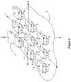
- this embodiment of the inventionadds additional electrodes adjacent to E 1 ( 1 ) in the X-Y plane to form an array. Additional electrodes are desirably added adjacent to shield electrode E 4 ( 4 ) as well as additional electronic circuits ( 5 ).
- At least one sense electrode E 1 ( 1 )is disposed in a layered structure in a first plane that is entirely offset from a second plane in which at least one of an at least one reference electrode E 3 ( 3 ) is disposed, and is entirely offset from a third plane in which a shield electrode E 4 ( 4 ) is disposed.
- the different planes or layersare disposed in an order relative to the Cartesian coordinate system z-axis in the drawing as follows in order of increasing z-axis coordinate value: reference electrode E 3 ( 3 ), a plurality of shield electrodes E 4 ( 4 ), a plurality of sensor electrodes E 1 ( 1 ), and when present a target electrode E 2 ( 2 ).
- an electronic circuit ( 5 )is illustrated for each pair of sense electrode E 1 ( 1 ) and shield electrodes E 4 ( 4 ) in a layer separate from but between the layers of the reference electrode E 3 ( 3 ) and the shield electrodes E 4 ( 4 ).
- array sizes larger than 3 ⁇ 3are used, but these larger arrays use the same principles of operation as a 3 ⁇ 3 array which will illustrate the principles embodied in the invention.
- Only one target electrode E 2 ( 2 ) at an unknown static potentialis illustrated, but more than one electrode can be simultaneously sensed by the described capacitive sensor system.
- an array of electronic circuits ( 5 )is more difficult and required additional circuit area and adds complexity to the entire capacitance sensor system.
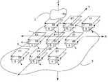
- FIG. 5illustrates the detailed connections required to implement the center two columns of an example of a 4 ⁇ 4 array. For clarity, only two switch matrixes ( 28 ) and ( 29 ) are shown. Because of the deleterious effects of the wire length connecting electrodes ( 1 ) and ( 4 ) to the switches ( 28 ) and circuits ( 5 ), the embodiment is preferential advantageous to X-Y arrays in which the array length in the Y direction is reduced.
- E 21is a sense electrode connected by a wire to the common point between switches S 1 A and S 1 B.
- E 24is a sense electrode connected by a wire to the common point between switches S 4 A and S 4 B.
- Shield electrode E 21 Cis connected by a wire to switch S 1 C and shield electrode E 24 C is connected by a wire to switch S 4 C.
- E 31is a sense electrode connected by a wire to the common point between switches T 1 A and T 1 B.
- E 34is a sense electrode connected by a wire to the common point between switches T 4 A and T 4 B.
- Shield electrode E 31 Cis connected by a wire to switch T 1 C and shield electrode E 34 C is connected by a wire to switch T 4 C.
- one of the sensor electrodes E 21 to E 24is connected to node ( 6 ) of circuit ( 5 ).
- the selected electrodes E 21 to E 24 and/or E 21 C to E 24 Cbecome the shield electrode(s) connected to node ( 8 ).
- capacitance values k 13 and k 14 as seen by electronic circuit ( 5 )can be changed and the capacitance sensor operation improved and desirably optimized.
- the same type of configuration of the T switches ( 29 )allows the third column to select a sense electrode and connect it to node ( 6 ) and-or one or more shield electrodes and connect it (them) to node ( 8 ).
- the switch matrixes ( 28 ) and ( 29 )are electronic, they can be switched rapidly so that the position of many target electrodes E 2 ( 2 ) may be located above the X-Y plane of sense electrode ( 1 ).
- FIG. 6further illustrates specific features of the switch closures ( 30 ) and ( 36 ) used in an embodiment of the invention.
- Sensor electrode E 22 ( 31 )is connected to node ( 6 ).
- Shield electrode E 22 C ( 32 )is connected to node ( 8 ).
- sense electrodes E 21 ( 33 ), E 23 ( 34 ), and E 24 ( 35 )are connected to node ( 8 ) and act as shield electrodes.
- sensor electrode E 33 ( 37 )is connected to node ( 6 ).
- E 33 C ( 39 ), E 34 C ( 40 ), and E 32 C ( 38 )are connected to node ( 8 ). The other sensor electrodes in the column are not connected.
- Switch matrixes ( 42 ) and ( 43 )have two thirds the elements compared as compared to the number in the FIG. 5 and FIG. 6 embodiment. The amount of wiring parallel to each column is reduced by half as compared to the FIG. 5 and FIG. 6 embodiment. For the second column there is only one shield electrode E 2 A ( 44 ), which is connected to node ( 8 ). For the third column there is only one shield electrode E 3 A ( 45 ), which is connected to node ( 8 ).
- FIG. 8illustrates specific switch closures ( 46 ) and ( 48 ) generally described relative to the embodiment in FIG. 7 .
- sensor electrode E 23 ( 47 )is connected to node ( 6 ). All other electrodes in the second column are unconnected.
- sensor electrode E 32 ( 47 )is connected to node ( 6 ).
- E 31 ( 50 ) and E 33 ( 51 )are also connected to ( 8 ) and act as shield electrodes.
- FIGS. 5-8show a common feature of embodiment, specifically that all the switch elements ( 28 ), ( 29 ), ( 30 ), ( 36 ), ( 42 ), ( 43 ), ( 46 ), and ( 48 ) as well as electronic circuits ( 5 ) are physically located outside the sensor electrode array ( 1 ).
- the sensor array areais defined here as the area of the integrated circuit in the X-Y plane that is under in between sensor electrodes ( 1 ).
- Another common feature or embodiment illustrated in FIGS. 5-8is that each column is individually addressed. Sense electrodes ( 1 ) from different rows may be simultaneously addressed. All columns may simultaneously measure one sensor electrode ( 1 ) per row. However, the power required from the electronic circuit ( 5 ) through the wire ( 8 ) to simultaneously drive all shield electrodes as in FIG. 7 and FIG. 8 is significant owing to the close proximity of reference electrode ( 3 ) and shield electrode ( 4 ).
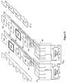
- FIG. 9depicts an embodiment of a configuration in which all shield electrodes ( 53 ) are common and driven by one switch cancellation circuit ( 27 ).
- the capacitance between shield electrode ( 53 ) and reference electrode ( 3 )is approximately 900 picofarads. This capacitance can be reduced significantly by grouping the sense electrodes along rows rather than columns.
- FIG. 10shows an embodiment this alternative structure and method for configuring the shield electrodes ( 54 ) and their respective switch cancellation circuits ( 27 ).
- the shield circuits ( 27 )remain at the edge of the array as in FIGS. 5-8 .
- a reduction in the number of charge pump circuits ( 26 )may be accomplished by adding switches ( 55 ) to each sense electrode ( 21 ).
- the switchesallow for the sense electrodes ( 1 ) to be connected to charge pump circuits ( 26 ) at the edge of the array. Because the wires that connect the switches ( 55 ) are orthogonal to the rows of shield electrodes ( 54 ), the individual capacitances of the sensor electrodes ( 1 ) above the shield electrodes ( 54 ) may be measured simultaneously. Operation of switch cancellation circuits ( 27 ) in adjacent rows improves the shielding, but at the expense of additional power in the switch cancellation circuits ( 27 ).
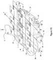
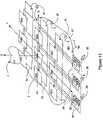
- FIG. 11differs from FIG. 10 only in that the switches ( 55 ) are physically moved outside the sense electrode array area and grouped locally as a switch region ( 56 ).
- wiresare added between the sense electrodes ( 1 ) to carry the signals from the sense electrodes ( 1 ) to the respective switches ( 55 ) devices. Because of the deleterious effects of the wire length connecting electrodes ( 1 ) and to the switches ( 55 ), the embodiment is preferential advantageous to X-Y arrays in which the array length in the Y direction is reduced.
- inventive sensormay be used separately or incorporated into a variety of other devices or systems.
- inventive sensor and sensing methodmay be used with and therefore provides an information appliance (such as a computer, personal data assistant, or smart phone) or communication device (such as a mobile telephone or other information appliance having communication capabilities) incorporating the inventive sensor for fingerprint sense based access, identification, and/or verification.
- an information appliancesuch as a computer, personal data assistant, or smart phone
- communication devicesuch as a mobile telephone or other information appliance having communication capabilities
- the inventionprovides a capacitive sensor based fingerprint swipe sensor integrated or otherwise attached to the surface of a wireless smart communication device.
Landscapes
- Engineering & Computer Science (AREA)
- Physics & Mathematics (AREA)
- General Physics & Mathematics (AREA)
- Human Computer Interaction (AREA)
- Multimedia (AREA)
- Theoretical Computer Science (AREA)
- Power Engineering (AREA)
- Measurement Of Length, Angles, Or The Like Using Electric Or Magnetic Means (AREA)
- Measurement Of The Respiration, Hearing Ability, Form, And Blood Characteristics Of Living Organisms (AREA)
- Image Input (AREA)
Abstract
Description
| U.S. Pat. No. | Date | Inventor(s) | Class |
| 4,210,899 | July 1980 | Swonger, et al. | 340/146.3 E |
| 4,353,056 | October 1982 | Tsikos | 340/146.3 E |
| 4,429,413 | January 1984 | Edwards | 382/4 |
| 4,526,043 | July 1985 | Boie, et al. | 73/862.04 |
| 5,195145 | March 1993 | Backus, et al. | 382/4 |
| 5,325,442 | June 1994 | Knapp | 382/4 |
| 5,434,446 | July 1995 | Hilton, et al. | 257/503 |
| 5,778,089 | July 1998 | Borza | 382/124 |
| 5,828,773 | October 1998 | Setlak, et al. | 382/126 |
| 5,978,496 | November 1999 | Harkin | 382/124 |
| 6,049,620 | April 2000 | Dickinson, et al. | 382/124 |
| 6,055,324 | April 2000 | Fujieda | 382/124 |
| 6,061,464 | May 2000 | Leger | 382/124 |
| 6,097,195 | August 2000 | Ackland, et al. | 324/719 |
| 6,114,862 | September 2000 | Tartagni, et al. | 324/662 |
| 6,289,114 | September 2001 | Mainguet | 324/124 |
| 6,317,508 | November 2001 | Kramer, et al. | 382/124 |
| 6,365,888 | April 2002 | Von Basse, et al. | 250/208.1 |
Claims (42)
Priority Applications (1)
| Application Number | Priority Date | Filing Date | Title |
|---|---|---|---|
| US10/134,042US7256589B2 (en) | 2001-04-27 | 2002-04-25 | Capacitive sensor system with improved capacitance measuring sensitivity |
Applications Claiming Priority (3)
| Application Number | Priority Date | Filing Date | Title |
|---|---|---|---|
| US28723001P | 2001-04-27 | 2001-04-27 | |
| US29285701P | 2001-05-22 | 2001-05-22 | |
| US10/134,042US7256589B2 (en) | 2001-04-27 | 2002-04-25 | Capacitive sensor system with improved capacitance measuring sensitivity |
Publications (2)
| Publication Number | Publication Date |
|---|---|
| US20030016849A1 US20030016849A1 (en) | 2003-01-23 |
| US7256589B2true US7256589B2 (en) | 2007-08-14 |
Family
ID=26964348
Family Applications (1)
| Application Number | Title | Priority Date | Filing Date |
|---|---|---|---|
| US10/134,042Expired - Fee RelatedUS7256589B2 (en) | 2001-04-27 | 2002-04-25 | Capacitive sensor system with improved capacitance measuring sensitivity |
Country Status (6)
| Country | Link |
|---|---|
| US (1) | US7256589B2 (en) |
| EP (1) | EP1390902A4 (en) |
| JP (1) | JP2004534217A (en) |
| AU (1) | AU2002305257A1 (en) |
| TW (1) | TWI242168B (en) |
| WO (1) | WO2002089038A2 (en) |
Cited By (19)
| Publication number | Priority date | Publication date | Assignee | Title |
|---|---|---|---|---|
| US20050163351A1 (en)* | 2002-03-09 | 2005-07-28 | Melfas Co Ltd | Semiconductor fingerprint sensing apparatus with shielding unit |
| US20060270145A1 (en)* | 2005-05-25 | 2006-11-30 | Bach Jerome | Capacitive array |
| US20080129317A1 (en)* | 2006-12-01 | 2008-06-05 | Katsuichi Oba | Input device and method of manufacturing the same |
| US20090216473A1 (en)* | 2004-08-31 | 2009-08-27 | Eaglepicher Technologies, Llc | System and method for nondestructive testing of thermal batteries |
| US20090243632A1 (en)* | 2008-03-27 | 2009-10-01 | Nec Electronics Corporation | Capacitive sensing device and method |
| US20090278655A1 (en)* | 2008-05-06 | 2009-11-12 | The Abraham Joshua Heschel School | Method for inhibiting egress from a chamber containing contaminants |
| US20090327923A1 (en)* | 2008-06-30 | 2009-12-31 | Yahoo! Inc. | Automated system and method for creating a web site based on a subject using information available on the internet |
| US20090327275A1 (en)* | 2008-06-30 | 2009-12-31 | Yahoo! Inc. | Automated system and method for creating a content-rich site based on an emerging subject of internet search |
| US20100039121A1 (en)* | 2008-08-15 | 2010-02-18 | Iliev Simeon K | Low cost fingerprint sensor system |
| US20100082576A1 (en)* | 2008-09-25 | 2010-04-01 | Walker Hubert M | Associating objects in databases by rate-based tagging |
| US20100082575A1 (en)* | 2008-09-25 | 2010-04-01 | Walker Hubert M | Automated tagging of objects in databases |
| US20100156440A1 (en)* | 2005-08-11 | 2010-06-24 | Brose Fahrzeugteile Gmbh & Co. | Anti-Pinch Sensor |
| DE102010023128A1 (en)* | 2010-06-09 | 2011-12-15 | Siemens Aktiengesellschaft | Capacitive sensor |
| US8724038B2 (en) | 2010-10-18 | 2014-05-13 | Qualcomm Mems Technologies, Inc. | Wraparound assembly for combination touch, handwriting and fingerprint sensor |
| US9024910B2 (en) | 2012-04-23 | 2015-05-05 | Qualcomm Mems Technologies, Inc. | Touchscreen with bridged force-sensitive resistors |
| US9158958B2 (en) | 2010-10-28 | 2015-10-13 | Synaptics Incorporated | Signal strength enhancement in a biometric sensor array |
| CN105981040A (en)* | 2014-10-13 | 2016-09-28 | 深圳市汇顶科技股份有限公司 | Sensor pixel circuit for fingerprint recognition |
| US10203816B2 (en) | 2013-05-07 | 2019-02-12 | Egis Technology Inc. | Apparatus and method for TFT fingerprint sensor |
| US11085893B2 (en)* | 2019-09-23 | 2021-08-10 | Whitney Skaling | Capacitive matrix suction sensor having a hydrophilic, non-conductive, porous jacket |
Families Citing this family (43)
| Publication number | Priority date | Publication date | Assignee | Title |
|---|---|---|---|---|
| US6636053B1 (en)* | 2001-11-02 | 2003-10-21 | Stmicroelectronics, Inc. | Capacitive pixel for fingerprint sensor |
| US7085542B2 (en)* | 2002-05-30 | 2006-08-01 | Motorola, Inc. | Portable device including a replaceable cover |
| US7474772B2 (en)* | 2003-06-25 | 2009-01-06 | Atrua Technologies, Inc. | System and method for a miniature user input device |
| US7587072B2 (en)* | 2003-08-22 | 2009-09-08 | Authentec, Inc. | System for and method of generating rotational inputs |
| US7697729B2 (en) | 2004-01-29 | 2010-04-13 | Authentec, Inc. | System for and method of finger initiated actions |
| US20060181521A1 (en)* | 2005-02-14 | 2006-08-17 | Atrua Technologies, Inc. | Systems for dynamically illuminating touch sensors |
| US7831070B1 (en) | 2005-02-18 | 2010-11-09 | Authentec, Inc. | Dynamic finger detection mechanism for a fingerprint sensor |
| US7868874B2 (en) | 2005-11-15 | 2011-01-11 | Synaptics Incorporated | Methods and systems for detecting a position-based attribute of an object using digital codes |
| US7889176B2 (en)* | 2006-07-18 | 2011-02-15 | Avago Technologies General Ip (Singapore) Pte. Ltd. | Capacitive sensing in displacement type pointing devices |
| WO2008017416A2 (en)* | 2006-08-07 | 2008-02-14 | Eth Zurich | Multitransducer array and method for configuring such a device |
| US7584068B2 (en)* | 2007-02-22 | 2009-09-01 | Teradyne, Inc. | Electrically stimulated fingerprint sensor test method |
| KR20100100773A (en)* | 2007-10-04 | 2010-09-15 | 가부시키가이샤후지쿠라 | Capacitive proximity sensor and proximity detection method |
| EP2071312B1 (en)* | 2007-12-13 | 2015-09-16 | Yamaha Corporation | Pressure sensor and data input apparatus |
| KR101237640B1 (en)* | 2008-01-29 | 2013-02-27 | (주)멜파스 | Touchscreen apparatus having structure for preventing forming of parasitic capacitance |
| JP4816668B2 (en)* | 2008-03-28 | 2011-11-16 | ソニー株式会社 | Display device with touch sensor |
| JP2010061405A (en)* | 2008-09-03 | 2010-03-18 | Rohm Co Ltd | Capacitance sensor, detection circuit thereof, input device, and control method of capacity sensor |
| KR101667801B1 (en) | 2009-06-19 | 2016-10-20 | 삼성전자주식회사 | Touch panel and electronic device including the touch panel |
| KR101658991B1 (en)* | 2009-06-19 | 2016-09-22 | 삼성전자주식회사 | Touch panel and electronic device including the touch panel |
| US8258797B2 (en)* | 2009-06-24 | 2012-09-04 | Synaptics Incorporated | Capacitive sensor interference determination |
| KR101616875B1 (en)* | 2010-01-07 | 2016-05-02 | 삼성전자주식회사 | Touch panel and electronic device including the touch panel |
| US8421890B2 (en)* | 2010-01-15 | 2013-04-16 | Picofield Technologies, Inc. | Electronic imager using an impedance sensor grid array and method of making |
| US8791792B2 (en) | 2010-01-15 | 2014-07-29 | Idex Asa | Electronic imager using an impedance sensor grid array mounted on or about a switch and method of making |
| US8866347B2 (en) | 2010-01-15 | 2014-10-21 | Idex Asa | Biometric image sensing |
| KR101631892B1 (en) | 2010-01-28 | 2016-06-21 | 삼성전자주식회사 | Touch panel and electronic device including the touch panel |
| KR101710523B1 (en) | 2010-03-22 | 2017-02-27 | 삼성전자주식회사 | Touch panel and electronic device including the touch panel |
| WO2012027754A2 (en) | 2010-08-27 | 2012-03-01 | Uico, Inc. | Capacitive touch screen having dynamic capacitance control and improved touch-sensing |
| KR101809191B1 (en) | 2010-10-11 | 2018-01-18 | 삼성전자주식회사 | Touch panel |
| KR101735715B1 (en)* | 2010-11-23 | 2017-05-15 | 삼성전자주식회사 | Input sensing circuit and touch panel including the input sensing circuit |
| US8459554B2 (en)* | 2010-11-30 | 2013-06-11 | Stmicroelectronics S.R.L. | Large area monitoring device |
| US9762234B2 (en) | 2011-02-10 | 2017-09-12 | Synaptics Incorporated | Input device interference determination |
| US8847911B2 (en) | 2011-04-05 | 2014-09-30 | Cypress Semiconductor Corporation | Circuit to provide signal to sense array |
| KR101784436B1 (en) | 2011-04-18 | 2017-10-11 | 삼성전자주식회사 | Touch panel and driving device for the touch panel |
| CN102890588B (en)* | 2011-07-21 | 2015-04-08 | 国民技术股份有限公司 | Induction circuit capable of realizing multi-touch location |
| US20130279769A1 (en) | 2012-04-10 | 2013-10-24 | Picofield Technologies Inc. | Biometric Sensing |
| TWI490455B (en)* | 2012-10-12 | 2015-07-01 | Morevalued Technology Co Let | Capacitive sensing array device with high sensitivity and electronic apparatus using the same |
| CN103714330B (en)* | 2014-01-06 | 2017-12-19 | 苏州迈瑞微电子有限公司 | Capacitive fingerprint sensor |
| US9939932B2 (en) | 2014-03-21 | 2018-04-10 | Advanced Sensor Technology Limited | Position sensing device and method using self-capacitance |
| EP2922205B1 (en)* | 2014-03-21 | 2020-12-23 | Melius SA | Position sensing device and method using self-capacitance |
| US9891763B2 (en)* | 2014-09-30 | 2018-02-13 | Synaptics Incorporated | Current feedback techniques for capacitive sensing |
| CN104729769B (en)* | 2015-03-30 | 2017-10-03 | 南京林业大学 | Distributed flexible pressure sensor based on electroactive polymer |
| JPWO2017026446A1 (en)* | 2015-08-10 | 2018-07-05 | 日本電気株式会社 | Wearing body, authentication device, authentication method and program |
| US10395084B2 (en)* | 2017-09-29 | 2019-08-27 | Superc-Touch Corporation | Fingerprint identification device |
| WO2021174543A1 (en)* | 2020-03-06 | 2021-09-10 | 深圳市汇顶科技股份有限公司 | Capacitive detection circuit, touch device, and terminal apparatus |
Citations (90)
| Publication number | Priority date | Publication date | Assignee | Title |
|---|---|---|---|---|
| US4210899A (en) | 1975-06-23 | 1980-07-01 | Fingermatrix, Inc. | Fingerprint-based access control and identification apparatus |
| US4353056A (en) | 1980-06-05 | 1982-10-05 | Siemens Corporation | Capacitive fingerprint sensor |
| US4429413A (en) | 1981-07-30 | 1984-01-31 | Siemens Corporation | Fingerprint sensor |
| US4435056A (en) | 1980-12-26 | 1984-03-06 | Olympus Optical Co., Ltd. | Film feeding device |
| US4526043A (en) | 1983-05-23 | 1985-07-02 | At&T Bell Laboratories | Conformable tactile sensor |
| US4577345A (en) | 1984-04-05 | 1986-03-18 | Igor Abramov | Fingerprint sensor |
| US4785338A (en) | 1979-08-09 | 1988-11-15 | Canon Kabushiki Kaisha | Semi-conductor I.C. element |
| US4860232A (en)* | 1987-04-22 | 1989-08-22 | Massachusetts Institute Of Technology | Digital technique for precise measurement of variable capacitance |
| US5051802A (en) | 1988-01-22 | 1991-09-24 | Thomson-Csf | Compact image sensor |
| US5166679A (en) | 1991-06-06 | 1992-11-24 | The United States Of America As Represented By The Administrator Of The National Aeronautics & Space Administration | Driven shielding capacitive proximity sensor |
| US5195145A (en) | 1989-11-13 | 1993-03-16 | Identity Technologies Incorporated | Apparatus to record epidermal topography |
| US5207102A (en) | 1991-02-12 | 1993-05-04 | Mitsubishi Denki Kabushiki Kaisha | Semiconductor pressure sensor |
| US5214388A (en) | 1992-05-28 | 1993-05-25 | The United States Of America As Represented By The Administrator Of The National Aeronautics And Space Administration | Phase discriminating capacitive array sensor system |
| US5264393A (en) | 1988-11-25 | 1993-11-23 | Fuji Photo Film Co., Ltd. | Solid state image pickup device and method of manufacturing the same |
| US5325442A (en) | 1990-05-18 | 1994-06-28 | U.S. Philips Corporation | Fingerprint sensing device and recognition system having predetermined electrode activation |
| US5373245A (en) | 1993-07-12 | 1994-12-13 | The United States Of America As Represented By The Administrator Of The National Aeronautics And Space Administration | Capaciflector camera |
| US5382310A (en) | 1994-04-29 | 1995-01-17 | Eastman Kodak Company | Packaging medical image sensors |
| US5424249A (en) | 1992-01-23 | 1995-06-13 | Mitsubishi Denki Kabushiki Kaisha | Method of making mold-packaged pressure sensing semiconductor device |
| US5429006A (en) | 1992-04-16 | 1995-07-04 | Enix Corporation | Semiconductor matrix type sensor for very small surface pressure distribution |
| US5434446A (en) | 1993-07-07 | 1995-07-18 | Analog Devices, Inc. | Parasitic capacitance cancellation circuit |
| US5442347A (en) | 1993-01-25 | 1995-08-15 | The United States Of America As Represented By The Administrater, National Aeronautics & Space Administration | Double-driven shield capacitive type proximity sensor |
| US5485011A (en) | 1994-01-28 | 1996-01-16 | Larry C. Y. Lee | Two-sided integrated-circuit PIR sensor package |
| US5539292A (en) | 1994-11-28 | 1996-07-23 | The United States Of America As Represented By The Administrator Of The National Aeronautics And Space Administration | Capaciflector-guided mechanisms |
| US5559961A (en) | 1994-04-04 | 1996-09-24 | Lucent Technologies Inc. | Graphical password |
| US5559504A (en) | 1993-01-08 | 1996-09-24 | Kabushiki Kaisha Toshiba | Surface shape sensor, identification device using this sensor, and protected system using this device |
| US5576763A (en) | 1994-11-22 | 1996-11-19 | Lucent Technologies Inc. | Single-polysilicon CMOS active pixel |
| US5577120A (en) | 1995-05-01 | 1996-11-19 | Lucent Technologies Inc. | Method and apparatus for restrospectively identifying an individual who had engaged in a commercial or retail transaction or the like |
| US5602585A (en) | 1994-12-22 | 1997-02-11 | Lucent Technologies Inc. | Method and system for camera with motion detection |
| US5622873A (en) | 1994-01-24 | 1997-04-22 | Goldstar Electron Co., Ltd. | Process for manufacturing a resin molded image pick-up semiconductor chip having a window |
| US5625304A (en) | 1995-04-21 | 1997-04-29 | Lucent Technologies Inc. | Voltage comparator requiring no compensating offset voltage |
| US5631704A (en) | 1994-10-14 | 1997-05-20 | Lucent Technologies, Inc. | Active pixel sensor and imaging system having differential mode |
| US5668874A (en) | 1995-02-28 | 1997-09-16 | Lucent Technologies Inc. | Identification card verification system and method |
| US5673123A (en) | 1994-06-30 | 1997-09-30 | Lucent Technologies Inc. | Methods and means for processing images |
| US5739562A (en) | 1995-08-01 | 1998-04-14 | Lucent Technologies Inc. | Combined photogate and photodiode active pixel image sensor |
| US5748448A (en) | 1995-02-21 | 1998-05-05 | Nec Corporation | Solid-state image sensor assembly with image sensor element chip mounted in package |
| US5764789A (en) | 1994-11-28 | 1998-06-09 | Smarttouch, Llc | Tokenless biometric ATM access system |
| US5778089A (en) | 1996-03-04 | 1998-07-07 | Dew Engineering And Development Limited | Driver circuit for a contact imaging array |
| US5805422A (en) | 1994-09-21 | 1998-09-08 | Nec Corporation | Semiconductor package with flexible board and method of fabricating the same |
| US5822030A (en) | 1994-09-16 | 1998-10-13 | Seiko Epson Corporation | Liquid crystal display device, its mounting structure and electronic device |
| US5825907A (en) | 1994-12-28 | 1998-10-20 | Lucent Technologies Inc. | Neural network system for classifying fingerprints |
| US5824950A (en) | 1994-03-11 | 1998-10-20 | The Panda Project | Low profile semiconductor die carrier |
| US5828773A (en) | 1996-01-26 | 1998-10-27 | Harris Corporation | Fingerprint sensing method with finger position indication |
| US5844486A (en) | 1997-01-02 | 1998-12-01 | Advanced Safety Concepts, Inc. | Integral capacitive sensor array |
| US5862248A (en) | 1996-01-26 | 1999-01-19 | Harris Corporation | Integrated circuit device having an opening exposing the integrated circuit die and related methods |
| US5864296A (en) | 1997-05-19 | 1999-01-26 | Trw Inc. | Fingerprint detector using ridge resistance sensor |
| US5867368A (en) | 1997-09-09 | 1999-02-02 | Amkor Technology, Inc. | Mounting for a semiconductor integrated circuit device |
| US5869791A (en) | 1995-04-18 | 1999-02-09 | U.S. Philips Corporation | Method and apparatus for a touch sensing device having a thin film insulation layer about the periphery of each sensing element |
| US5901046A (en) | 1996-12-10 | 1999-05-04 | Denso Corporation | Surface mount type package unit and method for manufacturing the same |
| US5903225A (en) | 1997-05-16 | 1999-05-11 | Harris Corporation | Access control system including fingerprint sensor enrollment and associated methods |
| US5920640A (en) | 1997-05-16 | 1999-07-06 | Harris Corporation | Fingerprint sensor and token reader and associated methods |
| EP0929050A2 (en) | 1998-01-13 | 1999-07-14 | STMicroelectronics, Inc. | Scanning capacitive semiconductor fingerprint detector |
| US5940526A (en) | 1997-05-16 | 1999-08-17 | Harris Corporation | Electric field fingerprint sensor having enhanced features and related methods |
| US5963679A (en) | 1996-01-26 | 1999-10-05 | Harris Corporation | Electric field fingerprint sensor apparatus and related methods |
| US5978496A (en) | 1996-04-26 | 1999-11-02 | U.S. Philips Corporation | Fingerprint sensing devices and systems incorporating such |
| US5987156A (en) | 1996-11-25 | 1999-11-16 | Lucent Technologies | Apparatus for correcting fixed column noise in images acquired by a fingerprint sensor |
| US5991408A (en) | 1997-05-16 | 1999-11-23 | Veridicom, Inc. | Identification and security using biometric measurements |
| US6011859A (en) | 1997-07-02 | 2000-01-04 | Stmicroelectronics, Inc. | Solid state fingerprint sensor packaging apparatus and method |
| US6016355A (en) | 1995-12-15 | 2000-01-18 | Veridicom, Inc. | Capacitive fingerprint acquisition sensor |
| US6028773A (en) | 1997-11-14 | 2000-02-22 | Stmicroelectronics, Inc. | Packaging for silicon sensors |
| US6049620A (en) | 1995-12-15 | 2000-04-11 | Veridicom, Inc. | Capacitive fingerprint sensor with adjustable gain |
| US6055324A (en) | 1997-06-30 | 2000-04-25 | Nec Corporation | Fingerprint image entry device of electrostatic capacitance sensing type |
| US6061464A (en) | 1996-11-05 | 2000-05-09 | Thomson-Csf | Fingerprint-reading system with integrated heating resistors |
| US6097195A (en) | 1998-06-02 | 2000-08-01 | Lucent Technologies Inc. | Methods and apparatus for increasing metal density in an integrated circuit while also reducing parasitic capacitance |
| US6114862A (en) | 1996-02-14 | 2000-09-05 | Stmicroelectronics, Inc. | Capacitive distance sensor |
| US6130448A (en) | 1998-08-21 | 2000-10-10 | Gentex Corporation | Optical sensor package and method of making same |
| US6191593B1 (en) | 1997-12-17 | 2001-02-20 | Stmicroelectronics, Inc. | Method for the non-invasive sensing of physical matter on the detection surface of a capacitive sensor |
| US6192142B1 (en) | 1994-11-28 | 2001-02-20 | Smarttouch, Inc. | Tokenless biometric electronic stored value transactions |
| US6195447B1 (en) | 1998-01-16 | 2001-02-27 | Lucent Technologies Inc. | System and method for fingerprint data verification |
| US6208264B1 (en) | 1997-05-23 | 2001-03-27 | Automated Identification Service, Inc. | Personal verification in a commercial transaction system |
| US6211936B1 (en) | 1998-06-16 | 2001-04-03 | Kabushiki Kaisha Toshiba | Liquid crystal display device and method of making the same |
| US6214634B1 (en) | 1997-05-28 | 2001-04-10 | Motorola, Inc. | Sensor device and method of forming a sensor device |
| US6246566B1 (en) | 1999-02-08 | 2001-06-12 | Amkor Technology, Inc. | Electrostatic discharge protection package and method |
| US6259804B1 (en) | 1997-05-16 | 2001-07-10 | Authentic, Inc. | Fingerprint sensor with gain control features and associated methods |
| US6260300B1 (en) | 1999-04-21 | 2001-07-17 | Smith & Wesson Corp. | Biometrically activated lock and enablement system |
| US6268231B1 (en) | 1996-04-08 | 2001-07-31 | Eastman Kodak Company | Low cost CCD packaging |
| US20010017548A1 (en)* | 1998-07-23 | 2001-08-30 | Basse Paul-Werner Von | Method of determining very small capacitances |
| US6289114B1 (en) | 1996-06-14 | 2001-09-11 | Thomson-Csf | Fingerprint-reading system |
| US6320394B1 (en) | 1996-02-14 | 2001-11-20 | Stmicroelectronics S.R.L. | Capacitive distance sensor |
| US6330345B1 (en) | 1997-11-17 | 2001-12-11 | Veridicom, Inc. | Automatic adjustment processing for sensor devices |
| US6342406B1 (en) | 2000-11-15 | 2002-01-29 | Amkor Technology, Inc. | Flip chip on glass image sensor package fabrication method |
| US6362633B1 (en) | 1996-02-14 | 2002-03-26 | Stmicroelectronics S.R.L. | Capacitive distance sensor |
| US6365888B2 (en) | 1998-08-13 | 2002-04-02 | Infineon Technologies Ag | Method for capacitive image acquisition |
| US6396116B1 (en) | 2000-02-25 | 2002-05-28 | Agilent Technologies, Inc. | Integrated circuit packaging for optical sensor devices |
| US6438257B1 (en)* | 1998-07-02 | 2002-08-20 | Nippon Telegraph And Telephone Corporation | Small capacitance change detection device |
| US6483931B2 (en)* | 1997-09-11 | 2002-11-19 | Stmicroelectronics, Inc. | Electrostatic discharge protection of a capacitve type fingerprint sensing array |
| US6501846B1 (en) | 1997-11-25 | 2002-12-31 | Ethentica, Inc. | Method and system for computer access and cursor control using a relief object image generator |
| US6515269B1 (en) | 2000-01-25 | 2003-02-04 | Amkor Technology, Inc. | Integrally connected image sensor packages having a window support in contact with a window and the active area |
| US6518560B1 (en) | 2000-04-27 | 2003-02-11 | Veridicom, Inc. | Automatic gain amplifier for biometric sensor device |
| US6535622B1 (en) | 1999-04-26 | 2003-03-18 | Veridicom, Inc. | Method for imaging fingerprints and concealing latent fingerprints |
| US6546122B1 (en) | 1999-07-29 | 2003-04-08 | Veridicom, Inc. | Method for combining fingerprint templates representing various sensed areas of a fingerprint to derive one fingerprint template representing the fingerprint |
- 2002
- 2002-04-25USUS10/134,042patent/US7256589B2/ennot_activeExpired - Fee Related
- 2002-04-25WOPCT/US2002/013379patent/WO2002089038A2/enactiveApplication Filing
- 2002-04-25EPEP02734067Apatent/EP1390902A4/ennot_activeWithdrawn
- 2002-04-25AUAU2002305257Apatent/AU2002305257A1/ennot_activeAbandoned
- 2002-04-25JPJP2002586262Apatent/JP2004534217A/enactivePending
- 2002-04-29TWTW91108846Apatent/TWI242168B/ennot_activeIP Right Cessation
Patent Citations (100)
| Publication number | Priority date | Publication date | Assignee | Title |
|---|---|---|---|---|
| US4210899A (en) | 1975-06-23 | 1980-07-01 | Fingermatrix, Inc. | Fingerprint-based access control and identification apparatus |
| US4785338A (en) | 1979-08-09 | 1988-11-15 | Canon Kabushiki Kaisha | Semi-conductor I.C. element |
| US4353056A (en) | 1980-06-05 | 1982-10-05 | Siemens Corporation | Capacitive fingerprint sensor |
| US4435056A (en) | 1980-12-26 | 1984-03-06 | Olympus Optical Co., Ltd. | Film feeding device |
| US4429413A (en) | 1981-07-30 | 1984-01-31 | Siemens Corporation | Fingerprint sensor |
| US4526043A (en) | 1983-05-23 | 1985-07-02 | At&T Bell Laboratories | Conformable tactile sensor |
| US4577345A (en) | 1984-04-05 | 1986-03-18 | Igor Abramov | Fingerprint sensor |
| US4860232A (en)* | 1987-04-22 | 1989-08-22 | Massachusetts Institute Of Technology | Digital technique for precise measurement of variable capacitance |
| US5051802A (en) | 1988-01-22 | 1991-09-24 | Thomson-Csf | Compact image sensor |
| US5264393A (en) | 1988-11-25 | 1993-11-23 | Fuji Photo Film Co., Ltd. | Solid state image pickup device and method of manufacturing the same |
| US5195145A (en) | 1989-11-13 | 1993-03-16 | Identity Technologies Incorporated | Apparatus to record epidermal topography |
| US5325442A (en) | 1990-05-18 | 1994-06-28 | U.S. Philips Corporation | Fingerprint sensing device and recognition system having predetermined electrode activation |
| US5207102A (en) | 1991-02-12 | 1993-05-04 | Mitsubishi Denki Kabushiki Kaisha | Semiconductor pressure sensor |
| US5166679A (en) | 1991-06-06 | 1992-11-24 | The United States Of America As Represented By The Administrator Of The National Aeronautics & Space Administration | Driven shielding capacitive proximity sensor |
| US5424249A (en) | 1992-01-23 | 1995-06-13 | Mitsubishi Denki Kabushiki Kaisha | Method of making mold-packaged pressure sensing semiconductor device |
| US5429006A (en) | 1992-04-16 | 1995-07-04 | Enix Corporation | Semiconductor matrix type sensor for very small surface pressure distribution |
| US5214388A (en) | 1992-05-28 | 1993-05-25 | The United States Of America As Represented By The Administrator Of The National Aeronautics And Space Administration | Phase discriminating capacitive array sensor system |
| US5559504A (en) | 1993-01-08 | 1996-09-24 | Kabushiki Kaisha Toshiba | Surface shape sensor, identification device using this sensor, and protected system using this device |
| US5442347A (en) | 1993-01-25 | 1995-08-15 | The United States Of America As Represented By The Administrater, National Aeronautics & Space Administration | Double-driven shield capacitive type proximity sensor |
| US5434446A (en) | 1993-07-07 | 1995-07-18 | Analog Devices, Inc. | Parasitic capacitance cancellation circuit |
| US5373245A (en) | 1993-07-12 | 1994-12-13 | The United States Of America As Represented By The Administrator Of The National Aeronautics And Space Administration | Capaciflector camera |
| US5622873A (en) | 1994-01-24 | 1997-04-22 | Goldstar Electron Co., Ltd. | Process for manufacturing a resin molded image pick-up semiconductor chip having a window |
| US5485011A (en) | 1994-01-28 | 1996-01-16 | Larry C. Y. Lee | Two-sided integrated-circuit PIR sensor package |
| US5824950A (en) | 1994-03-11 | 1998-10-20 | The Panda Project | Low profile semiconductor die carrier |
| US5559961A (en) | 1994-04-04 | 1996-09-24 | Lucent Technologies Inc. | Graphical password |
| US5382310A (en) | 1994-04-29 | 1995-01-17 | Eastman Kodak Company | Packaging medical image sensors |
| US5673123A (en) | 1994-06-30 | 1997-09-30 | Lucent Technologies Inc. | Methods and means for processing images |
| US5822030A (en) | 1994-09-16 | 1998-10-13 | Seiko Epson Corporation | Liquid crystal display device, its mounting structure and electronic device |
| US5805422A (en) | 1994-09-21 | 1998-09-08 | Nec Corporation | Semiconductor package with flexible board and method of fabricating the same |
| US5631704A (en) | 1994-10-14 | 1997-05-20 | Lucent Technologies, Inc. | Active pixel sensor and imaging system having differential mode |
| US5835141A (en) | 1994-11-22 | 1998-11-10 | Lucent Technologies Inc. | Single-polysilicon CMOS active pixel image sensor |
| US5576763A (en) | 1994-11-22 | 1996-11-19 | Lucent Technologies Inc. | Single-polysilicon CMOS active pixel |
| US6192142B1 (en) | 1994-11-28 | 2001-02-20 | Smarttouch, Inc. | Tokenless biometric electronic stored value transactions |
| US5764789A (en) | 1994-11-28 | 1998-06-09 | Smarttouch, Llc | Tokenless biometric ATM access system |
| US5539292A (en) | 1994-11-28 | 1996-07-23 | The United States Of America As Represented By The Administrator Of The National Aeronautics And Space Administration | Capaciflector-guided mechanisms |
| US5602585A (en) | 1994-12-22 | 1997-02-11 | Lucent Technologies Inc. | Method and system for camera with motion detection |
| US5825907A (en) | 1994-12-28 | 1998-10-20 | Lucent Technologies Inc. | Neural network system for classifying fingerprints |
| US5748448A (en) | 1995-02-21 | 1998-05-05 | Nec Corporation | Solid-state image sensor assembly with image sensor element chip mounted in package |
| US5668874A (en) | 1995-02-28 | 1997-09-16 | Lucent Technologies Inc. | Identification card verification system and method |
| US5869791A (en) | 1995-04-18 | 1999-02-09 | U.S. Philips Corporation | Method and apparatus for a touch sensing device having a thin film insulation layer about the periphery of each sensing element |
| US5625304A (en) | 1995-04-21 | 1997-04-29 | Lucent Technologies Inc. | Voltage comparator requiring no compensating offset voltage |
| US5577120A (en) | 1995-05-01 | 1996-11-19 | Lucent Technologies Inc. | Method and apparatus for restrospectively identifying an individual who had engaged in a commercial or retail transaction or the like |
| US5739562A (en) | 1995-08-01 | 1998-04-14 | Lucent Technologies Inc. | Combined photogate and photodiode active pixel image sensor |
| US6049620A (en) | 1995-12-15 | 2000-04-11 | Veridicom, Inc. | Capacitive fingerprint sensor with adjustable gain |
| US6538456B1 (en) | 1995-12-15 | 2003-03-25 | Veridicom, Inc. | Capacitive fingerprint sensor with adjustable gain |
| US6016355A (en) | 1995-12-15 | 2000-01-18 | Veridicom, Inc. | Capacitive fingerprint acquisition sensor |
| US5828773A (en) | 1996-01-26 | 1998-10-27 | Harris Corporation | Fingerprint sensing method with finger position indication |
| US5862248A (en) | 1996-01-26 | 1999-01-19 | Harris Corporation | Integrated circuit device having an opening exposing the integrated circuit die and related methods |
| US5963679A (en) | 1996-01-26 | 1999-10-05 | Harris Corporation | Electric field fingerprint sensor apparatus and related methods |
| US6320394B1 (en) | 1996-02-14 | 2001-11-20 | Stmicroelectronics S.R.L. | Capacitive distance sensor |
| US6496021B2 (en) | 1996-02-14 | 2002-12-17 | Stmicroelectronics, Inc. | Method for making a capacitive distance sensor |
| US6114862A (en) | 1996-02-14 | 2000-09-05 | Stmicroelectronics, Inc. | Capacitive distance sensor |
| US6437583B1 (en) | 1996-02-14 | 2002-08-20 | Stmicroelectronics, Inc.. | Capacitive distance sensor |
| US6362633B1 (en) | 1996-02-14 | 2002-03-26 | Stmicroelectronics S.R.L. | Capacitive distance sensor |
| US20020180464A1 (en) | 1996-02-14 | 2002-12-05 | Stmicroelectronics S.R.L. | Capacitive distance sensor |
| US5778089A (en) | 1996-03-04 | 1998-07-07 | Dew Engineering And Development Limited | Driver circuit for a contact imaging array |
| US6268231B1 (en) | 1996-04-08 | 2001-07-31 | Eastman Kodak Company | Low cost CCD packaging |
| US5978496A (en) | 1996-04-26 | 1999-11-02 | U.S. Philips Corporation | Fingerprint sensing devices and systems incorporating such |
| US6289114B1 (en) | 1996-06-14 | 2001-09-11 | Thomson-Csf | Fingerprint-reading system |
| US6459804B2 (en) | 1996-06-14 | 2002-10-01 | Thomson-Csf | Fingerprint-reading system |
| US6061464A (en) | 1996-11-05 | 2000-05-09 | Thomson-Csf | Fingerprint-reading system with integrated heating resistors |
| US5987156A (en) | 1996-11-25 | 1999-11-16 | Lucent Technologies | Apparatus for correcting fixed column noise in images acquired by a fingerprint sensor |
| US5901046A (en) | 1996-12-10 | 1999-05-04 | Denso Corporation | Surface mount type package unit and method for manufacturing the same |
| US5844486A (en) | 1997-01-02 | 1998-12-01 | Advanced Safety Concepts, Inc. | Integral capacitive sensor array |
| US5920640A (en) | 1997-05-16 | 1999-07-06 | Harris Corporation | Fingerprint sensor and token reader and associated methods |
| US6259804B1 (en) | 1997-05-16 | 2001-07-10 | Authentic, Inc. | Fingerprint sensor with gain control features and associated methods |
| US6069970A (en) | 1997-05-16 | 2000-05-30 | Authentec, Inc. | Fingerprint sensor and token reader and associated methods |
| US5903225A (en) | 1997-05-16 | 1999-05-11 | Harris Corporation | Access control system including fingerprint sensor enrollment and associated methods |
| US5940526A (en) | 1997-05-16 | 1999-08-17 | Harris Corporation | Electric field fingerprint sensor having enhanced features and related methods |
| US5991408A (en) | 1997-05-16 | 1999-11-23 | Veridicom, Inc. | Identification and security using biometric measurements |
| US5864296A (en) | 1997-05-19 | 1999-01-26 | Trw Inc. | Fingerprint detector using ridge resistance sensor |
| US6208264B1 (en) | 1997-05-23 | 2001-03-27 | Automated Identification Service, Inc. | Personal verification in a commercial transaction system |
| US6214634B1 (en) | 1997-05-28 | 2001-04-10 | Motorola, Inc. | Sensor device and method of forming a sensor device |
| US6055324A (en) | 1997-06-30 | 2000-04-25 | Nec Corporation | Fingerprint image entry device of electrostatic capacitance sensing type |
| US6011859A (en) | 1997-07-02 | 2000-01-04 | Stmicroelectronics, Inc. | Solid state fingerprint sensor packaging apparatus and method |
| US5867368A (en) | 1997-09-09 | 1999-02-02 | Amkor Technology, Inc. | Mounting for a semiconductor integrated circuit device |
| US6483931B2 (en)* | 1997-09-11 | 2002-11-19 | Stmicroelectronics, Inc. | Electrostatic discharge protection of a capacitve type fingerprint sensing array |
| US6028773A (en) | 1997-11-14 | 2000-02-22 | Stmicroelectronics, Inc. | Packaging for silicon sensors |
| US6330345B1 (en) | 1997-11-17 | 2001-12-11 | Veridicom, Inc. | Automatic adjustment processing for sensor devices |
| US6501846B1 (en) | 1997-11-25 | 2002-12-31 | Ethentica, Inc. | Method and system for computer access and cursor control using a relief object image generator |
| US6191593B1 (en) | 1997-12-17 | 2001-02-20 | Stmicroelectronics, Inc. | Method for the non-invasive sensing of physical matter on the detection surface of a capacitive sensor |
| US6317508B1 (en) | 1998-01-13 | 2001-11-13 | Stmicroelectronics, Inc. | Scanning capacitive semiconductor fingerprint detector |
| JPH11253428A (en) | 1998-01-13 | 1999-09-21 | St Microelectronics Inc | Scanning capacitive semiconductor fingerprint detector |
| EP0929050A2 (en) | 1998-01-13 | 1999-07-14 | STMicroelectronics, Inc. | Scanning capacitive semiconductor fingerprint detector |
| US6195447B1 (en) | 1998-01-16 | 2001-02-27 | Lucent Technologies Inc. | System and method for fingerprint data verification |
| US6097195A (en) | 1998-06-02 | 2000-08-01 | Lucent Technologies Inc. | Methods and apparatus for increasing metal density in an integrated circuit while also reducing parasitic capacitance |
| US6211936B1 (en) | 1998-06-16 | 2001-04-03 | Kabushiki Kaisha Toshiba | Liquid crystal display device and method of making the same |
| US6438257B1 (en)* | 1998-07-02 | 2002-08-20 | Nippon Telegraph And Telephone Corporation | Small capacitance change detection device |
| US6583632B2 (en) | 1998-07-23 | 2003-06-24 | Micronas Gmbh | Method of determining very small capacitances |
| US20010017548A1 (en)* | 1998-07-23 | 2001-08-30 | Basse Paul-Werner Von | Method of determining very small capacitances |
| US6365888B2 (en) | 1998-08-13 | 2002-04-02 | Infineon Technologies Ag | Method for capacitive image acquisition |
| US6130448A (en) | 1998-08-21 | 2000-10-10 | Gentex Corporation | Optical sensor package and method of making same |
| US6246566B1 (en) | 1999-02-08 | 2001-06-12 | Amkor Technology, Inc. | Electrostatic discharge protection package and method |
| US6260300B1 (en) | 1999-04-21 | 2001-07-17 | Smith & Wesson Corp. | Biometrically activated lock and enablement system |
| US6535622B1 (en) | 1999-04-26 | 2003-03-18 | Veridicom, Inc. | Method for imaging fingerprints and concealing latent fingerprints |
| US6546122B1 (en) | 1999-07-29 | 2003-04-08 | Veridicom, Inc. | Method for combining fingerprint templates representing various sensed areas of a fingerprint to derive one fingerprint template representing the fingerprint |
| US6515269B1 (en) | 2000-01-25 | 2003-02-04 | Amkor Technology, Inc. | Integrally connected image sensor packages having a window support in contact with a window and the active area |
| US6396116B1 (en) | 2000-02-25 | 2002-05-28 | Agilent Technologies, Inc. | Integrated circuit packaging for optical sensor devices |
| US6518560B1 (en) | 2000-04-27 | 2003-02-11 | Veridicom, Inc. | Automatic gain amplifier for biometric sensor device |
| US6342406B1 (en) | 2000-11-15 | 2002-01-29 | Amkor Technology, Inc. | Flip chip on glass image sensor package fabrication method |
Non-Patent Citations (3)
| Title |
|---|
| Atmel, Inc., "Thermal Fingerprint Sensor with 0.4 mmx14 mm (0.02''x0.55'') Sensing Area and Digital Output (On-chip ADC), FCD4B14 FingerChip(TM)," Revision 1962C, Jan. 2002, pp. 1-20. |
| Infineon Technologies Inc., "Microsystems for Biometrics, FingerTIP(TM), FTF 1100 MF1 V2.O, CMOS Chip and System", Data Book 3.3, May 2000, pp. 1-38. |
| Veridicom, Inc., "FPS110, FPS110B, FPS110E Solid State Fingerprint Sensor," Document #02-0053-01, Revision F, Jan. 26, 2001, pp. 1-17. |
Cited By (27)
| Publication number | Priority date | Publication date | Assignee | Title |
|---|---|---|---|---|
| US20050163351A1 (en)* | 2002-03-09 | 2005-07-28 | Melfas Co Ltd | Semiconductor fingerprint sensing apparatus with shielding unit |
| US20090216473A1 (en)* | 2004-08-31 | 2009-08-27 | Eaglepicher Technologies, Llc | System and method for nondestructive testing of thermal batteries |
| US8570046B2 (en)* | 2004-08-31 | 2013-10-29 | Eaglepicher Technologies, Llc | System and method for nondestructive testing of thermal batteries |
| US20060270145A1 (en)* | 2005-05-25 | 2006-11-30 | Bach Jerome | Capacitive array |
| US7873191B2 (en)* | 2005-05-25 | 2011-01-18 | Stmicroelectronics S.A. | Capacitive array |
| US20100156440A1 (en)* | 2005-08-11 | 2010-06-24 | Brose Fahrzeugteile Gmbh & Co. | Anti-Pinch Sensor |
| US20080129317A1 (en)* | 2006-12-01 | 2008-06-05 | Katsuichi Oba | Input device and method of manufacturing the same |
| US20090243632A1 (en)* | 2008-03-27 | 2009-10-01 | Nec Electronics Corporation | Capacitive sensing device and method |
| US8125232B2 (en)* | 2008-03-27 | 2012-02-28 | Renesas Electronics Corporation | Capacitive sensing device and method |
| US20090278655A1 (en)* | 2008-05-06 | 2009-11-12 | The Abraham Joshua Heschel School | Method for inhibiting egress from a chamber containing contaminants |
| US20090327923A1 (en)* | 2008-06-30 | 2009-12-31 | Yahoo! Inc. | Automated system and method for creating a web site based on a subject using information available on the internet |
| US20090327275A1 (en)* | 2008-06-30 | 2009-12-31 | Yahoo! Inc. | Automated system and method for creating a content-rich site based on an emerging subject of internet search |
| US20100039121A1 (en)* | 2008-08-15 | 2010-02-18 | Iliev Simeon K | Low cost fingerprint sensor system |
| US8149001B2 (en)* | 2008-08-15 | 2012-04-03 | Standard Microsystems Corporation | Low cost fingerprint sensor system |
| US20100082575A1 (en)* | 2008-09-25 | 2010-04-01 | Walker Hubert M | Automated tagging of objects in databases |
| US20100082576A1 (en)* | 2008-09-25 | 2010-04-01 | Walker Hubert M | Associating objects in databases by rate-based tagging |
| DE102010023128A1 (en)* | 2010-06-09 | 2011-12-15 | Siemens Aktiengesellschaft | Capacitive sensor |
| US8724038B2 (en) | 2010-10-18 | 2014-05-13 | Qualcomm Mems Technologies, Inc. | Wraparound assembly for combination touch, handwriting and fingerprint sensor |
| US8743082B2 (en) | 2010-10-18 | 2014-06-03 | Qualcomm Mems Technologies, Inc. | Controller architecture for combination touch, handwriting and fingerprint sensor |
| US10049254B2 (en) | 2010-10-28 | 2018-08-14 | Synaptics Incorporated | Signal strength enhancement in a biometric sensor array |
| US9158958B2 (en) | 2010-10-28 | 2015-10-13 | Synaptics Incorporated | Signal strength enhancement in a biometric sensor array |
| US9542589B2 (en) | 2010-10-28 | 2017-01-10 | Synaptics Incorporated | Signal strength enhancement in a biometric sensor array |
| US9024910B2 (en) | 2012-04-23 | 2015-05-05 | Qualcomm Mems Technologies, Inc. | Touchscreen with bridged force-sensitive resistors |
| US10203816B2 (en) | 2013-05-07 | 2019-02-12 | Egis Technology Inc. | Apparatus and method for TFT fingerprint sensor |
| CN105981040A (en)* | 2014-10-13 | 2016-09-28 | 深圳市汇顶科技股份有限公司 | Sensor pixel circuit for fingerprint recognition |
| CN111881877A (en)* | 2014-10-13 | 2020-11-03 | 深圳市汇顶科技股份有限公司 | Sensor pixel circuit for fingerprint identification |
| US11085893B2 (en)* | 2019-09-23 | 2021-08-10 | Whitney Skaling | Capacitive matrix suction sensor having a hydrophilic, non-conductive, porous jacket |
Also Published As
| Publication number | Publication date |
|---|---|
| EP1390902A4 (en) | 2008-10-15 |
| WO2002089038A3 (en) | 2002-12-27 |
| TWI242168B (en) | 2005-10-21 |
| WO2002089038A2 (en) | 2002-11-07 |
| AU2002305257A1 (en) | 2002-11-11 |
| EP1390902A2 (en) | 2004-02-25 |
| JP2004534217A (en) | 2004-11-11 |
| US20030016849A1 (en) | 2003-01-23 |
Similar Documents
| Publication | Publication Date | Title |
|---|---|---|
| US7256589B2 (en) | Capacitive sensor system with improved capacitance measuring sensitivity | |
| US6987871B2 (en) | Electrostatic discharge protection of a capacitive type fingerprint sensing array | |
| US10049253B2 (en) | Sensor pixel circuitry for fingerprint identification | |
| EP2178026B1 (en) | Fingerprint detection device and method and associated touch control device with fingerprint detection | |
| US9317164B2 (en) | Capacitive position sensor system | |
| CN110046541B (en) | Fingerprint sensing device with ESD protection | |
| RU2216027C2 (en) | Procedure determining very low capacitance and its application | |
| US11954283B2 (en) | High resolution touch sensor apparatus and method | |
| CN105701441B (en) | Sensing method and circuit of fingerprint sensor | |
| EP3327612A1 (en) | Fingerprint sensing system and method | |
| US20140333575A1 (en) | Method and device for sensing control point on capacitive-type panel | |
| WO2013109698A1 (en) | Fingerprint sensor having pixel sensing circuitry for coupling electrodes and pixel sensing traces and related method | |
| JP2000514227A (en) | Fingerprint sensing device and system incorporating the same | |
| KR102712497B1 (en) | Fingerprint detection device having edge compensation structure | |
| US7259573B2 (en) | Surface capacitance sensor system using buried stimulus electrode | |
| CN1312929A (en) | Method for capacitive image acquisition | |
| US20160188948A1 (en) | Sensing method and circuit of fingerprint sensor | |
| KR101865328B1 (en) | Fingerprint Sensor Cell Structure and Isolation Strategy for Pseudo-Direct Scheme | |
| JP2000279397A (en) | Unevenness detection sensor, unevenness detection device, fingerprint collation device and personal identification device | |
| KR101875368B1 (en) | Fingerprint recognition sensor improving sensing efficiency | |
| JP4102672B2 (en) | Surface capacitive sensor system using implantable stimulation electrodes | |
| JP3488182B2 (en) | Surface shape recognition sensor device |
Legal Events
| Date | Code | Title | Description |
|---|---|---|---|
| AS | Assignment | Owner name:SIL-ABLE, INC., CALIFORNIA Free format text:ASSIGNMENT OF ASSIGNORS INTEREST;ASSIGNOR:ICONTROL, INC.;REEL/FRAME:013332/0639 Effective date:20020709 | |
| AS | Assignment | Owner name:SILABLE, INC., CALIFORNIA Free format text:ASSIGNMENT OF ASSIGNORS INTEREST;ASSIGNOR:ANDRADE, THOMAS L.;REEL/FRAME:013241/0439 Effective date:20020628 | |
| AS | Assignment | Owner name:ICONTROL TRANSACTIONS, INC., CALIFORNIA Free format text:ASSIGNMENT OF ASSIGNORS INTEREST;ASSIGNOR:SILABLE, INC.;REEL/FRAME:013247/0017 Effective date:20020628 | |
| AS | Assignment | Owner name:I-CONTROL SECURITY, INC., CALIFORNIA Free format text:ASSIGNMENT OF ASSIGNORS INTEREST;ASSIGNOR:I-CONTROL TRANSACTIONS, INC.;REEL/FRAME:015264/0686 Effective date:20021112 Owner name:ATRUA TECHNOLOGIES, INC., CALIFORNIA Free format text:CHANGE OF NAME;ASSIGNOR:I-CONTROL SECURITY, INC.;REEL/FRAME:015264/0658 Effective date:20030908 | |
| AS | Assignment | Owner name:ATRUA TECHNOLOGIES, INC., CALIFORNIA Free format text:CHANGE OF NAME;ASSIGNOR:I-CONTROL SECURITY, INC.;REEL/FRAME:015393/0534 Effective date:20030908 | |
| STCF | Information on status: patent grant | Free format text:PATENTED CASE | |
| AS | Assignment | Owner name:SILICON VALLEY BANK, CALIFORNIA Free format text:SECURITY AGREEMENT;ASSIGNOR:ATRUA TECHNOLOGIES, INC.;REEL/FRAME:019679/0673 Effective date:20070803 Owner name:SILICON VALLEY BANK,CALIFORNIA Free format text:SECURITY AGREEMENT;ASSIGNOR:ATRUA TECHNOLOGIES, INC.;REEL/FRAME:019679/0673 Effective date:20070803 | |
| AS | Assignment | Owner name:AUTHENTEC, INC., FLORIDA Free format text:ASSIGNMENT OF ASSIGNORS INTEREST;ASSIGNOR:ATRUA, LLC;REEL/FRAME:022980/0901 Effective date:20090708 Owner name:AUTHENTEC, INC.,FLORIDA Free format text:ASSIGNMENT OF ASSIGNORS INTEREST;ASSIGNOR:ATRUA, LLC;REEL/FRAME:022980/0901 Effective date:20090708 | |
| AS | Assignment | Owner name:ATRUA TECHNOLOGIES INC, CALIFORNIA Free format text:RELEASE;ASSIGNOR:SILICON VALLEY BANK;REEL/FRAME:023065/0176 Effective date:20090721 Owner name:ATRUA TECHNOLOGIES INC,CALIFORNIA Free format text:RELEASE;ASSIGNOR:SILICON VALLEY BANK;REEL/FRAME:023065/0176 Effective date:20090721 | |
| FPAY | Fee payment | Year of fee payment:4 | |
| AS | Assignment | Owner name:ATRUA, LLC, CALIFORNIA Free format text:ASSIGNMENT OF ASSIGNORS INTEREST;ASSIGNOR:ATRUA TECHNOLOGIES, INC.;REEL/FRAME:028591/0058 Effective date:20090531 | |
| AS | Assignment | Owner name:AUTHENTEC, INC., FLORIDA Free format text:ASSIGNMENT OF ASSIGNORS INTEREST;ASSIGNOR:ATRUA, LLC;REEL/FRAME:028596/0513 Effective date:20090708 | |
| FEPP | Fee payment procedure | Free format text:PAT HOLDER NO LONGER CLAIMS SMALL ENTITY STATUS, ENTITY STATUS SET TO UNDISCOUNTED (ORIGINAL EVENT CODE: STOL); ENTITY STATUS OF PATENT OWNER: LARGE ENTITY | |
| REFU | Refund | Free format text:REFUND - PAYMENT OF MAINTENANCE FEE, 8TH YR, SMALL ENTITY (ORIGINAL EVENT CODE: R2552); ENTITY STATUS OF PATENT OWNER: LARGE ENTITY | |
| FPAY | Fee payment | Year of fee payment:8 | |
| AS | Assignment | Owner name:APPLE INC., CALIFORNIA Free format text:ASSIGNMENT OF ASSIGNORS INTEREST;ASSIGNOR:AUTHENTEC, INC.;REEL/FRAME:035552/0286 Effective date:20130210 | |
| FEPP | Fee payment procedure | Free format text:MAINTENANCE FEE REMINDER MAILED (ORIGINAL EVENT CODE: REM.); ENTITY STATUS OF PATENT OWNER: LARGE ENTITY | |
| LAPS | Lapse for failure to pay maintenance fees | Free format text:PATENT EXPIRED FOR FAILURE TO PAY MAINTENANCE FEES (ORIGINAL EVENT CODE: EXP.); ENTITY STATUS OF PATENT OWNER: LARGE ENTITY | |
| STCH | Information on status: patent discontinuation | Free format text:PATENT EXPIRED DUE TO NONPAYMENT OF MAINTENANCE FEES UNDER 37 CFR 1.362 | |
| FP | Lapsed due to failure to pay maintenance fee | Effective date:20190814 |