US7256471B2 - Antifuse element and electrically redundant antifuse array for controlled rupture location - Google Patents
Antifuse element and electrically redundant antifuse array for controlled rupture locationDownload PDFInfo
- Publication number
- US7256471B2 US7256471B2US11/095,302US9530205AUS7256471B2US 7256471 B2US7256471 B2US 7256471B2US 9530205 AUS9530205 AUS 9530205AUS 7256471 B2US7256471 B2US 7256471B2
- Authority
- US
- United States
- Prior art keywords
- active area
- gate electrode
- antifuse
- outer perimeter
- end corner
- Prior art date
- Legal status (The legal status is an assumption and is not a legal conclusion. Google has not performed a legal analysis and makes no representation as to the accuracy of the status listed.)
- Expired - Fee Related, expires
Links
Images


Classifications
- H—ELECTRICITY
- H01—ELECTRIC ELEMENTS
- H01L—SEMICONDUCTOR DEVICES NOT COVERED BY CLASS H10
- H01L23/00—Details of semiconductor or other solid state devices
- H01L23/52—Arrangements for conducting electric current within the device in operation from one component to another, i.e. interconnections, e.g. wires, lead frames
- H01L23/522—Arrangements for conducting electric current within the device in operation from one component to another, i.e. interconnections, e.g. wires, lead frames including external interconnections consisting of a multilayer structure of conductive and insulating layers inseparably formed on the semiconductor body
- H01L23/525—Arrangements for conducting electric current within the device in operation from one component to another, i.e. interconnections, e.g. wires, lead frames including external interconnections consisting of a multilayer structure of conductive and insulating layers inseparably formed on the semiconductor body with adaptable interconnections
- H01L23/5252—Arrangements for conducting electric current within the device in operation from one component to another, i.e. interconnections, e.g. wires, lead frames including external interconnections consisting of a multilayer structure of conductive and insulating layers inseparably formed on the semiconductor body with adaptable interconnections comprising anti-fuses, i.e. connections having their state changed from non-conductive to conductive
- H—ELECTRICITY
- H01—ELECTRIC ELEMENTS
- H01L—SEMICONDUCTOR DEVICES NOT COVERED BY CLASS H10
- H01L2924/00—Indexing scheme for arrangements or methods for connecting or disconnecting semiconductor or solid-state bodies as covered by H01L24/00
- H01L2924/0001—Technical content checked by a classifier
- H01L2924/0002—Not covered by any one of groups H01L24/00, H01L24/00 and H01L2224/00
Definitions
- the present inventiongenerally relates to semiconductor integrated circuit technology, and more particularly to antifuse element structures in semiconductor devices.
- OTPOne-time programmable non-volatile memories
- ROMsread-only memory
- the deviceis programmed by blowing fusible links at selected nodes to create an open circuit.
- the combination of blown and unblown linksrepresents a digital bit pattern of ones and zeros signifying data that a user wishes to store in OTP.
- a high poweris normally required (e.g. ⁇ 50 mA for a poly fuse link in a 0.25 um CMOS flow) to blow the link.
- a large area with supporting circuitsis required. If the resultant opening formed in the circuit is not large enough, the disconnected blown links may become reconnected during long-term operation of the links, resulting in a circuit malfunction and reliability issues.
- the programming mechanismis opposite the process of causing an open circuit in the fuse structure to be formed. Instead, the antifuse element programming mechanism creates a short circuit or a low resistance path.
- the antifuse elementincludes an insulating dielectric layer, such as a gate oxide, between two conducting layers.
- the unprogrammed state of an antifuse elementis an open circuit with intact dielectric.
- the programmed stateis a shorting path at a damaged point, known as the rupture point, in the dielectric/gate oxide formed by applying a voltage higher than the dielectric rupture voltage.
- CMOS type devicestie the source, drain, and body together as the bottom electrode, and the polysilicon gate as the top electrode.
- the rupture pointscan occur on the source side, drain side, or any point in a channel region formed under the polysilicon gate. This results in a relatively large resistance variation.
- undesirable diode behaviormay be measured between the polysilicon gate and silicon body, due to the opposite doping types.
- previous antifuse elementsare characterized by: (1) a program voltage higher than a low voltage CMOS transistor operation voltage; (2) long programming time (the charge-to-breakdown (QBD) is a function of gate oxide thickness, area and defects); and (3) large post program resistance and variation due to random rupture locations in the gate oxide.
- QBDcharge-to-breakdown
- an antifuse elementa method of forming an antifuse element, and the integration of a plurality of antifuse element structures into an electrically redundant antifuse array (ERAA), in which the rupture location is controlled and the local rupture electric fields are enhanced.
- ESAelectrically redundant antifuse array
- FIG. 1is a top schematic diagram of an antifuse element in accordance with an embodiment of the present invention
- FIG. 2is a cross-sectional schematic diagram of the antifuse element shown in FIG. 1 taken along line 2 - 2 , in accordance with an embodiment of the present invention
- FIG. 3a simplified diagram illustrating a method of fabricating an antifuse element according to the present invention
- FIG. 4-7are top schematic diagrams of antifuse arrays in accordance with further embodiments of the present invention.
- FIG. 8is a top schematic diagram of an antifuse element in accordance with a further embodiment of the present invention.
- FIG. 9is a top schematic diagram of an antifuse array in accordance with a further embodiment of the present invention.
- an antifuse elementutilizing a unique gate capacitor, method of forming the antifuse element, and the integration of a plurality of antifuse elements within an array.
- FIGS. 1-2are top and cross sectional views of an embodiment of an antifuse element according to the present invention.
- a semiconductor device 100more particularly an antifuse element 102 , is formed as a unique gate capacitor comprising a gate material and an active area formed in a substrate material 101 , bounded by shallow trench isolation (STI) 103 .
- Substrate material 101may be a standard semiconductor substrate such as bulk or epitaxial silicon wafer.
- Antifuse element 102is comprised of a top gate electrode 104 and an active area 106 , which serves as a bottom electrode.
- the surface of active area 106may include heavy n-type or p-type implants to provide for good electrical contact.
- Gate electrode 104may be formed of polysilicon and serves as a top electrode for antifuse element 102 .
- Gate electrode 104has a minimum width, usually submicron, which extends to overlay at least a portion of active area 106 .
- gate electrode 104is formed of an n-doped polysilicon material as is well known in the art and includes a contact 108 formed on an uppermost surface 111 thereof.
- Gate electrode 104is positioned to extend over active area 106 , which serves as the bottom electrode.
- gate electrode 104is formed having a first end corner 120 and a second end corner 122 that overlay a portion of active area 106 , thereby falling “within” active area 106 .
- An insulative material 110as shown in FIG.
- insulative material 110is a dielectric material, such as any material suitable for a gate oxide.
- Gate electrode 104extends over insulative material 110 and a portion of active area 106 .
- antifuse element 102includes a highly doped nwell 112 formed in a surface of substrate material 101 , to have the same doping type as n-doped gate electrode 104 .
- antifuse element 102may include a highly doped pwell 112 , when gate electrode 104 is p-doped.
- An nwellis preferred due to a resultant lower resistance path that is formed subsequent to rupturing of insulative material 110 .
- FSDF Device 100is a CMOS capacitor that functions as an antifuse by becoming conductive after undergoing programming.
- a voltageis applied between contacts 108 and 114 , via terminal 115 and a terminal 109 , the path between gate contact 108 and diffusion or well contact 114 is an open circuit.
- the programming voltageis the voltage above the rupture voltage that will cause antifuse element 102 to change from an open state to a closed state, by causing a rupture (i.e. a breakdown of insulative material 110 between gate electrode 104 and active area 106 ).
- a programming voltageis applied between gate electrode 104 and the active area, or bottom electrode, 106 .
- the programming eventcreates a vertical current path between gate electrode 104 and active area 106 , the bottom electrode.
- a rupture 105 , or breakdown, of insulating layer 110 , formed therebetween,will occur at a point where the electric field is the highest.
- the highest electric fieldswill occur at end corners 120 and 122 of gate electrode 104 that overlay active region 106 . More specifically, the highest electric fields will occur at end corners 120 and 122 of gate electrode 104 where the conducting path to nwell contact 114 is the shortest. Accordingly, rupture 105 , or a breakdown, of insulating layer 110 occurring at end corners 120 and 122 of gate electrode 104 is controlled and leads to low resistance between gate electrode 104 and active area 106 .
- diffusion contact or well contact 114in conjunction with a terminal 115 , serves as a contact to nwell 112 and is formed proximate an end 116 ( FIG. 1 ) of overlying gate electrode 104 . It is a design goal to provide for minimum spacing between end 116 of overlying gate electrode 104 and diffusion or well contact 114 to allow for a lower programming voltage.
- FSDF Device 100is a CMOS capacitor that functions as an antifuse by becoming conductive after undergoing programming.
- a voltageis applied between contacts 108 and 114 , via terminal 115 and a terminal 109 , the path between gate contact 108 and diffusion or well contact 114 is an open circuit.
- the programming voltageis the voltage above the rupture voltage that will cause antifuse element 102 to change from an open state to a closed state, by causing a rupture (i.e. a breakdown of insulative material 110 between gate electrode 104 and active area 106 ).
- a programming voltageis applied between gate electrode 104 and the active area, or bottom electrode, 106 .
- the programming eventcreates a vertical current path between gate electrode 104 and active area 106 , the bottom electrode.
- a rupture 105 , or breakdown, of insulating layer 110 , formed therebetween,will occur at a point where the electric field is the highest.
- the highest electric fieldswill occur at end corners 120 and 122 of gate electrode 104 that overlay active region 106 . More specifically, the highest electric fields will occur at end corners 120 and 122 of gate electrode 104 where the conducting path to nwell contact 114 is the shortest. Accordingly, rupture 105 , or a breakdown, of insulating layer 110 occurring at end corners 120 and 122 of gate electrode 104 is controlled and leads to low resistance between gate electrode 104 and active area 106 .
- this embodiment of antifuse element 102requires the positioning of gate electrode 104 so that the plurality of end corners 120 and 122 overlie active area 106 and are considered to be “within” active area 106 .
- This unique arrangementhas two significant advantages. The first advantage is that the rupture occurs in at end corners 120 and 122 of the gate electrode 104 having the closest conducting path to nwell contact 114 . This results in not only a low shorting-path resistance but also a tight distribution of the post program resistance.
- the second advantageis that a plurality of gate electrodes similar to gate electrode 104 can be densely packed in parallel in a common active area (described in detail below). This increased packing density will result in an electrically redundant antifuse array (ERAA) with simplified supporting circuits.
- ESAelectrically redundant antifuse array
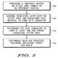
- FIG. 3illustrates in a simplified diagram, a method of fabricating an antifuse element according to the present invention utilizing standard CMOS fabrication techniques well known in the art.
- MOS device 100 of FIGS. 1 and 2is made to function as an antifuse without performing any additional processing steps beyond those normally undertaken in its manufacture, thus no additional cost.
- a trench process and implant techniqueare performed on a substrate, such as a silicon wafer, to define active area 106 and nwell 112 as is shown at 150 .
- Subsequent growth of a gate oxide on active area 106 and gate material depositioni.e.
- gate electrode 104is patterned to form at least one end corner overlaying the active area as is shown at 154 .
- Gate electrode 104is fabricated so that end corners 120 and 122 overlay active area 106 .
- gate electrode 104is defined by a plurality of end corners fabricated to overlay active area 106 , thereby providing for rupture points at the plurality of end corners.
- An nwell contactis fabricated as near as possible to the overlying end corners to minimize a post program conducting path.
- Source and drain implant, interdielectric layer deposition, contact etch, and additional back-end processesare performed as is shown at 156 to complete antifuse element 102 .
- FIGS. 4-7illustrate alternative array layouts formed by integrating a plurality of the antifuse elements of the present invention.
- a plurality of antifuse elements formed according to the previously described embodimentsare utilized. More specifically, FIG. 4 , illustrates an electrically redundant antifuse array (ERAA) 300 formed according to the present invention.
- Array 300comprises a plurality of antifuse elements 302 formed on a substrate 305 similar to antifuse element 102 of FIGS. 1-2 .
- Antifuse elements 302are formed atop separate nwells 306 and include separate active areas 304 for each antifuse element 302 .
- This type of array layoutprovides for electrical isolation between the plurality of antifuse elements 302 that comprise array 300 . Individual programming of each antifuse element is achieved through conductor terminals 310 and diffusion or well terminals 314 .
- the electrical isolation that provides for individual programming of antifuse elements 302increases flexibility and the packing density of array 300 .
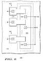
- FIG. 5illustrates an alternative embodiment of an array layout according to the present invention.
- a plurality of antifuse elements 322are formed that share a common active area 324 , and thus a common terminal 334 .
- Antifuse elements 322 and more specifically, a plurality of gate electrodes 326are programmable through a plurality of contacts 328 via a plurality of gate terminals 330 and a plurality of diffusion or well contacts 332 via a plurality of terminals 334 .
- This type of layoutprovides for further increased packing density.
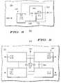
- FIG. 6is a top schematic view of yet another embodiment of an electrically redundant antifuse array 400 formed on a substrate 401 according to the present invention including a plurality of antifuse elements 402 , each defined by a gate electrode 404 and a common active area 405 .
- a plurality of diffusion or well contacts 408are formed on an uppermost surface of common active areas 405 .
- each individual antifuse element 402and more particularly a plurality of end corners 406 of each gate electrode 404 where the highest electric fields are created, is associated with multiple diffusion or well contacts 408 resulting in lower device resistance after programming is complete. This configuration provides for increased packing density.
- FIG. 7illustrates a further embodiment of an electrically redundant antifuse array 420 formed on a substrate 421 .
- Array 420is comprised of a plurality of antifuse elements 422 as previously described in conjunction with FIGS. 1-2 .
- Antifuse elements 422are defined by a plurality of gate electrodes 424 that are positioned in an interleaving configuration about a common active area 426 .
- a plurality of end corners 428 of each individual gate electrode 424are in close electrical contact with a plurality of diffusion or well contacts 430 .
- each individual gate electrodeis in close electrical contact with at least three diffusion or well contacts resulting in low post program resistance and increased packing density.
- FIGS. 8-9are top schematic views of yet another embodiment of the present invention illustrating a semiconductor device 500 , and more particularly an antifuse element 502 formed on a substrate 501 as a unique gate capacitor comprising a gate material and a second conductor comprising an active area bounded by shallow trench isolation.
- antifuse element 502comprises a gate electrode 504 and an active area 506 , which also serves as an electrode.
- Gate electrode 504is formed of n-doped polysilicon and serves as a top electrode for antifuse element 502 .
- Gate electrode 504has a minimum width in a given technology, generally submicron, which extends to overlay at least a portion of active area 506 .
- gate electrode 504is formed of a polysilicon material as is well known in the art and includes a contact 508 positioned on an uppermost surface thereof and terminal 509 , a first end corner 520 and second end corner 522 . Gate electrode 504 is positioned to extend over active area 506 , which serves as the bottom electrode. An insulative material (not shown), is formed therebetween gate electrode 504 and active area 506 . Gate electrode 504 extends over the insulative material and a portion of active area 506 .
- Active area 506includes a highly doped nwell 512 , to have the same doping type as gate electrode 504 . It is anticipated that in the alternative, active area 506 will include a highly doped pwell, when the gate electrode is p-doped.
- a diffusion or well contact 514serves as a contact to nwell 512 and is formed proximate an end 516 of overlying gate electrode 504 . It is a design goal to provide for minimum spacing between end 516 of overlying gate electrode 504 and diffusion or well contact 514 to allow for a lower post program resistance and variation.
- Programming of antifuse element 502involves applying a programming voltage between gate electrode 504 and active area, or bottom electrode, 506 through a gate terminal 509 and a terminal 517 .
- gate electrode 504is formed having only first end corner 520 overlying active area 506 , or falling “within” active area 506 .
- Second end corner 522lies outside active area 506 .
- a vertical current pathis created between gate electrode 504 and active area 506 , the bottom electrode.
- the highest electric fieldwill inherently occur at first end corner 520 of gate electrode 504 that overlays active region 506 due to its being located where the conducting path is shortest to an nwell contact 514 . Controlled rupture of antifuse element 502 at end corner 520 leads to lower resistance between gate electrode 504 and active area 506 .
- antifuse element 502requires only the positioning of a single end corner, first end corner 520 , to overlie active area 506 , and thus fall “within” active area 106 .
- This arrangementprovides an array 550 formed on a substrate 501 , having a layout as illustrated in FIG. 9 in which a plurality of antifuse elements 502 are formed and share a single active area 506 .
- array 550is densely packed in parallel in the common active area 506 , which will result in an electrically redundant antifuse array (ERAA) with simplified supporting circuits.
- ESAelectrically redundant antifuse array
- Typical fuses or antifusesare one time programmable. Once the fuses are programmed, it is impossible to reverse the states (open or short). Thus, typical fuse and antifuse programming is a permanent event.
- the spare antifusescan be utilized to re-program the IC device, thereby forming an electrically redundant antifuse array (ERAA).
- an antifuse elementcomprises: a substrate material having an active area formed in an uppermost surface; a gate electrode having an end corner positioned above the active area; and an insulating layer disposed between the gate electrode and the active area such that a voltage between the gate electrode and the active area creates a current path through the insulating layer and an electric field at the end corner of the gate electrode positioned above the active area, causing a rupture of the insulating layer at a point beneath the end corner of the gate electrode.
- the antifuse elementcan further include the gate electrode having a first end corner and a second end corner positioned above the active area, such that the voltage between the gate electrode and the active area creates an electric field at the first end corner and the second end corner of the gate electrode, causing a rupture of the insulating layer at a point beneath each of the first and second end corners of the gate electrode.
- the substrate materialis typically a semiconductor material.
- the active areacomprises an electrically conductive doped region and the insulating layer comprises a gate oxide.
- a method of an antifuse elementcomprising: providing a substrate material having an active area formed in an uppermost surface; forming a gate electrode having an end corner positioned above the active area; and forming an insulating layer disposed between the gate electrode and the active area such that a voltage between the gate electrode and the active area creates a current path through the insulating layer and an electric field at the end corner positioned above the active area, causing a rupture of the insulating layer at a point beneath the end corner.
- the step of forming a gate electrodecan further include forming a gate electrode having a first end corner and a second end corner positioned above the active area, such that the voltage between the gate electrode and the active area creates an electric field at the first end corner and the second end corner, causing a rupture of the insulating layer at a point beneath each of the first and second end corners.
- an electrically redundant antifuse arraycomprising a plurality of antifuse elements formed on a substrate.
- Each antifuse element of the arraycomprising: an active area formed in an uppermost surface of the substrate; a gate electrode having an end corner positioned above the active area; and an insulating layer disposed between the gate electrode and the active area such that a voltage between the gate electrode and the active area creates a current path through the insulating layer and an electric field at the end corner positioned above the active area, causing a rupture of the insulating layer at a point beneath the end corner of the gate electrode.
- an arrayincluding: an array wherein the active area of each of the plurality of antifuse elements is individually programmable; an array wherein the plurality of antifuse elements are formed having a common active area and are commonly programmable; an array wherein each of the plurality of antifuse elements has a first end corner and a second end corner that overlies the common active area; an array wherein the first end corner and the second end corner of each of the plurality of gate electrodes are in electrical communication with a plurality of well contacts; an array wherein the plurality of antifuse elements are formed on opposing sides of an uppermost surface of the substrate, having end corners of the plurality of gate electrodes interleaved; and an array wherein the first end corner and the second end corner of each of the plurality of gate electrodes are in electrical communication with a single well contact.
Landscapes
- Physics & Mathematics (AREA)
- Condensed Matter Physics & Semiconductors (AREA)
- General Physics & Mathematics (AREA)
- Engineering & Computer Science (AREA)
- Computer Hardware Design (AREA)
- Microelectronics & Electronic Packaging (AREA)
- Power Engineering (AREA)
- Design And Manufacture Of Integrated Circuits (AREA)
- Semiconductor Memories (AREA)
Abstract
Description
Claims (18)
Priority Applications (3)
| Application Number | Priority Date | Filing Date | Title |
|---|---|---|---|
| US11/095,302US7256471B2 (en) | 2005-03-31 | 2005-03-31 | Antifuse element and electrically redundant antifuse array for controlled rupture location |
| PCT/US2006/003530WO2006107384A1 (en) | 2005-03-31 | 2006-02-01 | Antifuse element and electrically redundant antifuse array for controlled rupture location |
| TW95106399ATWI469339B (en) | 2005-03-31 | 2006-02-24 | Antifuse element and electrically redundant antifuse array for controlled rupture location |
Applications Claiming Priority (1)
| Application Number | Priority Date | Filing Date | Title |
|---|---|---|---|
| US11/095,302US7256471B2 (en) | 2005-03-31 | 2005-03-31 | Antifuse element and electrically redundant antifuse array for controlled rupture location |
Publications (2)
| Publication Number | Publication Date |
|---|---|
| US20060226509A1 US20060226509A1 (en) | 2006-10-12 |
| US7256471B2true US7256471B2 (en) | 2007-08-14 |
Family
ID=37073777
Family Applications (1)
| Application Number | Title | Priority Date | Filing Date |
|---|---|---|---|
| US11/095,302Expired - Fee RelatedUS7256471B2 (en) | 2005-03-31 | 2005-03-31 | Antifuse element and electrically redundant antifuse array for controlled rupture location |
Country Status (3)
| Country | Link |
|---|---|
| US (1) | US7256471B2 (en) |
| TW (1) | TWI469339B (en) |
| WO (1) | WO2006107384A1 (en) |
Cited By (7)
| Publication number | Priority date | Publication date | Assignee | Title |
|---|---|---|---|---|
| US20090189248A1 (en)* | 2008-01-30 | 2009-07-30 | Elpida Memory, Inc. | Semiconductor device and method of manufacturing the same |
| US20100164603A1 (en)* | 2008-12-30 | 2010-07-01 | Hafez Walid M | Programmable fuse and anti-fuse elements and methods of changing conduction states of same |
| US20100213570A1 (en)* | 2009-02-25 | 2010-08-26 | Freescale Semiconductor, Inc. | Antifuse |
| US20100230781A1 (en)* | 2009-03-10 | 2010-09-16 | International Business Machines Corporation | Trench anti-fuse structures for a programmable integrated circuit |
| US7825479B2 (en) | 2008-08-06 | 2010-11-02 | International Business Machines Corporation | Electrical antifuse having a multi-thickness dielectric layer |
| US8824114B2 (en) | 2010-04-21 | 2014-09-02 | Freescale Semiconductor, Inc. | Monitor circuit for determining the lifetime of a semiconductor device |
| US9589967B2 (en) | 2014-01-21 | 2017-03-07 | Nxp Usa, Inc. | Fast programming antifuse and method of manufacture |
Families Citing this family (12)
| Publication number | Priority date | Publication date | Assignee | Title |
|---|---|---|---|---|
| US20090132645A1 (en)* | 2007-11-16 | 2009-05-21 | Iac Search & Media, Inc. | User interface and method in a local search system with multiple-field comparison |
| US20090132514A1 (en)* | 2007-11-16 | 2009-05-21 | Iac Search & Media, Inc. | method and system for building text descriptions in a search database |
| US20090132505A1 (en)* | 2007-11-16 | 2009-05-21 | Iac Search & Media, Inc. | Transformation in a system and method for conducting a search |
| US20090132513A1 (en)* | 2007-11-16 | 2009-05-21 | Iac Search & Media, Inc. | Correlation of data in a system and method for conducting a search |
| JP2012099625A (en)* | 2010-11-02 | 2012-05-24 | Renesas Electronics Corp | Semiconductor device |
| US9842802B2 (en) | 2012-06-29 | 2017-12-12 | Qualcomm Incorporated | Integrated circuit device featuring an antifuse and method of making same |
| US9502424B2 (en) | 2012-06-29 | 2016-11-22 | Qualcomm Incorporated | Integrated circuit device featuring an antifuse and method of making same |
| CN103943669B (en)* | 2013-01-22 | 2017-11-14 | 中芯国际集成电路制造(上海)有限公司 | A kind of anti-fuse structures and preparation method thereof |
| WO2015148944A1 (en)* | 2014-03-27 | 2015-10-01 | Qualcomm Incorporated | Integrated circuit device featuring an antifuse and method of making same |
| US9953990B1 (en)* | 2017-08-01 | 2018-04-24 | Synopsys, Inc. | One-time programmable memory using rupturing of gate insulation |
| US10964708B2 (en)* | 2018-06-26 | 2021-03-30 | Micron Technology, Inc. | Fuse-array element |
| US11393547B2 (en)* | 2019-11-26 | 2022-07-19 | Piecemakers Technology, Inc. | Anti-fuse one-time programmable memory cell and related array structure |
Citations (9)
| Publication number | Priority date | Publication date | Assignee | Title |
|---|---|---|---|---|
| US6130469A (en)* | 1998-04-24 | 2000-10-10 | International Business Machines Corporation | Electrically alterable antifuse using FET |
| US6396120B1 (en) | 2000-03-17 | 2002-05-28 | International Business Machines Corporation | Silicon anti-fuse structures, bulk and silicon on insulator fabrication methods and application |
| US6515344B1 (en)* | 1999-10-28 | 2003-02-04 | Advanced Micro Devices, Inc. | Thin oxide anti-fuse |
| US6597234B2 (en) | 2001-12-14 | 2003-07-22 | Motorola, Inc. | Anti-fuse circuit and method of operation |
| US6753590B2 (en) | 2002-07-08 | 2004-06-22 | International Business Machines Corporation | High impedance antifuse |
| US6774439B2 (en) | 2000-02-17 | 2004-08-10 | Kabushiki Kaisha Toshiba | Semiconductor device using fuse/anti-fuse system |
| US6775197B2 (en) | 2002-11-27 | 2004-08-10 | Novocell Semiconductor, Inc. | Non-volatile memory element integratable with standard CMOS circuitry and related programming methods and embedded memories |
| US20040223363A1 (en)* | 2002-04-26 | 2004-11-11 | Peng Jack Zezhong | High density semiconductor memory cell and memory array using a single transistor and having counter-doped poly and buried diffusion wordline |
| US20060092742A1 (en)* | 2004-11-01 | 2006-05-04 | Fabrice Paillet | OTP antifuse cell and cell array |
Family Cites Families (2)
| Publication number | Priority date | Publication date | Assignee | Title |
|---|---|---|---|---|
| TW517344B (en)* | 2001-05-28 | 2003-01-11 | United Microelectronics Corp | Manufacturing method of anti-fuse structure |
| US6580144B2 (en)* | 2001-09-28 | 2003-06-17 | Hewlett-Packard Development Company, L.P. | One time programmable fuse/anti-fuse combination based memory cell |
- 2005
- 2005-03-31USUS11/095,302patent/US7256471B2/ennot_activeExpired - Fee Related
- 2006
- 2006-02-01WOPCT/US2006/003530patent/WO2006107384A1/enactiveApplication Filing
- 2006-02-24TWTW95106399Apatent/TWI469339B/ennot_activeIP Right Cessation
Patent Citations (9)
| Publication number | Priority date | Publication date | Assignee | Title |
|---|---|---|---|---|
| US6130469A (en)* | 1998-04-24 | 2000-10-10 | International Business Machines Corporation | Electrically alterable antifuse using FET |
| US6515344B1 (en)* | 1999-10-28 | 2003-02-04 | Advanced Micro Devices, Inc. | Thin oxide anti-fuse |
| US6774439B2 (en) | 2000-02-17 | 2004-08-10 | Kabushiki Kaisha Toshiba | Semiconductor device using fuse/anti-fuse system |
| US6396120B1 (en) | 2000-03-17 | 2002-05-28 | International Business Machines Corporation | Silicon anti-fuse structures, bulk and silicon on insulator fabrication methods and application |
| US6597234B2 (en) | 2001-12-14 | 2003-07-22 | Motorola, Inc. | Anti-fuse circuit and method of operation |
| US20040223363A1 (en)* | 2002-04-26 | 2004-11-11 | Peng Jack Zezhong | High density semiconductor memory cell and memory array using a single transistor and having counter-doped poly and buried diffusion wordline |
| US6753590B2 (en) | 2002-07-08 | 2004-06-22 | International Business Machines Corporation | High impedance antifuse |
| US6775197B2 (en) | 2002-11-27 | 2004-08-10 | Novocell Semiconductor, Inc. | Non-volatile memory element integratable with standard CMOS circuitry and related programming methods and embedded memories |
| US20060092742A1 (en)* | 2004-11-01 | 2006-05-04 | Fabrice Paillet | OTP antifuse cell and cell array |
Cited By (12)
| Publication number | Priority date | Publication date | Assignee | Title |
|---|---|---|---|---|
| US20090189248A1 (en)* | 2008-01-30 | 2009-07-30 | Elpida Memory, Inc. | Semiconductor device and method of manufacturing the same |
| US8729642B2 (en) | 2008-01-30 | 2014-05-20 | Eiji Kitamura | Semiconductor device comprising a gate electrode having an opening |
| US7825479B2 (en) | 2008-08-06 | 2010-11-02 | International Business Machines Corporation | Electrical antifuse having a multi-thickness dielectric layer |
| US20100164603A1 (en)* | 2008-12-30 | 2010-07-01 | Hafez Walid M | Programmable fuse and anti-fuse elements and methods of changing conduction states of same |
| US8101471B2 (en)* | 2008-12-30 | 2012-01-24 | Intel Corporation | Method of forming programmable anti-fuse element |
| US20100213570A1 (en)* | 2009-02-25 | 2010-08-26 | Freescale Semiconductor, Inc. | Antifuse |
| US8049299B2 (en) | 2009-02-25 | 2011-11-01 | Freescale Semiconductor, Inc. | Antifuses with curved breakdown regions |
| US8329514B2 (en) | 2009-02-25 | 2012-12-11 | Freescale Semiconductor, Inc. | Methods for forming antifuses with curved breakdown regions |
| US20100230781A1 (en)* | 2009-03-10 | 2010-09-16 | International Business Machines Corporation | Trench anti-fuse structures for a programmable integrated circuit |
| US7977766B2 (en)* | 2009-03-10 | 2011-07-12 | International Business Machines Corporation | Trench anti-fuse structures for a programmable integrated circuit |
| US8824114B2 (en) | 2010-04-21 | 2014-09-02 | Freescale Semiconductor, Inc. | Monitor circuit for determining the lifetime of a semiconductor device |
| US9589967B2 (en) | 2014-01-21 | 2017-03-07 | Nxp Usa, Inc. | Fast programming antifuse and method of manufacture |
Also Published As
| Publication number | Publication date |
|---|---|
| TW200711121A (en) | 2007-03-16 |
| TWI469339B (en) | 2015-01-11 |
| US20060226509A1 (en) | 2006-10-12 |
| WO2006107384A1 (en) | 2006-10-12 |
Similar Documents
| Publication | Publication Date | Title |
|---|---|---|
| WO2006107384A1 (en) | Antifuse element and electrically redundant antifuse array for controlled rupture location | |
| US7834417B2 (en) | Antifuse elements | |
| TWI399847B (en) | Tunable antifuse element and method of manufacture | |
| KR101006123B1 (en) | Electrically programmable fuses for insulator-phase-silicon (SOI) technology | |
| US6803804B2 (en) | Programmable latch array using antifuses | |
| US8299570B2 (en) | Efuse containing sige stack | |
| US6525399B2 (en) | Junctionless antifuses and systems containing junctionless antifuses | |
| US7269898B2 (en) | Method for making an edge intensive antifuse | |
| JPH0722513A (en) | Semiconductor device and manufacturing method thereof | |
| US8766374B2 (en) | One-time programmable semiconductor device | |
| US20090029541A1 (en) | Method of fabricating anti-fuse and method of programming anti-fuse | |
| JP2003115537A (en) | Anti-fuse element, semiconductor device, and method of programming semiconductor device |
Legal Events
| Date | Code | Title | Description |
|---|---|---|---|
| AS | Assignment | Owner name:FREESCALE SEMICONDUCTOR, INC., TEXAS Free format text:ASSIGNMENT OF ASSIGNORS INTEREST;ASSIGNORS:MIN, WON GI;BAIRD, ROBERT W.;LEE, GORDON P.;AND OTHERS;REEL/FRAME:016442/0887;SIGNING DATES FROM 20050329 TO 20050330 | |
| FEPP | Fee payment procedure | Free format text:PAYOR NUMBER ASSIGNED (ORIGINAL EVENT CODE: ASPN); ENTITY STATUS OF PATENT OWNER: LARGE ENTITY | |
| AS | Assignment | Owner name:CITIBANK, N.A. AS COLLATERAL AGENT, NEW YORK Free format text:SECURITY AGREEMENT;ASSIGNORS:FREESCALE SEMICONDUCTOR, INC.;FREESCALE ACQUISITION CORPORATION;FREESCALE ACQUISITION HOLDINGS CORP.;AND OTHERS;REEL/FRAME:018855/0129 Effective date:20061201 Owner name:CITIBANK, N.A. AS COLLATERAL AGENT,NEW YORK Free format text:SECURITY AGREEMENT;ASSIGNORS:FREESCALE SEMICONDUCTOR, INC.;FREESCALE ACQUISITION CORPORATION;FREESCALE ACQUISITION HOLDINGS CORP.;AND OTHERS;REEL/FRAME:018855/0129 Effective date:20061201 | |
| STCF | Information on status: patent grant | Free format text:PATENTED CASE | |
| AS | Assignment | Owner name:CITIBANK, N.A., NEW YORK Free format text:SECURITY AGREEMENT;ASSIGNOR:FREESCALE SEMICONDUCTOR, INC.;REEL/FRAME:020518/0215 Effective date:20071025 Owner name:CITIBANK, N.A.,NEW YORK Free format text:SECURITY AGREEMENT;ASSIGNOR:FREESCALE SEMICONDUCTOR, INC.;REEL/FRAME:020518/0215 Effective date:20071025 | |
| AS | Assignment | Owner name:CITIBANK, N.A., AS COLLATERAL AGENT,NEW YORK Free format text:SECURITY AGREEMENT;ASSIGNOR:FREESCALE SEMICONDUCTOR, INC.;REEL/FRAME:024397/0001 Effective date:20100413 Owner name:CITIBANK, N.A., AS COLLATERAL AGENT, NEW YORK Free format text:SECURITY AGREEMENT;ASSIGNOR:FREESCALE SEMICONDUCTOR, INC.;REEL/FRAME:024397/0001 Effective date:20100413 | |
| FPAY | Fee payment | Year of fee payment:4 | |
| AS | Assignment | Owner name:CITIBANK, N.A., AS NOTES COLLATERAL AGENT, NEW YORK Free format text:SECURITY AGREEMENT;ASSIGNOR:FREESCALE SEMICONDUCTOR, INC.;REEL/FRAME:030633/0424 Effective date:20130521 Owner name:CITIBANK, N.A., AS NOTES COLLATERAL AGENT, NEW YOR Free format text:SECURITY AGREEMENT;ASSIGNOR:FREESCALE SEMICONDUCTOR, INC.;REEL/FRAME:030633/0424 Effective date:20130521 | |
| AS | Assignment | Owner name:CITIBANK, N.A., AS NOTES COLLATERAL AGENT, NEW YORK Free format text:SECURITY AGREEMENT;ASSIGNOR:FREESCALE SEMICONDUCTOR, INC.;REEL/FRAME:031591/0266 Effective date:20131101 Owner name:CITIBANK, N.A., AS NOTES COLLATERAL AGENT, NEW YOR Free format text:SECURITY AGREEMENT;ASSIGNOR:FREESCALE SEMICONDUCTOR, INC.;REEL/FRAME:031591/0266 Effective date:20131101 | |
| FPAY | Fee payment | Year of fee payment:8 | |
| AS | Assignment | Owner name:FREESCALE SEMICONDUCTOR, INC., TEXAS Free format text:PATENT RELEASE;ASSIGNOR:CITIBANK, N.A., AS COLLATERAL AGENT;REEL/FRAME:037354/0225 Effective date:20151207 Owner name:FREESCALE SEMICONDUCTOR, INC., TEXAS Free format text:PATENT RELEASE;ASSIGNOR:CITIBANK, N.A., AS COLLATERAL AGENT;REEL/FRAME:037356/0143 Effective date:20151207 Owner name:FREESCALE SEMICONDUCTOR, INC., TEXAS Free format text:PATENT RELEASE;ASSIGNOR:CITIBANK, N.A., AS COLLATERAL AGENT;REEL/FRAME:037354/0704 Effective date:20151207 Owner name:FREESCALE SEMICONDUCTOR, INC., TEXAS Free format text:PATENT RELEASE;ASSIGNOR:CITIBANK, N.A., AS COLLATERAL AGENT;REEL/FRAME:037356/0553 Effective date:20151207 | |
| AS | Assignment | Owner name:MORGAN STANLEY SENIOR FUNDING, INC., MARYLAND Free format text:ASSIGNMENT AND ASSUMPTION OF SECURITY INTEREST IN PATENTS;ASSIGNOR:CITIBANK, N.A.;REEL/FRAME:037486/0517 Effective date:20151207 | |
| AS | Assignment | Owner name:MORGAN STANLEY SENIOR FUNDING, INC., MARYLAND Free format text:ASSIGNMENT AND ASSUMPTION OF SECURITY INTEREST IN PATENTS;ASSIGNOR:CITIBANK, N.A.;REEL/FRAME:037518/0292 Effective date:20151207 | |
| AS | Assignment | Owner name:NORTH STAR INNOVATIONS INC., CALIFORNIA Free format text:ASSIGNMENT OF ASSIGNORS INTEREST;ASSIGNOR:FREESCALE SEMICONDUCTOR, INC.;REEL/FRAME:037694/0264 Effective date:20151002 | |
| AS | Assignment | Owner name:NXP, B.V., F/K/A FREESCALE SEMICONDUCTOR, INC., NETHERLANDS Free format text:RELEASE BY SECURED PARTY;ASSIGNOR:MORGAN STANLEY SENIOR FUNDING, INC.;REEL/FRAME:040925/0001 Effective date:20160912 Owner name:NXP, B.V., F/K/A FREESCALE SEMICONDUCTOR, INC., NE Free format text:RELEASE BY SECURED PARTY;ASSIGNOR:MORGAN STANLEY SENIOR FUNDING, INC.;REEL/FRAME:040925/0001 Effective date:20160912 | |
| AS | Assignment | Owner name:NXP B.V., NETHERLANDS Free format text:RELEASE BY SECURED PARTY;ASSIGNOR:MORGAN STANLEY SENIOR FUNDING, INC.;REEL/FRAME:040928/0001 Effective date:20160622 | |
| AS | Assignment | Owner name:MORGAN STANLEY SENIOR FUNDING, INC., MARYLAND Free format text:CORRECTIVE ASSIGNMENT TO CORRECT THE REMOVE PATENTS 8108266 AND 8062324 AND REPLACE THEM WITH 6108266 AND 8060324 PREVIOUSLY RECORDED ON REEL 037518 FRAME 0292. ASSIGNOR(S) HEREBY CONFIRMS THE ASSIGNMENT AND ASSUMPTION OF SECURITY INTEREST IN PATENTS;ASSIGNOR:CITIBANK, N.A.;REEL/FRAME:041703/0536 Effective date:20151207 | |
| AS | Assignment | Owner name:SHENZHEN XINGUODU TECHNOLOGY CO., LTD., CHINA Free format text:CORRECTIVE ASSIGNMENT TO CORRECT THE TO CORRECT THE APPLICATION NO. FROM 13,883,290 TO 13,833,290 PREVIOUSLY RECORDED ON REEL 041703 FRAME 0536. ASSIGNOR(S) HEREBY CONFIRMS THE THE ASSIGNMENT AND ASSUMPTION OF SECURITYINTEREST IN PATENTS.;ASSIGNOR:MORGAN STANLEY SENIOR FUNDING, INC.;REEL/FRAME:048734/0001 Effective date:20190217 | |
| FEPP | Fee payment procedure | Free format text:MAINTENANCE FEE REMINDER MAILED (ORIGINAL EVENT CODE: REM.); ENTITY STATUS OF PATENT OWNER: LARGE ENTITY | |
| LAPS | Lapse for failure to pay maintenance fees | Free format text:PATENT EXPIRED FOR FAILURE TO PAY MAINTENANCE FEES (ORIGINAL EVENT CODE: EXP.); ENTITY STATUS OF PATENT OWNER: LARGE ENTITY | |
| STCH | Information on status: patent discontinuation | Free format text:PATENT EXPIRED DUE TO NONPAYMENT OF MAINTENANCE FEES UNDER 37 CFR 1.362 | |
| FP | Lapsed due to failure to pay maintenance fee | Effective date:20190814 | |
| AS | Assignment | Owner name:MORGAN STANLEY SENIOR FUNDING, INC., MARYLAND Free format text:CORRECTIVE ASSIGNMENT TO CORRECT THE REMOVE APPLICATION11759915 AND REPLACE IT WITH APPLICATION 11759935 PREVIOUSLY RECORDED ON REEL 037486 FRAME 0517. ASSIGNOR(S) HEREBY CONFIRMS THE ASSIGNMENT AND ASSUMPTION OF SECURITYINTEREST IN PATENTS;ASSIGNOR:CITIBANK, N.A.;REEL/FRAME:053547/0421 Effective date:20151207 | |
| AS | Assignment | Owner name:NXP B.V., NETHERLANDS Free format text:CORRECTIVE ASSIGNMENT TO CORRECT THE REMOVEAPPLICATION 11759915 AND REPLACE IT WITH APPLICATION11759935 PREVIOUSLY RECORDED ON REEL 040928 FRAME 0001. ASSIGNOR(S) HEREBY CONFIRMS THE RELEASE OF SECURITYINTEREST;ASSIGNOR:MORGAN STANLEY SENIOR FUNDING, INC.;REEL/FRAME:052915/0001 Effective date:20160622 | |
| AS | Assignment | Owner name:NXP, B.V. F/K/A FREESCALE SEMICONDUCTOR, INC., NETHERLANDS Free format text:CORRECTIVE ASSIGNMENT TO CORRECT THE REMOVEAPPLICATION 11759915 AND REPLACE IT WITH APPLICATION11759935 PREVIOUSLY RECORDED ON REEL 040925 FRAME 0001. ASSIGNOR(S) HEREBY CONFIRMS THE RELEASE OF SECURITYINTEREST;ASSIGNOR:MORGAN STANLEY SENIOR FUNDING, INC.;REEL/FRAME:052917/0001 Effective date:20160912 |