US7255800B1 - Wet etching process - Google Patents
Wet etching processDownload PDFInfo
- Publication number
- US7255800B1 US7255800B1US10/710,984US71098404AUS7255800B1US 7255800 B1US7255800 B1US 7255800B1US 71098404 AUS71098404 AUS 71098404AUS 7255800 B1US7255800 B1US 7255800B1
- Authority
- US
- United States
- Prior art keywords
- wafer
- etching
- silicon
- junction
- dopant
- Prior art date
- Legal status (The legal status is an assumption and is not a legal conclusion. Google has not performed a legal analysis and makes no representation as to the accuracy of the status listed.)
- Expired - Fee Related
Links
- 238000000034methodMethods0.000titleclaimsabstractdescription40
- 238000001039wet etchingMethods0.000titleclaimsabstractdescription16
- 238000005530etchingMethods0.000claimsabstractdescription33
- XUIMIQQOPSSXEZ-UHFFFAOYSA-NSiliconChemical compound[Si]XUIMIQQOPSSXEZ-UHFFFAOYSA-N0.000claimsabstractdescription25
- 229910052710siliconInorganic materials0.000claimsabstractdescription25
- 239000010703siliconSubstances0.000claimsabstractdescription25
- 229910021426porous siliconInorganic materials0.000claimsabstractdescription14
- 238000004090dissolutionMethods0.000claimsabstractdescription5
- KWYUFKZDYYNOTN-UHFFFAOYSA-MPotassium hydroxideChemical compound[OH-].[K+]KWYUFKZDYYNOTN-UHFFFAOYSA-M0.000claimsdescription32
- WGTYBPLFGIVFAS-UHFFFAOYSA-Mtetramethylammonium hydroxideChemical compound[OH-].C[N+](C)(C)CWGTYBPLFGIVFAS-UHFFFAOYSA-M0.000claimsdescription12
- 239000002019doping agentSubstances0.000claimsdescription11
- KRHYYFGTRYWZRS-UHFFFAOYSA-NFluoraneChemical compoundFKRHYYFGTRYWZRS-UHFFFAOYSA-N0.000claimsdescription6
- 238000009792diffusion processMethods0.000claimsdescription5
- 238000000059patterningMethods0.000claimsdescription5
- 238000004544sputter depositionMethods0.000claimsdescription2
- 230000015572biosynthetic processEffects0.000abstractdescription3
- 238000004519manufacturing processMethods0.000description5
- 238000001312dry etchingMethods0.000description4
- 239000011148porous materialSubstances0.000description2
- 238000010276constructionMethods0.000description1
- 238000000708deep reactive-ion etchingMethods0.000description1
- 230000000977initiatory effectEffects0.000description1
- 238000004377microelectronicMethods0.000description1
- XUIMIQQOPSSXEZ-NJFSPNSNSA-Nsilicon-30 atomChemical compound[30Si]XUIMIQQOPSSXEZ-NJFSPNSNSA-N0.000description1
- 239000000126substanceSubstances0.000description1
Images


Classifications
- B—PERFORMING OPERATIONS; TRANSPORTING
- B81—MICROSTRUCTURAL TECHNOLOGY
- B81C—PROCESSES OR APPARATUS SPECIALLY ADAPTED FOR THE MANUFACTURE OR TREATMENT OF MICROSTRUCTURAL DEVICES OR SYSTEMS
- B81C1/00—Manufacture or treatment of devices or systems in or on a substrate
- B81C1/00436—Shaping materials, i.e. techniques for structuring the substrate or the layers on the substrate
- B81C1/005—Bulk micromachining
- B—PERFORMING OPERATIONS; TRANSPORTING
- B81—MICROSTRUCTURAL TECHNOLOGY
- B81C—PROCESSES OR APPARATUS SPECIALLY ADAPTED FOR THE MANUFACTURE OR TREATMENT OF MICROSTRUCTURAL DEVICES OR SYSTEMS
- B81C1/00—Manufacture or treatment of devices or systems in or on a substrate
- B81C1/00436—Shaping materials, i.e. techniques for structuring the substrate or the layers on the substrate
- B81C1/00555—Achieving a desired geometry, i.e. controlling etch rates, anisotropy or selectivity
- B81C1/00619—Forming high aspect ratio structures having deep steep walls
- H—ELECTRICITY
- H01—ELECTRIC ELEMENTS
- H01L—SEMICONDUCTOR DEVICES NOT COVERED BY CLASS H10
- H01L21/00—Processes or apparatus adapted for the manufacture or treatment of semiconductor or solid state devices or of parts thereof
- H01L21/02—Manufacture or treatment of semiconductor devices or of parts thereof
- H01L21/02041—Cleaning
- H01L21/02043—Cleaning before device manufacture, i.e. Begin-Of-Line process
- H01L21/02052—Wet cleaning only
- H—ELECTRICITY
- H01—ELECTRIC ELEMENTS
- H01L—SEMICONDUCTOR DEVICES NOT COVERED BY CLASS H10
- H01L21/00—Processes or apparatus adapted for the manufacture or treatment of semiconductor or solid state devices or of parts thereof
- H01L21/02—Manufacture or treatment of semiconductor devices or of parts thereof
- H01L21/04—Manufacture or treatment of semiconductor devices or of parts thereof the devices having potential barriers, e.g. a PN junction, depletion layer or carrier concentration layer
- H01L21/18—Manufacture or treatment of semiconductor devices or of parts thereof the devices having potential barriers, e.g. a PN junction, depletion layer or carrier concentration layer the devices having semiconductor bodies comprising elements of Group IV of the Periodic Table or AIIIBV compounds with or without impurities, e.g. doping materials
- H01L21/30—Treatment of semiconductor bodies using processes or apparatus not provided for in groups H01L21/20 - H01L21/26
- H01L21/302—Treatment of semiconductor bodies using processes or apparatus not provided for in groups H01L21/20 - H01L21/26 to change their surface-physical characteristics or shape, e.g. etching, polishing, cutting
- H01L21/306—Chemical or electrical treatment, e.g. electrolytic etching
- H01L21/3063—Electrolytic etching
- B—PERFORMING OPERATIONS; TRANSPORTING
- B81—MICROSTRUCTURAL TECHNOLOGY
- B81B—MICROSTRUCTURAL DEVICES OR SYSTEMS, e.g. MICROMECHANICAL DEVICES
- B81B2203/00—Basic microelectromechanical structures
- B81B2203/03—Static structures
- B81B2203/0353—Holes
- B—PERFORMING OPERATIONS; TRANSPORTING
- B81—MICROSTRUCTURAL TECHNOLOGY
- B81C—PROCESSES OR APPARATUS SPECIALLY ADAPTED FOR THE MANUFACTURE OR TREATMENT OF MICROSTRUCTURAL DEVICES OR SYSTEMS
- B81C2201/00—Manufacture or treatment of microstructural devices or systems
- B81C2201/01—Manufacture or treatment of microstructural devices or systems in or on a substrate
- B81C2201/0101—Shaping material; Structuring the bulk substrate or layers on the substrate; Film patterning
- B81C2201/0111—Bulk micromachining
- B81C2201/0115—Porous silicon
- B—PERFORMING OPERATIONS; TRANSPORTING
- B81—MICROSTRUCTURAL TECHNOLOGY
- B81C—PROCESSES OR APPARATUS SPECIALLY ADAPTED FOR THE MANUFACTURE OR TREATMENT OF MICROSTRUCTURAL DEVICES OR SYSTEMS
- B81C2201/00—Manufacture or treatment of microstructural devices or systems
- B81C2201/01—Manufacture or treatment of microstructural devices or systems in or on a substrate
- B81C2201/0101—Shaping material; Structuring the bulk substrate or layers on the substrate; Film patterning
- B81C2201/0128—Processes for removing material
- B81C2201/013—Etching
- B81C2201/0133—Wet etching
- B—PERFORMING OPERATIONS; TRANSPORTING
- B81—MICROSTRUCTURAL TECHNOLOGY
- B81C—PROCESSES OR APPARATUS SPECIALLY ADAPTED FOR THE MANUFACTURE OR TREATMENT OF MICROSTRUCTURAL DEVICES OR SYSTEMS
- B81C2201/00—Manufacture or treatment of microstructural devices or systems
- B81C2201/01—Manufacture or treatment of microstructural devices or systems in or on a substrate
- B81C2201/0101—Shaping material; Structuring the bulk substrate or layers on the substrate; Film patterning
- B81C2201/0128—Processes for removing material
- B81C2201/013—Etching
- B81C2201/0135—Controlling etch progression
- B81C2201/0136—Controlling etch progression by doping limited material regions
Definitions
- MEMS devicesare based on using microelectronic wafer fabrication techniques to produce complex shapes in the ⁇ m to mm size range with embedded sensors, actuators and circuitry. More than a dimension, MEMS is a way of manufacturing.
- bulk silicon etchingare predominantly used namely, wet and dry etching.
- Wet etchingwhile offering process simplicity and low cost requires long hous for etching and results in sharp corners and 54.7-degree side wall angles.
- Dry etching techniquenamely the Deep reactive lon etching (DRIE) overcomes the difficulties of wet etching allowing for arbitrary shapes but in an expensive process.
- DRIEDeep reactive lon etching
- the present inventionprovides a novel wet etching process useful in the fabrication of MEMS devices.
- a bulk silicon etching methodincluding the steps of, providing a silicon wafer, diffusing the wafer with dopant, whereby the diffusion creates a PN-junction throughout the surface of the wafer, providing a mask, positioning the mask in overlying relation to the surface of the wafer,
- the silicon waferis an N-type silicon wafer and the dopant is a P-type dopant.
- the wafermay be a P-type silicon wafer and the dopant may be an N-type dopant.
- Various techniquesare within the scope of the present invention for patterning the oxide layer on the surface of the wafer, including, but not limited to, sputtering.
- etching the oxide patterned on the waferincluding, but not limited to, etching with potassium hydroxide (KOH).
- KOHpotassium hydroxide
- the step of etching the oxideis accomplished by subjecting the wafer to potassium hydroxide etching for approximately ten minutes.
- etching the porous siliconincluding, but not limited to, etching with potassium hydroxide (KOH) and etching with tetramethyl ammonium hydroxide (TMAH).
- KOHpotassium hydroxide
- TMAHtetramethyl ammonium hydroxide
- the porous siliconis subjected to etching utilizing either KOH or TMAH for approximately thirty seconds.
- the method of the present inventionprovides significant lowering of fabrication costs through the utilization of cost effective wet etching techniques.
- the present inventiondiscloses an etching technique which offers the simplicity of wet etching and the process capabilities of dry etching. As such, the method of the present invention results in the rapid fabrication of high aspect ratio anisotropic structures substantially devoid of sidewall angles. Accordingly, the method presented is an alternative to deep reactive ion etching.
- FIG. 1is a cross-sectional illustration of a silicon wafer having a blanket PN-junction throughout the surface of the wafer in accordance with the present invention.
- FIG. 2is a cross-sectional illustration of a silicon wafer patterned with oxide in accordance with the present invention.
- FIG. 3is a cross-sectional illustration of a silicon wafer after the oxide patterned wafer has been subjected to KOH etching in accordance with the present invention.
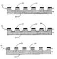
- FIG. 4is a cross-sectional illustration of a silicon wafer after the wafer surface has been subjected to hydrofluoric acid electrochemical etching to form porous silicon in accordance with the present invention.
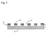
- FIG. 5is a cross-sectional illustration of a silicon wafer, having selective porous silicon, after the wafer has been subjected to KOH etching, resulting in through wafer high aspect ration structures with straight sidewalls.
- the present inventionillustrates a bulk silicon etching technique that yields straight sidewalls, through wafer structures, in very short times using standard silicon wet etching techniques.
- a method employing selective porous silicon formation and dissolutionis used to create high aspect ratio structures with straight sidewalls for through wafer MEMS processing.
- an N-type silicon wafer 10is diffused with P-type dopant to the order of 1020 atoms/cm2. Other ratios are additionally within the scope of the present invention.
- the diffusioncreates a blanket PN-junction 15 through out the surface of the wafer.
- a thin layer of oxide 20is then sputtered and patterned using the desired mass on top of the diffusion, as shown with reference to FIG. 2 .
- the waferis then subjected to KOH etching for ten minutes to create recessed areas 25 where the oxide was patterned, as shown with reference to FIG. 3 .
- the patterning of oxide and the silicon beneathcreates patterns of the surface, which are contrasted by the presence and absence of PN-junction.
- porous silicon 30is formed on the patterned wafer using HF based electrochemical etching technique.
- the poresare formed in areas that are characterized by the absence of surface junction. In the areas which have a surface junction, the junction blocks the pore initiation and propagation due to lack of holes in the depletion region, which are essential to porous silicon formation.
- the resultant waferis selectively porous in the areas where the oxide was patterned and the rest of the wafer is bulk silicon.
- This waferis further subjected to KOH or TMAH etching for thirty seconds which results in rapid dissolution of porous areas, leaving behind bulk silicon, thus resulting in through wafer high aspect ration structures with straight sidewalls 35 .
- the drastic reduction in etching timeis due to the fact that in the porous areas the etching chemical encounters much higher surface area than in the non-porous areas, thus leading to very high selectivity.
Landscapes
- Engineering & Computer Science (AREA)
- Manufacturing & Machinery (AREA)
- Microelectronics & Electronic Packaging (AREA)
- Physics & Mathematics (AREA)
- Condensed Matter Physics & Semiconductors (AREA)
- General Physics & Mathematics (AREA)
- Computer Hardware Design (AREA)
- Power Engineering (AREA)
- Geometry (AREA)
- Weting (AREA)
- Micromachines (AREA)
Abstract
Description
Claims (12)
Priority Applications (2)
| Application Number | Priority Date | Filing Date | Title |
|---|---|---|---|
| US10/710,984US7255800B1 (en) | 2003-08-15 | 2004-08-16 | Wet etching process |
| US11/828,639US7892440B1 (en) | 2003-08-15 | 2007-07-26 | Wet etching process |
Applications Claiming Priority (2)
| Application Number | Priority Date | Filing Date | Title |
|---|---|---|---|
| US48123303P | 2003-08-15 | 2003-08-15 | |
| US10/710,984US7255800B1 (en) | 2003-08-15 | 2004-08-16 | Wet etching process |
Related Child Applications (1)
| Application Number | Title | Priority Date | Filing Date |
|---|---|---|---|
| US11/828,639Continuation-In-PartUS7892440B1 (en) | 2003-08-15 | 2007-07-26 | Wet etching process |
Publications (1)
| Publication Number | Publication Date |
|---|---|
| US7255800B1true US7255800B1 (en) | 2007-08-14 |
Family
ID=38336993
Family Applications (2)
| Application Number | Title | Priority Date | Filing Date |
|---|---|---|---|
| US10/710,984Expired - Fee RelatedUS7255800B1 (en) | 2003-08-15 | 2004-08-16 | Wet etching process |
| US11/828,639Expired - Fee RelatedUS7892440B1 (en) | 2003-08-15 | 2007-07-26 | Wet etching process |
Family Applications After (1)
| Application Number | Title | Priority Date | Filing Date |
|---|---|---|---|
| US11/828,639Expired - Fee RelatedUS7892440B1 (en) | 2003-08-15 | 2007-07-26 | Wet etching process |
Country Status (1)
| Country | Link |
|---|---|
| US (2) | US7255800B1 (en) |
Families Citing this family (2)
| Publication number | Priority date | Publication date | Assignee | Title |
|---|---|---|---|---|
| KR101926539B1 (en)* | 2011-12-13 | 2018-12-10 | 엘지이노텍 주식회사 | Nanowire grid structure and method of manufacturing a nanowire |
| TWI494989B (en)* | 2012-03-08 | 2015-08-01 | Nat Univ Chung Hsing | An electrochemical etching method for forming a high aspect ratio (HAR) characteristic structure in a semiconductor element |
Citations (4)
| Publication number | Priority date | Publication date | Assignee | Title |
|---|---|---|---|---|
| US5830777A (en)* | 1994-10-31 | 1998-11-03 | Kabushiki Kaisha Tokai Rika Denki Seisakusho | Method of manufacturing a capacitance type acceleration sensor |
| US6020250A (en)* | 1994-08-11 | 2000-02-01 | International Business Machines Corporation | Stacked devices |
| US6139758A (en)* | 1996-08-23 | 2000-10-31 | Enlite Laboratories, Inc. | Method of manufacturing a micromachined thermal flowmeter |
| US6358861B1 (en)* | 1999-01-13 | 2002-03-19 | Mitsubishi Denki Kabushiki Kaisha | Manufacturing method of silicon device |
Family Cites Families (5)
| Publication number | Priority date | Publication date | Assignee | Title |
|---|---|---|---|---|
| EP0534474B1 (en)* | 1991-09-27 | 2002-01-16 | Canon Kabushiki Kaisha | Method of processing a silicon substrate |
| JP2001006126A (en)* | 1999-06-17 | 2001-01-12 | Nec Corp | Magneto-resistance effect head, magneto-resistance detection system incorporating the same, and magnetic storage system incorporating the same |
| US6503838B1 (en)* | 1999-12-31 | 2003-01-07 | Texas Instruments Incorporated | Integrated circuit isolation of functionally distinct RF circuits |
| US6736982B2 (en)* | 2001-06-15 | 2004-05-18 | Xiang Zheng Tu | Micromachined vertical vibrating gyroscope |
| US7112525B1 (en)* | 2003-12-22 | 2006-09-26 | University Of South Florida | Method for the assembly of nanowire interconnects |
- 2004
- 2004-08-16USUS10/710,984patent/US7255800B1/ennot_activeExpired - Fee Related
- 2007
- 2007-07-26USUS11/828,639patent/US7892440B1/ennot_activeExpired - Fee Related
Patent Citations (4)
| Publication number | Priority date | Publication date | Assignee | Title |
|---|---|---|---|---|
| US6020250A (en)* | 1994-08-11 | 2000-02-01 | International Business Machines Corporation | Stacked devices |
| US5830777A (en)* | 1994-10-31 | 1998-11-03 | Kabushiki Kaisha Tokai Rika Denki Seisakusho | Method of manufacturing a capacitance type acceleration sensor |
| US6139758A (en)* | 1996-08-23 | 2000-10-31 | Enlite Laboratories, Inc. | Method of manufacturing a micromachined thermal flowmeter |
| US6358861B1 (en)* | 1999-01-13 | 2002-03-19 | Mitsubishi Denki Kabushiki Kaisha | Manufacturing method of silicon device |
Also Published As
| Publication number | Publication date |
|---|---|
| US7892440B1 (en) | 2011-02-22 |
Similar Documents
| Publication | Publication Date | Title |
|---|---|---|
| Kovacs et al. | Bulk micromachining of silicon | |
| WO2007002426A3 (en) | Semiconductor device structures and methods of forming semiconductor structures | |
| US20090232334A1 (en) | Micromechanical Component and Method for its Production | |
| TW200710991A (en) | Semiconductor structures formed on substrates and methods of manufacturing the same | |
| ATE283234T1 (en) | METHOD FOR PRODUCING A MICROFLUID COMPONENT | |
| ATE447538T1 (en) | SOI/GLASS PROCESS FOR PRODUCING THIN MICRO-MACHINED STRUCTURES | |
| US11167982B2 (en) | Semiconductor arrangement and formation thereof | |
| Tjerkstra et al. | Multi-walled microchannels: free-standing porous silicon membranes for use in/spl mu/TAS | |
| JP2016523187A (en) | Fabrication method of a microfluidic chip having an electrode having the same height as the microchannel wall | |
| JP2006524138A (en) | Method of forming a semiconductor device by epitaxy | |
| Ottow et al. | Development of three-dimensional microstructure processing using macroporous n-type silicon | |
| US7951691B2 (en) | Method for producing a thin semiconductor chip comprising an integrated circuit | |
| WO2001036321A9 (en) | Apparatus and method for forming a membrane with nanometer scale pores | |
| KR20200044996A (en) | Formation of pores on the substrate | |
| US7892440B1 (en) | Wet etching process | |
| EP1400488A3 (en) | Fabrication of MEMS devices with spin-on glass | |
| US20050016288A1 (en) | Micromechanical apparatus, pressure sensor, and method | |
| KR20010041742A (en) | Method of producing silicon device | |
| TWI452625B (en) | Manufacturing method of semiconductor device | |
| US6506621B1 (en) | Method for producing a diaphragm sensor array and diaphragm sensor array | |
| Kuhl et al. | Formation of porous silicon using an ammonium fluoride based electrolyte for application as a sacrificial layer | |
| US6821342B2 (en) | Method for forming suspended microstructures | |
| WO2018046307A1 (en) | Method for producing a micromechanical component with an exposed pressure sensor device, and micromechanical component | |
| Yue et al. | Porous Silicon Fabrication for MEMS Applications | |
| Yue et al. | Porous Silicon Fabrication Process for Optical Reflectors |
Legal Events
| Date | Code | Title | Description |
|---|---|---|---|
| AS | Assignment | Owner name:UNIVERSITY OF SOUTH FLORIDA, FLORIDA Free format text:ASSIGNMENT OF ASSIGNORS INTEREST;ASSIGNORS:BHANSALI, SHEKHAR;RAHMAN, ABDUR RUB ABDUR;KEDIA, SUNNY;REEL/FRAME:015956/0458;SIGNING DATES FROM 20041203 TO 20050426 | |
| CC | Certificate of correction | ||
| FPAY | Fee payment | Year of fee payment:4 | |
| REMI | Maintenance fee reminder mailed | ||
| LAPS | Lapse for failure to pay maintenance fees | ||
| STCH | Information on status: patent discontinuation | Free format text:PATENT EXPIRED DUE TO NONPAYMENT OF MAINTENANCE FEES UNDER 37 CFR 1.362 | |
| FP | Lapsed due to failure to pay maintenance fee | Effective date:20150814 | |
| AS | Assignment | Owner name:NATIONAL SCIENCE FOUNDATION, VIRGINIA Free format text:CONFIRMATORY LICENSE;ASSIGNOR:UNIVERSITY OF SOUTH FLORIDA;REEL/FRAME:044166/0794 Effective date:20171004 | |
| AS | Assignment | Owner name:NATIONAL SCIENCE FOUNDATION, VIRGINIA Free format text:CONFIRMATORY LICENSE;ASSIGNOR:UNIVERSITY OF SOUTH FLORIDA;REEL/FRAME:052758/0511 Effective date:20080702 | |
| AS | Assignment | Owner name:NATIONAL SCIENCE FOUNDATION, VIRGINIA Free format text:CONFIRMATORY LICENSE;ASSIGNOR:UNIVERSITY OF SOUTH FLORIDA;REEL/FRAME:053818/0649 Effective date:20080702 | |
| AS | Assignment | Owner name:NATIONAL SCIENCE FOUNDATION, VIRGINIA Free format text:CONFIRMATORY LICENSE;ASSIGNOR:UNIVERSITY OF SOUTH FLORIDA;REEL/FRAME:059856/0085 Effective date:20080702 | |
| AS | Assignment | Owner name:NATIONAL SCIENCE FOUNDATION, VIRGINIA Free format text:CONFIRMATORY LICENSE;ASSIGNOR:UNIVERSITY OF SOUTH FLORIDA;REEL/FRAME:063610/0225 Effective date:20230510 |