US7255747B2 - Coat/develop module with independent stations - Google Patents
Coat/develop module with independent stationsDownload PDFInfo
- Publication number
- US7255747B2 US7255747B2US11/111,154US11115405AUS7255747B2US 7255747 B2US7255747 B2US 7255747B2US 11115405 AUS11115405 AUS 11115405AUS 7255747 B2US7255747 B2US 7255747B2
- Authority
- US
- United States
- Prior art keywords
- dispense
- processing chamber
- processing
- bank
- fluid
- Prior art date
- Legal status (The legal status is an assumption and is not a legal conclusion. Google has not performed a legal analysis and makes no representation as to the accuracy of the status listed.)
- Expired - Lifetime, expires
Links
Images


Classifications
- H—ELECTRICITY
- H01—ELECTRIC ELEMENTS
- H01L—SEMICONDUCTOR DEVICES NOT COVERED BY CLASS H10
- H01L21/00—Processes or apparatus adapted for the manufacture or treatment of semiconductor or solid state devices or of parts thereof
- H01L21/67—Apparatus specially adapted for handling semiconductor or electric solid state devices during manufacture or treatment thereof; Apparatus specially adapted for handling wafers during manufacture or treatment of semiconductor or electric solid state devices or components ; Apparatus not specifically provided for elsewhere
- H01L21/67005—Apparatus not specifically provided for elsewhere
- H01L21/67011—Apparatus for manufacture or treatment
- H01L21/67155—Apparatus for manufacturing or treating in a plurality of work-stations
- H01L21/67207—Apparatus for manufacturing or treating in a plurality of work-stations comprising a chamber adapted to a particular process
- H01L21/67225—Apparatus for manufacturing or treating in a plurality of work-stations comprising a chamber adapted to a particular process comprising at least one lithography chamber
- G—PHYSICS
- G03—PHOTOGRAPHY; CINEMATOGRAPHY; ANALOGOUS TECHNIQUES USING WAVES OTHER THAN OPTICAL WAVES; ELECTROGRAPHY; HOLOGRAPHY
- G03B—APPARATUS OR ARRANGEMENTS FOR TAKING PHOTOGRAPHS OR FOR PROJECTING OR VIEWING THEM; APPARATUS OR ARRANGEMENTS EMPLOYING ANALOGOUS TECHNIQUES USING WAVES OTHER THAN OPTICAL WAVES; ACCESSORIES THEREFOR
- G03B27/00—Photographic printing apparatus
- G03B27/32—Projection printing apparatus, e.g. enlarger, copying camera
- G—PHYSICS
- G03—PHOTOGRAPHY; CINEMATOGRAPHY; ANALOGOUS TECHNIQUES USING WAVES OTHER THAN OPTICAL WAVES; ELECTROGRAPHY; HOLOGRAPHY
- G03D—APPARATUS FOR PROCESSING EXPOSED PHOTOGRAPHIC MATERIALS; ACCESSORIES THEREFOR
- G03D13/00—Processing apparatus or accessories therefor, not covered by groups G11B3/00 - G11B11/00
- G03D13/006—Temperature control of the developer
- G—PHYSICS
- G03—PHOTOGRAPHY; CINEMATOGRAPHY; ANALOGOUS TECHNIQUES USING WAVES OTHER THAN OPTICAL WAVES; ELECTROGRAPHY; HOLOGRAPHY
- G03F—PHOTOMECHANICAL PRODUCTION OF TEXTURED OR PATTERNED SURFACES, e.g. FOR PRINTING, FOR PROCESSING OF SEMICONDUCTOR DEVICES; MATERIALS THEREFOR; ORIGINALS THEREFOR; APPARATUS SPECIALLY ADAPTED THEREFOR
- G03F7/00—Photomechanical, e.g. photolithographic, production of textured or patterned surfaces, e.g. printing surfaces; Materials therefor, e.g. comprising photoresists; Apparatus specially adapted therefor
- G03F7/26—Processing photosensitive materials; Apparatus therefor
- G03F7/40—Treatment after imagewise removal, e.g. baking
- G—PHYSICS
- G05—CONTROLLING; REGULATING
- G05B—CONTROL OR REGULATING SYSTEMS IN GENERAL; FUNCTIONAL ELEMENTS OF SUCH SYSTEMS; MONITORING OR TESTING ARRANGEMENTS FOR SUCH SYSTEMS OR ELEMENTS
- G05B19/00—Programme-control systems
- G05B19/02—Programme-control systems electric
- G05B19/418—Total factory control, i.e. centrally controlling a plurality of machines, e.g. direct or distributed numerical control [DNC], flexible manufacturing systems [FMS], integrated manufacturing systems [IMS] or computer integrated manufacturing [CIM]
- G05B19/41815—Total factory control, i.e. centrally controlling a plurality of machines, e.g. direct or distributed numerical control [DNC], flexible manufacturing systems [FMS], integrated manufacturing systems [IMS] or computer integrated manufacturing [CIM] characterised by the cooperation between machine tools, manipulators and conveyor or other workpiece supply system, workcell
- G05B19/41825—Total factory control, i.e. centrally controlling a plurality of machines, e.g. direct or distributed numerical control [DNC], flexible manufacturing systems [FMS], integrated manufacturing systems [IMS] or computer integrated manufacturing [CIM] characterised by the cooperation between machine tools, manipulators and conveyor or other workpiece supply system, workcell machine tools and manipulators only, machining centre
- H—ELECTRICITY
- H01—ELECTRIC ELEMENTS
- H01L—SEMICONDUCTOR DEVICES NOT COVERED BY CLASS H10
- H01L21/00—Processes or apparatus adapted for the manufacture or treatment of semiconductor or solid state devices or of parts thereof
- H01L21/67—Apparatus specially adapted for handling semiconductor or electric solid state devices during manufacture or treatment thereof; Apparatus specially adapted for handling wafers during manufacture or treatment of semiconductor or electric solid state devices or components ; Apparatus not specifically provided for elsewhere
- H01L21/67005—Apparatus not specifically provided for elsewhere
- H01L21/67011—Apparatus for manufacture or treatment
- H01L21/67098—Apparatus for thermal treatment
- H01L21/67109—Apparatus for thermal treatment mainly by convection
- H—ELECTRICITY
- H01—ELECTRIC ELEMENTS
- H01L—SEMICONDUCTOR DEVICES NOT COVERED BY CLASS H10
- H01L21/00—Processes or apparatus adapted for the manufacture or treatment of semiconductor or solid state devices or of parts thereof
- H01L21/67—Apparatus specially adapted for handling semiconductor or electric solid state devices during manufacture or treatment thereof; Apparatus specially adapted for handling wafers during manufacture or treatment of semiconductor or electric solid state devices or components ; Apparatus not specifically provided for elsewhere
- H01L21/67005—Apparatus not specifically provided for elsewhere
- H01L21/67011—Apparatus for manufacture or treatment
- H01L21/6715—Apparatus for applying a liquid, a resin, an ink or the like
- H—ELECTRICITY
- H01—ELECTRIC ELEMENTS
- H01L—SEMICONDUCTOR DEVICES NOT COVERED BY CLASS H10
- H01L21/00—Processes or apparatus adapted for the manufacture or treatment of semiconductor or solid state devices or of parts thereof
- H01L21/67—Apparatus specially adapted for handling semiconductor or electric solid state devices during manufacture or treatment thereof; Apparatus specially adapted for handling wafers during manufacture or treatment of semiconductor or electric solid state devices or components ; Apparatus not specifically provided for elsewhere
- H01L21/67005—Apparatus not specifically provided for elsewhere
- H01L21/67011—Apparatus for manufacture or treatment
- H01L21/67155—Apparatus for manufacturing or treating in a plurality of work-stations
- H01L21/67161—Apparatus for manufacturing or treating in a plurality of work-stations characterized by the layout of the process chambers
- H01L21/67173—Apparatus for manufacturing or treating in a plurality of work-stations characterized by the layout of the process chambers in-line arrangement
- H—ELECTRICITY
- H01—ELECTRIC ELEMENTS
- H01L—SEMICONDUCTOR DEVICES NOT COVERED BY CLASS H10
- H01L21/00—Processes or apparatus adapted for the manufacture or treatment of semiconductor or solid state devices or of parts thereof
- H01L21/67—Apparatus specially adapted for handling semiconductor or electric solid state devices during manufacture or treatment thereof; Apparatus specially adapted for handling wafers during manufacture or treatment of semiconductor or electric solid state devices or components ; Apparatus not specifically provided for elsewhere
- H01L21/67005—Apparatus not specifically provided for elsewhere
- H01L21/67011—Apparatus for manufacture or treatment
- H01L21/67155—Apparatus for manufacturing or treating in a plurality of work-stations
- H01L21/67161—Apparatus for manufacturing or treating in a plurality of work-stations characterized by the layout of the process chambers
- H01L21/67178—Apparatus for manufacturing or treating in a plurality of work-stations characterized by the layout of the process chambers vertical arrangement
- H—ELECTRICITY
- H01—ELECTRIC ELEMENTS
- H01L—SEMICONDUCTOR DEVICES NOT COVERED BY CLASS H10
- H01L21/00—Processes or apparatus adapted for the manufacture or treatment of semiconductor or solid state devices or of parts thereof
- H01L21/67—Apparatus specially adapted for handling semiconductor or electric solid state devices during manufacture or treatment thereof; Apparatus specially adapted for handling wafers during manufacture or treatment of semiconductor or electric solid state devices or components ; Apparatus not specifically provided for elsewhere
- H01L21/67005—Apparatus not specifically provided for elsewhere
- H01L21/67011—Apparatus for manufacture or treatment
- H01L21/67155—Apparatus for manufacturing or treating in a plurality of work-stations
- H01L21/67184—Apparatus for manufacturing or treating in a plurality of work-stations characterized by the presence of more than one transfer chamber
- H—ELECTRICITY
- H01—ELECTRIC ELEMENTS
- H01L—SEMICONDUCTOR DEVICES NOT COVERED BY CLASS H10
- H01L21/00—Processes or apparatus adapted for the manufacture or treatment of semiconductor or solid state devices or of parts thereof
- H01L21/67—Apparatus specially adapted for handling semiconductor or electric solid state devices during manufacture or treatment thereof; Apparatus specially adapted for handling wafers during manufacture or treatment of semiconductor or electric solid state devices or components ; Apparatus not specifically provided for elsewhere
- H01L21/67005—Apparatus not specifically provided for elsewhere
- H01L21/67011—Apparatus for manufacture or treatment
- H01L21/67155—Apparatus for manufacturing or treating in a plurality of work-stations
- H01L21/6719—Apparatus for manufacturing or treating in a plurality of work-stations characterized by the construction of the processing chambers, e.g. modular processing chambers
- H—ELECTRICITY
- H01—ELECTRIC ELEMENTS
- H01L—SEMICONDUCTOR DEVICES NOT COVERED BY CLASS H10
- H01L21/00—Processes or apparatus adapted for the manufacture or treatment of semiconductor or solid state devices or of parts thereof
- H01L21/67—Apparatus specially adapted for handling semiconductor or electric solid state devices during manufacture or treatment thereof; Apparatus specially adapted for handling wafers during manufacture or treatment of semiconductor or electric solid state devices or components ; Apparatus not specifically provided for elsewhere
- H01L21/67005—Apparatus not specifically provided for elsewhere
- H01L21/67011—Apparatus for manufacture or treatment
- H01L21/67155—Apparatus for manufacturing or treating in a plurality of work-stations
- H01L21/67196—Apparatus for manufacturing or treating in a plurality of work-stations characterized by the construction of the transfer chamber
- H—ELECTRICITY
- H01—ELECTRIC ELEMENTS
- H01L—SEMICONDUCTOR DEVICES NOT COVERED BY CLASS H10
- H01L21/00—Processes or apparatus adapted for the manufacture or treatment of semiconductor or solid state devices or of parts thereof
- H01L21/67—Apparatus specially adapted for handling semiconductor or electric solid state devices during manufacture or treatment thereof; Apparatus specially adapted for handling wafers during manufacture or treatment of semiconductor or electric solid state devices or components ; Apparatus not specifically provided for elsewhere
- H01L21/677—Apparatus specially adapted for handling semiconductor or electric solid state devices during manufacture or treatment thereof; Apparatus specially adapted for handling wafers during manufacture or treatment of semiconductor or electric solid state devices or components ; Apparatus not specifically provided for elsewhere for conveying, e.g. between different workstations
- H01L21/67739—Apparatus specially adapted for handling semiconductor or electric solid state devices during manufacture or treatment thereof; Apparatus specially adapted for handling wafers during manufacture or treatment of semiconductor or electric solid state devices or components ; Apparatus not specifically provided for elsewhere for conveying, e.g. between different workstations into and out of processing chamber
- H01L21/67742—Mechanical parts of transfer devices
- H—ELECTRICITY
- H01—ELECTRIC ELEMENTS
- H01L—SEMICONDUCTOR DEVICES NOT COVERED BY CLASS H10
- H01L21/00—Processes or apparatus adapted for the manufacture or treatment of semiconductor or solid state devices or of parts thereof
- H01L21/67—Apparatus specially adapted for handling semiconductor or electric solid state devices during manufacture or treatment thereof; Apparatus specially adapted for handling wafers during manufacture or treatment of semiconductor or electric solid state devices or components ; Apparatus not specifically provided for elsewhere
- H01L21/677—Apparatus specially adapted for handling semiconductor or electric solid state devices during manufacture or treatment thereof; Apparatus specially adapted for handling wafers during manufacture or treatment of semiconductor or electric solid state devices or components ; Apparatus not specifically provided for elsewhere for conveying, e.g. between different workstations
- H01L21/67739—Apparatus specially adapted for handling semiconductor or electric solid state devices during manufacture or treatment thereof; Apparatus specially adapted for handling wafers during manufacture or treatment of semiconductor or electric solid state devices or components ; Apparatus not specifically provided for elsewhere for conveying, e.g. between different workstations into and out of processing chamber
- H01L21/67745—Apparatus specially adapted for handling semiconductor or electric solid state devices during manufacture or treatment thereof; Apparatus specially adapted for handling wafers during manufacture or treatment of semiconductor or electric solid state devices or components ; Apparatus not specifically provided for elsewhere for conveying, e.g. between different workstations into and out of processing chamber characterized by movements or sequence of movements of transfer devices
- H—ELECTRICITY
- H01—ELECTRIC ELEMENTS
- H01L—SEMICONDUCTOR DEVICES NOT COVERED BY CLASS H10
- H01L21/00—Processes or apparatus adapted for the manufacture or treatment of semiconductor or solid state devices or of parts thereof
- H01L21/67—Apparatus specially adapted for handling semiconductor or electric solid state devices during manufacture or treatment thereof; Apparatus specially adapted for handling wafers during manufacture or treatment of semiconductor or electric solid state devices or components ; Apparatus not specifically provided for elsewhere
- H01L21/677—Apparatus specially adapted for handling semiconductor or electric solid state devices during manufacture or treatment thereof; Apparatus specially adapted for handling wafers during manufacture or treatment of semiconductor or electric solid state devices or components ; Apparatus not specifically provided for elsewhere for conveying, e.g. between different workstations
- H01L21/67739—Apparatus specially adapted for handling semiconductor or electric solid state devices during manufacture or treatment thereof; Apparatus specially adapted for handling wafers during manufacture or treatment of semiconductor or electric solid state devices or components ; Apparatus not specifically provided for elsewhere for conveying, e.g. between different workstations into and out of processing chamber
- H01L21/67748—Apparatus specially adapted for handling semiconductor or electric solid state devices during manufacture or treatment thereof; Apparatus specially adapted for handling wafers during manufacture or treatment of semiconductor or electric solid state devices or components ; Apparatus not specifically provided for elsewhere for conveying, e.g. between different workstations into and out of processing chamber horizontal transfer of a single workpiece
- H—ELECTRICITY
- H01—ELECTRIC ELEMENTS
- H01L—SEMICONDUCTOR DEVICES NOT COVERED BY CLASS H10
- H01L21/00—Processes or apparatus adapted for the manufacture or treatment of semiconductor or solid state devices or of parts thereof
- H01L21/67—Apparatus specially adapted for handling semiconductor or electric solid state devices during manufacture or treatment thereof; Apparatus specially adapted for handling wafers during manufacture or treatment of semiconductor or electric solid state devices or components ; Apparatus not specifically provided for elsewhere
- H01L21/677—Apparatus specially adapted for handling semiconductor or electric solid state devices during manufacture or treatment thereof; Apparatus specially adapted for handling wafers during manufacture or treatment of semiconductor or electric solid state devices or components ; Apparatus not specifically provided for elsewhere for conveying, e.g. between different workstations
- H01L21/67739—Apparatus specially adapted for handling semiconductor or electric solid state devices during manufacture or treatment thereof; Apparatus specially adapted for handling wafers during manufacture or treatment of semiconductor or electric solid state devices or components ; Apparatus not specifically provided for elsewhere for conveying, e.g. between different workstations into and out of processing chamber
- H01L21/67754—Apparatus specially adapted for handling semiconductor or electric solid state devices during manufacture or treatment thereof; Apparatus specially adapted for handling wafers during manufacture or treatment of semiconductor or electric solid state devices or components ; Apparatus not specifically provided for elsewhere for conveying, e.g. between different workstations into and out of processing chamber horizontal transfer of a batch of workpieces
- H—ELECTRICITY
- H01—ELECTRIC ELEMENTS
- H01L—SEMICONDUCTOR DEVICES NOT COVERED BY CLASS H10
- H01L21/00—Processes or apparatus adapted for the manufacture or treatment of semiconductor or solid state devices or of parts thereof
- H01L21/67—Apparatus specially adapted for handling semiconductor or electric solid state devices during manufacture or treatment thereof; Apparatus specially adapted for handling wafers during manufacture or treatment of semiconductor or electric solid state devices or components ; Apparatus not specifically provided for elsewhere
- H01L21/683—Apparatus specially adapted for handling semiconductor or electric solid state devices during manufacture or treatment thereof; Apparatus specially adapted for handling wafers during manufacture or treatment of semiconductor or electric solid state devices or components ; Apparatus not specifically provided for elsewhere for supporting or gripping
- H01L21/6831—Apparatus specially adapted for handling semiconductor or electric solid state devices during manufacture or treatment thereof; Apparatus specially adapted for handling wafers during manufacture or treatment of semiconductor or electric solid state devices or components ; Apparatus not specifically provided for elsewhere for supporting or gripping using electrostatic chucks
- H—ELECTRICITY
- H01—ELECTRIC ELEMENTS
- H01L—SEMICONDUCTOR DEVICES NOT COVERED BY CLASS H10
- H01L21/00—Processes or apparatus adapted for the manufacture or treatment of semiconductor or solid state devices or of parts thereof
- H01L21/67—Apparatus specially adapted for handling semiconductor or electric solid state devices during manufacture or treatment thereof; Apparatus specially adapted for handling wafers during manufacture or treatment of semiconductor or electric solid state devices or components ; Apparatus not specifically provided for elsewhere
- H01L21/683—Apparatus specially adapted for handling semiconductor or electric solid state devices during manufacture or treatment thereof; Apparatus specially adapted for handling wafers during manufacture or treatment of semiconductor or electric solid state devices or components ; Apparatus not specifically provided for elsewhere for supporting or gripping
- H01L21/6838—Apparatus specially adapted for handling semiconductor or electric solid state devices during manufacture or treatment thereof; Apparatus specially adapted for handling wafers during manufacture or treatment of semiconductor or electric solid state devices or components ; Apparatus not specifically provided for elsewhere for supporting or gripping with gripping and holding devices using a vacuum; Bernoulli devices
- H—ELECTRICITY
- H01—ELECTRIC ELEMENTS
- H01L—SEMICONDUCTOR DEVICES NOT COVERED BY CLASS H10
- H01L21/00—Processes or apparatus adapted for the manufacture or treatment of semiconductor or solid state devices or of parts thereof
- H01L21/67—Apparatus specially adapted for handling semiconductor or electric solid state devices during manufacture or treatment thereof; Apparatus specially adapted for handling wafers during manufacture or treatment of semiconductor or electric solid state devices or components ; Apparatus not specifically provided for elsewhere
- H01L21/683—Apparatus specially adapted for handling semiconductor or electric solid state devices during manufacture or treatment thereof; Apparatus specially adapted for handling wafers during manufacture or treatment of semiconductor or electric solid state devices or components ; Apparatus not specifically provided for elsewhere for supporting or gripping
- H01L21/687—Apparatus specially adapted for handling semiconductor or electric solid state devices during manufacture or treatment thereof; Apparatus specially adapted for handling wafers during manufacture or treatment of semiconductor or electric solid state devices or components ; Apparatus not specifically provided for elsewhere for supporting or gripping using mechanical means, e.g. chucks, clamps or pinches
- H01L21/68707—Apparatus specially adapted for handling semiconductor or electric solid state devices during manufacture or treatment thereof; Apparatus specially adapted for handling wafers during manufacture or treatment of semiconductor or electric solid state devices or components ; Apparatus not specifically provided for elsewhere for supporting or gripping using mechanical means, e.g. chucks, clamps or pinches the wafers being placed on a robot blade, or gripped by a gripper for conveyance
- H—ELECTRICITY
- H01—ELECTRIC ELEMENTS
- H01L—SEMICONDUCTOR DEVICES NOT COVERED BY CLASS H10
- H01L22/00—Testing or measuring during manufacture or treatment; Reliability measurements, i.e. testing of parts without further processing to modify the parts as such; Structural arrangements therefor
- H01L22/20—Sequence of activities consisting of a plurality of measurements, corrections, marking or sorting steps
- H01L22/26—Acting in response to an ongoing measurement without interruption of processing, e.g. endpoint detection, in-situ thickness measurement
- G—PHYSICS
- G05—CONTROLLING; REGULATING
- G05B—CONTROL OR REGULATING SYSTEMS IN GENERAL; FUNCTIONAL ELEMENTS OF SUCH SYSTEMS; MONITORING OR TESTING ARRANGEMENTS FOR SUCH SYSTEMS OR ELEMENTS
- G05B2219/00—Program-control systems
- G05B2219/30—Nc systems
- G05B2219/40—Robotics, robotics mapping to robotics vision
- G05B2219/40476—Collision, planning for collision free path
- G—PHYSICS
- G05—CONTROLLING; REGULATING
- G05B—CONTROL OR REGULATING SYSTEMS IN GENERAL; FUNCTIONAL ELEMENTS OF SUCH SYSTEMS; MONITORING OR TESTING ARRANGEMENTS FOR SUCH SYSTEMS OR ELEMENTS
- G05B2219/00—Program-control systems
- G05B2219/30—Nc systems
- G05B2219/45—Nc applications
- G05B2219/45031—Manufacturing semiconductor wafers
- G—PHYSICS
- G05—CONTROLLING; REGULATING
- G05B—CONTROL OR REGULATING SYSTEMS IN GENERAL; FUNCTIONAL ELEMENTS OF SUCH SYSTEMS; MONITORING OR TESTING ARRANGEMENTS FOR SUCH SYSTEMS OR ELEMENTS
- G05B2219/00—Program-control systems
- G05B2219/30—Nc systems
- G05B2219/49—Nc machine tool, till multiple
- G05B2219/49137—Store working envelop, limit, allowed zone
- Y—GENERAL TAGGING OF NEW TECHNOLOGICAL DEVELOPMENTS; GENERAL TAGGING OF CROSS-SECTIONAL TECHNOLOGIES SPANNING OVER SEVERAL SECTIONS OF THE IPC; TECHNICAL SUBJECTS COVERED BY FORMER USPC CROSS-REFERENCE ART COLLECTIONS [XRACs] AND DIGESTS
- Y02—TECHNOLOGIES OR APPLICATIONS FOR MITIGATION OR ADAPTATION AGAINST CLIMATE CHANGE
- Y02P—CLIMATE CHANGE MITIGATION TECHNOLOGIES IN THE PRODUCTION OR PROCESSING OF GOODS
- Y02P90/00—Enabling technologies with a potential contribution to greenhouse gas [GHG] emissions mitigation
- Y02P90/02—Total factory control, e.g. smart factories, flexible manufacturing systems [FMS] or integrated manufacturing systems [IMS]
- Y—GENERAL TAGGING OF NEW TECHNOLOGICAL DEVELOPMENTS; GENERAL TAGGING OF CROSS-SECTIONAL TECHNOLOGIES SPANNING OVER SEVERAL SECTIONS OF THE IPC; TECHNICAL SUBJECTS COVERED BY FORMER USPC CROSS-REFERENCE ART COLLECTIONS [XRACs] AND DIGESTS
- Y10—TECHNICAL SUBJECTS COVERED BY FORMER USPC
- Y10S—TECHNICAL SUBJECTS COVERED BY FORMER USPC CROSS-REFERENCE ART COLLECTIONS [XRACs] AND DIGESTS
- Y10S414/00—Material or article handling
- Y10S414/135—Associated with semiconductor wafer handling
- Y10S414/136—Associated with semiconductor wafer handling including wafer orienting means
- Y—GENERAL TAGGING OF NEW TECHNOLOGICAL DEVELOPMENTS; GENERAL TAGGING OF CROSS-SECTIONAL TECHNOLOGIES SPANNING OVER SEVERAL SECTIONS OF THE IPC; TECHNICAL SUBJECTS COVERED BY FORMER USPC CROSS-REFERENCE ART COLLECTIONS [XRACs] AND DIGESTS
- Y10—TECHNICAL SUBJECTS COVERED BY FORMER USPC
- Y10T—TECHNICAL SUBJECTS COVERED BY FORMER US CLASSIFICATION
- Y10T29/00—Metal working
- Y10T29/53—Means to assemble or disassemble
- Y10T29/5313—Means to assemble electrical device
- Y10T29/53187—Multiple station assembly apparatus
- Y—GENERAL TAGGING OF NEW TECHNOLOGICAL DEVELOPMENTS; GENERAL TAGGING OF CROSS-SECTIONAL TECHNOLOGIES SPANNING OVER SEVERAL SECTIONS OF THE IPC; TECHNICAL SUBJECTS COVERED BY FORMER USPC CROSS-REFERENCE ART COLLECTIONS [XRACs] AND DIGESTS
- Y10—TECHNICAL SUBJECTS COVERED BY FORMER USPC
- Y10T—TECHNICAL SUBJECTS COVERED BY FORMER US CLASSIFICATION
- Y10T29/00—Metal working
- Y10T29/53—Means to assemble or disassemble
- Y10T29/5313—Means to assemble electrical device
- Y10T29/532—Conductor
- Y10T29/53209—Terminal or connector
- Y10T29/53213—Assembled to wire-type conductor
- Y10T29/53222—Means comprising hand-manipulatable implement
- Y10T29/5323—Fastening by elastic joining
Definitions
- the present inventionrelates generally to the field of semiconductor processing equipment. More particularly, the present invention relates to a method and apparatus for dispensing fluids onto a semiconductor substrate. Merely by way of example, the method and apparatus has been applied to two processing chambers in a coat/develop module including at least one dispense arm access shutter. But it would be recognized that the invention has a much broader range of applicability.
- a typical cluster tool used to deposit (i.e., coat) and develop a photoresist materialwill include a mainframe that houses multiple substrate transfer robots which transport substrates between a pod/cassette mounting device and multiple processing chambers that are connected to the mainframe.
- Cluster toolsare often used so that substrates can be processed in a repeatable way in a controlled processing environment.
- a controlled processing environmenthas many benefits which include minimizing contamination of the substrate surfaces during transfer and during completion of the various substrate processing steps. Processing in a controlled environment thus reduces the number of generated defects and improves device yield.
- a spin coating processis used to form a layer of photoresist or other coating on an upper surface of a substrate.
- a spin chuckwhich is rotated at up to several thousand revolutions per minute (RPMs).
- RPMsrevolutions per minute
- Several milliliters of a liquide.g., photoresist
- the coatingis processed in subsequent steps to form features on the substrate as is well known to one of skill in the art.
- coat/develop modulesIn develop modules, a developer is applied to the surface of the substrate after exposure of the photoresist.
- the coat/develop modulescontain a number of similarities, as well as differences, including different nozzle designs corresponding to varying viscosities of dispense fluids, among other factors.
- a single spin bowlis attached to a system for dispensing photoresist or other coating liquids.
- the dispense systemmay include a number of different dispense nozzles dispensing different photoresists. Additionally, a number of other dispense nozzles may be included that provide photoresists with varying concentrations of solutions and solvents.
- the dispense nozzlesare fabricated to precise tolerances in accordance with the tolerances associated with a particular semiconductor process. As a result of the number and quality of the dispense nozzles in some of these modules, the cost of the dispense system may be much larger than the cost of the spin bowl.
- coat/develop applicationsrotate the substrate to achieve a predetermined rotation speed, dispense the coating fluid, and then continue rotating the substrate for a predetermined period after the dispense step is completed.
- the rotation of the substrateis utilized to disperse the coating fluid over the surface of the substrate.
- the dispense systemis inactive while the substrate rotation dispenses the resist. Therefore, in some dispense systems, the most expensive system components, namely those included in the dispense apparatus, are idle during a significant fraction of the processing time.
- the system as illustrated in U.S. Pat. No. 5,205,114suffers from several problems.
- this cup designmay provide some containment for liquid particles scattered from the wafer surface, control of the atmosphere in the vicinity of the wafers is not provided by this design. As a result, air-borne particles and solvent mist are free to move from one spin chuck to the other or from a waiting trench where the single nozzle waits to either of the wafers.
- the present inventionincludes a method and apparatus for dispensing fluids onto a semiconductor substrate.
- the method and apparatushas been applied to two processing chambers in a coat/develop module including at least one dispense arm access shutter. But it would be recognized that the invention has a much broader range of applicability.
- an apparatus for dispensing fluid during semiconductor substrate processing operationsincludes a first processing chamber, a second processing chamber, and a dispense arm assembly.
- the apparatusalso includes a dispense arm access shutter positioned between the first and second processing chambers and moveable between an open and a closed position, wherein the dispense arm assembly can travel from the first processing chamber to the second processing chamber when the dispense arm access shutter is in the open position.
- a method of dispensing a fluid onto a semiconductor substrate using an apparatuscomprising a dispense nozzle, a first processing chamber, a second processing chamber, and a dispense arm access shutter positioned between the first and second processing chambers.
- the methodincludes opening the dispense arm access shutter, moving the dispense nozzle to a first position in the first processing chamber, and dispensing a fluid from the dispense nozzle.
- the methodfurther includes moving the dispense nozzle to a second position between the first and second processing chamber and closing the dispense arm access shutter.
- a track lithography toolin another specific embodiment, includes a front end module adapted to receive FOUPs containing a plurality of substrates, a central module comprising a plurality of processing tools, and a rear module coupled to a scanner.
- the track lithography toolalso includes at least one robot adapted to receive a substrate from the front end module and deliver the substrate to either a processing tool and/or the rear module, wherein one of the plurality of processing tools is an apparatus for dispensing fluid during semiconductor substrate processing operations.
- the apparatusincludes a first processing chamber, a second processing chamber, a dispense arm assembly, and a dispense arm access shutter positioned between the first and second processing chambers and moveable between an open and a closed position, wherein the dispense arm assembly can travel from the first processing chamber to the second processing chamber when the dispense arm assembly is in the open position.
- the present techniqueallows for sharing of some common components, reducing system cost, complexity, and footprint.
- embodiments of the present inventionprovide for increased system reliability while reducing the number of redundant systems provided for each processing chamber.
- FIG. 1Ais a simplified perspective illustration of a fluid dispensing apparatus according to one embodiment of the present invention
- FIG. 1Bis a simplified perspective illustration of a fluid dispensing apparatus according to another embodiment of the present invention.
- FIG. 2is a simplified schematic plan view of a fluid dispensing apparatus according to one embodiment of the present invention
- FIG. 3Ais a simplified schematic plan view of a fluid dispensing apparatus in a first mode of operation according to one embodiment of the present invention
- FIG. 3Bis a simplified schematic plan view of a fluid dispensing apparatus in a second mode of operation according to another embodiment of the present invention.
- FIG. 4Ais a simplified flowchart illustrating a method of operating a fluid dispense apparatus according to one embodiment of the present invention
- FIG. 4Bis a simplified flowchart illustrating a method of operating a fluid dispense apparatus according to another embodiment of the present invention.
- FIG. 5is a simplified flowchart illustrating a method of operating a fluid dispense apparatus according to yet another embodiment of the present invention.
- FIG. 6is a simplified schematic plan view of a fluid dispensing apparatus according to another embodiment of the present invention.
- FIG. 7is a plan view of one embodiment of a track lithography tool that illustrates a number of the aspects of the present invention.
- FIG. 8is a simplified timing diagram illustrating operation of a fluid dispensing apparatus according to an embodiment of the present invention.
- the present inventionincludes a method and apparatus for dispensing fluids onto a semiconductor substrate.
- the method and apparatushas been applied to two processing chambers in a coat/develop module including at least one dispense arm access shutter. But it would be recognized that the invention has a much broader range of applicability.
- FIG. 7is a plan view of one embodiment of a track lithography tool 710 that illustrates a number of the aspects of the present invention that may be used to advantage.
- One embodiment of the track lithography 710contains a front end module (sometimes referred to as a factory interface) 750 , a central module 850 , and a rear module (sometimes referred to as a scanner interface) 900 .
- the front end module 750generally contains one or more pod assemblies or FOUPS 805 (e.g., items 805 A-D), a front end robot 808 , and a front end processing rack 752 .
- the central module 850will generally contain a first central processing rack 852 , a second central processing rack 854 , and a central robot 807 .
- the rear module 900will generally contain a rear processing rack 902 and a back end robot 809 .
- the track lithography tool 710contains: a front end robot 808 adapted to access processing modules in the front end processing rack 752 ; a central robot 807 that is adapted to access processing modules in the front end processing rack 752 , the first central processing rack 852 , the second central processing rack 854 and/or the rear processing rack 902 ; and a back end robot 809 that is adapted to access processing modules in the rear processing rack 902 and in some cases exchange substrates with a stepper/scanner 705 .
- a shuttle robot 810is adapted to transfer substrates between two or more adjacent processing modules retained in one or more processing racks (e.g., front end processing rack 752 , first central processing rack 852 , etc.).
- a front end enclosure 804is used to control the environment around the front end robot 808 and between the pods assemblies 805 and front end processing rack 752 .
- FIG. 7also contains more detail of possible process chamber configurations found in aspects of the invention.
- the front end module 750generally contains one or more pod assemblies or FOUPs 805 , a front end robot 808 and a front end processing rack 752 .
- the one or more pod assemblies 805are generally adapted to accept one or more cassettes 806 that may contain one or more substrates “W”, or wafers, that are to be processed in the track lithography tool 710 .
- the front end processing rack 752contains multiple processing modules (e.g., bake plate 790 , chill plate 780 , etc.) that are adapted to perform the various processing steps found in the substrate processing sequence.
- the front end robot 808is adapted to transfer substrates between a cassette mounted in a pod assembly 805 and between the one or more processing modules retained in the front end processing rack 752 .
- the central module 850generally contains a central robot 807 , a first central processing rack 852 and a second central processing rack 854 .
- the first central processing rack 852 and a second central processing rack 854contain various processing modules (e.g., coater/developer module 100 , bake module 790 , chill plate 780 , etc.) that are adapted to perform the various processing steps found in the substrate processing sequence.
- the central robot 807is adapted to transfer substrates between the front end processing rack 752 , the first central processing rack 852 , the second central processing rack 854 and/or the rear processing rack 902 .
- the central robot 807is positioned in a central location between the first central processing rack 852 and a second central processing rack 854 of the central module 850 .
- the rear module 900generally contains a rear robot 809 and a rear processing rack 902 .
- the rear processing rack 902generally contains processing modules (e.g., coater/developer module 760 , bake module 790 , chill plate 780 , etc.) that are adapted to perform the various processing steps found in the substrate processing sequence.
- the rear robot 809is adapted to transfer substrates between the rear processing rack 900 and a stepper/scanner 705 .
- the stepper/scanner 705which may be purchased from Canon USA, Inc. of San Jose, Calif., Nikon Precision Inc. of Belmont, Calif., or ASML US, Inc.
- the scanner/stepper tool 705exposes a photosensitive material (resist), deposited on the substrate in the cluster tool, to some form of electromagnetic radiation to generate a circuit pattern corresponding to an individual layer of the integrated circuit (IC) device to be formed on the substrate surface.
- a photosensitive materialresist
- a controller 801is used to control all of the components and processes performed in the cluster tool 710 .
- the controller 801is generally adapted to communicate with the stepper/scanner 705 , monitor and control aspects of the processes performed in the cluster tool 810 , and is adapted to control all aspects of the complete substrate processing sequence.
- the controller 801which is typically a microprocessor-based controller, is configured to receive inputs from a user and/or various sensors in one of the processing chambers and appropriately control the processing chamber components in accordance with the various inputs and software instructions retained in the controller's memory.
- the controller 801generally contains memory and a CPU (not shown) which are utilized by the controller to retain various programs, process the programs, and execute the programs when necessary.
- the memory(not shown) is connected to the CPU, and may be one or more of a readily available memory, such as random access memory (RAM), read only memory (ROM), floppy disk, hard disk, or any other form of digital storage, local or remote.
- Software instructions and datacan be coded and stored within the memory for instructing the CPU.
- the support circuits(not shown) are also connected to the CPU for supporting the processor in a conventional manner.
- the support circuitsmay include cache, power supplies, clock circuits, input/output circuitry, subsystems, and the like all well known in the art.
- a program (or computer instructions) readable by the controller 801determines which tasks are performable in the processing chamber(s).
- the programis software readable by the controller 801 and includes instructions to monitor and control the process based on defined rules and input data.
- FIG. 7further illustrates a coater/developer module 100 mounted in the second central processing rack 854 , that may adapted to perform a photoresist coat step or a develop step in both of the processing chambers 110 and 111 .
- This configurationis advantageous since it allows some of the common components found in the two processing chambers 110 and 111 to be shared thus reducing the system cost, complexity and footprint of the tool.
- two spin chucks 130 and 131are provided in processing chambers 110 and 111 , respectively.
- a shared central fluid dispense bank 112is positioned between the two processing chambers and dispense arm assembly 118 is able to select nozzles from the central fluid dispense bank and serve both spin chucks.
- central robot 807is able to access both processing chambers 110 and 111 independently.
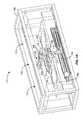
- FIG. 1Ais a simplified perspective illustration of a fluid dispensing apparatus according to one embodiment of the present invention.
- Fluid dispensing apparatus 100is illustrated as containing a frame 105 .
- Additional componentsare provided by embodiments of the present invention, although, for purposes of clarity, not all components are illustrated.
- intake and exhaust ports, as well as electrical feeds generally present at the sides of the frameare not illustrated in FIG. 1A . Additional details concerning some of the components are provided in FIG. 2 .
- processing chambers 110 and 111are located within frame 105 on the left and right sides of a central fluid dispense bank 112 , respectively.
- processing chambers 110 and 111are referred to as processing stations.
- processing stationis used interchangeably.
- the inventionhas been applied to a coater/developer module with a pair of coat/develop bowls horizontally arrayed on either side of a central fluid dispense bank, but this is not required by the present invention.
- the coat moduleis a photoresist module with different photoresists as well as photoresists combined with different concentrations of solvents.
- the fluids dispensed by the central fluid dispense bankmay be delivered in the form of liquid, vapor, mist, or droplets.
- the processing chambersare processing modules that may be adapted to perform, for example, coating processes using organic and inorganic fluids, hybrid organic/inorganic fluids, aqueous fluids, and the like.
- these fluidsmay be utilized in processes including bottom antireflection coating (BARC), resist, top antireflection coating (TARC), develop, shrink coat, PIQTM (Poly-Isoindolo-Quinazolinedione), spin on materials including spin on glass, spin on dielectric, spin on hardmask, and the like.
- processes utilizing other fluidsincluding those used for electroless and electrochemical plating processes, as well as wet clean and the like, are included in the scope of the present invention.
- the processing chambers 110 and 111generally contain all of the processing components described in U.S. Provisional Application Ser. No. 60/639,109 in conjunction with the coater module or developer module. Additionally, the two chambers share central fluid dispense bank 112 .
- the central fluid dispense bankcontains a number of dispense nozzles 114 .
- Each spin chuck 130 and 131is coupled to a motor (not shown) through a shaft (not shown) and adapted to rotate about an axis perpendicular to the face of the spin chuck.
- the spin chucks 130 and 131contain a sealing surface connected to a vacuum source that is adapted to hold the substrate while the substrate is being rotated.
- a controller(not shown) is provided and connected to the motors so that the timing and rotation speed of the spin chucks can be controlled in a predetermined manner.
- the rotation speedmay be variable or constant as a function of time.
- the rotation motoris adapted to rotate a 300 mm semiconductor substrate between about 1 revolution per minute (RPM) and about 5,000 RPMs with an acceleration rate of up to about 50,000 RPMs/s.
- the dispense arm assembly 118is actuated in three dimensions by motors 105 , 106 , and 107 .
- Motor 105is used to move the dispense arm assembly along the guide rail 119 in a first direction, sometimes referred to as a longitudinal direction.
- the motoris selected to provide for motion of the dispense arm assembly with predetermined speed, accuracy, and repeatability.
- the travel of the dispense arm assembly along the guide railis sufficient for the dispense arm assembly to reach the center of both wafers.
- motion stops, positional feedback, and interlocksare provided as are well known to one of skill in the art.
- Motor 106is used to move extension arm 117 in a second (vertical) direction, sometimes referred to as a transverse direction.
- the motoris selected to provide for motion of the extension arm with predetermined speed, accuracy, and repeatability.
- the travel of the extension arm in the transverse directionis sufficient for a gripper assembly to reach the dispense nozzles, and to lift the dispense nozzles above upper edges of the cups, extension arm access doors, and other obstructions while moving to the center of the spin chuck.
- motion stops, positional feedback, and interlocksare provided as are well known to one of skill in the art.
- Motor 107is used to move the gripper assembly 108 in a third direction, sometimes referred to as a lateral direction. As illustrated in FIG. 1A , the gripper assembly 107 is moveable along the extension arm 220 and is shown in a first position above nozzle holder assembly 117 and in a second optional position above nozzle holder assembly 116 .
- the motoris selected to provide for motion of the gripper assembly with predetermined speed, accuracy, and repeatability.
- the travel of the gripper assembly in the lateral directionis sufficient for the gripper assembly to reach both nozzle banks. In embodiments in which a single nozzle bank oriented in the transverse direction is utilized, the travel of the gripper assembly is sufficient for the gripper assembly to reach all nozzles in the bank.
- motion stops, positional feedback, and interlocksare provided as are well known to one of skill in the art.
- FIG. 1Bis a simplified perspective illustration of a fluid dispensing apparatus according to another embodiment of the present invention.
- dispense arm access shutters 122 and 123are provided inside the frame 105 .
- Dispense access arm shutter 122is positioned between the first processing chamber 110 and the central fluid dispense bank 112 .
- Dispense access arm shutter 123is positioned between the central fluid dispense bank and the second processing chamber 111 .
- the dispense arm access shuttersare moveable between an open and closed positioned, along with positioned therebetween.
- dispense arm access shutter 122is about half way between the open and closed position.
- Dispense arm access shutter 123is illustrated in a closed position. When the dispense arm access shutters are in the open position, the dispense arm assembly is free to travel between the processing chambers and the central fluid dispense bank.
- FIG. 2is a simplified schematic plan view of a fluid dispensing apparatus according to one embodiment of the present invention.
- the cups 140 and 141are manufactured from a material characterized by suitable rigidity and solvent-resistance.
- cups 140 and 141are manufactured from a plastic material (e.g., Polytetrafluoroethylene (PTFE), perfluoroalkoxy (PFA) , polypropylene, or Polyvinylidene fluoride (PVDF)), a ceramic material, a metal coated with a plastic material (e.g., aluminum or SST coated with either PVDF, Halar, etc.), or other materials that are compatible with the processing fluids delivered from the fluid dispense system 112 .
- PTFEPolytetrafluoroethylene
- PFAperfluoroalkoxy
- PVDFPolyvinylidene fluoride
- a lift assemblygenerally contains an actuator (not shown), such as an air cylinder or servomotor, and a guide (not shown), such as a linear ball bearing slide, which are adapted to raise and lower the rotatable spin chucks 130 and 131 to a desired position.
- the lift assemblyis thus adapted to position the substrate mounted on the rotatable spin chucks in the cups during processing and also lift the substrate above the top of the cup to exchange the substrate with an external robot positioned outside the enclosure 100 .
- a robot blade(not shown), which is attached to the external robot, enters the apparatus 100 through the robot access shutters 120 and 121 .
- a pre-wet nozzle 115is located at a distal end of extension arm assembly 118 .
- the pre-wet nozzleis plumbed through components coupled to the extension arm.
- the design of each of the individual dispense nozzlesis simplified.
- no pre-wet nozzleis included as part of each dispense nozzle.
- the extension armis a telescoping arm, thus capable of controllably positioning the pre-wet nozzle 115 a desired distance from the guide mechanism 119 .
- backside rinse (BSR) nozzles 138are included on a portion of the bowl situated below a substrate positioned on the spin chucks 130 and 131 .
- the BSR nozzlesprovide a solvent applied to the backside of the substrate during a cleaning step.
- an edge bead removal (EBR) arm 150is provided at a corner of each processing chamber. As illustrate in FIG. 2 , the EBR arm rotates around a pivot 152 located at a proximal end of the EBR arm to position a distal end of the EBR arm at a position over an edge of a substrate mounted on the spin chuck. An EBR fluid is dispensed through a nozzle located at the distal end of the EBR arm to remove an edge bead present on the substrate.
- a gas flow distribution systemis adapted to deliver a uniform flow of a gas through the enclosure 100 and processing chambers 110 and 111 .
- the gas flow distribution systemprovides temperature and/or humidity controlled air through supply ports 160 .
- Cup exhausts 162provide for removal of air from the processing chamber.
- Cup drains 164provide for removal of fluids from the cups.
- four portsare shown in relation to the temperature and/or humidity controlled air, the cup exhausts, and the cup drains. This illustration is provided because, in some embodiments, four dispense systems are vertically stacked to reduce system footprint.
- each of the illustrated cup exhaustsis coupled to a cup in one of the four dispense systems.
- FIG. 2Although the various air and fluid handling components shown in FIG. 2 are illustrated as four separate ports, this is not required by the present invention. In alternative embodiments, the air and fluid handling components are provided in different numbers depending on the overall system architecture. Additionally, although the ports are illustrated as uniform in dimension within each group, this is not required by the present invention. Moreover, combination of separate ports into larger communal ports are provided in alternative embodiments. One of ordinary skill in the art would recognize many variations, modifications, and alternatives.
- provision of temperature and humidity controlled gas, for example, air, to the processing chambersgenerally extends to the monitoring and control of various air flow parameters.
- the environment of the chamberis monitored and parameters including the solvent partial pressure and vapor concentration, air flow velocity, air flow rates, and differential pressure among others, are controlled to achieve the desired air temperature and humidity.
- static discharge from the film present on the substrateis controlled in some embodiments in addition to the chamber environment. Accordingly, through control of the processing chamber environment and substrate parameters, among other factors, such as chuck spin rate, it is possible to control the coating characteristics.
- Each of the two chambersalso includes a robot access shutter 120 / 121 to alternately provide a seal for an access port and provide access for a robot arm to pass through the access port.
- the robot access shutteris opened.
- a robot arm(not shown), on which the substrate is supported, is moved through the access port to move the substrate from a position outside the processing chamber to a position over one of the spin chucks. Utilizing methods well known to one of skill in the art, the robot arm places the substrate on the spin chuck, exits the processing chamber, and the robot access shutter is closed.
- a robotcan load substrates into processing chambers 110 and 111 independently in an alternating manner.
- robot access shutter 121is opened to load a substrate into processing chamber 111 .
- robot access shutter 120provides independent access to processing chamber 110 .
- System throughputis enhanced using embodiments of the present invention as loading and processing of substrates is performed simultaneously in the two processing chambers.
- each of the two processing chambersalso include a dispense arm access shutter 122 and 123 positioned between the spin chucks 130 and 131 , respectively, and the central fluid dispense bank 112 .
- dispense arm access shuttersare not provided in the embodiment illustrated in FIG. 1 , in some embodiments, the dispense arm access shutters provide a shield to isolate the processing chambers from the central fluid dispense bank during operation of the system.
- the dispense arm access shutteris opened to permit movement of a dispense arm assembly 118 into the processing chambers and closed after completion of the dispense step and return of the dispense arm assembly to the central fluid dispense bank region.
- coat processesinclude accelerating the substrate to a desired spin rate, dispensing the coating fluid, e.g., resist, for several seconds, and continue spinning the substrate for tens of seconds.
- the substrateis spun up until a rate of 500 RPMs is reached, resist is dispensed for about 3 seconds, and the substrate is maintained at a spin rate of 1,800 RPMs for about 60 seconds.
- the dispense armreturns to the central fluid dispense bank and the dispense arm access shutter is closed while the substrate continues spinning for about 55 seconds.
- the dispense arm access shutters 122 and 123not only provide for isolation from liquids present in the central fluid dispense bank, but for additional particle control inside each of the processing chambers.
- the dispense arm access shutterprovides a seal for the processing chamber that limits the flow of air-borne particles from the central fluid dispense bank into the processing chambers. Accordingly, the dispense arm access shutters minimize cross-talk between processing chambers and prevent contaminants from traveling across chamber boundaries. Additionally, the dispense arm access shutters provide for substantial flow restriction between processing chambers, reducing the air flow between the respective processing chambers and the central fluid dispense bank.
- the dispense arm access shuttersare made from chemically resistant materials such as aluminum and the like.
- the dispense arm access shuttersare moved between various positions in linear, rotary, angled trajectories, or the like.
- the dispense arm access shuttersare actuated by pneumatic pressure, a solenoid, or by a motor, depending on the particular application.
- the motion of the dispense arm access shuttersis controlled in conjunction with one or more interlocks.
- the interlocksoperate using mechanical, electrical, or software switches or controls.
- embodiments of the present inventionindependent control of the temperature and/or humidity in the vicinity of each of the substrates.
- the parameters associated with the finished coatingare a function of the temperature of the coating process, the humidity in the vicinity of the substrate, or both.
- Embodiments of the present inventionprovide for independent temperature and/or humidity control in processing chambers 110 and 111 .
- embodiments of the present inventionprovide the necessary control.
- a coating processmay require control over the temperature and the humidity of the environment surrounding the substrate being coated, while simultaneously, a develop process may only require control of the temperature.
- either the temperature, the humidity, or bothmay be independently controlled in the two processing chambers.
- the temperature and/or humidity inside a processing chambermay be controlled prior to, during, and after a dispense operation by the use of the robot arm access doors.
- the access doorcan be opened to admit the dispense arm, partially closed during the fluid dispense step, fully re-opened to enable the dispense arm to exit the processing chamber, and fully closed during the completion of the dispense process.
- the central fluid dispense bank 112contains a plurality of nozzles 114 that are contained in one or more nozzle holder assemblies 116 .
- the fluid dispense system used in the coater or developer modulesmay contain one or more fluid source assemblies (not shown) which deliver one or more processing fluids to the surface of a substrate mounted on the spin chuck 130 .
- the home position of the dispense armis in the central fluid dispense bank region.
- the dispense armis located at the home position in the central fluid dispense bank region.
- each nozzle 114contained in the nozzle holder assemblies 116 , is typically connected to plumbing components (including a supply tube, a pump, a filter, a suck back valve, a fluid source, and the like) and is adapted to dispense a single type of processing fluid.
- the processing fluidis a photoresist, a solvent, a coating, a developer, or the like.
- each central fluid dispense bankcan serve both processing chambers, thus reducing the redundancy required in each processing chamber.
- a resist nozzle banktypically includes between four and ten nozzles.
- a resist nozzle bankincludes more than ten nozzles.
- resist nozzlesare adapted to dispense a variety of chemicals, including resist, antireflection coatings, and spin on materials (e.g., SOG and SOD).
- a develop nozzle banktypically includes between one and three nozzles. In some embodiments, more than three develop nozzles are included in a develop nozzle bank. Additionally, some develop nozzle banks include a number of rinse lines as appropriate to the particular application.
- embodiments of the present inventionprovide central fluid dispense banks with nozzles appropriate to the function of the particular dispense assembly.
- the central fluid dispense bankincludes a number of dispense nozzles.
- the dispense nozzlesare arranged in two groups of nozzles, specifically, a first group of five nozzles contained in nozzle holder assembly 116 and a second group of five nozzles contained in nozzle holder assembly 17 .
- the dispense nozzlesare arrayed longitudinally in the nozzle holder assemblies. In other words, the long dimension of the nozzle holder assemblies is aligned parallel to a line connecting the center of spin chuck 130 with the center of spin chuck 131 .
- the nozzle holder assembliesare aligned parallel to a line connecting the center of the first processing chamber and the second processing chamber.
- Another frame of reference to which the nozzle holder assemblies can be referencedis the length of the guide mechanism 119 .
- the nozzle holder assemblies 116 and 117are aligned parallel to the length of the guide mechanism 119 .
- FIGS. 1-3illustrate a configuration where each nozzle holder assembly 116 contains five nozzles 114
- the nozzle holder assembly 116may contain a lesser number of nozzles or a greater number of nozzles without varying form the basic scope of the invention.
- two banks containing eight nozzles per bankare provided.
- the nozzle holder assembliesare illustrated as aligned parallel to the length guide mechanism 119 in FIG. 1 , this is not required by the present invention.
- the nozzle holder assembliesare aligned perpendicular to the length of the guide mechanism.
- a single bank containing eight nozzlesis provided.
- the single nozzle bankis arranged with nozzle holder assembly aligned perpendicular to the length of the guide mechanism.
- all of the dispense nozzles provided in the nozzle dispense banksare arrayed in a single plane parallel to the plane including the spin chucks.
- the dispense nozzlesare stacked vertically, with a first number of nozzles arrayed in a first plane and a second number of nozzles are arrayed in a second plane.
- the nozzlesare both stacked vertically and staggered laterally, providing access to the nozzles are appropriate to a particular application.
- FIG. 3Ais a simplified schematic plan view of a fluid dispensing apparatus in a first mode of operation according to one embodiment of the present invention.
- the fluid dispensing apparatusis a coater/developer module in a specific embodiment of the present invention.
- the dispense arm assembly 118is positioned over the right processing chamber to dispense a processing fluid onto a substrate 210 retained on the spin chuck 130 .
- the dispense arm assembly 118may contain an arm 220 and nozzle holding mechanism 222 .
- the dispense arm assembly 118is attached to an actuator 224 that is adapted to transfer and position the dispense arm assembly 118 in any position along the guide mechanism 226 .
- a system controller(not shown) is adapted to move the dispense arm assembly 118 vertically to correctly position the nozzle 114 over the substrate 210 during processing and also enable the nozzle holding mechanism to pick-up and drop-off the nozzles 114 from the nozzle holder assemblies 116 .
- dispense arm access shutter 123is adapted to move vertically to close and isolate one processing chamber 111 during processing from the central fluid dispense bank 112 along with the other process module 110 to prevent cross contamination of the substrates during processing.
- FIG. 3Bis a simplified schematic plan view of a fluid dispensing apparatus in a second mode of operation according to another embodiment of the present invention.
- the dispense arm assembly 118is positioned over the left processing chamber 110 to dispense a processing fluid on a substrate 310 retained on the spin chuck 130 .
- Dispense arm access shutter 122is adapted to move vertically to close and isolate processing chamber 110 from the central fluid dispense bank 112 along with the other processing chamber 111 during processing to prevent cross contamination of the substrates during processing.
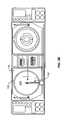
- FIG. 6is a simplified schematic plan view of a fluid dispensing apparatus according to another embodiment of the present invention.
- the fluid dispensing apparatusshares some commonalities with the apparatus illustrated in FIG. 2 .
- the apparatus illustrated in FIG. 6includes a central fluid dispense bank 612 comprising a number of dispense nozzles, a home region 614 and two processing chambers positioned on opposite sides of the central fluid dispense bank and home region.
- the central fluid dispense bankcontains a single nozzle holder assembly 616 with the long dimension of the nozzle holder assembly substantially perpendicular to a line connecting the center of processing chamber 610 and the center of processing chamber 611 .
- the assembly illustrated in FIG. 6also contains two nozzle arm assemblies 620 and 622 which are adapted to access, select, and detachably couple a dispense nozzle 618 from the nozzle holder assembly contained in the shared central fluid dispense bank.
- Each dispense arm assemblyis actuated by motors (not shown) to translate the selected dispense nozzle to a desired position over the surface of the associated substrate.
- dispense arm assembly 620is associated with spin chuck 630 and dispense arm assembly 622 is associated with spin chuck 632 .
- dispense arm assembly 622is located at the home region and is not coupled to a dispense nozzle.
- dispense arm assembly 620is coupled to a dispense nozzle, which was initially positioned at location 640 in the nozzle holder assembly. Additionally, dispense arm assembly 620 has been moved to a position from which a coating fluid dispensed from the dispense nozzle will impinge on the center of substrate 650 .
- the dispense arm access shuttershave been subdivided in the embodiment illustrated in FIG. 6 to provide separate access for the dispense arm assemblies with respect to the home position and the central fluid dispense bank. Additional moveable or permanent partitions are included in additional embodiments as will be evident to one of skill in the art. Merely by way of example, a permanent partition 660 located between the central fluid dispense bank 612 and the home position 614 will provide for environmental isolation between the central fluid dispense bank and the home region. In the embodiment illustrated in FIG. 6 , each of the dispense nozzles may be plumbed to provide a different fluid solution. Alternatively, multiple nozzles may share the same pump and dispense the same fluid, for example a particular resist. Accordingly, the fluid dispensing apparatus illustrated in FIG. 6 is capable of performing a wide variety of coat and develop processes.
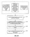
- FIG. 4Ais a simplified flowchart illustrating a method of operating a fluid dispense apparatus according to one embodiment of the present invention.
- the methodincludes providing a central fluid dispense bank comprising a number of dispense nozzles in step 410 .
- the central fluid dispense bankcontains 16 nozzles providing 16 different resists.
- 16 nozzlesare provided, but a single resist is provided by each nozzle, with the concentration of solvent varying with each nozzle.
- the central fluid dispense bankcontains a lesser or greater number of nozzles, depending on the particular application.
- the methodalso includes (step 412 ) providing a first processing chamber positioned on a first side of the central fluid dispense bank and a second processing chamber positioned on a second side of the central fluid dispense bank, wherein the first side is opposite the second side.
- the methodfurther includes providing a dispense arm assembly located at a home position in step 414 .
- the home positionis in the central fluid dispense bank region and the dispense arm assembly is adapted to translate between the central fluid dispense bank and the first and second processing chambers.
- the home positionis not limited to a particular location inside the central fluid dispense bank region, but is understood to be a general location in the vicinity of the dispense nozzles.
- a dispense nozzleis selected from the dispense nozzles located in the central fluid dispense bank and the selected nozzle is coupled to the dispense arm assembly.
- the step of selecting a first dispense nozzleincludes detachably coupling the nozzle to the dispense arm using a gripper assembly integrated into an extension arm of the dispense arm assembly.
- the dispense arm assemblyis adapted to move in three dimensions, enabling the dispense arm assembly to lift the selected nozzle out of the nozzle holder assemblies and move the nozzle to either of the processing chambers.
- step 418the dispense arm assembly is translated by actuation of motors coupled to the dispense arm assembly. The dispense arm assembly is moved to position the dispense nozzle at a first position in the first processing chamber.
- the methodincludes positioning the nozzle at a first dispense position located over the center region of the substrate mounted on spin chuck 130 , but this is not required by the present invention. Alternative embodiments utilize other positions within processing chamber 110 .
- the spin chuckis rotated to bring the substrate rotational speed to a predetermined value.
- the spin chuckaccelerates the substrate with an acceleration rate of up to about 50,000 RPMs/s to bring the substrate from a stationary position to a rotation rate of about 5,000 RPMs.
- the acceleration rateranges from about 10 RPMs/s to about 50,000 RPMs/s and the rotation rate ranges from about one RPM to about 5,000 RPMs.
- the acceleration rate and the rotation ratewill depend upon the particular applications.
- the first positionis selected to position the solvent pre-wet nozzle present on the dispense arm assembly at a dispense position.
- the dispense positionis one in which the solvent pre-wet nozzle is positioned over the center of the substrate. After the solvent pre-wet nozzle is positioned, solvent is dispensed onto the spinning substrate. Subsequently, the dispense arm assembly is actuated to move the dispense arm assembly and position the dispense nozzle over the center of the substrate prior to dispensing fluid from the dispense nozzle.
- a coating fluidis dispensed from the selected dispense nozzle, generally on a center portion of the substrate mounted on spin chuck 130 in step 420 .
- the spin chuckis rotated during the dispense operation to spread the coating fluid over the surface of the substrate.
- the rotation speedmay be variable or constant as a function of time.
- the dispense armis returned to the home position in step 422 and selected dispense nozzle is returned to the central fluid dispense bank.
- FIG. 4Bis a simplified flowchart illustrating a method of operating a fluid dispense apparatus according to another embodiment of the present invention. Steps 450 through 460 in FIG. 4B parallel steps 410 through 420 in FIG. 4A . In the alternative embodiment illustrated in FIG. 4B , rather than returning the dispense arm assembly to the central fluid dispense bank and returning the selected dispense nozzle to the central fluid dispense bank, the dispense arm assembly is translated to a second position located over the center region of a second substrate mounted on spin chuck 131 in step 462 .
- the second positionis selected to allow for dispensing of a solvent onto the center of the second substrate prior to adjustment of the dispense nozzle position and dispensing of the coating fluid from the dispense nozzle.
- the spin chuck 131is rotated to bring the substrate rotational speed to a predetermined value.
- the dispense parametersmay be the same or different from those employed during the first dispense step.
- the optional solvent pre-wet and the coating fluidare dispensed from the selected dispense nozzle in step 464 , generally on a center portion of the substrate mounted on spin chuck 131 .
- the spin chuckis rotated during the dispense operation to spread the coating fluid over the surface of the substrate.
- the rotation speedmay be variable or constant as a function of time.
- the dispense arm assemblyis returned to the home position over the central fluid dispense bank in step 466 and the selected dispense nozzle is returned to the central fluid dispense bank.
- stepsare inserted between steps 460 and 462 so that a first dispense nozzle is selected for the first dispense step and a second dispense nozzle is selected for the second dispense step.
- the method of dispensing fluid onto substratesis not stopped after the second dispense step, but continued for more than two dispense steps.
- the dispense stepsmay alternate between processing chambers or may feature multiple sequential dispense steps in one processing chamber with the same or a different coating fluid. The variations possible with multiple dispense nozzles, multiple processing chambers and a home position for the dispense arm assembly in the central fluid dispense bank region will be apparent to one of skill in the art.
- Substratescan be loaded into the two processing chambers using any appropriate robot.
- a central robotis adapted to transfer substrates into and out of both processing chambers in an alternating manner in one embodiment of the present invention.
- the dispense arm assemblyis positioned at a home position in the central fluid dispense bank region while the substrates are loaded by the central robot into the processing chambers.
- the dispense arm access doorsare generally kept closed to limit movement of air and air-borne particles between the processing chambers and the central fluid dispense bank region.
- the above sequence of stepsprovides a method for dispensing a fluid onto a semiconductor substrate according to an embodiment of the present invention. As shown, the method uses a combination of steps including a way of utilizing a central fluid dispense bank shared by two processing chambers according to an embodiment of the present invention. Other alternatives can also be provided where steps are added, one or more steps are removed, or one or more steps are provided in a different sequence without departing from the scope of the claims herein. Further details of the present method can be found throughout the present specification.
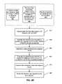
- FIG. 5is a simplified flowchart illustrating a method of operating a fluid dispense apparatus according to yet another embodiment of the present invention.
- the methodincludes providing a central fluid dispense bank in step 510 .
- the central fluid dispense bankcomprises a number of dispense nozzles.
- the central fluid dispense bankcontains 16 nozzles providing 16 different resists.
- 16 nozzlesare provided, but a single resist is provided by each nozzle, with the concentration of solvent varying with each nozzle.
- the central fluid dispense bankcontains a lesser or greater number of nozzles, depending on the particular application.
- the methodalso includes providing a first processing chamber positioned on a first side of the central fluid dispense bank (step 512 ) and a second processing chamber positioned on a second side of the central fluid dispense bank (step 514 ).
- the first processing chamber and the second processing chamberare positioned on opposite sides of the central fluid dispense bank.
- the methodfurther includes providing a dispense arm assembly at a home position (step 516 ) that is adapted to translate between the central fluid dispense bank and the first and second processing chambers and selecting a dispense nozzle from the plurality of dispense nozzles.
- the step of selecting the dispense nozzleincludes detachably coupling the nozzle to the dispense arm assembly using a gripper assembly integrated into an extension arm of the dispense arm assembly (step 518 ).
- the gripper assemblyis translated in the vertical and lateral directions after coupling the nozzle to the gripper assembly.
- Translation in the vertical directionis utilized in one embodiment to separate tubing coupled to the selected dispense nozzle from tubing coupled to other dispense nozzles in the nozzle holder assembly, reducing particle counts.
- One of ordinary skill in the artwould recognize many variations, modifications, and alternatives.
- the first processing chamber and the second processing chamberare controlled to provide separate temperature and humidity environments for each of the processing chambers.
- dispense arm access shuttersare provided between the central fluid dispense bank and both of the processing chambers, thereby providing environmental control for the processing chambers.
- a first dispense arm access shutter located between the central fluid dispense bank and the first processing chamberis opened. The opening of the first dispense arm access shutter provides a path for the dispense arm assembly to move the selected nozzle from the central fluid dispense bank to a first position in the first processing chamber (step 522 ).
- the first dispense positionis a position at which the dispense nozzle is located over the center region of the substrate mounted on spin chuck 130 , but this is not required by the present invention.
- Alternative embodimentsutilize other positions within processing chamber 110 , for example, a position in which the solvent pre-wet nozzle is positioned over the center of the substrate.
- the spin chuckis rotated to bring the substrate rotational speed to a predetermined value.
- the spin chuckaccelerates the substrate with an acceleration rate of up to about 50,000 RPMs/s to bring the substrate from a stationary position to a rotation rate of about 5,000 RPMs.
- the acceleration rateranges from about 10 RPMs/s to about 50,000 RPMs/s and the rotation rate ranges from about one RPM to about 5,000 RPMs.
- the acceleration rate and the rotation ratewill depend upon the particular applications.
- a coating fluidis dispensed from the dispense nozzle in step 524 , generally on a center portion of the substrate mounted on spin chuck 130 .
- the spin chuckis rotated during the dispense operation to spread the coating fluid over the surface of the substrate.
- the rotation speedmay be variable or constant as a function of time.
- the dispense arm assemblyis translated to the home position.
- the time period during which the substrate is rotated after fluid dispenseis less than the translation time for the dispense arm assembly to move from the dispense position to the central fluid dispense bank region.
- the dispense arm assemblyexits the first processing chamber after the dispense step and the first dispense arm access shutter is closed prior to the completion of the spin step.
- a second dispense arm access shutterlocated between the central fluid dispense bank and the second processing chamber is opened.
- the opening of the second dispense arm access shutterprovides a path for the dispense arm assembly to move the selected nozzle from the central fluid dispense bank to a second position in the second processing chamber (step 532 ).
- the second dispense positionis a position at which the dispense nozzle is located over the center region of the substrate mounted on spin chuck 131 , but this is not required by the present invention.
- Alternative embodimentsutilize other positions within processing chamber 111 , for example, a position in which the solvent pre-wet nozzle is positioned over the center of the substrate.
- the spin chuck 131is rotated to bring the substrate rotational speed to a predetermined value.
- a coating fluidis dispensed from the dispense nozzle in step 534 , generally on a center portion of the substrate mounted on spin chuck 131 .
- the spin chuckis rotated during the dispense operation to spread the coating fluid over the surface of the substrate.
- the rotation speedmay be variable or constant as a function of time.
- the dispense arm assemblyis translated to the home position. In a particular embodiment, the time period during which the substrate is rotated after fluid dispense is less than the translation time for the dispense arm assembly to move from the dispense position to the central fluid dispense bank region.
- the dispense arm assemblyexits the second processing chamber after the dispense step and the second dispense arm access shutter is closed (step 538 ) prior to the completion of the spin step.
- the selected dispense nozzleis detached from the dispense arm assembly in step 540 .
- the above sequence of stepsprovides a method for dispensing a fluid onto a number of semiconductor substrates according to an embodiment of the present invention. As shown, the method uses a combination of steps including a way of utilizing a central fluid dispense bank shared by two environmentally controlled processing chambers according to an embodiment of the present invention. Other alternatives can also be provided where steps are added, one or more steps are removed, or one or more steps are provided in a different sequence without departing from the scope of the claims herein. Further details of the present method can be found throughout the present specification.
- the dispense arm access shutteris opened, partially closed, and reopened during each coating process.
- the dispense arm access shutteris partially closed after the dispense arm enters the processing chamber and the dispense arm is moved to the side of the processing chamber adjacent the central fluid dispense bank after the fluid is dispensed.
- the dispense arm access shutterremains partially closed during the coating process while the dispense arm waits at the side of the processing chamber for the coating process to be completed.
- the dispense arm access shutteris opened, the dispense arm returns to the central fluid dispense bank region, where the first dispense nozzle is returned to the central fluid dispense bank, and the dispense arm access shutter is closed once again.
- the time during which the dispense arm access shutter is open and the processing chamber is exposed to the environment of the central fluid dispense bank regionis minimized, reducing cross contamination from either the central fluid dispense bank or the other processing chamber.
- stepsare inserted between steps 528 and 530 so that a first dispense nozzle is selected for the first dispense step and a second dispense nozzle is selected for the second dispense step.
- the method of dispensing fluid onto substratesis not stopped after the second dispense step, but continued for more than two dispense steps.
- the dispense stepsmay alternate between processing chambers or may feature multiple sequential dispense steps in one processing chamber with the same or a different coating fluid. The variations possible with multiple dispense nozzles, multiple processing chambers and a home position for the dispense arm assembly in the central fluid dispense bank region will be apparent to one of skill in the art.
- FIG. 8is a simplified timing diagram illustrating operation of a fluid dispensing apparatus according to one embodiment of the present invention. This diagram is merely an example of a process flow, which should not limit the scope of the claims herein. Moreover, the diagrams presented in FIG. 8 are not drawn to scale, but merely represent a series of timed events in relation to each other.
- FIG. 8Aillustrates the motion of the dispense arm assembly along the guide rail 119 as illustrated in FIG. 2 . With reference to FIGS.
- the motion of the dispense arm assembly to the left (to service processing chamber 110 ) and to the right (to service processing chamber 111is illustrated by plotting the velocity of the dispense arm assembly in the left and right directions as a function of time as a positive and negative velocity, respectively.
- the dispense arm assemblyis translated from the home position to the left for a predetermined time period and stopped.
- the predetermined time period and the velocity of motionare related as will be evident to one of skill in the art.
- the motion of the dispense arm assembly and dispense nozzles in the vertical direction (with respect to FIG. 2 ) and the direction perpendicular to the guide rail in the plane of the figureare not illustrated in FIG. 8A for purposes of clarity, but one of skill in the art will appreciate that these motions are included as discussed previously.
- the spin rate of the spin chuck in processing chamber 110(PC 1 ) is illustrated as a function of time.
- the spinning of the chuck in processing chamber 110is not initiated until the dispense arm assembly is located at a desired position and stopped.
- the spin processis begun while the dispense arm assembly is still in a state of motion.
- the dispense arm assemblyis moved in some embodiments, from a first position in which solvent for a pre-wet process is dispensed to a second position in which a resist or other fluid is dispensed. In the embodiment illustrated in FIG.
- the spin process for the spin chuck in processing chamber 110is initiated at time t 1 , before the motion of the dispense arm assembly has been stopped.
- the spin chuckis accelerated, maintained at a constant rotational velocity R 1 for a first predetermined time during the dispense process, and accelerated to a second, higher rotational velocity R 2 for a second predetermined time period.
- R 1rotational velocity
- R 2rotational velocity
- FIG. 8Cillustrates the volume of fluid dispensed from the dispense nozzle as a function of time.
- FIGS. 8A and 8Cillustrate that the dispense arm assembly is positioned in processing chamber 110 (PC 1 ) during this dispense step.
- the fluid dispense stepis performed while the spin chuck in processing chamber 110 is spinning at the first rate, R 1 .
- additional dispense stepssuch as solvent pre-wet, have been omitted from this figure.
- the volume of fluid dispensedis illustrated as constant as a function of time during the fluid dispense step, one of skill in the art will appreciate that this is not required by the present invention.
- the volume dispensed as a function of timefollows other functional relationships, for example, increasing and/or decreasing the dispensed volume as a function of time as appropriate to a particular process.
- FIGS. 8D and 8Eillustrated the spin rate of the spin chuck in processing chamber 111 (PC 2 ) and the volume of fluid dispensed from the dispense nozzle as functions of time.
- the dispense arm assemblyis translated from the left processing chamber 110 in the right direction, moving the dispense nozzle to a desired position in processing chamber 111 .
- the time utilized to move the dispense arm assembly from processing chamber 110 to processing chamber 111is greater than the time originally required to move the dispense arm assembly from the home position to processing chamber 111 . In some embodiments, this increased time results from the motion of the dispense arm assembly at a generally equal speed, but traveling over a greater distance.
- velocities, distances, and timesare related as will be evident to one of skill in the art.
- the translation of the dispense arm assembly illustrated in FIG. 8A at time t 3is shown as occurring at a constant velocity.
- the motion of the dispense arm assemblyis stopped at the home position, the dispense nozzle is changed as discussed above, and the motion continues in the left direction.
- One of ordinary skill in the artwould recognize many variations, modifications, and alternatives.
- the spin chuck in processing chamber 111is spun up to first rotational velocity R 3 at time t 4 and the rotational velocity is further increased to velocity R 4 after the fluid is dispensed at time t 5 .
- the spin processes in the two processing chambersare overlapped.
- the use of a shared dispense architectureresults in improved system throughput, among other advantages.
- the dispense arm assemblyis translated to the home position at time t 6 .
Landscapes
- Engineering & Computer Science (AREA)
- General Physics & Mathematics (AREA)
- Physics & Mathematics (AREA)
- Manufacturing & Machinery (AREA)
- Microelectronics & Electronic Packaging (AREA)
- Power Engineering (AREA)
- Computer Hardware Design (AREA)
- Condensed Matter Physics & Semiconductors (AREA)
- Robotics (AREA)
- General Engineering & Computer Science (AREA)
- Quality & Reliability (AREA)
- Automation & Control Theory (AREA)
- Container, Conveyance, Adherence, Positioning, Of Wafer (AREA)
- Coating Apparatus (AREA)
- Exposure Of Semiconductors, Excluding Electron Or Ion Beam Exposure (AREA)
- Exposure And Positioning Against Photoresist Photosensitive Materials (AREA)
- Manipulator (AREA)
- Photosensitive Polymer And Photoresist Processing (AREA)
- Materials For Photolithography (AREA)
Abstract
Description
- Application Ser. No. 11/111,353, filed Apr. 20, 2005, entitled “Coat/Develop Module with Shared Dispense”;
- Application Ser. No. 11/111,154, filed Apr. 20 2005, entitled “Coat/Develop Module with Independent Stations”.
Claims (13)
Priority Applications (5)
| Application Number | Priority Date | Filing Date | Title |
|---|---|---|---|
| US11/111,154US7255747B2 (en) | 2004-12-22 | 2005-04-20 | Coat/develop module with independent stations |
| PCT/US2005/046906WO2006069348A2 (en) | 2004-12-22 | 2005-12-21 | Coat/develop module with shared dispense |
| KR1020077016731AKR100925898B1 (en) | 2004-12-22 | 2005-12-21 | Coat/develop module with shared dispense |
| JP2007548557AJP4842280B2 (en) | 2004-12-22 | 2005-12-21 | Coat / development module with shared distribution |
| JP2011006873AJP4768084B2 (en) | 2004-12-22 | 2011-01-17 | Coat / development module with shared distribution |
Applications Claiming Priority (2)
| Application Number | Priority Date | Filing Date | Title |
|---|---|---|---|
| US63910904P | 2004-12-22 | 2004-12-22 | |
| US11/111,154US7255747B2 (en) | 2004-12-22 | 2005-04-20 | Coat/develop module with independent stations |
Publications (2)
| Publication Number | Publication Date |
|---|---|
| US20060134340A1 US20060134340A1 (en) | 2006-06-22 |
| US7255747B2true US7255747B2 (en) | 2007-08-14 |
Family
ID=39193608
Family Applications (18)
| Application Number | Title | Priority Date | Filing Date |
|---|---|---|---|
| US11/111,154Expired - LifetimeUS7255747B2 (en) | 2004-12-22 | 2005-04-20 | Coat/develop module with independent stations |
| US11/111,156Expired - LifetimeUS7371022B2 (en) | 2004-12-22 | 2005-04-20 | Developer endpoint detection in a track lithography system |
| US11/111,155AbandonedUS20060130767A1 (en) | 2004-12-22 | 2005-04-20 | Purged vacuum chuck with proximity pins |
| US11/111,353Active2026-03-10US7396412B2 (en) | 2004-12-22 | 2005-04-20 | Coat/develop module with shared dispense |
| US11/112,932AbandonedUS20060134330A1 (en) | 2004-12-22 | 2005-04-22 | Cluster tool architecture for processing a substrate |
| US11/112,281Expired - LifetimeUS7357842B2 (en) | 2004-12-22 | 2005-04-22 | Cluster tool architecture for processing a substrate |
| US11/147,037AbandonedUS20060134536A1 (en) | 2004-12-22 | 2005-06-06 | Method and system for determining post exposure bake endpoint |
| US11/316,329AbandonedUS20060158240A1 (en) | 2004-12-22 | 2005-12-21 | Distributed temperature control system for point of dispense temperature control on track systems utilizing mixing of hot and cold streams |
| US11/458,667Expired - Fee RelatedUS7925377B2 (en) | 2004-12-22 | 2006-07-19 | Cluster tool architecture for processing a substrate |
| US11/458,664Expired - LifetimeUS7694647B2 (en) | 2004-12-22 | 2006-07-19 | Cluster tool architecture for processing a substrate |
| US12/033,837AbandonedUS20080223293A1 (en) | 2004-12-22 | 2008-02-19 | Cluster tool architecture for processing a substrate |
| US12/106,824Expired - LifetimeUS7743728B2 (en) | 2004-12-22 | 2008-04-21 | Cluster tool architecture for processing a substrate |
| US12/136,006AbandonedUS20080296316A1 (en) | 2004-12-22 | 2008-06-09 | Coat/develop module with shared dispense |
| US12/254,778Expired - Fee RelatedUS8146530B2 (en) | 2004-12-22 | 2008-10-20 | Cluster tool architecture for processing a substrate |
| US12/254,784Expired - Fee RelatedUS8215262B2 (en) | 2004-12-22 | 2008-10-20 | Cluster tool architecture for processing a substrate |
| US12/254,750Expired - Fee RelatedUS8181596B2 (en) | 2004-12-22 | 2008-10-20 | Cluster tool architecture for processing a substrate |
| US13/411,120AbandonedUS20120180983A1 (en) | 2004-12-22 | 2012-03-02 | Cluster tool architecture for processing a substrate |
| US13/524,854Expired - LifetimeUS8550031B2 (en) | 2004-12-22 | 2012-06-15 | Cluster tool architecture for processing a substrate |
Family Applications After (17)
| Application Number | Title | Priority Date | Filing Date |
|---|---|---|---|
| US11/111,156Expired - LifetimeUS7371022B2 (en) | 2004-12-22 | 2005-04-20 | Developer endpoint detection in a track lithography system |
| US11/111,155AbandonedUS20060130767A1 (en) | 2004-12-22 | 2005-04-20 | Purged vacuum chuck with proximity pins |
| US11/111,353Active2026-03-10US7396412B2 (en) | 2004-12-22 | 2005-04-20 | Coat/develop module with shared dispense |
| US11/112,932AbandonedUS20060134330A1 (en) | 2004-12-22 | 2005-04-22 | Cluster tool architecture for processing a substrate |
| US11/112,281Expired - LifetimeUS7357842B2 (en) | 2004-12-22 | 2005-04-22 | Cluster tool architecture for processing a substrate |
| US11/147,037AbandonedUS20060134536A1 (en) | 2004-12-22 | 2005-06-06 | Method and system for determining post exposure bake endpoint |
| US11/316,329AbandonedUS20060158240A1 (en) | 2004-12-22 | 2005-12-21 | Distributed temperature control system for point of dispense temperature control on track systems utilizing mixing of hot and cold streams |
| US11/458,667Expired - Fee RelatedUS7925377B2 (en) | 2004-12-22 | 2006-07-19 | Cluster tool architecture for processing a substrate |
| US11/458,664Expired - LifetimeUS7694647B2 (en) | 2004-12-22 | 2006-07-19 | Cluster tool architecture for processing a substrate |
| US12/033,837AbandonedUS20080223293A1 (en) | 2004-12-22 | 2008-02-19 | Cluster tool architecture for processing a substrate |
| US12/106,824Expired - LifetimeUS7743728B2 (en) | 2004-12-22 | 2008-04-21 | Cluster tool architecture for processing a substrate |
| US12/136,006AbandonedUS20080296316A1 (en) | 2004-12-22 | 2008-06-09 | Coat/develop module with shared dispense |
| US12/254,778Expired - Fee RelatedUS8146530B2 (en) | 2004-12-22 | 2008-10-20 | Cluster tool architecture for processing a substrate |
| US12/254,784Expired - Fee RelatedUS8215262B2 (en) | 2004-12-22 | 2008-10-20 | Cluster tool architecture for processing a substrate |
| US12/254,750Expired - Fee RelatedUS8181596B2 (en) | 2004-12-22 | 2008-10-20 | Cluster tool architecture for processing a substrate |
| US13/411,120AbandonedUS20120180983A1 (en) | 2004-12-22 | 2012-03-02 | Cluster tool architecture for processing a substrate |
| US13/524,854Expired - LifetimeUS8550031B2 (en) | 2004-12-22 | 2012-06-15 | Cluster tool architecture for processing a substrate |
Country Status (3)
| Country | Link |
|---|---|
| US (18) | US7255747B2 (en) |
| JP (3) | JP2012069957A (en) |
| CN (2) | CN101443131B (en) |
Cited By (7)
| Publication number | Priority date | Publication date | Assignee | Title |
|---|---|---|---|---|
| US20060130747A1 (en)* | 2004-12-22 | 2006-06-22 | Applied Materials, Inc. | Coat/develop module with shared dispense |
| US20080070164A1 (en)* | 2006-09-15 | 2008-03-20 | Tokyo Electron Limited | Wet-processing apparatus, wet-processing method and storage medium |
| US20080304940A1 (en)* | 2007-06-06 | 2008-12-11 | Auer-Jongepier Suzan L | Integrated post-exposure bake track |
| US7699021B2 (en) | 2004-12-22 | 2010-04-20 | Sokudo Co., Ltd. | Cluster tool substrate throughput optimization |
| US8911193B2 (en) | 2004-12-22 | 2014-12-16 | Applied Materials, Inc. | Substrate processing sequence in a cartesian robot cluster tool |
| US20210402425A1 (en)* | 2020-06-26 | 2021-12-30 | Armstrong World Industries, Inc. | Coating humidification system |
| US20220339665A1 (en)* | 2019-09-30 | 2022-10-27 | Dürr Systems Ag | Treatment system and treatment method |
Families Citing this family (642)
| Publication number | Priority date | Publication date | Assignee | Title |
|---|---|---|---|---|
| US7474752B2 (en)* | 2003-09-16 | 2009-01-06 | Koninklijke Philips Electronics N.V. | Audio frequency range adaptation |
| JP4271095B2 (en)* | 2004-07-15 | 2009-06-03 | 東京エレクトロン株式会社 | Substrate heating apparatus and substrate heating method |
| JP4426403B2 (en)* | 2004-08-31 | 2010-03-03 | 東京エレクトロン株式会社 | Laser processing equipment |
| JP5154006B2 (en)* | 2004-12-06 | 2013-02-27 | 株式会社Sokudo | Substrate processing equipment |
| US7819079B2 (en)* | 2004-12-22 | 2010-10-26 | Applied Materials, Inc. | Cartesian cluster tool configuration for lithography type processes |
| US20070295276A1 (en)* | 2004-12-22 | 2007-12-27 | Sokudo Co., Ltd. | Bake plate having engageable thermal mass |
| JP4955977B2 (en)* | 2005-01-21 | 2012-06-20 | 東京エレクトロン株式会社 | Coating and developing apparatus and method thereof |
| US20060162658A1 (en)* | 2005-01-27 | 2006-07-27 | Applied Materials, Inc. | Ruthenium layer deposition apparatus and method |
| US20060236941A1 (en)* | 2005-04-20 | 2006-10-26 | Applied Materials, Inc. | Passive wafer support for particle free wafer acceleration |
| US20150227136A1 (en)* | 2005-06-18 | 2015-08-13 | Fred Flitsch | Methods and apparatus for vertically orienting substrate processing tools in a clean space |
| US7513822B2 (en)* | 2005-06-18 | 2009-04-07 | Flitsch Frederick A | Method and apparatus for a cleanspace fabricator |
| US9457442B2 (en)* | 2005-06-18 | 2016-10-04 | Futrfab, Inc. | Method and apparatus to support process tool modules in a cleanspace fabricator |
| EP1912592A4 (en)* | 2005-07-26 | 2016-01-06 | Rox Medical Inc | DEVICES, SYSTEMS AND METHODS FOR ARTERIOVINOUS FISTULA CREATION |
| JP4767641B2 (en)* | 2005-09-27 | 2011-09-07 | 大日本スクリーン製造株式会社 | Substrate processing apparatus and substrate transfer method |
| US7470919B2 (en)* | 2005-09-30 | 2008-12-30 | Applied Materials, Inc. | Substrate support assembly with thermal isolating plate |
| JP4629574B2 (en)* | 2005-12-27 | 2011-02-09 | 日本発條株式会社 | Substrate support device and manufacturing method thereof |
| JP4527670B2 (en)* | 2006-01-25 | 2010-08-18 | 東京エレクトロン株式会社 | Heat treatment apparatus, heat treatment method, control program, and computer-readable storage medium |
| US20080050679A1 (en)* | 2006-02-22 | 2008-02-28 | Sokudo Co., Ltd. | Methods and systems for performing immersion processing during lithography |
| US7824934B2 (en)* | 2006-02-24 | 2010-11-02 | Tokyo Electron Limited | Substrate processing apparatus, parameter management system for substrate processing apparatus, parameter management method for substrate processing apparatus, program, and storage medium |
| JPWO2007105455A1 (en)* | 2006-02-28 | 2009-07-30 | 株式会社アルバック | Stage equipment |
| JP5027108B2 (en)* | 2006-03-06 | 2012-09-19 | 株式会社アルバック | Stage equipment |
| JP4994074B2 (en)* | 2006-04-20 | 2012-08-08 | 東京エレクトロン株式会社 | Substrate cleaning apparatus, substrate cleaning method, substrate processing apparatus |
| US7521915B2 (en)* | 2006-04-25 | 2009-04-21 | Sokudo Co., Ltd. | Wafer bevel particle detection |
| US20070247165A1 (en)* | 2006-04-25 | 2007-10-25 | Applied Materials, Inc. | Wafer backside particle detection for track tools |
| US20070254493A1 (en)* | 2006-04-28 | 2007-11-01 | Applied Materials, Inc. | Integrated thermal unit having vertically arranged bake and chill plates |
| US7833351B2 (en)* | 2006-06-26 | 2010-11-16 | Applied Materials, Inc. | Batch processing platform for ALD and CVD |
| US20080051930A1 (en)* | 2006-07-10 | 2008-02-28 | Oh Hilario L | Scheduling method for processing equipment |
| WO2008008727A2 (en)* | 2006-07-10 | 2008-01-17 | Applied Materials, Inc. | Scheduling method for processing equipment |
| EP2044623A4 (en)* | 2006-07-19 | 2012-10-03 | Intermolecular Inc | Method and system for isolated and discretized process sequence integration |
| US8815013B2 (en)* | 2006-07-19 | 2014-08-26 | Intermolecular, Inc. | Method and system for isolated and discretized process sequence integration |
| JP4801522B2 (en)* | 2006-07-21 | 2011-10-26 | 株式会社日立ハイテクノロジーズ | Semiconductor manufacturing apparatus and plasma processing method |
| US7935948B2 (en)* | 2006-08-11 | 2011-05-03 | Sokudo Co., Ltd. | Method and apparatus for monitoring and control of suck back level in a photoresist dispense system |
| KR100829923B1 (en)* | 2006-08-30 | 2008-05-16 | 세메스 주식회사 | Spin head and substrate processing method using same |
| JP5013400B2 (en)* | 2006-09-29 | 2012-08-29 | 国立大学法人東北大学 | Coating film coating equipment |
| US7460972B2 (en)* | 2006-10-19 | 2008-12-02 | Sokudo Co., Ltd. | Methods and systems for performing real-time wireless temperature measurement for semiconductor substrates |
| US7758763B2 (en)* | 2006-10-31 | 2010-07-20 | Applied Materials, Inc. | Plasma for resist removal and facet control of underlying features |
| US20080099181A1 (en)* | 2006-10-31 | 2008-05-01 | Sokudo Co., Ltd. | Method to cool a bake plate using an actively chilled transfer shuttle |
| US20080145191A1 (en)* | 2006-11-15 | 2008-06-19 | Sokudo Co., Ltd. | Actively chilled substrate transport module |
| JP5023679B2 (en)* | 2006-12-05 | 2012-09-12 | 東京エレクトロン株式会社 | Coating and developing apparatus and method, and storage medium |
| JP4777232B2 (en)* | 2006-12-27 | 2011-09-21 | 東京エレクトロン株式会社 | Substrate processing method, substrate processing system, and computer-readable storage medium storing program |
| JP5226695B2 (en)* | 2006-12-28 | 2013-07-03 | サン−ゴバン セラミックス アンド プラスティクス,インコーポレイティド | Sapphire substrate and manufacturing method thereof |
| CN101600539B (en)* | 2006-12-28 | 2013-07-31 | 圣戈本陶瓷及塑料股份有限公司 | Method for grinding sapphire substrate |
| WO2008083073A1 (en)* | 2006-12-28 | 2008-07-10 | Saint-Gobain Ceramics & Plastics, Inc. | Sapphire substrates and methods of making same |
| US8740670B2 (en) | 2006-12-28 | 2014-06-03 | Saint-Gobain Ceramics & Plastics, Inc. | Sapphire substrates and methods of making same |
| US20080155852A1 (en)* | 2006-12-29 | 2008-07-03 | Olgado Donald J K | Multiple substrate vapor drying systems and methods |
| US20080160462A1 (en)* | 2007-01-03 | 2008-07-03 | Sokudo Co., Ltd. | Method and system for bake plate heat transfer control in track lithography tools |
| US7497026B2 (en)* | 2007-01-11 | 2009-03-03 | Sokudo Co., Ltd. | Method and system for detection of wafer centering in a track lithography tool |
| US8580078B2 (en)* | 2007-01-26 | 2013-11-12 | Lam Research Corporation | Bevel etcher with vacuum chuck |
| US20080216077A1 (en)* | 2007-03-02 | 2008-09-04 | Applied Materials, Inc. | Software sequencer for integrated substrate processing system |
| US20080224817A1 (en)* | 2007-03-15 | 2008-09-18 | Sokudo Co., Ltd. | Interlaced rtd sensor for zone/average temperature sensing |
| US7789576B2 (en)* | 2007-03-27 | 2010-09-07 | Taiwan Semiconductor Manufacturing Company, Ltd. | PEB embedded exposure apparatus |
| US9383138B2 (en)* | 2007-03-30 | 2016-07-05 | Tokyo Electron Limited | Methods and heat treatment apparatus for uniformly heating a substrate during a bake process |
| US20080241400A1 (en)* | 2007-03-31 | 2008-10-02 | Tokyo Electron Limited | Vacuum assist method and system for reducing intermixing of lithography layers |
| US20080267257A1 (en)* | 2007-04-27 | 2008-10-30 | Sokudo Co., Ltd. | Method and System for Detecting Substrate Temperature in a Track Lithography Tool |
| JP4877075B2 (en)* | 2007-05-29 | 2012-02-15 | 東京エレクトロン株式会社 | Coating, developing device, coating, developing device operating method, and storage medium |
| US7942969B2 (en)* | 2007-05-30 | 2011-05-17 | Applied Materials, Inc. | Substrate cleaning chamber and components |
| US20090001071A1 (en)* | 2007-06-28 | 2009-01-01 | Sokudo Co., Ltd | Method and System for Cooling a Bake Plate in a Track Lithography Tool |
| JP5006122B2 (en) | 2007-06-29 | 2012-08-22 | 株式会社Sokudo | Substrate processing equipment |
| JP4464993B2 (en)* | 2007-06-29 | 2010-05-19 | 東京エレクトロン株式会社 | Substrate processing system |
| JP4979079B2 (en)* | 2007-07-09 | 2012-07-18 | 東京エレクトロン株式会社 | Substrate processing equipment |
| US8092599B2 (en)* | 2007-07-10 | 2012-01-10 | Veeco Instruments Inc. | Movable injectors in rotating disc gas reactors |
| US7934898B2 (en)* | 2007-07-16 | 2011-05-03 | Semitool, Inc. | High throughput semiconductor wafer processing |
| US7567885B2 (en)* | 2007-08-23 | 2009-07-28 | Sokudo Co., Ltd. | Method and system for determining object height |
| US7831135B2 (en)* | 2007-09-04 | 2010-11-09 | Sokudo Co., Ltd. | Method and system for controlling bake plate temperature in a semiconductor processing chamber |
| US8041450B2 (en)* | 2007-10-04 | 2011-10-18 | Asm Japan K.K. | Position sensor system for substrate transfer robot |
| JP5151383B2 (en)* | 2007-10-12 | 2013-02-27 | 東京エレクトロン株式会社 | Coating and developing apparatus, method and storage medium |
| KR20100086490A (en)* | 2007-10-24 | 2010-07-30 | 오씨 외를리콘 발처스 악티엔게젤샤프트 | Method for manufacturing workpieces and apparatus |
| JP5128918B2 (en) | 2007-11-30 | 2013-01-23 | 株式会社Sokudo | Substrate processing equipment |
| US8060252B2 (en)* | 2007-11-30 | 2011-11-15 | Novellus Systems, Inc. | High throughput method of in transit wafer position correction in system using multiple robots |
| US9002514B2 (en)* | 2007-11-30 | 2015-04-07 | Novellus Systems, Inc. | Wafer position correction with a dual, side-by-side wafer transfer robot |
| JP5160204B2 (en)* | 2007-11-30 | 2013-03-13 | 株式会社Sokudo | Substrate processing equipment |
| JP5318403B2 (en) | 2007-11-30 | 2013-10-16 | 株式会社Sokudo | Substrate processing equipment |
| KR101489963B1 (en) | 2007-12-13 | 2015-02-04 | 한국에이에스엠지니텍 주식회사 | Thin film deposition apparatus and deposition method using the same |
| US20090162170A1 (en)* | 2007-12-19 | 2009-06-25 | Asm Japan K.K. | Tandem type semiconductor-processing apparatus |
| KR100892756B1 (en)* | 2007-12-27 | 2009-04-15 | 세메스 주식회사 | Substrate processing apparatus and substrate transfer method using the same |
| JP5001828B2 (en) | 2007-12-28 | 2012-08-15 | 株式会社Sokudo | Substrate processing equipment |
| JP5179170B2 (en)* | 2007-12-28 | 2013-04-10 | 株式会社Sokudo | Substrate processing equipment |
| US8198567B2 (en)* | 2008-01-15 | 2012-06-12 | Applied Materials, Inc. | High temperature vacuum chuck assembly |
| JP4547016B2 (en)* | 2008-04-04 | 2010-09-22 | 東京エレクトロン株式会社 | Semiconductor manufacturing apparatus and semiconductor manufacturing method |
| US8077098B2 (en)* | 2008-05-15 | 2011-12-13 | The United States Of America As Represented By The Secretary Of The Navy | Antenna test system |
| KR101205460B1 (en)* | 2008-06-05 | 2012-11-29 | 도쿄엘렉트론가부시키가이샤 | Liquid processing apparatus and liquid processing method |
| US20090308860A1 (en)* | 2008-06-11 | 2009-12-17 | Applied Materials, Inc. | Short thermal profile oven useful for screen printing |
| US8641351B2 (en)* | 2008-07-10 | 2014-02-04 | Kawasaki Jukogyo Kabushiki Kaisha | Robot and instruction method thereof |
| JP5268126B2 (en)* | 2008-07-15 | 2013-08-21 | 株式会社アルバック | Dual robot transfer system |
| KR101226954B1 (en)* | 2008-08-06 | 2013-01-28 | 세메스 주식회사 | Substrate processing apparatus and method for transferring substrate of the same |
| JP5036664B2 (en)* | 2008-09-04 | 2012-09-26 | 東京エレクトロン株式会社 | Nozzle cleaning in liquid treatment, treatment liquid drying prevention method and apparatus |
| US10378106B2 (en) | 2008-11-14 | 2019-08-13 | Asm Ip Holding B.V. | Method of forming insulation film by modified PEALD |
| JP2010123230A (en)* | 2008-11-21 | 2010-06-03 | Sony Disc & Digital Solutions Inc | Developing method and developing apparatus |
| JP2010129929A (en)* | 2008-11-28 | 2010-06-10 | Canon Inc | Substrate holding apparatus, substrate holding method, exposure apparatus, and device manufacturing method |
| US8127713B2 (en)* | 2008-12-12 | 2012-03-06 | Sokudo Co., Ltd. | Multi-channel developer system |
| US20100162955A1 (en)* | 2008-12-31 | 2010-07-01 | Lawrence Chung-Lai Lei | Systems and methods for substrate processing |
| US20100162954A1 (en)* | 2008-12-31 | 2010-07-01 | Lawrence Chung-Lai Lei | Integrated facility and process chamber for substrate processing |
| US8367565B2 (en)* | 2008-12-31 | 2013-02-05 | Archers Inc. | Methods and systems of transferring, docking and processing substrates |
| US7897525B2 (en)* | 2008-12-31 | 2011-03-01 | Archers Inc. | Methods and systems of transferring, docking and processing substrates |
| US8110511B2 (en)* | 2009-01-03 | 2012-02-07 | Archers Inc. | Methods and systems of transferring a substrate to minimize heat loss |
| US8886354B2 (en)* | 2009-01-11 | 2014-11-11 | Applied Materials, Inc. | Methods, systems and apparatus for rapid exchange of work material |
| US8241425B2 (en)* | 2009-01-23 | 2012-08-14 | Axcelis Technologies, Inc. | Non-condensing thermos chuck |
| US20100192844A1 (en)* | 2009-01-30 | 2010-08-05 | Semes Co., Ltd. | Apparatus and method for treating substrate |
| CN101794710B (en) | 2009-01-30 | 2012-10-03 | 细美事有限公司 | Method and system for treating substrate |
| JP2010251705A (en)* | 2009-03-24 | 2010-11-04 | Nuflare Technology Inc | Film forming apparatus and film forming method |
| US9394608B2 (en) | 2009-04-06 | 2016-07-19 | Asm America, Inc. | Semiconductor processing reactor and components thereof |
| CN101897351A (en)* | 2009-05-31 | 2010-12-01 | 北京佩奇科技发展中心 | Cordierite baking oven |
| US8847122B2 (en)* | 2009-06-08 | 2014-09-30 | Macronix International Co., Ltd. | Method and apparatus for transferring substrate |
| US8012577B2 (en)* | 2009-07-02 | 2011-09-06 | E.I. Du Pont De Nemours And Company | Composite article made by a process |
| SG177442A1 (en) | 2009-07-02 | 2012-02-28 | Du Pont | Semiconductor manufacture component |
| TWI489580B (en)* | 2009-07-10 | 2015-06-21 | Macronix Int Co Ltd | Method and apparatus for transferring substrate |
| US8802201B2 (en) | 2009-08-14 | 2014-08-12 | Asm America, Inc. | Systems and methods for thin-film deposition of metal oxides using excited nitrogen-oxygen species |
| US20110064545A1 (en)* | 2009-09-16 | 2011-03-17 | Applied Materials, Inc. | Substrate transfer mechanism with preheating features |
| JP5445006B2 (en)* | 2009-10-05 | 2014-03-19 | 東京エレクトロン株式会社 | Substrate processing apparatus, substrate processing method, and storage medium |
| TWI532114B (en)* | 2009-11-12 | 2016-05-01 | Hitachi High Tech Corp | Vacuum processing device and operation method of vacuum processing device |
| US8542492B2 (en)* | 2009-12-10 | 2013-09-24 | Richard Anthony Dunn, JR. | Scalable up and down nesting integrated electronic enclosures with form factors including asteroids and/or dumbbells and/or approximated tessellation(s)/tiling(s) or combinations thereof with thermal management, wiring, sliding fit, manual and/or automated full range vertical to horizontal positioning, access and structural systems for individual modules and intra-and inter-planar stacks, columns, rows, arrays and associated infrastructures |
| US20110140232A1 (en)* | 2009-12-15 | 2011-06-16 | Intersil Americas Inc. | Methods of forming a thermal conduction region in a semiconductor structure and structures resulting therefrom |
| US20120055916A1 (en)* | 2010-03-01 | 2012-03-08 | Sokudo Co., Ltd. | Method and system for thermal treatment of substrates |
| JP5318005B2 (en)* | 2010-03-10 | 2013-10-16 | 株式会社Sokudo | Substrate processing apparatus, stocker apparatus, and substrate container transport method |
| JP5392190B2 (en)* | 2010-06-01 | 2014-01-22 | 東京エレクトロン株式会社 | Substrate processing system and substrate processing method |
| WO2011156049A1 (en) | 2010-06-07 | 2011-12-15 | Cascade Microtech, Inc. | High voltage chuck for a probe station |
| TWM394568U (en)* | 2010-07-23 | 2010-12-11 | Chen Long Technology Corp Ltd | Multiplexing wafer baking processing system |
| US9433939B2 (en) | 2010-08-27 | 2016-09-06 | Hewlett-Packard Development Company, L.P. | Liquid dispensing assembly frame |
| US9645162B2 (en) | 2010-08-27 | 2017-05-09 | Hewlett-Packard Development Company, L.P. | Automated assay fluid dispensing |
| JP5251941B2 (en) | 2010-09-01 | 2013-07-31 | 東京エレクトロン株式会社 | Liquid processing apparatus, liquid processing method, and storage medium |
| US9370273B2 (en) | 2010-12-02 | 2016-06-21 | Pepsico, Inc. | Hot and cold beverage dispenser |
| USD674366S1 (en)* | 2011-01-20 | 2013-01-15 | Tokyo Electron Limited | Wafer holding member |
| US20120225204A1 (en)* | 2011-03-01 | 2012-09-06 | Applied Materials, Inc. | Apparatus and Process for Atomic Layer Deposition |
| JP5490741B2 (en)* | 2011-03-02 | 2014-05-14 | 東京エレクトロン株式会社 | Substrate transport apparatus position adjustment method and substrate processing apparatus |
| EP2706563B1 (en)* | 2011-05-02 | 2015-09-16 | Murata Machinery, Ltd. | Automated warehouse |
| US9508582B2 (en) | 2011-06-03 | 2016-11-29 | Tel Nexx, Inc. | Parallel single substrate marangoni module |
| US9312155B2 (en) | 2011-06-06 | 2016-04-12 | Asm Japan K.K. | High-throughput semiconductor-processing apparatus equipped with multiple dual-chamber modules |
| US8961693B2 (en)* | 2011-06-08 | 2015-02-24 | Shenzhen China Star Optoelectronics Technology Co., Ltd. | Component supporting device |
| US9421617B2 (en) | 2011-06-22 | 2016-08-23 | Tel Nexx, Inc. | Substrate holder |
| US9793148B2 (en) | 2011-06-22 | 2017-10-17 | Asm Japan K.K. | Method for positioning wafers in multiple wafer transport |
| US10364496B2 (en) | 2011-06-27 | 2019-07-30 | Asm Ip Holding B.V. | Dual section module having shared and unshared mass flow controllers |
| US8613474B2 (en) | 2011-07-06 | 2013-12-24 | Tel Nexx, Inc. | Substrate loader and unloader having a Bernoulli support |
| US10854498B2 (en)* | 2011-07-15 | 2020-12-01 | Asm Ip Holding B.V. | Wafer-supporting device and method for producing same |
| US20130023129A1 (en) | 2011-07-20 | 2013-01-24 | Asm America, Inc. | Pressure transmitter for a semiconductor processing environment |
| KR20180128987A (en) | 2011-09-16 | 2018-12-04 | 퍼시몬 테크놀로지스 코포레이션 | An apparatus for moving substrates |
| TWI523134B (en)* | 2011-09-22 | 2016-02-21 | 東京威力科創股份有限公司 | Substrate treatment system, substrate transfer method and computer-readable storage medium |
| CN202257027U (en)* | 2011-10-12 | 2012-05-30 | 深圳市华星光电技术有限公司 | Photoresist coating machine bearing system and photoresist coating machine with same |
| USD674761S1 (en)* | 2011-10-20 | 2013-01-22 | Tokyo Electron Limited | Wafer holding member |
| US9017481B1 (en) | 2011-10-28 | 2015-04-28 | Asm America, Inc. | Process feed management for semiconductor substrate processing |
| US20130123966A1 (en)* | 2011-11-14 | 2013-05-16 | Shenzhen China Star Optoelectronics Technology Co., Ltd. | Spatial three-dimensional inline handling system |
| CN103137519B (en)* | 2011-11-28 | 2016-08-17 | 和舰科技(苏州)有限公司 | Cold-hot plate device and temperature control method thereof |
| CN102645698B (en)* | 2012-01-09 | 2016-03-30 | 京东方科技集团股份有限公司 | Light guide plate mesh point, method for manufacturing light guide plate and backlight module, display device |
| NL2010139A (en) | 2012-02-03 | 2013-08-06 | Asml Netherlands Bv | Substrate holder, lithographic apparatus, device manufacturing method, and method of manufacturing a substrate holder. |
| JP5926086B2 (en)* | 2012-03-28 | 2016-05-25 | 株式会社Screenホールディングス | Substrate processing apparatus and substrate processing method |
| US8946830B2 (en) | 2012-04-04 | 2015-02-03 | Asm Ip Holdings B.V. | Metal oxide protective layer for a semiconductor device |
| US10199350B2 (en)* | 2012-05-25 | 2019-02-05 | Asm Technology Singapore Pte Ltd | Apparatus for heating a substrate during die bonding |
| US9490150B2 (en) | 2012-07-03 | 2016-11-08 | Applied Materials, Inc. | Substrate support for substrate backside contamination control |
| US8932945B2 (en)* | 2012-07-09 | 2015-01-13 | Taiwan Semiconductor Manufacturing Company, Ltd. | Wafer alignment system and method |
| US9558931B2 (en) | 2012-07-27 | 2017-01-31 | Asm Ip Holding B.V. | System and method for gas-phase sulfur passivation of a semiconductor surface |
| US9659799B2 (en) | 2012-08-28 | 2017-05-23 | Asm Ip Holding B.V. | Systems and methods for dynamic semiconductor process scheduling |
| US9021985B2 (en) | 2012-09-12 | 2015-05-05 | Asm Ip Holdings B.V. | Process gas management for an inductively-coupled plasma deposition reactor |
| US9324811B2 (en) | 2012-09-26 | 2016-04-26 | Asm Ip Holding B.V. | Structures and devices including a tensile-stressed silicon arsenic layer and methods of forming same |
| US10714315B2 (en) | 2012-10-12 | 2020-07-14 | Asm Ip Holdings B.V. | Semiconductor reaction chamber showerhead |
| KR101992660B1 (en)* | 2012-11-28 | 2019-09-30 | 에이씨엠 리서치 (상하이) 인코포레이티드 | Method and apparatus for cleaning semiconductor wafer |
| JP5835195B2 (en)* | 2012-11-29 | 2015-12-24 | 東京エレクトロン株式会社 | Method for manufacturing high-pressure vessel for drying process and method for manufacturing substrate processing apparatus |
| US9640416B2 (en) | 2012-12-26 | 2017-05-02 | Asm Ip Holding B.V. | Single-and dual-chamber module-attachable wafer-handling chamber |
| TWI738166B (en) | 2013-01-22 | 2021-09-01 | 美商布魯克斯自動機械公司 | Substrate transport |
| US20160376700A1 (en) | 2013-02-01 | 2016-12-29 | Asm Ip Holding B.V. | System for treatment of deposition reactor |
| US9543186B2 (en)* | 2013-02-01 | 2017-01-10 | Applied Materials, Inc. | Substrate support with controlled sealing gap |
| US9484191B2 (en) | 2013-03-08 | 2016-11-01 | Asm Ip Holding B.V. | Pulsed remote plasma method and system |
| US9589770B2 (en) | 2013-03-08 | 2017-03-07 | Asm Ip Holding B.V. | Method and systems for in-situ formation of intermediate reactive species |
| US9446467B2 (en)* | 2013-03-14 | 2016-09-20 | Taiwan Semiconductor Manufacturing Company, Ltd. | Integrate rinse module in hybrid bonding platform |
| KR101273615B1 (en) | 2013-04-30 | 2013-06-13 | 마이다스시스템주식회사 | Mini lab for semiconductor fabrication that are used in the photolithography process |
| US8993054B2 (en) | 2013-07-12 | 2015-03-31 | Asm Ip Holding B.V. | Method and system to reduce outgassing in a reaction chamber |
| JP6268425B2 (en)* | 2013-07-16 | 2018-01-31 | シンフォニアテクノロジー株式会社 | EFEM, load port, wafer transfer method |
| US9018111B2 (en) | 2013-07-22 | 2015-04-28 | Asm Ip Holding B.V. | Semiconductor reaction chamber with plasma capabilities |
| US9793115B2 (en) | 2013-08-14 | 2017-10-17 | Asm Ip Holding B.V. | Structures and devices including germanium-tin films and methods of forming same |
| JP6234736B2 (en)* | 2013-08-30 | 2017-11-22 | 芝浦メカトロニクス株式会社 | Spin processing device |
| US10424498B2 (en)* | 2013-09-09 | 2019-09-24 | Persimmon Technologies Corporation | Substrate transport vacuum platform |
| US9245767B2 (en)* | 2013-09-12 | 2016-01-26 | Applied Materials, Inc. | Anneal module for semiconductor wafers |
| JP6112485B2 (en)* | 2013-09-19 | 2017-04-12 | 国立研究開発法人産業技術総合研究所 | Method for producing single crystal diamond |
| KR20240148949A (en) | 2013-09-26 | 2024-10-11 | 어플라이드 머티어리얼스, 인코포레이티드 | Mixed-platform apparatus, systems, and methods for substrate processing |
| US9240412B2 (en) | 2013-09-27 | 2016-01-19 | Asm Ip Holding B.V. | Semiconductor structure and device and methods of forming same using selective epitaxial process |
| US9556516B2 (en) | 2013-10-09 | 2017-01-31 | ASM IP Holding B.V | Method for forming Ti-containing film by PEALD using TDMAT or TDEAT |
| US10179947B2 (en) | 2013-11-26 | 2019-01-15 | Asm Ip Holding B.V. | Method for forming conformal nitrided, oxidized, or carbonized dielectric film by atomic layer deposition |
| US10074547B2 (en)* | 2013-12-19 | 2018-09-11 | Taiwan Semiconductor Manufacturing Co., Ltd. | Photoresist nozzle device and photoresist supply system |
| KR102432133B1 (en) | 2014-01-21 | 2022-08-12 | 퍼시몬 테크놀로지스 코포레이션 | Substrate transport vacuum platform |
| EP3100298B1 (en) | 2014-01-27 | 2020-07-15 | Veeco Instruments Inc. | Wafer carrier having retention pockets with compound radii for chemical vapor deposition systems |
| JP5850964B2 (en)* | 2014-02-19 | 2016-02-03 | ファナック株式会社 | Robot traveling device having cable track, robot system, and processing system |
| US10683571B2 (en) | 2014-02-25 | 2020-06-16 | Asm Ip Holding B.V. | Gas supply manifold and method of supplying gases to chamber using same |
| US9447498B2 (en) | 2014-03-18 | 2016-09-20 | Asm Ip Holding B.V. | Method for performing uniform processing in gas system-sharing multiple reaction chambers |
| US10167557B2 (en) | 2014-03-18 | 2019-01-01 | Asm Ip Holding B.V. | Gas distribution system, reactor including the system, and methods of using the same |
| US11015245B2 (en) | 2014-03-19 | 2021-05-25 | Asm Ip Holding B.V. | Gas-phase reactor and system having exhaust plenum and components thereof |
| CN103949376B (en)* | 2014-04-17 | 2016-08-31 | 天津市盈硕科技发展有限公司 | The point glue equipment of the solar panel of new energy electric bicycle |
| US9404587B2 (en) | 2014-04-24 | 2016-08-02 | ASM IP Holding B.V | Lockout tagout for semiconductor vacuum valve |
| JP6211458B2 (en)* | 2014-04-30 | 2017-10-11 | 東京エレクトロン株式会社 | Substrate liquid processing apparatus and substrate liquid processing method |
| US10892180B2 (en)* | 2014-06-02 | 2021-01-12 | Applied Materials, Inc. | Lift pin assembly |
| US10858737B2 (en) | 2014-07-28 | 2020-12-08 | Asm Ip Holding B.V. | Showerhead assembly and components thereof |
| US9543180B2 (en) | 2014-08-01 | 2017-01-10 | Asm Ip Holding B.V. | Apparatus and method for transporting wafers between wafer carrier and process tool under vacuum |
| US9890456B2 (en) | 2014-08-21 | 2018-02-13 | Asm Ip Holding B.V. | Method and system for in situ formation of gas-phase compounds |
| TWI546376B (en)* | 2014-08-25 | 2016-08-21 | 柯伊珊 | Wafer treatment solution for edge-bead removal, edge film hump reduction and resist surface smooth, its apparatus and edge-bead removal method by using the same |
| WO2016038656A1 (en)* | 2014-09-08 | 2016-03-17 | 株式会社安川電機 | Robotic system and transfer method |
| US9657845B2 (en) | 2014-10-07 | 2017-05-23 | Asm Ip Holding B.V. | Variable conductance gas distribution apparatus and method |
| US10941490B2 (en) | 2014-10-07 | 2021-03-09 | Asm Ip Holding B.V. | Multiple temperature range susceptor, assembly, reactor and system including the susceptor, and methods of using the same |
| US9403275B2 (en)* | 2014-10-17 | 2016-08-02 | GM Global Technology Operations LLC | Dynamic obstacle avoidance in a robotic system |
| CN107107336B (en)* | 2014-11-18 | 2021-04-02 | 柿子技术公司 | Robot adaptive placement system with end effector position estimation |
| KR102300403B1 (en) | 2014-11-19 | 2021-09-09 | 에이에스엠 아이피 홀딩 비.브이. | Method of depositing thin film |
| KR102263121B1 (en) | 2014-12-22 | 2021-06-09 | 에이에스엠 아이피 홀딩 비.브이. | Semiconductor device and manufacuring method thereof |
| US9478415B2 (en) | 2015-02-13 | 2016-10-25 | Asm Ip Holding B.V. | Method for forming film having low resistance and shallow junction depth |
| JP2017518626A (en)* | 2015-02-17 | 2017-07-06 | ソーラーシティ コーポレーション | Method and system for improving manufacturing yield of solar cells |
| US10529542B2 (en) | 2015-03-11 | 2020-01-07 | Asm Ip Holdings B.V. | Cross-flow reactor and method |
| US10276355B2 (en) | 2015-03-12 | 2019-04-30 | Asm Ip Holding B.V. | Multi-zone reactor, system including the reactor, and method of using the same |
| KR102478317B1 (en)* | 2015-04-08 | 2022-12-16 | 도쿄엘렉트론가부시키가이샤 | Substrate processing system |
| US9889567B2 (en)* | 2015-04-24 | 2018-02-13 | Applied Materials, Inc. | Wafer swapper |
| US20160359080A1 (en) | 2015-06-07 | 2016-12-08 | Solarcity Corporation | System, method and apparatus for chemical vapor deposition |
| US10458018B2 (en) | 2015-06-26 | 2019-10-29 | Asm Ip Holding B.V. | Structures including metal carbide material, devices including the structures, and methods of forming same |
| KR101695948B1 (en)* | 2015-06-26 | 2017-01-13 | 주식회사 테라세미콘 | Substrate processing apparatus |
| US10256121B2 (en) | 2015-07-06 | 2019-04-09 | Tokyo Electron Limited | Heated stage with variable thermal emissivity method and apparatus |
| US10600673B2 (en) | 2015-07-07 | 2020-03-24 | Asm Ip Holding B.V. | Magnetic susceptor to baseplate seal |
| US10134623B2 (en)* | 2015-07-13 | 2018-11-20 | Brooks Automation, Inc. | On the fly automatic wafer centering method and apparatus |
| US9899291B2 (en) | 2015-07-13 | 2018-02-20 | Asm Ip Holding B.V. | Method for protecting layer by forming hydrocarbon-based extremely thin film |
| US10043661B2 (en) | 2015-07-13 | 2018-08-07 | Asm Ip Holding B.V. | Method for protecting layer by forming hydrocarbon-based extremely thin film |
| US10083836B2 (en) | 2015-07-24 | 2018-09-25 | Asm Ip Holding B.V. | Formation of boron-doped titanium metal films with high work function |
| CN105278259A (en)* | 2015-07-27 | 2016-01-27 | 江苏影速光电技术有限公司 | Stand-alone double-table and multi-station automatic printed circuit board (PCB) exposure equipment and exposure method |
| US10087525B2 (en) | 2015-08-04 | 2018-10-02 | Asm Ip Holding B.V. | Variable gap hard stop design |
| US9647114B2 (en) | 2015-08-14 | 2017-05-09 | Asm Ip Holding B.V. | Methods of forming highly p-type doped germanium tin films and structures and devices including the films |
| JP6942117B2 (en)* | 2015-08-14 | 2021-09-29 | エム キューブド テクノロジーズ, インコーポレイテッド | Methods for removing contamination from the chuck surface |
| TWI595963B (en)* | 2015-08-18 | 2017-08-21 | Machvision Inc | Automatic feeding device |
| US9711345B2 (en) | 2015-08-25 | 2017-07-18 | Asm Ip Holding B.V. | Method for forming aluminum nitride-based film by PEALD |
| DE102015011177B4 (en)* | 2015-08-27 | 2017-09-14 | Süss Microtec Photomask Equipment Gmbh & Co. Kg | Device for applying a liquid medium exposed to UV radiation to a substrate |
| US10073444B2 (en)* | 2015-09-20 | 2018-09-11 | Macau University Of Science And Technology | Petri net-based optimal one-wafer cyclic scheduling of treelike hybrid multi-cluster tools |
| US9960072B2 (en) | 2015-09-29 | 2018-05-01 | Asm Ip Holding B.V. | Variable adjustment for precise matching of multiple chamber cavity housings |
| US9909214B2 (en) | 2015-10-15 | 2018-03-06 | Asm Ip Holding B.V. | Method for depositing dielectric film in trenches by PEALD |
| US10211308B2 (en) | 2015-10-21 | 2019-02-19 | Asm Ip Holding B.V. | NbMC layers |
| KR20170048787A (en)* | 2015-10-27 | 2017-05-10 | 세메스 주식회사 | Apparatus and Method for treating a substrate |
| US10322384B2 (en) | 2015-11-09 | 2019-06-18 | Asm Ip Holding B.V. | Counter flow mixer for process chamber |
| US9455138B1 (en) | 2015-11-10 | 2016-09-27 | Asm Ip Holding B.V. | Method for forming dielectric film in trenches by PEALD using H-containing gas |
| US9905420B2 (en) | 2015-12-01 | 2018-02-27 | Asm Ip Holding B.V. | Methods of forming silicon germanium tin films and structures and devices including the films |
| US9607837B1 (en) | 2015-12-21 | 2017-03-28 | Asm Ip Holding B.V. | Method for forming silicon oxide cap layer for solid state diffusion process |
| US9735024B2 (en) | 2015-12-28 | 2017-08-15 | Asm Ip Holding B.V. | Method of atomic layer etching using functional group-containing fluorocarbon |
| US9627221B1 (en) | 2015-12-28 | 2017-04-18 | Asm Ip Holding B.V. | Continuous process incorporating atomic layer etching |
| US11139308B2 (en) | 2015-12-29 | 2021-10-05 | Asm Ip Holding B.V. | Atomic layer deposition of III-V compounds to form V-NAND devices |
| US10529554B2 (en) | 2016-02-19 | 2020-01-07 | Asm Ip Holding B.V. | Method for forming silicon nitride film selectively on sidewalls or flat surfaces of trenches |
| US9754779B1 (en) | 2016-02-19 | 2017-09-05 | Asm Ip Holding B.V. | Method for forming silicon nitride film selectively on sidewalls or flat surfaces of trenches |
| US10468251B2 (en) | 2016-02-19 | 2019-11-05 | Asm Ip Holding B.V. | Method for forming spacers using silicon nitride film for spacer-defined multiple patterning |
| US10501866B2 (en) | 2016-03-09 | 2019-12-10 | Asm Ip Holding B.V. | Gas distribution apparatus for improved film uniformity in an epitaxial system |
| US10343920B2 (en) | 2016-03-18 | 2019-07-09 | Asm Ip Holding B.V. | Aligned carbon nanotubes |
| US9892913B2 (en) | 2016-03-24 | 2018-02-13 | Asm Ip Holding B.V. | Radial and thickness control via biased multi-port injection settings |
| US10190213B2 (en) | 2016-04-21 | 2019-01-29 | Asm Ip Holding B.V. | Deposition of metal borides |
| US10087522B2 (en) | 2016-04-21 | 2018-10-02 | Asm Ip Holding B.V. | Deposition of metal borides |
| US10865475B2 (en) | 2016-04-21 | 2020-12-15 | Asm Ip Holding B.V. | Deposition of metal borides and silicides |
| US10367080B2 (en) | 2016-05-02 | 2019-07-30 | Asm Ip Holding B.V. | Method of forming a germanium oxynitride film |
| US10032628B2 (en) | 2016-05-02 | 2018-07-24 | Asm Ip Holding B.V. | Source/drain performance through conformal solid state doping |
| KR102592471B1 (en) | 2016-05-17 | 2023-10-20 | 에이에스엠 아이피 홀딩 비.브이. | Method of forming metal interconnection and method of fabricating semiconductor device using the same |
| US9748434B1 (en) | 2016-05-24 | 2017-08-29 | Tesla, Inc. | Systems, method and apparatus for curing conductive paste |
| US11453943B2 (en) | 2016-05-25 | 2022-09-27 | Asm Ip Holding B.V. | Method for forming carbon-containing silicon/metal oxide or nitride film by ALD using silicon precursor and hydrocarbon precursor |
| US10388509B2 (en) | 2016-06-28 | 2019-08-20 | Asm Ip Holding B.V. | Formation of epitaxial layers via dislocation filtering |
| US10612137B2 (en) | 2016-07-08 | 2020-04-07 | Asm Ip Holdings B.V. | Organic reactants for atomic layer deposition |
| US9859151B1 (en) | 2016-07-08 | 2018-01-02 | Asm Ip Holding B.V. | Selective film deposition method to form air gaps |
| US10580681B2 (en)* | 2016-07-10 | 2020-03-03 | Yaskawa America Inc. | Robotic apparatus and method for transport of a workpiece |
| US9793135B1 (en) | 2016-07-14 | 2017-10-17 | ASM IP Holding B.V | Method of cyclic dry etching using etchant film |
| US10714385B2 (en) | 2016-07-19 | 2020-07-14 | Asm Ip Holding B.V. | Selective deposition of tungsten |
| CN107644832B (en)* | 2016-07-20 | 2023-09-29 | 朗姆研究公司 | Design for storing and organizing MCA features and wafer transfer pins during system maintenance |
| WO2018022670A1 (en)* | 2016-07-26 | 2018-02-01 | M Cubed Technologies, Inc. | Methods for masking a pin chuck, and articles made thereby |
| KR102354490B1 (en) | 2016-07-27 | 2022-01-21 | 에이에스엠 아이피 홀딩 비.브이. | Method of processing a substrate |
| US9812320B1 (en) | 2016-07-28 | 2017-11-07 | Asm Ip Holding B.V. | Method and apparatus for filling a gap |
| US9887082B1 (en) | 2016-07-28 | 2018-02-06 | Asm Ip Holding B.V. | Method and apparatus for filling a gap |
| US10395919B2 (en) | 2016-07-28 | 2019-08-27 | Asm Ip Holding B.V. | Method and apparatus for filling a gap |
| US10177025B2 (en) | 2016-07-28 | 2019-01-08 | Asm Ip Holding B.V. | Method and apparatus for filling a gap |
| KR102532607B1 (en) | 2016-07-28 | 2023-05-15 | 에이에스엠 아이피 홀딩 비.브이. | Substrate processing apparatus and method of operating the same |
| US9954136B2 (en) | 2016-08-03 | 2018-04-24 | Tesla, Inc. | Cassette optimized for an inline annealing system |
| US10090316B2 (en) | 2016-09-01 | 2018-10-02 | Asm Ip Holding B.V. | 3D stacked multilayer semiconductor memory using doped select transistor channel |
| US10131053B1 (en)* | 2016-09-14 | 2018-11-20 | X Development Llc | Real time robot collision avoidance |
| JP6870944B2 (en)* | 2016-09-26 | 2021-05-12 | 株式会社Screenホールディングス | Board processing equipment |
| US10410943B2 (en) | 2016-10-13 | 2019-09-10 | Asm Ip Holding B.V. | Method for passivating a surface of a semiconductor and related systems |
| US10643826B2 (en) | 2016-10-26 | 2020-05-05 | Asm Ip Holdings B.V. | Methods for thermally calibrating reaction chambers |
| US11532757B2 (en) | 2016-10-27 | 2022-12-20 | Asm Ip Holding B.V. | Deposition of charge trapping layers |
| US10115856B2 (en) | 2016-10-31 | 2018-10-30 | Tesla, Inc. | System and method for curing conductive paste using induction heating |
| US10643904B2 (en) | 2016-11-01 | 2020-05-05 | Asm Ip Holdings B.V. | Methods for forming a semiconductor device and related semiconductor device structures |
| US10229833B2 (en) | 2016-11-01 | 2019-03-12 | Asm Ip Holding B.V. | Methods for forming a transition metal nitride film on a substrate by atomic layer deposition and related semiconductor device structures |
| US10435790B2 (en) | 2016-11-01 | 2019-10-08 | Asm Ip Holding B.V. | Method of subatmospheric plasma-enhanced ALD using capacitively coupled electrodes with narrow gap |
| US10714350B2 (en) | 2016-11-01 | 2020-07-14 | ASM IP Holdings, B.V. | Methods for forming a transition metal niobium nitride film on a substrate by atomic layer deposition and related semiconductor device structures |
| US10134757B2 (en) | 2016-11-07 | 2018-11-20 | Asm Ip Holding B.V. | Method of processing a substrate and a device manufactured by using the method |
| KR102546317B1 (en) | 2016-11-15 | 2023-06-21 | 에이에스엠 아이피 홀딩 비.브이. | Gas supply unit and substrate processing apparatus including the same |
| US10340135B2 (en) | 2016-11-28 | 2019-07-02 | Asm Ip Holding B.V. | Method of topologically restricted plasma-enhanced cyclic deposition of silicon or metal nitride |
| KR102762543B1 (en) | 2016-12-14 | 2025-02-05 | 에이에스엠 아이피 홀딩 비.브이. | Substrate processing apparatus |
| US11581186B2 (en) | 2016-12-15 | 2023-02-14 | Asm Ip Holding B.V. | Sequential infiltration synthesis apparatus |
| US10246087B2 (en)* | 2016-12-15 | 2019-04-02 | Caterpillar Inc. | System and method for collision mitigation during machine articulation |
| US9916980B1 (en) | 2016-12-15 | 2018-03-13 | Asm Ip Holding B.V. | Method of forming a structure on a substrate |
| US11447861B2 (en) | 2016-12-15 | 2022-09-20 | Asm Ip Holding B.V. | Sequential infiltration synthesis apparatus and a method of forming a patterned structure |
| KR102700194B1 (en) | 2016-12-19 | 2024-08-28 | 에이에스엠 아이피 홀딩 비.브이. | Substrate processing apparatus |
| US10269558B2 (en) | 2016-12-22 | 2019-04-23 | Asm Ip Holding B.V. | Method of forming a structure on a substrate |
| JP6770887B2 (en)* | 2016-12-28 | 2020-10-21 | 株式会社Screenホールディングス | Board processing equipment and board processing system |
| US10867788B2 (en) | 2016-12-28 | 2020-12-15 | Asm Ip Holding B.V. | Method of forming a structure on a substrate |
| US11390950B2 (en) | 2017-01-10 | 2022-07-19 | Asm Ip Holding B.V. | Reactor system and method to reduce residue buildup during a film deposition process |
| US10655221B2 (en) | 2017-02-09 | 2020-05-19 | Asm Ip Holding B.V. | Method for depositing oxide film by thermal ALD and PEALD |
| US11201078B2 (en)* | 2017-02-14 | 2021-12-14 | Applied Materials, Inc. | Substrate position calibration for substrate supports in substrate processing systems |
| US12228395B2 (en) | 2017-02-14 | 2025-02-18 | Applied Materials, Inc. | Substrate position calibration for substrate supports in substrate processing systems |
| US10468261B2 (en) | 2017-02-15 | 2019-11-05 | Asm Ip Holding B.V. | Methods for forming a metallic film on a substrate by cyclical deposition and related semiconductor device structures |
| DE102017104840A1 (en) | 2017-03-08 | 2018-09-13 | SW Automation GmbH | Traveling System |
| WO2018169416A1 (en)* | 2017-03-15 | 2018-09-20 | Callaghan Innovation | Apparatus for and method of manufacturing an article using photolithography and a photoresist |
| US10283353B2 (en) | 2017-03-29 | 2019-05-07 | Asm Ip Holding B.V. | Method of reforming insulating film deposited on substrate with recess pattern |
| US10529563B2 (en) | 2017-03-29 | 2020-01-07 | Asm Ip Holdings B.V. | Method for forming doped metal oxide films on a substrate by cyclical deposition and related semiconductor device structures |
| US10103040B1 (en) | 2017-03-31 | 2018-10-16 | Asm Ip Holding B.V. | Apparatus and method for manufacturing a semiconductor device |
| USD830981S1 (en) | 2017-04-07 | 2018-10-16 | Asm Ip Holding B.V. | Susceptor for semiconductor substrate processing apparatus |
| KR102457289B1 (en) | 2017-04-25 | 2022-10-21 | 에이에스엠 아이피 홀딩 비.브이. | Method for depositing a thin film and manufacturing a semiconductor device |
| US10446393B2 (en) | 2017-05-08 | 2019-10-15 | Asm Ip Holding B.V. | Methods for forming silicon-containing epitaxial layers and related semiconductor device structures |
| US10770286B2 (en) | 2017-05-08 | 2020-09-08 | Asm Ip Holdings B.V. | Methods for selectively forming a silicon nitride film on a substrate and related semiconductor device structures |
| US10892156B2 (en) | 2017-05-08 | 2021-01-12 | Asm Ip Holding B.V. | Methods for forming a silicon nitride film on a substrate and related semiconductor device structures |
| US10504742B2 (en) | 2017-05-31 | 2019-12-10 | Asm Ip Holding B.V. | Method of atomic layer etching using hydrogen plasma |
| US10886123B2 (en) | 2017-06-02 | 2021-01-05 | Asm Ip Holding B.V. | Methods for forming low temperature semiconductor layers and related semiconductor device structures |
| US12040200B2 (en) | 2017-06-20 | 2024-07-16 | Asm Ip Holding B.V. | Semiconductor processing apparatus and methods for calibrating a semiconductor processing apparatus |
| US11306395B2 (en) | 2017-06-28 | 2022-04-19 | Asm Ip Holding B.V. | Methods for depositing a transition metal nitride film on a substrate by atomic layer deposition and related deposition apparatus |
| US10685834B2 (en) | 2017-07-05 | 2020-06-16 | Asm Ip Holdings B.V. | Methods for forming a silicon germanium tin layer and related semiconductor device structures |
| DE102017115833A1 (en)* | 2017-07-13 | 2019-01-17 | SW Automation GmbH | Method for operating a workpiece machining system and workpiece machining system |
| KR20190009245A (en) | 2017-07-18 | 2019-01-28 | 에이에스엠 아이피 홀딩 비.브이. | Methods for forming a semiconductor device structure and related semiconductor device structures |
| US11018002B2 (en) | 2017-07-19 | 2021-05-25 | Asm Ip Holding B.V. | Method for selectively depositing a Group IV semiconductor and related semiconductor device structures |
| US12027407B2 (en)* | 2017-07-19 | 2024-07-02 | Taiwan Semiconductor Manufacturing Company, Ltd. | Substrate support apparatus and method |
| US11374112B2 (en) | 2017-07-19 | 2022-06-28 | Asm Ip Holding B.V. | Method for depositing a group IV semiconductor and related semiconductor device structures |
| US10541333B2 (en) | 2017-07-19 | 2020-01-21 | Asm Ip Holding B.V. | Method for depositing a group IV semiconductor and related semiconductor device structures |
| US10312055B2 (en) | 2017-07-26 | 2019-06-04 | Asm Ip Holding B.V. | Method of depositing film by PEALD using negative bias |
| US10590535B2 (en) | 2017-07-26 | 2020-03-17 | Asm Ip Holdings B.V. | Chemical treatment, deposition and/or infiltration apparatus and method for using the same |
| US10605530B2 (en) | 2017-07-26 | 2020-03-31 | Asm Ip Holding B.V. | Assembly of a liner and a flange for a vertical furnace as well as the liner and the vertical furnace |
| TWI815813B (en) | 2017-08-04 | 2023-09-21 | 荷蘭商Asm智慧財產控股公司 | Showerhead assembly for distributing a gas within a reaction chamber |
| US10692741B2 (en) | 2017-08-08 | 2020-06-23 | Asm Ip Holdings B.V. | Radiation shield |
| US10770336B2 (en) | 2017-08-08 | 2020-09-08 | Asm Ip Holding B.V. | Substrate lift mechanism and reactor including same |
| DE102018100003B4 (en)* | 2017-08-08 | 2020-03-12 | Taiwan Semiconductor Manufacturing Co., Ltd. | Methodology for automatic teaching of an EFEM robot |
| US10861723B2 (en)* | 2017-08-08 | 2020-12-08 | Taiwan Semiconductor Manufacturing Co., Ltd. | EFEM robot auto teaching methodology |
| US11139191B2 (en) | 2017-08-09 | 2021-10-05 | Asm Ip Holding B.V. | Storage apparatus for storing cassettes for substrates and processing apparatus equipped therewith |
| US11769682B2 (en) | 2017-08-09 | 2023-09-26 | Asm Ip Holding B.V. | Storage apparatus for storing cassettes for substrates and processing apparatus equipped therewith |
| US10249524B2 (en) | 2017-08-09 | 2019-04-02 | Asm Ip Holding B.V. | Cassette holder assembly for a substrate cassette and holding member for use in such assembly |
| US10236177B1 (en) | 2017-08-22 | 2019-03-19 | ASM IP Holding B.V.. | Methods for depositing a doped germanium tin semiconductor and related semiconductor device structures |
| USD900036S1 (en) | 2017-08-24 | 2020-10-27 | Asm Ip Holding B.V. | Heater electrical connector and adapter |
| US11830730B2 (en) | 2017-08-29 | 2023-11-28 | Asm Ip Holding B.V. | Layer forming method and apparatus |
| US11295980B2 (en) | 2017-08-30 | 2022-04-05 | Asm Ip Holding B.V. | Methods for depositing a molybdenum metal film over a dielectric surface of a substrate by a cyclical deposition process and related semiconductor device structures |
| US11056344B2 (en) | 2017-08-30 | 2021-07-06 | Asm Ip Holding B.V. | Layer forming method |
| KR102491945B1 (en) | 2017-08-30 | 2023-01-26 | 에이에스엠 아이피 홀딩 비.브이. | Substrate processing apparatus |
| KR102401446B1 (en) | 2017-08-31 | 2022-05-24 | 에이에스엠 아이피 홀딩 비.브이. | Substrate processing apparatus |
| US11955362B2 (en)* | 2017-09-13 | 2024-04-09 | Applied Materials, Inc. | Substrate support for reduced damage substrate backside |
| US10607895B2 (en) | 2017-09-18 | 2020-03-31 | Asm Ip Holdings B.V. | Method for forming a semiconductor device structure comprising a gate fill metal |
| US10510575B2 (en) | 2017-09-20 | 2019-12-17 | Applied Materials, Inc. | Substrate support with multiple embedded electrodes |
| US20190088518A1 (en)* | 2017-09-20 | 2019-03-21 | Applied Materials, Inc. | Substrate support with cooled and conducting pins |
| KR102630301B1 (en) | 2017-09-21 | 2024-01-29 | 에이에스엠 아이피 홀딩 비.브이. | Method of sequential infiltration synthesis treatment of infiltrateable material and structures and devices formed using same |
| US10844484B2 (en) | 2017-09-22 | 2020-11-24 | Asm Ip Holding B.V. | Apparatus for dispensing a vapor phase reactant to a reaction chamber and related methods |
| US10658205B2 (en) | 2017-09-28 | 2020-05-19 | Asm Ip Holdings B.V. | Chemical dispensing apparatus and methods for dispensing a chemical to a reaction chamber |
| US10403504B2 (en) | 2017-10-05 | 2019-09-03 | Asm Ip Holding B.V. | Method for selectively depositing a metallic film on a substrate |
| US10319588B2 (en) | 2017-10-10 | 2019-06-11 | Asm Ip Holding B.V. | Method for depositing a metal chalcogenide on a substrate by cyclical deposition |
| US10923344B2 (en) | 2017-10-30 | 2021-02-16 | Asm Ip Holding B.V. | Methods for forming a semiconductor structure and related semiconductor structures |
| KR102443047B1 (en) | 2017-11-16 | 2022-09-14 | 에이에스엠 아이피 홀딩 비.브이. | Method of processing a substrate and a device manufactured by the same |
| US10910262B2 (en) | 2017-11-16 | 2021-02-02 | Asm Ip Holding B.V. | Method of selectively depositing a capping layer structure on a semiconductor device structure |
| US11022879B2 (en) | 2017-11-24 | 2021-06-01 | Asm Ip Holding B.V. | Method of forming an enhanced unexposed photoresist layer |
| WO2019103613A1 (en) | 2017-11-27 | 2019-05-31 | Asm Ip Holding B.V. | A storage device for storing wafer cassettes for use with a batch furnace |
| CN111344522B (en) | 2017-11-27 | 2022-04-12 | 阿斯莫Ip控股公司 | Including clean mini-environment device |
| JP6967954B2 (en) | 2017-12-05 | 2021-11-17 | 東京エレクトロン株式会社 | Exhaust device, processing device and exhaust method |
| US10290508B1 (en) | 2017-12-05 | 2019-05-14 | Asm Ip Holding B.V. | Method for forming vertical spacers for spacer-defined patterning |
| US10872771B2 (en) | 2018-01-16 | 2020-12-22 | Asm Ip Holding B. V. | Method for depositing a material film on a substrate within a reaction chamber by a cyclical deposition process and related device structures |
| KR102695659B1 (en) | 2018-01-19 | 2024-08-14 | 에이에스엠 아이피 홀딩 비.브이. | Method for depositing a gap filling layer by plasma assisted deposition |
| TWI799494B (en) | 2018-01-19 | 2023-04-21 | 荷蘭商Asm 智慧財產控股公司 | Deposition method |
| USD903477S1 (en) | 2018-01-24 | 2020-12-01 | Asm Ip Holdings B.V. | Metal clamp |
| KR101938104B1 (en)* | 2018-01-25 | 2019-01-14 | 주식회사 기가레인 | Flexible circuit board with improved bonding flatness |
| US11018047B2 (en) | 2018-01-25 | 2021-05-25 | Asm Ip Holding B.V. | Hybrid lift pin |
| US10535516B2 (en) | 2018-02-01 | 2020-01-14 | Asm Ip Holdings B.V. | Method for depositing a semiconductor structure on a surface of a substrate and related semiconductor structures |
| USD880437S1 (en) | 2018-02-01 | 2020-04-07 | Asm Ip Holding B.V. | Gas supply plate for semiconductor manufacturing apparatus |
| US11081345B2 (en) | 2018-02-06 | 2021-08-03 | Asm Ip Holding B.V. | Method of post-deposition treatment for silicon oxide film |
| US10896820B2 (en) | 2018-02-14 | 2021-01-19 | Asm Ip Holding B.V. | Method for depositing a ruthenium-containing film on a substrate by a cyclical deposition process |
| WO2019158960A1 (en) | 2018-02-14 | 2019-08-22 | Asm Ip Holding B.V. | A method for depositing a ruthenium-containing film on a substrate by a cyclical deposition process |
| US10731249B2 (en) | 2018-02-15 | 2020-08-04 | Asm Ip Holding B.V. | Method of forming a transition metal containing film on a substrate by a cyclical deposition process, a method for supplying a transition metal halide compound to a reaction chamber, and related vapor deposition apparatus |
| KR102636427B1 (en) | 2018-02-20 | 2024-02-13 | 에이에스엠 아이피 홀딩 비.브이. | Substrate processing method and apparatus |
| US10658181B2 (en) | 2018-02-20 | 2020-05-19 | Asm Ip Holding B.V. | Method of spacer-defined direct patterning in semiconductor fabrication |
| US10975470B2 (en) | 2018-02-23 | 2021-04-13 | Asm Ip Holding B.V. | Apparatus for detecting or monitoring for a chemical precursor in a high temperature environment |
| US11473195B2 (en) | 2018-03-01 | 2022-10-18 | Asm Ip Holding B.V. | Semiconductor processing apparatus and a method for processing a substrate |
| US11629406B2 (en) | 2018-03-09 | 2023-04-18 | Asm Ip Holding B.V. | Semiconductor processing apparatus comprising one or more pyrometers for measuring a temperature of a substrate during transfer of the substrate |
| US11114283B2 (en) | 2018-03-16 | 2021-09-07 | Asm Ip Holding B.V. | Reactor, system including the reactor, and methods of manufacturing and using same |
| KR102646467B1 (en) | 2018-03-27 | 2024-03-11 | 에이에스엠 아이피 홀딩 비.브이. | Method of forming an electrode on a substrate and a semiconductor device structure including an electrode |
| US11230766B2 (en) | 2018-03-29 | 2022-01-25 | Asm Ip Holding B.V. | Substrate processing apparatus and method |
| US11088002B2 (en) | 2018-03-29 | 2021-08-10 | Asm Ip Holding B.V. | Substrate rack and a substrate processing system and method |
| US10510536B2 (en) | 2018-03-29 | 2019-12-17 | Asm Ip Holding B.V. | Method of depositing a co-doped polysilicon film on a surface of a substrate within a reaction chamber |
| KR102501472B1 (en) | 2018-03-30 | 2023-02-20 | 에이에스엠 아이피 홀딩 비.브이. | Substrate processing method |
| KR102600229B1 (en) | 2018-04-09 | 2023-11-10 | 에이에스엠 아이피 홀딩 비.브이. | Substrate supporting device, substrate processing apparatus including the same and substrate processing method |
| TWI811348B (en) | 2018-05-08 | 2023-08-11 | 荷蘭商Asm 智慧財產控股公司 | Methods for depositing an oxide film on a substrate by a cyclical deposition process and related device structures |
| US12025484B2 (en) | 2018-05-08 | 2024-07-02 | Asm Ip Holding B.V. | Thin film forming method |
| US12272527B2 (en) | 2018-05-09 | 2025-04-08 | Asm Ip Holding B.V. | Apparatus for use with hydrogen radicals and method of using same |
| US10555412B2 (en) | 2018-05-10 | 2020-02-04 | Applied Materials, Inc. | Method of controlling ion energy distribution using a pulse generator with a current-return output stage |
| KR20190129718A (en) | 2018-05-11 | 2019-11-20 | 에이에스엠 아이피 홀딩 비.브이. | Methods for forming a doped metal carbide film on a substrate and related semiconductor device structures |
| KR102596988B1 (en) | 2018-05-28 | 2023-10-31 | 에이에스엠 아이피 홀딩 비.브이. | Method of processing a substrate and a device manufactured by the same |
| TWI840362B (en) | 2018-06-04 | 2024-05-01 | 荷蘭商Asm Ip私人控股有限公司 | Wafer handling chamber with moisture reduction |
| US11718913B2 (en) | 2018-06-04 | 2023-08-08 | Asm Ip Holding B.V. | Gas distribution system and reactor system including same |
| US11286562B2 (en) | 2018-06-08 | 2022-03-29 | Asm Ip Holding B.V. | Gas-phase chemical reactor and method of using same |
| US10589423B2 (en)* | 2018-06-18 | 2020-03-17 | Shambhu Nath Roy | Robot vision super visor for hybrid homing, positioning and workspace UFO detection enabling industrial robot use for consumer applications |
| US10797133B2 (en) | 2018-06-21 | 2020-10-06 | Asm Ip Holding B.V. | Method for depositing a phosphorus doped silicon arsenide film and related semiconductor device structures |
| KR102568797B1 (en) | 2018-06-21 | 2023-08-21 | 에이에스엠 아이피 홀딩 비.브이. | Substrate processing system |
| TWI873894B (en) | 2018-06-27 | 2025-02-21 | 荷蘭商Asm Ip私人控股有限公司 | Cyclic deposition methods for forming metal-containing material and films and structures including the metal-containing material |
| KR102854019B1 (en) | 2018-06-27 | 2025-09-02 | 에이에스엠 아이피 홀딩 비.브이. | Periodic deposition method for forming a metal-containing material and films and structures comprising the metal-containing material |
| US10612136B2 (en) | 2018-06-29 | 2020-04-07 | ASM IP Holding, B.V. | Temperature-controlled flange and reactor system including same |
| KR102686758B1 (en) | 2018-06-29 | 2024-07-18 | 에이에스엠 아이피 홀딩 비.브이. | Method for depositing a thin film and manufacturing a semiconductor device |
| US10755922B2 (en) | 2018-07-03 | 2020-08-25 | Asm Ip Holding B.V. | Method for depositing silicon-free carbon-containing film as gap-fill layer by pulse plasma-assisted deposition |
| US10388513B1 (en) | 2018-07-03 | 2019-08-20 | Asm Ip Holding B.V. | Method for depositing silicon-free carbon-containing film as gap-fill layer by pulse plasma-assisted deposition |
| KR102481414B1 (en) | 2018-07-05 | 2022-12-23 | 어플라이드 머티어리얼스, 인코포레이티드 | Silicide film nucleation |
| US10767789B2 (en) | 2018-07-16 | 2020-09-08 | Asm Ip Holding B.V. | Diaphragm valves, valve components, and methods for forming valve components |
| US10483099B1 (en) | 2018-07-26 | 2019-11-19 | Asm Ip Holding B.V. | Method for forming thermally stable organosilicon polymer film |
| US11053591B2 (en) | 2018-08-06 | 2021-07-06 | Asm Ip Holding B.V. | Multi-port gas injection system and reactor system including same |
| US10883175B2 (en) | 2018-08-09 | 2021-01-05 | Asm Ip Holding B.V. | Vertical furnace for processing substrates and a liner for use therein |
| US10829852B2 (en) | 2018-08-16 | 2020-11-10 | Asm Ip Holding B.V. | Gas distribution device for a wafer processing apparatus |
| US11430674B2 (en) | 2018-08-22 | 2022-08-30 | Asm Ip Holding B.V. | Sensor array, apparatus for dispensing a vapor phase reactant to a reaction chamber and related methods |
| US11199466B2 (en)* | 2018-08-31 | 2021-12-14 | Taiwan Semiconductor Manufacturing Company, Ltd. | System and method for liquid leak detection |
| KR102707956B1 (en) | 2018-09-11 | 2024-09-19 | 에이에스엠 아이피 홀딩 비.브이. | Method for deposition of a thin film |
| US11024523B2 (en) | 2018-09-11 | 2021-06-01 | Asm Ip Holding B.V. | Substrate processing apparatus and method |
| US11049751B2 (en) | 2018-09-14 | 2021-06-29 | Asm Ip Holding B.V. | Cassette supply system to store and handle cassettes and processing apparatus equipped therewith |
| CN110970344B (en) | 2018-10-01 | 2024-10-25 | Asmip控股有限公司 | Substrate holding apparatus, system comprising the same and method of using the same |
| US11232963B2 (en) | 2018-10-03 | 2022-01-25 | Asm Ip Holding B.V. | Substrate processing apparatus and method |
| KR102592699B1 (en) | 2018-10-08 | 2023-10-23 | 에이에스엠 아이피 홀딩 비.브이. | Substrate support unit and apparatuses for depositing thin film and processing the substrate including the same |
| US10847365B2 (en) | 2018-10-11 | 2020-11-24 | Asm Ip Holding B.V. | Method of forming conformal silicon carbide film by cyclic CVD |
| US10811256B2 (en) | 2018-10-16 | 2020-10-20 | Asm Ip Holding B.V. | Method for etching a carbon-containing feature |
| KR102546322B1 (en) | 2018-10-19 | 2023-06-21 | 에이에스엠 아이피 홀딩 비.브이. | Substrate processing apparatus and substrate processing method |
| KR102605121B1 (en) | 2018-10-19 | 2023-11-23 | 에이에스엠 아이피 홀딩 비.브이. | Substrate processing apparatus and substrate processing method |
| USD948463S1 (en) | 2018-10-24 | 2022-04-12 | Asm Ip Holding B.V. | Susceptor for semiconductor substrate supporting apparatus |
| US10381219B1 (en) | 2018-10-25 | 2019-08-13 | Asm Ip Holding B.V. | Methods for forming a silicon nitride film |
| US12378665B2 (en) | 2018-10-26 | 2025-08-05 | Asm Ip Holding B.V. | High temperature coatings for a preclean and etch apparatus and related methods |
| US11087997B2 (en) | 2018-10-31 | 2021-08-10 | Asm Ip Holding B.V. | Substrate processing apparatus for processing substrates |
| KR102748291B1 (en) | 2018-11-02 | 2024-12-31 | 에이에스엠 아이피 홀딩 비.브이. | Substrate support unit and substrate processing apparatus including the same |
| US10796940B2 (en) | 2018-11-05 | 2020-10-06 | Lam Research Corporation | Enhanced automatic wafer centering system and techniques for same |
| US11572620B2 (en) | 2018-11-06 | 2023-02-07 | Asm Ip Holding B.V. | Methods for selectively depositing an amorphous silicon film on a substrate |
| US11031242B2 (en) | 2018-11-07 | 2021-06-08 | Asm Ip Holding B.V. | Methods for depositing a boron doped silicon germanium film |
| US10847366B2 (en) | 2018-11-16 | 2020-11-24 | Asm Ip Holding B.V. | Methods for depositing a transition metal chalcogenide film on a substrate by a cyclical deposition process |
| US10818758B2 (en) | 2018-11-16 | 2020-10-27 | Asm Ip Holding B.V. | Methods for forming a metal silicate film on a substrate in a reaction chamber and related semiconductor device structures |
| US11476145B2 (en) | 2018-11-20 | 2022-10-18 | Applied Materials, Inc. | Automatic ESC bias compensation when using pulsed DC bias |
| US10559458B1 (en) | 2018-11-26 | 2020-02-11 | Asm Ip Holding B.V. | Method of forming oxynitride film |
| US12040199B2 (en) | 2018-11-28 | 2024-07-16 | Asm Ip Holding B.V. | Substrate processing apparatus for processing substrates |
| GB201819454D0 (en)* | 2018-11-29 | 2019-01-16 | Johnson Matthey Plc | Apparatus and method for coating substrates with washcoats |
| US11217444B2 (en) | 2018-11-30 | 2022-01-04 | Asm Ip Holding B.V. | Method for forming an ultraviolet radiation responsive metal oxide-containing film |
| KR102636428B1 (en) | 2018-12-04 | 2024-02-13 | 에이에스엠 아이피 홀딩 비.브이. | A method for cleaning a substrate processing apparatus |
| US11158513B2 (en) | 2018-12-13 | 2021-10-26 | Asm Ip Holding B.V. | Methods for forming a rhenium-containing film on a substrate by a cyclical deposition process and related semiconductor device structures |
| TWI874340B (en) | 2018-12-14 | 2025-03-01 | 荷蘭商Asm Ip私人控股有限公司 | Method of forming device structure, structure formed by the method and system for performing the method |
| TWI866480B (en) | 2019-01-17 | 2024-12-11 | 荷蘭商Asm Ip 私人控股有限公司 | Methods of forming a transition metal containing film on a substrate by a cyclical deposition process |
| KR102827481B1 (en) | 2019-01-22 | 2025-06-30 | 어플라이드 머티어리얼스, 인코포레이티드 | Feedback loop to control pulse voltage waveform |
| KR102727227B1 (en) | 2019-01-22 | 2024-11-07 | 에이에스엠 아이피 홀딩 비.브이. | Semiconductor processing device |
| US11508554B2 (en) | 2019-01-24 | 2022-11-22 | Applied Materials, Inc. | High voltage filter assembly |
| CN111524788B (en) | 2019-02-01 | 2023-11-24 | Asm Ip私人控股有限公司 | Method for forming topologically selective films of silicon oxide |
| TWI838458B (en) | 2019-02-20 | 2024-04-11 | 荷蘭商Asm Ip私人控股有限公司 | Apparatus and methods for plug fill deposition in 3-d nand applications |
| TWI845607B (en) | 2019-02-20 | 2024-06-21 | 荷蘭商Asm Ip私人控股有限公司 | Cyclical deposition method and apparatus for filling a recess formed within a substrate surface |
| TWI873122B (en) | 2019-02-20 | 2025-02-21 | 荷蘭商Asm Ip私人控股有限公司 | Method of filling a recess formed within a surface of a substrate, semiconductor structure formed according to the method, and semiconductor processing apparatus |
| KR102626263B1 (en) | 2019-02-20 | 2024-01-16 | 에이에스엠 아이피 홀딩 비.브이. | Cyclical deposition method including treatment step and apparatus for same |
| TWI842826B (en) | 2019-02-22 | 2024-05-21 | 荷蘭商Asm Ip私人控股有限公司 | Substrate processing apparatus and method for processing substrate |
| KR102858005B1 (en) | 2019-03-08 | 2025-09-09 | 에이에스엠 아이피 홀딩 비.브이. | Method for Selective Deposition of Silicon Nitride Layer and Structure Including Selectively-Deposited Silicon Nitride Layer |
| US11742198B2 (en) | 2019-03-08 | 2023-08-29 | Asm Ip Holding B.V. | Structure including SiOCN layer and method of forming same |
| KR102782593B1 (en) | 2019-03-08 | 2025-03-14 | 에이에스엠 아이피 홀딩 비.브이. | Structure Including SiOC Layer and Method of Forming Same |
| JP7253955B2 (en)* | 2019-03-28 | 2023-04-07 | 東京エレクトロン株式会社 | SUBSTRATE PROCESSING APPARATUS AND SUBSTRATE PROCESSING METHOD |
| JP2020167398A (en) | 2019-03-28 | 2020-10-08 | エーエスエム・アイピー・ホールディング・ベー・フェー | Door openers and substrate processing equipment provided with door openers |
| TWI836042B (en) | 2019-03-29 | 2024-03-21 | 美商蘭姆研究公司 | Semiconductor processing apparatus |
| KR102809999B1 (en) | 2019-04-01 | 2025-05-19 | 에이에스엠 아이피 홀딩 비.브이. | Method of manufacturing semiconductor device |
| KR20200123380A (en) | 2019-04-19 | 2020-10-29 | 에이에스엠 아이피 홀딩 비.브이. | Layer forming method and apparatus |
| KR20200125453A (en) | 2019-04-24 | 2020-11-04 | 에이에스엠 아이피 홀딩 비.브이. | Gas-phase reactor system and method of using same |
| US11289326B2 (en) | 2019-05-07 | 2022-03-29 | Asm Ip Holding B.V. | Method for reforming amorphous carbon polymer film |
| KR20200130121A (en) | 2019-05-07 | 2020-11-18 | 에이에스엠 아이피 홀딩 비.브이. | Chemical source vessel with dip tube |
| KR20200130652A (en) | 2019-05-10 | 2020-11-19 | 에이에스엠 아이피 홀딩 비.브이. | Method of depositing material onto a surface and structure formed according to the method |
| JP7612342B2 (en) | 2019-05-16 | 2025-01-14 | エーエスエム・アイピー・ホールディング・ベー・フェー | Wafer boat handling apparatus, vertical batch furnace and method |
| JP7598201B2 (en) | 2019-05-16 | 2024-12-11 | エーエスエム・アイピー・ホールディング・ベー・フェー | Wafer boat handling apparatus, vertical batch furnace and method |
| USD947913S1 (en) | 2019-05-17 | 2022-04-05 | Asm Ip Holding B.V. | Susceptor shaft |
| USD975665S1 (en) | 2019-05-17 | 2023-01-17 | Asm Ip Holding B.V. | Susceptor shaft |
| USD935572S1 (en) | 2019-05-24 | 2021-11-09 | Asm Ip Holding B.V. | Gas channel plate |
| US10998209B2 (en) | 2019-05-31 | 2021-05-04 | Applied Materials, Inc. | Substrate processing platforms including multiple processing chambers |
| USD922229S1 (en) | 2019-06-05 | 2021-06-15 | Asm Ip Holding B.V. | Device for controlling a temperature of a gas supply unit |
| KR20200141002A (en) | 2019-06-06 | 2020-12-17 | 에이에스엠 아이피 홀딩 비.브이. | Method of using a gas-phase reactor system including analyzing exhausted gas |
| KR20200141931A (en) | 2019-06-10 | 2020-12-21 | 에이에스엠 아이피 홀딩 비.브이. | Method for cleaning quartz epitaxial chambers |
| KR20200143254A (en) | 2019-06-11 | 2020-12-23 | 에이에스엠 아이피 홀딩 비.브이. | Method of forming an electronic structure using an reforming gas, system for performing the method, and structure formed using the method |
| USD944946S1 (en) | 2019-06-14 | 2022-03-01 | Asm Ip Holding B.V. | Shower plate |
| USD931978S1 (en) | 2019-06-27 | 2021-09-28 | Asm Ip Holding B.V. | Showerhead vacuum transport |
| KR20210005515A (en) | 2019-07-03 | 2021-01-14 | 에이에스엠 아이피 홀딩 비.브이. | Temperature control assembly for substrate processing apparatus and method of using same |
| JP7499079B2 (en) | 2019-07-09 | 2024-06-13 | エーエスエム・アイピー・ホールディング・ベー・フェー | Plasma device using coaxial waveguide and substrate processing method |
| CN112216646A (en) | 2019-07-10 | 2021-01-12 | Asm Ip私人控股有限公司 | Substrate supporting assembly and substrate processing device comprising same |
| US11901198B2 (en)* | 2019-07-12 | 2024-02-13 | Axcelis Technologies, Inc. | Toxic outgas control post process |
| KR20210010307A (en) | 2019-07-16 | 2021-01-27 | 에이에스엠 아이피 홀딩 비.브이. | Substrate processing apparatus |
| KR102240925B1 (en)* | 2019-07-17 | 2021-04-15 | 세메스 주식회사 | Apparatus for Processing Substrate and Substrates transfer apparatus |
| KR20210010816A (en) | 2019-07-17 | 2021-01-28 | 에이에스엠 아이피 홀딩 비.브이. | Radical assist ignition plasma system and method |
| KR102860110B1 (en) | 2019-07-17 | 2025-09-16 | 에이에스엠 아이피 홀딩 비.브이. | Methods of forming silicon germanium structures |
| US11643724B2 (en) | 2019-07-18 | 2023-05-09 | Asm Ip Holding B.V. | Method of forming structures using a neutral beam |
| KR20210010817A (en) | 2019-07-19 | 2021-01-28 | 에이에스엠 아이피 홀딩 비.브이. | Method of Forming Topology-Controlled Amorphous Carbon Polymer Film |
| TWI839544B (en) | 2019-07-19 | 2024-04-21 | 荷蘭商Asm Ip私人控股有限公司 | Method of forming topology-controlled amorphous carbon polymer film |
| KR20220041171A (en) | 2019-07-26 | 2022-03-31 | 램 리써치 코포레이션 | Integrated Adaptive Positioning Systems and Routines for Automated Wafer Handling Robot Learning and Health Check (HEALTH CHECK) |
| TWI851767B (en) | 2019-07-29 | 2024-08-11 | 荷蘭商Asm Ip私人控股有限公司 | Methods for selective deposition utilizing n-type dopants and/or alternative dopants to achieve high dopant incorporation |
| US20210035767A1 (en)* | 2019-07-29 | 2021-02-04 | Applied Materials, Inc. | Methods for repairing a recess of a chamber component |
| US20210035851A1 (en)* | 2019-07-30 | 2021-02-04 | Applied Materials, Inc. | Low contact area substrate support for etching chamber |
| CN112309899A (en) | 2019-07-30 | 2021-02-02 | Asm Ip私人控股有限公司 | Substrate processing apparatus |
| CN112309900A (en) | 2019-07-30 | 2021-02-02 | Asm Ip私人控股有限公司 | Substrate processing apparatus |
| US12169361B2 (en) | 2019-07-30 | 2024-12-17 | Asm Ip Holding B.V. | Substrate processing apparatus and method |
| US11587814B2 (en) | 2019-07-31 | 2023-02-21 | Asm Ip Holding B.V. | Vertical batch furnace assembly |
| US11587815B2 (en) | 2019-07-31 | 2023-02-21 | Asm Ip Holding B.V. | Vertical batch furnace assembly |
| US11227782B2 (en) | 2019-07-31 | 2022-01-18 | Asm Ip Holding B.V. | Vertical batch furnace assembly |
| CN112323048B (en) | 2019-08-05 | 2024-02-09 | Asm Ip私人控股有限公司 | Liquid level sensor for chemical source container |
| CN112342526A (en) | 2019-08-09 | 2021-02-09 | Asm Ip私人控股有限公司 | Heater assembly including cooling device and method of using same |
| US11823937B2 (en)* | 2019-08-19 | 2023-11-21 | Applied Materials, Inc. | Calibration of an aligner station of a processing system |
| USD965524S1 (en) | 2019-08-19 | 2022-10-04 | Asm Ip Holding B.V. | Susceptor support |
| USD965044S1 (en) | 2019-08-19 | 2022-09-27 | Asm Ip Holding B.V. | Susceptor shaft |
| JP2021031769A (en) | 2019-08-21 | 2021-03-01 | エーエスエム アイピー ホールディング ビー.ブイ. | Production apparatus of mixed gas of film deposition raw material and film deposition apparatus |
| USD940837S1 (en) | 2019-08-22 | 2022-01-11 | Asm Ip Holding B.V. | Electrode |
| USD979506S1 (en) | 2019-08-22 | 2023-02-28 | Asm Ip Holding B.V. | Insulator |
| USD949319S1 (en) | 2019-08-22 | 2022-04-19 | Asm Ip Holding B.V. | Exhaust duct |
| USD930782S1 (en) | 2019-08-22 | 2021-09-14 | Asm Ip Holding B.V. | Gas distributor |
| KR20210024423A (en) | 2019-08-22 | 2021-03-05 | 에이에스엠 아이피 홀딩 비.브이. | Method for forming a structure with a hole |
| EP4017384A1 (en) | 2019-08-22 | 2022-06-29 | Edwards Lifesciences Corporation | Puncture needles |
| KR20210024420A (en) | 2019-08-23 | 2021-03-05 | 에이에스엠 아이피 홀딩 비.브이. | Method for depositing silicon oxide film having improved quality by peald using bis(diethylamino)silane |
| US11286558B2 (en) | 2019-08-23 | 2022-03-29 | Asm Ip Holding B.V. | Methods for depositing a molybdenum nitride film on a surface of a substrate by a cyclical deposition process and related semiconductor device structures including a molybdenum nitride film |
| KR102806450B1 (en) | 2019-09-04 | 2025-05-12 | 에이에스엠 아이피 홀딩 비.브이. | Methods for selective deposition using a sacrificial capping layer |
| KR102733104B1 (en) | 2019-09-05 | 2024-11-22 | 에이에스엠 아이피 홀딩 비.브이. | Substrate processing apparatus |
| US11562901B2 (en) | 2019-09-25 | 2023-01-24 | Asm Ip Holding B.V. | Substrate processing method |
| CN112593212B (en) | 2019-10-02 | 2023-12-22 | Asm Ip私人控股有限公司 | Method for forming topologically selective silicon oxide film by cyclic plasma enhanced deposition process |
| TW202128273A (en) | 2019-10-08 | 2021-08-01 | 荷蘭商Asm Ip私人控股有限公司 | Gas injection system, reactor system, and method of depositing material on surface of substratewithin reaction chamber |
| KR20210042810A (en) | 2019-10-08 | 2021-04-20 | 에이에스엠 아이피 홀딩 비.브이. | Reactor system including a gas distribution assembly for use with activated species and method of using same |
| TWI846953B (en) | 2019-10-08 | 2024-07-01 | 荷蘭商Asm Ip私人控股有限公司 | Substrate processing device |
| TWI846966B (en) | 2019-10-10 | 2024-07-01 | 荷蘭商Asm Ip私人控股有限公司 | Method of forming a photoresist underlayer and structure including same |
| US12009241B2 (en) | 2019-10-14 | 2024-06-11 | Asm Ip Holding B.V. | Vertical batch furnace assembly with detector to detect cassette |
| TWI834919B (en) | 2019-10-16 | 2024-03-11 | 荷蘭商Asm Ip私人控股有限公司 | Method of topology-selective film formation of silicon oxide |
| US11637014B2 (en) | 2019-10-17 | 2023-04-25 | Asm Ip Holding B.V. | Methods for selective deposition of doped semiconductor material |
| KR102845724B1 (en) | 2019-10-21 | 2025-08-13 | 에이에스엠 아이피 홀딩 비.브이. | Apparatus and methods for selectively etching films |
| KR20210050453A (en) | 2019-10-25 | 2021-05-07 | 에이에스엠 아이피 홀딩 비.브이. | Methods for filling a gap feature on a substrate surface and related semiconductor structures |
| US11646205B2 (en) | 2019-10-29 | 2023-05-09 | Asm Ip Holding B.V. | Methods of selectively forming n-type doped material on a surface, systems for selectively forming n-type doped material, and structures formed using same |
| KR20210054983A (en) | 2019-11-05 | 2021-05-14 | 에이에스엠 아이피 홀딩 비.브이. | Structures with doped semiconductor layers and methods and systems for forming same |
| CR20220218A (en) | 2019-11-14 | 2022-08-22 | Edwards Lifesciences Corp | Transcatheter medical implant delivery |
| US11501968B2 (en) | 2019-11-15 | 2022-11-15 | Asm Ip Holding B.V. | Method for providing a semiconductor device with silicon filled gaps |
| KR102861314B1 (en) | 2019-11-20 | 2025-09-17 | 에이에스엠 아이피 홀딩 비.브이. | Method of depositing carbon-containing material on a surface of a substrate, structure formed using the method, and system for forming the structure |
| CN112951697B (en) | 2019-11-26 | 2025-07-29 | Asmip私人控股有限公司 | Substrate processing apparatus |
| US11450529B2 (en) | 2019-11-26 | 2022-09-20 | Asm Ip Holding B.V. | Methods for selectively forming a target film on a substrate comprising a first dielectric surface and a second metallic surface |
| CN120432376A (en) | 2019-11-29 | 2025-08-05 | Asm Ip私人控股有限公司 | Substrate processing apparatus |
| CN112885692B (en) | 2019-11-29 | 2025-08-15 | Asmip私人控股有限公司 | Substrate processing apparatus |
| CN112992637B (en)* | 2019-12-02 | 2025-06-10 | Asmip私人控股有限公司 | Substrate support plate, substrate processing apparatus including the same, and substrate processing method |
| JP7527928B2 (en) | 2019-12-02 | 2024-08-05 | エーエスエム・アイピー・ホールディング・ベー・フェー | Substrate processing apparatus and substrate processing method |
| KR20210070898A (en) | 2019-12-04 | 2021-06-15 | 에이에스엠 아이피 홀딩 비.브이. | Substrate processing apparatus |
| KR20210078405A (en) | 2019-12-17 | 2021-06-28 | 에이에스엠 아이피 홀딩 비.브이. | Method of forming vanadium nitride layer and structure including the vanadium nitride layer |
| KR20210080214A (en) | 2019-12-19 | 2021-06-30 | 에이에스엠 아이피 홀딩 비.브이. | Methods for filling a gap feature on a substrate and related semiconductor structures |
| JP7636892B2 (en) | 2020-01-06 | 2025-02-27 | エーエスエム・アイピー・ホールディング・ベー・フェー | Channeled Lift Pins |
| JP7730637B2 (en) | 2020-01-06 | 2025-08-28 | エーエスエム・アイピー・ホールディング・ベー・フェー | Gas delivery assembly, components thereof, and reactor system including same |
| US11993847B2 (en) | 2020-01-08 | 2024-05-28 | Asm Ip Holding B.V. | Injector |
| KR20210093163A (en) | 2020-01-16 | 2021-07-27 | 에이에스엠 아이피 홀딩 비.브이. | Method of forming high aspect ratio features |
| KR102675856B1 (en) | 2020-01-20 | 2024-06-17 | 에이에스엠 아이피 홀딩 비.브이. | Method of forming thin film and method of modifying surface of thin film |
| JP7522837B2 (en) | 2020-01-22 | 2024-07-25 | アプライド マテリアルズ インコーポレイテッド | In-line monitoring of OLED layer thickness and dopant concentration |
| EP4094307A4 (en) | 2020-01-22 | 2024-02-28 | Applied Materials, Inc. | INLINE MONITORING OF OLED LAYER THICKNESS AND DOPANT CONCENTRATION |
| TWI889744B (en) | 2020-01-29 | 2025-07-11 | 荷蘭商Asm Ip私人控股有限公司 | Contaminant trap system, and baffle plate stack |
| TW202513845A (en) | 2020-02-03 | 2025-04-01 | 荷蘭商Asm Ip私人控股有限公司 | Semiconductor structures and methods for forming the same |
| KR20210100010A (en) | 2020-02-04 | 2021-08-13 | 에이에스엠 아이피 홀딩 비.브이. | Method and apparatus for transmittance measurements of large articles |
| US11776846B2 (en) | 2020-02-07 | 2023-10-03 | Asm Ip Holding B.V. | Methods for depositing gap filling fluids and related systems and devices |
| KR20210103956A (en) | 2020-02-13 | 2021-08-24 | 에이에스엠 아이피 홀딩 비.브이. | Substrate processing apparatus including light receiving device and calibration method of light receiving device |
| TW202146691A (en) | 2020-02-13 | 2021-12-16 | 荷蘭商Asm Ip私人控股有限公司 | Gas distribution assembly, shower plate assembly, and method of adjusting conductance of gas to reaction chamber |
| TWI855223B (en) | 2020-02-17 | 2024-09-11 | 荷蘭商Asm Ip私人控股有限公司 | Method for growing phosphorous-doped silicon layer |
| CN113410160A (en) | 2020-02-28 | 2021-09-17 | Asm Ip私人控股有限公司 | System specially used for cleaning parts |
| KR20210113043A (en) | 2020-03-04 | 2021-09-15 | 에이에스엠 아이피 홀딩 비.브이. | Alignment fixture for a reactor system |
| US11876356B2 (en) | 2020-03-11 | 2024-01-16 | Asm Ip Holding B.V. | Lockout tagout assembly and system and method of using same |
| KR20210116240A (en) | 2020-03-11 | 2021-09-27 | 에이에스엠 아이피 홀딩 비.브이. | Substrate handling device with adjustable joints |
| EP4120804A4 (en)* | 2020-03-11 | 2023-11-22 | Kokusai Electric Corp. | SUBSTRATE PROCESSING DEVICE, PRODUCTION METHOD FOR SEMICONDUCTOR DEVICE, AND PROGRAM |
| KR102775390B1 (en) | 2020-03-12 | 2025-02-28 | 에이에스엠 아이피 홀딩 비.브이. | Method for Fabricating Layer Structure Having Target Topological Profile |
| US12173404B2 (en) | 2020-03-17 | 2024-12-24 | Asm Ip Holding B.V. | Method of depositing epitaxial material, structure formed using the method, and system for performing the method |
| KR102755229B1 (en) | 2020-04-02 | 2025-01-14 | 에이에스엠 아이피 홀딩 비.브이. | Thin film forming method |
| TWI887376B (en) | 2020-04-03 | 2025-06-21 | 荷蘭商Asm Ip私人控股有限公司 | Method for manufacturing semiconductor device |
| TWI888525B (en) | 2020-04-08 | 2025-07-01 | 荷蘭商Asm Ip私人控股有限公司 | Apparatus and methods for selectively etching silcon oxide films |
| US12062567B2 (en)* | 2020-04-09 | 2024-08-13 | Applied Materials, Inc. | Systems and methods for substrate support temperature control |
| KR20210128343A (en) | 2020-04-15 | 2021-10-26 | 에이에스엠 아이피 홀딩 비.브이. | Method of forming chromium nitride layer and structure including the chromium nitride layer |
| US11821078B2 (en) | 2020-04-15 | 2023-11-21 | Asm Ip Holding B.V. | Method for forming precoat film and method for forming silicon-containing film |
| US11996289B2 (en) | 2020-04-16 | 2024-05-28 | Asm Ip Holding B.V. | Methods of forming structures including silicon germanium and silicon layers, devices formed using the methods, and systems for performing the methods |
| KR20210130646A (en) | 2020-04-21 | 2021-11-01 | 에이에스엠 아이피 홀딩 비.브이. | Method for processing a substrate |
| KR20210132600A (en) | 2020-04-24 | 2021-11-04 | 에이에스엠 아이피 홀딩 비.브이. | Methods and systems for depositing a layer comprising vanadium, nitrogen, and a further element |
| KR20210132612A (en) | 2020-04-24 | 2021-11-04 | 에이에스엠 아이피 홀딩 비.브이. | Methods and apparatus for stabilizing vanadium compounds |
| KR102866804B1 (en) | 2020-04-24 | 2025-09-30 | 에이에스엠 아이피 홀딩 비.브이. | Vertical batch furnace assembly comprising a cooling gas supply |
| TW202208671A (en) | 2020-04-24 | 2022-03-01 | 荷蘭商Asm Ip私人控股有限公司 | Methods of forming structures including vanadium boride and vanadium phosphide layers |
| CN113555279A (en) | 2020-04-24 | 2021-10-26 | Asm Ip私人控股有限公司 | Methods of forming vanadium nitride-containing layers and structures comprising the same |
| KR102783898B1 (en) | 2020-04-29 | 2025-03-18 | 에이에스엠 아이피 홀딩 비.브이. | Solid source precursor vessel |
| KR20210134869A (en) | 2020-05-01 | 2021-11-11 | 에이에스엠 아이피 홀딩 비.브이. | Fast FOUP swapping with a FOUP handler |
| JP7726664B2 (en) | 2020-05-04 | 2025-08-20 | エーエスエム・アイピー・ホールディング・ベー・フェー | Substrate processing system for processing a substrate |
| KR102788543B1 (en) | 2020-05-13 | 2025-03-27 | 에이에스엠 아이피 홀딩 비.브이. | Laser alignment fixture for a reactor system |
| TW202146699A (en) | 2020-05-15 | 2021-12-16 | 荷蘭商Asm Ip私人控股有限公司 | Method of forming a silicon germanium layer, semiconductor structure, semiconductor device, method of forming a deposition layer, and deposition system |
| KR20210143653A (en) | 2020-05-19 | 2021-11-29 | 에이에스엠 아이피 홀딩 비.브이. | Substrate processing apparatus |
| KR20210145079A (en) | 2020-05-21 | 2021-12-01 | 에이에스엠 아이피 홀딩 비.브이. | Flange and apparatus for processing substrates |
| KR102795476B1 (en) | 2020-05-21 | 2025-04-11 | 에이에스엠 아이피 홀딩 비.브이. | Structures including multiple carbon layers and methods of forming and using same |
| TWI873343B (en) | 2020-05-22 | 2025-02-21 | 荷蘭商Asm Ip私人控股有限公司 | Reaction system for forming thin film on substrate |
| KR20210146802A (en) | 2020-05-26 | 2021-12-06 | 에이에스엠 아이피 홀딩 비.브이. | Method for depositing boron and gallium containing silicon germanium layers |
| TWI876048B (en) | 2020-05-29 | 2025-03-11 | 荷蘭商Asm Ip私人控股有限公司 | Substrate processing device |
| TW202212620A (en) | 2020-06-02 | 2022-04-01 | 荷蘭商Asm Ip私人控股有限公司 | Apparatus for processing substrate, method of forming film, and method of controlling apparatus for processing substrate |
| TW202208659A (en) | 2020-06-16 | 2022-03-01 | 荷蘭商Asm Ip私人控股有限公司 | Method for depositing boron containing silicon germanium layers |
| TW202218133A (en) | 2020-06-24 | 2022-05-01 | 荷蘭商Asm Ip私人控股有限公司 | Method for forming a layer provided with silicon |
| TWI873359B (en) | 2020-06-30 | 2025-02-21 | 荷蘭商Asm Ip私人控股有限公司 | Substrate processing method |
| US12431354B2 (en) | 2020-07-01 | 2025-09-30 | Asm Ip Holding B.V. | Silicon nitride and silicon oxide deposition methods using fluorine inhibitor |
| TW202202649A (en) | 2020-07-08 | 2022-01-16 | 荷蘭商Asm Ip私人控股有限公司 | Substrate processing method |
| KR20220010438A (en) | 2020-07-17 | 2022-01-25 | 에이에스엠 아이피 홀딩 비.브이. | Structures and methods for use in photolithography |
| KR20220011092A (en) | 2020-07-20 | 2022-01-27 | 에이에스엠 아이피 홀딩 비.브이. | Method and system for forming structures including transition metal layers |
| TWI878570B (en) | 2020-07-20 | 2025-04-01 | 荷蘭商Asm Ip私人控股有限公司 | Method and system for depositing molybdenum layers |
| US12322591B2 (en) | 2020-07-27 | 2025-06-03 | Asm Ip Holding B.V. | Thin film deposition process |
| US11848176B2 (en) | 2020-07-31 | 2023-12-19 | Applied Materials, Inc. | Plasma processing using pulsed-voltage and radio-frequency power |
| WO2022031268A1 (en) | 2020-08-04 | 2022-02-10 | Applied Materials, Inc. | Apparatus for removing photoresist off of photomask |
| DE102020121241B4 (en)* | 2020-08-12 | 2024-07-04 | Ald Vacuum Technologies Gmbh | Method for changing a workpiece carrier device, workpiece carrier device and production system for coating substrates |
| KR20220021863A (en) | 2020-08-14 | 2022-02-22 | 에이에스엠 아이피 홀딩 비.브이. | Method for processing a substrate |
| US12040177B2 (en) | 2020-08-18 | 2024-07-16 | Asm Ip Holding B.V. | Methods for forming a laminate film by cyclical plasma-enhanced deposition processes |
| TW202228863A (en) | 2020-08-25 | 2022-08-01 | 荷蘭商Asm Ip私人控股有限公司 | Method for cleaning a substrate, method for selectively depositing, and reaction system |
| US11725280B2 (en) | 2020-08-26 | 2023-08-15 | Asm Ip Holding B.V. | Method for forming metal silicon oxide and metal silicon oxynitride layers |
| TW202229601A (en) | 2020-08-27 | 2022-08-01 | 荷蘭商Asm Ip私人控股有限公司 | Method of forming patterned structures, method of manipulating mechanical property, device structure, and substrate processing system |
| TW202217045A (en) | 2020-09-10 | 2022-05-01 | 荷蘭商Asm Ip私人控股有限公司 | Methods for depositing gap filing fluids and related systems and devices |
| USD990534S1 (en) | 2020-09-11 | 2023-06-27 | Asm Ip Holding B.V. | Weighted lift pin |
| KR20220036866A (en) | 2020-09-16 | 2022-03-23 | 에이에스엠 아이피 홀딩 비.브이. | Silicon oxide deposition method |
| JP7227950B2 (en)* | 2020-09-23 | 2023-02-22 | 株式会社Kokusai Electric | SUBSTRATE PROCESSING APPARATUS, SEMICONDUCTOR DEVICE MANUFACTURING METHOD AND PROGRAM |
| USD1012873S1 (en) | 2020-09-24 | 2024-01-30 | Asm Ip Holding B.V. | Electrode for semiconductor processing apparatus |
| TWI889903B (en) | 2020-09-25 | 2025-07-11 | 荷蘭商Asm Ip私人控股有限公司 | Semiconductor processing method |
| US12009224B2 (en) | 2020-09-29 | 2024-06-11 | Asm Ip Holding B.V. | Apparatus and method for etching metal nitrides |
| KR20220045900A (en) | 2020-10-06 | 2022-04-13 | 에이에스엠 아이피 홀딩 비.브이. | Deposition method and an apparatus for depositing a silicon-containing material |
| CN114293174A (en) | 2020-10-07 | 2022-04-08 | Asm Ip私人控股有限公司 | Gas supply unit and substrate processing apparatus including the same |
| TWI749802B (en)* | 2020-10-08 | 2021-12-11 | 南亞科技股份有限公司 | Conveying device |
| TW202229613A (en) | 2020-10-14 | 2022-08-01 | 荷蘭商Asm Ip私人控股有限公司 | Method of depositing material on stepped structure |
| TW202232565A (en) | 2020-10-15 | 2022-08-16 | 荷蘭商Asm Ip私人控股有限公司 | Method of manufacturing semiconductor device, and substrate treatment apparatus using ether-cat |
| TW202217037A (en) | 2020-10-22 | 2022-05-01 | 荷蘭商Asm Ip私人控股有限公司 | Method of depositing vanadium metal, structure, device and a deposition assembly |
| TW202223136A (en) | 2020-10-28 | 2022-06-16 | 荷蘭商Asm Ip私人控股有限公司 | Method for forming layer on substrate, and semiconductor processing system |
| TW202229620A (en) | 2020-11-12 | 2022-08-01 | 特文特大學 | Deposition system, method for controlling reaction condition, method for depositing |
| US11798790B2 (en) | 2020-11-16 | 2023-10-24 | Applied Materials, Inc. | Apparatus and methods for controlling ion energy distribution |
| US11901157B2 (en) | 2020-11-16 | 2024-02-13 | Applied Materials, Inc. | Apparatus and methods for controlling ion energy distribution |
| TW202229795A (en) | 2020-11-23 | 2022-08-01 | 荷蘭商Asm Ip私人控股有限公司 | A substrate processing apparatus with an injector |
| TW202235649A (en) | 2020-11-24 | 2022-09-16 | 荷蘭商Asm Ip私人控股有限公司 | Methods for filling a gap and related systems and devices |
| TW202235675A (en) | 2020-11-30 | 2022-09-16 | 荷蘭商Asm Ip私人控股有限公司 | Injector, and substrate processing apparatus |
| US12255053B2 (en) | 2020-12-10 | 2025-03-18 | Asm Ip Holding B.V. | Methods and systems for depositing a layer |
| TW202233884A (en) | 2020-12-14 | 2022-09-01 | 荷蘭商Asm Ip私人控股有限公司 | Method of forming structures for threshold voltage control |
| IT202000030872A1 (en) | 2020-12-15 | 2022-06-15 | Faspar S P A | SUPPORT AND HANDLING GROUP FOR A TOOL GRIPPING DEVICE |
| US11946137B2 (en) | 2020-12-16 | 2024-04-02 | Asm Ip Holding B.V. | Runout and wobble measurement fixtures |
| KR20220087623A (en)* | 2020-12-17 | 2022-06-27 | 삼성전자주식회사 | Apparatus for processing a substrate |
| TW202232639A (en) | 2020-12-18 | 2022-08-16 | 荷蘭商Asm Ip私人控股有限公司 | Wafer processing apparatus with a rotatable table |
| TW202226899A (en) | 2020-12-22 | 2022-07-01 | 荷蘭商Asm Ip私人控股有限公司 | Plasma treatment device having matching box |
| TW202242184A (en) | 2020-12-22 | 2022-11-01 | 荷蘭商Asm Ip私人控股有限公司 | Precursor capsule, precursor vessel, vapor deposition assembly, and method of loading solid precursor into precursor vessel |
| TW202231903A (en) | 2020-12-22 | 2022-08-16 | 荷蘭商Asm Ip私人控股有限公司 | Transition metal deposition method, transition metal layer, and deposition assembly for depositing transition metal on substrate |
| JP7592511B2 (en)* | 2021-02-17 | 2024-12-02 | 東京エレクトロン株式会社 | Film forming system and film forming method |
| US11495470B1 (en) | 2021-04-16 | 2022-11-08 | Applied Materials, Inc. | Method of enhancing etching selectivity using a pulsed plasma |
| USD980814S1 (en) | 2021-05-11 | 2023-03-14 | Asm Ip Holding B.V. | Gas distributor for substrate processing apparatus |
| USD1023959S1 (en) | 2021-05-11 | 2024-04-23 | Asm Ip Holding B.V. | Electrode for substrate processing apparatus |
| USD981973S1 (en) | 2021-05-11 | 2023-03-28 | Asm Ip Holding B.V. | Reactor wall for substrate processing apparatus |
| USD980813S1 (en) | 2021-05-11 | 2023-03-14 | Asm Ip Holding B.V. | Gas flow control plate for substrate processing apparatus |
| US11791138B2 (en) | 2021-05-12 | 2023-10-17 | Applied Materials, Inc. | Automatic electrostatic chuck bias compensation during plasma processing |
| US11948780B2 (en) | 2021-05-12 | 2024-04-02 | Applied Materials, Inc. | Automatic electrostatic chuck bias compensation during plasma processing |
| KR20220158515A (en)* | 2021-05-24 | 2022-12-01 | 에이디알씨 주식회사 | Spray coater and thin film transistor fabricated using the same |
| US11967483B2 (en) | 2021-06-02 | 2024-04-23 | Applied Materials, Inc. | Plasma excitation with ion energy control |
| US20220399185A1 (en) | 2021-06-09 | 2022-12-15 | Applied Materials, Inc. | Plasma chamber and chamber component cleaning methods |
| US12394596B2 (en) | 2021-06-09 | 2025-08-19 | Applied Materials, Inc. | Plasma uniformity control in pulsed DC plasma chamber |
| US11810760B2 (en) | 2021-06-16 | 2023-11-07 | Applied Materials, Inc. | Apparatus and method of ion current compensation |
| US11569066B2 (en) | 2021-06-23 | 2023-01-31 | Applied Materials, Inc. | Pulsed voltage source for plasma processing applications |
| KR20230029440A (en)* | 2021-08-24 | 2023-03-03 | 주식회사 케이씨텍 | Substrate treatment line |
| US11476090B1 (en) | 2021-08-24 | 2022-10-18 | Applied Materials, Inc. | Voltage pulse time-domain multiplexing |
| USD990441S1 (en) | 2021-09-07 | 2023-06-27 | Asm Ip Holding B.V. | Gas flow control plate |
| US12106938B2 (en) | 2021-09-14 | 2024-10-01 | Applied Materials, Inc. | Distortion current mitigation in a radio frequency plasma processing chamber |
| WO2023091547A1 (en)* | 2021-11-19 | 2023-05-25 | Applied Materials, Inc. | Substrate position calibration for substrate supports in substrate processing systems |
| JP2023082263A (en)* | 2021-12-02 | 2023-06-14 | 東京エレクトロン株式会社 | Stripping system and method |
| USD1060598S1 (en) | 2021-12-03 | 2025-02-04 | Asm Ip Holding B.V. | Split showerhead cover |
| US12300522B2 (en)* | 2021-12-21 | 2025-05-13 | Canon Kabushiki Kaisha | Apparatus including a substrate chuck, a dispenser, and a planarization head and methods of using the same |
| US11972924B2 (en) | 2022-06-08 | 2024-04-30 | Applied Materials, Inc. | Pulsed voltage source for plasma processing applications |
| US12315732B2 (en) | 2022-06-10 | 2025-05-27 | Applied Materials, Inc. | Method and apparatus for etching a semiconductor substrate in a plasma etch chamber |
| US12272524B2 (en) | 2022-09-19 | 2025-04-08 | Applied Materials, Inc. | Wideband variable impedance load for high volume manufacturing qualification and on-site diagnostics |
| US12111341B2 (en) | 2022-10-05 | 2024-10-08 | Applied Materials, Inc. | In-situ electric field detection method and apparatus |
| US20250087513A1 (en)* | 2022-12-07 | 2025-03-13 | Ebara Corporation | Transfer apparatus and substrate processing apparatus |
| DE102023206188A1 (en)* | 2023-06-30 | 2025-01-02 | Carl Zeiss Smt Gmbh | Mirror system, method for operating a mirror system, projection lens of a microlithographic projection exposure system |
| US20250153292A1 (en)* | 2023-11-15 | 2025-05-15 | Applied Materials Israel Ltd. | Vacuum chuck for high warpage wafers |
| CN117681214B (en)* | 2024-02-04 | 2024-04-12 | 泓浒(苏州)半导体科技有限公司 | Wafer transfer-based multi-mechanical arm collision early warning method and system |
| KR102828823B1 (en)* | 2024-05-09 | 2025-07-07 | 엠투에스 주식회사 | Coating System Equipped with Shuttle Unit |
Citations (7)
| Publication number | Priority date | Publication date | Assignee | Title |
|---|---|---|---|---|
| JPH053151A (en)* | 1991-06-18 | 1993-01-08 | Hitachi Ltd | Resist remover |
| US5250114A (en) | 1990-09-07 | 1993-10-05 | Tokyo Electron Limited | Coating apparatus with nozzle moving means |
| US5960225A (en) | 1996-12-03 | 1999-09-28 | Tokyo Electron Limited | Substrate treatment apparatus |
| US6258167B1 (en) | 1996-11-27 | 2001-07-10 | Tokyo Electron Limited | Process liquid film forming apparatus |
| US6616762B2 (en) | 2000-10-13 | 2003-09-09 | Tokyo Electron Limited | Treatment solution supply apparatus and treatment solution supply method |
| US6736556B2 (en)* | 2001-12-10 | 2004-05-18 | Tokyo Electron Limited | Substrate processing apparatus |
| US20060130747A1 (en)* | 2004-12-22 | 2006-06-22 | Applied Materials, Inc. | Coat/develop module with shared dispense |
Family Cites Families (687)
| Publication number | Priority date | Publication date | Assignee | Title |
|---|---|---|---|---|
| US491171A (en)* | 1893-02-07 | Retouching device | ||
| US1383093A (en) | 1921-02-03 | 1921-06-28 | Clifford L Finch | Signal-operator for spreading rails |
| US1927677A (en) | 1927-01-15 | 1933-09-19 | Cleveland Crane Eng | Material storage and handling system |
| BE494127A (en) | 1950-02-01 | |||
| US3206041A (en) | 1959-06-18 | 1965-09-14 | Fmc Corp | Article handling apparatus |
| US3193080A (en) | 1963-04-08 | 1965-07-06 | Speaker Sortation Systems Inc | Multiple station feeding means |
| US3402835A (en) | 1964-12-14 | 1968-09-24 | Triax Co | Control system for a zoned automatic warehouse arrangement |
| US3351219A (en) | 1965-04-09 | 1967-11-07 | Walter A Ruderfer | Warehousing order selection system |
| US3279625A (en) | 1965-04-30 | 1966-10-18 | Taylor Wilson Mfg Company | Apparatus for handling elongated articles |
| LU51022A1 (en)* | 1966-05-03 | 1968-02-12 | ||
| US3610159A (en) | 1968-06-06 | 1971-10-05 | Bendix Corp | Automatic baggage-handling system |
| DE1798090C2 (en) | 1968-08-21 | 1981-10-08 | Tax, Hans, 8000 München | Device for controlling automatically steered road vehicles in a container loading system |
| US3750804A (en) | 1969-03-07 | 1973-08-07 | Triax Co | Load handling mechanism and automatic storage system |
| US3876085A (en)* | 1970-03-05 | 1975-04-08 | Thomas John Robert Bright | Automated storage systems and apparatus therefor |
| JPS514311Y2 (en) | 1971-01-30 | 1976-02-06 | ||
| US6076652A (en) | 1971-04-16 | 2000-06-20 | Texas Instruments Incorporated | Assembly line system and apparatus controlling transfer of a workpiece |
| US3782564A (en)* | 1971-09-27 | 1974-01-01 | Conco Inc | Product picking stacker crane system |
| US3796327A (en)* | 1972-07-14 | 1974-03-12 | R Meyer | Manufacturing system |
| US4027246A (en) | 1976-03-26 | 1977-05-31 | International Business Machines Corporation | Automated integrated circuit manufacturing system |
| JP3249765B2 (en) | 1997-05-07 | 2002-01-21 | 東京エレクトロン株式会社 | Substrate processing equipment |
| US4197000A (en)* | 1978-05-23 | 1980-04-08 | Fsi Corporation | Positive developing method and apparatus |
| US4303433A (en) | 1978-08-28 | 1981-12-01 | Torobin Leonard B | Centrifuge apparatus and method for producing hollow microspheres |
| US4319689A (en)* | 1979-09-13 | 1982-03-16 | Frazier Industrial Company | Storage rack |
| US4304433A (en) | 1980-03-17 | 1981-12-08 | Bj-Hughes Inc. | Pipe gripping head |
| US4348044A (en) | 1980-10-10 | 1982-09-07 | Cincinnati Milacron Inc. | Article gripping apparatus |
| US4410209A (en) | 1982-03-11 | 1983-10-18 | Trapani Silvio P | Wafer-handling tool |
| US5125790A (en) | 1982-05-24 | 1992-06-30 | Proconics International, Inc. | Wafer transfer apparatus |
| JP2855046B2 (en) | 1993-03-31 | 1999-02-10 | 大日本スクリーン製造株式会社 | Substrate rotation holding device for rotary substrate processing equipment |
| US4778532A (en) | 1985-06-24 | 1988-10-18 | Cfm Technologies Limited Partnership | Process and apparatus for treating wafers with process fluids |
| US4984597B1 (en)* | 1984-05-21 | 1999-10-26 | Cfmt Inc | Apparatus for rinsing and drying surfaces |
| US4911761A (en)* | 1984-05-21 | 1990-03-27 | Cfm Technologies Research Associates | Process and apparatus for drying surfaces |
| US4634655A (en)* | 1984-06-04 | 1987-01-06 | Dainippon Screen Mfg. Co., Ltd. | Method of forming corrosion resistant film on the surface of substrate composed of copper or copper alloy |
| US4609575A (en) | 1984-07-02 | 1986-09-02 | Fsi Corporation | Method of apparatus for applying chemicals to substrates in an acid processing system |
| US4639028A (en) | 1984-11-13 | 1987-01-27 | Economic Development Corporation | High temperature and acid resistant wafer pick up device |
| EP0198501B1 (en) | 1985-04-17 | 1992-07-01 | Hitachi, Ltd. | Gripping device |
| JPS61178187U (en) | 1985-04-26 | 1986-11-06 | ||
| US4895604A (en)* | 1985-07-15 | 1990-01-23 | Dainippon Screen Mfg. Co., Ltd. | Method and apparatus for rinsing materials or articles |
| US4664133A (en) | 1985-07-26 | 1987-05-12 | Fsi Corporation | Wafer processing machine |
| US4682614A (en) | 1985-07-26 | 1987-07-28 | Fsi Corporation | Wafer processing machine |
| JPS6278826A (en) | 1985-10-01 | 1987-04-11 | Dainippon Screen Mfg Co Ltd | Method for surface treatment and device thereof |
| JPS6278828A (en) | 1985-10-01 | 1987-04-11 | Dainippon Screen Mfg Co Ltd | Surface processing and apparatus thereof |
| JPH0533006Y2 (en) | 1985-10-28 | 1993-08-23 | ||
| JPS62129846A (en) | 1985-12-02 | 1987-06-12 | Dainippon Screen Mfg Co Ltd | Method and apparatus for coating photoresist |
| JPH0621769B2 (en)* | 1985-12-13 | 1994-03-23 | 大日本スクリ−ン製造株式会社 | Pattern defect detection method and device |
| US4724621A (en)* | 1986-04-17 | 1988-02-16 | Varian Associates, Inc. | Wafer processing chuck using slanted clamping pins |
| JPS62247085A (en) | 1986-04-17 | 1987-10-28 | Dainippon Screen Mfg Co Ltd | Processing of thin metallic plate by photoetching |
| JPH0621346B2 (en) | 1986-06-11 | 1994-03-23 | 日本鉱業株式会社 | Method for manufacturing high-purity metal tantalum target |
| FR2600747B1 (en)* | 1986-06-30 | 1988-12-30 | Inst Francais Du Petrole | FLEXIBLE TUBE, ESPECIALLY FOR THE TRANSPORT OF HEAT-CONTAINING OR REFRIGERANT FLUIDS |
| JPS6314434A (en) | 1986-07-04 | 1988-01-21 | Dainippon Screen Mfg Co Ltd | Substrate surface processing and equipment therefor |
| US4788994A (en) | 1986-08-13 | 1988-12-06 | Dainippon Screen Mfg. Co. | Wafer holding mechanism |
| US4728252A (en) | 1986-08-22 | 1988-03-01 | Lam Research Corporation | Wafer transport mechanism |
| JPS6377569A (en) | 1986-09-19 | 1988-04-07 | Dainippon Screen Mfg Co Ltd | Rotary type surface treatment device for substrate |
| US4846623A (en) | 1986-10-08 | 1989-07-11 | Dainippon Screen Mfg. Co., Ltd. | Wafer transferring device |
| JPS6398645A (en) | 1986-10-16 | 1988-04-30 | Dainippon Screen Mfg Co Ltd | Positioning and holding device for photosensitive material |
| JPS63133545A (en) | 1986-11-25 | 1988-06-06 | Dainippon Screen Mfg Co Ltd | Substrate transferring transporting device for thermal treatment equipment |
| US4778332A (en) | 1987-02-09 | 1988-10-18 | The Perkin-Elmer Corporation | Wafer flip apparatus |
| WO1988007437A1 (en) | 1987-03-31 | 1988-10-06 | Siemens Aktiengesellschaft | Industrial robot |
| DE3712281A1 (en) | 1987-04-10 | 1988-10-27 | Heraeus Gmbh W C | METHOD FOR PRODUCING HIGHLY DUCTILE TANTALE SEMI-FINISHED PRODUCTS |
| JPS63271931A (en) | 1987-04-28 | 1988-11-09 | Tokyo Electron Ltd | Development device |
| US4897015A (en) | 1987-05-15 | 1990-01-30 | Ade Corporation | Rotary to linear motion robot arm |
| JPS63191348U (en) | 1987-05-27 | 1988-12-09 | ||
| JPH0333058Y2 (en) | 1987-06-26 | 1991-07-12 | ||
| JPS6411777A (en) | 1987-07-07 | 1989-01-17 | Mitsubishi Electric Corp | Multi-joint robot |
| JPH0350509Y2 (en) | 1987-07-13 | 1991-10-29 | ||
| JPS6419351A (en)* | 1987-07-15 | 1989-01-23 | Dainippon Screen Mfg | Method for controlling dry part temperature of photosensitive material processor |
| US4984572A (en)* | 1988-08-18 | 1991-01-15 | Leonard Bloom | Hemodynamically responsive system for and method of treating a malfunctioning heart |
| JPH0617295Y2 (en) | 1987-11-27 | 1994-05-02 | 大日本スクリーン製造株式会社 | Substrate transfer device |
| JPH0623935B2 (en) | 1988-02-09 | 1994-03-30 | 大日本スクリーン製造株式会社 | Heat treatment control method with improved reproducibility |
| KR970006206B1 (en)* | 1988-02-10 | 1997-04-24 | 도오교오 에레구토론 가부시끼가이샤 | Automatic coating system |
| KR970003907B1 (en) | 1988-02-12 | 1997-03-22 | 도오교오 에레구토론 가부시끼 가이샤 | Substrate Processing Apparatus and Substrate Processing Method |
| KR970011644B1 (en)* | 1988-04-08 | 1997-07-12 | 고다까 토시오 | A coating apparatus |
| US4900214A (en) | 1988-05-25 | 1990-02-13 | American Telephone And Telegraph Company | Method and apparatus for transporting semiconductor wafers |
| US5002008A (en)* | 1988-05-27 | 1991-03-26 | Tokyo Electron Limited | Coating apparatus and method for applying a liquid to a semiconductor wafer, including selecting a nozzle in a stand-by state |
| KR0156237B1 (en) | 1988-06-03 | 1998-12-01 | 고다까 토시오 | Treatment Fluid Supply Unit |
| JPH06103687B2 (en) | 1988-08-12 | 1994-12-14 | 大日本スクリーン製造株式会社 | Rotational surface treatment method, treatment end point detection method in rotation type surface treatment, and rotation type surface treatment device |
| JPH069501Y2 (en)* | 1988-09-27 | 1994-03-09 | 大日本スクリーン製造株式会社 | Substrate rotary dryer |
| JPH02137852A (en)* | 1988-11-18 | 1990-05-28 | Dainippon Screen Mfg Co Ltd | Development end point detecting method for photoresist |
| US5061144A (en) | 1988-11-30 | 1991-10-29 | Tokyo Electron Limited | Resist process apparatus |
| USRE34428E (en) | 1988-12-02 | 1993-11-02 | John Fluke Mfg. Co., Inc. | Analog-to-digital converter with offset voltage polarity inversion |
| US5177563A (en)* | 1989-02-01 | 1993-01-05 | Texas A&M University System | Method and apparatus for locating physical objects |
| US5070813A (en) | 1989-02-10 | 1991-12-10 | Tokyo Electron Limited | Coating apparatus |
| CA2010511A1 (en) | 1989-03-01 | 1990-09-01 | Roberto L. Ceriani | Method of enhancing cancer therapy by administration of unsaturated fatty acids |
| JP2507583B2 (en)* | 1989-03-01 | 1996-06-12 | 三菱電機株式会社 | Clean robot |
| US5174855A (en) | 1989-04-28 | 1992-12-29 | Dainippon Screen Mfg. Co. Ltd. | Surface treating apparatus and method using vapor |
| JPH069195B2 (en)* | 1989-05-06 | 1994-02-02 | 大日本スクリーン製造株式会社 | Substrate surface treatment method |
| KR0138097B1 (en) | 1989-05-22 | 1998-06-15 | 고다까 토시오 | Liquid coating device |
| JPH0628223Y2 (en)* | 1989-06-14 | 1994-08-03 | 大日本スクリーン製造株式会社 | Spin coating device |
| US5151871A (en) | 1989-06-16 | 1992-09-29 | Tokyo Electron Limited | Method for heat-processing semiconductor device and apparatus for the same |
| US5254367A (en) | 1989-07-06 | 1993-10-19 | Tokyo Electron Limited | Coating method and apparatus |
| US5150452A (en) | 1989-07-28 | 1992-09-22 | Megamation Incorporated | Method and apparatus for anti-collision and collision protection for multiple robot system |
| JPH03136232A (en) | 1989-08-31 | 1991-06-11 | Dainippon Screen Mfg Co Ltd | Substrate surface treating device |
| JPH0734426Y2 (en) | 1989-11-27 | 1995-08-02 | 大日本スクリーン製造株式会社 | Photosensitive material detector |
| US5197846A (en)* | 1989-12-22 | 1993-03-30 | Hitachi, Ltd. | Six-degree-of-freedom articulated robot mechanism and assembling and working apparatus using same |
| US5169408A (en) | 1990-01-26 | 1992-12-08 | Fsi International, Inc. | Apparatus for wafer processing with in situ rinse |
| CH680275A5 (en) | 1990-03-05 | 1992-07-31 | Tet Techno Investment Trust | |
| JP2808826B2 (en) | 1990-05-25 | 1998-10-08 | 松下電器産業株式会社 | Substrate transfer device |
| JP2704309B2 (en) | 1990-06-12 | 1998-01-26 | 大日本スクリーン製造株式会社 | Substrate processing apparatus and substrate heat treatment method |
| US5234499A (en) | 1990-06-26 | 1993-08-10 | Dainippon Screen Mgf. Co., Ltd. | Spin coating apparatus |
| DE69113553T2 (en) | 1990-07-23 | 1996-06-20 | Dainippon Screen Mfg | Interface device for transporting substrates between processing devices. |
| US5436848A (en) | 1990-09-03 | 1995-07-25 | Dainippon Screen Mfg. Co., Ltd. | Method of and device for transporting semiconductor substrate in semiconductor processing system |
| US5416047A (en) | 1990-09-07 | 1995-05-16 | Tokyo Electron Limited | Method for applying process solution to substrates |
| JP2892476B2 (en) | 1990-09-14 | 1999-05-17 | 東京エレクトロン株式会社 | Band-shaped liquid nozzle, liquid processing apparatus and liquid processing method |
| US5201653A (en)* | 1990-10-02 | 1993-04-13 | Dainippon Screen Mfg. Co., Ltd. | Substrate heat-treating apparatus |
| DK0482479T3 (en)* | 1990-10-23 | 1998-12-07 | Dainippon Screen Mfg | Method and apparatus for processing photosensitive material |
| JP2769645B2 (en) | 1990-11-27 | 1998-06-25 | 大日本スクリーン製造株式会社 | Sensitive material processing equipment |
| KR100230753B1 (en) | 1991-01-23 | 1999-11-15 | 도꾜 일렉트론 큐슈리미티드 | Liquid spreading system |
| JPH081922B2 (en) | 1991-01-25 | 1996-01-10 | 株式会社東芝 | Wafer-holding device |
| JP2835890B2 (en)* | 1991-09-17 | 1998-12-14 | 東京エレクトロン株式会社 | Processing equipment |
| USD341418S (en) | 1991-02-22 | 1993-11-16 | Tokyo Electron Limited | Supply nozzle for applying liquid resist to a semiconductor wafer |
| JP3241058B2 (en) | 1991-03-28 | 2001-12-25 | 大日本スクリーン製造株式会社 | Rotary coating device and rotary coating method |
| TW204411B (en) | 1991-06-05 | 1993-04-21 | Tokyo Electron Co Ltd | |
| US5197856A (en)* | 1991-06-24 | 1993-03-30 | General Electric Company | Compressor stator |
| JPH058194A (en)* | 1991-07-02 | 1993-01-19 | Sony Corp | Structure of dust collector in orthogonal robot |
| US5580607A (en) | 1991-07-26 | 1996-12-03 | Tokyo Electron Limited | Coating apparatus and method |
| USD341428S (en) | 1991-07-29 | 1993-11-16 | Zeus Scientific, Inc. | Multi channel pipette work station |
| US5536918A (en) | 1991-08-16 | 1996-07-16 | Tokyo Electron Sagami Kabushiki Kaisha | Heat treatment apparatus utilizing flat heating elements for treating semiconductor wafers |
| US5513946A (en)* | 1991-08-27 | 1996-05-07 | Canon Kabushiki Kaisha | Clean robot |
| JPH0553634A (en) | 1991-08-29 | 1993-03-05 | Matsushita Electric Ind Co Ltd | Multi-arm interference avoidance system |
| KR0167572B1 (en) | 1991-09-20 | 1999-02-01 | 이노우에 아키라 | Apparatus of coating wafer |
| JPH0590238A (en) | 1991-09-27 | 1993-04-09 | Dainippon Screen Mfg Co Ltd | Substrate rotary holding jig of pivoted substrate treating device |
| WO1993006949A1 (en) | 1991-10-04 | 1993-04-15 | Cfm Technologies, Inc. | Ultracleaning of involuted microparts |
| JP2639771B2 (en) | 1991-11-14 | 1997-08-13 | 大日本スクリーン製造株式会社 | Substrate cleaning / drying processing method and processing apparatus |
| JP2622046B2 (en) | 1991-11-26 | 1997-06-18 | 大日本スクリーン製造株式会社 | Substrate transfer device |
| US5275658A (en)* | 1991-12-13 | 1994-01-04 | Tokyo Electron Limited | Liquid supply apparatus |
| JP2760918B2 (en) | 1992-02-03 | 1998-06-04 | 大日本スクリーン製造株式会社 | Notched wafer position detector |
| JP2972970B2 (en)* | 1992-04-24 | 1999-11-08 | 東京エレクトロン株式会社 | Processing equipment |
| US5788865A (en) | 1992-10-14 | 1998-08-04 | Herbert F. Boeckman, II | Process for separating a hydrophobic liquid from a liquid contaminated therewith |
| JP2906006B2 (en)* | 1992-10-15 | 1999-06-14 | 東京エレクトロン株式会社 | Processing method and apparatus |
| DE69329269T2 (en)* | 1992-11-12 | 2000-12-28 | Applied Materials, Inc. | System and method for automatic positioning of a substrate in a process room |
| JPH06177012A (en)* | 1992-12-03 | 1994-06-24 | Nikon Corp | Alignment device |
| KR970011065B1 (en) | 1992-12-21 | 1997-07-05 | 다이닛뽕 스크린 세이조오 가부시키가이샤 | Board changing apparatus and method in board handling system |
| JP2870719B2 (en)* | 1993-01-29 | 1999-03-17 | 東京エレクトロン株式会社 | Processing equipment |
| JPH06244095A (en) | 1993-02-12 | 1994-09-02 | Dainippon Screen Mfg Co Ltd | Substrate cooling device |
| US5485644A (en)* | 1993-03-18 | 1996-01-23 | Dainippon Screen Mfg. Co., Ltd. | Substrate treating apparatus |
| SG130022A1 (en) | 1993-03-25 | 2007-03-20 | Tokyo Electron Ltd | Method of forming coating film and apparatus therefor |
| JP2907676B2 (en) | 1993-03-30 | 1999-06-21 | 大日本スクリーン製造株式会社 | Processing liquid supply device for rotary substrate processing equipment |
| KR100248565B1 (en) | 1993-03-30 | 2000-05-01 | 다카시마 히로시 | Resist processing method and resist processing apparatus |
| JP3347814B2 (en) | 1993-05-17 | 2002-11-20 | 大日本スクリーン製造株式会社 | Substrate cleaning / drying processing method and processing apparatus |
| TW268905B (en) | 1993-05-20 | 1996-01-21 | Tokyo Electron Co Ltd | |
| JP2890087B2 (en) | 1993-06-10 | 1999-05-10 | 東京エレクトロン株式会社 | Processing equipment |
| DE69402918T2 (en) | 1993-07-15 | 1997-08-14 | Applied Materials Inc | Substrate catcher and ceramic sheet for semiconductor processing equipment |
| US5766824A (en) | 1993-07-16 | 1998-06-16 | Semiconductor Systems, Inc. | Method and apparatus for curing photoresist |
| US5443348A (en) | 1993-07-16 | 1995-08-22 | Semiconductor Systems, Inc. | Cassette input/output unit for semiconductor processing system |
| US5427820A (en) | 1993-07-16 | 1995-06-27 | Semiconductor Systems, Inc. | Thermal control line for delivering liquid to a point of use in a photolithography system |
| EP0634699A1 (en) | 1993-07-16 | 1995-01-18 | Semiconductor Systems, Inc. | Clustered photolithography system |
| DE634783T1 (en) | 1993-07-16 | 1996-02-15 | Semiconductor Systems Inc | Thermal treatment module for coating / developing device for substrate. |
| JP3142195B2 (en) | 1993-07-20 | 2001-03-07 | 大日本スクリーン製造株式会社 | Chemical supply device |
| JP2674474B2 (en) | 1993-07-29 | 1997-11-12 | 日本電気株式会社 | Vapor growth method for strained quantum well semiconductor lasers |
| US5608943A (en)* | 1993-08-23 | 1997-03-11 | Tokyo Electron Limited | Apparatus for removing process liquid |
| US5342068A (en) | 1993-08-26 | 1994-08-30 | Texas Instruments Incorporated | Laminar flow vacuum chuck |
| US5418382A (en) | 1993-09-23 | 1995-05-23 | Fsi International, Inc. | Substrate location and detection apparatus |
| JPH0727150U (en)* | 1993-10-07 | 1995-05-19 | 大日本スクリーン製造株式会社 | Silica-based coating liquid ejector |
| JPH07115058A (en) | 1993-10-18 | 1995-05-02 | Dainippon Screen Mfg Co Ltd | Board cooling device |
| JP2845738B2 (en)* | 1993-10-28 | 1999-01-13 | 大日本スクリーン製造株式会社 | Substrate rotation holder for rotary substrate processing equipment |
| US5415890A (en) | 1994-01-03 | 1995-05-16 | Eaton Corporation | Modular apparatus and method for surface treatment of parts with liquid baths |
| JPH07230173A (en) | 1994-02-17 | 1995-08-29 | Dainippon Screen Mfg Co Ltd | Developing method and device |
| JPH07235473A (en) | 1994-02-24 | 1995-09-05 | Hitachi Ltd | Liquid supply method, rotary liquid supply apparatus, and rotary resist developing apparatus |
| JPH07245285A (en) | 1994-03-03 | 1995-09-19 | Dainippon Screen Mfg Co Ltd | Board processor |
| US5634377A (en) | 1994-03-09 | 1997-06-03 | Sony Corporation | Articulated robot |
| US5431700A (en) | 1994-03-30 | 1995-07-11 | Fsi International, Inc. | Vertical multi-process bake/chill apparatus |
| JP2994553B2 (en) | 1994-04-08 | 1999-12-27 | 大日本スクリーン製造株式会社 | Substrate processing equipment |
| US5687085A (en) | 1994-04-08 | 1997-11-11 | Dainippon Screen Mfg. Co., Ltd. | Substrate processing apparatus and method |
| JPH07297258A (en) | 1994-04-26 | 1995-11-10 | Tokyo Electron Ltd | Carrying equipment of plate body |
| US5934856A (en)* | 1994-05-23 | 1999-08-10 | Tokyo Electron Limited | Multi-chamber treatment system |
| JP3073886B2 (en)* | 1994-05-30 | 2000-08-07 | 大日本スクリーン製造株式会社 | Substrate heat treatment equipment |
| US6124211A (en) | 1994-06-14 | 2000-09-26 | Fsi International, Inc. | Cleaning method |
| JP3196917B2 (en) | 1994-06-17 | 2001-08-06 | 大日本スクリーン製造株式会社 | Substrate processing equipment |
| US5715173A (en)* | 1994-06-27 | 1998-02-03 | Dainippon Screen Mfg. Co., Ltd. | Concentration controlling method and a substate treating apparatus utilizing same |
| US5688324A (en) | 1994-07-15 | 1997-11-18 | Dainippon Screen Mfg. Co., Ltd. | Apparatus for coating substrate |
| FR2723005B1 (en) | 1994-08-01 | 1996-09-13 | Kodak Pathe | LIQUID DISPENSING DEVICE BY GRAVITY AND PHOTOGRAPHIC COATING DEVICE |
| JP3116297B2 (en) | 1994-08-03 | 2000-12-11 | 東京エレクトロン株式会社 | Processing method and processing apparatus |
| US5695817A (en) | 1994-08-08 | 1997-12-09 | Tokyo Electron Limited | Method of forming a coating film |
| US5689749A (en) | 1994-08-31 | 1997-11-18 | Tokyo Electron Limited | Apparatus for developing a resist-coated substrate |
| JP3033009B2 (en) | 1994-09-09 | 2000-04-17 | 東京エレクトロン株式会社 | Processing equipment |
| TW294821B (en) | 1994-09-09 | 1997-01-01 | Tokyo Electron Co Ltd | |
| JP3099054B2 (en) | 1994-09-09 | 2000-10-16 | 東京エレクトロン株式会社 | Coating apparatus and method |
| US5625433A (en)* | 1994-09-29 | 1997-04-29 | Tokyo Electron Limited | Apparatus and method for developing resist coated on a substrate |
| JP3122868B2 (en) | 1994-09-29 | 2001-01-09 | 東京エレクトロン株式会社 | Coating device |
| US5620560A (en)* | 1994-10-05 | 1997-04-15 | Tokyo Electron Limited | Method and apparatus for heat-treating substrate |
| JP3052116B2 (en) | 1994-10-26 | 2000-06-12 | 東京エレクトロン株式会社 | Heat treatment equipment |
| KR100370728B1 (en) | 1994-10-27 | 2003-04-07 | 실리콘 밸리 그룹, 인크. | Method of uniformly coating a substrate and device therefor |
| US5835684A (en) | 1994-11-09 | 1998-11-10 | Amada Company, Ltd. | Method for planning/controlling robot motion |
| US6158446A (en) | 1994-11-14 | 2000-12-12 | Fsi International | Ultra-low particle semiconductor cleaner |
| JPH08146613A (en) | 1994-11-18 | 1996-06-07 | Dainippon Screen Mfg Co Ltd | Treating device for long size material |
| US5638687A (en) | 1994-11-21 | 1997-06-17 | Dainippon Screen Mfg. Co., Ltd. | Substrate cooling method and apparatus |
| US6033475A (en)* | 1994-12-27 | 2000-03-07 | Tokyo Electron Limited | Resist processing apparatus |
| US5849602A (en) | 1995-01-13 | 1998-12-15 | Tokyo Electron Limited | Resist processing process |
| US5543022A (en) | 1995-01-17 | 1996-08-06 | Hmt Technology Corporation | Disc-handling apparatus |
| JP3276553B2 (en) | 1995-01-19 | 2002-04-22 | 東京エレクトロン株式会社 | Processing device and processing method |
| US5618348A (en)* | 1995-01-27 | 1997-04-08 | Dainippon Screen Mfg. Co., Ltd. | Air elimination system |
| JPH08222616A (en) | 1995-02-13 | 1996-08-30 | Dainippon Screen Mfg Co Ltd | Substrate processor |
| JP3350278B2 (en) | 1995-03-06 | 2002-11-25 | 大日本スクリーン製造株式会社 | Substrate processing equipment |
| US5711809A (en)* | 1995-04-19 | 1998-01-27 | Tokyo Electron Limited | Coating apparatus and method of controlling the same |
| JPH08293534A (en)* | 1995-04-20 | 1996-11-05 | Tokyo Electron Ltd | Conveying device for material to be treated |
| JP3401121B2 (en) | 1995-04-21 | 2003-04-28 | 大日本スクリーン製造株式会社 | Rotary coating device for substrates |
| US5853483A (en) | 1995-05-02 | 1998-12-29 | Dainippon Screen Mfg. Co., Ltd. | Substrate spin treating method and apparatus |
| JP3028462B2 (en) | 1995-05-12 | 2000-04-04 | 東京エレクトロン株式会社 | Heat treatment equipment |
| JPH08316190A (en) | 1995-05-18 | 1996-11-29 | Dainippon Screen Mfg Co Ltd | Substrate treatment apparatus |
| TW406216B (en) | 1995-05-24 | 2000-09-21 | Tokyo Electron Ltd | Apparatus for coating resist on substrate |
| TW284907B (en) | 1995-06-07 | 1996-09-01 | Cauldron Lp | Removal of material by polarized irradiation and back side application for radiation |
| US5843527A (en) | 1995-06-15 | 1998-12-01 | Dainippon Screen Mfg. Co., Ltd. | Coating solution applying method and apparatus |
| US5763892A (en) | 1995-06-19 | 1998-06-09 | Dainippon Screen Manufacturing Company, Ltd. | Ultraviolet irradiator for substrate, substrate treatment system, and method of irradiating substrate with ultraviolet light |
| US5765444A (en) | 1995-07-10 | 1998-06-16 | Kensington Laboratories, Inc. | Dual end effector, multiple link robot arm system with corner reacharound and extended reach capabilities |
| US5741113A (en) | 1995-07-10 | 1998-04-21 | Kensington Laboratories, Inc. | Continuously rotatable multiple link robot arm mechanism |
| US6098484A (en) | 1995-07-10 | 2000-08-08 | Kensington Laboratories, Inc. | High torque, low hysteresis, multiple link robot arm mechanism |
| JPH0945611A (en) | 1995-07-27 | 1997-02-14 | Dainippon Screen Mfg Co Ltd | Spin coater of substrate |
| JP3069945B2 (en) | 1995-07-28 | 2000-07-24 | 東京エレクトロン株式会社 | Processing equipment |
| JP2676334B2 (en) | 1995-07-31 | 1997-11-12 | 住友重機械工業株式会社 | Robot arm |
| JP3518948B2 (en) | 1995-08-24 | 2004-04-12 | 大日本スクリーン製造株式会社 | Substrate rotation processing equipment |
| US6113702A (en)* | 1995-09-01 | 2000-09-05 | Asm America, Inc. | Wafer support system |
| US5788868A (en) | 1995-09-04 | 1998-08-04 | Dainippon Screen Mfg. Co., Ltd. | Substrate transfer method and interface apparatus |
| US5700046A (en) | 1995-09-13 | 1997-12-23 | Silicon Valley Group, Inc. | Wafer gripper |
| US5733024A (en)* | 1995-09-13 | 1998-03-31 | Silicon Valley Group, Inc. | Modular system |
| JPH0990643A (en) | 1995-09-27 | 1997-04-04 | Dainippon Screen Mfg Co Ltd | Substrate treating device |
| JP3552178B2 (en) | 1995-09-27 | 2004-08-11 | 大日本スクリーン製造株式会社 | Substrate storage cassette, interface mechanism and substrate processing device |
| JPH09107013A (en)* | 1995-10-09 | 1997-04-22 | Dainippon Screen Mfg Co Ltd | Substrate transferer |
| FR2739562B1 (en) | 1995-10-09 | 1998-04-24 | Moreau Defarges Alain | JET INJECTION DEVICE WITHOUT NEEDLE, INCLUDING AN OVER-MOLDED CARTRIDGE |
| JPH09106934A (en) | 1995-10-12 | 1997-04-22 | Dainippon Screen Mfg Co Ltd | Wafer developing device |
| JP3227642B2 (en) | 1995-10-13 | 2001-11-12 | 東京エレクトロン株式会社 | Coating device |
| US5766524A (en) | 1995-10-16 | 1998-06-16 | Governors Of The University Of Alberta | Reclamation of leftover concrete |
| US5788773A (en) | 1995-10-25 | 1998-08-04 | Dainippon Screen Mfg. Co., Ltd. | Substrate spin treating method and apparatus |
| US5898588A (en)* | 1995-10-27 | 1999-04-27 | Dainippon Screen Mfg. Co. | Method and apparatus for controlling substrate processing apparatus |
| KR100315007B1 (en) | 1995-11-22 | 2002-02-28 | 이시다 아키라 | Substrate detection and transfer apparatus in cassette and method thereof |
| JP3380663B2 (en) | 1995-11-27 | 2003-02-24 | 大日本スクリーン製造株式会社 | Substrate processing equipment |
| JP3892493B2 (en)* | 1995-11-29 | 2007-03-14 | 大日本スクリーン製造株式会社 | Substrate processing system |
| US5762684A (en) | 1995-11-30 | 1998-06-09 | Dainippon Screen Mfg. Co., Ltd. | Treating liquid supplying method and apparatus |
| TW334359B (en)* | 1995-12-04 | 1998-06-21 | Dai Nippon Scolin Seizo Kk | Apparatus and method for treating substrates |
| JPH09162118A (en) | 1995-12-11 | 1997-06-20 | Dainippon Screen Mfg Co Ltd | Deaerator of treatment liquid for substrate |
| TW318258B (en) | 1995-12-12 | 1997-10-21 | Tokyo Electron Co Ltd | |
| JP3462325B2 (en)* | 1995-12-21 | 2003-11-05 | 大日本スクリーン製造株式会社 | Substrate processing equipment |
| US5665220A (en) | 1995-12-26 | 1997-09-09 | General Motors Corporation | Electrolytic magnesium production process |
| US5704493A (en) | 1995-12-27 | 1998-01-06 | Dainippon Screen Mfg. Co., Ltd. | Substrate holder |
| JP3575717B2 (en) | 1995-12-28 | 2004-10-13 | 大日本スクリーン製造株式会社 | Substrate processing equipment |
| JPH09213772A (en) | 1996-01-30 | 1997-08-15 | Dainippon Screen Mfg Co Ltd | Board holder |
| KR970063423A (en) | 1996-02-01 | 1997-09-12 | 히가시 데쓰로 | Film Formation Method and Film Forming Device |
| US6075606A (en)* | 1996-02-16 | 2000-06-13 | Doan; Trung T. | Endpoint detector and method for measuring a change in wafer thickness in chemical-mechanical polishing of semiconductor wafers and other microelectronic substrates |
| US6102164A (en) | 1996-02-28 | 2000-08-15 | Applied Materials, Inc. | Multiple independent robot assembly and apparatus for processing and transferring semiconductor wafers |
| JP3377909B2 (en) | 1996-02-28 | 2003-02-17 | 大日本スクリーン製造株式会社 | Substrate processing equipment |
| JP3462657B2 (en) | 1996-02-29 | 2003-11-05 | 大日本スクリーン製造株式会社 | Thin film forming apparatus and thin film forming method |
| US5656093A (en)* | 1996-03-08 | 1997-08-12 | Applied Materials, Inc. | Wafer spacing mask for a substrate support chuck and method of fabricating same |
| JP3476305B2 (en) | 1996-03-18 | 2003-12-10 | 大日本スクリーン製造株式会社 | Rotary substrate processing equipment |
| JP3218425B2 (en) | 1996-03-25 | 2001-10-15 | 東京エレクトロン株式会社 | Processing method and processing apparatus |
| DE19613620C2 (en) | 1996-04-04 | 1998-04-16 | Steag Micro Tech Gmbh | Method and device for drying substrates |
| TW344097B (en) | 1996-04-09 | 1998-11-01 | Tokyo Electron Co Ltd | Photoresist treating device of substrate and photoresist treating method |
| KR100274127B1 (en) | 1996-04-23 | 2001-01-15 | 이시다 아키라 | Substrate Temperature Control Method, Substrate Heat Treatment Apparatus and Substrate Support Apparatus |
| DE19655219C2 (en) | 1996-04-24 | 2003-11-06 | Steag Micro Tech Gmbh | Device for treating substrates in a fluid container |
| US5761023A (en)* | 1996-04-25 | 1998-06-02 | Applied Materials, Inc. | Substrate support with pressure zones having reduced contact area and temperature feedback |
| US5844476A (en) | 1996-04-25 | 1998-12-01 | Chen; Shou-Shan | Automobile deceleration indicating device |
| US6176667B1 (en)* | 1996-04-30 | 2001-01-23 | Applied Materials, Inc. | Multideck wafer processing system |
| JP3280883B2 (en) | 1996-05-08 | 2002-05-13 | 東京エレクトロン株式会社 | Development processing method and development processing apparatus |
| US6248398B1 (en) | 1996-05-22 | 2001-06-19 | Applied Materials, Inc. | Coater having a controllable pressurized process chamber for semiconductor processing |
| JP3516195B2 (en) | 1996-05-28 | 2004-04-05 | 東京エレクトロン株式会社 | Method and apparatus for forming coating film |
| US5788453A (en) | 1996-05-30 | 1998-08-04 | Applied Materials, Inc. | Piezoelectric wafer gripping system for robot blades |
| US6181336B1 (en) | 1996-05-31 | 2001-01-30 | Silicon Graphics, Inc. | Database-independent, scalable, object-oriented architecture and API for managing digital multimedia assets |
| JP3597639B2 (en)* | 1996-06-05 | 2004-12-08 | 大日本スクリーン製造株式会社 | Substrate processing apparatus and substrate processing method |
| US6062798A (en) | 1996-06-13 | 2000-05-16 | Brooks Automation, Inc. | Multi-level substrate processing apparatus |
| JPH106757A (en) | 1996-06-25 | 1998-01-13 | Toyota Autom Loom Works Ltd | Viscous heater |
| JP3343033B2 (en)* | 1996-06-28 | 2002-11-11 | 大日本スクリーン製造株式会社 | Substrate processing equipment |
| JPH1022358A (en) | 1996-06-28 | 1998-01-23 | Dainippon Screen Mfg Co Ltd | Substrate processing apparatus |
| US6672820B1 (en)* | 1996-07-15 | 2004-01-06 | Semitool, Inc. | Semiconductor processing apparatus having linear conveyer system |
| US6318951B1 (en) | 1999-07-09 | 2001-11-20 | Semitool, Inc. | Robots for microelectronic workpiece handling |
| US6322119B1 (en) | 1999-07-09 | 2001-11-27 | Semitool, Inc. | Robots for microelectronic workpiece handling |
| US5802856A (en)* | 1996-07-31 | 1998-09-08 | Stanford University | Multizone bake/chill thermal cycling module |
| DE69731515T2 (en)* | 1996-08-14 | 2005-10-27 | Mitsubishi Paper Mills Limited | Apparatus for the treatment of photosensitive material |
| EP0824224B1 (en) | 1996-08-14 | 2002-03-06 | Mitsubishi Paper Mills, Ltd. | Apparatus for processing photosensitive material |
| JP3442934B2 (en)* | 1996-08-20 | 2003-09-02 | 大日本スクリーン製造株式会社 | Substrate processing equipment |
| JP3227595B2 (en) | 1996-08-20 | 2001-11-12 | 東京エレクトロン株式会社 | Development processing method and development processing apparatus |
| JP3245769B2 (en) | 1996-08-30 | 2002-01-15 | 東京エレクトロン株式会社 | Liquid treatment method and apparatus |
| JP3245812B2 (en) | 1996-08-30 | 2002-01-15 | 東京エレクトロン株式会社 | Liquid treatment method and apparatus |
| JP3254574B2 (en) | 1996-08-30 | 2002-02-12 | 東京エレクトロン株式会社 | Method and apparatus for forming coating film |
| JP3278714B2 (en)* | 1996-08-30 | 2002-04-30 | 東京エレクトロン株式会社 | Coating film forming equipment |
| JPH1074818A (en) | 1996-09-02 | 1998-03-17 | Tokyo Electron Ltd | Treating device |
| US5938847A (en) | 1996-09-03 | 1999-08-17 | Tokyo Electron Limited | Method and apparatus for coating a film on an object being processed |
| JP3779393B2 (en) | 1996-09-06 | 2006-05-24 | 東京エレクトロン株式会社 | Processing system |
| TW535216B (en)* | 1996-09-13 | 2003-06-01 | Tokyo Electron Ltd | Photoresist processing method and photoresist processing system |
| JP3202929B2 (en) | 1996-09-13 | 2001-08-27 | 東京エレクトロン株式会社 | Processing system |
| JP3947761B2 (en) | 1996-09-26 | 2007-07-25 | 株式会社日立国際電気 | Substrate processing apparatus, substrate transfer machine, and substrate processing method |
| US6053058A (en)* | 1996-09-30 | 2000-04-25 | Dainippon Screen Mfg. Co., Ltd. | Atmosphere concentration monitoring for substrate processing apparatus and life determination for atmosphere processing unit of substrate processing apparatus |
| KR100277522B1 (en) | 1996-10-08 | 2001-01-15 | 이시다 아키라 | Substrate Processing Equipment |
| CH697146A5 (en) | 1996-10-09 | 2008-05-15 | Tec Sem Ag | Gripping device for handling wafers. |
| US5928389A (en)* | 1996-10-21 | 1999-07-27 | Applied Materials, Inc. | Method and apparatus for priority based scheduling of wafer processing within a multiple chamber semiconductor wafer processing tool |
| JP3420900B2 (en) | 1996-10-21 | 2003-06-30 | 大日本スクリーン製造株式会社 | Coating liquid application method |
| JP3540524B2 (en) | 1996-10-28 | 2004-07-07 | 大日本スクリーン製造株式会社 | Substrate processing apparatus and substrate processing method |
| US5756444A (en) | 1996-11-01 | 1998-05-26 | The Procter & Gamble Company | Granular laundry detergent compositions which are substantially free of phosphate and aluminosilicate builders |
| JP3471543B2 (en) | 1996-11-07 | 2003-12-02 | 大日本スクリーン製造株式会社 | Rotary substrate drying equipment |
| JPH10144757A (en) | 1996-11-08 | 1998-05-29 | Dainippon Screen Mfg Co Ltd | Substrate processing device |
| JPH10144599A (en) | 1996-11-11 | 1998-05-29 | Tokyo Electron Ltd | Rotary treatment equipment and its washing method |
| US5961269A (en) | 1996-11-18 | 1999-10-05 | Applied Materials, Inc. | Three chamber load lock apparatus |
| US5838121A (en) | 1996-11-18 | 1998-11-17 | Applied Materials, Inc. | Dual blade robot |
| JP3315608B2 (en) | 1996-11-20 | 2002-08-19 | 大日本スクリーン製造株式会社 | Coating liquid application method |
| JP3245813B2 (en) | 1996-11-27 | 2002-01-15 | 東京エレクトロン株式会社 | Coating film forming equipment |
| NL1004657C2 (en)* | 1996-11-29 | 1998-06-03 | Food Processing Systems | Device for transferring substantially round, fragile objects, such as, for example, eggs. |
| TW382749B (en)* | 1996-12-24 | 2000-02-21 | Tokyo Electron Ltd | Liquid supplying device |
| JP3333121B2 (en) | 1996-12-25 | 2002-10-07 | 東京エレクトロン株式会社 | Coating device |
| KR100283442B1 (en) | 1996-12-26 | 2001-04-02 | 이시다 아키라 | Developing apparatus and developing method |
| US6099643A (en) | 1996-12-26 | 2000-08-08 | Dainippon Screen Mfg. Co., Ltd. | Apparatus for processing a substrate providing an efficient arrangement and atmospheric isolation of chemical treatment section |
| JP3490582B2 (en)* | 1997-01-28 | 2004-01-26 | 大日本スクリーン製造株式会社 | Substrate processing equipment |
| JP3429964B2 (en)* | 1996-12-26 | 2003-07-28 | 大日本スクリーン製造株式会社 | Substrate processing equipment |
| TW357389B (en) | 1996-12-27 | 1999-05-01 | Tokyo Electric Ltd | Apparatus and method for supplying process solution to surface of substrate to be processed |
| TW464944B (en) | 1997-01-16 | 2001-11-21 | Tokyo Electron Ltd | Baking apparatus and baking method |
| JPH10209102A (en) | 1997-01-17 | 1998-08-07 | Dainippon Screen Mfg Co Ltd | Substrate processor |
| JP3579228B2 (en) | 1997-01-24 | 2004-10-20 | 大日本スクリーン製造株式会社 | Substrate processing equipment |
| JP3578577B2 (en) | 1997-01-28 | 2004-10-20 | 大日本スクリーン製造株式会社 | Processing solution supply method and apparatus |
| TW389949B (en) | 1997-01-30 | 2000-05-11 | Tokyo Electron Ltd | Method and apparatus for coating and development of the photo-resist solution |
| JP3410342B2 (en)* | 1997-01-31 | 2003-05-26 | 東京エレクトロン株式会社 | Coating device |
| JP3559133B2 (en)* | 1997-01-31 | 2004-08-25 | 大日本スクリーン製造株式会社 | Heat treatment equipment and substrate processing equipment |
| US6217655B1 (en)* | 1997-01-31 | 2001-04-17 | Applied Materials, Inc. | Stand-off pad for supporting a wafer on a substrate support chuck |
| JP3280880B2 (en) | 1997-02-07 | 2002-05-13 | 東京エレクトロン株式会社 | Degassing mechanism and processing apparatus using the same |
| JP3321540B2 (en) | 1997-02-14 | 2002-09-03 | 東京エレクトロン株式会社 | Deaeration mechanism, processing apparatus using the same, and deaeration method |
| JP3346716B2 (en) | 1997-02-14 | 2002-11-18 | 東京エレクトロン株式会社 | Substrate cooling method and substrate cooling device |
| US5955858A (en) | 1997-02-14 | 1999-09-21 | Applied Materials, Inc. | Mechanically clamping robot wrist |
| DE69814710T2 (en) | 1997-03-03 | 2004-03-18 | Tokyo Electron Ltd. | Coating device and method |
| TW383414B (en) | 1997-03-05 | 2000-03-01 | Tokyo Electron Ltd | Photoresist agent processing method and photoresist agent processing system and evaluation method and processing apparatus for photoresist agent film |
| US6138695A (en) | 1997-03-07 | 2000-10-31 | Dainippon Screen Mfg. Co., Ltd. | Substrate processing apparatus |
| JP3442253B2 (en) | 1997-03-13 | 2003-09-02 | 東京エレクトロン株式会社 | Substrate processing equipment |
| JP3526184B2 (en) | 1997-03-17 | 2004-05-10 | 大日本スクリーン製造株式会社 | Substrate processing equipment |
| JP3693783B2 (en)* | 1997-03-21 | 2005-09-07 | 大日本スクリーン製造株式会社 | Substrate processing equipment |
| JP3548373B2 (en) | 1997-03-24 | 2004-07-28 | 大日本スクリーン製造株式会社 | Substrate processing equipment |
| US5944476A (en) | 1997-03-26 | 1999-08-31 | Kensington Laboratories, Inc. | Unitary specimen prealigner and continuously rotatable multiple link robot arm mechanism |
| TW432520B (en) | 1997-03-31 | 2001-05-01 | Tokyo Electron Ltd | Photoresist coating method and apparatus |
| US5980187A (en) | 1997-04-16 | 1999-11-09 | Kla-Tencor Corporation | Mechanism for transporting semiconductor-process masks |
| JP3549141B2 (en)* | 1997-04-21 | 2004-08-04 | 大日本スクリーン製造株式会社 | Substrate processing device and substrate holding device |
| JP3715073B2 (en) | 1997-04-22 | 2005-11-09 | 大日本スクリーン製造株式会社 | Heat treatment equipment |
| TW419716B (en) | 1997-04-28 | 2001-01-21 | Tokyo Electron Ltd | Processing apparatus |
| JP3612196B2 (en) | 1997-04-28 | 2005-01-19 | 大日本スクリーン製造株式会社 | Developing apparatus, developing method, and substrate processing apparatus |
| US6207231B1 (en)* | 1997-05-07 | 2001-03-27 | Tokyo Electron Limited | Coating film forming method and coating apparatus |
| KR100265757B1 (en) | 1997-05-09 | 2000-09-15 | 윤종용 | Wafer status checking sensor for prevention of miss loading in wafer processing equipment |
| JP3917237B2 (en)* | 1997-05-20 | 2007-05-23 | 東京エレクトロン株式会社 | Resist film forming method |
| JPH10335220A (en)* | 1997-05-30 | 1998-12-18 | Tokyo Electron Ltd | Processing device |
| US6168667B1 (en) | 1997-05-30 | 2001-01-02 | Tokyo Electron Limited | Resist-processing apparatus |
| JP3737604B2 (en) | 1997-06-03 | 2006-01-18 | 大日本スクリーン製造株式会社 | Substrate processing equipment |
| US6468353B1 (en) | 1997-06-04 | 2002-10-22 | Applied Materials, Inc. | Method and apparatus for improved substrate handling |
| JPH113851A (en) | 1997-06-11 | 1999-01-06 | Tokyo Electron Ltd | Liquid treatment device and liquid treatment method |
| US6073187A (en) | 1997-06-20 | 2000-06-06 | Compaq Computer Corporation | Controls and indicators available to a user for a secondary operational mode of a portable computer which is open or closed state of the computer case |
| TW396382B (en) | 1997-07-03 | 2000-07-01 | Tokyo Electron Ltd | Solution treatment apparatus |
| TW421818B (en) | 1997-07-04 | 2001-02-11 | Tokyo Electron Ltd | Process solution supplying apparatus |
| SG71808A1 (en)* | 1997-07-04 | 2000-04-18 | Tokyo Electron Ltd | Centrifugal coating apparatus with detachable outer cup |
| JPH1126550A (en)* | 1997-07-04 | 1999-01-29 | Tokyo Electron Ltd | Substrate conveyer and apparatus for treating substrate, using the same |
| US5988971A (en) | 1997-07-09 | 1999-11-23 | Ade Optical Systems Corporation | Wafer transfer robot |
| TW524873B (en)* | 1997-07-11 | 2003-03-21 | Applied Materials Inc | Improved substrate supporting apparatus and processing chamber |
| US5869311A (en) | 1997-07-17 | 1999-02-09 | Incyte Pharmaceuticals, Inc. | Mitochondrial processing peptidase subunit |
| JPH1133471A (en) | 1997-07-23 | 1999-02-09 | Tokyo Electron Ltd | Coating device |
| US6076979A (en) | 1997-07-25 | 2000-06-20 | Dainippon Screen Mfg. Co., Ltd. | Method of and apparatus for supplying developing solution onto substrate |
| JP3265238B2 (en)* | 1997-08-01 | 2002-03-11 | 東京エレクトロン株式会社 | Liquid film forming apparatus and method |
| US6159291A (en) | 1997-08-11 | 2000-12-12 | Dainippon Screen Mfg. Co., Ltd. | Substrate treating apparatus |
| TW442336B (en) | 1997-08-19 | 2001-06-23 | Tokyo Electron Ltd | Film forming method |
| US6017437A (en)* | 1997-08-22 | 2000-01-25 | Cutek Research, Inc. | Process chamber and method for depositing and/or removing material on a substrate |
| TW459266B (en) | 1997-08-27 | 2001-10-11 | Tokyo Electron Ltd | Substrate processing method |
| JPH11129184A (en)* | 1997-09-01 | 1999-05-18 | Dainippon Screen Mfg Co Ltd | Substrate processing device and substrate carrying-in/ out device |
| US6354311B1 (en)* | 1997-09-10 | 2002-03-12 | Dainippon Screen Mfg. Co., Ltd. | Substrate drying apparatus and substrate processing apparatus |
| US6213853B1 (en)* | 1997-09-10 | 2001-04-10 | Speedfam-Ipec Corporation | Integral machine for polishing, cleaning, rinsing and drying workpieces |
| JP3788855B2 (en) | 1997-09-11 | 2006-06-21 | 大日本スクリーン製造株式会社 | Substrate processing unit and substrate processing apparatus using the same |
| US6571147B1 (en) | 1997-09-22 | 2003-05-27 | Dainippon Screen Mfg. Co., Ltd. | System for and method of managing jobs |
| US6155773A (en) | 1997-09-22 | 2000-12-05 | Applied Materials, Inc. | Substrate clamping apparatus |
| US6000227A (en)* | 1997-09-24 | 1999-12-14 | Applied Materials, Inc. | Wafer cooling in a transfer chamber of a vacuum processing system |
| US5962070A (en) | 1997-09-25 | 1999-10-05 | Dainippon Screen Mfg. Co., Ltd. | Substrate treating method and apparatus |
| US5903428A (en)* | 1997-09-25 | 1999-05-11 | Applied Materials, Inc. | Hybrid Johnsen-Rahbek electrostatic chuck having highly resistive mesas separating the chuck from a wafer supported thereupon and method of fabricating same |
| JP3988805B2 (en) | 1997-10-02 | 2007-10-10 | 大日本スクリーン製造株式会社 | Substrate transfer method and apparatus |
| US6174371B1 (en)* | 1997-10-06 | 2001-01-16 | Dainippon Screen Mfg. Co., Ltd. | Substrate treating method and apparatus |
| JP3641115B2 (en) | 1997-10-08 | 2005-04-20 | 大日本スクリーン製造株式会社 | Substrate processing equipment |
| US6199568B1 (en)* | 1997-10-20 | 2001-03-13 | Dainippon Screen Mfg. Co., Ltd. | Treating tank, and substrate treating apparatus having the treating tank |
| US6260562B1 (en) | 1997-10-20 | 2001-07-17 | Dainippon Screen Mfg. Co., Ltd. | Substrate cleaning apparatus and method |
| US6165273A (en) | 1997-10-21 | 2000-12-26 | Fsi International Inc. | Equipment for UV wafer heating and photochemistry |
| US6491491B1 (en) | 1997-10-30 | 2002-12-10 | Sankyo Seiki Mfg. Co., Ltd. | Articulated robot |
| TW418452B (en) | 1997-10-31 | 2001-01-11 | Tokyo Electron Ltd | Coating process |
| TW392226B (en)* | 1997-11-05 | 2000-06-01 | Tokyo Electron Ltd | Apparatus for processing substrate |
| FI980342A0 (en)* | 1997-11-07 | 1998-02-13 | Borealis As | Polymerroer och -roerkopplingar |
| US6352083B1 (en)* | 1997-11-20 | 2002-03-05 | Dainippon Screen Mfg. Co., Ltd. | Substrate treating apparatus and substrate treating method |
| US6116848A (en) | 1997-11-26 | 2000-09-12 | Brooks Automation, Inc. | Apparatus and method for high-speed transfer and centering of wafer substrates |
| JP2002504744A (en) | 1997-11-28 | 2002-02-12 | マットソン テクノロジイ インコーポレイテッド | System and method for handling non-workpieces subjected to vacuum processing with low contamination and high throughput |
| US6257827B1 (en)* | 1997-12-01 | 2001-07-10 | Brooks Automation Inc. | Apparatus and method for transporting substrates |
| JP3320648B2 (en) | 1997-12-04 | 2002-09-03 | 東京エレクトロン株式会社 | Resist film forming method and resist film forming apparatus |
| US6177133B1 (en)* | 1997-12-10 | 2001-01-23 | Silicon Valley Group, Inc. | Method and apparatus for adaptive process control of critical dimensions during spin coating process |
| US6248168B1 (en) | 1997-12-15 | 2001-06-19 | Tokyo Electron Limited | Spin coating apparatus including aging unit and solvent replacement unit |
| JP4178534B2 (en) | 1997-12-24 | 2008-11-12 | 株式会社安川電機 | Substrate transfer robot |
| US6190063B1 (en)* | 1998-01-09 | 2001-02-20 | Tokyo Electron Ltd. | Developing method and apparatus |
| US6222161B1 (en)* | 1998-01-12 | 2001-04-24 | Tokyo Electron Limited | Heat treatment apparatus |
| JP3329720B2 (en) | 1998-01-19 | 2002-09-30 | 東京エレクトロン株式会社 | Coating device |
| JP3323797B2 (en) | 1998-01-21 | 2002-09-09 | 東京エレクトロン株式会社 | Hydrophobic treatment device |
| US5923515A (en) | 1998-01-27 | 1999-07-13 | Lucent Technologies Inc. | Battery protection fuse assembly |
| JP3246891B2 (en) | 1998-02-03 | 2002-01-15 | 東京エレクトロン株式会社 | Heat treatment equipment |
| JP3356676B2 (en) | 1998-02-04 | 2002-12-16 | 東京エレクトロン株式会社 | Development processing method and apparatus |
| US6291800B1 (en)* | 1998-02-20 | 2001-09-18 | Tokyo Electron Limited | Heat treatment apparatus and substrate processing system |
| US6132165A (en) | 1998-02-23 | 2000-10-17 | Applied Materials, Inc. | Single drive, dual plane robot |
| US6018616A (en)* | 1998-02-23 | 2000-01-25 | Applied Materials, Inc. | Thermal cycling module and process using radiant heat |
| US6062240A (en) | 1998-03-06 | 2000-05-16 | Tokyo Electron Limited | Treatment device |
| JPH11260707A (en) | 1998-03-09 | 1999-09-24 | Tokyo Electron Ltd | Method and apparatus for development |
| US6359264B1 (en)* | 1998-03-11 | 2002-03-19 | Applied Materials, Inc. | Thermal cycling module |
| US6368776B1 (en)* | 1998-03-18 | 2002-04-09 | Tokyo Electron Limited | Treatment apparatus and treatment method |
| JPH11274024A (en)* | 1998-03-18 | 1999-10-08 | Tokyo Electron Ltd | Method and device for supplying treatment liquid |
| US6261365B1 (en) | 1998-03-20 | 2001-07-17 | Tokyo Electron Limited | Heat treatment method, heat treatment apparatus and treatment system |
| JP3534605B2 (en) | 1998-03-27 | 2004-06-07 | 大日本スクリーン製造株式会社 | Substrate plating equipment |
| US6221787B1 (en)* | 1998-04-20 | 2001-04-24 | Tokyo Electron Limited | Apparatus and method of forming resist film |
| US6108932A (en) | 1998-05-05 | 2000-08-29 | Steag Microtech Gmbh | Method and apparatus for thermocapillary drying |
| US6336204B1 (en)* | 1998-05-07 | 2002-01-01 | Applied Materials, Inc. | Method and apparatus for handling deadlocks in multiple chamber cluster tools |
| TW410415B (en) | 1998-05-15 | 2000-11-01 | Tokyo Electron Ltd | Substrate carrying equipment and substrate processing equipment |
| US6635113B2 (en) | 1998-05-19 | 2003-10-21 | Tokyo Electron Limited | Coating apparatus and coating method |
| JP3381776B2 (en)* | 1998-05-19 | 2003-03-04 | 東京エレクトロン株式会社 | Processing device and processing method |
| US6266125B1 (en) | 1998-05-25 | 2001-07-24 | Tokyo Electron Limited | Resist processing method and apparatus |
| JPH11340119A (en) | 1998-05-26 | 1999-12-10 | Tokyo Electron Ltd | Method and device for development processing |
| US6109677A (en) | 1998-05-28 | 2000-08-29 | Sez North America, Inc. | Apparatus for handling and transporting plate like substrates |
| US5989763A (en)* | 1998-05-28 | 1999-11-23 | National Semicondustor Corporation | Chemical gas analysis during processing of chemically amplified photoresist systems |
| JP3364155B2 (en) | 1998-06-05 | 2003-01-08 | 東京エレクトロン株式会社 | Coating film forming apparatus and method |
| US6183147B1 (en)* | 1998-06-15 | 2001-02-06 | Tokyo Electron Limited | Process solution supply system, substrate processing apparatus employing the system, and intermediate storage mechanism employed in the system |
| US6142722A (en) | 1998-06-17 | 2000-11-07 | Genmark Automation, Inc. | Automated opening and closing of ultra clean storage containers |
| US6416583B1 (en) | 1998-06-19 | 2002-07-09 | Tokyo Electron Limited | Film forming apparatus and film forming method |
| JP3445937B2 (en) | 1998-06-24 | 2003-09-16 | 東京エレクトロン株式会社 | Multi-stage spin type substrate processing system |
| JP3333135B2 (en) | 1998-06-25 | 2002-10-07 | 東京エレクトロン株式会社 | Heat treatment apparatus and heat treatment method |
| JP3461725B2 (en)* | 1998-06-26 | 2003-10-27 | 東京エレクトロン株式会社 | Treatment liquid supply device and treatment liquid supply method |
| US6450755B1 (en) | 1998-07-10 | 2002-09-17 | Equipe Technologies | Dual arm substrate handling robot with a batch loader |
| US6167322A (en) | 1998-07-10 | 2000-12-26 | Holbrooks; Orville Ray | Intelligent wafer handling system and method |
| US6318957B1 (en) | 1998-07-10 | 2001-11-20 | Asm America, Inc. | Method for handling of wafers with minimal contact |
| US6246030B1 (en) | 1998-07-22 | 2001-06-12 | Tokyo Electron Limited | Heat processing method and apparatus |
| TW428216B (en) | 1998-07-29 | 2001-04-01 | Tokyo Electron Ltd | Substrate process method and substrate process apparatus |
| US6361600B1 (en)* | 1998-08-04 | 2002-03-26 | Tokyo Electron Limited | Film forming apparatus and film forming method |
| JP2000056474A (en) | 1998-08-05 | 2000-02-25 | Tokyo Electron Ltd | Method for treating substrate |
| US6292250B1 (en) | 1998-08-10 | 2001-09-18 | Tokyo Electron Limited | Substrate process apparatus |
| KR100537040B1 (en) | 1998-08-19 | 2005-12-16 | 동경 엘렉트론 주식회사 | Developing apparatus |
| JP3453069B2 (en) | 1998-08-20 | 2003-10-06 | 東京エレクトロン株式会社 | Substrate temperature controller |
| JP3574570B2 (en)* | 1998-08-20 | 2004-10-06 | 東京応化工業株式会社 | Processing unit |
| IL125964A (en) | 1998-08-27 | 2003-10-31 | Tevet Process Control Technolo | Method and apparatus for measuring the thickness of a transparent film, particularly of a photoresist film on a semiconductor substrate |
| WO2000014772A1 (en) | 1998-09-02 | 2000-03-16 | Tec-Sem Ag | Device and method for handling individual wafers |
| US6402844B1 (en) | 1998-09-08 | 2002-06-11 | Tokyo Electron Limited | Substrate processing method and substrate processing unit |
| US6185370B1 (en) | 1998-09-09 | 2001-02-06 | Tokyo Electron Limited | Heating apparatus for heating an object to be processed |
| US6203969B1 (en)* | 1998-09-14 | 2001-03-20 | Tokyo Electron Limited | Resist processing apparatus which measures temperature of heat-sensing substrate and measuring method therein |
| US6780461B2 (en) | 1998-09-14 | 2004-08-24 | Asml Holding N.V. | Environment exchange control for material on a wafer surface |
| US6254936B1 (en) | 1998-09-14 | 2001-07-03 | Silicon Valley Group, Inc. | Environment exchange control for material on a wafer surface |
| US6689215B2 (en)* | 1998-09-17 | 2004-02-10 | Asml Holdings, N.V. | Method and apparatus for mitigating cross-contamination between liquid dispensing jets in close proximity to a surface |
| JP3442669B2 (en) | 1998-10-20 | 2003-09-02 | 東京エレクトロン株式会社 | Substrate processing equipment |
| US6235641B1 (en) | 1998-10-30 | 2001-05-22 | Fsi International Inc. | Method and system to control the concentration of dissolved gas in a liquid |
| JP2000141270A (en) | 1998-11-06 | 2000-05-23 | Matsushita Electric Ind Co Ltd | Articulated robot |
| JP3458063B2 (en) | 1998-11-20 | 2003-10-20 | 東京エレクトロン株式会社 | Coating device and coating method |
| US6302960B1 (en) | 1998-11-23 | 2001-10-16 | Applied Materials, Inc. | Photoresist coater |
| US6348113B1 (en) | 1998-11-25 | 2002-02-19 | Cabot Corporation | High purity tantalum, products containing the same, and methods of making the same |
| JP3800282B2 (en) | 1998-11-30 | 2006-07-26 | 大日本スクリーン製造株式会社 | Coating liquid application method |
| US6329692B1 (en) | 1998-11-30 | 2001-12-11 | Motorola Inc. | Circuit and method for reducing parasitic bipolar effects during eletrostatic discharges |
| EP1135795B1 (en) | 1998-12-02 | 2008-03-12 | Newport Corporation | Specimen holding robotic arm end effector |
| US6256555B1 (en) | 1998-12-02 | 2001-07-03 | Newport Corporation | Robot arm with specimen edge gripping end effector |
| US6454332B1 (en) | 1998-12-04 | 2002-09-24 | Applied Materials, Inc. | Apparatus and methods for handling a substrate |
| JP3041613B1 (en) | 1998-12-21 | 2000-05-15 | セイコーインスツルメンツ株式会社 | Line printer device |
| US6533531B1 (en) | 1998-12-29 | 2003-03-18 | Asml Us, Inc. | Device for handling wafers in microelectronic manufacturing |
| US6616394B1 (en) | 1998-12-30 | 2003-09-09 | Silicon Valley Group | Apparatus for processing wafers |
| US6418356B1 (en)* | 1998-12-31 | 2002-07-09 | Silicon Valley Group, Inc. | Method and apparatus for resolving conflicts in a substrate processing system |
| US6768930B2 (en) | 1998-12-31 | 2004-07-27 | Asml Holding N.V. | Method and apparatus for resolving conflicts in a substrate processing system |
| US6678572B1 (en) | 1998-12-31 | 2004-01-13 | Asml Holdings, N.V. | Recipe cascading in a wafer processing system |
| US6087632A (en) | 1999-01-11 | 2000-07-11 | Tokyo Electron Limited | Heat processing device with hot plate and associated reflector |
| US6228171B1 (en) | 1999-01-29 | 2001-05-08 | Tokyo Electron Ltd. | Heat processing apparatus |
| JP3455458B2 (en) | 1999-02-01 | 2003-10-14 | 東京エレクトロン株式会社 | Coating and developing apparatus and substrate recycling system in coating and developing processing |
| US6410194B1 (en) | 1999-02-04 | 2002-06-25 | Tokyo Electron Limited | Resist film forming method and resist coating apparatus |
| US6427096B1 (en) | 1999-02-12 | 2002-07-30 | Honeywell International Inc. | Processing tool interface apparatus for use in manufacturing environment |
| KR100593627B1 (en) | 1999-02-16 | 2006-06-28 | 동경 엘렉트론 주식회사 | Processing apparatus, processing system, discrimination method and detection method |
| US6169274B1 (en)* | 1999-03-01 | 2001-01-02 | Tokyo Electron Ltd. | Heat treatment apparatus and method, detecting temperatures at plural positions each different in depth in holding plate, and estimating temperature of surface of plate corresponding to detected result |
| JP2000260858A (en) | 1999-03-12 | 2000-09-22 | Sumitomo Heavy Ind Ltd | Wafer transfer hand and wafer transfer method using the same |
| US6398429B1 (en) | 1999-03-15 | 2002-06-04 | Tokyo Electron Limited | Developing method and developing apparatus |
| US6322312B1 (en) | 1999-03-18 | 2001-11-27 | Applied Materials, Inc. | Mechanical gripper for wafer handling robots |
| JP3393082B2 (en) | 1999-04-02 | 2003-04-07 | 東京エレクトロン株式会社 | Developing method and developing device |
| US6610150B1 (en) | 1999-04-02 | 2003-08-26 | Asml Us, Inc. | Semiconductor wafer processing system with vertically-stacked process chambers and single-axis dual-wafer transfer system |
| KR100585448B1 (en)* | 1999-04-08 | 2006-06-02 | 동경 엘렉트론 주식회사 | Film Formation Method and Film Forming Device |
| US6319317B1 (en) | 1999-04-19 | 2001-11-20 | Tokyo Electron Limited | Coating film forming method and coating apparatus |
| US6575177B1 (en) | 1999-04-27 | 2003-06-10 | Applied Materials Inc. | Semiconductor substrate cleaning system |
| JP4021118B2 (en) | 1999-04-28 | 2007-12-12 | 東京エレクトロン株式会社 | Substrate processing equipment |
| JP3587723B2 (en) | 1999-04-30 | 2004-11-10 | 東京エレクトロン株式会社 | Substrate processing apparatus and substrate processing method |
| US6499777B1 (en)* | 1999-05-11 | 2002-12-31 | Matrix Integrated Systems, Inc. | End-effector with integrated cooling mechanism |
| US6191394B1 (en)* | 1999-05-19 | 2001-02-20 | Tokyo Electron Ltd. | Heat treating apparatus |
| JP3616275B2 (en) | 1999-05-31 | 2005-02-02 | 東京エレクトロン株式会社 | Liquid treatment apparatus, treatment liquid supply nozzle used therefor, and liquid treatment method |
| US6656281B1 (en) | 1999-06-09 | 2003-12-02 | Tokyo Electron Limited | Substrate processing apparatus and substrate processing method |
| TW505822B (en) | 1999-06-09 | 2002-10-11 | Tokyo Electron Ltd | Developing method and developing apparatus |
| US6464789B1 (en) | 1999-06-11 | 2002-10-15 | Tokyo Electron Limited | Substrate processing apparatus |
| US6238109B1 (en) | 1999-07-02 | 2001-05-29 | Tokyo Electron Limited | Processing solution supply apparatus |
| US6293713B1 (en) | 1999-07-02 | 2001-09-25 | Tokyo Electron Limited | Substrate processing apparatus |
| JP3957445B2 (en)* | 1999-07-02 | 2007-08-15 | 東京エレクトロン株式会社 | Substrate processing apparatus and substrate processing method |
| US6166509A (en) | 1999-07-07 | 2000-12-26 | Applied Materials, Inc. | Detection system for substrate clamp |
| US6251195B1 (en) | 1999-07-12 | 2001-06-26 | Fsi International, Inc. | Method for transferring a microelectronic device to and from a processing chamber |
| US6475279B1 (en) | 1999-07-19 | 2002-11-05 | Tokyo Electron Limited | Substrate processing apparatus and substrate processing method |
| KR100597287B1 (en) | 1999-07-28 | 2006-07-04 | 동경 엘렉트론 주식회사 | Substrate processing apparatus and method |
| KR100629746B1 (en) | 1999-07-28 | 2006-09-28 | 동경 엘렉트론 주식회사 | Developing apparatus and method thereof |
| US6716478B2 (en) | 1999-08-04 | 2004-04-06 | Tokyo Electron Limited | Coating film forming apparatus and coating film forming method |
| US6383948B1 (en) | 1999-12-20 | 2002-05-07 | Tokyo Electron Limited | Coating film forming apparatus and coating film forming method |
| US6450805B1 (en) | 1999-08-11 | 2002-09-17 | Tokyo Electron Limited | Hot plate cooling method and heat processing apparatus |
| US6474986B2 (en) | 1999-08-11 | 2002-11-05 | Tokyo Electron Limited | Hot plate cooling method and heat processing apparatus |
| US6312171B1 (en) | 1999-08-12 | 2001-11-06 | Tokyo Electron Limited | Developing apparatus and method thereof |
| TW480584B (en) | 1999-08-17 | 2002-03-21 | Tokyo Electron Ltd | Solution processing apparatus and method |
| US6313441B1 (en) | 1999-08-18 | 2001-11-06 | Applied Materials, Inc. | Control system and method for providing variable ramp rate operation of a thermal cycling system |
| JP2001060542A (en) | 1999-08-19 | 2001-03-06 | Tokyo Electron Ltd | Method for forming resist pattern |
| US6196532B1 (en) | 1999-08-27 | 2001-03-06 | Applied Materials, Inc. | 3 point vacuum chuck with non-resilient support members |
| US6402509B1 (en)* | 1999-09-03 | 2002-06-11 | Tokyo Electron, Limited | Substrate processing apparatus and substrate processing method |
| US6536964B1 (en) | 1999-09-03 | 2003-03-25 | Tokyo Electron Limited | Substrate processing system and substrate processing method |
| US6707544B1 (en)* | 1999-09-07 | 2004-03-16 | Applied Materials, Inc. | Particle detection and embedded vision system to enhance substrate yield and throughput |
| TW476983B (en) | 1999-09-30 | 2002-02-21 | Tokyo Electron Ltd | Heat treatment unit and heat treatment method |
| US6514343B1 (en)* | 1999-10-01 | 2003-02-04 | Tokyo Electron Limited | Coating apparatus |
| JP3635217B2 (en) | 1999-10-05 | 2005-04-06 | 東京エレクトロン株式会社 | Liquid processing apparatus and method |
| US6402400B1 (en) | 1999-10-06 | 2002-06-11 | Tokyo Electron Limited | Substrate processing apparatus |
| JP2001110793A (en) | 1999-10-12 | 2001-04-20 | Dainippon Screen Mfg Co Ltd | Heat treatment device and substrate treatment device |
| US6402401B1 (en) | 1999-10-19 | 2002-06-11 | Tokyo Electron Limited | Substrate processing apparatus and substrate processing method |
| US6527860B1 (en) | 1999-10-19 | 2003-03-04 | Tokyo Electron Limited | Substrate processing apparatus |
| US6364547B1 (en)* | 1999-10-25 | 2002-04-02 | Tokyo Electron Limited | Solution processing apparatus |
| TW487950B (en) | 1999-10-25 | 2002-05-21 | Tokyo Electron Ltd | Substrate processing system and substrate processing method |
| US6602382B1 (en) | 1999-10-26 | 2003-08-05 | Tokyo Electron Limited | Solution processing apparatus |
| US6278089B1 (en) | 1999-11-02 | 2001-08-21 | Applied Materials, Inc. | Heater for use in substrate processing |
| KR100616293B1 (en)* | 1999-11-11 | 2006-08-28 | 동경 엘렉트론 주식회사 | Substrate processing apparatus and substrate processing method |
| KR100583134B1 (en) | 1999-11-16 | 2006-05-24 | 동경 엘렉트론 주식회사 | Substrate Processing Unit and Processing Method |
| JP4090648B2 (en) | 1999-11-18 | 2008-05-28 | 東京エレクトロン株式会社 | Film forming method and film forming apparatus |
| TW518639B (en) | 1999-11-18 | 2003-01-21 | Tokyo Electron Ltd | Heat treatment device, cooling treatment device and cooling treatment method |
| KR100728244B1 (en) | 1999-11-18 | 2007-06-13 | 동경 엘렉트론 주식회사 | Silicing Processing Equipment and Method |
| US6597179B2 (en) | 1999-11-19 | 2003-07-22 | Gelcore, Llc | Method and device for remote monitoring of LED lamps |
| JP3306398B2 (en) | 1999-11-29 | 2002-07-24 | 大日本スクリーン製造株式会社 | Substrate transfer device and transfer teaching system |
| US6402508B2 (en) | 1999-12-09 | 2002-06-11 | Tokyo Electron Limited | Heat and cooling treatment apparatus and substrate processing system |
| US6695922B2 (en)* | 1999-12-15 | 2004-02-24 | Tokyo Electron Limited | Film forming unit |
| US6514344B2 (en)* | 1999-12-16 | 2003-02-04 | Tokyo Electron Limited | Film forming unit |
| TW475212B (en) | 1999-12-17 | 2002-02-01 | Tokyo Electron Ltd | Coating film forming apparatus |
| US6676757B2 (en) | 1999-12-17 | 2004-01-13 | Tokyo Electron Limited | Coating film forming apparatus and coating unit |
| US6616760B2 (en) | 1999-12-17 | 2003-09-09 | Tokyo Electron Limited | Film forming unit |
| KR100773165B1 (en) | 1999-12-24 | 2007-11-02 | 가부시키가이샤 에바라 세이사꾸쇼 | Semiconductor Substrate Processing Equipment and Processing Method |
| US20020152955A1 (en) | 1999-12-30 | 2002-10-24 | Yezdi Dordi | Apparatus and method for depositing an electroless solution |
| US6384894B2 (en) | 2000-01-21 | 2002-05-07 | Tokyo Electron Limited | Developing method and developing unit |
| GB0002669D0 (en) | 2000-02-04 | 2000-03-29 | Applied Materials Inc | A method and apparatus for implanting semiconductor wafer substrates |
| JP3437812B2 (en) | 2000-02-07 | 2003-08-18 | タツモ株式会社 | Substrate transfer device |
| EP1124252A2 (en)* | 2000-02-10 | 2001-08-16 | Applied Materials, Inc. | Apparatus and process for processing substrates |
| JP2001230191A (en)* | 2000-02-18 | 2001-08-24 | Tokyo Electron Ltd | Method and apparatus for supplying treatment liquid |
| JP3842512B2 (en) | 2000-02-24 | 2006-11-08 | オムロン株式会社 | Fluid heating device |
| KR100462237B1 (en) | 2000-02-28 | 2004-12-17 | 주성엔지니어링(주) | Cluster tool for semiconductor device fabrication having a substrate cooling apparatus |
| JP4054159B2 (en) | 2000-03-08 | 2008-02-27 | 東京エレクトロン株式会社 | Substrate processing method and apparatus |
| US6401353B2 (en) | 2000-03-08 | 2002-06-11 | Dainippon Screen Mfg. Co., Ltd. | Substrate dryer |
| JP2001257144A (en) | 2000-03-09 | 2001-09-21 | Tokyo Electron Ltd | Heat treatment apparatus for substrate |
| US6634806B2 (en) | 2000-03-13 | 2003-10-21 | Tokyo Electron Limited | Substrate processing method and substrate processing apparatus |
| US6327793B1 (en) | 2000-03-20 | 2001-12-11 | Silicon Valley Group | Method for two dimensional adaptive process control of critical dimensions during spin coating process |
| JP3706294B2 (en) | 2000-03-27 | 2005-10-12 | 東京エレクトロン株式会社 | Treatment liquid supply apparatus and treatment liquid supply method |
| JP2003529930A (en) | 2000-03-30 | 2003-10-07 | 東京エレクトロン株式会社 | Dry silylation plasma etching method |
| SG105487A1 (en) | 2000-03-30 | 2004-08-27 | Tokyo Electron Ltd | Substrate processing apparatus and substrate processing method |
| JP2001291655A (en) | 2000-04-07 | 2001-10-19 | Tokyo Electron Ltd | Method for evaluating hydrophobic treatment, method for forming resist pattern, and resist pattern forming system |
| JP3792986B2 (en) | 2000-04-11 | 2006-07-05 | 東京エレクトロン株式会社 | Film forming method and film forming apparatus |
| JP3519669B2 (en) | 2000-04-25 | 2004-04-19 | 東京エレクトロン株式会社 | Development processing method and development processing apparatus |
| KR100660513B1 (en) | 2000-04-27 | 2006-12-22 | 신에쓰 가가꾸 고교 가부시끼가이샤 | Polymer compound, chemically amplified resist material and pattern formation method |
| US6827142B2 (en)* | 2000-04-27 | 2004-12-07 | Innoventor Engineering, Inc. | Process and apparatus for achieving precision temperature control |
| JP2003532306A (en)* | 2000-05-04 | 2003-10-28 | ケーエルエー・テンコール・テクノロジーズ・コーポレーション | Method and system for lithographic process control |
| US6572205B2 (en) | 2000-05-09 | 2003-06-03 | Sony Computer Entertainment Inc. | Electronic device cabinet and electronic device |
| JP3545676B2 (en) | 2000-05-10 | 2004-07-21 | 東京エレクトロン株式会社 | Development processing apparatus and development processing method |
| JP3648129B2 (en)* | 2000-05-10 | 2005-05-18 | 東京エレクトロン株式会社 | Coating development processing method and coating development processing system |
| US6579370B2 (en) | 2000-05-16 | 2003-06-17 | Tokyo Electron Limited | Apparatus and method for coating treatment |
| JP2001345241A (en) | 2000-05-31 | 2001-12-14 | Tokyo Electron Ltd | System and method for treating substrate |
| JP2001351848A (en)* | 2000-06-07 | 2001-12-21 | Tokyo Electron Ltd | Substrate treatment system and substrate treatment method |
| US6706321B2 (en) | 2000-06-13 | 2004-03-16 | Tokyo Electron Limited | Developing treatment method and developing treatment unit |
| JP2001358197A (en) | 2000-06-16 | 2001-12-26 | Tokyo Electron Ltd | Substrate-processing apparatus |
| JP3585217B2 (en) | 2000-07-03 | 2004-11-04 | 東京エレクトロン株式会社 | Substrate processing equipment |
| JP3581303B2 (en) | 2000-07-31 | 2004-10-27 | 東京エレクトロン株式会社 | Discrimination method and processing device |
| JP2002134402A (en)* | 2000-08-15 | 2002-05-10 | Tokyo Electron Ltd | Substrate processing method and device thereof |
| US6460805B1 (en) | 2000-08-24 | 2002-10-08 | Msa Aircraft Products, Ltd. | Double convex aircraft window |
| JP4004248B2 (en) | 2000-09-01 | 2007-11-07 | 大日本スクリーン製造株式会社 | Substrate processing apparatus and substrate inspection method |
| EP1401617A1 (en) | 2000-09-01 | 2004-03-31 | Asyst Technologies, Inc. | Edge grip aligner with buffering capabilities |
| US6379056B1 (en)* | 2000-09-12 | 2002-04-30 | Tokyo Electron Limited | Substrate processing apparatus |
| JP3837016B2 (en) | 2000-09-28 | 2006-10-25 | 大日本スクリーン製造株式会社 | Substrate processing method and substrate processing apparatus |
| DE10049845A1 (en)* | 2000-10-09 | 2002-04-11 | Philips Corp Intellectual Pty | Multiband microwave aerial with substrate with one or more conductive track structures |
| JP3587776B2 (en) | 2000-10-10 | 2004-11-10 | 東京エレクトロン株式会社 | Coating device and coating method |
| US6805769B2 (en) | 2000-10-13 | 2004-10-19 | Dainippon Screen Mfg. Co., Ltd. | Substrate processing apparatus |
| AU2002213345A1 (en) | 2000-10-13 | 2002-04-22 | Irm, Llc | High throughput processing system and method of using |
| US6550988B2 (en) | 2000-10-30 | 2003-04-22 | Dainippon Screen Mfg., Co., Ltd. | Substrate processing apparatus |
| JP3616748B2 (en) | 2000-11-07 | 2005-02-02 | 東京エレクトロン株式会社 | Development processing method, development processing apparatus, and processing apparatus |
| US6691216B2 (en) | 2000-11-08 | 2004-02-10 | Texas Instruments Incorporated | Shared program memory for use in multicore DSP devices |
| US6669782B1 (en) | 2000-11-15 | 2003-12-30 | Randhir P. S. Thakur | Method and apparatus to control the formation of layers useful in integrated circuits |
| JPWO2002043123A1 (en)* | 2000-11-22 | 2004-04-02 | 株式会社ニコン | Exposure apparatus, exposure method, and device manufacturing method |
| US6689220B1 (en) | 2000-11-22 | 2004-02-10 | Simplus Systems Corporation | Plasma enhanced pulsed layer deposition |
| JP3741604B2 (en) | 2000-11-27 | 2006-02-01 | 東京エレクトロン株式会社 | Heat treatment apparatus and heat treatment method |
| US6692219B2 (en) | 2000-11-29 | 2004-02-17 | Tokyo Electron Limited | Reduced edge contact wafer handling system and method of retrofitting and using same |
| JP3943828B2 (en) | 2000-12-08 | 2007-07-11 | 東京エレクトロン株式会社 | Coating, developing device and pattern forming method |
| JP2002184831A (en) | 2000-12-11 | 2002-06-28 | Hirata Corp | Foup opener |
| JP2002184671A (en) | 2000-12-14 | 2002-06-28 | Tokyo Electron Ltd | Method and system for substrate treatment |
| JP3702175B2 (en) | 2000-12-19 | 2005-10-05 | 東京エレクトロン株式会社 | Heat treatment apparatus and method, and pattern formation method |
| US6744020B2 (en) | 2001-01-04 | 2004-06-01 | Tokyo Electron Limited | Heat processing apparatus |
| JP2002208554A (en) | 2001-01-10 | 2002-07-26 | Tokyo Electron Ltd | System for treating substrate |
| JP3950299B2 (en) | 2001-01-15 | 2007-07-25 | 東京エレクトロン株式会社 | Substrate processing apparatus and method |
| US6790286B2 (en) | 2001-01-18 | 2004-09-14 | Dainippon Screen Mfg. Co. Ltd. | Substrate processing apparatus |
| US20020098072A1 (en) | 2001-01-19 | 2002-07-25 | Applied Materials, Inc. | Dual bladed robot apparatus and associated method |
| JP4124400B2 (en) | 2001-01-19 | 2008-07-23 | 大日本スクリーン製造株式会社 | Substrate processing equipment |
| GB2405224B (en)* | 2001-01-30 | 2005-05-25 | Aqualisa Products Ltd | Water mixing valve apparatus |
| US7069984B2 (en)* | 2001-02-08 | 2006-07-04 | Oriol Inc. | Multi-channel temperature control system for semiconductor processing facilities |
| US6659661B2 (en) | 2001-02-22 | 2003-12-09 | Tokyo Electron Limited | Substrate processing apparatus |
| US6692165B2 (en) | 2001-03-01 | 2004-02-17 | Dainippon Screen Mfg. Co., Ltd. | Substrate processing apparatus |
| US6860945B2 (en) | 2001-03-22 | 2005-03-01 | Tokyo Electron Limited | Substrate coating unit and substrate coating method |
| US6669808B2 (en) | 2001-03-22 | 2003-12-30 | Dainippon Screen Mfg. Co., Ltd. | Substrate processing apparatus and substrate processing method |
| JP3713447B2 (en)* | 2001-04-05 | 2005-11-09 | 東京エレクトロン株式会社 | Development processing equipment |
| US6623235B2 (en) | 2001-04-11 | 2003-09-23 | Pri Automation, Inc. | Robot arm edge gripping device for handling substrates using two four-bar linkages |
| US6884294B2 (en) | 2001-04-16 | 2005-04-26 | Tokyo Electron Limited | Coating film forming method and apparatus |
| JP4435443B2 (en) | 2001-04-17 | 2010-03-17 | 大日本スクリーン製造株式会社 | Substrate transport apparatus and substrate transport method |
| JP4025030B2 (en) | 2001-04-17 | 2007-12-19 | 東京エレクトロン株式会社 | Substrate processing apparatus and transfer arm |
| JP3967618B2 (en) | 2001-04-17 | 2007-08-29 | 東京エレクトロン株式会社 | Substrate processing method and substrate processing system |
| TW544797B (en) | 2001-04-17 | 2003-08-01 | Kobe Steel Ltd | High-pressure processing apparatus |
| US6558053B2 (en) | 2001-04-19 | 2003-05-06 | Dainippon Screen Mfg. Co., Ltd. | Substrate processing apparatus |
| US6823880B2 (en) | 2001-04-25 | 2004-11-30 | Kabushiki Kaisha Kobe Seiko Sho | High pressure processing apparatus and high pressure processing method |
| TW538472B (en) | 2001-04-27 | 2003-06-21 | Kobe Steel Ltd | Method and system for processing substrate |
| US6641963B1 (en)* | 2001-04-30 | 2003-11-04 | Advanced Micro Devices, Inc | System and method for in situ control of post exposure bake time and temperature |
| JP4006191B2 (en) | 2001-05-14 | 2007-11-14 | 大日本スクリーン製造株式会社 | Optical fiber coupling equipment |
| JP3934362B2 (en) | 2001-05-14 | 2007-06-20 | 大日本スクリーン製造株式会社 | Element support device |
| US6889105B2 (en) | 2001-05-16 | 2005-05-03 | Dainippon Screen Mfg. Co., Ltd. | Scheduling method and program for a substrate processing apparatus |
| US6852194B2 (en) | 2001-05-21 | 2005-02-08 | Tokyo Electron Limited | Processing apparatus, transferring apparatus and transferring method |
| JP3825277B2 (en) | 2001-05-25 | 2006-09-27 | 東京エレクトロン株式会社 | Heat treatment device |
| US6598805B2 (en) | 2001-05-30 | 2003-07-29 | Dainippon Screen Mfg. Co., Ltd | Substrate cleaning apparatus |
| KR100857972B1 (en) | 2001-06-07 | 2008-09-10 | 도쿄엘렉트론가부시키가이샤 | Method of forming coating film and apparatus for forming coating film |
| US6752585B2 (en) | 2001-06-13 | 2004-06-22 | Applied Materials Inc | Method and apparatus for transferring a semiconductor substrate |
| AT500378B1 (en) | 2001-06-13 | 2006-12-15 | Tgw Transportgeraete Gmbh | STACKER UNIT |
| US6683006B2 (en) | 2001-06-25 | 2004-01-27 | Tokyo Electron Limited | Film forming method and film forming apparatus |
| KR100452317B1 (en)* | 2001-07-11 | 2004-10-12 | 삼성전자주식회사 | photo-lithography fabrication system and method there of |
| EP1406751A2 (en)* | 2001-07-13 | 2004-04-14 | FSI International | Robotic system control |
| US6689782B2 (en)* | 2001-07-16 | 2004-02-10 | Essential Therapeutics, Inc. | Fungal efflux pump inhibitors |
| US20030010449A1 (en) | 2001-07-16 | 2003-01-16 | Gramarossa Daniel J. | Automatic wafer processing and plating system |
| US6579730B2 (en) | 2001-07-18 | 2003-06-17 | Applied Materials, Inc. | Monitoring process for oxide removal |
| US6458607B1 (en)* | 2001-07-23 | 2002-10-01 | Advanced Micro Devices, Inc. | Using UV/VIS spectrophotometry to regulate developer solution during a development process |
| TWI232509B (en) | 2001-07-25 | 2005-05-11 | Tokyo Electron Ltd | Processing apparatus and processing method |
| JP2003037107A (en)* | 2001-07-25 | 2003-02-07 | Tokyo Electron Ltd | Processing apparatus and processing method |
| JP3725051B2 (en)* | 2001-07-27 | 2005-12-07 | 大日本スクリーン製造株式会社 | Substrate processing equipment |
| JP3880343B2 (en) | 2001-08-01 | 2007-02-14 | 株式会社ルネサステクノロジ | Load port, substrate processing apparatus, and atmosphere replacement method |
| US6841342B2 (en)* | 2001-08-08 | 2005-01-11 | Tokyo Electron Limited | Substrate processing apparatus and substrate processing method |
| US6878636B2 (en)* | 2001-08-27 | 2005-04-12 | Applied Materials, Inc. | Method for enhancing substrate processing |
| JP3869306B2 (en) | 2001-08-28 | 2007-01-17 | 東京エレクトロン株式会社 | Development processing method and developer coating apparatus |
| US7217076B2 (en) | 2001-08-31 | 2007-05-15 | Asyst Technologies, Inc. | Semiconductor material handling system |
| US6878216B2 (en) | 2001-09-03 | 2005-04-12 | Tokyo Electron Limited | Substrate processing method and substrate processing system |
| JP3844670B2 (en) | 2001-09-14 | 2006-11-15 | 東京エレクトロン株式会社 | Coating film forming device |
| US6808566B2 (en) | 2001-09-19 | 2004-10-26 | Tokyo Electron Limited | Reduced-pressure drying unit and coating film forming method |
| JP4073186B2 (en) | 2001-09-20 | 2008-04-09 | 大日本スクリーン製造株式会社 | Substrate processing apparatus schedule creation method and program thereof |
| US6878401B2 (en) | 2001-09-27 | 2005-04-12 | Tokyo Electron Limited | Substrate processing method |
| JP4018892B2 (en) | 2001-10-03 | 2007-12-05 | 大日本スクリーン製造株式会社 | Substrate processing equipment |
| US6598806B2 (en) | 2001-10-09 | 2003-07-29 | Gary G. B. Phipps | Windshield washer apparatus for marine craft |
| US6790283B2 (en) | 2001-10-18 | 2004-09-14 | Tokyo Electron Limited | Coating apparatus |
| US6819402B2 (en)* | 2001-10-18 | 2004-11-16 | Asml Holding N.V. | System and method for laser beam expansion |
| US6664122B1 (en) | 2001-10-19 | 2003-12-16 | Novellus Systems, Inc. | Electroless copper deposition method for preparing copper seed layers |
| JP3718647B2 (en) | 2001-10-19 | 2005-11-24 | 東京エレクトロン株式会社 | Developing apparatus and developing method |
| JP4018958B2 (en) | 2001-10-30 | 2007-12-05 | 大日本スクリーン製造株式会社 | Substrate processing equipment |
| US6752442B2 (en) | 2001-11-09 | 2004-06-22 | Speedfam-Ipec Corporation | Workpiece handling end-effector and a method for processing workpieces using a workpiece handling end-effector |
| JP3751246B2 (en) | 2001-11-13 | 2006-03-01 | 大日本スクリーン製造株式会社 | Thin film forming apparatus and conveying method |
| US6682113B2 (en) | 2001-11-16 | 2004-01-27 | Applied Materials, Inc. | Wafer clamping mechanism |
| US6811613B2 (en) | 2001-11-26 | 2004-11-02 | Tokyo Electron Limited | Coating film forming apparatus |
| JP2003170384A (en) | 2001-12-04 | 2003-06-17 | Rorze Corp | SCARA robot for transporting flat objects and processing system for flat objects |
| JP2003257849A (en) | 2001-12-26 | 2003-09-12 | Dainippon Screen Mfg Co Ltd | Substrate developing and processing device |
| JP4025069B2 (en) | 2001-12-28 | 2007-12-19 | 大日本スクリーン製造株式会社 | Substrate processing apparatus and substrate processing method |
| US6678581B2 (en) | 2002-01-14 | 2004-01-13 | Taiwan Semiconductor Manufacturing Co. Ltd | Method of calibrating a wafer edge gripping end effector |
| US20030131458A1 (en)* | 2002-01-15 | 2003-07-17 | Applied Materials, Inc. | Apparatus and method for improving throughput in a cluster tool for semiconductor wafer processing |
| US6758612B1 (en)* | 2002-01-16 | 2004-07-06 | Advanced Micro Devices, Inc. | System and method for developer endpoint detection by reflectometry or scatterometry |
| US6451621B1 (en)* | 2002-01-16 | 2002-09-17 | Advanced Micro Devices, Inc. | Using scatterometry to measure resist thickness and control implant |
| JP2003215002A (en) | 2002-01-17 | 2003-07-30 | Dainippon Screen Mfg Co Ltd | Apparatus and method for treating board |
| US7138014B2 (en) | 2002-01-28 | 2006-11-21 | Applied Materials, Inc. | Electroless deposition apparatus |
| JP3992601B2 (en) | 2002-01-31 | 2007-10-17 | 大日本スクリーン製造株式会社 | Chemical treatment equipment |
| US6991710B2 (en)* | 2002-02-22 | 2006-01-31 | Semitool, Inc. | Apparatus for manually and automatically processing microelectronic workpieces |
| JP4195227B2 (en) | 2002-02-22 | 2008-12-10 | 東京エレクトロン株式会社 | Introducing port structure of workpiece |
| JP3637898B2 (en) | 2002-03-05 | 2005-04-13 | セイコーエプソン株式会社 | Display driving circuit and display panel having the same |
| JP3811082B2 (en) | 2002-03-08 | 2006-08-16 | 大日本スクリーン製造株式会社 | Substrate processing apparatus and substrate processing method |
| US6796054B2 (en) | 2002-03-12 | 2004-09-28 | Tokyo Electron Limited | Low-pressure dryer and low-pressure drying method |
| US6848625B2 (en)* | 2002-03-19 | 2005-02-01 | Tokyo Electron Limited | Process liquid supply mechanism and process liquid supply method |
| US6822413B2 (en) | 2002-03-20 | 2004-11-23 | Fsi International, Inc. | Systems and methods incorporating an end effector with a rotatable and/or pivotable body and/or an optical sensor having a light path that extends along a length of the end effector |
| JP3688264B2 (en) | 2002-03-20 | 2005-08-24 | 東京エレクトロン株式会社 | Heat treatment method and heat treatment apparatus |
| JP3939178B2 (en) | 2002-03-25 | 2007-07-04 | 大日本スクリーン製造株式会社 | High pressure drying apparatus, high pressure drying method and substrate processing apparatus |
| US6869234B2 (en) | 2002-03-28 | 2005-03-22 | Dainippon Screen Mfg. Co., Ltd. | Developing apparatus and developing method |
| JP4274736B2 (en) | 2002-03-28 | 2009-06-10 | 大日本スクリーン製造株式会社 | Substrate processing equipment |
| US6752544B2 (en) | 2002-03-28 | 2004-06-22 | Dainippon Screen Mfg. Co., Ltd. | Developing apparatus and developing method |
| JP4048074B2 (en)* | 2002-04-12 | 2008-02-13 | 東京エレクトロン株式会社 | Processing equipment |
| JP4342147B2 (en) | 2002-05-01 | 2009-10-14 | 大日本スクリーン製造株式会社 | Substrate processing equipment |
| TWI265550B (en)* | 2002-05-14 | 2006-11-01 | Toshiba Corp | Fabrication method, manufacturing method for semiconductor device, and fabrication device |
| JP2003347186A (en) | 2002-05-23 | 2003-12-05 | Dainippon Screen Mfg Co Ltd | Substrate treatment device |
| US6678582B2 (en)* | 2002-05-30 | 2004-01-13 | Kuka Roboter Gmbh | Method and control device for avoiding collisions between cooperating robots |
| US6645880B1 (en) | 2002-06-10 | 2003-11-11 | Dainippon Screen Mfg. Co., Ltd. | Treating solution applying method |
| US6832863B2 (en) | 2002-06-11 | 2004-12-21 | Dainippon Screen Mfg. Co., Ltd. | Substrate treating apparatus and method |
| US6807455B2 (en) | 2002-06-26 | 2004-10-19 | Dainippon Screen Mfg. Co. Ltd. | System for and method of processing substrate |
| SE523109C2 (en) | 2002-07-15 | 2004-03-30 | Stock Of Sweden Ab | Device for power transmission of a working machine |
| JP2004055697A (en) | 2002-07-17 | 2004-02-19 | Ace:Kk | Apparatus and method for transferring and conveying substrate |
| KR20040013965A (en) | 2002-08-09 | 2004-02-14 | 삼성전자주식회사 | Process chamber of multi-chamber type |
| JP4233285B2 (en)* | 2002-08-23 | 2009-03-04 | 大日本スクリーン製造株式会社 | Substrate processing equipment |
| TWI262165B (en) | 2002-10-16 | 2006-09-21 | Sez Ag | Device and method for transporting wafer-shaped articles |
| US6885467B2 (en) | 2002-10-28 | 2005-04-26 | Tevet Process Control Technologies Ltd. | Method and apparatus for thickness decomposition of complicated layer structures |
| US6946511B2 (en) | 2002-10-29 | 2005-09-20 | Dupont Dow Elastomers, Llc | Plasma resistant elastomer parts |
| US7306696B2 (en)* | 2002-11-01 | 2007-12-11 | Applied Materials, Inc. | Interferometric endpoint determination in a substrate etching process |
| KR100486690B1 (en)* | 2002-11-29 | 2005-05-03 | 삼성전자주식회사 | Substrate processing apparatus and method for controlling contamination in substrate transfer module |
| US6770424B2 (en) | 2002-12-16 | 2004-08-03 | Asml Holding N.V. | Wafer track apparatus and methods for dispensing fluids with rotatable dispense arms |
| JP4053906B2 (en) | 2003-03-14 | 2008-02-27 | 株式会社豊電子工業 | Hand device for work robot |
| US7654596B2 (en) | 2003-06-27 | 2010-02-02 | Mattson Technology, Inc. | Endeffectors for handling semiconductor wafers |
| EP1495702A1 (en) | 2003-07-10 | 2005-01-12 | Nestec S.A. | Device for the extraction of a cartridge |
| US7100954B2 (en) | 2003-07-11 | 2006-09-05 | Nexx Systems, Inc. | Ultra-thin wafer handling system |
| US7207766B2 (en) | 2003-10-20 | 2007-04-24 | Applied Materials, Inc. | Load lock chamber for large area substrate processing system |
| US7226269B2 (en) | 2004-01-15 | 2007-06-05 | Applied Materials, Inc. | Substrate edge grip apparatus |
| KR100996102B1 (en) | 2004-10-27 | 2010-11-22 | 삼성전자주식회사 | Apparatus and Method for Bias Adaptive Bias Control of High Power Amplifiers |
| US7699021B2 (en) | 2004-12-22 | 2010-04-20 | Sokudo Co., Ltd. | Cluster tool substrate throughput optimization |
| US7798764B2 (en) | 2005-12-22 | 2010-09-21 | Applied Materials, Inc. | Substrate processing sequence in a cartesian robot cluster tool |
| US7651306B2 (en) | 2004-12-22 | 2010-01-26 | Applied Materials, Inc. | Cartesian robot cluster tool architecture |
| US20060182535A1 (en) | 2004-12-22 | 2006-08-17 | Mike Rice | Cartesian robot design |
| US7819079B2 (en) | 2004-12-22 | 2010-10-26 | Applied Materials, Inc. | Cartesian cluster tool configuration for lithography type processes |
| JP4356936B2 (en) | 2005-01-21 | 2009-11-04 | 東京エレクトロン株式会社 | Coating and developing apparatus and method thereof |
| US20060236941A1 (en) | 2005-04-20 | 2006-10-26 | Applied Materials, Inc. | Passive wafer support for particle free wafer acceleration |
| US20060241813A1 (en) | 2005-04-22 | 2006-10-26 | Applied Materials, Inc. | Optimized cluster tool transfer process and collision avoidance design |
| US7374391B2 (en) | 2005-12-22 | 2008-05-20 | Applied Materials, Inc. | Substrate gripper for a substrate handling robot |
| WO2007112454A2 (en)* | 2006-03-28 | 2007-10-04 | Stratusys Inc. | Apparatus and method for processing substrates using one or more vacuum transfer chamber units |
- 2005
- 2005-04-20USUS11/111,154patent/US7255747B2/ennot_activeExpired - Lifetime
- 2005-04-20USUS11/111,156patent/US7371022B2/ennot_activeExpired - Lifetime
- 2005-04-20USUS11/111,155patent/US20060130767A1/ennot_activeAbandoned
- 2005-04-20USUS11/111,353patent/US7396412B2/enactiveActive
- 2005-04-22USUS11/112,932patent/US20060134330A1/ennot_activeAbandoned
- 2005-04-22USUS11/112,281patent/US7357842B2/ennot_activeExpired - Lifetime
- 2005-06-06USUS11/147,037patent/US20060134536A1/ennot_activeAbandoned
- 2005-12-21CNCN2005800485660Apatent/CN101443131B/enactiveActive
- 2005-12-21CNCNA200580048568XApatent/CN101142656A/enactivePending
- 2005-12-21USUS11/316,329patent/US20060158240A1/ennot_activeAbandoned
- 2006
- 2006-07-19USUS11/458,667patent/US7925377B2/ennot_activeExpired - Fee Related
- 2006-07-19USUS11/458,664patent/US7694647B2/ennot_activeExpired - Lifetime
- 2008
- 2008-02-19USUS12/033,837patent/US20080223293A1/ennot_activeAbandoned
- 2008-04-21USUS12/106,824patent/US7743728B2/ennot_activeExpired - Lifetime
- 2008-06-09USUS12/136,006patent/US20080296316A1/ennot_activeAbandoned
- 2008-10-20USUS12/254,778patent/US8146530B2/ennot_activeExpired - Fee Related
- 2008-10-20USUS12/254,784patent/US8215262B2/ennot_activeExpired - Fee Related
- 2008-10-20USUS12/254,750patent/US8181596B2/ennot_activeExpired - Fee Related
- 2011
- 2011-10-11JPJP2011224043Apatent/JP2012069957A/enactivePending
- 2012
- 2012-03-02USUS13/411,120patent/US20120180983A1/ennot_activeAbandoned
- 2012-04-18JPJP2012094779Apatent/JP2012169654A/enactivePending
- 2012-06-15USUS13/524,854patent/US8550031B2/ennot_activeExpired - Lifetime
- 2012-12-20JPJP2012277640Apatent/JP2013093597A/enactivePending
Patent Citations (7)
| Publication number | Priority date | Publication date | Assignee | Title |
|---|---|---|---|---|
| US5250114A (en) | 1990-09-07 | 1993-10-05 | Tokyo Electron Limited | Coating apparatus with nozzle moving means |
| JPH053151A (en)* | 1991-06-18 | 1993-01-08 | Hitachi Ltd | Resist remover |
| US6258167B1 (en) | 1996-11-27 | 2001-07-10 | Tokyo Electron Limited | Process liquid film forming apparatus |
| US5960225A (en) | 1996-12-03 | 1999-09-28 | Tokyo Electron Limited | Substrate treatment apparatus |
| US6616762B2 (en) | 2000-10-13 | 2003-09-09 | Tokyo Electron Limited | Treatment solution supply apparatus and treatment solution supply method |
| US6736556B2 (en)* | 2001-12-10 | 2004-05-18 | Tokyo Electron Limited | Substrate processing apparatus |
| US20060130747A1 (en)* | 2004-12-22 | 2006-06-22 | Applied Materials, Inc. | Coat/develop module with shared dispense |
Non-Patent Citations (2)
| Title |
|---|
| English Translated Abstract and Drawing KR2004013965A.* |
| English Translated Abstract of JP 05003151A.* |
Cited By (14)
| Publication number | Priority date | Publication date | Assignee | Title |
|---|---|---|---|---|
| US8911193B2 (en) | 2004-12-22 | 2014-12-16 | Applied Materials, Inc. | Substrate processing sequence in a cartesian robot cluster tool |
| US8550031B2 (en) | 2004-12-22 | 2013-10-08 | Applied Materials, Inc. | Cluster tool architecture for processing a substrate |
| US7396412B2 (en)* | 2004-12-22 | 2008-07-08 | Sokudo Co., Ltd. | Coat/develop module with shared dispense |
| US20080296316A1 (en)* | 2004-12-22 | 2008-12-04 | Sokudo Co., Ltd. | Coat/develop module with shared dispense |
| US7699021B2 (en) | 2004-12-22 | 2010-04-20 | Sokudo Co., Ltd. | Cluster tool substrate throughput optimization |
| US20060130747A1 (en)* | 2004-12-22 | 2006-06-22 | Applied Materials, Inc. | Coat/develop module with shared dispense |
| US8057114B2 (en)* | 2006-09-15 | 2011-11-15 | Tokyo Electron Limited | Wet-processing apparatus, wet-processing method and storage medium |
| US20080070164A1 (en)* | 2006-09-15 | 2008-03-20 | Tokyo Electron Limited | Wet-processing apparatus, wet-processing method and storage medium |
| US20080304940A1 (en)* | 2007-06-06 | 2008-12-11 | Auer-Jongepier Suzan L | Integrated post-exposure bake track |
| US8636458B2 (en) | 2007-06-06 | 2014-01-28 | Asml Netherlands B.V. | Integrated post-exposure bake track |
| US20230338980A1 (en)* | 2019-09-30 | 2023-10-26 | Dürr Systems Ag | Treatment system and treatment method |
| US20220339665A1 (en)* | 2019-09-30 | 2022-10-27 | Dürr Systems Ag | Treatment system and treatment method |
| US20210402425A1 (en)* | 2020-06-26 | 2021-12-30 | Armstrong World Industries, Inc. | Coating humidification system |
| US11919033B2 (en)* | 2020-06-26 | 2024-03-05 | Awi Licensing Llc | Coating humidification system |
Also Published As
| Publication number | Publication date |
|---|---|
| US20080199282A1 (en) | 2008-08-21 |
| US20090064928A1 (en) | 2009-03-12 |
| US8181596B2 (en) | 2012-05-22 |
| US20060286300A1 (en) | 2006-12-21 |
| US7925377B2 (en) | 2011-04-12 |
| US20120320361A1 (en) | 2012-12-20 |
| US7743728B2 (en) | 2010-06-29 |
| US20060278165A1 (en) | 2006-12-14 |
| US20060130767A1 (en) | 2006-06-22 |
| US20060130750A1 (en) | 2006-06-22 |
| US20060132730A1 (en) | 2006-06-22 |
| US20060134340A1 (en) | 2006-06-22 |
| CN101142656A (en) | 2008-03-12 |
| US8146530B2 (en) | 2012-04-03 |
| JP2013093597A (en) | 2013-05-16 |
| US20090067956A1 (en) | 2009-03-12 |
| US7694647B2 (en) | 2010-04-13 |
| US7371022B2 (en) | 2008-05-13 |
| US20060130747A1 (en) | 2006-06-22 |
| US8550031B2 (en) | 2013-10-08 |
| CN101443131A (en) | 2009-05-27 |
| US20060158240A1 (en) | 2006-07-20 |
| US20120180983A1 (en) | 2012-07-19 |
| CN101443131B (en) | 2011-08-17 |
| JP2012069957A (en) | 2012-04-05 |
| US20060134536A1 (en) | 2006-06-22 |
| US20080296316A1 (en) | 2008-12-04 |
| US20060134330A1 (en) | 2006-06-22 |
| US7357842B2 (en) | 2008-04-15 |
| US7396412B2 (en) | 2008-07-08 |
| JP2012169654A (en) | 2012-09-06 |
| US20090064929A1 (en) | 2009-03-12 |
| US8215262B2 (en) | 2012-07-10 |
| US20080223293A1 (en) | 2008-09-18 |
Similar Documents
| Publication | Publication Date | Title |
|---|---|---|
| US7255747B2 (en) | Coat/develop module with independent stations | |
| US7641404B2 (en) | Substrate processing apparatus | |
| US7722267B2 (en) | Substrate processing apparatus | |
| US7497633B2 (en) | Substrate processing apparatus and substrate processing method | |
| US8286293B2 (en) | Substrate cleaning device and substrate processing apparatus including the same | |
| US8496761B2 (en) | Substrate processing apparatus and substrate processing method | |
| US10289005B2 (en) | Unit for supplying liquid, apparatus for treating a substrate, and method for treating a substrate | |
| US20100136257A1 (en) | Substrate processing apparatus | |
| US7766565B2 (en) | Substrate drying apparatus, substrate cleaning apparatus and substrate processing system | |
| US20100129526A1 (en) | Substrate processing apparatus | |
| US20080212049A1 (en) | Substrate processing apparatus with high throughput development units | |
| US20100307683A1 (en) | Substrate treatment method and substrate treatment apparatus | |
| KR20010076373A (en) | Developing method and developing unit | |
| US7690853B2 (en) | Substrate processing apparatus | |
| JP4768084B2 (en) | Coat / development module with shared distribution | |
| US20060147201A1 (en) | Substrate processing apparatus and substrate processing method | |
| JP2003324049A (en) | Substrate processor | |
| US20080198341A1 (en) | Substrate processing apparatus with integrated cleaning unit | |
| US8127713B2 (en) | Multi-channel developer system | |
| KR101884854B1 (en) | Apparatus and Method for treating substrate | |
| KR20180058464A (en) | Apparatus for treating substrate | |
| CN100424815C (en) | Substrate processing apparatus and substrate processing method |
Legal Events
| Date | Code | Title | Description |
|---|---|---|---|
| AS | Assignment | Owner name:APPLIED MATERIALS, INC., CALIFORNIA Free format text:ASSIGNMENT OF ASSIGNORS INTEREST;ASSIGNORS:ISHIKAWA, TETSUYA;ROBERTS, RICK;REEL/FRAME:016499/0982 Effective date:20050420 | |
| AS | Assignment | Owner name:SOKUDO CO., LTD., JAPAN Free format text:ASSIGNMENT OF ASSIGNORS INTEREST;ASSIGNOR:APPLIED MATERIALS, INC.;REEL/FRAME:018360/0920 Effective date:20060720 | |
| STCF | Information on status: patent grant | Free format text:PATENTED CASE | |
| FEPP | Fee payment procedure | Free format text:PAYOR NUMBER ASSIGNED (ORIGINAL EVENT CODE: ASPN); ENTITY STATUS OF PATENT OWNER: LARGE ENTITY | |
| FPAY | Fee payment | Year of fee payment:4 | |
| AS | Assignment | Owner name:SCREEN SEMICONDUCTOR SOLUTIONS CO., LTD., JAPAN Free format text:CHANGE OF NAME;ASSIGNOR:SOKUDO CO., LTD.;REEL/FRAME:034150/0849 Effective date:20140807 | |
| FPAY | Fee payment | Year of fee payment:8 | |
| MAFP | Maintenance fee payment | Free format text:PAYMENT OF MAINTENANCE FEE, 12TH YEAR, LARGE ENTITY (ORIGINAL EVENT CODE: M1553); ENTITY STATUS OF PATENT OWNER: LARGE ENTITY Year of fee payment:12 |