US7254741B1 - Attaining high availability through a power system branch architecture - Google Patents
Attaining high availability through a power system branch architectureDownload PDFInfo
- Publication number
- US7254741B1 US7254741B1US10/259,335US25933502AUS7254741B1US 7254741 B1US7254741 B1US 7254741B1US 25933502 AUS25933502 AUS 25933502AUS 7254741 B1US7254741 B1US 7254741B1
- Authority
- US
- United States
- Prior art keywords
- bits
- address
- arbitrated loop
- address bits
- drive
- Prior art date
- Legal status (The legal status is an assumption and is not a legal conclusion. Google has not performed a legal analysis and makes no representation as to the accuracy of the status listed.)
- Expired - Lifetime, expires
Links
Images


Classifications
- G—PHYSICS
- G06—COMPUTING OR CALCULATING; COUNTING
- G06F—ELECTRIC DIGITAL DATA PROCESSING
- G06F11/00—Error detection; Error correction; Monitoring
- G06F11/07—Responding to the occurrence of a fault, e.g. fault tolerance
- G06F11/16—Error detection or correction of the data by redundancy in hardware
- G06F11/20—Error detection or correction of the data by redundancy in hardware using active fault-masking, e.g. by switching out faulty elements or by switching in spare elements
- G06F11/2015—Redundant power supplies
- G—PHYSICS
- G06—COMPUTING OR CALCULATING; COUNTING
- G06F—ELECTRIC DIGITAL DATA PROCESSING
- G06F11/00—Error detection; Error correction; Monitoring
- G06F11/07—Responding to the occurrence of a fault, e.g. fault tolerance
- G06F11/16—Error detection or correction of the data by redundancy in hardware
- G06F11/20—Error detection or correction of the data by redundancy in hardware using active fault-masking, e.g. by switching out faulty elements or by switching in spare elements
- G06F11/2053—Error detection or correction of the data by redundancy in hardware using active fault-masking, e.g. by switching out faulty elements or by switching in spare elements where persistent mass storage functionality or persistent mass storage control functionality is redundant
- G06F11/2094—Redundant storage or storage space
Definitions
- the present inventionrelates generally to highly available systems, and more particularly to a power system and disk addressing architecture that contributes to high availability in a storage system.
- Modern storage systemsare put to a variety of commercial uses. For example, they are coupled with host systems to store data for purposes of product development, and large storage systems are used by financial institutions to store critical data in large databases. For most uses to which such storage systems are put, it is very important that they be highly reliable so that critical data is not lost. “Highly available” storage systems are provided for this reason. High availability is provided, for example, by duplicating data across disks, and by making sure that cached data can be written back to disks in the event of a failure. Furthermore, reserved disk areas containing the storage system's operating system and other critical software may be “mirrored” between disks, so that if one disk fails, the mirrored copy of the reserved area can still be accessed.
- a systemincludes a plurality of devices.
- Each deviceincludes a reserved space, which may contain, for example, an operating system.
- a plurality of power branchesprovide power to the devices. At least one of the devices is coupled to a first of the power branches, and at least one other device is coupled to another of the power branches. High availability is thereby provided, because if one power branch fails, the device coupled to the other power branch is still available, and thus the reserved space is still accessible.
- the inventionis advantageously implemented in a storage system, where reserved areas are located on different storage devices.
- a first devicefor example a storage device, includes a first reserved space.
- a second storage deviceincludes a second reserved space.
- a third storage deviceincludes a copy of the first reserved space.
- a fourth storage deviceincludes a copy of the second reserved space.
- These reserved spacesmay contain, for example, an operating system.
- a first power branchprovides power to the first storage device and the second storage device.
- a second power branchprovides power to the third storage device and the fourth storage device. So, if either power branch fails, either a reserved space or its corresponding copy will remain accessible.
- a first plurality of storage devicesare coupled to the first power branch, while a second plurality of storage devices are coupled to the second power branch.
- Each plurality of storage devicescan be used as a vault LUN.
- a plurality of storage devicesis available to be used as a vault LUN.
- each of a plurality of deviceshas a unique address represented by a separate plurality of address bits.
- Logicproduces intermediate bits, the number of intermediate bits being fewer than the number of address bits. The intermediate bits are used to drive the address bits. Some of the intermediate bits drive more than one address bit. As a result, signal routing is highly efficient because fewer signals need be routed across a printed circuit board.
- the logiccomprises a first logic device and a second logic device.
- the first logic deviceproduces first intermediate bits
- the second logic deviceproduces second intermediate bits.
- the first intermediate bitsare used to drive a first set of the address bits. Some of the first intermediate bits drive more than one of the first set of address bits.
- the second logic deviceproduces second intermediate bits which are used to drive a second set of the address bits. Some of the second intermediate bits are used to drive more than one of the second set of address bits.
- the first set of address bitsis associated with a first set of the plurality of devices
- the second set of address bitsis associated with a second set of the plurality of devices. So, if either the first logic device or the second logic device fails, address bits will still be available to one of the sets of devices. High availability is further enhanced by combining both aspects of the invention within a storage system.
- FIG. 1is a representation of a rack mount system including several storage enclosures.
- FIG. 2is a rear view of the rack mount system and storage enclosures of FIG. 1 .
- FIG. 3is a side view of one of the storage enclosures, showing the midplane.
- FIG. 4is a schematic representation of the link control cards coupled to the disk drives.
- FIG. 5is a schematic representation of the power supply branches coupled to the disk drives and link control cards.
- FIG. 6is a schematic representation how the disk drives are addressed.
- FIG. 7is a schematic representation of the programmable logic devices and intermediate address bits that produce the disk drive address bits.
- FIG. 8presents two charts showing disk drive addressing in decimal and hexadecimal notation.
- FIG. 9presents three charts showing how the intermediate address bits are derived for one set of disk drives.
- FIG. 10is a schematic representation of a logic device producing intermediate address outputs.
- FIG. 11is a schematic representation showing how the intermediate address bits of FIG. 10 drive the disk drive address bits.
- FIG. 12is a schematic representation of the logic device of FIG. 10 providing duplicate intermediate address bits.
- FIG. 13is a schematic representation showing how the intermediate address bits of FIG. 12 drive the disk drive address bits.
- FIG. 14presents three charts showing how the intermediate address bits are derived for another set of disk drives.
- FIG. 15is a schematic representation of a second logic device producing intermediate address outputs.
- FIG. 16is a schematic representation showing how the intermediate address bits of FIG. 15 drive the disk drive address bits.
- FIG. 17is a schematic representation of the logic device of FIG. 15 providing duplicate intermediate address bits.
- FIG. 18is a schematic representation showing how the intermediate address bits of FIG. 17 drive the disk drive address bits.
- a rack mount cabinet 12includes several storage enclosures 14 .
- Each storage enclosure 14includes several disk drives 16 .
- the disk drives and the enclosuresare preferably interconnected via a serial bus loop or ring architecture, for example a Fibre Channel Arbitrated Loop (FC-AL).
- FC-ALFibre Channel Arbitrated Loop
- FIG. 2there is shown a rear view of the rack mount cabinet 12 and the storage enclosure 14 .
- Each storage enclosureincludes two power supplies 18 , and two link control cards 20 .
- the power supplies 18 and link control cards 20are coupled to the disk drives 16 via a midplane within the chassis (not shown).
- the link control card 20serves to interconnect the disks and enclosures on the FC-AL.
- Each link control card 20includes a primary port 22 and an expansion port 24 . These ports are used to link the storage enclosures together on a single FC-AL.
- a cable 26may come from a host or from another storage system, and plugs into the primary port 22 .
- the FC-ALextends from the primary port 22 , is coupled to the disk drives 16 , and continues out the expansion port 24 .
- a cable 28couples the expansion port 24 of a first storage enclosure 14 to the primary port 22 of a second storage enclosure 14 . All the storage enclosures 14 are interconnected in this manner to form the FC-AL. Thus, all the disk drives 16 are interconnected on the same FC-AL.
- FIG. 3there is shown a side view of the enclosure 14 wherein the midplane 30 is visible.
- the disk drives 16are coupled to one side 32 of the midplane 30 via disk drive connectors 34 .
- the power supplies 18are coupled to the top of the opposite side 36 of the midplane 30 via power supply connectors 38
- the link control cards 20are coupled to the bottom of the side 36 of the midplane 30 via LCC connectors 40 .
- the midplane 30routes all power, Fibre Channel, and other control signals between the link control cards 20 , the power supplies 18 , and the disk drives 16 .
- link control cards 20and two power supplies 18 provide a highly available system.
- Each link control card 20is capable of controlling all the disks 16 in a given enclosure.
- each power supplyis capable of powering both link control cards 20 and all the disk drives 16 in a given enclosure.
- the systemprovides further high availability through the way in which the link control cards 20 are interconnected to the disk drives 16 .
- each of the link control cards 20has physical access to all of the disk drives 16 .
- each link control card 20can access user space on every disk drive 16 .
- certain reserved spaces on the first four disk drivesare divided for use between the link control cards 20 .
- FIG. 4there is shown the first four disk drives 16 , herein labeled disk drives 0-3, as they are logically coupled to the link control cards 20 , herein labeled LCCA and LCCB, for access to reserved spaces 42 on the drives 16 .
- a section of storage space on each of these disk drives, reserved space 42is reserved for system use by the link control cards 20 , while the remainder of the storage space on the drives is available as user storage space and accessible to both link control cards 20 .
- An operating system 44resides within the reserved space 42 .
- the operating system 44may be for example Microsoft NT. It is important that the link control cards 20 always have access to the reserved space 42 containing the operating system 44 , because if any interruption occurs, the system is vulnerable to failure. Therefore, each link control card 20 has access to an operating system 44 on one drive, and a mirror copy of the operating system 44 on another drive. Thus, if a link control card 20 loses access to the operating system 44 on one drive, it can access the mirror drive to continue operating.
- the link control card LCCAis coupled to disks 0 and 2.
- Disk 2contains the mirror copy of the operating system on disk 0.
- the operating system on disk 0is labeled “Operating System Image 1”.
- the mirrored operating system on disk 2is labeled “Operating System Mirror 1”.
- the link control card LCCBis coupled to disks 1 and 3.
- Disk 3contains the mirror copy of the operating system on disk 1.
- the operating system on disk 1is labeled “Operating System Image 2”.
- the mirrored operating system on disk 3is labeled “Operating System Mirror 2”.
- the storage systemsupports an industry standard enclosure management protocol known as SFF-8067, described in detail in “SFF-8067 Specification for 40-pin SCA-s Connector w/Bidirectional ESI”. This protocol is used primarily in JBOD (“just a bunch of disks”) environments, for managing the storage system via the Fibre Channel connection.
- Each disk drive 0-3is coupled to a 7 bit group of address lines, shown as Disk_Addr — 0 ⁇ 6:0>, Disk_Addr — 1 ⁇ 6:0>, Disk_Addr — 2 ⁇ 6:0>, and Disk_Addr — 3 ⁇ 6:0>, and referred to generally as a group as Disk_Addr_X ⁇ 6:0>.
- the Disk_Addr_X ⁇ 6:0> address linesare driven by gates 46 under control of the control signal SFF-8067_CTL.
- SFF-8067 commandsare being issued, the SFF-8067_CTL signal is asserted, and the link control cards LCCA and/or LCCB drive the Disk_Addr_X ⁇ 6:0> lines for enclosure management purposes.
- the SFF-8067_CTL signalis deasserted, and the Disk_Addr_X ⁇ 6:0> lines are driven by select lines, shown as SEL_ID — 0 ⁇ 6:0>, SEL_ID — 1 ⁇ 6:1>, SEL_ID — 2 ⁇ 6:0>, and SEL_ID — 3 ⁇ 6:0>.
- select linesare used to provide disk drive addresses in accordance with the Fibre Channel Arbitrated Loop protocol as will be further described.
- two primary disk drivesprovide the SFF-8067 interface, each coupled to a different link control card.
- Two secondary drivesprovide a secondary SFF-8067 interface.
- Each secondary interfaceis coupled to the opposite link control card as its respective primary interface.
- the Disk_Addr — 0 ⁇ 6:0> and Disk_Addr — 2 ⁇ 6:0> address lines for disks 0 and 2are coupled to the link control card LCCA
- the Disk_Addr — 1 ⁇ 6:0> and Disk_Addr — 3 ⁇ 6:0> select lines for disks 1 and 3are coupled to the link control card LCCB.
- FIG. 5there is shown a representation of the manner in which power is routed on the midplane 30 to interconnect to the link control cards 20 and disk drives 16 .
- Each power supply 18provides +12 Volt power on each of two branches, shown as Branch A and Branch B.
- the link control card 20 labeled LCCAis coupled to Branch A.
- the link control card 20 labeled LCCBis coupled to Branch B.
- Fifteen disk drives 16are shown, labeled disk drives 0-14. Disk drives 0 and 1, and 10-14, are coupled to Branch B. Disk drives 2-9 are coupled to Branch A.
- link control card 20access by at least one link control card 20 to at least one copy of the operating system 44 is preserved in the event of the failure of either power supply Branch A or Branch B.
- a device on Branch Asuch as disk drive 6
- the link control card LCCAwill fail to function, and power will be lost to disks 2-9.
- the link control card LCCBwhich is connected to Branch B, remains powered.
- the mirror copy of the operating system software on the disk drive 3is no longer available to the link control card LCCB, the primary copy on disk drive 1, connected to Branch B, remains available.
- the link control card LCCBcan therefore continue to operate.
- Access by at least one link control card to at least one disk for SFF-8067 operationsis also preserved in the event of a failure of either power supply Branch A or Branch B.
- a device on Branch Bfor example disk drive 11
- the link control card LCCBwill fail to function, and power will be lost to disks 0, 1, and 10-14.
- the link control card LCCAwhich is connected to Branch A, remains powered.
- the select lines SEL_ID — 0 ⁇ 6:0>cannot be accessed by the link control card LCCA for SFF-8067 operations, the SEL_ID — 2 ⁇ 6:0> lines remain accessible for this purpose.
- the routing of the power Branchesis advantageous in other high availability architectures.
- the architecture so far describedemploys two images of an operating system on disks 0 and 1, each image being mirrored on disks 2 and 3 respectively.
- some storage architecturesuse a single copy of an operating system/driver/application with a triple mirror.
- an operating system imagemight be stored on disk 0, and mirrored on disks 1 and 2.
- Branch Bwere to fail, the operating system images on disks 0 and 1 would be inaccessible, but the image on disk 2, which is powered by Branch A, would remain accessible.
- Branch Awere to fail, the operating system image on disk 2 would be inaccessible, but the images on disks 0 and 1 would remain accessible.
- Vault Logical UnitsIn the present system, a Vault LUN is an area reserved across five contiguous disks. Four disks are used for storage of data, while the fifth disk is used for storage of an error correction code such as parity or ECC.
- disk addressingis generated and routed on the midplane 30 in a manner that minimizes the number of signals that must be routed, while also providing further high availability.
- FC-ALFibre Channel Arbitrated Loop
- each disk drive 16has a unique physical address, known as an arbitrated loop physical address (AL-PA).
- AL-PAarbitrated loop physical address
- each enclosure 14contains 15 disk drives 16 , and up to 8 enclosures 14 can be connected together to form an FC-AL.
- up to 120 disk drives 16may be interconnected on the FC-AL, each requiring its own unique AL-PA.
- each disk drive in an enclosurereceives its AL-PA via a 7 bit group of select lines.
- disk drive 0receives its address via the bits SEL_ID — 0 ⁇ 6:0>
- disk drive 1receives its address via the bits SEL_ID — 1 ⁇ 6:0>
- select lineswill be further referred to as SEL_ID_X ⁇ 6:0>, wherein X is 0-14, per disk drive.
- each enclosureincludes an enclosure address switch 48 , which is used to set the enclosure address from 0 to 7.
- the enclosure address switch 48encodes the enclosure address onto the 3-bit enclosure address bits ENC_ADD ⁇ 2:0>.
- the ENC_ADD ⁇ 2:0> bitsare input to a pair of programmable logic devices (PLDs) 50 and 52 , which produce intermediate address bits A_INT_ADD ⁇ A:G> and B_INT_ADD ⁇ A:G>, also referred to generally as a group as X_INT_ADD signals.
- PLDsprogrammable logic devices
- the number of X_INT_ADD bitsvaries per PLD and design, as certain bits will be designated for example A1, A2, F1, F2, F3, etc.
- the X_INT_ADD signalsare driven through series resistors 54 to produce the SEL_ID_X ⁇ 6:0> disk address bits.
- a single X_INT_ADD signalmay drive multiple SEL_ID_X bits.
- the PLDsmay be for example ipsLSI 2032 devices from Lattice Semiconductor, or may be any of many similar available parts.
- the intermediate address bits X_INT_ADD ⁇ A:G>are produced in a manner that takes advantage of certain patterns that occur in the disk addressing, as will be further described. As a result, fewer than 105 X_INT_ADD bits are required to represent the disk drive addresses.
- X_INT_ADD bitsare required to represent the disk drive addresses.
- the X_INT_ADD bitsare routed across the midplane 30 , where they are then driven through series resistors 54 to produce the 105 SEL_ID_X ⁇ 6:0> bits.
- the provision of two PLDs 50 and 52further enhances high availability.
- the A_INT_ADD ⁇ A:G> bits for disk drives 0, 1, and 4-8are driven from the first PLD 50 .
- the B_INT_ADD ⁇ 6:0> bits for disk drives 2, 3, and 9-14are driven from the second PLD 52 .
- half the disk drives 16will still receive their SEL_ID_X ⁇ 6:0> address bits. So, if PLD 50 fails, disk drives 0 and 1 cannot be addressed, but disk drive 2 can be addressed via PLD 52 .
- the operating system 44can therefore still be accessed by the link control card LCCA even in light of the failure of the PLD 50 .
- the vault LUN areais reserved across either disks 4-8 or 10-14, as opposed to, for example, disks 5-9.
- the division of disk addressing between the PLDsfurther enhances the reliability of the vault LUN areas, since the addresses for disks 4-8 are driven by PLD 50 , while the addresses for disks 10-14 are driven by the PLD 52 .
- the X —INT _ADD signalsare driven onto the SEL_ID_X ⁇ 6:0> lines via series resistors 54 , providing further high availability on the individual address lines. For example, if two SEL_ID_X bits are driven from the same X_INT_ADD bit, and one of those two SEL_ID_X bits shorts to ground for some reason, the series resistor 54 will isolate the shorted SEL_ID_X bit from the X_INT_ADD bit so that the X_INT_ADD bit can still drive the other, functioning SEL_ID_X bit.
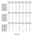
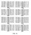
- the PLDs 50 and 52 that produce the X_INT_ADD bitsoperate as follows. First of all, referring to FIG. 8 , the disk drive address map is shown, in decimal and in hex. As seen, the disk drive addresses range from 0-14 in enclosure 0, up to 105-119 in enclosure 7. Now, referring to FIG. 9 , there is shown the manner in which the logic for the PLD 50 is derived. Shown in Chart 1 is the binary address for each of disk drives 0, 1, and 4-8 for each enclosure, labeled A-G from most significant to least significant bit. In other words, shown are the values that need to appear on the SEL_ID_X ⁇ 6:0> bits for each of these drives in each of the enclosures.
- the address of disk drive 0 in enclosure 0is 0, as can be seen in the first line.
- the address for disk drive 0 in enclosure 1is 15 decimal, or ‘F’ hex, as can be seen in line 2, and so on.
- certain patternstend to repeat for each column of bits (in other words, for multiple drives) as addresses between enclosures change.
- bit Gvaries in the same manner for disk drives 0, 4, 6, and 8.
- Bit Galso varies in the same manner for disk drives 1, 5, and 7, and in a manner inverse to that for the other drives.
- bit ‘F’varies in the same manner for disk drives 1, and 5.
- Bit ‘F’also varies in another manner for disk drives 0, 4, and 8.
- bit ‘F’ for disk 6varies in a manner inverse to that for disks 0, 4, and 8. Recognition of these patterns associated with each bit driven to each drive allows consolidation of addressing, such that X_INT_ADD bits are produced that will map to multiple SEL_ID_X bits.
- F1 and F2For bit F, there are two different repeating patterns, resulting in two equations, labeled F1 and F2.
- the pattern for disk drive 6is the negation of F1 and can be represented as !F1.
- the pattern for disk drive 7is the negation of F2 and can be represented as !F2.
- bit Ethere are four different repeating patterns. One pattern repeats for disk drives 0 and 8, and its negation occurs for disk drive 4. Another pattern occurs for disk drive 1, and its negation occurs for disk drive 5.
- Disk drives 6 and 7contain unique patterns and result in their own equations.
- bits A-G for each disk drive 0, 1, and 4-8can be represented by the equation that reflects the pattern for enclosures 0-7.
- the G bitis represented by equation G.
- the F bitis represented by equation F1.
- the E bitis represented by equation E1, and so on.
- the G bitis represented by the negation of equation G, shown as !G.
- the F bitis represented by equation F2.
- the E bitis represented by equation E2, and so on.
- Chart 3is completed in this manner for all disk drives 0, 1, and 4-8.
- the PLD 50is programmed to execute the equations of chart 2, and to produce the outputs required by the chart 3.
- A_INT_ADD_Xwherein X is one of the outputs designated in chart 3.
- the outputs of the PLD 50are A_INT_ADD_G, !A_INT_ADD_G, A_INT_ADD_F1, !A_INT_ADD_F1, A_INT_ADD_F2, !A_INT_ADD_F2, A_INT_ADD_E1, !A_INT_ADD_E1, A_INT_ADD_E2, A_INT_ADD_E3, A_INT_ADD_E4, A_INT_ADD_D1, !A_INT_ADD_D1, A_INT_ADD_D2, A_INT_ADD_D3, A_INT_ADD_D4, A_INT_ADD_D5, A_INT_ADD_D6, A_INT_ADD_C1, A_INT_ADD_C2, A_INT_ADD_C3, A_INT_ADD_C4, A_INT_ADD_C5, A_INT_ADD_C6, A_INT_ADD_B1, A_INT_ADD_
- the 49 SEL_ID_X ⁇ 6:0> bits that would be required for disk drives 0, 1, and 4-8are represented by 29 A_INT_ADD bits.
- the A_INT_ADD signalsare driven from the PLD 50 through series resistors 54 to drive the corresponding SEL_ID_X bits.
- A_INT_ADD_Gdrives SEL_ID 0 ⁇ 0>, SEL_ID — 4 ⁇ 0>, SEL_ID — 6 ⁇ 0>, and SEL_ID — 8 ⁇ 0>.
- A_INT_ADD_Gdrives SEL_ID — 1 ⁇ 0>, SEL_ID — 3 ⁇ 0>, SEL_ID — 5 ⁇ 0>, and SEL_ID — 7 ⁇ 0>.
- A_INT_ADD_F1drives SEL_ID0 ⁇ 1>, SEL_ID — 4 ⁇ 1>, and SEL_ID — 8 ⁇ 1>.
- !A_INT_ADD_F1drives SEL_ID — 6 ⁇ 1>.
- A_INT_ADD_F2drives SEL_ID — 1 ⁇ 1> and SEL_ID — 5 ⁇ 1>.
- !A_INT_ADD_F2drives SEL_ID — 7 ⁇ 1>.
- the remaining SEL_ID_X bitsare driven as shown in FIG. 11 , as determined by the chart 3.
- SEL_ID — 7 ⁇ 4> and SEL_ID — 8 ⁇ 4>could be driven by A_INT_ADD_G.
- the series resistors 54have been provided to isolate the various SEL_ID_X bits that are coupled to the same X_INT_ADD bit. For instance, SEL_ID — 0 ⁇ 0>, SEL_ID — 4 ⁇ 0>, SEL_ID — 6 ⁇ 0>, and SEL_ID — 8 ⁇ 0> are all driven by A_INT_ADD_G.
- the series resistorsisolate the A_INT_ADD_G bit from the fault so that the other functional SEL_ID_X bits can still be properly driven.
- a loading analysismight show that the fan-out for each X_INT_ADD bit should be limited so that its corresponding SEL_ID_X bits can in fact be driven in the event of a fault on one of them.
- duplicate X_INT_ADD bitscan be provided. This causes a small increase in the number of signals that must be routed across the midplane 30 .
- the A_INT_ADD_G and !A_INT_ADD_G bitshave been duplicated to reduce fan-out such that fan-out does not exceed 2.
- SEL_ID — 0 ⁇ 0> and SEL_ID — 4 ⁇ 0>are driven by A_INT_ADD_Ga
- SEL_ID — 6 ⁇ 0> and SEL_ID — 8 ⁇ 0>are driven by A_INT_ADD_Gb
- SEL_ID — 1 ⁇ 0> and SEL_ID — 5 ⁇ 0>are driven by !A_INT_ADD_Ga
- SEL_ID — 7 ⁇ 0>is driven by !A_INT_ADD_Gb. Note that, if fan-out requirement is changed such that fan-out should not exceed three, then !A_INT_ADD_Gb need not be provided, since !A_INT_ADD_G only drives three SEL_ID_X bits.
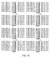
- the PLD 52produces B_INT_ADD ⁇ G:A> signals for disk drives 2, 3, and 9-14 in the same manner as was described for PLD 50 .
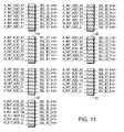
- the chart 4shows the various binary bit patterns for enclosures 0-7 for each of the disk drives 2, 3, and 9-14.
- the binary addressrange from decimal 2, hex 2, for enclosure 0 drive 2, up to decimal 119, hex 77, for enclosure 7 disk 14.
- the bit patterns for each bit A-Gare identified as previously described. The patterns are different for this set of drives. For example, Bit G consists of one pattern and its inverse, and is therefore represented by a single equation G.
- SEL_ID — 2 ⁇ 0>, SEL_ID — 10 ⁇ 0>, SEL_ID — 12 ⁇ 0>, and SEL_ID — 14 ⁇ 0>are driven by B_INT_ADD_G, while SEL_ID — 3 ⁇ 0>, SEL_ID — 3 ⁇ 0>, SEL_ID — 9 ⁇ 0>, SEL_ID — 11 ⁇ 0>, and SEL_ID — 13 ⁇ 0> are driven by !B_INT_ADD_G. All equations and charts (4-6) shown in FIG. 14 have been produced in exactly the same manner as was described with regard to FIG. 9 , based on the patterns existing in chart 6, and so do not require further description. As can be seen in FIG.
- the outputs B_INT_ADD_A2, B_INT_ADD_B1, B_INT_ADD_B2, B_INT_ADD_C2, B_INT_ADD_C3, B_INT_ADD_D1, !B_INT_ADD_D1, B_INT_ADD_D2, !B_INT_ADD_D2, B_INT_ADD_D3, B_INT_ADD_D4, B_INT_ADD_D5, B_INT_ADD_D6, B_INT_ADD_E1, !B_INT_ADD_E1, B_INT_ADD_E2, B_INT_ADD_E3, !B_INT_ADD_E3, B_INT_ADD_E4, B_INT_ADD_F1, !B_INT_ADD_F1, B_INT_ADD_F2, B_INT_ADD_F2, B_INT_ADD_G, !B_INT_ADD_Gare produced by the PLD 52 .
- the 56 SEL_ID_X bits that are needed to drive the disk drive 2, 3, and 9-14 address linescan be driven by only 25 signals, as seen in FIG. 16 . Again, the number of signals required can be further reduced where patterns overlap. For instance, the equations for B_INT_ADD_D2 and B_INT_ADD_E2 match, so one of these signals could be used to drive the corresponding SEL_ID_X bits. Also note that B_INT_ADD_C3 matches B_INT_ADD_G. So, as few as 23 signals can be used to drive the SEL_ID_X bits for drives 2, 3, and 9-14. And, as was previously described for PLD 50 , it may be desirable to limit the fan-out on the PLD 52 outputs.
- the ‘G’ bitis used to produce the B_INT_ADD_Ga and B_INT_ADD_Gb outputs.
- SEL_ID — 2 ⁇ 0> and SEL_ID — 10 ⁇ 0>are driven by B_INT_ADD_Ga.
- SEL_ID — 12 ⁇ 0> and SEL_ID — 14 ⁇ 0>are driven by B_INT_ADD_Gb.
- SEL_ID — 3 ⁇ 0> and SEL_ID — 9 ⁇ 0>are driven by !B_INT_ADD_Ga, while SEL_ID — 11 ⁇ 0> and SEL_ID — 13 ⁇ 0> are driven by !B_INT_ADD_Gb.
- a computing system or servermight have multiple copies of software in different areas of memory. Multiple power branches and addressing logic could be provided to access such memory in a highly available manner in accordance with the invention.
- the logichas been described in terms of certain types of logical functions, yet the skilled artisan will realize that there are many equivalent ways of implementing the described functionality, and that the described signals may be asserted at either a logical ‘1’ or ‘0’ level.
- the preferred embodimentemploys a Fibre Channel arbitrated loop architecture, the invention may be deployed with any channel or network protocol. All such modifications are intended to fall within the scope of the following appended claims. Accordingly, the claims set forth below should be construed in view of the full breadth and spirit of the present invention as disclosed herein.
Landscapes
- Engineering & Computer Science (AREA)
- Theoretical Computer Science (AREA)
- Quality & Reliability (AREA)
- Physics & Mathematics (AREA)
- General Engineering & Computer Science (AREA)
- General Physics & Mathematics (AREA)
- Signal Processing For Digital Recording And Reproducing (AREA)
Abstract
Description
Claims (24)
Priority Applications (1)
| Application Number | Priority Date | Filing Date | Title |
|---|---|---|---|
| US10/259,335US7254741B1 (en) | 2002-09-27 | 2002-09-27 | Attaining high availability through a power system branch architecture |
Applications Claiming Priority (1)
| Application Number | Priority Date | Filing Date | Title |
|---|---|---|---|
| US10/259,335US7254741B1 (en) | 2002-09-27 | 2002-09-27 | Attaining high availability through a power system branch architecture |
Publications (1)
| Publication Number | Publication Date |
|---|---|
| US7254741B1true US7254741B1 (en) | 2007-08-07 |
Family
ID=38324464
Family Applications (1)
| Application Number | Title | Priority Date | Filing Date |
|---|---|---|---|
| US10/259,335Expired - LifetimeUS7254741B1 (en) | 2002-09-27 | 2002-09-27 | Attaining high availability through a power system branch architecture |
Country Status (1)
| Country | Link |
|---|---|
| US (1) | US7254741B1 (en) |
Cited By (8)
| Publication number | Priority date | Publication date | Assignee | Title |
|---|---|---|---|---|
| US7445457B1 (en) | 2007-09-27 | 2008-11-04 | Emc Corporation | Techniques for connecting midplane connectors through a midplane |
| US20090216985A1 (en)* | 2008-02-22 | 2009-08-27 | International Business Machines Corporation | Methods, systems, and computer program products for dynamic selective memory mirroring |
| US20140204525A1 (en)* | 2013-01-23 | 2014-07-24 | Victor Key Pecone | Storage enclosure with independent storage device drawers |
| US20150100821A1 (en)* | 2013-10-09 | 2015-04-09 | Fujitsu Limited | Storage control apparatus, storage control system, and storage control method |
| US9098233B2 (en) | 2013-01-23 | 2015-08-04 | Dot Hill Systems Corporation | Storage device carrier for high density storage system |
| US9198322B2 (en) | 2013-01-23 | 2015-11-24 | Dot Hill Systems Corporation | Compliant drawer latch assembly |
| US9681576B2 (en) | 2013-01-23 | 2017-06-13 | Seagate Technology Llc | Shock dampening drawer slide |
| US9763350B2 (en) | 2013-01-23 | 2017-09-12 | Seagate Technology Llc | High density data storage system with improved storage device access |
Citations (15)
| Publication number | Priority date | Publication date | Assignee | Title |
|---|---|---|---|---|
| US4748560A (en) | 1984-10-15 | 1988-05-31 | Mitsubishi Denki Kabushiki Kaisha | Occupancy control system for plural serial buses |
| US5325363A (en)* | 1992-05-11 | 1994-06-28 | Tandem Computers Incorporated | Fault tolerant power supply for an array of storage devices |
| US5918241A (en)* | 1997-02-21 | 1999-06-29 | Lsi Logic Corporation | Method and apparatus for setting a plurality of addresses |
| US6351795B1 (en)* | 1997-09-05 | 2002-02-26 | Sun Microsystems, Inc. | Selective address translation in coherent memory replication |
| US6389554B1 (en)* | 1997-12-17 | 2002-05-14 | Electronics And Telecommunications Research Institute | Concurrent write duplex device |
| US6463504B1 (en)* | 1999-11-08 | 2002-10-08 | International Business Machines Corporation | Method and system for dynamically reassigning unused logical volumes from a storage subsystem to an open systems host |
| US6594745B2 (en)* | 2001-01-31 | 2003-07-15 | Hewlett-Packard Development Company, L.P. | Mirroring agent accessible to remote host computers, and accessing remote data-storage devices, via a communcations medium |
| US20030182501A1 (en)* | 2002-03-22 | 2003-09-25 | Elizabeth George | Method and system for dividing a plurality of existing volumes of storage into a plurality of virtual logical units of storage |
| US6651165B1 (en)* | 2000-11-13 | 2003-11-18 | Lsi Logic Corporation | Method and apparatus for directly booting a RAID volume as the primary operating system memory |
| US6687805B1 (en)* | 2000-10-30 | 2004-02-03 | Hewlett-Packard Development Company, L.P. | Method and system for logical-object-to-physical-location translation and physical separation of logical objects |
| US6725302B1 (en) | 1999-09-23 | 2004-04-20 | International Business Machines Corporation | Universal serial bus (USB) with wireless communication hubs |
| US6813686B1 (en)* | 2000-06-27 | 2004-11-02 | Emc Corporation | Method and apparatus for identifying logical volumes in multiple element computer storage domains |
| US6820139B1 (en)* | 2000-08-24 | 2004-11-16 | Lsi Logic Corporation | Method and architecture to associate enclosure service data with physical devices on a fibre channel loop with soft addresses |
| US6874100B2 (en)* | 2001-07-12 | 2005-03-29 | Digi-Data Corporation | Raid system with multiple controllers and proof against any single point of failure |
| US6889345B2 (en)* | 2001-10-19 | 2005-05-03 | Hewlett-Packard Development Company, Lp. | System and method for locating a failed storage device in a data storage system |
- 2002
- 2002-09-27USUS10/259,335patent/US7254741B1/ennot_activeExpired - Lifetime
Patent Citations (15)
| Publication number | Priority date | Publication date | Assignee | Title |
|---|---|---|---|---|
| US4748560A (en) | 1984-10-15 | 1988-05-31 | Mitsubishi Denki Kabushiki Kaisha | Occupancy control system for plural serial buses |
| US5325363A (en)* | 1992-05-11 | 1994-06-28 | Tandem Computers Incorporated | Fault tolerant power supply for an array of storage devices |
| US5918241A (en)* | 1997-02-21 | 1999-06-29 | Lsi Logic Corporation | Method and apparatus for setting a plurality of addresses |
| US6351795B1 (en)* | 1997-09-05 | 2002-02-26 | Sun Microsystems, Inc. | Selective address translation in coherent memory replication |
| US6389554B1 (en)* | 1997-12-17 | 2002-05-14 | Electronics And Telecommunications Research Institute | Concurrent write duplex device |
| US6725302B1 (en) | 1999-09-23 | 2004-04-20 | International Business Machines Corporation | Universal serial bus (USB) with wireless communication hubs |
| US6463504B1 (en)* | 1999-11-08 | 2002-10-08 | International Business Machines Corporation | Method and system for dynamically reassigning unused logical volumes from a storage subsystem to an open systems host |
| US6813686B1 (en)* | 2000-06-27 | 2004-11-02 | Emc Corporation | Method and apparatus for identifying logical volumes in multiple element computer storage domains |
| US6820139B1 (en)* | 2000-08-24 | 2004-11-16 | Lsi Logic Corporation | Method and architecture to associate enclosure service data with physical devices on a fibre channel loop with soft addresses |
| US6687805B1 (en)* | 2000-10-30 | 2004-02-03 | Hewlett-Packard Development Company, L.P. | Method and system for logical-object-to-physical-location translation and physical separation of logical objects |
| US6651165B1 (en)* | 2000-11-13 | 2003-11-18 | Lsi Logic Corporation | Method and apparatus for directly booting a RAID volume as the primary operating system memory |
| US6594745B2 (en)* | 2001-01-31 | 2003-07-15 | Hewlett-Packard Development Company, L.P. | Mirroring agent accessible to remote host computers, and accessing remote data-storage devices, via a communcations medium |
| US6874100B2 (en)* | 2001-07-12 | 2005-03-29 | Digi-Data Corporation | Raid system with multiple controllers and proof against any single point of failure |
| US6889345B2 (en)* | 2001-10-19 | 2005-05-03 | Hewlett-Packard Development Company, Lp. | System and method for locating a failed storage device in a data storage system |
| US20030182501A1 (en)* | 2002-03-22 | 2003-09-25 | Elizabeth George | Method and system for dividing a plurality of existing volumes of storage into a plurality of virtual logical units of storage |
Cited By (11)
| Publication number | Priority date | Publication date | Assignee | Title |
|---|---|---|---|---|
| US7445457B1 (en) | 2007-09-27 | 2008-11-04 | Emc Corporation | Techniques for connecting midplane connectors through a midplane |
| US20090216985A1 (en)* | 2008-02-22 | 2009-08-27 | International Business Machines Corporation | Methods, systems, and computer program products for dynamic selective memory mirroring |
| US8099570B2 (en)* | 2008-02-22 | 2012-01-17 | International Business Machines Corporation | Methods, systems, and computer program products for dynamic selective memory mirroring |
| US20140204525A1 (en)* | 2013-01-23 | 2014-07-24 | Victor Key Pecone | Storage enclosure with independent storage device drawers |
| US9098233B2 (en) | 2013-01-23 | 2015-08-04 | Dot Hill Systems Corporation | Storage device carrier for high density storage system |
| US9198322B2 (en) | 2013-01-23 | 2015-11-24 | Dot Hill Systems Corporation | Compliant drawer latch assembly |
| US9456515B2 (en)* | 2013-01-23 | 2016-09-27 | Seagate Technology Llc | Storage enclosure with independent storage device drawers |
| US9681576B2 (en) | 2013-01-23 | 2017-06-13 | Seagate Technology Llc | Shock dampening drawer slide |
| US9763350B2 (en) | 2013-01-23 | 2017-09-12 | Seagate Technology Llc | High density data storage system with improved storage device access |
| US20150100821A1 (en)* | 2013-10-09 | 2015-04-09 | Fujitsu Limited | Storage control apparatus, storage control system, and storage control method |
| US9542273B2 (en)* | 2013-10-09 | 2017-01-10 | Fujitsu Limited | Storage control apparatus, storage control system, and storage control method for failure detection and configuration of cascaded storage cabinets |
Similar Documents
| Publication | Publication Date | Title |
|---|---|---|
| EP0732653B1 (en) | Disk array system | |
| US6304942B1 (en) | Providing an upgrade path for an existing data storage system | |
| US5430855A (en) | Disk drive array memory system using nonuniform disk drives | |
| KR100270751B1 (en) | Method and system for automatic storage subsystem config uration | |
| US5146588A (en) | Redundancy accumulator for disk drive array memory | |
| US7099994B2 (en) | RAID memory system | |
| US6904556B2 (en) | Systems and methods which utilize parity sets | |
| US5835694A (en) | Raid-configured disk drive array wherein array control occurs at the disk drive level | |
| US7484050B2 (en) | High-density storage systems using hierarchical interconnect | |
| US20080276032A1 (en) | Arrangements which write same data as data stored in a first cache memory module, to a second cache memory module | |
| KR101506368B1 (en) | Active-active failover for a direct-attached storage system | |
| US8438429B2 (en) | Storage control apparatus and storage control method | |
| US20080059697A1 (en) | Storage system and control method for the same | |
| US20120017054A1 (en) | Storage sub-system and method for controlling the same | |
| US20040093472A1 (en) | Memory controllers with interleaved mirrored memory modes | |
| US20110029746A1 (en) | Reconfigurable memory module and method | |
| EP0535807A2 (en) | Linear and orthogonal expansion of array storage in multiprocessor computing systems | |
| US6961818B1 (en) | Method, system and computer program product for managing data in a mirrored cache using an access balancing technique | |
| CN100380351C (en) | Get data mask mapping information | |
| JPH05241870A (en) | Memory controller and its method | |
| US7254741B1 (en) | Attaining high availability through a power system branch architecture | |
| KR20010041461A (en) | Data storage system | |
| JP3554478B2 (en) | Memory array having redundant array and management method | |
| JP2008027312A (en) | Storage device and conversion board | |
| JPH05173722A (en) | Device for replacing multichannel data and parity |
Legal Events
| Date | Code | Title | Description |
|---|---|---|---|
| AS | Assignment | Owner name:EMC CORPORATION, MASSACHUSETTS Free format text:ASSIGNMENT OF ASSIGNORS INTEREST;ASSIGNORS:SARDELLA, STEVE D.;PEEKE, DOUGLAS E.;SYKES, TIMOTHY D.;REEL/FRAME:013347/0777 Effective date:20020926 | |
| STCF | Information on status: patent grant | Free format text:PATENTED CASE | |
| FEPP | Fee payment procedure | Free format text:PAYOR NUMBER ASSIGNED (ORIGINAL EVENT CODE: ASPN); ENTITY STATUS OF PATENT OWNER: LARGE ENTITY | |
| FPAY | Fee payment | Year of fee payment:4 | |
| FPAY | Fee payment | Year of fee payment:8 | |
| AS | Assignment | Owner name:THE BANK OF NEW YORK MELLON TRUST COMPANY, N.A., AS NOTES COLLATERAL AGENT, TEXAS Free format text:SECURITY AGREEMENT;ASSIGNORS:ASAP SOFTWARE EXPRESS, INC.;AVENTAIL LLC;CREDANT TECHNOLOGIES, INC.;AND OTHERS;REEL/FRAME:040136/0001 Effective date:20160907 Owner name:CREDIT SUISSE AG, CAYMAN ISLANDS BRANCH, AS COLLATERAL AGENT, NORTH CAROLINA Free format text:SECURITY AGREEMENT;ASSIGNORS:ASAP SOFTWARE EXPRESS, INC.;AVENTAIL LLC;CREDANT TECHNOLOGIES, INC.;AND OTHERS;REEL/FRAME:040134/0001 Effective date:20160907 Owner name:CREDIT SUISSE AG, CAYMAN ISLANDS BRANCH, AS COLLAT Free format text:SECURITY AGREEMENT;ASSIGNORS:ASAP SOFTWARE EXPRESS, INC.;AVENTAIL LLC;CREDANT TECHNOLOGIES, INC.;AND OTHERS;REEL/FRAME:040134/0001 Effective date:20160907 Owner name:THE BANK OF NEW YORK MELLON TRUST COMPANY, N.A., A Free format text:SECURITY AGREEMENT;ASSIGNORS:ASAP SOFTWARE EXPRESS, INC.;AVENTAIL LLC;CREDANT TECHNOLOGIES, INC.;AND OTHERS;REEL/FRAME:040136/0001 Effective date:20160907 | |
| AS | Assignment | Owner name:EMC IP HOLDING COMPANY LLC, MASSACHUSETTS Free format text:ASSIGNMENT OF ASSIGNORS INTEREST;ASSIGNOR:EMC CORPORATION;REEL/FRAME:040203/0001 Effective date:20160906 | |
| MAFP | Maintenance fee payment | Free format text:PAYMENT OF MAINTENANCE FEE, 12TH YEAR, LARGE ENTITY (ORIGINAL EVENT CODE: M1553); ENTITY STATUS OF PATENT OWNER: LARGE ENTITY Year of fee payment:12 | |
| AS | Assignment | Owner name:THE BANK OF NEW YORK MELLON TRUST COMPANY, N.A., T Free format text:SECURITY AGREEMENT;ASSIGNORS:CREDANT TECHNOLOGIES, INC.;DELL INTERNATIONAL L.L.C.;DELL MARKETING L.P.;AND OTHERS;REEL/FRAME:049452/0223 Effective date:20190320 Owner name:THE BANK OF NEW YORK MELLON TRUST COMPANY, N.A., TEXAS Free format text:SECURITY AGREEMENT;ASSIGNORS:CREDANT TECHNOLOGIES, INC.;DELL INTERNATIONAL L.L.C.;DELL MARKETING L.P.;AND OTHERS;REEL/FRAME:049452/0223 Effective date:20190320 | |
| AS | Assignment | Owner name:THE BANK OF NEW YORK MELLON TRUST COMPANY, N.A., TEXAS Free format text:SECURITY AGREEMENT;ASSIGNORS:CREDANT TECHNOLOGIES INC.;DELL INTERNATIONAL L.L.C.;DELL MARKETING L.P.;AND OTHERS;REEL/FRAME:053546/0001 Effective date:20200409 | |
| AS | Assignment | Owner name:WYSE TECHNOLOGY L.L.C., CALIFORNIA Free format text:RELEASE BY SECURED PARTY;ASSIGNOR:CREDIT SUISSE AG, CAYMAN ISLANDS BRANCH;REEL/FRAME:058216/0001 Effective date:20211101 Owner name:SCALEIO LLC, MASSACHUSETTS Free format text:RELEASE BY SECURED PARTY;ASSIGNOR:CREDIT SUISSE AG, CAYMAN ISLANDS BRANCH;REEL/FRAME:058216/0001 Effective date:20211101 Owner name:MOZY, INC., WASHINGTON Free format text:RELEASE BY SECURED PARTY;ASSIGNOR:CREDIT SUISSE AG, CAYMAN ISLANDS BRANCH;REEL/FRAME:058216/0001 Effective date:20211101 Owner name:MAGINATICS LLC, CALIFORNIA Free format text:RELEASE BY SECURED PARTY;ASSIGNOR:CREDIT SUISSE AG, CAYMAN ISLANDS BRANCH;REEL/FRAME:058216/0001 Effective date:20211101 Owner name:FORCE10 NETWORKS, INC., CALIFORNIA Free format text:RELEASE BY SECURED PARTY;ASSIGNOR:CREDIT SUISSE AG, CAYMAN ISLANDS BRANCH;REEL/FRAME:058216/0001 Effective date:20211101 Owner name:EMC IP HOLDING COMPANY LLC, TEXAS Free format text:RELEASE BY SECURED PARTY;ASSIGNOR:CREDIT SUISSE AG, CAYMAN ISLANDS BRANCH;REEL/FRAME:058216/0001 Effective date:20211101 Owner name:EMC CORPORATION, MASSACHUSETTS Free format text:RELEASE BY SECURED PARTY;ASSIGNOR:CREDIT SUISSE AG, CAYMAN ISLANDS BRANCH;REEL/FRAME:058216/0001 Effective date:20211101 Owner name:DELL SYSTEMS CORPORATION, TEXAS Free format text:RELEASE BY SECURED PARTY;ASSIGNOR:CREDIT SUISSE AG, CAYMAN ISLANDS BRANCH;REEL/FRAME:058216/0001 Effective date:20211101 Owner name:DELL SOFTWARE INC., CALIFORNIA Free format text:RELEASE BY SECURED PARTY;ASSIGNOR:CREDIT SUISSE AG, CAYMAN ISLANDS BRANCH;REEL/FRAME:058216/0001 Effective date:20211101 Owner name:DELL PRODUCTS L.P., TEXAS Free format text:RELEASE BY SECURED PARTY;ASSIGNOR:CREDIT SUISSE AG, CAYMAN ISLANDS BRANCH;REEL/FRAME:058216/0001 Effective date:20211101 Owner name:DELL MARKETING L.P., TEXAS Free format text:RELEASE BY SECURED PARTY;ASSIGNOR:CREDIT SUISSE AG, CAYMAN ISLANDS BRANCH;REEL/FRAME:058216/0001 Effective date:20211101 Owner name:DELL INTERNATIONAL, L.L.C., TEXAS Free format text:RELEASE BY SECURED PARTY;ASSIGNOR:CREDIT SUISSE AG, CAYMAN ISLANDS BRANCH;REEL/FRAME:058216/0001 Effective date:20211101 Owner name:DELL USA L.P., TEXAS Free format text:RELEASE BY SECURED PARTY;ASSIGNOR:CREDIT SUISSE AG, CAYMAN ISLANDS BRANCH;REEL/FRAME:058216/0001 Effective date:20211101 Owner name:CREDANT TECHNOLOGIES, INC., TEXAS Free format text:RELEASE BY SECURED PARTY;ASSIGNOR:CREDIT SUISSE AG, CAYMAN ISLANDS BRANCH;REEL/FRAME:058216/0001 Effective date:20211101 Owner name:AVENTAIL LLC, CALIFORNIA Free format text:RELEASE BY SECURED PARTY;ASSIGNOR:CREDIT SUISSE AG, CAYMAN ISLANDS BRANCH;REEL/FRAME:058216/0001 Effective date:20211101 Owner name:ASAP SOFTWARE EXPRESS, INC., ILLINOIS Free format text:RELEASE BY SECURED PARTY;ASSIGNOR:CREDIT SUISSE AG, CAYMAN ISLANDS BRANCH;REEL/FRAME:058216/0001 Effective date:20211101 | |
| AS | Assignment | Owner name:SCALEIO LLC, MASSACHUSETTS Free format text:RELEASE OF SECURITY INTEREST IN PATENTS PREVIOUSLY RECORDED AT REEL/FRAME (040136/0001);ASSIGNOR:THE BANK OF NEW YORK MELLON TRUST COMPANY, N.A., AS NOTES COLLATERAL AGENT;REEL/FRAME:061324/0001 Effective date:20220329 Owner name:EMC IP HOLDING COMPANY LLC (ON BEHALF OF ITSELF AND AS SUCCESSOR-IN-INTEREST TO MOZY, INC.), TEXAS Free format text:RELEASE OF SECURITY INTEREST IN PATENTS PREVIOUSLY RECORDED AT REEL/FRAME (040136/0001);ASSIGNOR:THE BANK OF NEW YORK MELLON TRUST COMPANY, N.A., AS NOTES COLLATERAL AGENT;REEL/FRAME:061324/0001 Effective date:20220329 Owner name:EMC CORPORATION (ON BEHALF OF ITSELF AND AS SUCCESSOR-IN-INTEREST TO MAGINATICS LLC), MASSACHUSETTS Free format text:RELEASE OF SECURITY INTEREST IN PATENTS PREVIOUSLY RECORDED AT REEL/FRAME (040136/0001);ASSIGNOR:THE BANK OF NEW YORK MELLON TRUST COMPANY, N.A., AS NOTES COLLATERAL AGENT;REEL/FRAME:061324/0001 Effective date:20220329 Owner name:DELL MARKETING CORPORATION (SUCCESSOR-IN-INTEREST TO FORCE10 NETWORKS, INC. AND WYSE TECHNOLOGY L.L.C.), TEXAS Free format text:RELEASE OF SECURITY INTEREST IN PATENTS PREVIOUSLY RECORDED AT REEL/FRAME (040136/0001);ASSIGNOR:THE BANK OF NEW YORK MELLON TRUST COMPANY, N.A., AS NOTES COLLATERAL AGENT;REEL/FRAME:061324/0001 Effective date:20220329 Owner name:DELL PRODUCTS L.P., TEXAS Free format text:RELEASE OF SECURITY INTEREST IN PATENTS PREVIOUSLY RECORDED AT REEL/FRAME (040136/0001);ASSIGNOR:THE BANK OF NEW YORK MELLON TRUST COMPANY, N.A., AS NOTES COLLATERAL AGENT;REEL/FRAME:061324/0001 Effective date:20220329 Owner name:DELL INTERNATIONAL L.L.C., TEXAS Free format text:RELEASE OF SECURITY INTEREST IN PATENTS PREVIOUSLY RECORDED AT REEL/FRAME (040136/0001);ASSIGNOR:THE BANK OF NEW YORK MELLON TRUST COMPANY, N.A., AS NOTES COLLATERAL AGENT;REEL/FRAME:061324/0001 Effective date:20220329 Owner name:DELL USA L.P., TEXAS Free format text:RELEASE OF SECURITY INTEREST IN PATENTS PREVIOUSLY RECORDED AT REEL/FRAME (040136/0001);ASSIGNOR:THE BANK OF NEW YORK MELLON TRUST COMPANY, N.A., AS NOTES COLLATERAL AGENT;REEL/FRAME:061324/0001 Effective date:20220329 Owner name:DELL MARKETING L.P. (ON BEHALF OF ITSELF AND AS SUCCESSOR-IN-INTEREST TO CREDANT TECHNOLOGIES, INC.), TEXAS Free format text:RELEASE OF SECURITY INTEREST IN PATENTS PREVIOUSLY RECORDED AT REEL/FRAME (040136/0001);ASSIGNOR:THE BANK OF NEW YORK MELLON TRUST COMPANY, N.A., AS NOTES COLLATERAL AGENT;REEL/FRAME:061324/0001 Effective date:20220329 Owner name:DELL MARKETING CORPORATION (SUCCESSOR-IN-INTEREST TO ASAP SOFTWARE EXPRESS, INC.), TEXAS Free format text:RELEASE OF SECURITY INTEREST IN PATENTS PREVIOUSLY RECORDED AT REEL/FRAME (040136/0001);ASSIGNOR:THE BANK OF NEW YORK MELLON TRUST COMPANY, N.A., AS NOTES COLLATERAL AGENT;REEL/FRAME:061324/0001 Effective date:20220329 | |
| AS | Assignment | Owner name:SCALEIO LLC, MASSACHUSETTS Free format text:RELEASE OF SECURITY INTEREST IN PATENTS PREVIOUSLY RECORDED AT REEL/FRAME (045455/0001);ASSIGNOR:THE BANK OF NEW YORK MELLON TRUST COMPANY, N.A., AS NOTES COLLATERAL AGENT;REEL/FRAME:061753/0001 Effective date:20220329 Owner name:EMC IP HOLDING COMPANY LLC (ON BEHALF OF ITSELF AND AS SUCCESSOR-IN-INTEREST TO MOZY, INC.), TEXAS Free format text:RELEASE OF SECURITY INTEREST IN PATENTS PREVIOUSLY RECORDED AT REEL/FRAME (045455/0001);ASSIGNOR:THE BANK OF NEW YORK MELLON TRUST COMPANY, N.A., AS NOTES COLLATERAL AGENT;REEL/FRAME:061753/0001 Effective date:20220329 Owner name:EMC CORPORATION (ON BEHALF OF ITSELF AND AS SUCCESSOR-IN-INTEREST TO MAGINATICS LLC), MASSACHUSETTS Free format text:RELEASE OF SECURITY INTEREST IN PATENTS PREVIOUSLY RECORDED AT REEL/FRAME (045455/0001);ASSIGNOR:THE BANK OF NEW YORK MELLON TRUST COMPANY, N.A., AS NOTES COLLATERAL AGENT;REEL/FRAME:061753/0001 Effective date:20220329 Owner name:DELL MARKETING CORPORATION (SUCCESSOR-IN-INTEREST TO FORCE10 NETWORKS, INC. AND WYSE TECHNOLOGY L.L.C.), TEXAS Free format text:RELEASE OF SECURITY INTEREST IN PATENTS PREVIOUSLY RECORDED AT REEL/FRAME (045455/0001);ASSIGNOR:THE BANK OF NEW YORK MELLON TRUST COMPANY, N.A., AS NOTES COLLATERAL AGENT;REEL/FRAME:061753/0001 Effective date:20220329 Owner name:DELL PRODUCTS L.P., TEXAS Free format text:RELEASE OF SECURITY INTEREST IN PATENTS PREVIOUSLY RECORDED AT REEL/FRAME (045455/0001);ASSIGNOR:THE BANK OF NEW YORK MELLON TRUST COMPANY, N.A., AS NOTES COLLATERAL AGENT;REEL/FRAME:061753/0001 Effective date:20220329 Owner name:DELL INTERNATIONAL L.L.C., TEXAS Free format text:RELEASE OF SECURITY INTEREST IN PATENTS PREVIOUSLY RECORDED AT REEL/FRAME (045455/0001);ASSIGNOR:THE BANK OF NEW YORK MELLON TRUST COMPANY, N.A., AS NOTES COLLATERAL AGENT;REEL/FRAME:061753/0001 Effective date:20220329 Owner name:DELL USA L.P., TEXAS Free format text:RELEASE OF SECURITY INTEREST IN PATENTS PREVIOUSLY RECORDED AT REEL/FRAME (045455/0001);ASSIGNOR:THE BANK OF NEW YORK MELLON TRUST COMPANY, N.A., AS NOTES COLLATERAL AGENT;REEL/FRAME:061753/0001 Effective date:20220329 Owner name:DELL MARKETING L.P. (ON BEHALF OF ITSELF AND AS SUCCESSOR-IN-INTEREST TO CREDANT TECHNOLOGIES, INC.), TEXAS Free format text:RELEASE OF SECURITY INTEREST IN PATENTS PREVIOUSLY RECORDED AT REEL/FRAME (045455/0001);ASSIGNOR:THE BANK OF NEW YORK MELLON TRUST COMPANY, N.A., AS NOTES COLLATERAL AGENT;REEL/FRAME:061753/0001 Effective date:20220329 Owner name:DELL MARKETING CORPORATION (SUCCESSOR-IN-INTEREST TO ASAP SOFTWARE EXPRESS, INC.), TEXAS Free format text:RELEASE OF SECURITY INTEREST IN PATENTS PREVIOUSLY RECORDED AT REEL/FRAME (045455/0001);ASSIGNOR:THE BANK OF NEW YORK MELLON TRUST COMPANY, N.A., AS NOTES COLLATERAL AGENT;REEL/FRAME:061753/0001 Effective date:20220329 | |
| AS | Assignment | Owner name:DELL MARKETING L.P. (ON BEHALF OF ITSELF AND AS SUCCESSOR-IN-INTEREST TO CREDANT TECHNOLOGIES, INC.), TEXAS Free format text:RELEASE OF SECURITY INTEREST IN PATENTS PREVIOUSLY RECORDED AT REEL/FRAME (053546/0001);ASSIGNOR:THE BANK OF NEW YORK MELLON TRUST COMPANY, N.A., AS NOTES COLLATERAL AGENT;REEL/FRAME:071642/0001 Effective date:20220329 Owner name:DELL INTERNATIONAL L.L.C., TEXAS Free format text:RELEASE OF SECURITY INTEREST IN PATENTS PREVIOUSLY RECORDED AT REEL/FRAME (053546/0001);ASSIGNOR:THE BANK OF NEW YORK MELLON TRUST COMPANY, N.A., AS NOTES COLLATERAL AGENT;REEL/FRAME:071642/0001 Effective date:20220329 Owner name:DELL PRODUCTS L.P., TEXAS Free format text:RELEASE OF SECURITY INTEREST IN PATENTS PREVIOUSLY RECORDED AT REEL/FRAME (053546/0001);ASSIGNOR:THE BANK OF NEW YORK MELLON TRUST COMPANY, N.A., AS NOTES COLLATERAL AGENT;REEL/FRAME:071642/0001 Effective date:20220329 Owner name:DELL USA L.P., TEXAS Free format text:RELEASE OF SECURITY INTEREST IN PATENTS PREVIOUSLY RECORDED AT REEL/FRAME (053546/0001);ASSIGNOR:THE BANK OF NEW YORK MELLON TRUST COMPANY, N.A., AS NOTES COLLATERAL AGENT;REEL/FRAME:071642/0001 Effective date:20220329 Owner name:EMC CORPORATION, MASSACHUSETTS Free format text:RELEASE OF SECURITY INTEREST IN PATENTS PREVIOUSLY RECORDED AT REEL/FRAME (053546/0001);ASSIGNOR:THE BANK OF NEW YORK MELLON TRUST COMPANY, N.A., AS NOTES COLLATERAL AGENT;REEL/FRAME:071642/0001 Effective date:20220329 Owner name:DELL MARKETING CORPORATION (SUCCESSOR-IN-INTEREST TO FORCE10 NETWORKS, INC. AND WYSE TECHNOLOGY L.L.C.), TEXAS Free format text:RELEASE OF SECURITY INTEREST IN PATENTS PREVIOUSLY RECORDED AT REEL/FRAME (053546/0001);ASSIGNOR:THE BANK OF NEW YORK MELLON TRUST COMPANY, N.A., AS NOTES COLLATERAL AGENT;REEL/FRAME:071642/0001 Effective date:20220329 Owner name:EMC IP HOLDING COMPANY LLC, TEXAS Free format text:RELEASE OF SECURITY INTEREST IN PATENTS PREVIOUSLY RECORDED AT REEL/FRAME (053546/0001);ASSIGNOR:THE BANK OF NEW YORK MELLON TRUST COMPANY, N.A., AS NOTES COLLATERAL AGENT;REEL/FRAME:071642/0001 Effective date:20220329 |