US7253497B2 - Integrated circuit with inductor having horizontal magnetic flux lines - Google Patents
Integrated circuit with inductor having horizontal magnetic flux linesDownload PDFInfo
- Publication number
- US7253497B2 US7253497B2US10/614,307US61430703AUS7253497B2US 7253497 B2US7253497 B2US 7253497B2US 61430703 AUS61430703 AUS 61430703AUS 7253497 B2US7253497 B2US 7253497B2
- Authority
- US
- United States
- Prior art keywords
- inductor
- integrated circuit
- conductor layers
- segment
- layers
- Prior art date
- Legal status (The legal status is an assumption and is not a legal conclusion. Google has not performed a legal analysis and makes no representation as to the accuracy of the status listed.)
- Expired - Lifetime
Links
- 230000004907fluxEffects0.000titleclaimsabstractdescription18
- 239000004020conductorSubstances0.000claimsabstractdescription40
- 239000010410layerSubstances0.000description68
- 239000000758substrateSubstances0.000description19
- 239000002184metalSubstances0.000description8
- 230000000694effectsEffects0.000description4
- 230000036962time dependentEffects0.000description4
- 239000003990capacitorSubstances0.000description3
- 238000000034methodMethods0.000description3
- 230000002411adverseEffects0.000description2
- 230000001419dependent effectEffects0.000description2
- 238000004519manufacturing processMethods0.000description2
- 230000008878couplingEffects0.000description1
- 238000010168coupling processMethods0.000description1
- 238000005859coupling reactionMethods0.000description1
- 230000007423decreaseEffects0.000description1
- 230000018109developmental processEffects0.000description1
- 238000010348incorporationMethods0.000description1
- 230000001939inductive effectEffects0.000description1
- 239000012212insulatorSubstances0.000description1
- 239000011229interlayerSubstances0.000description1
- 238000001465metallisationMethods0.000description1
- 229910021420polycrystalline siliconInorganic materials0.000description1
- 229920005591polysiliconPolymers0.000description1
- 230000011218segmentationEffects0.000description1
- 239000004065semiconductorSubstances0.000description1
- 239000002699waste materialSubstances0.000description1
Images


Classifications
- H—ELECTRICITY
- H10—SEMICONDUCTOR DEVICES; ELECTRIC SOLID-STATE DEVICES NOT OTHERWISE PROVIDED FOR
- H10D—INORGANIC ELECTRIC SEMICONDUCTOR DEVICES
- H10D1/00—Resistors, capacitors or inductors
- H10D1/20—Inductors
- H—ELECTRICITY
- H01—ELECTRIC ELEMENTS
- H01L—SEMICONDUCTOR DEVICES NOT COVERED BY CLASS H10
- H01L23/00—Details of semiconductor or other solid state devices
- H01L23/52—Arrangements for conducting electric current within the device in operation from one component to another, i.e. interconnections, e.g. wires, lead frames
- H01L23/522—Arrangements for conducting electric current within the device in operation from one component to another, i.e. interconnections, e.g. wires, lead frames including external interconnections consisting of a multilayer structure of conductive and insulating layers inseparably formed on the semiconductor body
- H01L23/5227—Inductive arrangements or effects of, or between, wiring layers
- H—ELECTRICITY
- H01—ELECTRIC ELEMENTS
- H01L—SEMICONDUCTOR DEVICES NOT COVERED BY CLASS H10
- H01L2924/00—Indexing scheme for arrangements or methods for connecting or disconnecting semiconductor or solid-state bodies as covered by H01L24/00
- H01L2924/0001—Technical content checked by a classifier
- H01L2924/0002—Not covered by any one of groups H01L24/00, H01L24/00 and H01L2224/00
Definitions
- This inventionrelates to semiconductor integrated circuits (ICs) having inductors formed therein.
- this inventionrelates to new and improved techniques for forming an inductor having horizontal, rather than vertical, magnetic flux lines within the IC.
- a significant trend throughout IC developmenthas been to reduce the size of the components within the IC's. As the size is reduced, the performance requirements and design margins of the components become more stringent.
- One aspect of IC's that affects the performance requirements and design marginsis the interference between two components within the IC due to magnetic field generation by one or both of the components during operation of the IC.
- an inductor formed on an IC chipcan generate a relatively strong time-dependent magnetic field, which can induce current in other parts, or circuitry, of the IC, thereby affecting the performance of the other parts of the IC.
- inductive coupling between the inductor and other parts of the IC, such as the substrate of the ICcan reduce the quality of the inductor, thereby affecting the performance of the inductor.
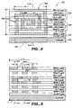
- FIGS. 1 and 2A typical on-chip inductor 100 formed on an IC 102 is shown in FIGS. 1 and 2 .
- the inductor 100is generally spiral-shaped, as seen in the top view in FIG. 2 . Additionally, the inductor 100 is typically located in one interconnect layer (a.k.a. “metal layers” and “conductor layers”) of the IC 102 , such as the top interconnect layer 104 .
- the inductor 100is, thus, generally formed by latitudinal and longitudinal conductors 106 within the top interconnect layer 104 .
- the IC 102also generally includes via layers and other interconnect layers 108 , a contact layer 110 and a substrate 112 ( FIG. 1 ).
- the substrate 112generally includes various structures and components, such as transistors, capacitors, etc. (not shown).
- the inductor 100is typically connected through the via layers and other interconnect layers 108 and the contact layer 110 to the substrate 112 by conductors 114 and 116 ( FIG. 1 ) that contact the inductor 100 at points 118 and 120 ( FIG. 2 ).
- a transverse magnetic fieldrepresented by magnetic flux lines 122 ( FIG. 1 ) is generated by the inductor 100 .
- the magnetic flux lines 122extend through the via layers and other interconnect layers 108 , the contact layer 110 and the substrate 112 .
- currentsare induced in the substrate 112 .
- the magnetic fieldis stronger nearer to the inductor 100 , as indicated by the density of the magnetic flux lines 122 , the magnetic field is still relatively strong down in the substrate 112 .
- the inductance of the inductor 100is relatively high, the effect of the magnetic field on the substrate 112 may be significant.
- the ground platetypically polysilicon or metal
- the guard ring 124is typically in the substrate 112 below the front end layers (not shown).
- the guard ring 124is typically a highly doped grounded region that is deeper than a well region. This option, however, takes up valuable space within the IC 102 and increases the cost of the IC 102 .
- Another optionis to locate the other components of the IC 102 in the substrate 112 at a sufficient distance from the inductor 100 that the magnetic field is too weak to have any significant effect on the performance of the other components. Thus, a region beneath the inductor 100 is free of any of the other components.
- This optionmay waste valuable space in the IC 102 and require conductor lines between components to be undesirably long to reach between opposite sides of the inductor 100 .
- the inductorsmay take up a significant percentage of the area of the IC, resulting in significantly fewer IC's per wafer if the other components cannot be placed close to the inductors.
- Another optionis to allow for sufficient margins in the design of the other components of the IC 102 . This option, however, results in a lower-performing IC.
- Another optionis to make the design of the inductor 100 more aggressive with lesser margins. This option, however, results in a more expensive IC.
- Another optionis to make the inductors larger to compensate for smaller quality factors. This option, however, may result in taking up a significant percentage of the IC's area with the inductors, increasing the size of the IC's and reducing the number of IC's per wafer.
- the present inventioninvolves an IC and a method of making an IC having at least one inductor that avoids the disadvantages described above.
- the geometry of the inductorminimizes the negative effects of the magnetic field thereof.
- a guard ringto attenuate the magnetic field of the inductor.
- other components of the ICcan be placed in close proximity to the inductor without having to alter the margins in the design of either the inductor or the other components to account for the magnetic field of the inductor.
- the inductoris essentially horizontal on the IC, so the magnetic flux lines are generally parallel to an over-all plane of the IC. In this manner, the region of highest magnetic flux density of the inductor is not near the substrate of the IC. In some embodiments, the region of highest magnetic flux density is preferably at the edge of the IC, away from the other components of the IC. Thus, at least one end of the inductor is preferably located near the edge of the IC.
- the inductorpreferably has a horizontal coil shape formed within multiple interconnect layers of the IC, instead of a spiral shape formed in just one interconnect layer, as described in the background. Additionally, the inductor has a generally rectangular cross-section. Each coil of the inductor, thus, has horizontal and vertical legs.
- the horizontal legsare preferably formed in conductor lines in the interconnect layers of the IC.
- the vertical legsare preferably formed in conductive vias in the dielectric layers, or “via layers,” between the interconnect layers as well as in the interconnect layers.
- the inductormay preferably include several inductor segments connected in series to form a single long inductor. Additionally, adjacent segments may preferably have their coil-shape in different spiraling angular directions, but their magnetic flux fields in the same orientation. Furthermore, some of the segments may preferably be spaced apart sufficiently to allow conductors between the segments to electrically connect other components of the IC.
- the segments of the inductormay preferably be connected with switches that can turn on and/or off the inductor segments, so the over-all inductance of the inductor can be changed.
- FIG. 1is a simplified, broken, cross-sectional view of portions of a prior art integrated circuit that includes a prior art inductor.
- FIG. 2is a simplified, broken, top view of the prior art integrated circuit, including the prior art inductor, shown in FIG. 1 .
- FIG. 3is a simplified schematic of portions of an integrated circuit, including an inductor, in which the present invention is incorporated and which has been fabricated according to the present invention.
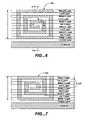
- FIGS. 4 , 5 and 6are simplified, broken, cross-sectional views of portions of the integrated circuit shown in FIG. 3 .
- FIGS. 7 , 8 and 9are simplified, broken, cross-sectional views of alternative embodiments of portions of the integrated circuit shown in FIG. 3 .
- FIG. 10is a simplified schematic of another alternative embodiment of portions of the integrated circuit shown in FIG. 3 .
- FIGS. 11 and 12are simplified schematics of additional alternative embodiments of portions of the integrated circuit shown in FIG. 3 .
- FIG. 3A portion of an integrated circuit (IC) 200 , such as a mixed analog IC, which incorporates the present invention and which is formed by the methodology of the present invention is shown in FIG. 3 .
- the IC 200includes an inductor 202 formed by a plurality of inductor segments 204 connected by electrical conductors 206 . Each segment 204 essentially forms one coil of the inductor 202 , so the inductor 202 is effectively a coil-shaped inductor.
- the IC 200also preferably includes a variety of other components 208 , such as transistors, capacitors, resistors, etc. located throughout the IC 200 , including adjacent (as shown) or under the inductor 202 .
- the inductor 202is formed as shown with one end 210 located near an edge 212 of the IC 200 and an opposite end 214 of the inductor 202 located near an opposite edge 216 of the IC 200 .
- a time-dependent magnetic field(indicated by magnetic flux lines 218 ) created by the inductor 202 upon operation of the IC 200 is generally parallel to an over-all x-y plane of the IC 200 .
- the region of greatest magnetic flux densityoccurs at the ends 210 and 214 of the inductor 202 near the edges 212 and 216 of the IC 200 .
- the other components 208 of the IC 200even if adjacent to (as shown) or under the inductor 202 , are not significantly affected by the magnetic field of the inductor 202 .
- the inductor 202is preferably formed as shown near another edge 220 of the IC 200 .
- the magnetic flux lines 218 along the length of the inductor 202extend off the edge 220 of the IC 200 , so there are no other components of the IC 200 in this area with which the inductor 202 could potentially inductively couple, even if the magnetic field was strong enough to do so in a significant manner.
- connection points 222 and 224are preferably at the ends 210 and 214 of the inductor 202 , or an inductor segment 204 , and can extend a distance beyond the inductor 202 before making contact to the other parts of the IC 200 .
- the IC 200further includes interconnect layers 226 (a.k.a. metal layers and conductor layers), ILD (interlayer dielectric) layers 228 (a.k.a. via layers and insulator layers), a contact layer 230 and a substrate (a.k.a. front-end layers) 232 , as shown in a cross-sectional view shown in FIG. 4 taken along section lines 4 - 4 in FIGS. 3 and 5 .
- the substrate 232generally includes various layers (not shown) that form the other components 208 ( FIG. 1 ), such as the transistors, capacitors, resistors, etc. of the IC 200 .
- the interconnect layers 226generally include conductors 234 (e.g. metal lines) that electrically connect various portions of the IC 200 .
- the ILD layers 228separate, or insulate, the interconnect layers 226 and generally include vias 236 (e.g. metal plugs) that electrically connect the conductors 234 between different interconnect layers 226 .
- the contact layer 230generally separates the substrate 232 from the first interconnect layer 226 .
- Combinations of the conductors 234 and the vias 236 within the interconnect layers 226 and the ILD layers 228 , respectively,enable electrical connections between the various components of the IC 200 .
- a ground planecan be used to isolate the inductor from the components in the IC 200 .
- the inductor segments 204are formed within the interconnect layers 226 and the ILD layers 228 .
- the inductor segments 204have a generally rectangular spiraling coil-shape, as shown in FIG. 4 .
- the rectangular spiraling coil-shapegenerally includes horizontal and vertical legs.
- the horizontal legsare formed by the conductors 234 in the interconnect layers 226 .
- the vertical legsare formed by the vias 236 in the ILD layers 228 and by the conductors 234 in the interconnect layers 226 .
- the substrate 232includes a region 238 that is directly beneath the inductor segments 204 and substantially free of the other components 208 ( FIG. 3 ). Since many of the other components 208 are electrically connected to the conductors in the interconnect layers 226 directly above the other components 208 , it may be impractical to place any of the other components 208 directly beneath the inductor 202 ( FIG. 3 ), because the inductor segments 204 take up all of the interconnect layers 226 within a width (w) of the inductor segments 204 .
- the inductor segments 204do not take up all of the interconnect layers 226 . Instead, at least one of the interconnect layers 226 , such as the first interconnect layer 226 (metal 1 layer), is unused by the inductor segments 204 . In this manner, the region 238 directly beneath the inductor segments 204 may include some of the other components 208 ( FIG. 3 ) electrically connected to at least one of the interconnect layers 226 , preferably between the inductor segments 204 and the region 238 . In a further embodiment, the inductor 202 ( FIG. 3 ) does not use any of the interconnect layers 226 used by the other components 208 ( FIG. 3 ) of the IC 200 ( FIG. 3 ).
- the inductor 202is formed in additional layers 226 and 228 formed above the interconnect layers 226 used by the other components 208 , so the region 238 below the inductor 202 may be fully used for the other components 208 .
- Use of either of these embodimentsmay depend on space requirements of the particular application for which the IC 200 is designed.
- the time-dependent magnetic field of the inductor 202does not significantly adversely affect the other components 208 in the region 238 , since the density of the magnetic field is relatively low along the length of the inductor 202 .
- a ground plate(not shown) can be used to isolate the inductor 202 from the other components 208 in the IC 200 .
- the inductor segments 204are connected to each other through the interconnect layers 226 , as shown in a cross-sectional view in FIG. 5 taken along section lines 5 - 5 in FIGS. 3 , 4 and 6 .
- the left inductor segment 204is connected to the middle inductor segment 204 by a conductor 240 only in the third interconnect layer 226 (metal 3 layer).
- the middle inductor segment 204is connected to the right inductor segment 204 by a conductor 242 only in the sixth interconnect layer 226 (metal 6 layer).
- the cross-sections of the inductor segments 204preferably alternate according to the examples shown in FIGS. 4 and 6 .
- the cross-section of the left inductor segment 204is illustrated by FIG. 4 , described above.
- the cross-section of the middle inductor segment 204is illustrated by the cross-sectional view shown in FIG. 6 , taken along section lines 6 - 6 in FIG. 5 .
- the cross-section of the right inductor segment 204is similar to FIG. 4 .
- the next inductor segment (not shown in FIG. 5 ) in the seriesreturns to FIG. 6 , and so on.
- the cross-sections shown in FIGS. 4 and 6are generally mirror images of each other, so the coil-shape of each inductor segment 204 is in an opposite spiraling angular direction from that of the inductor segments 204 on either side of it.
- each two inductor segments 204 in a roware connected through only one interconnect layer 226 , and the coil-shapes of each two inductor segments 204 in a row have opposite spiraling angular directions.
- the currentflows through the coil-shapes of each of the inductor segments 204 in the same angular direction (as exemplified by arrows A and B in FIGS. 4 and 6 , respectively).
- the magnetic field created by the current flowing through each of the inductor segments 204is oriented in the same direction (as exemplified by arrows C, D and E in FIG. 5 ).
- the over-all inductance of the inductor 202( FIG. 3 ) is generally dependent on the sum of the individual inductances of the inductor segments 204 , since the inductor segments 204 are connected in series. With more inductor segments 204 , the over-all inductance of the inductor 202 increases. A greater length (l) ( FIG. 5 ) of each inductor segment 204 , however, reduces the number of inductor segments 204 that can fit within the over-all length of the inductor 202 , and thereby reduces the over-all inductance of the inductor 202 . The greater length (l) also decreases the resistance of each conductor 234 and via 236 ( FIG. 4 ) that form the inductor segments 204 . Therefore, there is a tradeoff between higher inductance and lower resistance.
- each inductor segment 204generally depends on, among other factors, the width (w) and height (h) dimensions ( FIG. 4 ) of the cross-section of the inductor segment 204 and the number of turns of the coil-shape within these dimensions.
- the height (h) and number of turnsare generally dependent on the number of interconnect layers 226 ( FIGS. 4 , 5 and 6 ) used in the IC 200 .
- FIGS. 7 and 8show alternative embodiments with different numbers of interconnect layers 226 .
- FIG. 7shows only five interconnect layers 226 , thereby allowing for a lower height (h) and fewer turns.
- FIG. 7shows only five interconnect layers 226 , thereby allowing for a lower height (h) and fewer turns.
- FIG. 8shows seven interconnect layers 226 , thereby allowing for a greater height (h) and more turns. Design considerations for the height (h) and number of turns are, therefore, relatively constrained.
- the width (w), however,is not so constrained. Instead, the width (w) may be formed at almost any dimension to obtain the desired inductance for the inductor segments 204 and the over-all inductance of the inductor 202 ( FIG. 3 ).
- FIG. 9shows an inductor segment 204 having a shorter width (w) than the inductor segments 204 shown in FIGS. 4 and 6 . Larger widths (w) may be constrained only by the maximum required inductance of the inductor 202 and/or the size requirements for the IC 200 ( FIG. 3 ).
- more than one inductor 244 and 246is included in the IC 200 , as shown in FIG. 10 .
- the inductors 244 and 246may be electrically connected together, preferably in series, by a conductor 248 to combine their inductances.
- the inductors 244 and 246may also be offset from each other at any appropriate locations in the IC 200 and have any appropriate length, width and number of inductor segments 204 ( FIGS. 3-9 ).
- N inductors 250 , 252 , 254 and 256are connected together in series by conductors 258 and with switches 260 (e.g. transistors, fuse legs, etc.) by which the over-all inductance and/or quality factor value of the combined inductors 250 - 256 may be set or controlled, as shown in FIGS. 11 and 12 .
- the switches 260electrically connect the conductors 258 between each adjacent pair of the inductors 250 - 256 to chip circuitry 262 , which is similar to the substrate 232 ( FIGS. 4-9 ).
- the switches 260are each electrically connected to the conductors 258 in parallel with a corresponding one of the inductors 250 - 256 .
- the first and last inductors 250 and 256are connected to the chip circuitry 262 .
- the inductors 250 - 256 that correspond to any of the switches 260 that are “on”are effectively short-circuited out of contributing to the over-all inductance and/or quality factor of the combined inductors 250 - 256 .
- the over-all inductance of the combined inductors 250 - 256can be set by selecting which of the switches 260 are to be on and which are to be off.
- the present inventionenables the incorporation of one or more inductors into an IC with a relatively high level of flexibility in the design and relatively little adverse impact on other parts of the IC.
- the present inventionenables less expensive IC's due to the lower required design margins for components of the IC and higher performing IC's due to the higher quality factor of the inductor.
- the inductorsare formed by conventional conductors and vias in the interconnect layers and ILD layers, the fabrication of the inductors can be incorporated into existing metalization procedures without increasing the time or cost to fabricate the over-all IC.
- the time-dependent magnetic field of the inductoris relatively minor along the length of the inductor, other components of the IC can be placed in close proximity to the inductor and the inductor can be placed in almost any location in the IC, thereby more efficiently utilizing the available space in the IC.
- segmentation of the inductor or the use of more than one inductorallows for control of the over-all inductance during design or operation of the IC by turning on or off selected inductors or inductor segments.
Landscapes
- Physics & Mathematics (AREA)
- Condensed Matter Physics & Semiconductors (AREA)
- General Physics & Mathematics (AREA)
- Engineering & Computer Science (AREA)
- Computer Hardware Design (AREA)
- Microelectronics & Electronic Packaging (AREA)
- Power Engineering (AREA)
- Semiconductor Integrated Circuits (AREA)
- Coils Or Transformers For Communication (AREA)
Abstract
Description
Claims (5)
Priority Applications (2)
| Application Number | Priority Date | Filing Date | Title |
|---|---|---|---|
| US10/614,307US7253497B2 (en) | 2003-07-02 | 2003-07-02 | Integrated circuit with inductor having horizontal magnetic flux lines |
| US11/811,519US7384801B2 (en) | 2003-07-02 | 2007-06-11 | Integrated circuit with inductor having horizontal magnetic flux lines |
Applications Claiming Priority (1)
| Application Number | Priority Date | Filing Date | Title |
|---|---|---|---|
| US10/614,307US7253497B2 (en) | 2003-07-02 | 2003-07-02 | Integrated circuit with inductor having horizontal magnetic flux lines |
Related Child Applications (1)
| Application Number | Title | Priority Date | Filing Date |
|---|---|---|---|
| US11/811,519DivisionUS7384801B2 (en) | 2003-07-02 | 2007-06-11 | Integrated circuit with inductor having horizontal magnetic flux lines |
Publications (2)
| Publication Number | Publication Date |
|---|---|
| US20050003562A1 US20050003562A1 (en) | 2005-01-06 |
| US7253497B2true US7253497B2 (en) | 2007-08-07 |
Family
ID=33552819
Family Applications (2)
| Application Number | Title | Priority Date | Filing Date |
|---|---|---|---|
| US10/614,307Expired - LifetimeUS7253497B2 (en) | 2003-07-02 | 2003-07-02 | Integrated circuit with inductor having horizontal magnetic flux lines |
| US11/811,519Expired - LifetimeUS7384801B2 (en) | 2003-07-02 | 2007-06-11 | Integrated circuit with inductor having horizontal magnetic flux lines |
Family Applications After (1)
| Application Number | Title | Priority Date | Filing Date |
|---|---|---|---|
| US11/811,519Expired - LifetimeUS7384801B2 (en) | 2003-07-02 | 2007-06-11 | Integrated circuit with inductor having horizontal magnetic flux lines |
Country Status (1)
| Country | Link |
|---|---|
| US (2) | US7253497B2 (en) |
Cited By (4)
| Publication number | Priority date | Publication date | Assignee | Title |
|---|---|---|---|---|
| US20050003562A1 (en)* | 2003-07-02 | 2005-01-06 | Bhatt Hemanshu D. | Integrated circuit with inductor having horizontal magnetic flux lines |
| US20100289118A1 (en)* | 2009-05-12 | 2010-11-18 | Kabushiki Kaisha Toshiba | Semiconductor device |
| US8531250B1 (en)* | 2011-03-22 | 2013-09-10 | Netlogic Microsystems, Inc. | Configuring a tunable inductor across multiple layers of an integrated circuit |
| US9817036B2 (en) | 2012-11-06 | 2017-11-14 | Nxp Usa, Inc. | High bandwidth current sensor and method therefor |
Families Citing this family (20)
| Publication number | Priority date | Publication date | Assignee | Title |
|---|---|---|---|---|
| US7002228B2 (en) | 2003-02-18 | 2006-02-21 | Micron Technology, Inc. | Diffusion barrier for improving the thermal stability of MRAM devices |
| DE102005045059B4 (en)* | 2005-09-21 | 2011-05-19 | Infineon Technologies Ag | Integrated circuit arrangement with several Leitstrukturlagen and coil and method for manufacturing |
| US7679162B2 (en)* | 2005-12-19 | 2010-03-16 | Silicon Laboratories Inc. | Integrated current sensor package |
| US7990132B2 (en)* | 2006-06-30 | 2011-08-02 | Silicon Laboratories Inc. | Current sensor including an integrated circuit die including a first and second coil |
| US7999383B2 (en)* | 2006-07-21 | 2011-08-16 | Bae Systems Information And Electronic Systems Integration Inc. | High speed, high density, low power die interconnect system |
| US20080185679A1 (en)* | 2006-10-19 | 2008-08-07 | United Microelectronics Corp. | Inductor layout and manufacturing method thereof |
| US20080204183A1 (en)* | 2007-02-23 | 2008-08-28 | Infineon Technologies Ag | 3d-coil for saving area used by inductances |
| US7750408B2 (en) | 2007-03-29 | 2010-07-06 | International Business Machines Corporation | Integrated circuit structure incorporating an inductor, a conductive sheet and a protection circuit |
| US7728578B2 (en)* | 2008-05-15 | 2010-06-01 | Silicon Laboratories Inc. | Method and apparatus for high current measurement |
| US8393077B2 (en)* | 2009-09-15 | 2013-03-12 | Hewlett-Packard Development Company, L.P. | Fabrication of passive electronic components |
| JP5675504B2 (en)* | 2010-08-06 | 2015-02-25 | ルネサスエレクトロニクス株式会社 | Semiconductor device, electronic device, and manufacturing method of semiconductor device |
| US20120154102A1 (en)* | 2010-12-16 | 2012-06-21 | Shi-Bai Chen | Electrical fuse structure |
| US9559053B2 (en) | 2011-04-21 | 2017-01-31 | Taiwan Semiconductor Manufacturing Company, Ltd. | Compact vertical inductors extending in vertical planes |
| US8742539B2 (en)* | 2012-07-27 | 2014-06-03 | Infineon Technologies Austria Ag | Semiconductor component and method for producing a semiconductor component |
| US10008316B2 (en) | 2014-03-28 | 2018-06-26 | Qualcomm Incorporated | Inductor embedded in a package substrate |
| US12051534B2 (en) | 2021-04-09 | 2024-07-30 | Qualcomm Incorporated | Three dimensional (3D) vertical spiral inductor and transformer |
| US12131863B2 (en)* | 2021-04-20 | 2024-10-29 | Macronix International Co., Ltd. | Inductor structure and manufacturing method for the same |
| WO2023075846A1 (en)* | 2021-10-27 | 2023-05-04 | Microchip Technology Incorporated | Integrated inductor with inductor wire formed in an integrated circuit layer stack |
| US12272639B2 (en)* | 2021-10-27 | 2025-04-08 | Microchip Technology Incorporated | Integrated inductor with inductor wire formed in an integrated circuit layer stack |
| CN115188735A (en)* | 2022-07-11 | 2022-10-14 | 北京锐达芯集成电路设计有限责任公司 | A kind of semiconductor structure and its manufacturing method |
Citations (3)
| Publication number | Priority date | Publication date | Assignee | Title |
|---|---|---|---|---|
| US5793272A (en)* | 1996-08-23 | 1998-08-11 | International Business Machines Corporation | Integrated circuit toroidal inductor |
| US6291872B1 (en)* | 1999-11-04 | 2001-09-18 | Taiwan Semiconductor Manufacturing Co., Ltd. | Three-dimensional type inductor for mixed mode radio frequency device |
| US6925701B2 (en)* | 2003-03-13 | 2005-08-09 | Checkpoint Systems, Inc. | Method of making a series of resonant frequency tags |
Family Cites Families (1)
| Publication number | Priority date | Publication date | Assignee | Title |
|---|---|---|---|---|
| US7253497B2 (en)* | 2003-07-02 | 2007-08-07 | Lsi Corporation | Integrated circuit with inductor having horizontal magnetic flux lines |
- 2003
- 2003-07-02USUS10/614,307patent/US7253497B2/ennot_activeExpired - Lifetime
- 2007
- 2007-06-11USUS11/811,519patent/US7384801B2/ennot_activeExpired - Lifetime
Patent Citations (3)
| Publication number | Priority date | Publication date | Assignee | Title |
|---|---|---|---|---|
| US5793272A (en)* | 1996-08-23 | 1998-08-11 | International Business Machines Corporation | Integrated circuit toroidal inductor |
| US6291872B1 (en)* | 1999-11-04 | 2001-09-18 | Taiwan Semiconductor Manufacturing Co., Ltd. | Three-dimensional type inductor for mixed mode radio frequency device |
| US6925701B2 (en)* | 2003-03-13 | 2005-08-09 | Checkpoint Systems, Inc. | Method of making a series of resonant frequency tags |
Non-Patent Citations (2)
| Title |
|---|
| Marc T. Thompson, Inductance Calculation Techniques-Part II: Approximations and Handbook Methods, "Power Control and Intelligent Motion," Dec. 1999, website http://www.pcim.com, http://members.aol.com/Marcttpapers2/Induct2.pdf. |
| Steve Moshier, Calculation of electrical inductance-COIL02 Electrical Inductance Calculator, Jan. 2002, http://www.moshier.net/coildoc.html. |
Cited By (6)
| Publication number | Priority date | Publication date | Assignee | Title |
|---|---|---|---|---|
| US20050003562A1 (en)* | 2003-07-02 | 2005-01-06 | Bhatt Hemanshu D. | Integrated circuit with inductor having horizontal magnetic flux lines |
| US20070254448A1 (en)* | 2003-07-02 | 2007-11-01 | Lsi Logic Corporation | Integrated circuit with inductor having horizontal magnetic flux lines |
| US7384801B2 (en)* | 2003-07-02 | 2008-06-10 | Lsi Corporation | Integrated circuit with inductor having horizontal magnetic flux lines |
| US20100289118A1 (en)* | 2009-05-12 | 2010-11-18 | Kabushiki Kaisha Toshiba | Semiconductor device |
| US8531250B1 (en)* | 2011-03-22 | 2013-09-10 | Netlogic Microsystems, Inc. | Configuring a tunable inductor across multiple layers of an integrated circuit |
| US9817036B2 (en) | 2012-11-06 | 2017-11-14 | Nxp Usa, Inc. | High bandwidth current sensor and method therefor |
Also Published As
| Publication number | Publication date |
|---|---|
| US20070254448A1 (en) | 2007-11-01 |
| US7384801B2 (en) | 2008-06-10 |
| US20050003562A1 (en) | 2005-01-06 |
Similar Documents
| Publication | Publication Date | Title |
|---|---|---|
| US7384801B2 (en) | Integrated circuit with inductor having horizontal magnetic flux lines | |
| US8653926B2 (en) | Inductive and capacitive elements for semiconductor technologies with minimum pattern density requirements | |
| CN100468717C (en) | Planar inductive component and integrated circuit comprising a planar inductive component | |
| US6593838B2 (en) | Planar inductor with segmented conductive plane | |
| US7808358B2 (en) | Inductor and method for fabricating the same | |
| TWI395240B (en) | Integrated semiconductor inductor and its forming method and integrated semiconductor filter | |
| US6387747B1 (en) | Method to fabricate RF inductors with minimum area | |
| US8427266B2 (en) | Integrated circuit inductor having a patterned ground shield | |
| CN101266964B (en) | Semiconductor device with high-frequency interconnection | |
| US20070267718A1 (en) | Multilayer winding inductor | |
| US7064411B2 (en) | Spiral inductor and transformer | |
| US8003529B2 (en) | Method of fabrication an integrated circuit | |
| US7724116B2 (en) | Symmetrical inductor | |
| US7391292B2 (en) | Inductors having interconnect and inductor portions to provide combined magnetic fields | |
| US7312683B1 (en) | Symmetrical inductor | |
| US20150340423A1 (en) | Semiconductor device having inductor | |
| JP2006066769A (en) | Inductor and manufacturing method thereof | |
| TW200917289A (en) | Spiral inductor device | |
| JP2008047718A (en) | Semiconductor device | |
| US10103217B2 (en) | Semiconductor device having inductor | |
| US7477125B1 (en) | Symmetrical inductor device | |
| US12073973B1 (en) | Opposite-facing interleaved transformer design | |
| CN117038293A (en) | Active under-shield for coils and transformers |
Legal Events
| Date | Code | Title | Description |
|---|---|---|---|
| AS | Assignment | Owner name:LSI LOGIC CORPORATION, CALIFORNIA Free format text:ASSIGNMENT OF ASSIGNORS INTEREST;ASSIGNORS:BHATT, HEMANSHU D.;FURE, JAN;ALLMAN, DERRYL D.J.;REEL/FRAME:014296/0837 Effective date:20030624 | |
| STCF | Information on status: patent grant | Free format text:PATENTED CASE | |
| FEPP | Fee payment procedure | Free format text:PAYOR NUMBER ASSIGNED (ORIGINAL EVENT CODE: ASPN); ENTITY STATUS OF PATENT OWNER: LARGE ENTITY | |
| FPAY | Fee payment | Year of fee payment:4 | |
| AS | Assignment | Owner name:DEUTSCHE BANK AG NEW YORK BRANCH, AS COLLATERAL AG Free format text:PATENT SECURITY AGREEMENT;ASSIGNORS:LSI CORPORATION;AGERE SYSTEMS LLC;REEL/FRAME:032856/0031 Effective date:20140506 | |
| AS | Assignment | Owner name:LSI CORPORATION, CALIFORNIA Free format text:CHANGE OF NAME;ASSIGNOR:LSI LOGIC CORPORATION;REEL/FRAME:033102/0270 Effective date:20070406 | |
| FPAY | Fee payment | Year of fee payment:8 | |
| AS | Assignment | Owner name:AVAGO TECHNOLOGIES GENERAL IP (SINGAPORE) PTE. LTD Free format text:ASSIGNMENT OF ASSIGNORS INTEREST;ASSIGNOR:LSI CORPORATION;REEL/FRAME:035390/0388 Effective date:20140814 | |
| AS | Assignment | Owner name:LSI CORPORATION, CALIFORNIA Free format text:TERMINATION AND RELEASE OF SECURITY INTEREST IN PATENT RIGHTS (RELEASES RF 032856-0031);ASSIGNOR:DEUTSCHE BANK AG NEW YORK BRANCH, AS COLLATERAL AGENT;REEL/FRAME:037684/0039 Effective date:20160201 Owner name:AGERE SYSTEMS LLC, PENNSYLVANIA Free format text:TERMINATION AND RELEASE OF SECURITY INTEREST IN PATENT RIGHTS (RELEASES RF 032856-0031);ASSIGNOR:DEUTSCHE BANK AG NEW YORK BRANCH, AS COLLATERAL AGENT;REEL/FRAME:037684/0039 Effective date:20160201 | |
| AS | Assignment | Owner name:BANK OF AMERICA, N.A., AS COLLATERAL AGENT, NORTH CAROLINA Free format text:PATENT SECURITY AGREEMENT;ASSIGNOR:AVAGO TECHNOLOGIES GENERAL IP (SINGAPORE) PTE. LTD.;REEL/FRAME:037808/0001 Effective date:20160201 Owner name:BANK OF AMERICA, N.A., AS COLLATERAL AGENT, NORTH Free format text:PATENT SECURITY AGREEMENT;ASSIGNOR:AVAGO TECHNOLOGIES GENERAL IP (SINGAPORE) PTE. LTD.;REEL/FRAME:037808/0001 Effective date:20160201 | |
| AS | Assignment | Owner name:AVAGO TECHNOLOGIES GENERAL IP (SINGAPORE) PTE. LTD., SINGAPORE Free format text:TERMINATION AND RELEASE OF SECURITY INTEREST IN PATENTS;ASSIGNOR:BANK OF AMERICA, N.A., AS COLLATERAL AGENT;REEL/FRAME:041710/0001 Effective date:20170119 Owner name:AVAGO TECHNOLOGIES GENERAL IP (SINGAPORE) PTE. LTD Free format text:TERMINATION AND RELEASE OF SECURITY INTEREST IN PATENTS;ASSIGNOR:BANK OF AMERICA, N.A., AS COLLATERAL AGENT;REEL/FRAME:041710/0001 Effective date:20170119 | |
| AS | Assignment | Owner name:BELL SEMICONDUCTOR, LLC, ILLINOIS Free format text:ASSIGNMENT OF ASSIGNORS INTEREST;ASSIGNORS:AVAGO TECHNOLOGIES GENERAL IP (SINGAPORE) PTE. LTD.;BROADCOM CORPORATION;REEL/FRAME:044886/0001 Effective date:20171208 | |
| AS | Assignment | Owner name:CORTLAND CAPITAL MARKET SERVICES LLC, AS COLLATERA Free format text:SECURITY INTEREST;ASSIGNORS:HILCO PATENT ACQUISITION 56, LLC;BELL SEMICONDUCTOR, LLC;BELL NORTHERN RESEARCH, LLC;REEL/FRAME:045216/0020 Effective date:20180124 | |
| MAFP | Maintenance fee payment | Free format text:PAYMENT OF MAINTENANCE FEE, 12TH YEAR, LARGE ENTITY (ORIGINAL EVENT CODE: M1553); ENTITY STATUS OF PATENT OWNER: LARGE ENTITY Year of fee payment:12 | |
| AS | Assignment | Owner name:BELL NORTHERN RESEARCH, LLC, ILLINOIS Free format text:SECURITY INTEREST;ASSIGNOR:CORTLAND CAPITAL MARKET SERVICES LLC;REEL/FRAME:060885/0001 Effective date:20220401 Owner name:BELL SEMICONDUCTOR, LLC, ILLINOIS Free format text:SECURITY INTEREST;ASSIGNOR:CORTLAND CAPITAL MARKET SERVICES LLC;REEL/FRAME:060885/0001 Effective date:20220401 Owner name:HILCO PATENT ACQUISITION 56, LLC, ILLINOIS Free format text:SECURITY INTEREST;ASSIGNOR:CORTLAND CAPITAL MARKET SERVICES LLC;REEL/FRAME:060885/0001 Effective date:20220401 |