US7253426B2 - Structures and methods for coupling energy from an electromagnetic wave - Google Patents
Structures and methods for coupling energy from an electromagnetic waveDownload PDFInfo
- Publication number
- US7253426B2 US7253426B2US11/243,476US24347605AUS7253426B2US 7253426 B2US7253426 B2US 7253426B2US 24347605 AUS24347605 AUS 24347605AUS 7253426 B2US7253426 B2US 7253426B2
- Authority
- US
- United States
- Prior art keywords
- particle beam
- path
- charged particle
- varying field
- resonant structure
- Prior art date
- Legal status (The legal status is an assumption and is not a legal conclusion. Google has not performed a legal analysis and makes no representation as to the accuracy of the status listed.)
- Expired - Fee Related, expires
Links
Images


Classifications
- H—ELECTRICITY
- H01—ELECTRIC ELEMENTS
- H01J—ELECTRIC DISCHARGE TUBES OR DISCHARGE LAMPS
- H01J25/00—Transit-time tubes, e.g. klystrons, travelling-wave tubes, magnetrons
Definitions
- This disclosurerelates to coupling energy from an electromagnetic wave.
- Electromagnetic radiationis produced by the motion of electrically charged particles. Oscillating electrons produce electromagnetic radiation commensurate in frequency with the frequency of the oscillations. Electromagnetic radiation is essentially energy transmitted through space or through a material medium in the form of electromagnetic waves. The term can also refer to the emission and propagation of such energy. Whenever an electric charge oscillates or is accelerated, a disturbance characterized by the existence of electric and magnetic fields propagates outward from it. This disturbance is called an electromagnetic wave. Electromagnetic radiation falls into categories of wave types depending upon their frequency, and the frequency range of such waves is tremendous, as is shown by the electromagnetic spectrum in the following chart (which categorizes waves into types depending upon their frequency):
- the ability to generate (or detect) electromagnetic radiation of a particular typedepends upon the ability to create a structure suitable for electron oscillation or excitation at the frequency desired.
- Electromagnetic radiation at radio frequenciesfor example, is relatively easy to generate using relatively large or even somewhat small structures.
- Resonant structureshave been the basis for much of the presently known high frequency electronics. Devices like klystrons and magnetrons had electronics that moved frequencies of emission up to the megahertz range by the 1930s and 1940s. By around 1960, people were trying to reduce the size of resonant structures to get even higher frequencies, but had limited success because the Q of the devices went down due to the resistivity of the walls of the resonant structures. At about the same time, Smith and Purcell saw the first signs that free electrons could cause the emission of electromagnetic radiation in the visible range by running an electron beam past a diffraction grating. Since then, there has been much speculation as to what the physical basis for the Smith-Purcell radiation really is.
- Klystronsare now well-known structures for oscillating electrons and creating electromagnetic radiation in the microwave frequency.
- the structure and operation of klystronshas been well-studied and documented and will be readily understood by the artisan. However, for the purpose of background, the operation of the klystron will be described at a high level, leaving the particularities of such devices to the artisan's present understanding.
- Klystronsare a type of linear beam microwave tube.
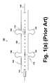
- a basic structure of a klystronis shown by way of example in FIG. 1( a ).
- a klystron structurewas described that involved a direct current stream of electrons within a vacuum cavity passing through an oscillating electric field.
- a klystron 100is shown as a high-vacuum device with a cathode 102 that emits a well-focused electron beam 104 past a number of cavities 106 that the beam traverses as it travels down a linear tube 108 to anode 103 .
- the cavitiesare sized and designed to resonate at or near the operating frequency of the tube.
- the principlein essence, involves conversion of the kinetic energy in the beam, imparted by a high accelerating voltage, to microwave energy. That conversion takes place as a result of the amplified RF (radio frequency) input signal causing the electrons in the beam to “bunch up” into so-called “bunches” (denoted 110 ) along the beam path as they pass the various cavities 106 . These bunches then give up their energy to the high-level induced RF fields at the output cavity.
- RFradio frequency
- the electron bunchesare formed when an oscillating electric field causes the electron stream to be velocity modulated so that some number of electrons increase in speed within the stream and some number of electrons decrease in speed within the stream.
- the bunches that are formedcreate a space-charge wave or charge-modulated electron beam.
- the bunchesAs the electron bunches pass the mouth of the output cavity, the bunches induce a large current, much larger than the input current. The induced current can then generate electromagnetic radiation.
- Traveling wave tubes(TWT)—first described in 1942—are another well-known type of linear microwave tube.
- a TWTincludes a source of electrons that travels the length of a microwave electronic tube, an attenuator, a helix delay line, radio frequency (RF) input and output, and an electron collector.
- RFradio frequency
- an electrical currentwas sent along the helical delay line to interact with the electron stream.
- Backwards wave devicesare also known and differ from TWTs in that they use a wave in which the power flow is opposite in direction from that of the electron beam.
- a backwards wave deviceuses the concept of a backward group velocity with a forward phase velocity. In this case, the RF power comes out at the cathode end of the device.
- Backward wave devicescould be amplifiers or oscillators.
- Magnetronsare another type of well-known resonance cavity structure developed in the 1920s to produce microwave radiation. While their external configurations can differ, each magnetron includes an anode, a cathode, a particular wave tube and a strong magnet.
- FIG. 1( b )shows an exemplary magnetron 112 .
- the anodeis shown as the (typically iron) external structure of the circular wave tube 114 and is interrupted by a number of cavities 116 interspersed around the tube 114 .
- the cathode 118is in the center of the magnetron, as shown. Absent a magnetic field, the cathode would send electrons directly outward toward the anode portions forming the tube 114 .
- reflex klystrona single cavity, through which the electron beam is passed, can produce the required microwave frequency oscillations.
- An example reflex klystron 120is shown in FIG. 1( c ).
- the cathode 122emits electrons toward the reflector plate 124 via an accelerator grid 126 and grids 128 .
- the reflex klystron 120has a single cavity 130 .
- the electron beamis modulated (as in other klystrons) by passing by the cavity 130 on its way away from the cathode 122 to the plate 124 .
- the electron beamis not terminated at an output cavity, but instead is reflected by the reflector plate 124 . The reflection provides the feedback necessary to maintain electron oscillations within the tube.
- the characteristic frequency of electron oscillationdepends upon the size, structure, and tuning of the resonant cavities.
- structureshave been discovered that create relatively low frequency radiation (radio and microwave levels), up to, for example, GHz levels, using these resonant structures. Higher levels of radiation are generally thought to be prohibitive because resistance in the cavity walls will dominate with smaller sizes and will not allow oscillation.
- aluminum and other metalscannot be machined down to sufficiently small sizes to form the cavities desired.
- visible light radiation in the range of 400 Terahertz–750 Terahertzis not known to be created by klystron-type structures.
- U.S. Pat. No. 6,373,194 to Smallillustrates the difficulty in obtaining small, high-frequency radiation sources.
- Smallsuggests a method of fabricating a micro-magnetron.
- the bunched electron beampasses the opening of the resonance cavity.
- the bunches of electronsmust pass the opening of the resonance cavity in less time than the desired output frequency.
- the electronsmust travel at very high speed and still remain confined.
- Surface plasmonscan be excited at a metal dielectric interface by a monochromatic light beam. The energy of the light is bound to the surface and propagates as an electromagnetic wave. Surface plasmons can propagate on the surface of a metal as well as on the interface between a metal and dielectric material. Bulk plasmons can propagate beneath the surface, although they are typically not energetically favored.
- Free electron lasersoffer intense beams of any wavelength because the electrons are free of any atomic structure.
- U.S. Pat. No. 4,740,973Madey et al. disclose a free electron laser.
- the free electron laserincludes a charged particle accelerator, a cavity with a straight section and an undulator.
- the acceleratorinjects a relativistic electron or positron beam into said straight section past an undulator mounted coaxially along said straight section.
- the undulatorperiodically modulates in space the acceleration of the electrons passing through it inducing the electrons to produce a light beam that is practically collinear with the axis of undulator.
- An optical cavityis defined by two mirrors mounted facing each other on either side of the undulator to permit the circulation of light thus emitted.
- Laser amplificationoccurs when the period of said circulation of light coincides with the period of passage of the electron packets and the optical gain per passage exceeds the light losses that occur in the optical cavity.
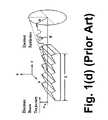
- Smith-Purcell radiationoccurs when a charged particle passes close to a periodically varying metallic surface, as depicted in FIG. 1( d ).
- Smith-Purcell devicesproduce visible light by passing an electron beam close to the surface of a diffraction grating.
- electronsare deflected by image charges in the grating at a frequency in the visible spectrum.
- the effectmay be a single electron event, but some devices can exhibit a change in slope of the output intensity versus current.
- Smith-Purcell devicesonly the energy of the electron beam and the period of the grating affect the frequency of the visible light emission.
- the beam currentis generally, but not always, small.
- Vermont Photonicsnotice an increase in output with their devices above a certain current density limit. Because of the nature of diffraction physics, the period of the grating must exceed the wavelength of light.
- Koops, et al., U.S. Pat. No. 6,909,104, published Nov. 30, 2000, ( ⁇ 102(e) date May 24, 2002)describe a miniaturized coherent terahertz free electron laser using a periodic grating for the undulator (sometimes referred to as the wiggler).
- Koops et al.describe a free electron laser using a periodic structure grating for the undulator (also referred to as the wiggler).
- Koopsproposes using standard electronics to bunch the electrons before they enter the undulator. The apparent object of this is to create coherent terahertz radiation. In one instance, Koops, et al.
- the diffraction gratinghas a length of approximately 1 mm to 1 cm, with grating periods of 0.5 to 10 microns, “depending on the wavelength of the terahertz radiation to be emitted.”
- Koopsproposes using standard electronics to bunch the electrons before they enter the undulator.
- Potylitsin“Resonant Diffraction Radiation and Smith-Purcell Effect,” 13 Apr. 1998, described an emission of electrons moving close to a periodic structure treated as the resonant diffraction radiation. Potylitsin's grating had “perfectly conducting strips spaced by a vacuum gap.”
- Smith-Purcell devicesare inefficient. Their production of light is weak compared to their input power, and they cannot be optimized. Current Smith-Purcell devices are not suitable for true visible light applications due at least in part to their inefficiency and inability to effectively produce sufficient photon density to be detectable without specialized equipment.
- Smith-Purcell devicesyielded poor light production efficiency. Rather than deflect the passing electron beam as Smith-Purcell devices do, we created devices that resonated at the frequency of light as the electron beam passes by. In this way, the device resonance matches the system resonance with resulting higher output. Our discovery has proven to produce visible light (or even higher or lower frequency radiation) at higher yields from optimized ultra-small physical structures.
- Coupling energy from electromagnetic waves in the terahertz range from 0.1 THz (about 3000 microns) to 700 THz (about 0.4 microns)is finding use in numerous new applications. These applications include improved detection of concealed weapons and explosives, improved medical imaging, finding biological materials, better characterization of semiconductors; and broadening the available bandwidth for wireless communications.
- the interaction between an electromagnetic wave and a charged particle, namely an electroncan occur via three basic processes: absorption, spontaneous emission and stimulated emission.
- the interactioncan provide a transfer of energy between the electromagnetic wave and the electron.
- photoconductor semiconductor devicesuse the absorption process to receive the electromagnetic wave and transfer energy to electron-hole pairs by band-to-band transitions.
- Electromagnetic waves having an energy level greater than a material's characteristic binding energycan create electrons that move when connected across a voltage source to provide a current.
- extrinsic photoconductor devicesoperate having transitions across forbidden-gap energy levels use the absorption process (S. M., Sze, “Semiconductor Devices Physics and Technology,” 2002).
- a measure of the energy coupled from an electromagnetic wave for the materialis referred to as an absorption coefficient.
- a point where the absorption coefficient decreases rapidlyis called a cutoff wavelength.
- the absorption coefficientis dependant on the particular material used to make a device.
- gallium arsenide (GaAs)absorbs electromagnetic wave energy from about 0.6 microns and has a cutoff wavelength of about 0.87 microns.
- silicon (Si)can absorb energy from about 0.4 microns and has a cutoff wavelength of about 1.1 microns.
- the ability to transfer energy to the electrons within the material for making the deviceis a function of the wavelength or frequency of the electromagnetic wave.
- CCDCharge Coupled Device
- Raman spectroscopyis a well-known means to measure the characteristics of molecule vibrations using laser radiation as the excitation source.
- a molecule to be analyzedis illuminated with laser radiation and the resulting scattered frequencies are collected in a detector and analyzed.
- the electromagnetic contributionoccurs when the laser radiation excites plasmon resonances in the metallic surface structures. These plasmons induce local fields of electromagnetic radiation which extend and decay at the rate defined by the dipole decay rate. These local fields contribute to enhancement of the Raman scattering at an overall rate of E4.
- the electric field intensity surrounding the antennasvaries as a function of distance from the antennas, as well as the size of the antennas.
- the intensity of the local electric fieldincreases as the distance between the antennas decreases.
- a ultra-small resonant structurethat emits varying electromagnetic radiation at higher radiation frequencies such as infrared, visible, UV and X-ray.
- the micro resonant structurecan be used for visible light applications that currently employ prior art semiconductor light emitters (such as LCDs, LEDs, and the like that employ electroluminescence or other light-emitting principals). If small enough, such micro-resonance structures can rival semiconductor devices in size, and provide more intense, variable, and efficient light sources.
- micro resonant structurescan also be used in place of (or in some cases, in addition to) any application employing non-semiconductor illuminators (such as incandescent, fluorescent, or other light sources).
- non-semiconductor illuminatorssuch as incandescent, fluorescent, or other light sources.
- Those applicationscan include displays for personal or commercial use, home or business illumination, illumination for private display such as on computers, televisions or other screens, and for public display such as on signs, street lights, or other indoor or outdoor illumination.
- Visible frequency radiation from ultra-small resonant structuresalso has application in fiber optic communication, chip-to-chip signal coupling, other electronic signal coupling, and any other light-using applications.
- Ultra-small resonant structuresthat emit in frequencies other than in the visible spectrum, such as for high frequency data carriers.
- Ultra-small resonant structures that emit at frequencies such as a few tens of terahertzcan penetrate walls, making them invisible to a transceiver, which is exceedingly valuable for security applications.
- the ability to penetrate wallscan also be used for imaging objects beyond the walls, which is also useful in, for example, security applications.
- X-ray frequenciescan also be produced for use in medicine, diagnostics, security, construction or any other application where X-ray sources are currently used.
- Terahertz radiation from ultra-small resonant structurescan be used in many of the known applications which now utilize x-rays, with the added advantage that the resulting radiation can be coherent and is non-ionizing.
- LEDs and Solid State Laserscannot be integrated onto silicon (although much effort has been spent trying). Further, even when LEDs and SSLs are mounted on a wafer, they produce only electromagnetic radiation at a single color. The present devices are easily integrated onto even an existing silicon microchip and can produce many frequencies of electromagnetic radiation at the same time.
- ultra-small resonant structureshall mean any structure of any material, type or microscopic size that by its characteristics causes electrons to resonate at a frequency in excess of the microwave frequency.
- ultra-smallwithin the phrase “ultra-small resonant structure” shall mean microscopic structural dimensions and shall include so-called “micro” structures, “nano” structures, or any other very small structures that will produce resonance at frequencies in excess of microwave frequencies.
- FIG. 1( a )shows a prior art example klystron.
- FIG. 1( b )shows a prior art example magnetron.
- FIG. 1( c )shows a prior art example reflex klystron.
- FIG. 1( d )depicts aspects of the Smith-Purcell theory.
- FIG. 2( a )is a highly-enlarged perspective view of an energy coupling device showing an ultra-small micro-resonant structure in accordance with embodiments of the present invention
- FIG. 2( b )is a side view of the ultra-small micro-resonant structure of FIG. 2( a );
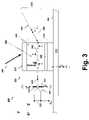
- FIG. 3is a highly-enlarged side view of the energy coupling device of FIG. 2( a );
- FIG. 4is a highly-enlarged perspective view of an energy coupling device illustrating the ultra-small micro-resonant structure according to alternate embodiments of the present invention
- FIG. 5is a highly-enlarged perspective view of an energy coupling device illustrating of the ultra-small micro-resonant structure according to alternate embodiments the present invention
- FIG. 6is a highly-enlarged top view of an energy coupling device illustrating of the ultra-small micro-resonant structure according to alternate embodiments the present invention.
- FIG. 7is a highly-enlarged top view of an energy coupling device showing of the ultra-small micro-resonant structure according to alternate embodiments of the present invention.
- the present inventionincludes devices and methods for coupling energy from an electromagnetic wave to charged particles.
- a surface of a micro-resonant structureis excited by energy from an electromagnetic wave, causing it to resonate. This resonant energy interacts as a varying field.
- a highly intensified electric field component of the varying fieldis coupled from the surface.
- a source of charged particlesreferred to herein as a beam, is provided.
- the beamcan include ions (positive or negative), electrons, protons and the like.
- the beammay be produced by any source, including, e.g., without limitation an ion gun, a tungsten filament, a cathode, a planar vacuum triode, an electron-impact ionizer, a laser ionizer, a chemical ionizer, a thermal ionizer, an ion-impact ionizer.
- the beamtravels on a path approaching the varying field.
- the beamis deflected or angularly modulated upon interacting with a varying field coupled from the surface. Hence, energy from the varying field is transferred to the charged particles of the beam.
- characteristics of the micro-resonant structure including shape, size and type of material disposed on the micro-resonant structurecan affect the intensity and wavelength of the varying field. Further, the intensity of the varying field can be increased by using features of the micro-resonant structure referred to as intensifiers. Further, the micro-resonant structure may include structures, nano-structures, sub-wavelength structures and the like. The device can include a plurality of micro-resonant structures having various orientations with respect to one another.
- FIG. 2( a )is a highly-enlarged perspective-view of an energy coupling device or device 200 showing an ultra-small micro-resonant structure (MRS) 202 having surfaces 204 for coupling energy of an electromagnetic wave 206 (also denoted E) to the MRS 202 in accordance with embodiments of the present invention.
- the MRS 202is formed on a major surface 208 of a substrate 210 , and, in the embodiments depicted in the drawing, is substantially C-shaped with a cavity 212 having a gap 216 , shown also in FIG. 2( b ).
- the MRS 202can be scaled in accordance with the (anticipated and/or desired) received wavelength of the electromagnetic wave 206 .
- the MRS 202is referred to as a sub-wavelength structure 214 when the size of the MRS 202 is on the order of one-quarter wavelength of the electromagnetic wave 206 .
- the height H of the MRS 202can be about 125 nanometers where the frequency of the electromagnetic wave 206 is about 600 terahertz.
- the MRS 202can be sized on the order of a quarter-wavelength multiple of the incident electromagnetic wave 206 .
- the surface 204 on the MRS 202is generally electrically conductive.
- materialssuch as gold (Au), copper (Cu), silver (Ag), and the like can be disposed on the surface 204 of the MRS 202 (or the MRS 202 can be formed substantially of such materials). Conductive alloys can also be used for these applications.
- Energy from electromagnetic wave 206is transferred to the surface 204 of the MRS 202 .
- the energy from the wave 218can be transferred to waves of electrons within the atomic structure on and adjacent to the surface 204 referred to as surface plasmons 220 (also denoted “P” in the drawing).
- the MRS 202stores the energy and resonates, thereby generating a varying field (denoted generally 222 ).
- the varying field 222can couple through a space 224 adjacent to the MRS 202 including the space 224 within the cavity 212 .
- a charged particle source 228emits a beam 226 of charged particles comprising, e.g., ions or electrons or positrons or the like.
- the charged particle source shown in FIG. 2( a )is a cathode 228 for emitting the beam 226 comprising electrons 230 .
- the charged particle sourcei.e., cathode 228
- the charged particle sourcecan be formed on the major surface 208 with the MRS 202 and, for example, can be coupled to a potential of minus V CC .
- the cathode 228can be made using a field emission tip, a thermionic source, and the like.
- the type and/or source of charged particle employedshould not be considered a limitation of the present invention.
- a control electrode 232is typically positioned between the cathode 228 and the MRS 202 .
- the beam 226is emitted from the cathode 228 , there can be a slight attraction by the electrons 230 to the control electrode 232 .
- a portion of the electrons 230travel through an opening 234 near the center of the control electrode 232 .
- the control electrode 232provides a narrow distribution of the beam 226 of electrons 230 that journey through the space 224 along a straight path 236 .
- the space 224should preferably be under a sufficient vacuum to prevent scattering of the electrons 230 .
- the electrons 230travel toward the cavity 212 along the straight path 236 . If no electromagnetic wave 206 is received on surface 204 , no varying field 222 is generated, and the electrons 230 travel generally along the straight path 236 undisturbed through the cavity 212 . In contrast, when an electromagnetic wave 206 is received, varying field 222 is generated. The varying field 222 couples through the space 224 within the cavity 212 . Hence, electrons 230 approaching the varying field 222 in the cavity 212 are deflected or angularly modulated from the straight path 236 to a plurality of paths (generally denoted 238 , not all shown).
- the varying field 222can comprise electric and magnetic field components (denoted ⁇ right arrow over (E) ⁇ and ⁇ right arrow over (B) ⁇ in FIG. 2( a )). It should be noted that varying electric and magnetic fields inherently occur together as taught by the well-known Maxwell's equations.
- the magnetic and electric fields within the cavity 212are generally along the X and Y axes of the coordinate system, respectively.
- An intensifieris used to increase the magnitude of the varying field 222 and particularly the electric field component of the varying field 222 . For example, as the distance across the gap 216 decreases, the electric field intensity typically increases across the gap 216 .
- the cavity 212is a particular form of an intensifier used to increase the magnitude of the varying field 222 .
- the force from the magnetic fieldacts on the electrons 230 generally in the same direction as the force from the electric field.
- FIG. 3is a highly-enlarged side-view of the device 200 from the exposed cavity 212 side of FIG. 2(A) illustrating angularly modulated electrons 230 in accordance with embodiments of the present invention.
- the cavity 212as shown, can extend the full length L of the MRS 202 and is exposed to the space 224 .
- the cavity 212can include a variety of shapes such as semi-circular, rectangular, triangular and the like.
- the varying field 222 formed across the gap 216provides a changing transverse force ⁇ right arrow over (F) ⁇ on the electrons.
- the electrons 230 traveling through the cavity 212can angularly modulate a plurality of times, thereby frequently changing directions from the forces of the varying field 222 .
- the electronscan travel on any one of the plurality of paths generally denoted 238 , including a generally sinusoidal path referred to as an oscillating path 242 .
- the electrons 230can travel on another one of the plurality of paths 238 referred to as a new path 244 , which is generally straight. Since the forces for angularly modulating the electrons 230 from the varying field 222 are generally within the cavity 212 , the electrons 230 typically no longer change direction after exiting the cavity 212 .
- the location of the new path 244 at a point in timecan be indicative of the amount of energy coupled from the electromagnetic wave 206 . For example, the further the beam 226 deflects from the straight path 236 , the greater the amount of energy from the electromagnetic wave 206 transferred to the beam 226 .
- the straight path 236is extended in the drawing to show an angle (denoted a) with respect to the new path 244 . Hence, the larger the angle ⁇ the greater the magnitude of energy transferred to the beam 226 .
- Angular modulationcan cause a portion of electrons 230 traveling in the cavity 212 to collide with the MRS 202 causing a charge to build up on the MRS 202 . If electrons 230 accumulate on the MRS 202 in sufficient number, the beam 226 can offset or bend away from the MRS 202 and from the varying field 222 coupled from the MRS 202 . This can diminish the interaction between the varying field 222 and the electrons 230 . For this reason, the MRS 202 is typically coupled to ground via a low resistive path to prevent any charge build-up on the MRS 202 . The grounding of the MRS 202 should not be considered a limitation of the present invention.
- FIG. 4is a highly-enlarged perspective-view illustrating a device 400 including alternate embodiments of a micro-resonant structure 402 .
- an electromagnetic wave 206also denoted E
- a gap 410 formed by ledge portions 412can act as an intensifier.
- the varying field 406is shown across the gap 410 with the electric and magnetic field components (denoted ⁇ right arrow over (E) ⁇ and ⁇ right arrow over (B) ⁇ ) generally along the X and Y axes of the coordinate system, respectively. Since a portion of the varying field can be intensified across the gap 410 , the ledge portions 412 can be sized during fabrication to provide a particular magnitude or wavelength of the varying field 406 .
- An external charged particle source 414targets a beam 416 of charged particles (e.g., electrons) along a straight path 420 through an opening 422 on a sidewall 424 of the device 400 .
- the charged particlestravel through a space 426 within the gap 410 .
- the charged particlesare shown angularly modulated, deflected or scattered from the straight path 420 .
- the charged particlestravel on an oscillating path 428 within the gap 410 .
- the charged particlesAfter passing through the gap 410 , the charged particles are angularly modulated on a new path 430 .
- An angle ⁇illustrates the deviation between the new path 430 and the straight path 420 .
- FIG. 5is a highly-enlarged perspective-view illustrating a device 500 according to alternate embodiments of the invention.
- the device 500includes a micro-resonant structure 502 .
- the MRS 502is formed by a wall 504 and is generally a semi-circular shape.
- the wall 504is connected to base portions 506 formed on a major surface 508 .
- energyis coupled from an electromagnetic wave (denoted E), and the MRS 502 resonates generating a varying field.
- An intensifier in the form here of a gap 512increases the magnitude of the varying field.
- a source of charged particlese.g., cathode 514 targets a beam 516 of electrons 518 on a straight path 520 .
- Interaction with the varying fieldcauses the beam 516 of electrons 518 to angularly modulate on exiting the cavity 522 to the new path 524 or any one of a plurality of paths generally denoted 526 (not all shown).
- FIG. 6is a highly-enlarged top-view illustrating a device 600 including yet another alternate embodiment of a micro-resonant structure 602 .
- the MRS 602 shown in the figureis generally a cube shaped structure, however those skilled in the art will immediately realize that the MRS need not be cube shaped and the invention is not limited by the shape of the MRS structure 602 .
- the MRSshould have some area to absorb the incoming photons and it should have some part of the structure having relatively sharp point, corner or cusp to concentrate the electric field near where the electron beam is traveling.
- the MRS 602may be shaped as a rectangle or triangle or needle or other shapes having the appropriate surface(s) and point(s). As described above with reference to FIG.
- the device 600may include a cathode 608 formed on the surface 610 for providing a beam 612 of electrons 614 along a path.
- the cathode 608directs the electrons 614 on a straight path 616 near an edge 618 of the MRS 602 , thereby providing an edge 618 for the intensifier.
- the electrons 614 approaching a space 620 near the edge 618are angularly modulated from the straight path 616 and form a new path 622 .
- the intensifiercan be a corner 624 of the MRS 602 , because the cathode 608 targets the beam 612 on a straight path 616 near the corner 624 of the MRS 602 .
- the electrons 614 approaching the corner 624are angularly modulated from the straight path 616 , thereby forming a new path 626 .
- the new paths 622 and 626can be any one path of the plurality of paths formed by the electrons on interacting with the varying field.
- the intensifiermay be a protuberance or boss that protrudes or is generally elevated above a surface 628 of the MRS 602 .
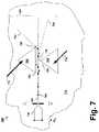
- FIG. 7is a highly-enlarged view illustrating a device 700 including yet other alternate embodiments of micro-resonant structures according to the present invention.
- the MRS 702comprises a plurality of structures 704 and 706 , which are, in preferred embodiments, generally triangular shaped, although the shape of the structures 704 and 706 can include a variety of shapes including rectangular, spherical, cylindrical, cubic and the like. The invention is not limited by the shape of the structures 704 and 706 .
- the MRSreceives the electromagnetic wave 712 (also denoted E).
- the MRSgenerates a varying field (denoted 716 ) that is magnified using an intensifier.
- the intensifierincludes corners 720 and 722 of the structure 704 and corner 724 of the structure 706 .
- the cathode 726provides a beam 728 of electrons 704 approaching the varying field 716 along the straight path 708 .
- the electrons 704are deflected or angularly modulated from a straight path 708 at corners 720 , 722 and 724 , to travel along one of a plurality of paths (denoted 730 ), e.g., along the path referred to as a new path 732 .
- the intensifier of the varying fieldmay be a gap between structures 704 and 706 .
- the varying field across the gapangularly modulates the beam 728 to a new path 736 , which is one of the plurality of paths generally denoted 730 (not all shown).
- devices having a micro-resonant structure and that couple energy from electromagnetic waveshave been provided. Further, methods of angularly modulating charged particles on receiving an electromagnetic wave have been provided. Energy from the electromagnetic wave is coupled to the micro-resonant structure and a varying field is generated.
- a charged particle sourceprovides a first path of electrons that travel toward a cavity of the micro-resonant structure containing the varying field. The electrons are deflected or angularly modulated from the first path to a second path on interacting with the varying field.
- the micro-resonant structurecan include a range of shapes and sizes. Further, the micro-resonant structure can include structures, nano-structures, sub-wavelength structures and the like. The device provides the advantage of using the same basic structure to cover the full terahertz frequency spectrum.
Landscapes
- Optical Modulation, Optical Deflection, Nonlinear Optics, Optical Demodulation, Optical Logic Elements (AREA)
- Analysing Materials By The Use Of Radiation (AREA)
- Cold Cathode And The Manufacture (AREA)
- Crystals, And After-Treatments Of Crystals (AREA)
- Electron Sources, Ion Sources (AREA)
- Particle Accelerators (AREA)
Abstract
Description
| Type | Approx. Frequency | ||
| Radio | Less than 3 Gigahertz | ||
| Microwave | 3 Gigahertz–300 Gigahertz | ||
| Infrared | 300 Gigahertz–400 Terahertz | ||
| Visible | 400 Terahertz–750 Terahertz | ||
| UV | 750 Terahertz–30 Petahertz | ||
| X-ray | 30 Petahertz–30 Exahertz | ||
| Gamma-ray | Greater than 30 Exahertz | ||
Claims (48)
Priority Applications (6)
| Application Number | Priority Date | Filing Date | Title |
|---|---|---|---|
| US11/243,476US7253426B2 (en) | 2005-09-30 | 2005-10-05 | Structures and methods for coupling energy from an electromagnetic wave |
| PCT/US2006/022771WO2007064358A2 (en) | 2005-09-30 | 2006-06-12 | Structures and methods for coupling energy from an electromagnetic wave |
| TW095121880ATW200713381A (en) | 2005-09-30 | 2006-06-19 | Structures and methods for coupling energy from an electromagnetic wave |
| US11/716,552US7557365B2 (en) | 2005-09-30 | 2007-03-12 | Structures and methods for coupling energy from an electromagnetic wave |
| US13/774,593US9076623B2 (en) | 2004-08-13 | 2013-02-22 | Switching micro-resonant structures by modulating a beam of charged particles |
| US14/487,263US20150001424A1 (en) | 2004-08-13 | 2014-09-16 | Switching micro-resonant structures by modulating a beam of charged particles |
Applications Claiming Priority (2)
| Application Number | Priority Date | Filing Date | Title |
|---|---|---|---|
| US11/238,991US7791290B2 (en) | 2005-09-30 | 2005-09-30 | Ultra-small resonating charged particle beam modulator |
| US11/243,476US7253426B2 (en) | 2005-09-30 | 2005-10-05 | Structures and methods for coupling energy from an electromagnetic wave |
Related Parent Applications (1)
| Application Number | Title | Priority Date | Filing Date |
|---|---|---|---|
| US11/238,991Continuation-In-PartUS7791290B2 (en) | 2004-08-13 | 2005-09-30 | Ultra-small resonating charged particle beam modulator |
Related Child Applications (1)
| Application Number | Title | Priority Date | Filing Date |
|---|---|---|---|
| US11/716,552ContinuationUS7557365B2 (en) | 2005-09-30 | 2007-03-12 | Structures and methods for coupling energy from an electromagnetic wave |
Publications (2)
| Publication Number | Publication Date |
|---|---|
| US20070085039A1 US20070085039A1 (en) | 2007-04-19 |
| US7253426B2true US7253426B2 (en) | 2007-08-07 |
Family
ID=37901012
Family Applications (3)
| Application Number | Title | Priority Date | Filing Date |
|---|---|---|---|
| US11/238,991Expired - LifetimeUS7791290B2 (en) | 2004-08-13 | 2005-09-30 | Ultra-small resonating charged particle beam modulator |
| US11/243,476Expired - Fee RelatedUS7253426B2 (en) | 2004-08-13 | 2005-10-05 | Structures and methods for coupling energy from an electromagnetic wave |
| US11/418,263Active - Reinstated2027-09-28US7791291B2 (en) | 2005-09-30 | 2006-05-05 | Diamond field emission tip and a method of formation |
Family Applications Before (1)
| Application Number | Title | Priority Date | Filing Date |
|---|---|---|---|
| US11/238,991Expired - LifetimeUS7791290B2 (en) | 2004-08-13 | 2005-09-30 | Ultra-small resonating charged particle beam modulator |
Family Applications After (1)
| Application Number | Title | Priority Date | Filing Date |
|---|---|---|---|
| US11/418,263Active - Reinstated2027-09-28US7791291B2 (en) | 2005-09-30 | 2006-05-05 | Diamond field emission tip and a method of formation |
Country Status (3)
| Country | Link |
|---|---|
| US (3) | US7791290B2 (en) |
| TW (3) | TW200713381A (en) |
| WO (1) | WO2007040672A2 (en) |
Cited By (45)
| Publication number | Priority date | Publication date | Assignee | Title |
|---|---|---|---|---|
| US20060022151A1 (en)* | 2004-07-30 | 2006-02-02 | Advanced Energy Systems, Inc. | System and method for producing Terahertz radiation |
| US20070139646A1 (en)* | 2005-12-16 | 2007-06-21 | Asml Netherlands B.V. | Lithographic apparatus and method |
| US20070170370A1 (en)* | 2005-09-30 | 2007-07-26 | Virgin Islands Microsystems, Inc. | Structures and methods for coupling energy from an electromagnetic wave |
| US20070184874A1 (en)* | 2004-07-06 | 2007-08-09 | Seiko Epson Corporation | Electronic apparatus and wireless communication terminal |
| US20080245976A1 (en)* | 2007-04-04 | 2008-10-09 | Bernard John Eastlund | Projector Lamp having Pulsed Monochromatic Microwave Light Sources |
| US20090027280A1 (en)* | 2005-05-05 | 2009-01-29 | Frangioni John V | Micro-scale resonant devices and methods of use |
| US20090125254A1 (en)* | 2007-11-13 | 2009-05-14 | Battelle Energy Alliance, Llc | Methods, computer readable media, and graphical user interfaces for analysis of frequency selective surfaces |
| US7554083B2 (en) | 2006-05-05 | 2009-06-30 | Virgin Islands Microsystems, Inc. | Integration of electromagnetic detector on integrated chip |
| US7558490B2 (en) | 2006-04-10 | 2009-07-07 | Virgin Islands Microsystems, Inc. | Resonant detector for optical signals |
| US7557647B2 (en) | 2006-05-05 | 2009-07-07 | Virgin Islands Microsystems, Inc. | Heterodyne receiver using resonant structures |
| US7560716B2 (en)* | 2006-09-22 | 2009-07-14 | Virgin Islands Microsystems, Inc. | Free electron oscillator |
| US7569836B2 (en) | 2006-05-05 | 2009-08-04 | Virgin Islands Microsystems, Inc. | Transmission of data between microchips using a particle beam |
| US7573045B2 (en) | 2006-05-15 | 2009-08-11 | Virgin Islands Microsystems, Inc. | Plasmon wave propagation devices and methods |
| US7579609B2 (en) | 2005-12-14 | 2009-08-25 | Virgin Islands Microsystems, Inc. | Coupling light of light emitting resonator to waveguide |
| US7583370B2 (en) | 2006-05-05 | 2009-09-01 | Virgin Islands Microsystems, Inc. | Resonant structures and methods for encoding signals into surface plasmons |
| US7586097B2 (en) | 2006-01-05 | 2009-09-08 | Virgin Islands Microsystems, Inc. | Switching micro-resonant structures using at least one director |
| US7586167B2 (en) | 2006-05-05 | 2009-09-08 | Virgin Islands Microsystems, Inc. | Detecting plasmons using a metallurgical junction |
| US7605835B2 (en) | 2006-02-28 | 2009-10-20 | Virgin Islands Microsystems, Inc. | Electro-photographic devices incorporating ultra-small resonant structures |
| US7619373B2 (en) | 2006-01-05 | 2009-11-17 | Virgin Islands Microsystems, Inc. | Selectable frequency light emitter |
| US7626179B2 (en) | 2005-09-30 | 2009-12-01 | Virgin Island Microsystems, Inc. | Electron beam induced resonance |
| US7646991B2 (en) | 2006-04-26 | 2010-01-12 | Virgin Island Microsystems, Inc. | Selectable frequency EMR emitter |
| US7656094B2 (en) | 2006-05-05 | 2010-02-02 | Virgin Islands Microsystems, Inc. | Electron accelerator for ultra-small resonant structures |
| US7655934B2 (en) | 2006-06-28 | 2010-02-02 | Virgin Island Microsystems, Inc. | Data on light bulb |
| US7659513B2 (en) | 2006-12-20 | 2010-02-09 | Virgin Islands Microsystems, Inc. | Low terahertz source and detector |
| US7679067B2 (en) | 2006-05-26 | 2010-03-16 | Virgin Island Microsystems, Inc. | Receiver array using shared electron beam |
| US7688274B2 (en) | 2006-02-28 | 2010-03-30 | Virgin Islands Microsystems, Inc. | Integrated filter in antenna-based detector |
| US7710040B2 (en) | 2006-05-05 | 2010-05-04 | Virgin Islands Microsystems, Inc. | Single layer construction for ultra small devices |
| US7718977B2 (en) | 2006-05-05 | 2010-05-18 | Virgin Island Microsystems, Inc. | Stray charged particle removal device |
| US7723698B2 (en) | 2006-05-05 | 2010-05-25 | Virgin Islands Microsystems, Inc. | Top metal layer shield for ultra-small resonant structures |
| US7728397B2 (en) | 2006-05-05 | 2010-06-01 | Virgin Islands Microsystems, Inc. | Coupled nano-resonating energy emitting structures |
| US7728702B2 (en) | 2006-05-05 | 2010-06-01 | Virgin Islands Microsystems, Inc. | Shielding of integrated circuit package with high-permeability magnetic material |
| US7732786B2 (en) | 2006-05-05 | 2010-06-08 | Virgin Islands Microsystems, Inc. | Coupling energy in a plasmon wave to an electron beam |
| US7741934B2 (en) | 2006-05-05 | 2010-06-22 | Virgin Islands Microsystems, Inc. | Coupling a signal through a window |
| US7746532B2 (en) | 2006-05-05 | 2010-06-29 | Virgin Island Microsystems, Inc. | Electro-optical switching system and method |
| US7791290B2 (en) | 2005-09-30 | 2010-09-07 | Virgin Islands Microsystems, Inc. | Ultra-small resonating charged particle beam modulator |
| US7791053B2 (en) | 2007-10-10 | 2010-09-07 | Virgin Islands Microsystems, Inc. | Depressed anode with plasmon-enabled devices such as ultra-small resonant structures |
| US20100284086A1 (en)* | 2007-11-13 | 2010-11-11 | Battelle Energy Alliance, Llc | Structures, systems and methods for harvesting energy from electromagnetic radiation |
| US7876793B2 (en) | 2006-04-26 | 2011-01-25 | Virgin Islands Microsystems, Inc. | Micro free electron laser (FEL) |
| US7986113B2 (en) | 2006-05-05 | 2011-07-26 | Virgin Islands Microsystems, Inc. | Selectable frequency light emitter |
| US7990336B2 (en) | 2007-06-19 | 2011-08-02 | Virgin Islands Microsystems, Inc. | Microwave coupled excitation of solid state resonant arrays |
| US8188431B2 (en) | 2006-05-05 | 2012-05-29 | Jonathan Gorrell | Integration of vacuum microelectronic device with integrated circuit |
| US8847824B2 (en) | 2012-03-21 | 2014-09-30 | Battelle Energy Alliance, Llc | Apparatuses and method for converting electromagnetic radiation to direct current |
| US9472699B2 (en) | 2007-11-13 | 2016-10-18 | Battelle Energy Alliance, Llc | Energy harvesting devices, systems, and related methods |
| WO2019108886A1 (en)* | 2017-12-01 | 2019-06-06 | At&T Intellectual Property I, L.P. | Apparatus and method for guided wave communications using an absorber |
| US20230008065A1 (en)* | 2021-07-07 | 2023-01-12 | Triseka, Inc. | Light Source for High Power Coherent Light, Imaging System, and Method of Using Relativistic Electrons for Imaging and Treatment |
Families Citing this family (15)
| Publication number | Priority date | Publication date | Assignee | Title |
|---|---|---|---|---|
| US20070190794A1 (en)* | 2006-02-10 | 2007-08-16 | Virgin Islands Microsystems, Inc. | Conductive polymers for the electroplating |
| US20070200646A1 (en)* | 2006-02-28 | 2007-08-30 | Virgin Island Microsystems, Inc. | Method for coupling out of a magnetic device |
| US20070200063A1 (en)* | 2006-02-28 | 2007-08-30 | Virgin Islands Microsystems, Inc. | Wafer-level testing of light-emitting resonant structures |
| US20070264023A1 (en)* | 2006-04-26 | 2007-11-15 | Virgin Islands Microsystems, Inc. | Free space interchip communications |
| US20070252089A1 (en)* | 2006-04-26 | 2007-11-01 | Virgin Islands Microsystems, Inc. | Charged particle acceleration apparatus and method |
| US20070258720A1 (en)* | 2006-05-05 | 2007-11-08 | Virgin Islands Microsystems, Inc. | Inter-chip optical communication |
| US20070257273A1 (en)* | 2006-05-05 | 2007-11-08 | Virgin Island Microsystems, Inc. | Novel optical cover for optical chip |
| JP2010277942A (en)* | 2009-06-01 | 2010-12-09 | Mitsubishi Electric Corp | H-mode drift tube linear accelerator and its electric field distribution adjusting method |
| US9764160B2 (en) | 2011-12-27 | 2017-09-19 | HJ Laboratories, LLC | Reducing absorption of radiation by healthy cells from an external radiation source |
| WO2013119612A1 (en)* | 2012-02-07 | 2013-08-15 | Board Of Trustees Of Michigan State University | Electron microscope |
| US8519644B1 (en)* | 2012-08-15 | 2013-08-27 | Transmute, Inc. | Accelerator having acceleration channels formed between covalently bonded chips |
| US9966161B2 (en)* | 2015-09-21 | 2018-05-08 | Uchicago Argonne, Llc | Mechanical design of thin-film diamond crystal mounting apparatus with optimized thermal contact and crystal strain for coherence preservation x-ray optics |
| EP3402598A4 (en)* | 2016-01-13 | 2019-08-21 | William Fitzhugh | Methods and systems for separating carbon nanotubes |
| KR102640203B1 (en) | 2016-06-24 | 2024-02-23 | 삼성전자주식회사 | Optical device including slot and apparatus employing the optical device |
| CN110160573B (en)* | 2019-07-08 | 2022-03-25 | 山东省科学院激光研究所 | Escholtz ultrafast modulation pulse scanning laser and distributed optical fiber sensing system |
Citations (41)
| Publication number | Priority date | Publication date | Assignee | Title |
|---|---|---|---|---|
| US2634372A (en) | 1953-04-07 | Super high-frequency electromag | ||
| US3923568A (en) | 1974-01-14 | 1975-12-02 | Int Plasma Corp | Dry plasma process for etching noble metal |
| WO1987001873A1 (en) | 1985-09-19 | 1987-03-26 | Hughes Aircraft Company | Radiation source |
| US4740973A (en) | 1984-05-21 | 1988-04-26 | Madey John M J | Free electron laser |
| US4829527A (en) | 1984-04-23 | 1989-05-09 | The United States Of America As Represented By The Secretary Of The Army | Wideband electronic frequency tuning for orotrons |
| US5157000A (en) | 1989-07-10 | 1992-10-20 | Texas Instruments Incorporated | Method for dry etching openings in integrated circuit layers |
| US5185073A (en) | 1988-06-21 | 1993-02-09 | International Business Machines Corporation | Method of fabricating nendritic materials |
| WO1993021663A1 (en) | 1992-04-08 | 1993-10-28 | Georgia Tech Research Corporation | Process for lift-off of thin film materials from a growth substrate |
| US5263043A (en) | 1990-08-31 | 1993-11-16 | Trustees Of Dartmouth College | Free electron laser utilizing grating coupling |
| US5302240A (en) | 1991-01-22 | 1994-04-12 | Kabushiki Kaisha Toshiba | Method of manufacturing semiconductor device |
| US5668368A (en) | 1992-02-21 | 1997-09-16 | Hitachi, Ltd. | Apparatus for suppressing electrification of sample in charged beam irradiation apparatus |
| US5705443A (en) | 1995-05-30 | 1998-01-06 | Advanced Technology Materials, Inc. | Etching method for refractory materials |
| US5744919A (en) | 1996-12-12 | 1998-04-28 | Mishin; Andrey V. | CW particle accelerator with low particle injection velocity |
| US5757009A (en) | 1996-12-27 | 1998-05-26 | Northrop Grumman Corporation | Charged particle beam expander |
| US5767013A (en) | 1996-08-26 | 1998-06-16 | Lg Semicon Co., Ltd. | Method for forming interconnection in semiconductor pattern device |
| US5790585A (en) | 1996-11-12 | 1998-08-04 | The Trustees Of Dartmouth College | Grating coupling free electron laser apparatus and method |
| US5831270A (en) | 1996-02-19 | 1998-11-03 | Nikon Corporation | Magnetic deflectors and charged-particle-beam lithography systems incorporating same |
| US6040625A (en) | 1997-09-25 | 2000-03-21 | I/O Sensors, Inc. | Sensor package arrangement |
| US6060833A (en) | 1996-10-18 | 2000-05-09 | Velazco; Jose E. | Continuous rotating-wave electron beam accelerator |
| US6080529A (en) | 1997-12-12 | 2000-06-27 | Applied Materials, Inc. | Method of etching patterned layers useful as masking during subsequent etching or for damascene structures |
| WO2000072413A2 (en) | 1999-05-25 | 2000-11-30 | Deutsche Telekom Ag | Miniaturized terahertz radiation source |
| US6195199B1 (en)* | 1997-10-27 | 2001-02-27 | Kanazawa University | Electron tube type unidirectional optical amplifier |
| US20010025925A1 (en) | 2000-03-28 | 2001-10-04 | Kabushiki Kaisha Toshiba | Charged particle beam system and pattern slant observing method |
| WO2002025785A2 (en) | 2000-09-22 | 2002-03-28 | Vermont Photonics | Apparatuses and methods for generating coherent electromagnetic laser radiation |
| US6370306B1 (en) | 1997-12-15 | 2002-04-09 | Seiko Instruments Inc. | Optical waveguide probe and its manufacturing method |
| US6373194B1 (en) | 2000-06-01 | 2002-04-16 | Raytheon Company | Optical magnetron for high efficiency production of optical radiation |
| WO2002077607A2 (en) | 2001-03-23 | 2002-10-03 | Vermont Photonics | Applying far infrared radiation to biological matter |
| US20030012925A1 (en) | 2001-07-16 | 2003-01-16 | Motorola, Inc. | Process for fabricating semiconductor structures and devices utilizing the formation of a compliant substrate for materials used to form the same and including an etch stop layer used for back side processing |
| JP2004032323A (en) | 2002-06-25 | 2004-01-29 | Toyo Commun Equip Co Ltd | Surface mounting type piezoelectric oscillator and its manufacturing method |
| US20040108473A1 (en) | 2000-06-09 | 2004-06-10 | Melnychuk Stephan T. | Extreme ultraviolet light source |
| US20040171272A1 (en) | 2003-02-28 | 2004-09-02 | Applied Materials, Inc. | Method of etching metallic materials to form a tapered profile |
| US20040213375A1 (en) | 2003-04-25 | 2004-10-28 | Paul Bjorkholm | Radiation sources and radiation scanning systems with improved uniformity of radiation intensity |
| US20040231996A1 (en) | 2003-05-20 | 2004-11-25 | Novellus Systems, Inc. | Electroplating using DC current interruption and variable rotation rate |
| US20050023145A1 (en) | 2003-05-07 | 2005-02-03 | Microfabrica Inc. | Methods and apparatus for forming multi-layer structures using adhered masks |
| WO2005015143A2 (en) | 2003-08-11 | 2005-02-17 | Opgal Ltd. | Radiometry using an uncooled microbolometer detector |
| US20050067286A1 (en) | 2003-09-26 | 2005-03-31 | The University Of Cincinnati | Microfabricated structures and processes for manufacturing same |
| US6885262B2 (en) | 2002-11-05 | 2005-04-26 | Ube Industries, Ltd. | Band-pass filter using film bulk acoustic resonator |
| US20050194258A1 (en) | 2003-06-27 | 2005-09-08 | Microfabrica Inc. | Electrochemical fabrication methods incorporating dielectric materials and/or using dielectric substrates |
| US20060035173A1 (en) | 2004-08-13 | 2006-02-16 | Mark Davidson | Patterning thin metal films by dry reactive ion etching |
| US20060062258A1 (en) | 2004-07-02 | 2006-03-23 | Vanderbilt University | Smith-Purcell free electron laser and method of operating same |
| US7122978B2 (en) | 2004-04-19 | 2006-10-17 | Mitsubishi Denki Kabushiki Kaisha | Charged-particle beam accelerator, particle beam radiation therapy system using the charged-particle beam accelerator, and method of operating the particle beam radiation therapy system |
Family Cites Families (282)
| Publication number | Priority date | Publication date | Assignee | Title |
|---|---|---|---|---|
| US1948384A (en)* | 1932-01-26 | 1934-02-20 | Research Corp | Method and apparatus for the acceleration of ions |
| US2307086A (en)* | 1941-05-07 | 1943-01-05 | Univ Leland Stanford Junior | High frequency electrical apparatus |
| US2431396A (en) | 1942-12-21 | 1947-11-25 | Rca Corp | Current magnitude-ratio responsive amplifier |
| US2397905A (en)* | 1944-08-07 | 1946-04-09 | Int Harvester Co | Thrust collar construction |
| US2473477A (en) | 1946-07-24 | 1949-06-14 | Raythcon Mfg Company | Magnetic induction device |
| US2932798A (en)* | 1956-01-05 | 1960-04-12 | Research Corp | Imparting energy to charged particles |
| US2944183A (en) | 1957-01-25 | 1960-07-05 | Bell Telephone Labor Inc | Internal cavity reflex klystron tuned by a tightly coupled external cavity |
| US2966611A (en) | 1959-07-21 | 1960-12-27 | Sperry Rand Corp | Ruggedized klystron tuner |
| US3231779A (en)* | 1962-06-25 | 1966-01-25 | Gen Electric | Elastic wave responsive apparatus |
| US3274428A (en) | 1962-06-29 | 1966-09-20 | English Electric Valve Co Ltd | Travelling wave tube with band pass slow wave structure whose frequency characteristic changes along its length |
| GB1054461A (en)* | 1963-02-06 | |||
| US3315117A (en)* | 1963-07-15 | 1967-04-18 | Burton J Udelson | Electrostatically focused electron beam phase shifter |
| US3387169A (en) | 1965-05-07 | 1968-06-04 | Sfd Lab Inc | Slow wave structure of the comb type having strap means connecting the teeth to form iterative inductive shunt loadings |
| US4746201A (en) | 1967-03-06 | 1988-05-24 | Gordon Gould | Polarizing apparatus employing an optical element inclined at brewster's angle |
| US4053845A (en) | 1967-03-06 | 1977-10-11 | Gordon Gould | Optically pumped laser amplifiers |
| US3546524A (en) | 1967-11-24 | 1970-12-08 | Varian Associates | Linear accelerator having the beam injected at a position of maximum r.f. accelerating field |
| US3571642A (en)* | 1968-01-17 | 1971-03-23 | Ca Atomic Energy Ltd | Method and apparatus for interleaved charged particle acceleration |
| US3543147A (en) | 1968-03-29 | 1970-11-24 | Atomic Energy Commission | Phase angle measurement system for determining and controlling the resonance of the radio frequency accelerating cavities for high energy charged particle accelerators |
| US3586899A (en) | 1968-06-12 | 1971-06-22 | Ibm | Apparatus using smith-purcell effect for frequency modulation and beam deflection |
| US3560694A (en)* | 1969-01-21 | 1971-02-02 | Varian Associates | Microwave applicator employing flat multimode cavity for treating webs |
| US3761828A (en) | 1970-12-10 | 1973-09-25 | J Pollard | Linear particle accelerator with coast through shield |
| US3886399A (en) | 1973-08-20 | 1975-05-27 | Varian Associates | Electron beam electrical power transmission system |
| DE2429612C2 (en) | 1974-06-20 | 1984-08-02 | Siemens AG, 1000 Berlin und 8000 München | Acousto-optical data input converter for block-organized holographic data storage and method for its control |
| US4704583A (en) | 1974-08-16 | 1987-11-03 | Gordon Gould | Light amplifiers employing collisions to produce a population inversion |
| JPS6056238B2 (en) | 1979-06-01 | 1985-12-09 | 株式会社井上ジャパックス研究所 | Electroplating method |
| US4296354A (en) | 1979-11-28 | 1981-10-20 | Varian Associates, Inc. | Traveling wave tube with frequency variable sever length |
| US4282436A (en) | 1980-06-04 | 1981-08-04 | The United States Of America As Represented By The Secretary Of The Navy | Intense ion beam generation with an inverse reflex tetrode (IRT) |
| US4453108A (en) | 1980-11-21 | 1984-06-05 | William Marsh Rice University | Device for generating RF energy from electromagnetic radiation of another form such as light |
| US4661783A (en)* | 1981-03-18 | 1987-04-28 | The United States Of America As Represented By The Secretary Of The Navy | Free electron and cyclotron resonance distributed feedback lasers and masers |
| US4450554A (en) | 1981-08-10 | 1984-05-22 | International Telephone And Telegraph Corporation | Asynchronous integrated voice and data communication system |
| US4528659A (en) | 1981-12-17 | 1985-07-09 | International Business Machines Corporation | Interleaved digital data and voice communications system apparatus and method |
| US4589107A (en) | 1982-11-30 | 1986-05-13 | Itt Corporation | Simultaneous voice and data communication and data base access in a switching system using a combined voice conference and data base processing module |
| US4652703A (en)* | 1983-03-01 | 1987-03-24 | Racal Data Communications Inc. | Digital voice transmission having improved echo suppression |
| US4482779A (en) | 1983-04-19 | 1984-11-13 | The United States Of America As Represented By The Administrator Of National Aeronautics And Space Administration | Inelastic tunnel diodes |
| US4598397A (en) | 1984-02-21 | 1986-07-01 | Cxc Corporation | Microtelephone controller |
| US4713581A (en) | 1983-08-09 | 1987-12-15 | Haimson Research Corporation | Method and apparatus for accelerating a particle beam |
| DE3479468D1 (en) | 1984-05-23 | 1989-09-21 | Ibm | Digital transmission system for a packetized voice |
| US4819228A (en)* | 1984-10-29 | 1989-04-04 | Stratacom Inc. | Synchronous packet voice/data communication system |
| GB2171576B (en) | 1985-02-04 | 1989-07-12 | Mitel Telecom Ltd | Spread spectrum leaky feeder communication system |
| US4675863A (en)* | 1985-03-20 | 1987-06-23 | International Mobile Machines Corp. | Subscriber RF telephone system for providing multiple speech and/or data signals simultaneously over either a single or a plurality of RF channels |
| JPS6229135A (en) | 1985-07-29 | 1987-02-07 | Advantest Corp | Charged particle beam exposure and device thereof |
| IL79775A (en) | 1985-08-23 | 1990-06-10 | Republic Telcom Systems Corp | Multiplexed digital packet telephone system |
| US4740963A (en)* | 1986-01-30 | 1988-04-26 | Lear Siegler, Inc. | Voice and data communication system |
| US4712042A (en) | 1986-02-03 | 1987-12-08 | Accsys Technology, Inc. | Variable frequency RFQ linear accelerator |
| JPS62142863U (en) | 1986-03-05 | 1987-09-09 | ||
| JPH0763171B2 (en) | 1986-06-10 | 1995-07-05 | 株式会社日立製作所 | Data / voice transmission / reception method |
| US4761059A (en) | 1986-07-28 | 1988-08-02 | Rockwell International Corporation | External beam combining of multiple lasers |
| US4813040A (en)* | 1986-10-31 | 1989-03-14 | Futato Steven P | Method and apparatus for transmitting digital data and real-time digitalized voice information over a communications channel |
| US5163118A (en) | 1986-11-10 | 1992-11-10 | The United States Of America As Represented By The Secretary Of The Air Force | Lattice mismatched hetrostructure optical waveguide |
| JPH07118749B2 (en)* | 1986-11-14 | 1995-12-18 | 株式会社日立製作所 | Voice / data transmission equipment |
| US4806859A (en)* | 1987-01-27 | 1989-02-21 | Ford Motor Company | Resonant vibrating structures with driving sensing means for noncontacting position and pick up sensing |
| US4898022A (en)* | 1987-02-09 | 1990-02-06 | Tlv Co., Ltd. | Steam trap operation detector |
| US4932022A (en) | 1987-10-07 | 1990-06-05 | Telenova, Inc. | Integrated voice and data telephone system |
| US4864131A (en) | 1987-11-09 | 1989-09-05 | The University Of Michigan | Positron microscopy |
| US4838021A (en) | 1987-12-11 | 1989-06-13 | Hughes Aircraft Company | Electrostatic ion thruster with improved thrust modulation |
| US4890282A (en) | 1988-03-08 | 1989-12-26 | Network Equipment Technologies, Inc. | Mixed mode compression for data transmission |
| US4866704A (en) | 1988-03-16 | 1989-09-12 | California Institute Of Technology | Fiber optic voice/data network |
| US4887265A (en) | 1988-03-18 | 1989-12-12 | Motorola, Inc. | Packet-switched cellular telephone system |
| JPH0744511B2 (en) | 1988-09-14 | 1995-05-15 | 富士通株式会社 | High suburb rate multiplexing method |
| US5130985A (en) | 1988-11-25 | 1992-07-14 | Hitachi, Ltd. | Speech packet communication system and method |
| FR2641093B1 (en) | 1988-12-23 | 1994-04-29 | Alcatel Business Systems | |
| US4981371A (en)* | 1989-02-17 | 1991-01-01 | Itt Corporation | Integrated I/O interface for communication terminal |
| US5023563A (en) | 1989-06-08 | 1991-06-11 | Hughes Aircraft Company | Upshifted free electron laser amplifier |
| US5036513A (en) | 1989-06-21 | 1991-07-30 | Academy Of Applied Science | Method of and apparatus for integrated voice (audio) communication simultaneously with "under voice" user-transparent digital data between telephone instruments |
| US5155726A (en) | 1990-01-22 | 1992-10-13 | Digital Equipment Corporation | Station-to-station full duplex communication in a token ring local area network |
| US5235248A (en) | 1990-06-08 | 1993-08-10 | The United States Of America As Represented By The United States Department Of Energy | Method and split cavity oscillator/modulator to generate pulsed particle beams and electromagnetic fields |
| US5127001A (en) | 1990-06-22 | 1992-06-30 | Unisys Corporation | Conference call arrangement for distributed network |
| US5113141A (en) | 1990-07-18 | 1992-05-12 | Science Applications International Corporation | Four-fingers RFQ linac structure |
| US5268693A (en) | 1990-08-31 | 1993-12-07 | Trustees Of Dartmouth College | Semiconductor film free electron laser |
| US5128729A (en) | 1990-11-13 | 1992-07-07 | Motorola, Inc. | Complex opto-isolator with improved stand-off voltage stability |
| US5214650A (en) | 1990-11-19 | 1993-05-25 | Ag Communication Systems Corporation | Simultaneous voice and data system using the existing two-wire inter-face |
| US5187591A (en)* | 1991-01-24 | 1993-02-16 | Micom Communications Corp. | System for transmitting and receiving aural information and modulated data |
| US5341374A (en) | 1991-03-01 | 1994-08-23 | Trilan Systems Corporation | Communication network integrating voice data and video with distributed call processing |
| US5150410A (en) | 1991-04-11 | 1992-09-22 | Itt Corporation | Secure digital conferencing system |
| US5283819A (en)* | 1991-04-25 | 1994-02-01 | Compuadd Corporation | Computing and multimedia entertainment system |
| FR2677490B1 (en) | 1991-06-07 | 1997-05-16 | Thomson Csf | SEMICONDUCTOR OPTICAL TRANSCEIVER. |
| GB9113684D0 (en) | 1991-06-25 | 1991-08-21 | Smiths Industries Plc | Display filter arrangements |
| US5229782A (en)* | 1991-07-19 | 1993-07-20 | Conifer Corporation | Stacked dual dipole MMDS feed |
| US5199918A (en)* | 1991-11-07 | 1993-04-06 | Microelectronics And Computer Technology Corporation | Method of forming field emitter device with diamond emission tips |
| US5305312A (en)* | 1992-02-07 | 1994-04-19 | At&T Bell Laboratories | Apparatus for interfacing analog telephones and digital data terminals to an ISDN line |
| WO1993018428A2 (en) | 1992-03-13 | 1993-09-16 | Kopin Corporation | Head-mounted display system |
| US5233623A (en) | 1992-04-29 | 1993-08-03 | Research Foundation Of State University Of New York | Integrated semiconductor laser with electronic directivity and focusing control |
| US5282197A (en)* | 1992-05-15 | 1994-01-25 | International Business Machines | Low frequency audio sub-channel embedded signalling |
| US5562838A (en)* | 1993-03-29 | 1996-10-08 | Martin Marietta Corporation | Optical light pipe and microwave waveguide interconnects in multichip modules formed using adaptive lithography |
| US5539414A (en) | 1993-09-02 | 1996-07-23 | Inmarsat | Folded dipole microstrip antenna |
| TW255015B (en) | 1993-11-05 | 1995-08-21 | Motorola Inc | |
| US5578909A (en) | 1994-07-15 | 1996-11-26 | The Regents Of The Univ. Of California | Coupled-cavity drift-tube linac |
| US5485277A (en)* | 1994-07-26 | 1996-01-16 | Physical Optics Corporation | Surface plasmon resonance sensor and methods for the utilization thereof |
| US5608263A (en)* | 1994-09-06 | 1997-03-04 | The Regents Of The University Of Michigan | Micromachined self packaged circuits for high-frequency applications |
| JP2770755B2 (en) | 1994-11-16 | 1998-07-02 | 日本電気株式会社 | Field emission type electron gun |
| US5637966A (en) | 1995-02-06 | 1997-06-10 | The Regents Of The University Of Michigan | Method for generating a plasma wave to accelerate electrons |
| US5504341A (en)* | 1995-02-17 | 1996-04-02 | Zimec Consulting, Inc. | Producing RF electric fields suitable for accelerating atomic and molecular ions in an ion implantation system |
| JP2921430B2 (en) | 1995-03-03 | 1999-07-19 | 双葉電子工業株式会社 | Optical writing element |
| US5604352A (en)* | 1995-04-25 | 1997-02-18 | Raychem Corporation | Apparatus comprising voltage multiplication components |
| US5858799A (en)* | 1995-10-25 | 1999-01-12 | University Of Washington | Surface plasmon resonance chemical electrode |
| JP3487699B2 (en)* | 1995-11-08 | 2004-01-19 | 株式会社日立製作所 | Ultrasonic treatment method and apparatus |
| US5889449A (en)* | 1995-12-07 | 1999-03-30 | Space Systems/Loral, Inc. | Electromagnetic transmission line elements having a boundary between materials of high and low dielectric constants |
| KR0176876B1 (en) | 1995-12-12 | 1999-03-20 | 구자홍 | Magnetron |
| US5825140A (en) | 1996-02-29 | 1998-10-20 | Nissin Electric Co., Ltd. | Radio-frequency type charged particle accelerator |
| US5663971A (en) | 1996-04-02 | 1997-09-02 | The Regents Of The University Of California, Office Of Technology Transfer | Axial interaction free-electron laser |
| US5821705A (en) | 1996-06-25 | 1998-10-13 | The United States Of America As Represented By The United States Department Of Energy | Dielectric-wall linear accelerator with a high voltage fast rise time switch that includes a pair of electrodes between which are laminated alternating layers of isolated conductors and insulators |
| DE69728410T2 (en)* | 1996-08-08 | 2005-05-04 | William Marsh Rice University, Houston | MACROSCOPICALLY MANIPULATED DEVICES MANUFACTURED FROM NANOROE ASSEMBLIES |
| US5889797A (en)* | 1996-08-26 | 1999-03-30 | The Regents Of The University Of California | Measuring short electron bunch lengths using coherent smith-purcell radiation |
| US5811943A (en) | 1996-09-23 | 1998-09-22 | Schonberg Research Corporation | Hollow-beam microwave linear accelerator |
| US5780970A (en) | 1996-10-28 | 1998-07-14 | University Of Maryland | Multi-stage depressed collector for small orbit gyrotrons |
| JPH10200204A (en)* | 1997-01-06 | 1998-07-31 | Fuji Xerox Co Ltd | Surface-emitting semiconductor laser, manufacturing method thereof, and surface-emitting semiconductor laser array using the same |
| AU6000898A (en) | 1997-02-11 | 1998-08-26 | Scientific Generics Limited | Signalling system |
| WO1998037417A1 (en)* | 1997-02-20 | 1998-08-27 | The Regents Of The University Of California | Plasmon resonant particles, methods and apparatus |
| AU8756498A (en) | 1997-05-05 | 1998-11-27 | University Of Florida | High resolution resonance ionization imaging detector and method |
| US5821836A (en) | 1997-05-23 | 1998-10-13 | The Regents Of The University Of Michigan | Miniaturized filter assembly |
| EP0990238B1 (en)* | 1997-06-19 | 2006-05-17 | European Organization for Nuclear Research | Neutron-driven element transmutation |
| US5972193A (en) | 1997-10-10 | 1999-10-26 | Industrial Technology Research Institute | Method of manufacturing a planar coil using a transparency substrate |
| US6117784A (en) | 1997-11-12 | 2000-09-12 | International Business Machines Corporation | Process for integrated circuit wiring |
| KR100279737B1 (en) | 1997-12-19 | 2001-02-01 | 정선종 | Short-wavelength photoelectric device composed of field emission device and optical device and fabrication method thereof |
| US5963857A (en) | 1998-01-20 | 1999-10-05 | Lucent Technologies, Inc. | Article comprising a micro-machined filter |
| US6338968B1 (en)* | 1998-02-02 | 2002-01-15 | Signature Bioscience, Inc. | Method and apparatus for detecting molecular binding events |
| EP0969493A1 (en)* | 1998-07-03 | 2000-01-05 | ICT Integrated Circuit Testing Gesellschaft für Halbleiterprüftechnik mbH | Apparatus and method for examining specimen with a charged particle beam |
| JP2972879B1 (en) | 1998-08-18 | 1999-11-08 | 金沢大学長 | One-way optical amplifier |
| US6316876B1 (en) | 1998-08-19 | 2001-11-13 | Eiji Tanabe | High gradient, compact, standing wave linear accelerator structure |
| JP3666267B2 (en) | 1998-09-18 | 2005-06-29 | 株式会社日立製作所 | Automatic charged particle beam scanning inspection system |
| AU765242B2 (en) | 1998-10-14 | 2003-09-11 | Faraday Technology, Inc. | Electrodeposition of metals in small recesses using modulated electric fields |
| US6524461B2 (en)* | 1998-10-14 | 2003-02-25 | Faraday Technology Marketing Group, Llc | Electrodeposition of metals in small recesses using modulated electric fields |
| US6210555B1 (en)* | 1999-01-29 | 2001-04-03 | Faraday Technology Marketing Group, Llc | Electrodeposition of metals in small recesses for manufacture of high density interconnects using reverse pulse plating |
| US6577040B2 (en) | 1999-01-14 | 2003-06-10 | The Regents Of The University Of Michigan | Method and apparatus for generating a signal having at least one desired output frequency utilizing a bank of vibrating micromechanical devices |
| US6297511B1 (en) | 1999-04-01 | 2001-10-02 | Raytheon Company | High frequency infrared emitter |
| US6724486B1 (en)* | 1999-04-28 | 2004-04-20 | Zygo Corporation | Helium- Neon laser light source generating two harmonically related, single- frequency wavelengths for use in displacement and dispersion measuring interferometry |
| JP3465627B2 (en) | 1999-04-28 | 2003-11-10 | 株式会社村田製作所 | Electronic components, dielectric resonators, dielectric filters, duplexers, communication equipment |
| JP3057229B1 (en) | 1999-05-20 | 2000-06-26 | 金沢大学長 | Electromagnetic wave amplifier and electromagnetic wave generator |
| TW408496B (en)* | 1999-06-21 | 2000-10-11 | United Microelectronics Corp | The structure of image sensor |
| US6384406B1 (en)* | 1999-08-05 | 2002-05-07 | Microvision, Inc. | Active tuning of a torsional resonant structure |
| US6309528B1 (en) | 1999-10-15 | 2001-10-30 | Faraday Technology Marketing Group, Llc | Sequential electrodeposition of metals using modulated electric fields for manufacture of circuit boards having features of different sizes |
| US6870438B1 (en)* | 1999-11-10 | 2005-03-22 | Kyocera Corporation | Multi-layered wiring board for slot coupling a transmission line to a waveguide |
| FR2803950B1 (en)* | 2000-01-14 | 2002-03-01 | Centre Nat Rech Scient | VERTICAL METAL MICROSONATOR PHOTODETECTION DEVICE AND MANUFACTURING METHOD THEREOF |
| EP1122761B1 (en) | 2000-02-01 | 2004-05-26 | ICT Integrated Circuit Testing Gesellschaft für Halbleiterprüftechnik mbH | Optical column for charged particle beam device |
| US6593539B1 (en) | 2000-02-25 | 2003-07-15 | George Miley | Apparatus and methods for controlling charged particles |
| JP3667188B2 (en) | 2000-03-03 | 2005-07-06 | キヤノン株式会社 | Electron beam excitation laser device and multi-electron beam excitation laser device |
| DE10019359C2 (en) | 2000-04-18 | 2002-11-07 | Nanofilm Technologie Gmbh | SPR sensor |
| US6453087B2 (en) | 2000-04-28 | 2002-09-17 | Confluent Photonics Co. | Miniature monolithic optical add-drop multiplexer |
| US6700748B1 (en)* | 2000-04-28 | 2004-03-02 | International Business Machines Corporation | Methods for creating ground paths for ILS |
| JP2002121699A (en) | 2000-05-25 | 2002-04-26 | Nippon Techno Kk | Electroplating method using combination of vibrating flow and impulsive plating current of plating bath |
| US6407516B1 (en) | 2000-05-26 | 2002-06-18 | Exaconnect Inc. | Free space electron switch |
| US6801002B2 (en)* | 2000-05-26 | 2004-10-05 | Exaconnect Corp. | Use of a free space electron switch in a telecommunications network |
| US6545425B2 (en)* | 2000-05-26 | 2003-04-08 | Exaconnect Corp. | Use of a free space electron switch in a telecommunications network |
| US6800877B2 (en) | 2000-05-26 | 2004-10-05 | Exaconnect Corp. | Semi-conductor interconnect using free space electron switch |
| US6829286B1 (en) | 2000-05-26 | 2004-12-07 | Opticomp Corporation | Resonant cavity enhanced VCSEL/waveguide grating coupler |
| US7064500B2 (en) | 2000-05-26 | 2006-06-20 | Exaconnect Corp. | Semi-conductor interconnect using free space electron switch |
| US7257327B2 (en)* | 2000-06-01 | 2007-08-14 | Raytheon Company | Wireless communication system with high efficiency/high power optical source |
| EP1301822A1 (en)* | 2000-06-15 | 2003-04-16 | California Institute Of Technology | Direct electrical-to-optical conversion and light modulation in micro whispering-gallery-mode resonators |
| US7049585B2 (en) | 2000-07-27 | 2006-05-23 | Ebara Corporation | Sheet beam-type testing apparatus |
| US6441298B1 (en) | 2000-08-15 | 2002-08-27 | Nec Research Institute, Inc | Surface-plasmon enhanced photovoltaic device |
| AU2001291546A1 (en)* | 2000-09-08 | 2002-03-22 | Ronald H. Ball | Illumination system for escalator handrails |
| JP3762208B2 (en) | 2000-09-29 | 2006-04-05 | 株式会社東芝 | Optical wiring board manufacturing method |
| AU2101902A (en) | 2000-12-01 | 2002-06-11 | Yeda Res & Dev | Device and method for the examination of samples in a non-vacuum environment using a scanning electron microscope |
| US6777244B2 (en) | 2000-12-06 | 2004-08-17 | Hrl Laboratories, Llc | Compact sensor using microcavity structures |
| US20020071457A1 (en) | 2000-12-08 | 2002-06-13 | Hogan Josh N. | Pulsed non-linear resonant cavity |
| KR20020061103A (en) | 2001-01-12 | 2002-07-22 | 후루까와덴끼고오교 가부시끼가이샤 | Antenna device and terminal with the antenna device |
| US6603781B1 (en) | 2001-01-19 | 2003-08-05 | Siros Technologies, Inc. | Multi-wavelength transmitter |
| US6636653B2 (en) | 2001-02-02 | 2003-10-21 | Teravicta Technologies, Inc. | Integrated optical micro-electromechanical systems and methods of fabricating and operating the same |
| US6603915B2 (en) | 2001-02-05 | 2003-08-05 | Fujitsu Limited | Interposer and method for producing a light-guiding structure |
| US6636534B2 (en) | 2001-02-26 | 2003-10-21 | University Of Hawaii | Phase displacement free-electron laser |
| JP3990983B2 (en)* | 2001-02-28 | 2007-10-17 | 株式会社日立製作所 | Method and apparatus for measuring physical properties of minute area |
| CN1319208C (en) | 2001-03-02 | 2007-05-30 | 松下电器产业株式会社 | Dielectric filter, antenna transceiving conversion device and communication device using filter |
| US6493424B2 (en)* | 2001-03-05 | 2002-12-10 | Siemens Medical Solutions Usa, Inc. | Multi-mode operation of a standing wave linear accelerator |
| SE520339C2 (en) | 2001-03-07 | 2003-06-24 | Acreo Ab | Electrochemical transistor device and its manufacturing method |
| US7038399B2 (en) | 2001-03-13 | 2006-05-02 | Color Kinetics Incorporated | Methods and apparatus for providing power to lighting devices |
| US6819432B2 (en) | 2001-03-14 | 2004-11-16 | Hrl Laboratories, Llc | Coherent detecting receiver using a time delay interferometer and adaptive beam combiner |
| EP1243428A1 (en) | 2001-03-20 | 2002-09-25 | The Technology Partnership Public Limited Company | Led print head for electrophotographic printer |
| US7077982B2 (en) | 2001-03-23 | 2006-07-18 | Fuji Photo Film Co., Ltd. | Molecular electric wire, molecular electric wire circuit using the same and process for producing the molecular electric wire circuit |
| US6788847B2 (en) | 2001-04-05 | 2004-09-07 | Luxtera, Inc. | Photonic input/output port |
| US6912330B2 (en) | 2001-05-17 | 2005-06-28 | Sioptical Inc. | Integrated optical/electronic circuits and associated methods of simultaneous generation thereof |
| US7177515B2 (en)* | 2002-03-20 | 2007-02-13 | The Regents Of The University Of Colorado | Surface plasmon devices |
| US7010183B2 (en)* | 2002-03-20 | 2006-03-07 | The Regents Of The University Of Colorado | Surface plasmon devices |
| US6525477B2 (en)* | 2001-05-29 | 2003-02-25 | Raytheon Company | Optical magnetron generator |
| US7068948B2 (en) | 2001-06-13 | 2006-06-27 | Gazillion Bits, Inc. | Generation of optical signals with return-to-zero format |
| JP3698075B2 (en) | 2001-06-20 | 2005-09-21 | 株式会社日立製作所 | Semiconductor substrate inspection method and apparatus |
| US6782205B2 (en) | 2001-06-25 | 2004-08-24 | Silicon Light Machines | Method and apparatus for dynamic equalization in wavelength division multiplexing |
| DE50111853D1 (en)* | 2001-07-17 | 2007-02-22 | Cit Alcatel | Monitoring unit for optical burst signals |
| US20030034535A1 (en)* | 2001-08-15 | 2003-02-20 | Motorola, Inc. | Mems devices suitable for integration with chip having integrated silicon and compound semiconductor devices, and methods for fabricating such devices |
| US6917727B2 (en) | 2001-09-10 | 2005-07-12 | California Institute Of Technology | Strip loaded waveguide integrated with electronics components |
| US6640023B2 (en) | 2001-09-27 | 2003-10-28 | Memx, Inc. | Single chip optical cross connect |
| JP2003209411A (en) | 2001-10-30 | 2003-07-25 | Matsushita Electric Ind Co Ltd | High frequency module and method of manufacturing high frequency module |
| AU2002356951A1 (en) | 2001-11-13 | 2003-05-26 | Nanosciences Corporation | Photocathode |
| US7248297B2 (en) | 2001-11-30 | 2007-07-24 | The Board Of Trustees Of The Leland Stanford Junior University | Integrated color pixel (ICP) |
| US6635949B2 (en)* | 2002-01-04 | 2003-10-21 | Intersil Americas Inc. | Symmetric inducting device for an integrated circuit having a ground shield |
| EP1471828A1 (en) | 2002-01-18 | 2004-11-03 | California Institute Of Technology | Method and apparatus for nanomagnetic manipulation and sensing |
| US6950220B2 (en) | 2002-03-18 | 2005-09-27 | E Ink Corporation | Electro-optic displays, and methods for driving same |
| WO2004001849A2 (en) | 2002-04-30 | 2003-12-31 | Hrl Laboratories, Llc | Quartz-based nanoresonators and method of fabricating same |
| US6738176B2 (en) | 2002-04-30 | 2004-05-18 | Mario Rabinowitz | Dynamic multi-wavelength switching ensemble |
| US7098615B2 (en)* | 2002-05-02 | 2006-08-29 | Linac Systems, Llc | Radio frequency focused interdigital linear accelerator |
| JP2003331774A (en) | 2002-05-16 | 2003-11-21 | Toshiba Corp | Electron beam apparatus and device manufacturing method using the same |
| JP2004014943A (en)* | 2002-06-10 | 2004-01-15 | Sony Corp | Multibeam semiconductor laser, semiconductor light emitting device, and semiconductor device |
| US6887773B2 (en) | 2002-06-19 | 2005-05-03 | Luxtera, Inc. | Methods of incorporating germanium within CMOS process |
| US20040011432A1 (en)* | 2002-07-17 | 2004-01-22 | Podlaha Elizabeth J. | Metal alloy electrodeposited microstructures |
| EP1388883B1 (en) | 2002-08-07 | 2013-06-05 | Fei Company | Coaxial FIB-SEM column |
| AU2003272729A1 (en) | 2002-09-26 | 2004-04-19 | Massachusetts Institute Of Technology | Photonic crystals: a medium exhibiting anomalous cherenkov radiation |
| AU2003296909A1 (en)* | 2002-09-27 | 2004-05-13 | The Trustees Of Dartmouth College | Free electron laser, and associated components and methods |
| US6841795B2 (en) | 2002-10-25 | 2005-01-11 | The University Of Connecticut | Semiconductor devices employing at least one modulation doped quantum well structure and one or more etch stop layers for accurate contact formation |
| US6922118B2 (en) | 2002-11-01 | 2005-07-26 | Hrl Laboratories, Llc | Micro electrical mechanical system (MEMS) tuning using focused ion beams |
| AU2003290525A1 (en) | 2002-11-07 | 2004-06-03 | Sophia Wireless, Inc. | Coupled resonator filters formed by micromachining |
| US6936981B2 (en) | 2002-11-08 | 2005-08-30 | Applied Materials, Inc. | Retarding electron beams in multiple electron beam pattern generation |
| JP2004172965A (en) | 2002-11-20 | 2004-06-17 | Seiko Epson Corp | Optical interconnection circuit between chips, electro-optical device, and electronic equipment |
| US6924920B2 (en) | 2003-05-29 | 2005-08-02 | Stanislav Zhilkov | Method of modulation and electron modulator for optical communication and data transmission |
| CN100533589C (en)* | 2002-11-26 | 2009-08-26 | 株式会社东芝 | Magnetic cell and magnetic memory |
| JP2004191392A (en) | 2002-12-06 | 2004-07-08 | Seiko Epson Corp | Optical interconnection circuit, electro-optical device and electronic equipment in wavelength multiplexing chip |
| JP4249474B2 (en) | 2002-12-06 | 2009-04-02 | セイコーエプソン株式会社 | Wavelength multiplexing chip-to-chip optical interconnection circuit |
| ITMI20022608A1 (en)* | 2002-12-09 | 2004-06-10 | Fond Di Adroterapia Oncologic A Tera | LINAC WITH DRAWING TUBES FOR THE ACCELERATION OF A BAND OF IONS. |
| US20040180244A1 (en) | 2003-01-24 | 2004-09-16 | Tour James Mitchell | Process and apparatus for microwave desorption of elements or species from carbon nanotubes |
| US7157839B2 (en) | 2003-01-27 | 2007-01-02 | 3M Innovative Properties Company | Phosphor based light sources utilizing total internal reflection |
| JP4044453B2 (en) | 2003-02-06 | 2008-02-06 | 株式会社東芝 | Quantum memory and information processing method using quantum memory |
| US20040154925A1 (en) | 2003-02-11 | 2004-08-12 | Podlaha Elizabeth J. | Composite metal and composite metal alloy microstructures |
| US20040184270A1 (en) | 2003-03-17 | 2004-09-23 | Halter Michael A. | LED light module with micro-reflector cavities |
| US7138629B2 (en)* | 2003-04-22 | 2006-11-21 | Ebara Corporation | Testing apparatus using charged particles and device manufacturing method using the testing apparatus |
| US6943650B2 (en) | 2003-05-29 | 2005-09-13 | Freescale Semiconductor, Inc. | Electromagnetic band gap microwave filter |
| US7446601B2 (en) | 2003-06-23 | 2008-11-04 | Astronix Research, Llc | Electron beam RF amplifier and emitter |
| US6953291B2 (en) | 2003-06-30 | 2005-10-11 | Finisar Corporation | Compact package design for vertical cavity surface emitting laser array to optical fiber cable connection |
| US7279686B2 (en) | 2003-07-08 | 2007-10-09 | Biomed Solutions, Llc | Integrated sub-nanometer-scale electron beam systems |
| US7141800B2 (en)* | 2003-07-11 | 2006-11-28 | Charles E. Bryson, III | Non-dispersive charged particle energy analyzer |
| US7099586B2 (en) | 2003-09-04 | 2006-08-29 | The Regents Of The University Of California | Reconfigurable multi-channel all-optical regenerators |
| US7292614B2 (en)* | 2003-09-23 | 2007-11-06 | Eastman Kodak Company | Organic laser and liquid crystal display |
| US7362972B2 (en) | 2003-09-29 | 2008-04-22 | Jds Uniphase Inc. | Laser transmitter capable of transmitting line data and supervisory information at a plurality of data rates |
| US7170142B2 (en) | 2003-10-03 | 2007-01-30 | Applied Materials, Inc. | Planar integrated circuit including a plasmon waveguide-fed Schottky barrier detector and transistors connected therewith |
| US7295638B2 (en) | 2003-11-17 | 2007-11-13 | Motorola, Inc. | Communication device |
| US7042982B2 (en) | 2003-11-19 | 2006-05-09 | Lucent Technologies Inc. | Focusable and steerable micro-miniature x-ray apparatus |
| ATE439612T1 (en) | 2003-12-05 | 2009-08-15 | 3M Innovative Properties Co | PROCESS FOR MAKING PHOTONIC CRYSTALS |
| EP1711739A4 (en) | 2004-01-28 | 2008-07-23 | Tir Technology Lp | LUMINAIRE DIRECTLY VISIBLE |
| EP1711737B1 (en) | 2004-01-28 | 2013-09-18 | Koninklijke Philips Electronics N.V. | Sealed housing unit for lighting system |
| US7274835B2 (en) | 2004-02-18 | 2007-09-25 | Cornell Research Foundation, Inc. | Optical waveguide displacement sensor |
| JP2005242219A (en) | 2004-02-27 | 2005-09-08 | Fujitsu Ltd | Array type wavelength converter |
| US7092603B2 (en) | 2004-03-03 | 2006-08-15 | Fujitsu Limited | Optical bridge for chip-to-board interconnection and methods of fabrication |
| JP4370945B2 (en) | 2004-03-11 | 2009-11-25 | ソニー株式会社 | Measuring method of dielectric constant |
| US6996303B2 (en) | 2004-03-12 | 2006-02-07 | Fujitsu Limited | Flexible optical waveguides for backplane optical interconnections |
| US7012419B2 (en)* | 2004-03-26 | 2006-03-14 | Ut-Battelle, Llc | Fast Faraday cup with high bandwidth |
| ATE499705T1 (en) | 2004-04-05 | 2011-03-15 | Nec Corp | PHOTODIODE AND PRODUCTION METHOD THEREOF |
| US7428322B2 (en) | 2004-04-20 | 2008-09-23 | Bio-Rad Laboratories, Inc. | Imaging method and apparatus |
| US7454095B2 (en) | 2004-04-27 | 2008-11-18 | California Institute Of Technology | Integrated plasmon and dielectric waveguides |
| KR100586965B1 (en) | 2004-05-27 | 2006-06-08 | 삼성전기주식회사 | Light emitting diode elements |
| US7294834B2 (en)* | 2004-06-16 | 2007-11-13 | National University Of Singapore | Scanning electron microscope |
| US7155107B2 (en)* | 2004-06-18 | 2006-12-26 | Southwest Research Institute | System and method for detection of fiber optic cable using static and induced charge |
| US7194798B2 (en)* | 2004-06-30 | 2007-03-27 | Hitachi Global Storage Technologies Netherlands B.V. | Method for use in making a write coil of magnetic head |
| US7130102B2 (en) | 2004-07-19 | 2006-10-31 | Mario Rabinowitz | Dynamic reflection, illumination, and projection |
| EP1790203B1 (en) | 2004-07-21 | 2015-12-30 | Mevion Medical Systems, Inc. | A programmable radio frequency waveform generator for a synchrocyclotron |
| US20060020667A1 (en)* | 2004-07-22 | 2006-01-26 | Taiwan Semiconductor Manufacturing Company, Ltd. | Electronic mail system and method for multi-geographical domains |
| GB0416600D0 (en) | 2004-07-24 | 2004-08-25 | Univ Newcastle | A process for manufacturing micro- and nano-devices |
| US7375631B2 (en) | 2004-07-26 | 2008-05-20 | Lenovo (Singapore) Pte. Ltd. | Enabling and disabling a wireless RFID portable transponder |
| US7791290B2 (en) | 2005-09-30 | 2010-09-07 | Virgin Islands Microsystems, Inc. | Ultra-small resonating charged particle beam modulator |
| US7626179B2 (en) | 2005-09-30 | 2009-12-01 | Virgin Island Microsystems, Inc. | Electron beam induced resonance |
| US7586097B2 (en) | 2006-01-05 | 2009-09-08 | Virgin Islands Microsystems, Inc. | Switching micro-resonant structures using at least one director |
| KR100623477B1 (en)* | 2004-08-25 | 2006-09-19 | 한국정보통신대학교 산학협력단 | Optical printed circuit board and optical connection block using optical fiber bundle |
| WO2006042239A2 (en) | 2004-10-06 | 2006-04-20 | The Regents Of The University Of California | Cascaded cavity silicon raman laser with electrical modulation, switching, and active mode locking capability |
| US20060187794A1 (en) | 2004-10-14 | 2006-08-24 | Tim Harvey | Uses of wave guided miniature holographic system |
| TWI253714B (en) | 2004-12-21 | 2006-04-21 | Phoenix Prec Technology Corp | Method for fabricating a multi-layer circuit board with fine pitch |
| US7592255B2 (en) | 2004-12-22 | 2009-09-22 | Hewlett-Packard Development Company, L.P. | Fabricating arrays of metallic nanostructures |
| US7508576B2 (en) | 2005-01-20 | 2009-03-24 | Intel Corporation | Digital signal regeneration, reshaping and wavelength conversion using an optical bistable silicon raman laser |
| US7466326B2 (en) | 2005-01-21 | 2008-12-16 | Konica Minolta Business Technologies, Inc. | Image forming method and image forming apparatus |
| US7309953B2 (en) | 2005-01-24 | 2007-12-18 | Principia Lightworks, Inc. | Electron beam pumped laser light source for projection television |
| US7120332B1 (en) | 2005-03-31 | 2006-10-10 | Eastman Kodak Company | Placement of lumiphores within a light emitting resonator in a visual display with electro-optical addressing architecture |
| US7397055B2 (en) | 2005-05-02 | 2008-07-08 | Raytheon Company | Smith-Purcell radiation source using negative-index metamaterial (NIM) |
| US8715839B2 (en)* | 2005-06-30 | 2014-05-06 | L. Pierre de Rochemont | Electrical components and method of manufacture |
| JP2009500858A (en) | 2005-07-08 | 2009-01-08 | ネクスジェン・セミ・ホールディング・インコーポレーテッド | Apparatus and method for generating a controlled particle beam |
| US20070013765A1 (en)* | 2005-07-18 | 2007-01-18 | Eastman Kodak Company | Flexible organic laser printer |
| US8425858B2 (en)* | 2005-10-14 | 2013-04-23 | Morpho Detection, Inc. | Detection apparatus and associated method |
| US7473916B2 (en)* | 2005-12-16 | 2009-01-06 | Asml Netherlands B.V. | Apparatus and method for detecting contamination within a lithographic apparatus |
| US7547904B2 (en) | 2005-12-22 | 2009-06-16 | Palo Alto Research Center Incorporated | Sensing photon energies emanating from channels or moving objects |
| US7619373B2 (en) | 2006-01-05 | 2009-11-17 | Virgin Islands Microsystems, Inc. | Selectable frequency light emitter |
| US7470920B2 (en) | 2006-01-05 | 2008-12-30 | Virgin Islands Microsystems, Inc. | Resonant structure-based display |
| US7623165B2 (en) | 2006-02-28 | 2009-11-24 | Aptina Imaging Corporation | Vertical tri-color sensor |
| US7443358B2 (en) | 2006-02-28 | 2008-10-28 | Virgin Island Microsystems, Inc. | Integrated filter in antenna-based detector |
| US7862756B2 (en) | 2006-03-30 | 2011-01-04 | Asml Netherland B.V. | Imprint lithography |
| US20070264023A1 (en) | 2006-04-26 | 2007-11-15 | Virgin Islands Microsystems, Inc. | Free space interchip communications |
| US7646991B2 (en) | 2006-04-26 | 2010-01-12 | Virgin Island Microsystems, Inc. | Selectable frequency EMR emitter |
| US7511808B2 (en) | 2006-04-27 | 2009-03-31 | Hewlett-Packard Development Company, L.P. | Analyte stages including tunable resonant cavities and Raman signal-enhancing structures |
| US7586167B2 (en) | 2006-05-05 | 2009-09-08 | Virgin Islands Microsystems, Inc. | Detecting plasmons using a metallurgical junction |
| US7569836B2 (en) | 2006-05-05 | 2009-08-04 | Virgin Islands Microsystems, Inc. | Transmission of data between microchips using a particle beam |
| US7359589B2 (en) | 2006-05-05 | 2008-04-15 | Virgin Islands Microsystems, Inc. | Coupling electromagnetic wave through microcircuit |
| US20070258720A1 (en) | 2006-05-05 | 2007-11-08 | Virgin Islands Microsystems, Inc. | Inter-chip optical communication |
| US7554083B2 (en) | 2006-05-05 | 2009-06-30 | Virgin Islands Microsystems, Inc. | Integration of electromagnetic detector on integrated chip |
| US7442940B2 (en) | 2006-05-05 | 2008-10-28 | Virgin Island Microsystems, Inc. | Focal plane array incorporating ultra-small resonant structures |
| US7436177B2 (en) | 2006-05-05 | 2008-10-14 | Virgin Islands Microsystems, Inc. | SEM test apparatus |
| US20070258492A1 (en) | 2006-05-05 | 2007-11-08 | Virgin Islands Microsystems, Inc. | Light-emitting resonant structure driving raman laser |
| US7342441B2 (en)* | 2006-05-05 | 2008-03-11 | Virgin Islands Microsystems, Inc. | Heterodyne receiver array using resonant structures |
| US7573045B2 (en) | 2006-05-15 | 2009-08-11 | Virgin Islands Microsystems, Inc. | Plasmon wave propagation devices and methods |
| US7450794B2 (en)* | 2006-09-19 | 2008-11-11 | Virgin Islands Microsystems, Inc. | Microcircuit using electromagnetic wave routing |
- 2005
- 2005-09-30USUS11/238,991patent/US7791290B2/ennot_activeExpired - Lifetime
- 2005-10-05USUS11/243,476patent/US7253426B2/ennot_activeExpired - Fee Related
- 2006
- 2006-05-05USUS11/418,263patent/US7791291B2/enactiveActive - Reinstated
- 2006-06-12WOPCT/US2006/022779patent/WO2007040672A2/enactiveApplication Filing
- 2006-06-19TWTW095121880Apatent/TW200713381A/enunknown
- 2006-06-19TWTW095121915Apatent/TW200713383A/enunknown
- 2006-06-21TWTW095122335Apatent/TW200714122A/enunknown
Patent Citations (44)
| Publication number | Priority date | Publication date | Assignee | Title |
|---|---|---|---|---|
| US2634372A (en) | 1953-04-07 | Super high-frequency electromag | ||
| US3923568A (en) | 1974-01-14 | 1975-12-02 | Int Plasma Corp | Dry plasma process for etching noble metal |
| US4829527A (en) | 1984-04-23 | 1989-05-09 | The United States Of America As Represented By The Secretary Of The Army | Wideband electronic frequency tuning for orotrons |
| US4740973A (en) | 1984-05-21 | 1988-04-26 | Madey John M J | Free electron laser |
| WO1987001873A1 (en) | 1985-09-19 | 1987-03-26 | Hughes Aircraft Company | Radiation source |
| US4727550A (en) | 1985-09-19 | 1988-02-23 | Chang David B | Radiation source |
| EP0237559B1 (en) | 1985-09-19 | 1991-12-27 | Hughes Aircraft Company | Radiation source |
| US5185073A (en) | 1988-06-21 | 1993-02-09 | International Business Machines Corporation | Method of fabricating nendritic materials |
| US5157000A (en) | 1989-07-10 | 1992-10-20 | Texas Instruments Incorporated | Method for dry etching openings in integrated circuit layers |
| US5263043A (en) | 1990-08-31 | 1993-11-16 | Trustees Of Dartmouth College | Free electron laser utilizing grating coupling |
| US5302240A (en) | 1991-01-22 | 1994-04-12 | Kabushiki Kaisha Toshiba | Method of manufacturing semiconductor device |
| US5668368A (en) | 1992-02-21 | 1997-09-16 | Hitachi, Ltd. | Apparatus for suppressing electrification of sample in charged beam irradiation apparatus |
| WO1993021663A1 (en) | 1992-04-08 | 1993-10-28 | Georgia Tech Research Corporation | Process for lift-off of thin film materials from a growth substrate |
| US5705443A (en) | 1995-05-30 | 1998-01-06 | Advanced Technology Materials, Inc. | Etching method for refractory materials |
| US5831270A (en) | 1996-02-19 | 1998-11-03 | Nikon Corporation | Magnetic deflectors and charged-particle-beam lithography systems incorporating same |
| US5767013A (en) | 1996-08-26 | 1998-06-16 | Lg Semicon Co., Ltd. | Method for forming interconnection in semiconductor pattern device |
| US6060833A (en) | 1996-10-18 | 2000-05-09 | Velazco; Jose E. | Continuous rotating-wave electron beam accelerator |
| US5790585A (en) | 1996-11-12 | 1998-08-04 | The Trustees Of Dartmouth College | Grating coupling free electron laser apparatus and method |
| US5744919A (en) | 1996-12-12 | 1998-04-28 | Mishin; Andrey V. | CW particle accelerator with low particle injection velocity |
| US5757009A (en) | 1996-12-27 | 1998-05-26 | Northrop Grumman Corporation | Charged particle beam expander |
| US6040625A (en) | 1997-09-25 | 2000-03-21 | I/O Sensors, Inc. | Sensor package arrangement |
| US6195199B1 (en)* | 1997-10-27 | 2001-02-27 | Kanazawa University | Electron tube type unidirectional optical amplifier |
| US6080529A (en) | 1997-12-12 | 2000-06-27 | Applied Materials, Inc. | Method of etching patterned layers useful as masking during subsequent etching or for damascene structures |
| US6370306B1 (en) | 1997-12-15 | 2002-04-09 | Seiko Instruments Inc. | Optical waveguide probe and its manufacturing method |
| WO2000072413A2 (en) | 1999-05-25 | 2000-11-30 | Deutsche Telekom Ag | Miniaturized terahertz radiation source |
| US6909104B1 (en) | 1999-05-25 | 2005-06-21 | Nawotec Gmbh | Miniaturized terahertz radiation source |
| US20010025925A1 (en) | 2000-03-28 | 2001-10-04 | Kabushiki Kaisha Toshiba | Charged particle beam system and pattern slant observing method |
| US6373194B1 (en) | 2000-06-01 | 2002-04-16 | Raytheon Company | Optical magnetron for high efficiency production of optical radiation |
| US20040108473A1 (en) | 2000-06-09 | 2004-06-10 | Melnychuk Stephan T. | Extreme ultraviolet light source |
| WO2002025785A2 (en) | 2000-09-22 | 2002-03-28 | Vermont Photonics | Apparatuses and methods for generating coherent electromagnetic laser radiation |
| WO2002077607A2 (en) | 2001-03-23 | 2002-10-03 | Vermont Photonics | Applying far infrared radiation to biological matter |
| US20030012925A1 (en) | 2001-07-16 | 2003-01-16 | Motorola, Inc. | Process for fabricating semiconductor structures and devices utilizing the formation of a compliant substrate for materials used to form the same and including an etch stop layer used for back side processing |
| JP2004032323A (en) | 2002-06-25 | 2004-01-29 | Toyo Commun Equip Co Ltd | Surface mounting type piezoelectric oscillator and its manufacturing method |
| US6885262B2 (en) | 2002-11-05 | 2005-04-26 | Ube Industries, Ltd. | Band-pass filter using film bulk acoustic resonator |
| US20040171272A1 (en) | 2003-02-28 | 2004-09-02 | Applied Materials, Inc. | Method of etching metallic materials to form a tapered profile |
| US20040213375A1 (en) | 2003-04-25 | 2004-10-28 | Paul Bjorkholm | Radiation sources and radiation scanning systems with improved uniformity of radiation intensity |
| US20050023145A1 (en) | 2003-05-07 | 2005-02-03 | Microfabrica Inc. | Methods and apparatus for forming multi-layer structures using adhered masks |
| US20040231996A1 (en) | 2003-05-20 | 2004-11-25 | Novellus Systems, Inc. | Electroplating using DC current interruption and variable rotation rate |
| US20050194258A1 (en) | 2003-06-27 | 2005-09-08 | Microfabrica Inc. | Electrochemical fabrication methods incorporating dielectric materials and/or using dielectric substrates |
| WO2005015143A2 (en) | 2003-08-11 | 2005-02-17 | Opgal Ltd. | Radiometry using an uncooled microbolometer detector |
| US20050067286A1 (en) | 2003-09-26 | 2005-03-31 | The University Of Cincinnati | Microfabricated structures and processes for manufacturing same |
| US7122978B2 (en) | 2004-04-19 | 2006-10-17 | Mitsubishi Denki Kabushiki Kaisha | Charged-particle beam accelerator, particle beam radiation therapy system using the charged-particle beam accelerator, and method of operating the particle beam radiation therapy system |
| US20060062258A1 (en) | 2004-07-02 | 2006-03-23 | Vanderbilt University | Smith-Purcell free electron laser and method of operating same |
| US20060035173A1 (en) | 2004-08-13 | 2006-02-16 | Mark Davidson | Patterning thin metal films by dry reactive ion etching |
Non-Patent Citations (71)
| Title |
|---|
| "Antenna Arrays." May 18, 2002. www.tpub.com/content/neets/14183/css/14183<SUB>-</SUB>159.htm. |
| "Array of Nanoklystrons for Frequency Agility or Redundancy," NASA's Jet Propulsion Laboratory, NASA Tech Briefs, NPO-21033. 2001. |
| "Diffraction Grating," hyperphysics.phy-astr.gsu.edu/hbase/phyopt/grating.html. |
| "Hardware Development Programs," Calabazas Creek Research, Inc. found at http://calcreek.com/hardware.html. |
| Alford, T.L. et al., "Advanced silver-based metallization patterning for ULSI applications," Microelectronic Engineering 55, 2001, pp. 383-388, Elsevier Science B.V. |
| Amato, Ivan, "An Everyman's Free-Electron Laser?" Science, New Series, Oct. 16, 1992, p. 401, vol. 258 No. 5081, American Association for the Advancement of Science. |
| Andrews, H.L. et al., "Dispersion and Attenuation in a Smith-Purcell Free Electron Laser," The American Physical Society, Physical Review Special Topics-Accelerators and Beams 8 (2005), pp. 050703-1-050703-9. |
| Backe, H. et al. "Investigation of Far-Infrared Smith-Purcell Radiation at the 3.41 MeV Electron Injector Linac of the Mainz Microtron MAMI," Institut fur Kernphysik, Universitat Mainz, D-55099, Mainz Germany. |
| Bakhtyari, A. et al., "Horn Resonator Boosts Miniature Free-Electron Laser Power," Applied Physics Letters, May 12, 2003, pp. 3150-3152, vol. 82, No. 19, American Institute of Physics. |
| Bakhtyari, Dr. Arash, "Gain Mechanism in a Smith-Purcell MicroFEL," Department of Physics and Astronomy, Dartmouth College, Abstract. |
| Bhattacharjee, Sudeep et al., "Folded Waveguide Traveling-Wave Tube Sources for Terahertz Radiation." IEEE Transactions on Plasma Science, vol. 32. No. 3, Jun. 2004, pp. 1002-1014. |
| Booske, J.H. et al., "Microfabricated TWTs as High Power, Wideband Sources of THz Radiation". |
| Brau, C.A. et al., "Gain and Coherent Radiation from a Smith-Purcell Free Electron Laser," Proceedings of the 2004 FEL Conference, pp. 278-281. |
| Brownell, J.H. et al., "Improved muFEL Performance with Novel Resonator," Jan. 7, 2005, from website: www.frascati.enea.it/thz-bridge/workshop/presentations/Wednesday/We-07-Brownell.ppt. |
| Brownell, J.H. et al., "The Angular Distribution of the Power Produced by Smith-Purcell Radiation," J. Phys. D: Appl. Phys. 1997, pp. 2478-2481, vol. 30, IOP Publishing Ltd., United Kingdom. |
| Chuang, S.L. et al., "Enhancement of Smith-Purcell Radiation from a Grating with Surface-Plasmon Excitation," Journal of the Optical Society of America, Jun. 1984, pp. 672-676, vol. 1 No. 6, Optical Society of America. |
| Chuang, S.L. et al., "Smith-Purcell Radiation from a Charge Moving Above a Penetrable Grating," IEEE MTT-S Digest, 1983, pp. 405-406, IEEE. |
| Far-IR, Sub-MM & MM Detector Technology Workshop list of manuscripts, session Jun. 2002. |
| Feltz, W.F. et al., "Near-Continuous Profiling of Temperature, Moisture, and Atmospheric Stability Using the Atmospheric Emitted Radiance Interferometer (AERI)," Journal of Applied Meteorology, May 2003, vol. 42 No. 5, H.W. Wilson Company, pp. 584-597. |
| Freund, H.P. et al., "Linearized Field Theory of a Smith-Purcell Traveling Wave Tube," IEEE Transactions on Plasma Science, Jun. 2004, pp. 1015-1027, vol. 32 No. 3, IEEE. |
| Gallerano, G.P. et al., "Overview of Terahertz Radiation Sources," Proceedings of the 2004 FEL Conference, pp. 216-221. |
| Goldstein, M. et al., "Demonstration of a Micro Far-Infrared Smith-Purcell Emitter," Applied Physics Letters, Jul. 28, 1997, pp. 452-454, vol. 71 No. 4, American Institute of Physics. |
| Gover, A. et al., "Angular Radiation Pattern of Smith-Purcell Radiation," Journal of the Optical Society of America, Oct. 1984, pp. 723-728, vol. 1 No. 5, Optical Society of America. |
| Grishin, Yu. A. et al., "Pulsed Orotron-A New Microwave Source for Submillimeter Pulse High-Field Electron Paramagnetic Resonance Spectroscopy," Review of Scientific Instruments, Sep. 2004, pp. 2926-2936, vol. 75 No. 9, American Institute of Physics. |
| Ishizuka, H. et al., "Smith-Purcell Experiment Utilizing a Field-Emitter Array Cathode: Measurements of Radiation," Nuclear Instruments and Methods in Physics Research, 2001, pp. 593-598, A 475, Elsevier Science B.V. |
| Ishizuka, H. et al., "Smith-Purcell Radiation Experiment Using a Field-Emission Array Cathode," Nuclear Instruments and Methods in Physics Research, 2000, pp. 276-280, A 445, Elsevier Science B.V. |
| Ives, Lawrence et al., "Development of Backward Wave Oscillators for Terahertz Applications," Terahertz for Military and Security Applications, Proceedings of SPIE vol. 5070 (2003), pp. 71-82. |
| Ives, R. Lawrence, "IVEC Summary, Session 2, Sources I" 2002. |
| Jonietz, Erika, "Nano Antenna Gold nanospheres show path to all-optical computing," Technology Review, Dec. 2005/Jan. 2006, p. 32. |
| Joo, Youngcheol et al., "Air Cooling of IC Chip with Novel Microchannels Monolithically Formed on Chip Front Surface," Cooling and Thermal Design of Electronic Systems (HTD-vol. 319 & EEP-vol. 15), International Mechanical Engineering Congress and Exposition, San Francisco, CA, Nov. 1995, pp. 117-121. |
| Joo, Youngcheol et al., "Fabrication of Monolithic Microchannels for IC Chip Cooling," 1995, Mechanical, Aerospace and Nuclear Engineering Department, University of California at Los Angeles. |
| Jung, K.B. et al., "Patterning of Cu, Co, Fe, and Ag for magnetic nanostructures," J. Vac. Sci. Technol. A 15(3), May/Jun. 1997, pp. 1780-1784. |
| Kapp, Oscar H. et al., "Modification of a Scanning Electron Microscope to Produce Smith-Purcell Raidation," Review of Scientific Instruments, Nov. 2004, pp. 4732-4741, vol. 75 No. 11, American Institute of Physics. |
| Kiener, C. et al., "Investigation of the Mean Free Path of Hot Electrons in GaAs/AlGaAs Heterostructures," Semicond. Sci. Technol., 1994, pp. 193-197, vol. 9, IOP Publishing Ltd., United Kingdom. |
| Kim, Shang Hoon, "Quantum Mechanical Therory of Free-Electron Two-Quantum Stark Emission Driven by Transverse Motion," Journal of the Physical Society of Japan, Aug. 1993, vol. 62 No. 8, pp. 2528-2532. |
| Korbly, S.E. et al., "Progress on a Smith-Purcell Radiation Bunch Length Diagnostic," Plasma Science and Fusion Center, MIT, Cambridge, MA. |
| Kormann, T. et al., "A Photoelectron Source for the Study of Smith-Purcell Radiation". |
| Kube, G. et al., "Observation of Optical Smith-Purcell Radiation at an Electron Beam Energy of 855 MeV," Physical Review E, May 8, 2002, vol. 65, The American Physical Society, pp. 056501-1-056501-15. |
| Lee Kwang-Cheol et al., "Deep X-Ray Mask with Integrated Actuator for 3D Microfabrication", Conference: Pacific Rim Workshop on Transducers and Micro/Nano Technologies, (Xiamen CHN), Jul. 22, 2002. |
| Liu, Chuan Sheng, et al., "Stimulated Coherent Smith-Purcell Radiation from a Metallic Grating," IEEE Journal of Quantum Electronics, Oct. 1999, pp. 1386-1389, vol. 35, No. 10, IEEE. |
| Manohara, Harish et al., "Field Emission Testing of Carbon Nanotubes for THz Frequency Vacuum Microtube Sources." Abstract. Dec. 2003. from SPIEWeb. |
| Manohara, Harish M. et al., "Design and Fabrication of a THz Nanoklystron" (www.sofia.usra.edu/det<SUB>-</SUB>workshop/ posters/session 3/3-43manohara<SUB>-</SUB>poster.pdf), PowerPoint Presentation. |
| Manohara, Harish M. et al., "Design and Fabrication of a THz Nanoklystron". |
| McDaniel, James C. et al., "Smith-Purcell Radiation in the High Conductivity and Plasma Frequency Limits," Applied Optics, Nov. 15, 1989, pp. 4924-4929, vol. 28 No. 22, Optical Society of America. |
| Meyer, Stephan, "Far IR, Sub-MM & MM Detector Technology Workshop Summary," Oct. 2002. (may date the Manohara documents). |
| Mokhoff, Nicolas, "Optical-speed light detector promises fast space talk," EETimes Online, Mar. 20, 2006, from website: www.eetimes.com/showArticle.jhtml?articleID=183701047. |
| Nguyen, Phucanh et al., "Novel technique to pattern silver using CF4 and CF4/O2 glow discharges," J.Vac. Sci. Technol. B 19(1), Jan./Feb. 2001, American Vacuum Society, pp. 158-165. |
| Nguyen, Phucanh et al., "Reactive ion etch of patterned and blanket silver thin films in CI2/O2 and O2 glow discharges," J. Vac. Sci, Technol. B. 17 (5), Sep./Oct. 1999, American Vacuum Society, pp. 2204-2209. |
| Ohtaka, Kazuo, "Smith-Purcell Radiation from Metallic and Dielectric Photonic Crystals," Center for Frontier Science, pp. 272-273, Chiba Universtiy, 1-33 Yayoi, Inage-ku, Chiba-shi, Japan. |
| Phototonics Research, "Surface-Plasmon-Enhanced Random Laser Demonstrated," Phototonics Spectra, Feb. 2005, pp. 112-113. |
| Platt, C.L. et al., "A New Resonator Design for Smith-Purcell Free Electron Lasers," 6Q19, p. 296. |
| Potylitsin, A.P., "Resonant Diffraction Radiation and Smith-Purcell Effect," (Abstract), arXiv: physics/9803043 v2 Apr. 13, 1998. |
| Potylitsyn, A.P., "Resonant Diffraction Radiation and Smith-Purcell Effect," Physics Letters A, Feb. 2, 1998, pp. 112-116, A 238, Elsevier Science B.V. |
| S. Hoogland et al., "A solution-processed 1.53 mum quantum dot laser with temperature-invariant emission wavelength," Optics Express, vol. 14, No. 8, Apr. 17, 2006, pp. 3273-3281. |
| Savilov, Andrey V., "Stimulated Wave Scattering in the Smith-Purcell FEL," IEEE Transactions on Plasma Science, Oct. 2001, pp. 820-823, vol. 29 No. 5, IEEE. |
| Schachter, Levi et al., "Smith-Purcell Oscillator in an Exponential Gain Regime," Journal of Applied Physics, Apr. 15, 1989, pp. 3267-3269, vol. 65 No. 8, American Institute of Physics. |
| Schachter, Levi, "Influence of the Guiding Magnetic Field on the Performance of a Smith-Purcell Amplifier Operating in the Weak Compton Regime," Journal of the Optical Society of America, May 1990, pp. 873-876, vol. 7 No. 5, Optical Society of America. |
| Schachter, Levi, "The Influence of the Guided Magnetic Field on the Performance of a Smith-Purcell Amplifier Operating in the Strong Compton Regime," Journal of the Applied Physics, Apr. 15, 1990, pp. 3582-3592, vol. 67 No. 8, American Institute of Physics. |
| Search Report and Written Opinion mailed Jan. 17, 2007 in corresponding PCT Appln. No. PCT/US2006/022777. |
| Search Report and Written Opinion mailed Jan. 23, 2007 in corresponding PCT Appln. No. PCT/US2006/022781. |
| Shih, I. et al., "Experimental Investigations of Smith-Purcell Radiation," Journal of the Optical Society of America, Mar. 1990, pp. 351-356, vol. 7, No. 3, Optical Society of America. |
| Shih, I. et al., "Measurements of Smith-Purcell Radiation," Journal of the Optical Society of America, Mar. 1990, pp. 345-350, vol. 7 No. 3, Optical Society of America. |
| Speller et al., "A Low-Noise MEMS Accelerometer for Unattended Ground Sensor Applications", Applied MEMS Inc., 12200 Parc Crest, Stafford, TX, USA 77477. |
| Swartz, J.C. et al., "THz-FIR Grating Coupled Radiation Source," Plasma Science, 1998. 1D02, p. 126. |
| Temkin, Richard, "Scanning with Ease Through the Far Infrared," Science, New Series, May 8, 1998, p. 854, vol. 280, No. 5365, American Association for the Advancement of Science. |
| Thurn-Albrecht et al., "Ultrahigh-Density Nanowire Arrays Grown in Self-Assembled Diblock Copolymer Templates", Science 290.5499, Dec. 15, 2000, pp. 2126-2129. |
| Walsh, J.E., et al., 1999. From website: http://www.ieee.org/organizations/pubs/newsletters/leos/feb99/hot2.htm. |
| Wentworth, Stuart M. et al., "Far-Infrared Composite Microbolometers," IEEE MTT-S Digest, 1990, pp. 1309-1310. |
| Yamamoto, N. et al., "Photon Emission From Silver Particles Induced by a High-Energy Electron Beam," Physical Review B, Nov. 6, 2001, pp. 205419-1-205419-9, vol. 64, The American Physical Society. |
| Yokoo, K. et al., "Smith-Purcell Radiation at Optical Wavelength Using a Field-Emitter Array," Technical Digest of IVMC, 2003, pp. 77-78. |
| Zeng, Yuxiao et al., "Processing and encapsulation of silver patterns by using reactive ion etch and ammonia anneal," Materials Chemistry and Physics 66, 2000, pp. 77-82. |
Cited By (65)
| Publication number | Priority date | Publication date | Assignee | Title |
|---|---|---|---|---|
| US8103319B2 (en) | 2004-07-06 | 2012-01-24 | Seiko Epson Corporation | Electronic apparatus and wireless communication terminal |
| US20070184874A1 (en)* | 2004-07-06 | 2007-08-09 | Seiko Epson Corporation | Electronic apparatus and wireless communication terminal |
| US7454229B2 (en)* | 2004-07-06 | 2008-11-18 | Seiko Epson Corporation | Electronic apparatus and wireless communication terminal |
| US20060022151A1 (en)* | 2004-07-30 | 2006-02-02 | Advanced Energy Systems, Inc. | System and method for producing Terahertz radiation |
| US7473914B2 (en)* | 2004-07-30 | 2009-01-06 | Advanced Energy Systems, Inc. | System and method for producing terahertz radiation |
| US7758739B2 (en) | 2004-08-13 | 2010-07-20 | Virgin Islands Microsystems, Inc. | Methods of producing structures for electron beam induced resonance using plating and/or etching |
| US20090027280A1 (en)* | 2005-05-05 | 2009-01-29 | Frangioni John V | Micro-scale resonant devices and methods of use |
| WO2006121920A3 (en)* | 2005-05-05 | 2009-04-02 | Beth Israel Hospital | Micro-scale resonant devices and methods of use |
| US7714513B2 (en) | 2005-09-30 | 2010-05-11 | Virgin Islands Microsystems, Inc. | Electron beam induced resonance |
| US7791291B2 (en) | 2005-09-30 | 2010-09-07 | Virgin Islands Microsystems, Inc. | Diamond field emission tip and a method of formation |
| US7626179B2 (en) | 2005-09-30 | 2009-12-01 | Virgin Island Microsystems, Inc. | Electron beam induced resonance |
| US7557365B2 (en)* | 2005-09-30 | 2009-07-07 | Virgin Islands Microsystems, Inc. | Structures and methods for coupling energy from an electromagnetic wave |
| US20070170370A1 (en)* | 2005-09-30 | 2007-07-26 | Virgin Islands Microsystems, Inc. | Structures and methods for coupling energy from an electromagnetic wave |
| US7791290B2 (en) | 2005-09-30 | 2010-09-07 | Virgin Islands Microsystems, Inc. | Ultra-small resonating charged particle beam modulator |
| US7579609B2 (en) | 2005-12-14 | 2009-08-25 | Virgin Islands Microsystems, Inc. | Coupling light of light emitting resonator to waveguide |
| US20070139648A1 (en)* | 2005-12-16 | 2007-06-21 | Asml Netherlands B.V. | Lithographic apparatus and method |
| US20070139646A1 (en)* | 2005-12-16 | 2007-06-21 | Asml Netherlands B.V. | Lithographic apparatus and method |
| US7473916B2 (en) | 2005-12-16 | 2009-01-06 | Asml Netherlands B.V. | Apparatus and method for detecting contamination within a lithographic apparatus |
| US7473917B2 (en)* | 2005-12-16 | 2009-01-06 | Asml Netherlands B.V. | Lithographic apparatus and method |
| US8384042B2 (en) | 2006-01-05 | 2013-02-26 | Advanced Plasmonics, Inc. | Switching micro-resonant structures by modulating a beam of charged particles |
| US7586097B2 (en) | 2006-01-05 | 2009-09-08 | Virgin Islands Microsystems, Inc. | Switching micro-resonant structures using at least one director |
| US7619373B2 (en) | 2006-01-05 | 2009-11-17 | Virgin Islands Microsystems, Inc. | Selectable frequency light emitter |
| US7605835B2 (en) | 2006-02-28 | 2009-10-20 | Virgin Islands Microsystems, Inc. | Electro-photographic devices incorporating ultra-small resonant structures |
| US7688274B2 (en) | 2006-02-28 | 2010-03-30 | Virgin Islands Microsystems, Inc. | Integrated filter in antenna-based detector |
| US7558490B2 (en) | 2006-04-10 | 2009-07-07 | Virgin Islands Microsystems, Inc. | Resonant detector for optical signals |
| US7646991B2 (en) | 2006-04-26 | 2010-01-12 | Virgin Island Microsystems, Inc. | Selectable frequency EMR emitter |
| US7876793B2 (en) | 2006-04-26 | 2011-01-25 | Virgin Islands Microsystems, Inc. | Micro free electron laser (FEL) |
| US7710040B2 (en) | 2006-05-05 | 2010-05-04 | Virgin Islands Microsystems, Inc. | Single layer construction for ultra small devices |
| US7728702B2 (en) | 2006-05-05 | 2010-06-01 | Virgin Islands Microsystems, Inc. | Shielding of integrated circuit package with high-permeability magnetic material |
| US7986113B2 (en) | 2006-05-05 | 2011-07-26 | Virgin Islands Microsystems, Inc. | Selectable frequency light emitter |
| US7554083B2 (en) | 2006-05-05 | 2009-06-30 | Virgin Islands Microsystems, Inc. | Integration of electromagnetic detector on integrated chip |
| US8188431B2 (en) | 2006-05-05 | 2012-05-29 | Jonathan Gorrell | Integration of vacuum microelectronic device with integrated circuit |
| US7586167B2 (en) | 2006-05-05 | 2009-09-08 | Virgin Islands Microsystems, Inc. | Detecting plasmons using a metallurgical junction |
| US7583370B2 (en) | 2006-05-05 | 2009-09-01 | Virgin Islands Microsystems, Inc. | Resonant structures and methods for encoding signals into surface plasmons |
| US7656094B2 (en) | 2006-05-05 | 2010-02-02 | Virgin Islands Microsystems, Inc. | Electron accelerator for ultra-small resonant structures |
| US7718977B2 (en) | 2006-05-05 | 2010-05-18 | Virgin Island Microsystems, Inc. | Stray charged particle removal device |
| US7723698B2 (en) | 2006-05-05 | 2010-05-25 | Virgin Islands Microsystems, Inc. | Top metal layer shield for ultra-small resonant structures |
| US7728397B2 (en) | 2006-05-05 | 2010-06-01 | Virgin Islands Microsystems, Inc. | Coupled nano-resonating energy emitting structures |
| US7557647B2 (en) | 2006-05-05 | 2009-07-07 | Virgin Islands Microsystems, Inc. | Heterodyne receiver using resonant structures |
| US7732786B2 (en) | 2006-05-05 | 2010-06-08 | Virgin Islands Microsystems, Inc. | Coupling energy in a plasmon wave to an electron beam |
| US7741934B2 (en) | 2006-05-05 | 2010-06-22 | Virgin Islands Microsystems, Inc. | Coupling a signal through a window |
| US7746532B2 (en) | 2006-05-05 | 2010-06-29 | Virgin Island Microsystems, Inc. | Electro-optical switching system and method |
| US7569836B2 (en) | 2006-05-05 | 2009-08-04 | Virgin Islands Microsystems, Inc. | Transmission of data between microchips using a particle beam |
| US7573045B2 (en) | 2006-05-15 | 2009-08-11 | Virgin Islands Microsystems, Inc. | Plasmon wave propagation devices and methods |
| US7679067B2 (en) | 2006-05-26 | 2010-03-16 | Virgin Island Microsystems, Inc. | Receiver array using shared electron beam |
| US7655934B2 (en) | 2006-06-28 | 2010-02-02 | Virgin Island Microsystems, Inc. | Data on light bulb |
| US7560716B2 (en)* | 2006-09-22 | 2009-07-14 | Virgin Islands Microsystems, Inc. | Free electron oscillator |
| US7659513B2 (en) | 2006-12-20 | 2010-02-09 | Virgin Islands Microsystems, Inc. | Low terahertz source and detector |
| US20080245976A1 (en)* | 2007-04-04 | 2008-10-09 | Bernard John Eastlund | Projector Lamp having Pulsed Monochromatic Microwave Light Sources |
| US7954955B2 (en)* | 2007-04-04 | 2011-06-07 | Sherrie R. Eastlund, legal representative | Projector lamp having pulsed monochromatic microwave light sources |
| US7990336B2 (en) | 2007-06-19 | 2011-08-02 | Virgin Islands Microsystems, Inc. | Microwave coupled excitation of solid state resonant arrays |
| US7791053B2 (en) | 2007-10-10 | 2010-09-07 | Virgin Islands Microsystems, Inc. | Depressed anode with plasmon-enabled devices such as ultra-small resonant structures |
| US9472699B2 (en) | 2007-11-13 | 2016-10-18 | Battelle Energy Alliance, Llc | Energy harvesting devices, systems, and related methods |
| US20090125254A1 (en)* | 2007-11-13 | 2009-05-14 | Battelle Energy Alliance, Llc | Methods, computer readable media, and graphical user interfaces for analysis of frequency selective surfaces |
| US20100284086A1 (en)* | 2007-11-13 | 2010-11-11 | Battelle Energy Alliance, Llc | Structures, systems and methods for harvesting energy from electromagnetic radiation |
| US8283619B2 (en) | 2007-11-13 | 2012-10-09 | Battelle Energy Alliance, Llc | Energy harvesting devices for harvesting energy from terahertz electromagnetic radiation |
| US8338772B2 (en) | 2007-11-13 | 2012-12-25 | Battelle Energy Alliance, Llc | Devices, systems, and methods for harvesting energy and methods for forming such devices |
| US7792644B2 (en) | 2007-11-13 | 2010-09-07 | Battelle Energy Alliance, Llc | Methods, computer readable media, and graphical user interfaces for analysis of frequency selective surfaces |
| US8071931B2 (en) | 2007-11-13 | 2011-12-06 | Battelle Energy Alliance, Llc | Structures, systems and methods for harvesting energy from electromagnetic radiation |
| US8847824B2 (en) | 2012-03-21 | 2014-09-30 | Battelle Energy Alliance, Llc | Apparatuses and method for converting electromagnetic radiation to direct current |
| WO2019108886A1 (en)* | 2017-12-01 | 2019-06-06 | At&T Intellectual Property I, L.P. | Apparatus and method for guided wave communications using an absorber |
| US10541460B2 (en) | 2017-12-01 | 2020-01-21 | At&T Intellectual Property I, L.P. | Apparatus and method for guided wave communications using an absorber |
| US20230008065A1 (en)* | 2021-07-07 | 2023-01-12 | Triseka, Inc. | Light Source for High Power Coherent Light, Imaging System, and Method of Using Relativistic Electrons for Imaging and Treatment |
| US11700684B2 (en)* | 2021-07-07 | 2023-07-11 | Triseka, Inc. | Light source for high power coherent light, imaging system, and method of using relativistic electrons for imaging and treatment |
| US20230300968A1 (en)* | 2021-07-07 | 2023-09-21 | Triseka, Inc. | Light Source for High Power Coherent Light, Imaging System, and Method of Using Relativistic Electrons for Imaging and Treatment |
Also Published As
| Publication number | Publication date |
|---|---|
| TW200713381A (en) | 2007-04-01 |
| WO2007040672A2 (en) | 2007-04-12 |
| US20070085039A1 (en) | 2007-04-19 |
| US20070075326A1 (en) | 2007-04-05 |
| TW200713383A (en) | 2007-04-01 |
| US20070075263A1 (en) | 2007-04-05 |
| US7791291B2 (en) | 2010-09-07 |
| TW200714122A (en) | 2007-04-01 |
| WO2007040672A3 (en) | 2007-08-23 |
| US7791290B2 (en) | 2010-09-07 |
Similar Documents
| Publication | Publication Date | Title |
|---|---|---|
| US7253426B2 (en) | Structures and methods for coupling energy from an electromagnetic wave | |
| US7557365B2 (en) | Structures and methods for coupling energy from an electromagnetic wave | |
| US7714513B2 (en) | Electron beam induced resonance | |
| Thumm | State-of-the-Art of High Power Gyro-Devices and Free Electron Masers. Update 2017 (KIT Scientific Reports; 7750) | |
| Gallerano et al. | Overview of terahertz radiation sources | |
| US20070258492A1 (en) | Light-emitting resonant structure driving raman laser | |
| Seftor et al. | The electron cyclotron maser as a high-power traveling wave amplifier of millimeter waves | |
| CA1141859A (en) | High power electron beam gyro device | |
| Petelin | One century of cyclotron radiation | |
| US4313072A (en) | Light modulated switches and radio frequency emitters | |
| US7791053B2 (en) | Depressed anode with plasmon-enabled devices such as ultra-small resonant structures | |
| KR101705113B1 (en) | DEVICE FOR GENERATING THz RADIATION WITH FREE ELECTRON BEAMS | |
| US11545329B2 (en) | THz vacuum electronic devices with micro-fabricated electromagnetic circuits | |
| US6690023B2 (en) | Methods and apparatus for providing a broadband tunable source of coherent millimeter, sub-millimeter and infrared radiation utilizing a non-relativistic electron beam | |
| US4491765A (en) | Quasioptical gyroklystron | |
| McINTYRE et al. | Gigatron | |
| Bratman et al. | Experimental study of CRM with simultaneous excitation of traveling and near-cutoff waves (CARM-Gyrotron) | |
| CA1222563A (en) | Emitron: microwave diode | |
| Yokoo et al. | Experimental study of the modified peniotron using TE, rectangular waveguide cavity | |
| US5373263A (en) | Transverse mode electron beam microwave generator | |
| Kartikeyan et al. | Review of gyro-devices | |
| Doria et al. | The ENEA activity on compact FAR infrared FELs | |
| Bratman et al. | IDGH-harmonic relativistic gyrotron as an alternative to FEL | |
| Granatstein et al. | COHERENT MICROWAVE SCATTERING FROM DHEHSE RELATIVISTIC ELECTRON BEAMS-A POWERFUL, TUMBLE SOURCE OF MILLIMETER AMD SUBMILLB4ETER RADIATION | |
| Pinhasi | FREE-ELECTRON LASERS AND THEIR RADIATION APPLICATIONS |
Legal Events
| Date | Code | Title | Description |
|---|---|---|---|
| AS | Assignment | Owner name:VIRGIN ISLANDS MICROSYSTEMS, INC., VIRGIN ISLANDS, Free format text:ASSIGNMENT OF ASSIGNORS INTEREST;ASSIGNORS:GORRELL, JONATHAN;DAVIDSON, MARK;GASPAROV, LEV V.;AND OTHERS;REEL/FRAME:017086/0233 Effective date:20051024 | |
| AS | Assignment | Owner name:VIRGIN ISLANDS MICROSYSTEMS, INC., VIRGIN ISLANDS, Free format text:ASSIGNMENT OF ASSIGNORS INTEREST;ASSIGNOR:HART, PAUL;REEL/FRAME:018566/0149 Effective date:20061109 | |
| FEPP | Fee payment procedure | Free format text:PAYOR NUMBER ASSIGNED (ORIGINAL EVENT CODE: ASPN); ENTITY STATUS OF PATENT OWNER: SMALL ENTITY | |
| AS | Assignment | Owner name:V.I. FOUNDERS, LLC, VIRGIN ISLANDS, U.S. Free format text:SECURITY AGREEMENT;ASSIGNOR:APPLIED PLASMONICS, INC.;REEL/FRAME:023594/0877 Effective date:20091009 | |
| REMI | Maintenance fee reminder mailed | ||
| LAPS | Lapse for failure to pay maintenance fees | ||
| STCH | Information on status: patent discontinuation | Free format text:PATENT EXPIRED DUE TO NONPAYMENT OF MAINTENANCE FEES UNDER 37 CFR 1.362 | |
| FP | Lapsed due to failure to pay maintenance fee | Effective date:20110807 | |
| AS | Assignment | Owner name:V.I. FOUNDERS, LLC, VIRGIN ISLANDS, U.S. Free format text:SECURITY AGREEMENT;ASSIGNOR:ADVANCED PLASMONICS, INC.;REEL/FRAME:028022/0961 Effective date:20111104 | |
| AS | Assignment | Owner name:APPLIED PLASMONICS, INC., VIRGIN ISLANDS, U.S. Free format text:NUNC PRO TUNC ASSIGNMENT;ASSIGNOR:VIRGIN ISLAND MICROSYSTEMS, INC.;REEL/FRAME:029067/0657 Effective date:20120921 | |
| AS | Assignment | Owner name:ADVANCED PLASMONICS, INC., FLORIDA Free format text:NUNC PRO TUNC ASSIGNMENT;ASSIGNOR:APPLIED PLASMONICS, INC.;REEL/FRAME:029095/0525 Effective date:20120921 | |
| AS | Assignment | Owner name:V.I. FOUNDERS, LLC, VIRGIN ISLANDS, U.S. Free format text:CORRECTIVE ASSIGNMENT TO CORRECT THE ASSIGNMENT PREVIOUSLY RECORDED AT REEL: 028022 FRAME: 0961. ASSIGNOR(S) HEREBY CONFIRMS THE CORRECTIVE ASSIGNMENT TO CORRECT THE #27 IN SCHEDULE I OF ASSIGNMENT SHOULD BE: TRANSMISSION OF DATA BETWEEN MICROCHIPS USING A PARTICLE BEAM, PAT. NO 7569836.;ASSIGNOR:ADVANCED PLASMONICS, INC.;REEL/FRAME:044945/0570 Effective date:20111104 | |
| AS | Assignment | Owner name:V.I. FOUNDERS, LLC, VIRGIN ISLANDS, U.S. Free format text:CORRECTIVE ASSIGNMENT TO CORRECT THE TO REMOVE PATENT 7,559,836 WHICH WAS ERRONEOUSLY CITED IN LINE 27 OF SCHEDULE I AND NEEDS TO BE REMOVED AS FILED ON 4/10/2012. PREVIOUSLY RECORDED ON REEL 028022 FRAME 0961. ASSIGNOR(S) HEREBY CONFIRMS THE SECURITY AGREEMENT;ASSIGNOR:ADVANCED PLASMONICS, INC.;REEL/FRAME:046011/0827 Effective date:20111104 |