US7253100B2 - Reducing damage to ulk dielectric during cross-linked polymer removal - Google Patents
Reducing damage to ulk dielectric during cross-linked polymer removalDownload PDFInfo
- Publication number
- US7253100B2 US7253100B2US11/164,290US16429005AUS7253100B2US 7253100 B2US7253100 B2US 7253100B2US 16429005 AUS16429005 AUS 16429005AUS 7253100 B2US7253100 B2US 7253100B2
- Authority
- US
- United States
- Prior art keywords
- crosslinked polymer
- lightly crosslinked
- opening
- lightly
- forming
- Prior art date
- Legal status (The legal status is an assumption and is not a legal conclusion. Google has not performed a legal analysis and makes no representation as to the accuracy of the status listed.)
- Expired - Fee Related, expires
Links
- 229920006037cross link polymerPolymers0.000titleclaimsabstractdescription96
- 238000000034methodMethods0.000claimsabstractdescription39
- -1butyl lactoneChemical class0.000claimsdescription26
- WGTYBPLFGIVFAS-UHFFFAOYSA-Mtetramethylammonium hydroxideChemical compound[OH-].C[N+](C)(C)CWGTYBPLFGIVFAS-UHFFFAOYSA-M0.000claimsdescription14
- 238000012545processingMethods0.000claimsdescription10
- 230000004888barrier functionEffects0.000claimsdescription9
- QXTKWWMLNUQOLB-UHFFFAOYSA-N(4-nitrophenyl)methyl 4-methylbenzenesulfonateChemical compoundC1=CC(C)=CC=C1S(=O)(=O)OCC1=CC=C([N+]([O-])=O)C=C1QXTKWWMLNUQOLB-UHFFFAOYSA-N0.000claimsdescription6
- 229910052751metalInorganic materials0.000claimsdescription6
- 239000002184metalSubstances0.000claimsdescription6
- 238000000151depositionMethods0.000claimsdescription4
- XGQJGMGAMHFMAO-UHFFFAOYSA-N1,3,4,6-tetrakis(methoxymethyl)-3a,6a-dihydroimidazo[4,5-d]imidazole-2,5-dioneChemical compoundCOCN1C(=O)N(COC)C2C1N(COC)C(=O)N2COCXGQJGMGAMHFMAO-UHFFFAOYSA-N0.000claimsdescription3
- QTBSBXVTEAMEQO-UHFFFAOYSA-MAcetateChemical compoundCC([O-])=OQTBSBXVTEAMEQO-UHFFFAOYSA-M0.000claimsdescription3
- 238000005530etchingMethods0.000claimsdescription3
- JFNLZVQOOSMTJK-KNVOCYPGSA-NnorborneneChemical compoundC1[C@@H]2CC[C@H]1C=C2JFNLZVQOOSMTJK-KNVOCYPGSA-N0.000claimsdescription3
- JRZJOMJEPLMPRA-UHFFFAOYSA-NolefinNatural productsCCCCCCCC=CJRZJOMJEPLMPRA-UHFFFAOYSA-N0.000claimsdescription3
- 238000005979thermal decomposition reactionMethods0.000claimsdescription3
- 229920003229poly(methyl methacrylate)Polymers0.000claimsdescription2
- 239000004926polymethyl methacrylateSubstances0.000claimsdescription2
- SZUOHNOXDOVVTI-UHFFFAOYSA-NC1=CCC1.C(=C)C1=CC=CC=C1Chemical compoundC1=CCC1.C(=C)C1=CC=CC=C1SZUOHNOXDOVVTI-UHFFFAOYSA-N0.000claims1
- 239000010410layerSubstances0.000description36
- 229920000642polymerPolymers0.000description8
- BOTDANWDWHJENH-UHFFFAOYSA-NTetraethyl orthosilicateChemical compoundCCO[Si](OCC)(OCC)OCCBOTDANWDWHJENH-UHFFFAOYSA-N0.000description6
- 239000006117anti-reflective coatingSubstances0.000description5
- VYPSYNLAJGMNEJ-UHFFFAOYSA-NSilicium dioxideChemical compoundO=[Si]=OVYPSYNLAJGMNEJ-UHFFFAOYSA-N0.000description4
- QGZKDVFQNNGYKY-UHFFFAOYSA-NAmmoniaChemical compoundNQGZKDVFQNNGYKY-UHFFFAOYSA-N0.000description3
- CURLTUGMZLYLDI-UHFFFAOYSA-NCarbon dioxideChemical compoundO=C=OCURLTUGMZLYLDI-UHFFFAOYSA-N0.000description3
- 150000002500ionsChemical class0.000description3
- 229920002120photoresistant polymerPolymers0.000description3
- 238000012546transferMethods0.000description3
- XKRFYHLGVUSROY-UHFFFAOYSA-NArgonChemical compound[Ar]XKRFYHLGVUSROY-UHFFFAOYSA-N0.000description2
- UGFAIRIUMAVXCW-UHFFFAOYSA-NCarbon monoxideChemical compound[O+]#[C-]UGFAIRIUMAVXCW-UHFFFAOYSA-N0.000description2
- 229910002092carbon dioxideInorganic materials0.000description2
- 239000001569carbon dioxideSubstances0.000description2
- 229910002091carbon monoxideInorganic materials0.000description2
- 238000007796conventional methodMethods0.000description2
- 239000008367deionised waterSubstances0.000description2
- 238000001459lithographyMethods0.000description2
- 238000004519manufacturing processMethods0.000description2
- 231100000572poisoningToxicity0.000description2
- 230000000607poisoning effectEffects0.000description2
- 239000004065semiconductorSubstances0.000description2
- 150000003376siliconChemical class0.000description2
- 239000000377silicon dioxideSubstances0.000description2
- 239000000758substrateSubstances0.000description2
- XLLXMBCBJGATSP-UHFFFAOYSA-N2-phenylethenolChemical compoundOC=CC1=CC=CC=C1XLLXMBCBJGATSP-UHFFFAOYSA-N0.000description1
- IJGRMHOSHXDMSA-UHFFFAOYSA-NAtomic nitrogenChemical compoundN#NIJGRMHOSHXDMSA-UHFFFAOYSA-N0.000description1
- OKTJSMMVPCPJKN-UHFFFAOYSA-NCarbonChemical compound[C]OKTJSMMVPCPJKN-UHFFFAOYSA-N0.000description1
- XUIMIQQOPSSXEZ-UHFFFAOYSA-NSiliconChemical compound[Si]XUIMIQQOPSSXEZ-UHFFFAOYSA-N0.000description1
- 239000011358absorbing materialSubstances0.000description1
- 229910021529ammoniaInorganic materials0.000description1
- 229910052786argonInorganic materials0.000description1
- QVGXLLKOCUKJST-UHFFFAOYSA-Natomic oxygenChemical compound[O]QVGXLLKOCUKJST-UHFFFAOYSA-N0.000description1
- 229910052799carbonInorganic materials0.000description1
- 238000006243chemical reactionMethods0.000description1
- 238000004140cleaningMethods0.000description1
- 238000009792diffusion processMethods0.000description1
- 239000007789gasSubstances0.000description1
- 239000001307heliumSubstances0.000description1
- 229910052734heliumInorganic materials0.000description1
- SWQJXJOGLNCZEY-UHFFFAOYSA-Nhelium atomChemical compound[He]SWQJXJOGLNCZEY-UHFFFAOYSA-N0.000description1
- 239000001257hydrogenSubstances0.000description1
- 229910052739hydrogenInorganic materials0.000description1
- 125000004435hydrogen atomChemical class[H]*0.000description1
- 230000010354integrationEffects0.000description1
- 239000000463materialSubstances0.000description1
- 238000012986modificationMethods0.000description1
- 230000004048modificationEffects0.000description1
- JESXATFQYMPTNL-UHFFFAOYSA-Nmono-hydroxyphenyl-ethyleneNatural productsOC1=CC=CC=C1C=CJESXATFQYMPTNL-UHFFFAOYSA-N0.000description1
- 239000012044organic layerSubstances0.000description1
- 239000003960organic solventSubstances0.000description1
- 239000001301oxygenSubstances0.000description1
- 229910052760oxygenInorganic materials0.000description1
- 238000005498polishingMethods0.000description1
- 229910052710siliconInorganic materials0.000description1
- 239000010703siliconSubstances0.000description1
- 235000012239silicon dioxideNutrition0.000description1
- 239000002904solventSubstances0.000description1
- 239000000126substanceSubstances0.000description1
Images


Classifications
- H—ELECTRICITY
- H01—ELECTRIC ELEMENTS
- H01L—SEMICONDUCTOR DEVICES NOT COVERED BY CLASS H10
- H01L21/00—Processes or apparatus adapted for the manufacture or treatment of semiconductor or solid state devices or of parts thereof
- H01L21/02—Manufacture or treatment of semiconductor devices or of parts thereof
- H01L21/04—Manufacture or treatment of semiconductor devices or of parts thereof the devices having potential barriers, e.g. a PN junction, depletion layer or carrier concentration layer
- H01L21/18—Manufacture or treatment of semiconductor devices or of parts thereof the devices having potential barriers, e.g. a PN junction, depletion layer or carrier concentration layer the devices having semiconductor bodies comprising elements of Group IV of the Periodic Table or AIIIBV compounds with or without impurities, e.g. doping materials
- H01L21/30—Treatment of semiconductor bodies using processes or apparatus not provided for in groups H01L21/20 - H01L21/26
- H01L21/31—Treatment of semiconductor bodies using processes or apparatus not provided for in groups H01L21/20 - H01L21/26 to form insulating layers thereon, e.g. for masking or by using photolithographic techniques; After treatment of these layers; Selection of materials for these layers
- H01L21/3105—After-treatment
- H01L21/311—Etching the insulating layers by chemical or physical means
- H01L21/31144—Etching the insulating layers by chemical or physical means using masks
- H—ELECTRICITY
- H01—ELECTRIC ELEMENTS
- H01L—SEMICONDUCTOR DEVICES NOT COVERED BY CLASS H10
- H01L21/00—Processes or apparatus adapted for the manufacture or treatment of semiconductor or solid state devices or of parts thereof
- H01L21/02—Manufacture or treatment of semiconductor devices or of parts thereof
- H01L21/02041—Cleaning
- H01L21/02057—Cleaning during device manufacture
- H01L21/0206—Cleaning during device manufacture during, before or after processing of insulating layers
- H01L21/02063—Cleaning during device manufacture during, before or after processing of insulating layers the processing being the formation of vias or contact holes
- H—ELECTRICITY
- H01—ELECTRIC ELEMENTS
- H01L—SEMICONDUCTOR DEVICES NOT COVERED BY CLASS H10
- H01L21/00—Processes or apparatus adapted for the manufacture or treatment of semiconductor or solid state devices or of parts thereof
- H01L21/02—Manufacture or treatment of semiconductor devices or of parts thereof
- H01L21/04—Manufacture or treatment of semiconductor devices or of parts thereof the devices having potential barriers, e.g. a PN junction, depletion layer or carrier concentration layer
- H01L21/18—Manufacture or treatment of semiconductor devices or of parts thereof the devices having potential barriers, e.g. a PN junction, depletion layer or carrier concentration layer the devices having semiconductor bodies comprising elements of Group IV of the Periodic Table or AIIIBV compounds with or without impurities, e.g. doping materials
- H01L21/30—Treatment of semiconductor bodies using processes or apparatus not provided for in groups H01L21/20 - H01L21/26
- H01L21/31—Treatment of semiconductor bodies using processes or apparatus not provided for in groups H01L21/20 - H01L21/26 to form insulating layers thereon, e.g. for masking or by using photolithographic techniques; After treatment of these layers; Selection of materials for these layers
- H01L21/3105—After-treatment
- H01L21/311—Etching the insulating layers by chemical or physical means
- H01L21/31127—Etching organic layers
- H01L21/31133—Etching organic layers by chemical means
- H—ELECTRICITY
- H01—ELECTRIC ELEMENTS
- H01L—SEMICONDUCTOR DEVICES NOT COVERED BY CLASS H10
- H01L21/00—Processes or apparatus adapted for the manufacture or treatment of semiconductor or solid state devices or of parts thereof
- H01L21/70—Manufacture or treatment of devices consisting of a plurality of solid state components formed in or on a common substrate or of parts thereof; Manufacture of integrated circuit devices or of parts thereof
- H01L21/71—Manufacture of specific parts of devices defined in group H01L21/70
- H01L21/768—Applying interconnections to be used for carrying current between separate components within a device comprising conductors and dielectrics
- H01L21/76801—Applying interconnections to be used for carrying current between separate components within a device comprising conductors and dielectrics characterised by the formation and the after-treatment of the dielectrics, e.g. smoothing
- H01L21/76802—Applying interconnections to be used for carrying current between separate components within a device comprising conductors and dielectrics characterised by the formation and the after-treatment of the dielectrics, e.g. smoothing by forming openings in dielectrics
- H01L21/76807—Applying interconnections to be used for carrying current between separate components within a device comprising conductors and dielectrics characterised by the formation and the after-treatment of the dielectrics, e.g. smoothing by forming openings in dielectrics for dual damascene structures
- H01L21/76808—Applying interconnections to be used for carrying current between separate components within a device comprising conductors and dielectrics characterised by the formation and the after-treatment of the dielectrics, e.g. smoothing by forming openings in dielectrics for dual damascene structures involving intermediate temporary filling with material
Definitions
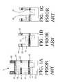
- FIGS. 1A-Cshow an illustrative conventional method for removing a crosslinked polymer.
- a structure 8includes, for example, a metal 10 in a substrate 12 , hardmask 14 , cap layer 16 , an ultra low dielectric constant (ULK) dielectric 18 , a hydrogenated silicon oxycarbide (SICOH) hardmask layer 20 and a hard mask 22 (e.g., tetraethyl orthosilicate Si(OC 2 H 5 ) 4 (TEOS)).
- Hard mask 22would be used as a sacrificial process-assist layer for via reactive ion etch (RIE) and strip.
- RIEreactive ion etch
- a first aspect of the inventionis directed to a method of forming an integrated circuit, the method comprising the steps of: forming an opening in a dielectric; at least partially filling the opening with an at most lightly crosslinked polymer; forming a crosslinked polymer over the at most lightly crosslinked polymer; performing other processing; removing the crosslinked polymer; and removing the at most lightly crosslinked polymer.
- the ULK dielectricmay include any now known or later developed dielectric having a dielectric constant lower than 3.9, i.e., the dielectric constant of silicon dioxide (SiO 2 ).
- Structure 108may further include a hydrogenated silicon oxycarbide (SICOH) hardmask layer 120 and a sacrificial hard mask 122 (e.g., tetraethyl orthosilicate Si(OC 2 H 5 ) 4 (TEOS)).
- SICOHhydrogenated silicon oxycarbide
- TEOStetraethyl orthosilicate Si(OC 2 H 5 ) 4
- this steppreferably includes performing a wet etch.
- the wet etchmay use at least one of: gamma butyl lactone (GBL) and tetra methyl ammonium hydroxide (TMAH).
- GBLgamma butyl lactone
- TMAHtetra methyl ammonium hydroxide
- Other strong organic solvents (such as GBL) or weak bases (such as TMAH)may be used also.
- this stepmay include performing a thermal decomposition at an appropriate temperature (e.g., 400° C. for PMMA-VBCB) to dissolve the particular polymer 162 , i.e., when polymer 162 includes either an un-crosslinked polymer or a lightly crosslinked polymer.
Landscapes
- Engineering & Computer Science (AREA)
- Physics & Mathematics (AREA)
- Condensed Matter Physics & Semiconductors (AREA)
- General Physics & Mathematics (AREA)
- Manufacturing & Machinery (AREA)
- Computer Hardware Design (AREA)
- Microelectronics & Electronic Packaging (AREA)
- Power Engineering (AREA)
- Chemical & Material Sciences (AREA)
- Chemical Kinetics & Catalysis (AREA)
- General Chemical & Material Sciences (AREA)
- Internal Circuitry In Semiconductor Integrated Circuit Devices (AREA)
Abstract
Description
Claims (20)
Priority Applications (1)
| Application Number | Priority Date | Filing Date | Title |
|---|---|---|---|
| US11/164,290US7253100B2 (en) | 2005-11-17 | 2005-11-17 | Reducing damage to ulk dielectric during cross-linked polymer removal |
Applications Claiming Priority (1)
| Application Number | Priority Date | Filing Date | Title |
|---|---|---|---|
| US11/164,290US7253100B2 (en) | 2005-11-17 | 2005-11-17 | Reducing damage to ulk dielectric during cross-linked polymer removal |
Publications (2)
| Publication Number | Publication Date |
|---|---|
| US20070111466A1 US20070111466A1 (en) | 2007-05-17 |
| US7253100B2true US7253100B2 (en) | 2007-08-07 |
Family
ID=38041457
Family Applications (1)
| Application Number | Title | Priority Date | Filing Date |
|---|---|---|---|
| US11/164,290Expired - Fee RelatedUS7253100B2 (en) | 2005-11-17 | 2005-11-17 | Reducing damage to ulk dielectric during cross-linked polymer removal |
Country Status (1)
| Country | Link |
|---|---|
| US (1) | US7253100B2 (en) |
Cited By (3)
| Publication number | Priority date | Publication date | Assignee | Title |
|---|---|---|---|---|
| US20080038934A1 (en)* | 2006-04-18 | 2008-02-14 | Air Products And Chemicals, Inc. | Materials and methods of forming controlled void |
| US8222136B2 (en)* | 2010-10-18 | 2012-07-17 | Taiwan Semiconductor Manufacturing Company, Ltd. | Method of forming contacts for a semiconductor device |
| US8420947B2 (en) | 2010-12-30 | 2013-04-16 | Globalfoundries Singapore Pte. Ltd. | Integrated circuit system with ultra-low k dielectric and method of manufacture thereof |
Citations (16)
| Publication number | Priority date | Publication date | Assignee | Title |
|---|---|---|---|---|
| US5585673A (en) | 1992-02-26 | 1996-12-17 | International Business Machines Corporation | Refractory metal capped low resistivity metal conductor lines and vias |
| US5695810A (en) | 1996-11-20 | 1997-12-09 | Cornell Research Foundation, Inc. | Use of cobalt tungsten phosphide as a barrier material for copper metallization |
| US6140226A (en) | 1998-01-16 | 2000-10-31 | International Business Machines Corporation | Dual damascene processing for semiconductor chip interconnects |
| US6303505B1 (en) | 1998-07-09 | 2001-10-16 | Advanced Micro Devices, Inc. | Copper interconnect with improved electromigration resistance |
| US6319819B1 (en) | 2000-01-18 | 2001-11-20 | Advanced Micro Devices, Inc. | Process for passivating top interface of damascene-type Cu interconnect lines |
| US6329118B1 (en) | 1999-06-21 | 2001-12-11 | Intel Corporation | Method for patterning dual damascene interconnects using a sacrificial light absorbing material |
| US6342733B1 (en) | 1999-07-27 | 2002-01-29 | International Business Machines Corporation | Reduced electromigration and stressed induced migration of Cu wires by surface coating |
| US6383925B1 (en) | 2000-02-04 | 2002-05-07 | Advanced Micro Devices, Inc. | Method of improving adhesion of capping layers to cooper interconnects |
| US6429128B1 (en) | 2001-07-12 | 2002-08-06 | Advanced Micro Devices, Inc. | Method of forming nitride capped Cu lines with reduced electromigration along the Cu/nitride interface |
| US6506677B1 (en) | 2001-05-02 | 2003-01-14 | Advanced Micro Devices, Inc. | Method of forming capped copper interconnects with reduced hillock formation and improved electromigration resistance |
| US20030134499A1 (en) | 2002-01-15 | 2003-07-17 | International Business Machines Corporation | Bilayer HDP CVD / PE CVD cap in advanced BEOL interconnect structures and method thereof |
| US6764951B1 (en) | 2002-02-28 | 2004-07-20 | Advanced Micro Devices, Inc. | Method for forming nitride capped Cu lines with reduced hillock formation |
| US20040152278A1 (en)* | 2000-02-14 | 2004-08-05 | Micron Technology, Inc. | Low dielectric constant STI with SOI devices |
| US6797652B1 (en) | 2002-03-15 | 2004-09-28 | Advanced Micro Devices, Inc. | Copper damascene with low-k capping layer and improved electromigration reliability |
| US6818557B1 (en) | 2002-12-12 | 2004-11-16 | Advanced Micro Devices, Inc. | Method of forming SiC capped copper interconnects with reduced hillock formation and improved electromigration resistance |
| US20040266201A1 (en) | 2003-06-24 | 2004-12-30 | International Business Machines Corporation | Method for forming damascene structure utilizing planarizing material coupled with diffusion barrier material |
- 2005
- 2005-11-17USUS11/164,290patent/US7253100B2/ennot_activeExpired - Fee Related
Patent Citations (18)
| Publication number | Priority date | Publication date | Assignee | Title |
|---|---|---|---|---|
| US5585673A (en) | 1992-02-26 | 1996-12-17 | International Business Machines Corporation | Refractory metal capped low resistivity metal conductor lines and vias |
| US6323554B1 (en) | 1992-02-26 | 2001-11-27 | International Business Machines Corporation | Refractory metal capped low resistivity metal conductor lines and vias formed using PVD and CVD |
| US5695810A (en) | 1996-11-20 | 1997-12-09 | Cornell Research Foundation, Inc. | Use of cobalt tungsten phosphide as a barrier material for copper metallization |
| US6140226A (en) | 1998-01-16 | 2000-10-31 | International Business Machines Corporation | Dual damascene processing for semiconductor chip interconnects |
| US6303505B1 (en) | 1998-07-09 | 2001-10-16 | Advanced Micro Devices, Inc. | Copper interconnect with improved electromigration resistance |
| US6365529B1 (en) | 1999-06-21 | 2002-04-02 | Intel Corporation | Method for patterning dual damascene interconnects using a sacrificial light absorbing material |
| US6329118B1 (en) | 1999-06-21 | 2001-12-11 | Intel Corporation | Method for patterning dual damascene interconnects using a sacrificial light absorbing material |
| US6342733B1 (en) | 1999-07-27 | 2002-01-29 | International Business Machines Corporation | Reduced electromigration and stressed induced migration of Cu wires by surface coating |
| US6319819B1 (en) | 2000-01-18 | 2001-11-20 | Advanced Micro Devices, Inc. | Process for passivating top interface of damascene-type Cu interconnect lines |
| US6383925B1 (en) | 2000-02-04 | 2002-05-07 | Advanced Micro Devices, Inc. | Method of improving adhesion of capping layers to cooper interconnects |
| US20040152278A1 (en)* | 2000-02-14 | 2004-08-05 | Micron Technology, Inc. | Low dielectric constant STI with SOI devices |
| US6506677B1 (en) | 2001-05-02 | 2003-01-14 | Advanced Micro Devices, Inc. | Method of forming capped copper interconnects with reduced hillock formation and improved electromigration resistance |
| US6429128B1 (en) | 2001-07-12 | 2002-08-06 | Advanced Micro Devices, Inc. | Method of forming nitride capped Cu lines with reduced electromigration along the Cu/nitride interface |
| US20030134499A1 (en) | 2002-01-15 | 2003-07-17 | International Business Machines Corporation | Bilayer HDP CVD / PE CVD cap in advanced BEOL interconnect structures and method thereof |
| US6764951B1 (en) | 2002-02-28 | 2004-07-20 | Advanced Micro Devices, Inc. | Method for forming nitride capped Cu lines with reduced hillock formation |
| US6797652B1 (en) | 2002-03-15 | 2004-09-28 | Advanced Micro Devices, Inc. | Copper damascene with low-k capping layer and improved electromigration reliability |
| US6818557B1 (en) | 2002-12-12 | 2004-11-16 | Advanced Micro Devices, Inc. | Method of forming SiC capped copper interconnects with reduced hillock formation and improved electromigration resistance |
| US20040266201A1 (en) | 2003-06-24 | 2004-12-30 | International Business Machines Corporation | Method for forming damascene structure utilizing planarizing material coupled with diffusion barrier material |
Non-Patent Citations (2)
| Title |
|---|
| Goldblatt, R.D. et al., "A High Performance 0.13 mum Copper BEOL Technology with Low-k Dielectric," Proceedings of the IEEE 2000 International Interconnect Technology Conference, pp. 261-263, 2000. |
| Hussein, M. et al., "A Novel Approach to Dual Damascene Patterning," Intel Corporation, Portland Technology Development. 3 pages, 2002. |
Cited By (5)
| Publication number | Priority date | Publication date | Assignee | Title |
|---|---|---|---|---|
| US20080038934A1 (en)* | 2006-04-18 | 2008-02-14 | Air Products And Chemicals, Inc. | Materials and methods of forming controlled void |
| US8399349B2 (en)* | 2006-04-18 | 2013-03-19 | Air Products And Chemicals, Inc. | Materials and methods of forming controlled void |
| US8846522B2 (en) | 2006-04-18 | 2014-09-30 | Air Products And Chemicals, Inc. | Materials and methods of forming controlled void |
| US8222136B2 (en)* | 2010-10-18 | 2012-07-17 | Taiwan Semiconductor Manufacturing Company, Ltd. | Method of forming contacts for a semiconductor device |
| US8420947B2 (en) | 2010-12-30 | 2013-04-16 | Globalfoundries Singapore Pte. Ltd. | Integrated circuit system with ultra-low k dielectric and method of manufacture thereof |
Also Published As
| Publication number | Publication date |
|---|---|
| US20070111466A1 (en) | 2007-05-17 |
Similar Documents
| Publication | Publication Date | Title |
|---|---|---|
| US6168726B1 (en) | Etching an oxidized organo-silane film | |
| US6913994B2 (en) | Method to form Cu/OSG dual damascene structure for high performance and reliable interconnects | |
| US6465358B1 (en) | Post etch clean sequence for making a semiconductor device | |
| US7125793B2 (en) | Method for forming an opening for an interconnect structure in a dielectric layer having a photosensitive material | |
| US6007733A (en) | Hard masking method for forming oxygen containing plasma etchable layer | |
| US6448185B1 (en) | Method for making a semiconductor device that has a dual damascene interconnect | |
| US20010055725A1 (en) | Method for patterning dual damascene interconnects using a sacrificial light absorbing material | |
| US7122484B2 (en) | Process for removing organic materials during formation of a metal interconnect | |
| US7439171B2 (en) | Method for manufacturing electronic device | |
| US20070134917A1 (en) | Partial-via-first dual-damascene process with tri-layer resist approach | |
| US20060163730A1 (en) | Electronic device and its manufacturing method | |
| US20040219796A1 (en) | Plasma etching process | |
| US6376384B1 (en) | Multiple etch contact etching method incorporating post contact etch etching | |
| KR20080060376A (en) | Manufacturing method of semiconductor device | |
| US20120100717A1 (en) | Trench lithography process | |
| US7687381B2 (en) | Method of forming electrical interconnects within insulating layers that form consecutive sidewalls including forming a reaction layer on the inner sidewall | |
| US7915115B2 (en) | Method for forming dual high-k metal gate using photoresist mask and structures thereof | |
| CN102201365A (en) | Method for producing semiconductor device | |
| US11081350B2 (en) | Semiconductor device and method of manufacture | |
| US6660652B2 (en) | Method for fabricating semiconductor device | |
| US7632689B2 (en) | Methods for controlling the profile of a trench of a semiconductor structure | |
| US7253100B2 (en) | Reducing damage to ulk dielectric during cross-linked polymer removal | |
| US10867803B2 (en) | Semiconductor device and method | |
| US20040048203A1 (en) | Method of manufacturing a semiconductor device for high speed operation and low power consumption | |
| US6861348B2 (en) | Pre-pattern surface modification of low-k dielectrics |
Legal Events
| Date | Code | Title | Description |
|---|---|---|---|
| AS | Assignment | Owner name:INTERNATIONAL BUSINESS MACHINES CORPORATION, NEW Y Free format text:ASSIGNMENT OF ASSIGNORS INTEREST;ASSIGNORS:DELLAGUARDIA, RONALD A.;EDELSTEIN, DANIEL C.;HICHRI, HABIB;AND OTHERS;REEL/FRAME:016792/0510;SIGNING DATES FROM 20051003 TO 20051013 Owner name:INTERNATIONAL BUSINESS MACHINES CORPORATION,NEW YO Free format text:ASSIGNMENT OF ASSIGNORS INTEREST;ASSIGNORS:DELLAGUARDIA, RONALD A.;EDELSTEIN, DANIEL C.;HICHRI, HABIB;AND OTHERS;SIGNING DATES FROM 20051003 TO 20051013;REEL/FRAME:016792/0510 | |
| FEPP | Fee payment procedure | Free format text:PAYOR NUMBER ASSIGNED (ORIGINAL EVENT CODE: ASPN); ENTITY STATUS OF PATENT OWNER: LARGE ENTITY | |
| STCF | Information on status: patent grant | Free format text:PATENTED CASE | |
| REMI | Maintenance fee reminder mailed | ||
| FPAY | Fee payment | Year of fee payment:4 | |
| SULP | Surcharge for late payment | ||
| AS | Assignment | Owner name:GOOGLE INC., CALIFORNIA Free format text:ASSIGNMENT OF ASSIGNORS INTEREST;ASSIGNOR:INTERNATIONAL BUSINESS MACHINES CORPORATION;REEL/FRAME:026664/0866 Effective date:20110503 | |
| FPAY | Fee payment | Year of fee payment:8 | |
| AS | Assignment | Owner name:GOOGLE LLC, CALIFORNIA Free format text:CHANGE OF NAME;ASSIGNOR:GOOGLE INC.;REEL/FRAME:044127/0735 Effective date:20170929 | |
| FEPP | Fee payment procedure | Free format text:MAINTENANCE FEE REMINDER MAILED (ORIGINAL EVENT CODE: REM.); ENTITY STATUS OF PATENT OWNER: LARGE ENTITY | |
| LAPS | Lapse for failure to pay maintenance fees | Free format text:PATENT EXPIRED FOR FAILURE TO PAY MAINTENANCE FEES (ORIGINAL EVENT CODE: EXP.); ENTITY STATUS OF PATENT OWNER: LARGE ENTITY | |
| STCH | Information on status: patent discontinuation | Free format text:PATENT EXPIRED DUE TO NONPAYMENT OF MAINTENANCE FEES UNDER 37 CFR 1.362 | |
| FP | Lapsed due to failure to pay maintenance fee | Effective date:20190807 |