US7253076B1 - Methods for forming and integrated circuit structures containing ruthenium and tungsten containing layers - Google Patents
Methods for forming and integrated circuit structures containing ruthenium and tungsten containing layersDownload PDFInfo
- Publication number
- US7253076B1 US7253076B1US09/590,795US59079500AUS7253076B1US 7253076 B1US7253076 B1US 7253076B1US 59079500 AUS59079500 AUS 59079500AUS 7253076 B1US7253076 B1US 7253076B1
- Authority
- US
- United States
- Prior art keywords
- layer
- ruthenium
- forming
- ruthenium oxide
- electrically conductive
- Prior art date
- Legal status (The legal status is an assumption and is not a legal conclusion. Google has not performed a legal analysis and makes no representation as to the accuracy of the status listed.)
- Expired - Fee Related, expires
Links
Images


Classifications
- H—ELECTRICITY
- H10—SEMICONDUCTOR DEVICES; ELECTRIC SOLID-STATE DEVICES NOT OTHERWISE PROVIDED FOR
- H10B—ELECTRONIC MEMORY DEVICES
- H10B12/00—Dynamic random access memory [DRAM] devices
- H—ELECTRICITY
- H10—SEMICONDUCTOR DEVICES; ELECTRIC SOLID-STATE DEVICES NOT OTHERWISE PROVIDED FOR
- H10D—INORGANIC ELECTRIC SEMICONDUCTOR DEVICES
- H10D1/00—Resistors, capacitors or inductors
- H10D1/60—Capacitors
- H10D1/68—Capacitors having no potential barriers
- H10D1/692—Electrodes
- H10D1/711—Electrodes having non-planar surfaces, e.g. formed by texturisation
- H10D1/712—Electrodes having non-planar surfaces, e.g. formed by texturisation being rough surfaces, e.g. using hemispherical grains
- H—ELECTRICITY
- H10—SEMICONDUCTOR DEVICES; ELECTRIC SOLID-STATE DEVICES NOT OTHERWISE PROVIDED FOR
- H10D—INORGANIC ELECTRIC SEMICONDUCTOR DEVICES
- H10D1/00—Resistors, capacitors or inductors
- H10D1/60—Capacitors
- H10D1/68—Capacitors having no potential barriers
- H10D1/692—Electrodes
- H10D1/694—Electrodes comprising noble metals or noble metal oxides
- H—ELECTRICITY
- H01—ELECTRIC ELEMENTS
- H01L—SEMICONDUCTOR DEVICES NOT COVERED BY CLASS H10
- H01L21/00—Processes or apparatus adapted for the manufacture or treatment of semiconductor or solid state devices or of parts thereof
- H01L21/02—Manufacture or treatment of semiconductor devices or of parts thereof
- H01L21/02104—Forming layers
- H01L21/02107—Forming insulating materials on a substrate
- H01L21/02109—Forming insulating materials on a substrate characterised by the type of layer, e.g. type of material, porous/non-porous, pre-cursors, mixtures or laminates
- H01L21/02112—Forming insulating materials on a substrate characterised by the type of layer, e.g. type of material, porous/non-porous, pre-cursors, mixtures or laminates characterised by the material of the layer
- H01L21/02172—Forming insulating materials on a substrate characterised by the type of layer, e.g. type of material, porous/non-porous, pre-cursors, mixtures or laminates characterised by the material of the layer the material containing at least one metal element, e.g. metal oxides, metal nitrides, metal oxynitrides or metal carbides
- H01L21/02175—Forming insulating materials on a substrate characterised by the type of layer, e.g. type of material, porous/non-porous, pre-cursors, mixtures or laminates characterised by the material of the layer the material containing at least one metal element, e.g. metal oxides, metal nitrides, metal oxynitrides or metal carbides characterised by the metal
- H01L21/02183—Forming insulating materials on a substrate characterised by the type of layer, e.g. type of material, porous/non-porous, pre-cursors, mixtures or laminates characterised by the material of the layer the material containing at least one metal element, e.g. metal oxides, metal nitrides, metal oxynitrides or metal carbides characterised by the metal the material containing tantalum, e.g. Ta2O5
- H—ELECTRICITY
- H01—ELECTRIC ELEMENTS
- H01L—SEMICONDUCTOR DEVICES NOT COVERED BY CLASS H10
- H01L21/00—Processes or apparatus adapted for the manufacture or treatment of semiconductor or solid state devices or of parts thereof
- H01L21/02—Manufacture or treatment of semiconductor devices or of parts thereof
- H01L21/02104—Forming layers
- H01L21/02107—Forming insulating materials on a substrate
- H01L21/02109—Forming insulating materials on a substrate characterised by the type of layer, e.g. type of material, porous/non-porous, pre-cursors, mixtures or laminates
- H01L21/02112—Forming insulating materials on a substrate characterised by the type of layer, e.g. type of material, porous/non-porous, pre-cursors, mixtures or laminates characterised by the material of the layer
- H01L21/02172—Forming insulating materials on a substrate characterised by the type of layer, e.g. type of material, porous/non-porous, pre-cursors, mixtures or laminates characterised by the material of the layer the material containing at least one metal element, e.g. metal oxides, metal nitrides, metal oxynitrides or metal carbides
- H01L21/02197—Forming insulating materials on a substrate characterised by the type of layer, e.g. type of material, porous/non-porous, pre-cursors, mixtures or laminates characterised by the material of the layer the material containing at least one metal element, e.g. metal oxides, metal nitrides, metal oxynitrides or metal carbides the material having a perovskite structure, e.g. BaTiO3
- H—ELECTRICITY
- H10—SEMICONDUCTOR DEVICES; ELECTRIC SOLID-STATE DEVICES NOT OTHERWISE PROVIDED FOR
- H10D—INORGANIC ELECTRIC SEMICONDUCTOR DEVICES
- H10D1/00—Resistors, capacitors or inductors
- H10D1/60—Capacitors
- H10D1/68—Capacitors having no potential barriers
- H10D1/682—Capacitors having no potential barriers having dielectrics comprising perovskite structures
Definitions
- the inventionpertains to semiconductor devices and the fabrication thereof, and particularly to ruthenium- and tungsten-containing electrically conductive layers and the formation and use thereof.
- a capacitorgenerally includes two electrical conductors in close proximity to, but separated from, each other.
- the two conductorsform the “plates” of the capacitor, and may be separated by a dielectric material.
- the fabrication of integrated circuitsinvolves the formation of electrically conductive layers for use as various circuit components, including for use as capacitor plates.
- Memory circuitssuch as DRAMs and the like, use electrically conductive layers to form the opposing plates of storage cell capacitors.
- Various stepsmay be taken to increase or preserve capacitance without increasing the occupied area.
- material(s) having higher dielectric constantmay be used between the capacitor plates.
- the plate surfacesmay be roughened to increase the effective surface area of the plates without increasing the area occupied by he capacitor.
- One method for providing a roughened surface for a plate of a storage cell capacitoris to form the plate of hemispherical grain polysilicon (HSG), possibly with an overlying metal layer.
- HSGhemispherical grain polysilicon
- the hemispherical grains of HSGenhance the surface area of the plate without increasing its occupied area.
- HSGpresents difficulties in fabrication, however, because of the formation of silicon dioxide on and near the HSG.
- a silicon dioxide layermay form on the HSG, particularly during deposition of the capacitor's dielectric layer. Even with an intervening metal layer present, oxygen from the deposition of the dielectric layer can diffuse through the metal layer, forming silicon dioxide at the polysilicon surface. Silicon diffusion through the metal layer may also produce a silicon dioxide layer between the metal and the dielectric layers.
- Silicon dioxide between the metal layer and the HSGcan degrade the electrical contact to the metal capacitor plate surface. Silicon dioxide between the metal layer and the dielectric layer can decrease the capacitance of the resulting capacitor.
- a diffusion barrier layermay be employed between the HSG and the metal layer.
- the greater the total number of layersthe larger the required minimum area occupied by the capacitor.
- the upper surface of each additional layer depositedtends to be smoother than the underlying surface, reducing the increased surface area provided by an underlying rough layer.
- the present inventionprovides improved conductive layers, dielectric layers, capacitors, methods for forming such layers, and capacitors using the layers.
- enhanced-surface-area (rough-surfaced) ruthenium containing electrically conductive layersare provided. These layers are compatible with high-dielectric-constant materials and are useful in the formation of integrated circuits, particularly for plates of storage capacitors in memory cells.
- the enhanced-surface-area electrically conductive layermay be formed by first forming a ruthenium oxide containing film or layer.
- the layermay be stoichiometric or non-stoichiometric, and may be amorphous or may have both ruthenium (Ru) and ruthenium oxide (RuO 2 ) phases and may include other materials.
- the filmmay be formed, for example, by chemical vapor deposition techniques or by sputtering or any suitable techniques.
- the filmmay be formed over an underlying layer which may be electrically conductive.
- the ruthenium oxide filmmay be processed at low pressure and high temperature—generally at pressures at least about 75 torr or below, desirably about 20 torr or below, most desirably about 5 torr or below—and at temperatures in the range of about 500 to 900° C., desirably about 750 to about 850° C.—so as to convert at least some of the ruthenium oxide to ruthenium and to yield a roughened ruthenium-containing layer with a mean grain size desirably in the range of about 100 Angstroms or larger.
- the heating process, or annealis desirably performed in a non-oxidizing ambient.
- a nitrogen-supplying ambient or nitrogen-supplying reducing ambientmay be used during the anneal.
- a nitrogen-supplying reducing ambientmay be used to passivate the ruthenium for improved compatibility with high-dielectric-constant dielectric materials.
- a nitrogen-supplying reducing ambientmay be used in a post-anneal to passivate an already roughened layer.
- a post-anneal in an oxidizing ambientmay be performed, following either the roughening anneal or the nitride-passivation anneal, as desired. This oxidizing post-anneal provides oxygen to the roughened layer to reduce the tendency of the ruthenium to scavenge oxygen during later processing.
- the enhanced-surface-area layermay be formed with or without a pre-anneal, performed at a higher pressure (such as about 600 torr), before the low pressure, high temperature anneal.
- the roughened layer of rutheniummay be used to provide an enhanced-surface-area electrically conductive layer.
- the roughened layer of rutheniummay be formed on an underlying electrically conductive layer, with the roughened layer and the underlying layer together functioning as an enhanced-surface-area electrically conductive layer.
- an electrically conductive layermay be formed on or over the roughened layer, with the overlying electrically conductive layer and the roughened layer constituting an enhanced-surface area electrically conductive layer.
- the resulting enhanced-surface-area electrically conductive layermay be used to form a plate of a storage capacitor in an integrated circuit, such as in a memory cell of a DRAM or the like.
- the ruthenium-containing enhanced-surface-area electrically conductive layerparticularly in the case of an anneal in nitrogen-supplying reducing ambient with an oxidizing post-anneal, has reduced tendency toward oxidation and is thus more compatible with the use of high-dielectric-constant dielectric materials, while still providing enhanced surface area.
- the ruthenium-containing layeroxidizes, it remains conductive.
- An additional metal layerthus may potentially be omitted from the capacitor structure, allowing smaller dimensions for capacitors with the same or even greater capacitance.
- a tungsten nitride layeris provided as a first electrode layer.
- a dielectric layer and a second electrode layerare conformally applied to the first electrode layer to form a capacitor.
- the capacitor, or at least the tungsten nitride layeris annealed at an anneal temperature to increase the capacitance of the capacitor.
- the anneal temperatureis at least 500 C and the capacitor (or the tungsten nitride layer) is maintained at the anneal temperature for at least 30 seconds.
- FIG. 1is a partial cross-section of layers used in a process according to one embodiment, the layers including a ruthenium oxide containing layer.
- FIG. 2is a cross-section of the layers of FIG. 1 after a low-pressure, high-temperature anneal, including a roughened layer.
- FIG. 3is a partial plan view of the layers of FIG. 2
- FIG. 4is a cross-section similar to that of FIG. 2 but having an additional layer underlying the roughened layer.
- FIG. 5is a cross section of the layers of FIG. 2 after formation of an additional layer overlying the roughened layer.
- FIG. 6is a cross section of an enhanced-surface-area electrically conductive layer with a dielectric layer formed thereon according to one embodiment.
- FIG. 7is a cross section of the layers of FIG. 6 with an electrically conductive layer formed on the dielectric layer.
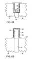
- FIGS. 8A–8Bare cross-sections of two embodiments of capacitor structures that include a roughened layer.
- FIGS. 9A–9Care cross-sections of capacitor structures that include a tungsten nitride electrode layer.
- the present inventionallows creation of a surface-area-enhanced ruthenium electrically conductive layer that has improved compatibility with high-dielectric-constant (“high- ⁇ ”) dielectric materials as compared to hemispherical-grain polysilicon (HSG).
- the surface-area-enhanced electrically conductive layeris created by heating a film or layer comprising ruthenium oxide such as the layer 12 of FIG. 1 .
- the heating processwhich may anneal the film or layer, is typically performed at low pressures of less than about 75 torr, desirably less than about 20 torr, and most desirably less than about 5 torr, and at high temperatures in the range of about 500 to 900° C., desirably about 750 to 850° C.
- the treatmentis desirably performed in a non-oxidizing ambient.
- the heating processmay be performed in a noble ambient, nitrogen ambient, or the like, or in a reducing ambient, which may reduce the temperature required.
- the heating processmay also be performed in an electrically neutral environment, or with plasma or glow-discharge assistance or the like, which may also reduce the temperature required. Heating under relatively low pressure converts at least a portion of the ruthenium oxide to ruthenium and produces a rough surface on the layer. Temperature and pressure are preferably selected so as to enhance the ruthenium oxide to ruthenium conversion.
- the surface-area-enhanced electrically conductive layermay be formed on a supporting structure 10 shown in partial cross-section in FIG. 1 .
- the supporting structure 10may be any structure present in or on an integrated circuit during the fabrication thereof.
- the supporting structuremay be an electrically conductive material that will be in electrical contact with a capacitor plate formed by the surface-area-enhanced electrically conductive layer.
- the ruthenium oxide layer 12may be formed by any suitable method. Specific examples of such methods include chemical vapor deposition (CVD) or related process, or sputtering or related process, or the like.
- the ruthenium oxide layermay be stoichiometric ruthenium oxide (RuO 2 ) or non-stoichiometric ruthenium oxide (RuO x ).
- the depositionmay be performed, for example, at pressures of 1–20 torr, desirably about 5 torr.
- the oxygenmay be supplied in the form of O 2 or other oxidizing gas, such as N 2 O, NO, or ozone (O 3 ).
- the oxygenating gas and a ruthenium precursor, and suitable diluent gasses, if desired,may be supplied at suitable flow rates, such as in the range of about 100–2000 sccm.
- the ruthenium precursorcan be delivered by direct vaporization.
- Depositionmay be performed for a time in the range of about 10 to 500 seconds, desirably for sufficient time and under sufficient conditions to deposit RuO x or RuO 2 to a thickness in the range of about 100 to 600 Angstroms.
- the resulting ruthenium oxide layer 12may optionally be pre-annealed, such as by rapid thermal anneal (RTA) in hydrogen or other suitable anneal environment at pressures in the range of 500 to 700 torr and temperatures in the range of 500 to 900° C.
- RTArapid thermal anneal
- the pre-annealstabilizes the film, promoting crystallization of ruthenium and ruthenium oxide phases.
- the ruthenium oxide layer 12is then treated at low pressure and high temperature as described above.
- the treatmentmay reduce the proportion of ruthenium oxide in the layer and increase the proportion of ruthenium.
- the ruthenium oxide in the ruthenium oxide layer 12is partially or completely converted to ruthenium by the anneal, leaving an enhanced-surface-area layer 16 shown in the cross section of FIG. 2 . While the enhanced-surface-area layer 16 is referred to by separate reference character for convenience herein, it should be noted that the layer 16 is formed from the layer 12 , and is the same layer in that sense.
- FIG. 3shows a partial plan view of the roughened ruthenium layer 16 of FIG. 2 .
- example roughened ruthenium layer 16 shown in the figuresis discontinuous, this is by way of example only and continuous films may also be produced. Increased thickness of the initial layer 12 tends to produce more continuous films, as does reduced temperature and increased pressure during the anneal and reduced anneal time.
- the annealmay be performed in a noble, nitrogen, or reducing ambient or the like.
- an annealmay be performed in a nitrogen-supplying reducing ambient such as such as ammonia, nitrogen, a nitrogen and hydrogen mixture, and the like.
- the anneal parametersmay be selected such that “nitrogen-passivated” ruthenium in the form of RuN x is formed in the layer 16 , at least near the outermost surfaces thereof, passivating the layer 16 .
- nitride passivationmay be used in the form of a post-anneal in a nitrogen-supplying reducing ambient.
- a desirably brief post-anneal in an oxidizing ambient such as oxygen or ozonemay be performed on the already roughened layer 16 , to form “oxygen-passivated” ruthenium or ruthenium nitride in the outermost portions of the layer 16 (RuO x N y or RuO x ), in order to reduce or prevent the ruthenium from later scavenging oxygen from a nearby dielectric material.
- the oxidizing post-annealmay optionally follow a nitride passivation post-anneal.
- the roughened ruthenium layer 16together with the supporting structure 10 if electrically conductive, may together constitute an enhanced-surface-area electrically conductive layer 26 compatible with high-dielectric-constant dielectric materials.
- the layer 16 produced such as described abovemay also be used in cooperation with other layers. This may be useful in cases where the supporting structure 10 may not be electrically conductive or may be incompatible with high-dielectric-constant dielectric materials.
- “on” used with respect to two layers, one “on” the other,means at least some contact between the layers, while “over” means the layers are in close proximity, but possibly with one or more additional intervening layers such that contact is not required. Neither “on” nor “over” implies any directionality as used herein.
- a layer 22 of materialmay be formed over the supporting structure 10 , with the roughened ruthenium layer 16 then formed on the layer 22 .
- the layer 22may be an electrically conductive layer to electrically connect all portions of layer 16 .
- the layer 22may also act as a barrier layer to prevent contact between high-dielectric-constant dielectrics, to be used for capacitor formation, and the supporting structure 10 . If the layer 22 is an electrically conductive layer, layer 22 together with layer 16 constitute an enhanced-surface-area electrically conductive layer 26 .
- Any compatible electrically conductive materialmay be used, such as Pt, Ir, IrO x , Rh, RuSi x , and SrRuO x and alloys thereof as well as RuSiO x and RuSiN x , for example.
- a layer 24 of electrically conductive materialmay be formed conformally over the layer 16 and over the supporting structure 10 .
- the layer 24together with the layer 16 , then constitutes an enhanced-surface-area electrically conductive layer 26 .
- the layer 24may function to electrically connect all portions of layer 16 , and may also function as a barrier layer to prevent contact between high-dielectric-constant dielectrics and the supporting structure 10 .
- Examples of such electrically conductive materialsinclude the materials listed in the preceding paragraph. Ruthenium oxide is a desirable material because of compatibility with the underlying ruthenium layer 16 .
- the supporting structure 10 and/or one or more layers above or below the layer 16may be electrically conductive and may be employed as needed to obtain conductivity and other desired properties.
- the resulting enhanced-surface-area electrically conductive layer 26shown by way of example in FIGS. 3 , 5 , and 6 , is represented generically as layer 26 in FIG. 6 .
- a layer 28 of dielectric materialmay be formed conformally over the enhanced-surface-area electrically conductive layer, as shown in FIG. 6 .
- a high-dielectric-constant dielectric materialgenerally any dielectric with a dielectric constant of at least 9
- tantalum pentoxideTa 2 O 5
- Other high-constant dielectricsmay also be employed, such as barium strontium titanium oxide (Ba,Sr)TiO 3 , lead zirconium titanium oxide Pb(Zr,Ti)O 3 , and strontium bismuth tantalum oxide (SrBi 2 Ta 2 O 9 ), for example.
- the layer 28is desirably sufficiently thin and conforming to provide an at least somewhat enhanced surface area on the surface away from the layer 26 .
- An electrically conductive layer 30may then be formed conformally over the dielectric layer 28 , as shown in FIG. 7 .
- the surface of layer 30 uppermost in the figureis not shown because the layer may generally be of any thickness sufficiently thick to insure continuity of the layer and sufficiently thin to fit within the overall volume allotted to the capacitor.
- the surface of layer 30 next to the dielectric layer 28desirably conforms to the enhanced surface area of the dielectric layer 28 , providing an enhanced surface area for the electrically conductive layer 30 as well.
- the two electrically conductive layers, layers 26 and 30form the two plates of a capacitor. Both plates desirably have enhanced surface area relative to the area occupied by the capacitor.
- the supporting structure 10may be an electrically conductive plug of polysilicon or other electrically conductive material formed at the bottom of an opening in a dielectric material 32 such as borophosphosilicate glass (BPSG).
- BPSGborophosphosilicate glass
- the lower end of the plugtypically electrically contacts a circuit element such as a transistor gate (not shown).
- the BPSGitself functions a supporting structure for the capacitor plate structure.
- the relative thinness of the capacitor structure provided by the layer structure of FIG. 7maximizes the capacitor plate surface area in the container capacitor of FIG. 8A , particularly for the inner (upper) electrode, the surface area of which decreases most rapidly with increasing thickness of the layer structure.
- the use of the enhanced-surface-area ruthenium electrically conductive layerthus provides improved capacitance in a given area.
- the supporting structure 10includes a plug 25 that extends from a surface 27 and the layers 26 , 28 , 30 are formed conformally on the plug 25 .
- ruthenium oxidewas deposited on substrates of BPSG to a thickness of about 600 Angstroms by CVD.
- the ruthenium oxide layerswere pre-annealed in nitrogen for one minute at 800° C. and 600 torr, then annealed at 800° C. in nitrogen for varying times and at varying pressures. Such a pre-anneal can be omitted.
- layers annealed for eight minutes at 4.5 torrshowed marked surface roughness with mean grain size of about 100 Angstroms or larger, with good uniformity over the substrate surface.
- Layers annealed for eight minutes at 60 torrshowed some surface roughness with a mean grain approaching 100 Angstroms, but with generally less roughness than at 4.5 torr.
- Layers annealed for eight minutes at 600 torrshowed generally still less roughness and still smaller grain sizes than at 60 torr.
- Layers annealed for two minutes at 4.5 torralso showed a marked surface roughness, with possibly slightly less uniformity over the substrate surface than those annealed for eight minutes.
- X-ray diffraction studies of the annealed layersshowed ruthenium as the primary constituent but the Ru/RuO 2 ratio varied with processing conditions.
- Superior capacitors including metal-insulator-metal (MIM) capacitorscan be obtained using a tungsten nitride layer as an electrode.
- the tungsten nitride layercan be formed by reactive sputtering of a tungsten target in a nitrogen containing ambient, or by a chemical vapor deposition process (CVD) such as a plasma enhanced CVD (PECVD), a metallo-organic CVD (MOCVD) process, atomic layer deposition (ALD), or other process.
- CVDchemical vapor deposition process
- PECVDplasma enhanced CVD
- MOCVDmetallo-organic CVD
- ALDatomic layer deposition
- the tungsten nitride layeris conveniently formed using a thermal CVD process using tungsten fluoride (WF 6 ) and ammonia (NH 3 ) as precursors, and a 300 Angstrom thick layer can be formed using such a process in about 1–3 minutes.
- the thickness of the tungsten nitride layercan be varied but typically the thickness is in the range of 100–1000 Angstroms.
- the tungsten nitride layercan contain a mixture of a stable tungsten nitride compound W 2 N and a metastable tungsten nitride compound WN.
- the metastable compound WNcan be converted to the stable tungsten nitride compound W 2 N in a rapid thermal process (RTP) in which the temperature of the tungsten nitride layer is rapidly raised to an anneal temperature in the range of 600–800 C and held at the anneal temperature for about 60 seconds.
- RTPrapid thermal process
- the temperature of the tungsten nitride layeris ramped up to and down from an anneal temperature of 700 C in less than about 30 seconds.
- Such an anneal processis typically performed before a dielectric layer and a second electrode are formed on the tungsten nitride layer so that a capacitor structure is otherwise complete.
- the metastable compound WNmay include defects and may be preferentially oxidized during deposition of dielectric materials such as Ta 2 O 5 and subsequent annealing processes. Therefore, the capacitance of a capacitor formed without an anneal process tends to be low. In addition, the presence of defects tends to increase leakage currents. In a completed capacitor, the anneal process tends to increase capacitance by about 20% with respect to a capacitor without annealing and to reduce leakage currents that occur when voltages are applied to the electrodes.
- a dielectric layer consisting of any of various dielectric materialsis formed on the tungsten nitride layer.
- Suitable dielectric materialsinclude high-dielectric-constant materials such as tantalum pentoxide (Ta 2 O 5 ), doped Ta 2 O 5 such as Ti-doped Ta 2 O 5 , barium strontium titanium oxide (Ba,Sr)TiO 3 , lead zirconium titanium oxide Pb(Zr,Ti)O 3 , strontium bismuth tantalum oxide (SrBi 2 Ta 2 O 9 ), BaTiO 3 , SrTiO 3 , Pb(Zr,Ti)O 3 , SrBi 2 Ta 2 O 9 , SrBi 2 Nb 2 O 9 , SrBi 2 (Nb,Ta) 2 O 9 , (Pb,La)(Zr,Ti)O 3 , Al 2 O 3 , ZrO 2 , HfO 2 , and SiO x N y
- Ta 2 O 5formation of a stoichiometric compound is preferred so that the Ta 2 O 5 layer is not a tantalum rich layer, because tantalum rich Ta 2 O 5 layers tend to be conducting, not insulating.
- Tantalum pentoxide dielectric layersare preferred in some applications because of its large dielectric constant and its stability.
- tantalum pentoxideis typically formed using a MOCVD process in an oxidizing ambient such as an oxygen, ozone, or N 2 O ambient. While many electrode layer materials cannot be exposed to oxidizing ambients, tungsten nitride is relatively unaffected by such ambients and therefore facilitates the use of tantalum pentoxide dielectric layers.
- An electrode layer of tungsten nitride or other conducting materialis formed on the dielectric layer and serves as a top electrode for the capacitor.
- Other suitable conducting materialsinclude TiN, TiON, WN x , TaN, Ta, Pt, Rh, Pt—Rh, Pt—RhO x , Ru, RuO x , Ir, IrO x , Pt—Ru, Pt—RuO x , Pt—Ir, Pt—IrO x , SrRuO 3 , Au, Pd, Al, Mo, Ag, polysilicon, and alloys thereof.
- These electrode materialscan be formed by various processes. For example, ruthenium and platinum/rhodium are conveniently formed using a CVD process. After the dielectric layer and the electrode layers are formed, the capacitor is annealed as described above.
- FIGS. 9A–9Cillustrate several example capacitor geometries that include tungsten nitride electrodes.
- a plate capacitor 51is formed on a surface of a substrate 53 .
- the substrate 53can be any of various substrate materials including GaAs, silicon, or BPSG.
- the capacitor 51includes a first electrode 55 , a second electrode 57 , and a dielectric layer 59 .
- the first electrode 55is a tungsten nitride layer
- the dielectric layer 58is a Ta 2 O 5 layer
- the second electrodeis a TiN layer
- the substrate 53is BPSG.
- Electrodes of a capacitorsuch as the capacitor 51
- some electrical currentflows between the electrodes. This current is generally undesirable and is referred to as a “leakage” current.
- Plate capacitors having electrodes of tungsten nitridehave leakage currents of as little as about 20 nA/cm 2 , or as low as about 5 nA/cm 2 for capacitors having dielectric layers 100 Angstroms thick and with an applied voltage of 1 V.
- a container capacitor 61is formed in an etched recess 62 in a substrate 63 .
- a tungsten nitride electrode layer 65covers a bottom surface 66 and a side surface 67 of the recess 62 .
- a Ta 2 O 5 dielectric layer 69covers the electrode layer 65 , substantially filling the recess 62 and a tungsten nitride electrode layer 71 (or other conductive layer) covers the dielectric layer 69 .
- the dimensions of the recess 62are selected to provide a desired capacitance, and can be selected in conjunction with a minimum feature size for other circuit elements that are formed on the substrate 63 .
- the recess 62has a diameter D of 200 nm and a depth Z of 1000 nm.
- the tungsten nitride layeris preferably about 300 Angstroms (30 nm) thick.
- Tungsten nitride layers thinner than about 100 Angstroms (10 nm)tend to have voids. Because of these voids, such layers do not act as continuous electrodes, reducing the capacitance of the capacitor 61 .
- Tungsten nitride layers thicker than about 1000 Angstroms (100 nm)tend to occupy too much of the volume of the recess 62 , also limiting the capacitance of the capacitor 61 .
- thicker tungsten nitride layerscan be used without sacrificing too much capacitance.
- the recess 62is generally formed in the substrate 63 with an etching process. If the substrate 63 is BPSG, the recess 62 can be formed with a dry etch process such as plasma etching. While other etching processes are possible, because the recess 62 is deeper than wide, a selected etch process is preferably anisotropic.
- a stud capacitor 71is formed on a plug 73 that extends from a surface 75 of a substrate 77 .
- a tungsten nitride electrode layer 79is formed on the plug 73 and is covered with a dielectric layer 81 and an electrode layer 83 .
- the dielectric layer 81 and the electrode layercan be formed of any of the materials mentioned above. Representative materials are Ta 2 O 5 and TiN for the dielectric layer 81 and the electrode layer 83 , respectively.
- the plug 73may be an electrically conductive plug of polysilicon or other electrically conductive material formed in a recess in the substrate 77 such as a borophosphosilicate glass (BPSG). The lower end of the plug typically electrically contacts a circuit element such as a transistor gate (not shown).
- BPSGborophosphosilicate glass
- a tungsten nitride layeris deposited directly on a substrate such as BPSG.
- a tungsten nitride layercan be formed or deposited on a titanium nitride (TiN) adhesion layer, or other adhesion layer, to improve the bonding of the tungsten nitride layer to the substrate.
- TiNtitanium nitride
- the enhanced-surface-area layerscan be used in ferroelectric memories to improve storage capacity.
- the scope of coverageis accordingly defined not by the particular example embodiments and variations explicitly described above, but by the claims below.
Landscapes
- Semiconductor Memories (AREA)
- Semiconductor Integrated Circuits (AREA)
Abstract
Description
Claims (26)
Priority Applications (12)
| Application Number | Priority Date | Filing Date | Title |
|---|---|---|---|
| US09/590,795US7253076B1 (en) | 2000-06-08 | 2000-06-08 | Methods for forming and integrated circuit structures containing ruthenium and tungsten containing layers |
| AU2001275398AAU2001275398A1 (en) | 2000-06-08 | 2001-06-07 | Methods for forming and integrated circuit structures containing ruthenium and tungsten containing layers |
| PCT/US2001/018585WO2001095378A2 (en) | 2000-06-08 | 2001-06-07 | Methods for forming and integrated circuit structures containing ruthenium and tungsten containing layers |
| JP2002502821AJP4216585B2 (en) | 2000-06-08 | 2001-06-07 | Method for forming a layer containing ruthenium and tungsten, and integrated circuit structure including these layers |
| CNB2006100925169ACN100446178C (en) | 2000-06-08 | 2001-06-07 | Formation method and integrated circuit structure comprising ruthenium and tungsten comprising layers |
| CNB018109195ACN1270352C (en) | 2000-06-08 | 2001-06-07 | Formation method and integrated circuit structure comprising ruthenium and tungsten comprising layers |
| EP01942105.6AEP1297562B1 (en) | 2000-06-08 | 2001-06-07 | Methods for forming and integrated circuit structures containing ruthenium containing layers |
| KR1020027016729AKR100746192B1 (en) | 2000-06-08 | 2001-06-07 | Integrated circuit structure comprising ruthenium and tungsten containing layer and method for forming the same |
| US10/002,779US6833576B2 (en) | 2000-06-08 | 2001-10-29 | Methods for forming and integrated circuit structures containing ruthenium and tungsten containing layers |
| US10/002,906US6596583B2 (en) | 2000-06-08 | 2001-10-29 | Methods for forming and integrated circuit structures containing ruthenium and tungsten containing layers |
| US10/226,008US20030003697A1 (en) | 2000-06-08 | 2002-08-21 | Methods for forming and integrated circuit structures containing ruthenium and tungsten containing layers |
| US11/235,866US20060076597A1 (en) | 2000-06-08 | 2005-09-26 | Methods for forming and integrated circuit structures containing ruthenium and tungsten containing layers |
Applications Claiming Priority (1)
| Application Number | Priority Date | Filing Date | Title |
|---|---|---|---|
| US09/590,795US7253076B1 (en) | 2000-06-08 | 2000-06-08 | Methods for forming and integrated circuit structures containing ruthenium and tungsten containing layers |
Related Child Applications (2)
| Application Number | Title | Priority Date | Filing Date |
|---|---|---|---|
| US10/002,906DivisionUS6596583B2 (en) | 2000-06-08 | 2001-10-29 | Methods for forming and integrated circuit structures containing ruthenium and tungsten containing layers |
| US10/002,779DivisionUS6833576B2 (en) | 2000-06-08 | 2001-10-29 | Methods for forming and integrated circuit structures containing ruthenium and tungsten containing layers |
Publications (1)
| Publication Number | Publication Date |
|---|---|
| US7253076B1true US7253076B1 (en) | 2007-08-07 |
Family
ID=24363746
Family Applications (5)
| Application Number | Title | Priority Date | Filing Date |
|---|---|---|---|
| US09/590,795Expired - Fee RelatedUS7253076B1 (en) | 2000-06-08 | 2000-06-08 | Methods for forming and integrated circuit structures containing ruthenium and tungsten containing layers |
| US10/002,779Expired - Fee RelatedUS6833576B2 (en) | 2000-06-08 | 2001-10-29 | Methods for forming and integrated circuit structures containing ruthenium and tungsten containing layers |
| US10/002,906Expired - LifetimeUS6596583B2 (en) | 2000-06-08 | 2001-10-29 | Methods for forming and integrated circuit structures containing ruthenium and tungsten containing layers |
| US10/226,008AbandonedUS20030003697A1 (en) | 2000-06-08 | 2002-08-21 | Methods for forming and integrated circuit structures containing ruthenium and tungsten containing layers |
| US11/235,866AbandonedUS20060076597A1 (en) | 2000-06-08 | 2005-09-26 | Methods for forming and integrated circuit structures containing ruthenium and tungsten containing layers |
Family Applications After (4)
| Application Number | Title | Priority Date | Filing Date |
|---|---|---|---|
| US10/002,779Expired - Fee RelatedUS6833576B2 (en) | 2000-06-08 | 2001-10-29 | Methods for forming and integrated circuit structures containing ruthenium and tungsten containing layers |
| US10/002,906Expired - LifetimeUS6596583B2 (en) | 2000-06-08 | 2001-10-29 | Methods for forming and integrated circuit structures containing ruthenium and tungsten containing layers |
| US10/226,008AbandonedUS20030003697A1 (en) | 2000-06-08 | 2002-08-21 | Methods for forming and integrated circuit structures containing ruthenium and tungsten containing layers |
| US11/235,866AbandonedUS20060076597A1 (en) | 2000-06-08 | 2005-09-26 | Methods for forming and integrated circuit structures containing ruthenium and tungsten containing layers |
Country Status (7)
| Country | Link |
|---|---|
| US (5) | US7253076B1 (en) |
| EP (1) | EP1297562B1 (en) |
| JP (1) | JP4216585B2 (en) |
| KR (1) | KR100746192B1 (en) |
| CN (2) | CN100446178C (en) |
| AU (1) | AU2001275398A1 (en) |
| WO (1) | WO2001095378A2 (en) |
Cited By (3)
| Publication number | Priority date | Publication date | Assignee | Title |
|---|---|---|---|---|
| US20020024080A1 (en)* | 2000-08-31 | 2002-02-28 | Derderian Garo J. | Capacitor fabrication methods and capacitor constructions |
| US20080150079A1 (en)* | 2005-12-29 | 2008-06-26 | Jae Suk Lee | Capacitor in semiconductor device and manufacturing method |
| US20080318378A1 (en)* | 2007-06-20 | 2008-12-25 | Chih-Ta Wu | MIM Capacitors with Improved Reliability |
Families Citing this family (159)
| Publication number | Priority date | Publication date | Assignee | Title |
|---|---|---|---|---|
| US6974766B1 (en) | 1998-10-01 | 2005-12-13 | Applied Materials, Inc. | In situ deposition of a low κ dielectric layer, barrier layer, etch stop, and anti-reflective coating for damascene application |
| US6620723B1 (en)* | 2000-06-27 | 2003-09-16 | Applied Materials, Inc. | Formation of boride barrier layers using chemisorption techniques |
| US7964505B2 (en) | 2005-01-19 | 2011-06-21 | Applied Materials, Inc. | Atomic layer deposition of tungsten materials |
| US6551929B1 (en)* | 2000-06-28 | 2003-04-22 | Applied Materials, Inc. | Bifurcated deposition process for depositing refractory metal layers employing atomic layer deposition and chemical vapor deposition techniques |
| US7405158B2 (en) | 2000-06-28 | 2008-07-29 | Applied Materials, Inc. | Methods for depositing tungsten layers employing atomic layer deposition techniques |
| US6936538B2 (en)* | 2001-07-16 | 2005-08-30 | Applied Materials, Inc. | Method and apparatus for depositing tungsten after surface treatment to improve film characteristics |
| US7732327B2 (en) | 2000-06-28 | 2010-06-08 | Applied Materials, Inc. | Vapor deposition of tungsten materials |
| US7101795B1 (en) | 2000-06-28 | 2006-09-05 | Applied Materials, Inc. | Method and apparatus for depositing refractory metal layers employing sequential deposition techniques to form a nucleation layer |
| US6420230B1 (en) | 2000-08-31 | 2002-07-16 | Micron Technology, Inc. | Capacitor fabrication methods and capacitor constructions |
| US7112503B1 (en)* | 2000-08-31 | 2006-09-26 | Micron Technology, Inc. | Enhanced surface area capacitor fabrication methods |
| US6617248B1 (en)* | 2000-11-10 | 2003-09-09 | Micron Technology, Inc. | Method for forming a ruthenium metal layer |
| US7378719B2 (en)* | 2000-12-20 | 2008-05-27 | Micron Technology, Inc. | Low leakage MIM capacitor |
| US6524867B2 (en)* | 2000-12-28 | 2003-02-25 | Micron Technology, Inc. | Method for forming platinum-rhodium stack as an oxygen barrier |
| US6518610B2 (en) | 2001-02-20 | 2003-02-11 | Micron Technology, Inc. | Rhodium-rich oxygen barriers |
| WO2002068508A1 (en)* | 2001-02-23 | 2002-09-06 | The Gates Corporation | Process for directly bonding rubber to at least a second substrate, and the resulting article |
| US6852167B2 (en) | 2001-03-01 | 2005-02-08 | Micron Technology, Inc. | Methods, systems, and apparatus for uniform chemical-vapor depositions |
| US9076843B2 (en) | 2001-05-22 | 2015-07-07 | Novellus Systems, Inc. | Method for producing ultra-thin tungsten layers with improved step coverage |
| JP3863391B2 (en)* | 2001-06-13 | 2006-12-27 | Necエレクトロニクス株式会社 | Semiconductor device |
| US6849545B2 (en)* | 2001-06-20 | 2005-02-01 | Applied Materials, Inc. | System and method to form a composite film stack utilizing sequential deposition techniques |
| US6495428B1 (en)* | 2001-07-11 | 2002-12-17 | Micron Technology, Inc. | Method of making a capacitor with oxygenated metal electrodes and high dielectric constant materials |
| US7211144B2 (en)* | 2001-07-13 | 2007-05-01 | Applied Materials, Inc. | Pulsed nucleation deposition of tungsten layers |
| US20070009658A1 (en)* | 2001-07-13 | 2007-01-11 | Yoo Jong H | Pulse nucleation enhanced nucleation technique for improved step coverage and better gap fill for WCVD process |
| TW581822B (en) | 2001-07-16 | 2004-04-01 | Applied Materials Inc | Formation of composite tungsten films |
| US7700454B2 (en) | 2001-07-24 | 2010-04-20 | Samsung Electronics Co., Ltd. | Methods of forming integrated circuit electrodes and capacitors by wrinkling a layer that includes a high percentage of impurities |
| US20030020122A1 (en)* | 2001-07-24 | 2003-01-30 | Joo Jae Hyun | Methods of forming integrated circuit electrodes and capacitors by wrinkling a layer that includes a noble metal oxide, and integrated circuit electrodes and capacitors fabricated thereby |
| JP2005504885A (en) | 2001-07-25 | 2005-02-17 | アプライド マテリアルズ インコーポレイテッド | Barrier formation using a novel sputter deposition method |
| US8110489B2 (en)* | 2001-07-25 | 2012-02-07 | Applied Materials, Inc. | Process for forming cobalt-containing materials |
| US20080268635A1 (en)* | 2001-07-25 | 2008-10-30 | Sang-Ho Yu | Process for forming cobalt and cobalt silicide materials in copper contact applications |
| US20030029715A1 (en) | 2001-07-25 | 2003-02-13 | Applied Materials, Inc. | An Apparatus For Annealing Substrates In Physical Vapor Deposition Systems |
| US9051641B2 (en) | 2001-07-25 | 2015-06-09 | Applied Materials, Inc. | Cobalt deposition on barrier surfaces |
| US20090004850A1 (en) | 2001-07-25 | 2009-01-01 | Seshadri Ganguli | Process for forming cobalt and cobalt silicide materials in tungsten contact applications |
| KR100464404B1 (en)* | 2001-07-27 | 2005-01-03 | 삼성전자주식회사 | Method for manufacturing a semiconductor device |
| US6458652B1 (en)* | 2001-08-20 | 2002-10-01 | Micron Technology, Inc. | Methods of forming capacitor electrodes |
| US6936906B2 (en) | 2001-09-26 | 2005-08-30 | Applied Materials, Inc. | Integration of barrier layer and seed layer |
| US7049226B2 (en) | 2001-09-26 | 2006-05-23 | Applied Materials, Inc. | Integration of ALD tantalum nitride for copper metallization |
| TW589684B (en)* | 2001-10-10 | 2004-06-01 | Applied Materials Inc | Method for depositing refractory metal layers employing sequential deposition techniques |
| US6916398B2 (en) | 2001-10-26 | 2005-07-12 | Applied Materials, Inc. | Gas delivery apparatus and method for atomic layer deposition |
| US7780785B2 (en) | 2001-10-26 | 2010-08-24 | Applied Materials, Inc. | Gas delivery apparatus for atomic layer deposition |
| US6953730B2 (en) | 2001-12-20 | 2005-10-11 | Micron Technology, Inc. | Low-temperature grown high quality ultra-thin CoTiO3 gate dielectrics |
| US6809026B2 (en)* | 2001-12-21 | 2004-10-26 | Applied Materials, Inc. | Selective deposition of a barrier layer on a metal film |
| US6670071B2 (en)* | 2002-01-15 | 2003-12-30 | Quallion Llc | Electric storage battery construction and method of manufacture |
| US6794704B2 (en)* | 2002-01-16 | 2004-09-21 | Micron Technology, Inc. | Method for enhancing electrode surface area in DRAM cell capacitors |
| US6998014B2 (en) | 2002-01-26 | 2006-02-14 | Applied Materials, Inc. | Apparatus and method for plasma assisted deposition |
| US6911391B2 (en) | 2002-01-26 | 2005-06-28 | Applied Materials, Inc. | Integration of titanium and titanium nitride layers |
| US6827978B2 (en)* | 2002-02-11 | 2004-12-07 | Applied Materials, Inc. | Deposition of tungsten films |
| US6833161B2 (en) | 2002-02-26 | 2004-12-21 | Applied Materials, Inc. | Cyclical deposition of tungsten nitride for metal oxide gate electrode |
| US20030159653A1 (en)* | 2002-02-28 | 2003-08-28 | Dando Ross S. | Manifold assembly for feeding reactive precursors to substrate processing chambers |
| US6846516B2 (en) | 2002-04-08 | 2005-01-25 | Applied Materials, Inc. | Multiple precursor cyclical deposition system |
| US6720027B2 (en)* | 2002-04-08 | 2004-04-13 | Applied Materials, Inc. | Cyclical deposition of a variable content titanium silicon nitride layer |
| US7279432B2 (en) | 2002-04-16 | 2007-10-09 | Applied Materials, Inc. | System and method for forming an integrated barrier layer |
| US7105065B2 (en)* | 2002-04-25 | 2006-09-12 | Micron Technology, Inc. | Metal layer forming methods and capacitor electrode forming methods |
| US7589029B2 (en) | 2002-05-02 | 2009-09-15 | Micron Technology, Inc. | Atomic layer deposition and conversion |
| US7160577B2 (en) | 2002-05-02 | 2007-01-09 | Micron Technology, Inc. | Methods for atomic-layer deposition of aluminum oxides in integrated circuits |
| US6838114B2 (en) | 2002-05-24 | 2005-01-04 | Micron Technology, Inc. | Methods for controlling gas pulsing in processes for depositing materials onto micro-device workpieces |
| US7135421B2 (en) | 2002-06-05 | 2006-11-14 | Micron Technology, Inc. | Atomic layer-deposited hafnium aluminum oxide |
| US6896730B2 (en)* | 2002-06-05 | 2005-05-24 | Micron Technology, Inc. | Atomic layer deposition apparatus and methods |
| US7221586B2 (en) | 2002-07-08 | 2007-05-22 | Micron Technology, Inc. | Memory utilizing oxide nanolaminates |
| US6821347B2 (en) | 2002-07-08 | 2004-11-23 | Micron Technology, Inc. | Apparatus and method for depositing materials onto microelectronic workpieces |
| US6838125B2 (en)* | 2002-07-10 | 2005-01-04 | Applied Materials, Inc. | Method of film deposition using activated precursor gases |
| US6955725B2 (en) | 2002-08-15 | 2005-10-18 | Micron Technology, Inc. | Reactors with isolated gas connectors and methods for depositing materials onto micro-device workpieces |
| US6897106B2 (en) | 2002-08-16 | 2005-05-24 | Samsung Electronics Co., Ltd. | Capacitor of semiconductor memory device that has composite Al2O3/HfO2 dielectric layer and method of manufacturing the same |
| KR100450681B1 (en)* | 2002-08-16 | 2004-10-02 | 삼성전자주식회사 | Capacitor of semiconductor memory device and manufacturing method thereof |
| US7199023B2 (en)* | 2002-08-28 | 2007-04-03 | Micron Technology, Inc. | Atomic layer deposited HfSiON dielectric films wherein each precursor is independendently pulsed |
| US20040065255A1 (en)* | 2002-10-02 | 2004-04-08 | Applied Materials, Inc. | Cyclical layer deposition system |
| US6821563B2 (en) | 2002-10-02 | 2004-11-23 | Applied Materials, Inc. | Gas distribution system for cyclical layer deposition |
| US6916374B2 (en)* | 2002-10-08 | 2005-07-12 | Micron Technology, Inc. | Atomic layer deposition methods and atomic layer deposition tools |
| US7262133B2 (en)* | 2003-01-07 | 2007-08-28 | Applied Materials, Inc. | Enhancement of copper line reliability using thin ALD tan film to cap the copper line |
| US7192892B2 (en) | 2003-03-04 | 2007-03-20 | Micron Technology, Inc. | Atomic layer deposited dielectric layers |
| US7183186B2 (en) | 2003-04-22 | 2007-02-27 | Micro Technology, Inc. | Atomic layer deposited ZrTiO4 films |
| US7335396B2 (en)* | 2003-04-24 | 2008-02-26 | Micron Technology, Inc. | Methods for controlling mass flow rates and pressures in passageways coupled to reaction chambers and systems for depositing material onto microfeature workpieces in reaction chambers |
| US7211508B2 (en)* | 2003-06-18 | 2007-05-01 | Applied Materials, Inc. | Atomic layer deposition of tantalum based barrier materials |
| DE10330535A1 (en)* | 2003-07-07 | 2005-02-03 | Forschungszentrum Jülich GmbH | Production of a layer made from ferroelectric material used in the production of a ferroelectric capacitor comprises roughening a ferroelectric material layer on a surface and applying an electrode to the roughened surface |
| US7440255B2 (en)* | 2003-07-21 | 2008-10-21 | Micron Technology, Inc. | Capacitor constructions and methods of forming |
| US7344755B2 (en)* | 2003-08-21 | 2008-03-18 | Micron Technology, Inc. | Methods and apparatus for processing microfeature workpieces; methods for conditioning ALD reaction chambers |
| US7235138B2 (en) | 2003-08-21 | 2007-06-26 | Micron Technology, Inc. | Microfeature workpiece processing apparatus and methods for batch deposition of materials on microfeature workpieces |
| US7422635B2 (en)* | 2003-08-28 | 2008-09-09 | Micron Technology, Inc. | Methods and apparatus for processing microfeature workpieces, e.g., for depositing materials on microfeature workpieces |
| US7056806B2 (en) | 2003-09-17 | 2006-06-06 | Micron Technology, Inc. | Microfeature workpiece processing apparatus and methods for controlling deposition of materials on microfeature workpieces |
| US7282239B2 (en)* | 2003-09-18 | 2007-10-16 | Micron Technology, Inc. | Systems and methods for depositing material onto microfeature workpieces in reaction chambers |
| US7323231B2 (en)* | 2003-10-09 | 2008-01-29 | Micron Technology, Inc. | Apparatus and methods for plasma vapor deposition processes |
| US7581511B2 (en)* | 2003-10-10 | 2009-09-01 | Micron Technology, Inc. | Apparatus and methods for manufacturing microfeatures on workpieces using plasma vapor processes |
| US7647886B2 (en)* | 2003-10-15 | 2010-01-19 | Micron Technology, Inc. | Systems for depositing material onto workpieces in reaction chambers and methods for removing byproducts from reaction chambers |
| US7258892B2 (en)* | 2003-12-10 | 2007-08-21 | Micron Technology, Inc. | Methods and systems for controlling temperature during microfeature workpiece processing, e.g., CVD deposition |
| US7906393B2 (en) | 2004-01-28 | 2011-03-15 | Micron Technology, Inc. | Methods for forming small-scale capacitor structures |
| US7067438B2 (en)* | 2004-02-19 | 2006-06-27 | Micron Technology, Inc. | Atomic layer deposition method of forming an oxide comprising layer on a substrate |
| US7199001B2 (en)* | 2004-03-29 | 2007-04-03 | Taiwan Semiconductor Manufacturing Co., Ltd. | Method of forming MIM capacitor electrodes |
| US7584942B2 (en) | 2004-03-31 | 2009-09-08 | Micron Technology, Inc. | Ampoules for producing a reaction gas and systems for depositing materials onto microfeature workpieces in reaction chambers |
| US20050249873A1 (en)* | 2004-05-05 | 2005-11-10 | Demetrius Sarigiannis | Apparatuses and methods for producing chemically reactive vapors used in manufacturing microelectronic devices |
| US8133554B2 (en) | 2004-05-06 | 2012-03-13 | Micron Technology, Inc. | Methods for depositing material onto microfeature workpieces in reaction chambers and systems for depositing materials onto microfeature workpieces |
| US7699932B2 (en)* | 2004-06-02 | 2010-04-20 | Micron Technology, Inc. | Reactors, systems and methods for depositing thin films onto microfeature workpieces |
| US7170174B2 (en)* | 2004-08-24 | 2007-01-30 | Micron Technology, Inc. | Contact structure and contact liner process |
| US7081421B2 (en) | 2004-08-26 | 2006-07-25 | Micron Technology, Inc. | Lanthanide oxide dielectric layer |
| US7494939B2 (en) | 2004-08-31 | 2009-02-24 | Micron Technology, Inc. | Methods for forming a lanthanum-metal oxide dielectric layer |
| US7429402B2 (en)* | 2004-12-10 | 2008-09-30 | Applied Materials, Inc. | Ruthenium as an underlayer for tungsten film deposition |
| US7235501B2 (en) | 2004-12-13 | 2007-06-26 | Micron Technology, Inc. | Lanthanum hafnium oxide dielectrics |
| US20060165873A1 (en)* | 2005-01-25 | 2006-07-27 | Micron Technology, Inc. | Plasma detection and associated systems and methods for controlling microfeature workpiece deposition processes |
| US20060237138A1 (en)* | 2005-04-26 | 2006-10-26 | Micron Technology, Inc. | Apparatuses and methods for supporting microelectronic devices during plasma-based fabrication processes |
| US7662729B2 (en) | 2005-04-28 | 2010-02-16 | Micron Technology, Inc. | Atomic layer deposition of a ruthenium layer to a lanthanide oxide dielectric layer |
| US20060261441A1 (en)* | 2005-05-23 | 2006-11-23 | Micron Technology, Inc. | Process for forming a low carbon, low resistance metal film during the manufacture of a semiconductor device and systems including same |
| CN100364048C (en)* | 2005-07-07 | 2008-01-23 | 友达光电股份有限公司 | Method for manufacturing metal/insulating layer/metal structure |
| US7927948B2 (en) | 2005-07-20 | 2011-04-19 | Micron Technology, Inc. | Devices with nanocrystals and methods of formation |
| US20070099422A1 (en)* | 2005-10-28 | 2007-05-03 | Kapila Wijekoon | Process for electroless copper deposition |
| TWI332532B (en) | 2005-11-04 | 2010-11-01 | Applied Materials Inc | Apparatus and process for plasma-enhanced atomic layer deposition |
| US20070134861A1 (en)* | 2005-12-14 | 2007-06-14 | Jin-Ping Han | Semiconductor devices and methods of manufacture thereof |
| TWI283475B (en)* | 2005-12-29 | 2007-07-01 | Ind Tech Res Inst | Bottom electrode of a metal-insulator-metal capacitor and method of manufacturing the same |
| US20070160756A1 (en)* | 2006-01-07 | 2007-07-12 | Helmuth Treichel | Apparatus and method for the deposition of ruthenium containing films |
| US7709402B2 (en) | 2006-02-16 | 2010-05-04 | Micron Technology, Inc. | Conductive layers for hafnium silicon oxynitride films |
| US7608848B2 (en)* | 2006-05-09 | 2009-10-27 | Macronix International Co., Ltd. | Bridge resistance random access memory device with a singular contact structure |
| TWI395335B (en)* | 2006-06-30 | 2013-05-01 | Applied Materials Inc | Formation of nanocrystals |
| US7790360B2 (en) | 2007-03-05 | 2010-09-07 | Micron Technology, Inc. | Methods of forming multiple lines |
| KR101544198B1 (en)* | 2007-10-17 | 2015-08-12 | 한국에이에스엠지니텍 주식회사 | Ruthenium film formation method |
| JP5608315B2 (en)* | 2007-12-03 | 2014-10-15 | ピーエスフォー ルクスコ エスエイアールエル | Capacitor electrode and manufacturing method thereof, capacitor |
| US8012532B2 (en) | 2007-12-18 | 2011-09-06 | Micron Technology, Inc. | Methods of making crystalline tantalum pentoxide |
| US20090307026A1 (en)* | 2008-06-10 | 2009-12-10 | International Business Machines Corporation | Priority-based system for netting available coverage |
| US20100195263A1 (en) | 2009-02-02 | 2010-08-05 | Space Charge, LLC | Capacitors using carbon-based extensions |
| JP5150534B2 (en)* | 2009-03-06 | 2013-02-20 | 信越ポリマー株式会社 | Coverlay film, method for producing the same, and flexible printed wiring board |
| US20100267230A1 (en)* | 2009-04-16 | 2010-10-21 | Anand Chandrashekar | Method for forming tungsten contacts and interconnects with small critical dimensions |
| US9159571B2 (en) | 2009-04-16 | 2015-10-13 | Lam Research Corporation | Tungsten deposition process using germanium-containing reducing agent |
| US9159551B2 (en)* | 2009-07-02 | 2015-10-13 | Micron Technology, Inc. | Methods of forming capacitors |
| US10256142B2 (en) | 2009-08-04 | 2019-04-09 | Novellus Systems, Inc. | Tungsten feature fill with nucleation inhibition |
| US8709948B2 (en)* | 2010-03-12 | 2014-04-29 | Novellus Systems, Inc. | Tungsten barrier and seed for copper filled TSV |
| US9129945B2 (en)* | 2010-03-24 | 2015-09-08 | Applied Materials, Inc. | Formation of liner and barrier for tungsten as gate electrode and as contact plug to reduce resistance and enhance device performance |
| US8236645B1 (en)* | 2011-02-07 | 2012-08-07 | GlobalFoundries, Inc. | Integrated circuits having place-efficient capacitors and methods for fabricating the same |
| US8524599B2 (en)* | 2011-03-17 | 2013-09-03 | Micron Technology, Inc. | Methods of forming at least one conductive element and methods of forming a semiconductor structure |
| WO2013081477A1 (en) | 2011-11-30 | 2013-06-06 | Zinniatek Limited | A roofing, cladding or siding product, its manufacture and its use as part of a solar energy recovery system |
| JP6541351B2 (en) | 2011-11-30 | 2019-07-10 | ジニアテック リミテッド | Photovoltaic system |
| US10381266B2 (en) | 2012-03-27 | 2019-08-13 | Novellus Systems, Inc. | Tungsten feature fill with nucleation inhibition |
| TWI602283B (en) | 2012-03-27 | 2017-10-11 | 諾發系統有限公司 | Tungsten feature fill |
| US11437269B2 (en) | 2012-03-27 | 2022-09-06 | Novellus Systems, Inc. | Tungsten feature fill with nucleation inhibition |
| KR101990051B1 (en)* | 2012-08-31 | 2019-10-01 | 에스케이하이닉스 주식회사 | Semiconductor device with fluorine free tungsten barrier layer and method for fabricating the same |
| US8853080B2 (en) | 2012-09-09 | 2014-10-07 | Novellus Systems, Inc. | Method for depositing tungsten film with low roughness and low resistivity |
| US9153486B2 (en) | 2013-04-12 | 2015-10-06 | Lam Research Corporation | CVD based metal/semiconductor OHMIC contact for high volume manufacturing applications |
| US9954480B2 (en) | 2013-05-23 | 2018-04-24 | Zinnatek Limited | Photovoltaic systems |
| US9589808B2 (en) | 2013-12-19 | 2017-03-07 | Lam Research Corporation | Method for depositing extremely low resistivity tungsten |
| CA2939891C (en) | 2014-03-07 | 2021-03-23 | Zinniatek Limited | Solar thermal roofing system |
| JP2015228191A (en)* | 2014-06-03 | 2015-12-17 | カシオ計算機株式会社 | Content output system, content output method, content output program and communication terminal |
| US9748137B2 (en) | 2014-08-21 | 2017-08-29 | Lam Research Corporation | Method for void-free cobalt gap fill |
| US9349637B2 (en) | 2014-08-21 | 2016-05-24 | Lam Research Corporation | Method for void-free cobalt gap fill |
| US9997405B2 (en) | 2014-09-30 | 2018-06-12 | Lam Research Corporation | Feature fill with nucleation inhibition |
| AU2015356689B2 (en) | 2014-12-01 | 2020-10-15 | Zinniatek Limited | A roofing, cladding or siding apparatus |
| EP3227506B1 (en) | 2014-12-01 | 2023-06-14 | Zinniatek Limited | A roofing, cladding or siding product |
| US9953984B2 (en) | 2015-02-11 | 2018-04-24 | Lam Research Corporation | Tungsten for wordline applications |
| US10170320B2 (en) | 2015-05-18 | 2019-01-01 | Lam Research Corporation | Feature fill with multi-stage nucleation inhibition |
| US9613818B2 (en) | 2015-05-27 | 2017-04-04 | Lam Research Corporation | Deposition of low fluorine tungsten by sequential CVD process |
| US9754824B2 (en) | 2015-05-27 | 2017-09-05 | Lam Research Corporation | Tungsten films having low fluorine content |
| US9978605B2 (en) | 2015-05-27 | 2018-05-22 | Lam Research Corporation | Method of forming low resistivity fluorine free tungsten film without nucleation |
| US11227825B2 (en)* | 2015-12-21 | 2022-01-18 | Intel Corporation | High performance integrated RF passives using dual lithography process |
| US10573522B2 (en) | 2016-08-16 | 2020-02-25 | Lam Research Corporation | Method for preventing line bending during metal fill process |
| US10879842B2 (en) | 2016-10-17 | 2020-12-29 | Zinniatek Limited | Roofing, cladding or siding module or apparatus |
| US10211099B2 (en) | 2016-12-19 | 2019-02-19 | Lam Research Corporation | Chamber conditioning for remote plasma process |
| JP2020510148A (en) | 2017-02-21 | 2020-04-02 | ジニアテック リミテッド | Base material having decorative surface and manufacturing method |
| WO2019036292A1 (en) | 2017-08-14 | 2019-02-21 | Lam Research Corporation | Metal fill process for three-dimensional vertical nand wordline |
| KR102806630B1 (en) | 2018-05-03 | 2025-05-12 | 램 리써치 코포레이션 | Method for depositing tungsten and other metals on 3D NAND structures |
| JP7705347B2 (en) | 2018-12-05 | 2025-07-09 | ラム リサーチ コーポレーション | Void-free, low stress filling |
| US11972952B2 (en) | 2018-12-14 | 2024-04-30 | Lam Research Corporation | Atomic layer deposition on 3D NAND structures |
| US11702840B2 (en) | 2018-12-19 | 2023-07-18 | Zinniatek Limited | Roofing, cladding or siding module, its manufacture and use |
| WO2020210260A1 (en) | 2019-04-11 | 2020-10-15 | Lam Research Corporation | High step coverage tungsten deposition |
| US12237221B2 (en) | 2019-05-22 | 2025-02-25 | Lam Research Corporation | Nucleation-free tungsten deposition |
| KR20220047333A (en) | 2019-08-12 | 2022-04-15 | 램 리써치 코포레이션 | Tungsten Deposition |
| US11101274B2 (en)* | 2019-12-05 | 2021-08-24 | Micron Technology, Inc. | Ferroelectric capacitor, a ferroelectric memory cell, an array of ferroelectric memory cells, and a method of forming a ferroelectric capacitor |
Citations (54)
| Publication number | Priority date | Publication date | Assignee | Title |
|---|---|---|---|---|
| US4105442A (en)* | 1976-06-21 | 1978-08-08 | The National Institute For Metallurgy | Separation and purification of ruthenium |
| US4132569A (en)* | 1977-10-25 | 1979-01-02 | Diamond Shamrock Corporation | Ruthenium recovery process |
| JPS5775653A (en)* | 1980-10-29 | 1982-05-12 | Toppan Printing Co Ltd | Heat sterization under pressure |
| US4564702A (en) | 1983-04-28 | 1986-01-14 | Standard Oil Company (Indiana) | Hydrogenation reactions |
| JPS6257610A (en)* | 1985-09-04 | 1987-03-13 | Agency Of Ind Science & Technol | Separation of aqueous organic matter solution |
| JPS62256931A (en)* | 1986-04-28 | 1987-11-09 | Tanaka Kikinzoku Kogyo Kk | Method for recovering ruthenium |
| US4851895A (en) | 1985-05-06 | 1989-07-25 | American Telephone And Telegraph Company, At&T Bell Laboratories | Metallization for integrated devices |
| JPH02197532A (en)* | 1989-01-26 | 1990-08-06 | Tanaka Kikinzoku Kogyo Kk | Method for recovering Ru from metal electrodes |
| JPH0321490A (en)* | 1989-06-20 | 1991-01-30 | Fuji Photo Film Co Ltd | Thermal recording material |
| US5068199A (en) | 1991-05-06 | 1991-11-26 | Micron Technology, Inc. | Method for anodizing a polysilicon layer lower capacitor plate of a DRAM to increase capacitance |
| US5109238A (en) | 1986-11-14 | 1992-04-28 | Hitachi, Ltd. | Thick film resistor material and thermal head obtained therefrom |
| US5130885A (en) | 1991-07-10 | 1992-07-14 | Micron Technology, Inc. | Dram cell in which a silicon-germanium alloy layer having a rough surface morphology is utilized for a capacitive surface |
| US5318920A (en) | 1991-10-17 | 1994-06-07 | Mitsubishi Denki Kabushiki Kaisha | Method for manufacturing a capacitor having a rough electrode surface |
| US5342800A (en) | 1991-11-12 | 1994-08-30 | Goldstar Electron Co., Ltd. | Method of making memory cell capacitor |
| US5358889A (en)* | 1993-04-29 | 1994-10-25 | Northern Telecom Limited | Formation of ruthenium oxide for integrated circuits |
| US5364813A (en) | 1993-09-01 | 1994-11-15 | Industrial Technology Research Institute | Stacked DRAM poly plate capacitor |
| US5372962A (en) | 1992-01-31 | 1994-12-13 | Nec Corporation | Method of making a semiconductor integrated circuit device having a capacitor with a porous surface of an electrode |
| US5427974A (en) | 1994-03-18 | 1995-06-27 | United Microelectronics Corporation | Method for forming a capacitor in a DRAM cell using a rough overlayer of tungsten |
| US5466310A (en) | 1991-02-19 | 1995-11-14 | The Australian National University | Production of metal and metalloid nitrides |
| US5608247A (en) | 1994-06-14 | 1997-03-04 | Micron Technology Inc. | Storage capacitor structures using CVD tin on hemispherical grain silicon |
| US5612560A (en) | 1995-10-31 | 1997-03-18 | Northern Telecom Limited | Electrode structure for ferroelectric capacitors for integrated circuits |
| US5696014A (en) | 1994-03-11 | 1997-12-09 | Micron Semiconductor, Inc. | Method for increasing capacitance of an HSG rugged capacitor using a phosphine rich oxidation and subsequent wet etch |
| US5696017A (en) | 1993-12-28 | 1997-12-09 | Nec Corporation | Method of fabricating a semiconductor device with a capacitor structure having increased capacitance |
| US5834357A (en) | 1994-12-15 | 1998-11-10 | Samsung Electronics Co., Ltd. | Fabricating method of making a fin shaped capacitor |
| US5852307A (en) | 1995-07-28 | 1998-12-22 | Kabushiki Kaisha Toshiba | Semiconductor device with capacitor |
| US5877063A (en) | 1995-07-17 | 1999-03-02 | Micron Technology, Inc. | Method of forming rough polysilicon surfaces |
| US5893731A (en) | 1997-05-23 | 1999-04-13 | Industrial Technology Research Institute | Method for fabricating low cost integrated resistor capacitor combinations |
| US5923999A (en) | 1996-10-29 | 1999-07-13 | International Business Machines Corporation | Method of controlling dopant diffusion and metal contamination in thin polycide gate conductor of mosfet device |
| US5926360A (en) | 1996-12-11 | 1999-07-20 | International Business Machines Corporation | Metallized oxide structure and fabrication |
| US5930584A (en) | 1996-04-10 | 1999-07-27 | United Microelectronics Corp. | Process for fabricating low leakage current electrode for LPCVD titanium oxide films |
| US5959327A (en) | 1993-04-02 | 1999-09-28 | Micron Technology, Inc. | Capacitor compatible with high dielectric constant materials having a low contact resistance layer and the method for forming same |
| US5962065A (en) | 1995-12-15 | 1999-10-05 | Micron Technology, Inc. | Method of forming polysilicon having a desired surface roughness |
| US5970309A (en) | 1995-09-19 | 1999-10-19 | Samsung Electronics Co., Ltd. | Method of manufacturing a capacitor and a capacitor electrode in semiconductor device |
| US5985714A (en) | 1995-05-17 | 1999-11-16 | Micron Technology, Inc. | Method of forming a capacitor |
| US6010931A (en) | 1997-01-21 | 2000-01-04 | United Microelectronics Corp. | Planarization technique for DRAM cell capacitor electrode |
| US6015743A (en) | 1995-10-06 | 2000-01-18 | Zahurak; John K. | Semiconductor processing method of providing a conductively doped layer of hemispherical grain polysilicon and a hemispherical grain polysilicon layer produced according to the method |
| US6037220A (en) | 1998-07-24 | 2000-03-14 | Vanguard International Semiconductor Corporation | Method of increasing the surface area of a DRAM capacitor structure via the use of hemispherical grained polysilicon |
| US6049101A (en) | 1997-06-23 | 2000-04-11 | Micron Technology, Inc. | Processing methods of forming a capacitor, and capacitor construction |
| US6060351A (en) | 1997-12-24 | 2000-05-09 | Micron Technology, Inc. | Process for forming capacitor over bit line memory cell |
| US6060367A (en) | 1998-04-14 | 2000-05-09 | United Semiconductor Circuit Corp. | Method of forming capacitors |
| US6091099A (en)* | 1996-11-14 | 2000-07-18 | Kabushiki Kaisha Toshiba | Semiconductor device with tantalum and ruthenium |
| US6204203B1 (en) | 1998-10-14 | 2001-03-20 | Applied Materials, Inc. | Post deposition treatment of dielectric films for interface control |
| US6218233B1 (en) | 1997-11-04 | 2001-04-17 | Nec Corporation | Thin film capacitor having an improved bottom electrode and method of forming the same |
| US6284587B1 (en)* | 1997-10-27 | 2001-09-04 | Oki Electric Industry Co., Ltd. | Fabricating method for semiconductor device |
| US6294807B1 (en) | 1999-02-26 | 2001-09-25 | Agere Systems Guardian Corp. | Semiconductor device structure including a tantalum pentoxide layer sandwiched between silicon nitride layers |
| US6309713B1 (en) | 1997-06-30 | 2001-10-30 | Applied Materials, Inc. | Deposition of tungsten nitride by plasma enhanced chemical vapor deposition |
| US6344413B1 (en)* | 1997-12-22 | 2002-02-05 | Motorola Inc. | Method for forming a semiconductor device |
| US6355492B1 (en)* | 1997-01-22 | 2002-03-12 | Sony Corporation | Process for the manufacturing of oxide electrodes for ferroelectric capacitor |
| US6365502B1 (en) | 1998-12-22 | 2002-04-02 | Cvc Products, Inc. | Microelectronic interconnect material with adhesion promotion layer and fabrication method |
| US6409904B1 (en) | 1998-12-01 | 2002-06-25 | Nutool, Inc. | Method and apparatus for depositing and controlling the texture of a thin film |
| US6436786B1 (en)* | 1999-05-14 | 2002-08-20 | Matsushita Electronics Corporation | Method for fabricating a semiconductor device |
| US6458651B2 (en) | 2000-03-01 | 2002-10-01 | Micron Technology, Inc. | Method of forming a capacitor and an electrical connection thereto |
| US6458183B1 (en)* | 1999-09-07 | 2002-10-01 | Colonial Metals, Inc. | Method for purifying ruthenium and related processes |
| US6635523B1 (en) | 1997-12-04 | 2003-10-21 | Fujitsu Limited | Semiconductor device and method of manufacturing the same |
Family Cites Families (10)
| Publication number | Priority date | Publication date | Assignee | Title |
|---|---|---|---|---|
| US596014A (en)* | 1897-12-21 | Flexible rotary roll | ||
| DE3709066A1 (en)* | 1986-03-31 | 1987-10-01 | Toshiba Kawasaki Kk | METHOD FOR PRODUCING A THIN METAL FILM BY CHEMICAL EVAPORATION |
| JP3126510B2 (en) | 1992-08-12 | 2001-01-22 | 鐘紡株式会社 | Super absorbent nonwoven material |
| KR960019696A (en)* | 1994-11-23 | 1996-06-17 | 김광호 | Capacitor Structure and Manufacturing Method Thereof |
| KR100228760B1 (en) | 1995-12-20 | 1999-11-01 | 김영환 | Capacitor Formation Method of Semiconductor Device |
| KR100230361B1 (en) | 1996-06-25 | 1999-11-15 | 윤종용 | Uneven metal film and its forming method, uneven electrode and manufacturing method of capacitor using the same |
| US6364813B1 (en)* | 1997-04-16 | 2002-04-02 | Transmisiones Tsp, S.A. De C.V. | Method and apparatus for operating a clutch in an automated mechanical transmission |
| US5963458A (en)* | 1997-07-29 | 1999-10-05 | Siemens Building Technologies, Inc. | Digital controller for a cooling and heating plant having near-optimal global set point control strategy |
| JPH11224938A (en)* | 1997-12-04 | 1999-08-17 | Fujitsu Ltd | Semiconductor device and manufacturing method thereof |
| KR100269331B1 (en)* | 1998-07-06 | 2000-10-16 | 윤종용 | Method for forming a capacitor with dielectric film having high dielectric constant |
- 2000
- 2000-06-08USUS09/590,795patent/US7253076B1/ennot_activeExpired - Fee Related
- 2001
- 2001-06-07JPJP2002502821Apatent/JP4216585B2/ennot_activeExpired - Fee Related
- 2001-06-07CNCNB2006100925169Apatent/CN100446178C/ennot_activeExpired - Fee Related
- 2001-06-07KRKR1020027016729Apatent/KR100746192B1/ennot_activeExpired - Fee Related
- 2001-06-07CNCNB018109195Apatent/CN1270352C/ennot_activeExpired - Fee Related
- 2001-06-07EPEP01942105.6Apatent/EP1297562B1/ennot_activeExpired - Lifetime
- 2001-06-07AUAU2001275398Apatent/AU2001275398A1/ennot_activeAbandoned
- 2001-06-07WOPCT/US2001/018585patent/WO2001095378A2/enactiveApplication Filing
- 2001-10-29USUS10/002,779patent/US6833576B2/ennot_activeExpired - Fee Related
- 2001-10-29USUS10/002,906patent/US6596583B2/ennot_activeExpired - Lifetime
- 2002
- 2002-08-21USUS10/226,008patent/US20030003697A1/ennot_activeAbandoned
- 2005
- 2005-09-26USUS11/235,866patent/US20060076597A1/ennot_activeAbandoned
Patent Citations (54)
| Publication number | Priority date | Publication date | Assignee | Title |
|---|---|---|---|---|
| US4105442A (en)* | 1976-06-21 | 1978-08-08 | The National Institute For Metallurgy | Separation and purification of ruthenium |
| US4132569A (en)* | 1977-10-25 | 1979-01-02 | Diamond Shamrock Corporation | Ruthenium recovery process |
| JPS5775653A (en)* | 1980-10-29 | 1982-05-12 | Toppan Printing Co Ltd | Heat sterization under pressure |
| US4564702A (en) | 1983-04-28 | 1986-01-14 | Standard Oil Company (Indiana) | Hydrogenation reactions |
| US4851895A (en) | 1985-05-06 | 1989-07-25 | American Telephone And Telegraph Company, At&T Bell Laboratories | Metallization for integrated devices |
| JPS6257610A (en)* | 1985-09-04 | 1987-03-13 | Agency Of Ind Science & Technol | Separation of aqueous organic matter solution |
| JPS62256931A (en)* | 1986-04-28 | 1987-11-09 | Tanaka Kikinzoku Kogyo Kk | Method for recovering ruthenium |
| US5109238A (en) | 1986-11-14 | 1992-04-28 | Hitachi, Ltd. | Thick film resistor material and thermal head obtained therefrom |
| JPH02197532A (en)* | 1989-01-26 | 1990-08-06 | Tanaka Kikinzoku Kogyo Kk | Method for recovering Ru from metal electrodes |
| JPH0321490A (en)* | 1989-06-20 | 1991-01-30 | Fuji Photo Film Co Ltd | Thermal recording material |
| US5466310A (en) | 1991-02-19 | 1995-11-14 | The Australian National University | Production of metal and metalloid nitrides |
| US5068199A (en) | 1991-05-06 | 1991-11-26 | Micron Technology, Inc. | Method for anodizing a polysilicon layer lower capacitor plate of a DRAM to increase capacitance |
| US5130885A (en) | 1991-07-10 | 1992-07-14 | Micron Technology, Inc. | Dram cell in which a silicon-germanium alloy layer having a rough surface morphology is utilized for a capacitive surface |
| US5318920A (en) | 1991-10-17 | 1994-06-07 | Mitsubishi Denki Kabushiki Kaisha | Method for manufacturing a capacitor having a rough electrode surface |
| US5342800A (en) | 1991-11-12 | 1994-08-30 | Goldstar Electron Co., Ltd. | Method of making memory cell capacitor |
| US5372962A (en) | 1992-01-31 | 1994-12-13 | Nec Corporation | Method of making a semiconductor integrated circuit device having a capacitor with a porous surface of an electrode |
| US5959327A (en) | 1993-04-02 | 1999-09-28 | Micron Technology, Inc. | Capacitor compatible with high dielectric constant materials having a low contact resistance layer and the method for forming same |
| US5358889A (en)* | 1993-04-29 | 1994-10-25 | Northern Telecom Limited | Formation of ruthenium oxide for integrated circuits |
| US5364813A (en) | 1993-09-01 | 1994-11-15 | Industrial Technology Research Institute | Stacked DRAM poly plate capacitor |
| US5696017A (en) | 1993-12-28 | 1997-12-09 | Nec Corporation | Method of fabricating a semiconductor device with a capacitor structure having increased capacitance |
| US5696014A (en) | 1994-03-11 | 1997-12-09 | Micron Semiconductor, Inc. | Method for increasing capacitance of an HSG rugged capacitor using a phosphine rich oxidation and subsequent wet etch |
| US5427974A (en) | 1994-03-18 | 1995-06-27 | United Microelectronics Corporation | Method for forming a capacitor in a DRAM cell using a rough overlayer of tungsten |
| US5608247A (en) | 1994-06-14 | 1997-03-04 | Micron Technology Inc. | Storage capacitor structures using CVD tin on hemispherical grain silicon |
| US5834357A (en) | 1994-12-15 | 1998-11-10 | Samsung Electronics Co., Ltd. | Fabricating method of making a fin shaped capacitor |
| US5985714A (en) | 1995-05-17 | 1999-11-16 | Micron Technology, Inc. | Method of forming a capacitor |
| US5877063A (en) | 1995-07-17 | 1999-03-02 | Micron Technology, Inc. | Method of forming rough polysilicon surfaces |
| US5852307A (en) | 1995-07-28 | 1998-12-22 | Kabushiki Kaisha Toshiba | Semiconductor device with capacitor |
| US5970309A (en) | 1995-09-19 | 1999-10-19 | Samsung Electronics Co., Ltd. | Method of manufacturing a capacitor and a capacitor electrode in semiconductor device |
| US6015743A (en) | 1995-10-06 | 2000-01-18 | Zahurak; John K. | Semiconductor processing method of providing a conductively doped layer of hemispherical grain polysilicon and a hemispherical grain polysilicon layer produced according to the method |
| US5612560A (en) | 1995-10-31 | 1997-03-18 | Northern Telecom Limited | Electrode structure for ferroelectric capacitors for integrated circuits |
| US5962065A (en) | 1995-12-15 | 1999-10-05 | Micron Technology, Inc. | Method of forming polysilicon having a desired surface roughness |
| US5930584A (en) | 1996-04-10 | 1999-07-27 | United Microelectronics Corp. | Process for fabricating low leakage current electrode for LPCVD titanium oxide films |
| US5923999A (en) | 1996-10-29 | 1999-07-13 | International Business Machines Corporation | Method of controlling dopant diffusion and metal contamination in thin polycide gate conductor of mosfet device |
| US6091099A (en)* | 1996-11-14 | 2000-07-18 | Kabushiki Kaisha Toshiba | Semiconductor device with tantalum and ruthenium |
| US5926360A (en) | 1996-12-11 | 1999-07-20 | International Business Machines Corporation | Metallized oxide structure and fabrication |
| US6010931A (en) | 1997-01-21 | 2000-01-04 | United Microelectronics Corp. | Planarization technique for DRAM cell capacitor electrode |
| US6355492B1 (en)* | 1997-01-22 | 2002-03-12 | Sony Corporation | Process for the manufacturing of oxide electrodes for ferroelectric capacitor |
| US5893731A (en) | 1997-05-23 | 1999-04-13 | Industrial Technology Research Institute | Method for fabricating low cost integrated resistor capacitor combinations |
| US6049101A (en) | 1997-06-23 | 2000-04-11 | Micron Technology, Inc. | Processing methods of forming a capacitor, and capacitor construction |
| US6309713B1 (en) | 1997-06-30 | 2001-10-30 | Applied Materials, Inc. | Deposition of tungsten nitride by plasma enhanced chemical vapor deposition |
| US6284587B1 (en)* | 1997-10-27 | 2001-09-04 | Oki Electric Industry Co., Ltd. | Fabricating method for semiconductor device |
| US6218233B1 (en) | 1997-11-04 | 2001-04-17 | Nec Corporation | Thin film capacitor having an improved bottom electrode and method of forming the same |
| US6635523B1 (en) | 1997-12-04 | 2003-10-21 | Fujitsu Limited | Semiconductor device and method of manufacturing the same |
| US6344413B1 (en)* | 1997-12-22 | 2002-02-05 | Motorola Inc. | Method for forming a semiconductor device |
| US6060351A (en) | 1997-12-24 | 2000-05-09 | Micron Technology, Inc. | Process for forming capacitor over bit line memory cell |
| US6060367A (en) | 1998-04-14 | 2000-05-09 | United Semiconductor Circuit Corp. | Method of forming capacitors |
| US6037220A (en) | 1998-07-24 | 2000-03-14 | Vanguard International Semiconductor Corporation | Method of increasing the surface area of a DRAM capacitor structure via the use of hemispherical grained polysilicon |
| US6204203B1 (en) | 1998-10-14 | 2001-03-20 | Applied Materials, Inc. | Post deposition treatment of dielectric films for interface control |
| US6409904B1 (en) | 1998-12-01 | 2002-06-25 | Nutool, Inc. | Method and apparatus for depositing and controlling the texture of a thin film |
| US6365502B1 (en) | 1998-12-22 | 2002-04-02 | Cvc Products, Inc. | Microelectronic interconnect material with adhesion promotion layer and fabrication method |
| US6294807B1 (en) | 1999-02-26 | 2001-09-25 | Agere Systems Guardian Corp. | Semiconductor device structure including a tantalum pentoxide layer sandwiched between silicon nitride layers |
| US6436786B1 (en)* | 1999-05-14 | 2002-08-20 | Matsushita Electronics Corporation | Method for fabricating a semiconductor device |
| US6458183B1 (en)* | 1999-09-07 | 2002-10-01 | Colonial Metals, Inc. | Method for purifying ruthenium and related processes |
| US6458651B2 (en) | 2000-03-01 | 2002-10-01 | Micron Technology, Inc. | Method of forming a capacitor and an electrical connection thereto |
Non-Patent Citations (4)
| Title |
|---|
| Hayashide et al., "Fabrication of Storage Capacitance-Enhanced Capacitors with a Rough Electrode," Jpn. J. Appl. Phys., pp. 869-872 (1990). |
| Kaga et al., "Thermal Stability of RuO<SUB>2 </SUB>Thin Films and Effects of Annealing Ambient on Their Reduction Process," Jpn. J. Appl. Phys. 38:3689-3692 (Jun. 15, 1999). |
| Kawahara, Takaaki et al., "(Ba, Sr)TiO<SUB>3 </SUB>Films Prepared by Liquid Source Chemical Vapor Deposition on Ru Electrodes," Jpn. J. Appl. Phys., 35:4880-4885 (1996). |
| Matsui et al., "Thermal Stability of a RuO<SUB>2 </SUB>Electrode Prepared by DC Reactive Sputtering", Jpn. J. Appl. Phys. 39:256-263 (Jan. 15, 2000). |
Cited By (5)
| Publication number | Priority date | Publication date | Assignee | Title |
|---|---|---|---|---|
| US20020024080A1 (en)* | 2000-08-31 | 2002-02-28 | Derderian Garo J. | Capacitor fabrication methods and capacitor constructions |
| US20080150079A1 (en)* | 2005-12-29 | 2008-06-26 | Jae Suk Lee | Capacitor in semiconductor device and manufacturing method |
| US20080318378A1 (en)* | 2007-06-20 | 2008-12-25 | Chih-Ta Wu | MIM Capacitors with Improved Reliability |
| US8889507B2 (en) | 2007-06-20 | 2014-11-18 | Taiwan Semiconductor Manufacturing Company, Ltd. | MIM capacitors with improved reliability |
| US9418999B2 (en) | 2007-06-20 | 2016-08-16 | Taiwan Semiconductor Manufacturing Company, Ltd. | MIM capacitors with improved reliability |
Also Published As
| Publication number | Publication date |
|---|---|
| CN1873917A (en) | 2006-12-06 |
| US20030003697A1 (en) | 2003-01-02 |
| KR20030019418A (en) | 2003-03-06 |
| JP4216585B2 (en) | 2009-01-28 |
| US6596583B2 (en) | 2003-07-22 |
| US20020037630A1 (en) | 2002-03-28 |
| US6833576B2 (en) | 2004-12-21 |
| KR100746192B1 (en) | 2007-08-03 |
| CN1436364A (en) | 2003-08-13 |
| AU2001275398A1 (en) | 2001-12-17 |
| CN1270352C (en) | 2006-08-16 |
| JP2003536256A (en) | 2003-12-02 |
| US20020055235A1 (en) | 2002-05-09 |
| US20060076597A1 (en) | 2006-04-13 |
| WO2001095378A2 (en) | 2001-12-13 |
| EP1297562B1 (en) | 2013-08-07 |
| CN100446178C (en) | 2008-12-24 |
| EP1297562A2 (en) | 2003-04-02 |
| WO2001095378A3 (en) | 2002-06-13 |
Similar Documents
| Publication | Publication Date | Title |
|---|---|---|
| US7253076B1 (en) | Methods for forming and integrated circuit structures containing ruthenium and tungsten containing layers | |
| US6320213B1 (en) | Diffusion barriers between noble metal electrodes and metallization layers, and integrated circuit and semiconductor devices comprising same | |
| US6534357B1 (en) | Methods for forming conductive structures and structures regarding same | |
| US5656852A (en) | High-dielectric-constant material electrodes comprising sidewall spacers | |
| US7700454B2 (en) | Methods of forming integrated circuit electrodes and capacitors by wrinkling a layer that includes a high percentage of impurities | |
| US6613629B2 (en) | Methods for manufacturing storage nodes of stacked capacitors | |
| US20030059959A1 (en) | Method for fabricating capacitor | |
| US7042034B2 (en) | Capacitor | |
| KR20030022056A (en) | Method for manufacturing semiconductor device | |
| US6483167B1 (en) | Semiconductor device and production method thereof | |
| JP4109304B2 (en) | Semiconductor device and manufacturing method thereof | |
| US6884674B2 (en) | Method for fabricating a semiconductor device including a capacitance insulating film having a perovskite structure | |
| JP3588609B2 (en) | Method for manufacturing semiconductor device | |
| KR100418587B1 (en) | Method of forming semiconductor memory device having electroplating electrode | |
| KR20040051933A (en) | Semiconductor memory device including ferroelectric and method for manufacturing the same | |
| KR19990012240A (en) | Capacitor provided with a platinum group metal electrode and its manufacturing method | |
| JP2001274348A (en) | Semiconductor device and manufacturing method thereof |
Legal Events
| Date | Code | Title | Description |
|---|---|---|---|
| AS | Assignment | Owner name:MICRON TECHNOLOGY, INC., IDAHO Free format text:ASSIGNMENT OF ASSIGNORS INTEREST;ASSIGNORS:AGARWAL, VISHNU K.;DERDERIAN, GARO;SANDHU, GURTEJ S.;AND OTHERS;REEL/FRAME:010857/0184;SIGNING DATES FROM 20000429 TO 20000503 | |
| STCF | Information on status: patent grant | Free format text:PATENTED CASE | |
| FEPP | Fee payment procedure | Free format text:PAYOR NUMBER ASSIGNED (ORIGINAL EVENT CODE: ASPN); ENTITY STATUS OF PATENT OWNER: LARGE ENTITY | |
| AS | Assignment | Owner name:MOSAID TECHNOLOGIES INCORPORATED, CANADA Free format text:ASSIGNMENT OF ASSIGNORS INTEREST;ASSIGNOR:MICRON TECHNOLOGY, INC.;REEL/FRAME:023438/0614 Effective date:20090609 | |
| FEPP | Fee payment procedure | Free format text:PAYOR NUMBER ASSIGNED (ORIGINAL EVENT CODE: ASPN); ENTITY STATUS OF PATENT OWNER: LARGE ENTITY Free format text:PAYER NUMBER DE-ASSIGNED (ORIGINAL EVENT CODE: RMPN); ENTITY STATUS OF PATENT OWNER: LARGE ENTITY | |
| FPAY | Fee payment | Year of fee payment:4 | |
| AS | Assignment | Owner name:ROYAL BANK OF CANADA, CANADA Free format text:U.S. INTELLECTUAL PROPERTY SECURITY AGREEMENT (FOR NON-U.S. GRANTORS) - SHORT FORM;ASSIGNORS:658276 N.B. LTD.;658868 N.B. INC.;MOSAID TECHNOLOGIES INCORPORATED;REEL/FRAME:027512/0196 Effective date:20111223 | |
| AS | Assignment | Owner name:CONVERSANT INTELLECTUAL PROPERTY MANAGEMENT INC., Free format text:CHANGE OF NAME;ASSIGNOR:MOSAID TECHNOLOGIES INCORPORATED;REEL/FRAME:032439/0638 Effective date:20140101 | |
| AS | Assignment | Owner name:CONVERSANT INTELLECTUAL PROPERTY MANAGEMENT INC., Free format text:RELEASE OF SECURITY INTEREST;ASSIGNOR:ROYAL BANK OF CANADA;REEL/FRAME:033484/0344 Effective date:20140611 Owner name:CONVERSANT IP N.B. 868 INC., CANADA Free format text:RELEASE OF SECURITY INTEREST;ASSIGNOR:ROYAL BANK OF CANADA;REEL/FRAME:033484/0344 Effective date:20140611 Owner name:CONVERSANT IP N.B. 276 INC., CANADA Free format text:RELEASE OF SECURITY INTEREST;ASSIGNOR:ROYAL BANK OF CANADA;REEL/FRAME:033484/0344 Effective date:20140611 | |
| AS | Assignment | Owner name:CONVERSANT INTELLECTUAL PROPERTY MANAGEMENT INC., CANADA Free format text:CHANGE OF ADDRESS;ASSIGNOR:CONVERSANT INTELLECTUAL PROPERTY MANAGEMENT INC.;REEL/FRAME:033678/0096 Effective date:20140820 Owner name:CONVERSANT INTELLECTUAL PROPERTY MANAGEMENT INC., Free format text:CHANGE OF ADDRESS;ASSIGNOR:CONVERSANT INTELLECTUAL PROPERTY MANAGEMENT INC.;REEL/FRAME:033678/0096 Effective date:20140820 | |
| AS | Assignment | Owner name:ROYAL BANK OF CANADA, AS LENDER, CANADA Free format text:U.S. PATENT SECURITY AGREEMENT (FOR NON-U.S. GRANTORS);ASSIGNOR:CONVERSANT INTELLECTUAL PROPERTY MANAGEMENT INC.;REEL/FRAME:033706/0367 Effective date:20140611 Owner name:CPPIB CREDIT INVESTMENTS INC., AS LENDER, CANADA Free format text:U.S. PATENT SECURITY AGREEMENT (FOR NON-U.S. GRANTORS);ASSIGNOR:CONVERSANT INTELLECTUAL PROPERTY MANAGEMENT INC.;REEL/FRAME:033706/0367 Effective date:20140611 | |
| FPAY | Fee payment | Year of fee payment:8 | |
| AS | Assignment | Owner name:CPPIB CREDIT INVESTMENTS, INC., CANADA Free format text:AMENDED AND RESTATED U.S. PATENT SECURITY AGREEMENT (FOR NON-U.S. GRANTORS);ASSIGNOR:CONVERSANT INTELLECTUAL PROPERTY MANAGEMENT INC.;REEL/FRAME:046900/0136 Effective date:20180731 | |
| AS | Assignment | Owner name:CONVERSANT INTELLECTUAL PROPERTY MANAGEMENT INC., CANADA Free format text:RELEASE OF U.S. PATENT AGREEMENT (FOR NON-U.S. GRANTORS);ASSIGNOR:ROYAL BANK OF CANADA, AS LENDER;REEL/FRAME:047645/0424 Effective date:20180731 Owner name:CONVERSANT INTELLECTUAL PROPERTY MANAGEMENT INC., Free format text:RELEASE OF U.S. PATENT AGREEMENT (FOR NON-U.S. GRANTORS);ASSIGNOR:ROYAL BANK OF CANADA, AS LENDER;REEL/FRAME:047645/0424 Effective date:20180731 | |
| FEPP | Fee payment procedure | Free format text:MAINTENANCE FEE REMINDER MAILED (ORIGINAL EVENT CODE: REM.); ENTITY STATUS OF PATENT OWNER: LARGE ENTITY | |
| LAPS | Lapse for failure to pay maintenance fees | Free format text:PATENT EXPIRED FOR FAILURE TO PAY MAINTENANCE FEES (ORIGINAL EVENT CODE: EXP.); ENTITY STATUS OF PATENT OWNER: LARGE ENTITY | |
| STCH | Information on status: patent discontinuation | Free format text:PATENT EXPIRED DUE TO NONPAYMENT OF MAINTENANCE FEES UNDER 37 CFR 1.362 | |
| FP | Lapsed due to failure to pay maintenance fee | Effective date:20190807 | |
| AS | Assignment | Owner name:CONVERSANT INTELLECTUAL PROPERTY MANAGEMENT INC., CANADA Free format text:RELEASE BY SECURED PARTY;ASSIGNOR:CPPIB CREDIT INVESTMENTS INC.;REEL/FRAME:054372/0281 Effective date:20201028 |