US7252811B2 - Low temperature synthesis of silicon fibers - Google Patents
Low temperature synthesis of silicon fibersDownload PDFInfo
- Publication number
- US7252811B2 US7252811B2US10/187,460US18746002AUS7252811B2US 7252811 B2US7252811 B2US 7252811B2US 18746002 AUS18746002 AUS 18746002AUS 7252811 B2US7252811 B2US 7252811B2
- Authority
- US
- United States
- Prior art keywords
- gallium
- silicon
- fibers
- substrate
- chamber
- Prior art date
- Legal status (The legal status is an assumption and is not a legal conclusion. Google has not performed a legal analysis and makes no representation as to the accuracy of the status listed.)
- Expired - Lifetime, expires
Links
- XUIMIQQOPSSXEZ-UHFFFAOYSA-NSiliconChemical compound[Si]XUIMIQQOPSSXEZ-UHFFFAOYSA-N0.000titleclaimsabstractdescription67
- 229910052710siliconInorganic materials0.000titleclaimsabstractdescription67
- 239000010703siliconSubstances0.000titleclaimsabstractdescription67
- 239000000835fiberSubstances0.000titleclaimsdescription58
- 230000015572biosynthetic processEffects0.000titledescription18
- 238000003786synthesis reactionMethods0.000titledescription16
- GYHNNYVSQQEPJS-UHFFFAOYSA-NGalliumChemical compound[Ga]GYHNNYVSQQEPJS-UHFFFAOYSA-N0.000claimsabstractdescription64
- 229910052733galliumInorganic materials0.000claimsabstractdescription64
- 238000000034methodMethods0.000claimsabstractdescription63
- 239000000758substrateSubstances0.000claimsabstractdescription50
- 239000007789gasSubstances0.000claimsabstractdescription9
- YZCKVEUIGOORGS-UHFFFAOYSA-NHydrogen atomChemical compound[H]YZCKVEUIGOORGS-UHFFFAOYSA-N0.000claimsabstractdescription5
- IJGRMHOSHXDMSA-UHFFFAOYSA-NAtomic nitrogenChemical compoundN#NIJGRMHOSHXDMSA-UHFFFAOYSA-N0.000claimsdescription30
- UFHFLCQGNIYNRP-UHFFFAOYSA-NHydrogenChemical compound[H][H]UFHFLCQGNIYNRP-UHFFFAOYSA-N0.000claimsdescription27
- AJNVQOSZGJRYEI-UHFFFAOYSA-Ndigallium;oxygen(2-)Chemical compound[O-2].[O-2].[O-2].[Ga+3].[Ga+3]AJNVQOSZGJRYEI-UHFFFAOYSA-N0.000claimsdescription26
- 229910001195gallium oxideInorganic materials0.000claimsdescription26
- GNPVGFCGXDBREM-UHFFFAOYSA-Ngermanium atomChemical compound[Ge]GNPVGFCGXDBREM-UHFFFAOYSA-N0.000claimsdescription19
- 229910052732germaniumInorganic materials0.000claimsdescription18
- 229910052757nitrogenInorganic materials0.000claimsdescription13
- 229910000078germaneInorganic materials0.000claimsdescription12
- 239000000376reactantSubstances0.000claimsdescription10
- 238000004090dissolutionMethods0.000claimsdescription9
- 239000002121nanofiberSubstances0.000claimsdescription9
- 230000002194synthesizing effectEffects0.000claimsdescription7
- 239000012808vapor phaseSubstances0.000claimsdescription7
- 229910001873dinitrogenInorganic materials0.000claimsdescription5
- 229910052581Si3N4Inorganic materials0.000claimsdescription3
- BLRPTPMANUNPDV-UHFFFAOYSA-NSilaneChemical compound[SiH4]BLRPTPMANUNPDV-UHFFFAOYSA-N0.000claimsdescription3
- 229910000077silaneInorganic materials0.000claimsdescription3
- HQVNEWCFYHHQES-UHFFFAOYSA-Nsilicon nitrideChemical compoundN12[Si]34N5[Si]62N3[Si]51N64HQVNEWCFYHHQES-UHFFFAOYSA-N0.000claimsdescription3
- 239000000956alloySubstances0.000claims2
- 229910045601alloyInorganic materials0.000claims2
- 239000012686silicon precursorSubstances0.000claims2
- 239000002070nanowireSubstances0.000abstractdescription44
- 239000004065semiconductorSubstances0.000abstractdescription11
- 239000000463materialSubstances0.000abstractdescription10
- 239000000203mixtureSubstances0.000abstractdescription5
- 238000009826distributionMethods0.000abstractdescription2
- 229910001338liquidmetalInorganic materials0.000abstractdescription2
- 238000011065in-situ storageMethods0.000abstract1
- 239000007788liquidSubstances0.000abstract1
- 239000001257hydrogenSubstances0.000description22
- 229910052739hydrogenInorganic materials0.000description22
- VNWKTOKETHGBQD-UHFFFAOYSA-NmethaneChemical classCVNWKTOKETHGBQD-UHFFFAOYSA-N0.000description19
- 238000002474experimental methodMethods0.000description17
- 239000000523sampleSubstances0.000description14
- 229910052751metalInorganic materials0.000description13
- 239000002184metalSubstances0.000description13
- 238000001000micrographMethods0.000description11
- VYPSYNLAJGMNEJ-UHFFFAOYSA-NSilicium dioxideChemical compoundO=[Si]=OVYPSYNLAJGMNEJ-UHFFFAOYSA-N0.000description10
- OKTJSMMVPCPJKN-UHFFFAOYSA-NCarbonChemical compound[C]OKTJSMMVPCPJKN-UHFFFAOYSA-N0.000description8
- 239000002134carbon nanofiberSubstances0.000description7
- KFZMGEQAYNKOFK-UHFFFAOYSA-NIsopropanolChemical compoundCC(C)OKFZMGEQAYNKOFK-UHFFFAOYSA-N0.000description6
- 239000010453quartzSubstances0.000description6
- 229910052799carbonInorganic materials0.000description5
- 238000002173high-resolution transmission electron microscopyMethods0.000description5
- 229910052738indiumInorganic materials0.000description5
- APFVFJFRJDLVQX-UHFFFAOYSA-Nindium atomChemical compound[In]APFVFJFRJDLVQX-UHFFFAOYSA-N0.000description5
- 239000000155meltSubstances0.000description5
- 238000002844meltingMethods0.000description5
- 239000012071phaseSubstances0.000description5
- 230000001133accelerationEffects0.000description4
- 238000006243chemical reactionMethods0.000description4
- 239000013078crystalSubstances0.000description4
- 230000001404mediated effectEffects0.000description4
- 230000008018meltingEffects0.000description4
- 238000001878scanning electron micrographMethods0.000description4
- 238000004626scanning electron microscopyMethods0.000description4
- 239000007787solidSubstances0.000description4
- 229910002601GaNInorganic materials0.000description3
- QVGXLLKOCUKJST-UHFFFAOYSA-Natomic oxygenChemical compound[O]QVGXLLKOCUKJST-UHFFFAOYSA-N0.000description3
- 239000003054catalystSubstances0.000description3
- 239000012738dissolution mediumSubstances0.000description3
- 238000002149energy-dispersive X-ray emission spectroscopyMethods0.000description3
- 229910002804graphiteInorganic materials0.000description3
- 239000010439graphiteSubstances0.000description3
- 230000006911nucleationEffects0.000description3
- 238000010899nucleationMethods0.000description3
- 239000001301oxygenSubstances0.000description3
- 229910052760oxygenInorganic materials0.000description3
- 238000002525ultrasonicationMethods0.000description3
- CSCPPACGZOOCGX-UHFFFAOYSA-NAcetoneChemical compoundCC(C)=OCSCPPACGZOOCGX-UHFFFAOYSA-N0.000description2
- PZNSFCLAULLKQX-UHFFFAOYSA-NBoron nitrideChemical compoundN#BPZNSFCLAULLKQX-UHFFFAOYSA-N0.000description2
- RYGMFSIKBFXOCR-UHFFFAOYSA-NCopperChemical compound[Cu]RYGMFSIKBFXOCR-UHFFFAOYSA-N0.000description2
- JMASRVWKEDWRBT-UHFFFAOYSA-NGallium nitrideChemical compound[Ga]#NJMASRVWKEDWRBT-UHFFFAOYSA-N0.000description2
- 238000010521absorption reactionMethods0.000description2
- 230000005540biological transmissionEffects0.000description2
- 230000003197catalytic effectEffects0.000description2
- 229910052802copperInorganic materials0.000description2
- 239000010949copperSubstances0.000description2
- 230000005284excitationEffects0.000description2
- 239000010408filmSubstances0.000description2
- 150000002431hydrogenChemical class0.000description2
- 238000000608laser ablationMethods0.000description2
- 239000002073nanorodSubstances0.000description2
- -1nitrogen saturated galliumChemical class0.000description2
- 239000002243precursorSubstances0.000description2
- 229910052814silicon oxideInorganic materials0.000description2
- 238000006467substitution reactionMethods0.000description2
- 229910001218Gallium arsenideInorganic materials0.000description1
- PNEYBMLMFCGWSK-UHFFFAOYSA-Naluminium oxideInorganic materials[O-2].[O-2].[O-2].[Al+3].[Al+3]PNEYBMLMFCGWSK-UHFFFAOYSA-N0.000description1
- 238000003421catalytic decomposition reactionMethods0.000description1
- 238000004140cleaningMethods0.000description1
- 229910052681coesiteInorganic materials0.000description1
- 229910052906cristobaliteInorganic materials0.000description1
- 238000000354decomposition reactionMethods0.000description1
- 230000008021depositionEffects0.000description1
- 238000005441electronic device fabricationMethods0.000description1
- 238000000724energy-dispersive X-ray spectrumMethods0.000description1
- 230000005496eutecticsEffects0.000description1
- 229910021397glassy carbonInorganic materials0.000description1
- PCHJSUWPFVWCPO-UHFFFAOYSA-NgoldChemical compound[Au]PCHJSUWPFVWCPO-UHFFFAOYSA-N0.000description1
- 229910052737goldInorganic materials0.000description1
- 239000010931goldSubstances0.000description1
- 230000010354integrationEffects0.000description1
- 238000004519manufacturing processMethods0.000description1
- 238000000386microscopyMethods0.000description1
- 238000012986modificationMethods0.000description1
- 230000004048modificationEffects0.000description1
- 230000003287optical effectEffects0.000description1
- 239000002245particleSubstances0.000description1
- 238000000059patterningMethods0.000description1
- 238000012545processingMethods0.000description1
- 238000011160researchMethods0.000description1
- 239000000377silicon dioxideSubstances0.000description1
- 238000001228spectrumMethods0.000description1
- 229910052682stishoviteInorganic materials0.000description1
- 238000010301surface-oxidation reactionMethods0.000description1
- 239000010409thin filmSubstances0.000description1
- 229910052723transition metalInorganic materials0.000description1
- 229910052905tridymiteInorganic materials0.000description1
Images


Classifications
- D—TEXTILES; PAPER
- D01—NATURAL OR MAN-MADE THREADS OR FIBRES; SPINNING
- D01F—CHEMICAL FEATURES IN THE MANUFACTURE OF ARTIFICIAL FILAMENTS, THREADS, FIBRES, BRISTLES OR RIBBONS; APPARATUS SPECIALLY ADAPTED FOR THE MANUFACTURE OF CARBON FILAMENTS
- D01F9/00—Artificial filaments or the like of other substances; Manufacture thereof; Apparatus specially adapted for the manufacture of carbon filaments
- D01F9/08—Artificial filaments or the like of other substances; Manufacture thereof; Apparatus specially adapted for the manufacture of carbon filaments of inorganic material
- B—PERFORMING OPERATIONS; TRANSPORTING
- B82—NANOTECHNOLOGY
- B82Y—SPECIFIC USES OR APPLICATIONS OF NANOSTRUCTURES; MEASUREMENT OR ANALYSIS OF NANOSTRUCTURES; MANUFACTURE OR TREATMENT OF NANOSTRUCTURES
- B82Y30/00—Nanotechnology for materials or surface science, e.g. nanocomposites
- B—PERFORMING OPERATIONS; TRANSPORTING
- B82—NANOTECHNOLOGY
- B82Y—SPECIFIC USES OR APPLICATIONS OF NANOSTRUCTURES; MEASUREMENT OR ANALYSIS OF NANOSTRUCTURES; MANUFACTURE OR TREATMENT OF NANOSTRUCTURES
- B82Y40/00—Manufacture or treatment of nanostructures
- C—CHEMISTRY; METALLURGY
- C04—CEMENTS; CONCRETE; ARTIFICIAL STONE; CERAMICS; REFRACTORIES
- C04B—LIME, MAGNESIA; SLAG; CEMENTS; COMPOSITIONS THEREOF, e.g. MORTARS, CONCRETE OR LIKE BUILDING MATERIALS; ARTIFICIAL STONE; CERAMICS; REFRACTORIES; TREATMENT OF NATURAL STONE
- C04B35/00—Shaped ceramic products characterised by their composition; Ceramics compositions; Processing powders of inorganic compounds preparatory to the manufacturing of ceramic products
- C04B35/622—Forming processes; Processing powders of inorganic compounds preparatory to the manufacturing of ceramic products
- C04B35/62227—Forming processes; Processing powders of inorganic compounds preparatory to the manufacturing of ceramic products obtaining fibres
- C04B35/62231—Forming processes; Processing powders of inorganic compounds preparatory to the manufacturing of ceramic products obtaining fibres based on oxide ceramics
- C—CHEMISTRY; METALLURGY
- C04—CEMENTS; CONCRETE; ARTIFICIAL STONE; CERAMICS; REFRACTORIES
- C04B—LIME, MAGNESIA; SLAG; CEMENTS; COMPOSITIONS THEREOF, e.g. MORTARS, CONCRETE OR LIKE BUILDING MATERIALS; ARTIFICIAL STONE; CERAMICS; REFRACTORIES; TREATMENT OF NATURAL STONE
- C04B35/00—Shaped ceramic products characterised by their composition; Ceramics compositions; Processing powders of inorganic compounds preparatory to the manufacturing of ceramic products
- C04B35/622—Forming processes; Processing powders of inorganic compounds preparatory to the manufacturing of ceramic products
- C04B35/62227—Forming processes; Processing powders of inorganic compounds preparatory to the manufacturing of ceramic products obtaining fibres
- C04B35/62272—Forming processes; Processing powders of inorganic compounds preparatory to the manufacturing of ceramic products obtaining fibres based on non-oxide ceramics
- C04B35/62286—Fibres based on nitrides
- C04B35/62295—Fibres based on nitrides based on silicon nitride
- D—TEXTILES; PAPER
- D01—NATURAL OR MAN-MADE THREADS OR FIBRES; SPINNING
- D01F—CHEMICAL FEATURES IN THE MANUFACTURE OF ARTIFICIAL FILAMENTS, THREADS, FIBRES, BRISTLES OR RIBBONS; APPARATUS SPECIALLY ADAPTED FOR THE MANUFACTURE OF CARBON FILAMENTS
- D01F9/00—Artificial filaments or the like of other substances; Manufacture thereof; Apparatus specially adapted for the manufacture of carbon filaments
- D01F9/08—Artificial filaments or the like of other substances; Manufacture thereof; Apparatus specially adapted for the manufacture of carbon filaments of inorganic material
- D01F9/12—Carbon filaments; Apparatus specially adapted for the manufacture thereof
- C—CHEMISTRY; METALLURGY
- C04—CEMENTS; CONCRETE; ARTIFICIAL STONE; CERAMICS; REFRACTORIES
- C04B—LIME, MAGNESIA; SLAG; CEMENTS; COMPOSITIONS THEREOF, e.g. MORTARS, CONCRETE OR LIKE BUILDING MATERIALS; ARTIFICIAL STONE; CERAMICS; REFRACTORIES; TREATMENT OF NATURAL STONE
- C04B2235/00—Aspects relating to ceramic starting mixtures or sintered ceramic products
- C04B2235/02—Composition of constituents of the starting material or of secondary phases of the final product
- C04B2235/30—Constituents and secondary phases not being of a fibrous nature
- C04B2235/38—Non-oxide ceramic constituents or additives
- C04B2235/3852—Nitrides, e.g. oxynitrides, carbonitrides, oxycarbonitrides, lithium nitride, magnesium nitride
- C04B2235/386—Boron nitrides
- C—CHEMISTRY; METALLURGY
- C04—CEMENTS; CONCRETE; ARTIFICIAL STONE; CERAMICS; REFRACTORIES
- C04B—LIME, MAGNESIA; SLAG; CEMENTS; COMPOSITIONS THEREOF, e.g. MORTARS, CONCRETE OR LIKE BUILDING MATERIALS; ARTIFICIAL STONE; CERAMICS; REFRACTORIES; TREATMENT OF NATURAL STONE
- C04B2235/00—Aspects relating to ceramic starting mixtures or sintered ceramic products
- C04B2235/65—Aspects relating to heat treatments of ceramic bodies such as green ceramics or pre-sintered ceramics, e.g. burning, sintering or melting processes
- C04B2235/658—Atmosphere during thermal treatment
- C04B2235/6581—Total pressure below 1 atmosphere, e.g. vacuum
- C—CHEMISTRY; METALLURGY
- C04—CEMENTS; CONCRETE; ARTIFICIAL STONE; CERAMICS; REFRACTORIES
- C04B—LIME, MAGNESIA; SLAG; CEMENTS; COMPOSITIONS THEREOF, e.g. MORTARS, CONCRETE OR LIKE BUILDING MATERIALS; ARTIFICIAL STONE; CERAMICS; REFRACTORIES; TREATMENT OF NATURAL STONE
- C04B2235/00—Aspects relating to ceramic starting mixtures or sintered ceramic products
- C04B2235/65—Aspects relating to heat treatments of ceramic bodies such as green ceramics or pre-sintered ceramics, e.g. burning, sintering or melting processes
- C04B2235/658—Atmosphere during thermal treatment
- C04B2235/6582—Hydrogen containing atmosphere
- C—CHEMISTRY; METALLURGY
- C04—CEMENTS; CONCRETE; ARTIFICIAL STONE; CERAMICS; REFRACTORIES
- C04B—LIME, MAGNESIA; SLAG; CEMENTS; COMPOSITIONS THEREOF, e.g. MORTARS, CONCRETE OR LIKE BUILDING MATERIALS; ARTIFICIAL STONE; CERAMICS; REFRACTORIES; TREATMENT OF NATURAL STONE
- C04B2235/00—Aspects relating to ceramic starting mixtures or sintered ceramic products
- C04B2235/65—Aspects relating to heat treatments of ceramic bodies such as green ceramics or pre-sintered ceramics, e.g. burning, sintering or melting processes
- C04B2235/66—Specific sintering techniques, e.g. centrifugal sintering
- C04B2235/667—Sintering using wave energy, e.g. microwave sintering
- C—CHEMISTRY; METALLURGY
- C04—CEMENTS; CONCRETE; ARTIFICIAL STONE; CERAMICS; REFRACTORIES
- C04B—LIME, MAGNESIA; SLAG; CEMENTS; COMPOSITIONS THEREOF, e.g. MORTARS, CONCRETE OR LIKE BUILDING MATERIALS; ARTIFICIAL STONE; CERAMICS; REFRACTORIES; TREATMENT OF NATURAL STONE
- C04B2235/00—Aspects relating to ceramic starting mixtures or sintered ceramic products
- C04B2235/70—Aspects relating to sintered or melt-casted ceramic products
- C04B2235/74—Physical characteristics
- C04B2235/78—Grain sizes and shapes, product microstructures, e.g. acicular grains, equiaxed grains, platelet-structures
- C04B2235/781—Nanograined materials, i.e. having grain sizes below 100 nm
- C—CHEMISTRY; METALLURGY
- C04—CEMENTS; CONCRETE; ARTIFICIAL STONE; CERAMICS; REFRACTORIES
- C04B—LIME, MAGNESIA; SLAG; CEMENTS; COMPOSITIONS THEREOF, e.g. MORTARS, CONCRETE OR LIKE BUILDING MATERIALS; ARTIFICIAL STONE; CERAMICS; REFRACTORIES; TREATMENT OF NATURAL STONE
- C04B2235/00—Aspects relating to ceramic starting mixtures or sintered ceramic products
- C04B2235/70—Aspects relating to sintered or melt-casted ceramic products
- C04B2235/74—Physical characteristics
- C04B2235/78—Grain sizes and shapes, product microstructures, e.g. acicular grains, equiaxed grains, platelet-structures
- C04B2235/785—Submicron sized grains, i.e. from 0,1 to 1 micron
- C—CHEMISTRY; METALLURGY
- C04—CEMENTS; CONCRETE; ARTIFICIAL STONE; CERAMICS; REFRACTORIES
- C04B—LIME, MAGNESIA; SLAG; CEMENTS; COMPOSITIONS THEREOF, e.g. MORTARS, CONCRETE OR LIKE BUILDING MATERIALS; ARTIFICIAL STONE; CERAMICS; REFRACTORIES; TREATMENT OF NATURAL STONE
- C04B2235/00—Aspects relating to ceramic starting mixtures or sintered ceramic products
- C04B2235/70—Aspects relating to sintered or melt-casted ceramic products
- C04B2235/74—Physical characteristics
- C04B2235/78—Grain sizes and shapes, product microstructures, e.g. acicular grains, equiaxed grains, platelet-structures
- C04B2235/786—Micrometer sized grains, i.e. from 1 to 100 micron
Definitions
- the inventionrelates to the field of providing a synthesis technique to grow bulk quantities of semiconductor nanowires at temperatures less than 500° C.
- One-dimensional semiconductor fibersare useful for many applications ranging from probe microscopy tips to interconnections in nanoelectronics.
- one-dimensionalit is meant that the fibers have extremely small diameters, approaching 40 ⁇ ngstroms.
- the fibersmay be termed “nanowires” or “nanowhiskers.”
- VLSvapor-liquid-solid growth mechanism based laser ablation of silicon and silicon oxide species, and variations of these techniques.
- VLS growtha liquid metal cluster or catalyst acts as the energetically favored site of absorption of gas-phase reactants.
- the clustersupersaturates and the material grows in one dimension.
- VLS mechanismhas been used to grow silicon nanowires by catalytic decomposition of silane vapor on a gold metal surface. Variations of this mechanism have been used to produce other semiconductor fibers.
- silicon oxide speciessuch as SiO 2
- the silicon oxide speciesis ablated to the vapor phase by laser excitation.
- the present inventionprovides a method of synthesizing semiconductor fibers by placement of gallium or indium metal on a suitable substrate, placing the combination in a low pressure chamber at a vacuum from 100 mTorr to one atmosphere in an atmosphere containing desired gaseous reactants, raising the temperature of the metal above its melting point by microwave excitation, whereby the precursors form fibers of the desired length.
- a temperature of about at least 50° C.is sufficient, preferably near 300° C. for best solubility and mobility within the melt.
- the metalis indium, a temperature of about 200° C. is preferred.
- the substrateis silicon, most preferably silicon comprising an electronically useful pattern;
- the metalis gallium, the gaseous reactant is atomic hydrogen, and the fibers formed comprise of Si.
- the gallium metalmay be applied either in solid or droplet form or in the form of patterned droplets for patterning silicon nanowires.
- Gallium droplet patternsmay include droplets in two-dimensional and three-dimensional channels for directed growth.
- Another preferable substrateis germanium with hydrogen as gaseous reactant.
- the reactant hydrogenwill form germane, GeH x in the gas phase which upon decomposition on gallium surface results in the deposition of germanium into gallium droplets.
- the dissolved germaniumgrows out as germanium nanowires.
- gallium or indium metalis used as the dissolution media.
- a vapor sourcewill be added to the reactive atmosphere.
- GaAs substratesmay be used, with a gallium drop and nitrogen in the gas phase, to grow GaN nanofibers.
- the present inventionis for a process for synthesizing bulk amounts of semiconductor fibers by forming a low-melting and non-catalytic metal on a substrate, placing the combination in a low-pressure chamber, adding gaseous reactant, applying sufficient microwave energy to raise the temperature in the chamber to a point above the melting point of the metal and continuing the process until fibers of the desired length are formed.
- the substrate selectedcan be silicon, the non-catalytic metal is gallium or indium, the gaseous reactant is atomic hydrogen, and the fibers comprise of silicon.
- the instant inventionalso provides a process of synthesizing silicon fibers, the steps including forming a gallium layer about 100 microns thick on a silicon substrate, placing the combination in a low-pressure chamber, reducing the pressure in the chamber to 50 Torr, adding hydrogen gas, applying sufficient microwave power to raise the temperature in the chamber to 50° C. and continuing the process until the fibers are of the desired length.
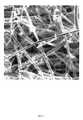
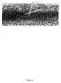
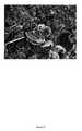
- FIG. 1shows a multitude of nanowires. These fibers were grown with H 2 /N 2 ratio of 0.005, pressure of 30 Torr and microwave power of 1000W;
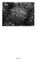
- FIG. 2shows silicon nanofibers for short time scale growth (initial one hour);
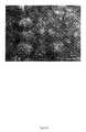
- FIGS. 3shows a silicon nanoneedle after a growth experiment for 3 hours. H 2 /N 2 ratio was kept at 0.008. Chamber pressure was 40 Torr and 800 W of microwave power was applied;
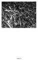
- FIG. 4shows a web of fibers grown for a longer time, five hours. Due to the long growth duration, the grown wires were very long and intermingled;
- FIG. 5shows a multitude of oriented silicon fibers. These fibers were grown with H 2 /N 2 ratio of 0.0075, pressure of 50 Torr and 1000 W of microwave power;
- FIG. 6is a schematic of the reaction chamber
- FIG. 7shows silicon Nanowires grown using our Ga and plasma mediated VLS process wherein the silicon nanowires ( ⁇ 10 nm size) growing as a multitude of filaments after a growth experiment for 8 hours with a microwave power of 600 W, 30 torr pressure, and a total flow rate of 100 sccm of hydrogen;
- FIG. 8shows silicon nanorods 150 nm thick, grown out of large gallium pool after a growth experiment for 5 hours with a microwave power of 900 W, 50 torr pressure, and a total flow rate of ⁇ 100 sccm of hydrogen with inlet H 2 /N 2 ratio of 0.75;
- FIG. 9illustrates oriented growth of silicon nanowires ⁇ 100 nm thick, using pools of gallium melt employing experimental conditions of a microwave power of 850 W, Pressure of 50 torr, growth duration of 5 hrs, and inlet H 2 /N 2 ratio of 0.75;
- FIG. 10shows bulk quantities of silicon nanowires produced after a growth experiment for 5 hours with microwave power of 900 W, pressure of 50 torr, and a total flow rate of 100 sccm of hydrogen;
- FIG. 11shows spaghetti like wires grown out of a different gallium droplet on the same substrate as processed in FIG. 10 ;
- FIG. 12shows bulk quantities of very straight silicon nanowires grown using the process of the present invention wherein the growth conditions utilized 1000 W microwave power, 50 torr pressure, growth duration of 6 hours, total gas flow rate of ⁇ 100 sccm with inlet H 2 /N 2 ratio of 0.75;
- FIG. 13shows a higher magnification SEM image of the wires grown out of a different droplet on the same substrate as in FIG. 12 ;
- FIG. 14demonstrates nucleation of multiple sub-micron and nano-scale, silicon wires from a single gallium droplet wherein the growth conditions utilized 1000 W power, 30 torr, 3 hrs duration, and H 2 /N 2 : 0.25;
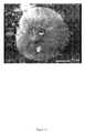
- FIG. 15shows SEM image of multiple nanowires 50 nm thick growing out of a single large gallium droplet wherein the growth conditions used 950 W power, 50 torr pressure, 7 hrs duration and H 2 /N 2 of 0.95;
- FIG. 16shows a low magnification Transmission Electron Microscope image of a web of silicon nanowires grown under the same conditions as the sample shown in FIG. 7 ;
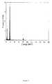
- FIG. 17shows a typical Energy Dispersive Spectroscopy spectrum taken from an individual nanowires, confirming the nanowires to be composed of silicon with some surface native oxide;
- FIG. 18shows a high Resolution Transmission Electron Microscopy (HRTEM) image of a 4 nm thick silicon nanowires wherein the lattice spacing matches that of bulk silicon;
- HRTEMHigh Resolution Transmission Electron Microscopy
- FIG. 19shows a high Resolution Transmission Electron Microscopy (HRTEM) image of a 4 nm thick silicon nanowires wherein the lattice spacing matches that of bulk silicon;
- HRTEMHigh Resolution Transmission Electron Microscopy
- FIG. 20shows multiple gallium oxide rods growing out of a large gallium pool with growth conditions of 4 hour growth duration, 1000 W microwave power, 30 Torr pressure, 100 sccm of hydrogen, 0.6 sccm of oxygen in the inlet stream;
- FIG. 21shows highly faceted gallium oxide fibers on the same sample shown in FIG. 20 ;
- FIG. 22shows gallium oxide sub-micron thick fibers in addition to the micron-scale rods in the same sample mentioned above;
- FIG. 23shows a zoomed-out view of the quartz substrate wherein multiple fibers have been grown out of a large gallium pool
- FIG. 24shows gallium oxide nanowires about 100 nm thick from a different region on the same sample as shown in FIG. 20 ;
- FIG. 25is another illustration of multiple nucleation and fiber growth
- FIG. 26shows a scanning electron microscopy image of gallium oxide platelets and crystals obtained in addition to the one-dimensional structures after a growth experiment under the same conditions as for sample in FIG. 20 , whereby growth of gallium oxide can also be achieved with a range of above-mentioned process parameters and with different substrate materials;
- FIG. 27shows a scanning electron microscopy image of gallium oxide platelets and crystals obtained in addition to the one-dimensional structures after a growth experiment under the same conditions as for sample in FIG. 20 , whereby growth of gallium oxide can also be achieved with a range of above-mentioned process parameters and with different substrate materials;
- FIG. 28shows a scanning electron microscopy image of gallium oxide platelets and crystals obtained in addition to the one-dimensional structures after a growth experiment under the same conditions as for sample in FIG. 20 , whereby growth of gallium oxide can also be achieved with a range of above-mentioned process parameters and with different substrate materials;
- FIG. 29shows a scanning electron microscopy image of gallium oxide platelets and crystals obtained in addition to the one-dimensional structures after a growth experiment under the same conditions as for sample in FIG. 20 , whereby growth of gallium oxide can also be achieved with a range of above-mentioned process parameters and with different substrate materials;
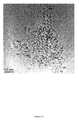
- FIG. 30shows a micrograph of carbon nanofibers of various thickness and length wherein the growth Conditions utilized a microwave power of 700 W, pressure of 40 torr, 4 hr duration, 100 sccm of hydrogen and 2 sccm of methane in the plasma; however these process parameters can be varied and synthesis of carbon nanowires obtained;
- FIG. 31shows a micrograph of carbon nanofibers of various thickness and length wherein the growth Conditions utilized a microwave power of 700 W, pressure of 40 torr, 4 hr duration, 100 sccm of hydrogen and 2 sccm of methane in the plasma; however these process parameters can be varied and synthesis of carbon nanowires obtained;
- FIG. 32shows a micrograph of carbon nanofibers of various thickness and length wherein the growth Conditions utilized a microwave power of 700 W, pressure of 40 torr, 4 hr duration, 100 sccm of hydrogen and 2 sccm of methane in the plasma; however these process parameters can be varied and synthesis of carbon nanowires obtained; and
- FIG. 33shows a micrograph of carbon nanofibers of various thickness and length wherein the growth Conditions utilized a microwave power of 700 W, pressure of 40 torr, 4 hr duration, 100 sccm of hydrogen and 2 sccm of methane in the plasma; however these process parameters can be varied and synthesis of carbon nanowires obtained.
- This inventionprovides a novel synthesis route for growing one-dimensional structures of semiconductor materials in wire, whisker and rod shapes at temperatures well under 550° C., preferably less than 300° C.
- This low-temperature synthesisis made possible by the use of gallium as a preferable absorption site.
- Galliumhas a low melting temperature ( ⁇ 30° C.) and broad temperature range for the melt phase (30–2400° C. at 1 atm).
- Indiumwhich has a melting temperature of 156.6° C., and a melt range of 156.6 to 2000° C., is also useful as a dissolution medium.
- growth of silicon fiberswas observed when silicon substrates covered with a thin film of gallium were exposed to mixture of nitrogen and hydrogen in a microwave-generated plasma.
- the resulting silicon wiresranged from several microns to less than ten (10) nanometers in diameter.
- the observed growth rateswere on the order of 100 microns/hour. Results indicate that this technique is capable of producing oriented rods and whiskers with narrow diameter distributions.
- the growth mechanism in this methodis hypothesized to be similar to that in other VLS process, i.e., rapid dissolution of silicon solute in gallium melt, formation of nuclei, nuclei surfacing out of the gallium melt, growth of silicon in one dimension in the form of fibers.
- a silicon substrate (2 cm ⁇ 2 cm)was prepared by cleaning with a 45% HF solution, thoroughly rinsing in acetone and ultra-sonication. Droplets of gallium metal at 70° C. were applied to form a film with a thickness of approximately 100 microns.
- the nitrogen flow ratewas set to 100 sccm.
- the pressure in the reactorwas set to 30 Torr. Microwaves at 2.45 Ghz were used to ionize the nitrogen gas.
- the input microwave powerwas 1000W.
- the experimentswere done in an ASTeX model 5010 bell jar reactor chamber equipped with an ASTeX model 2115 1500 W microwave power generator. 0.5 sccm of hydrogen were introduced into the nitrogen plasma. The reaction was carried out for six hours. Graphite blocks were used as substrate stage.
- FIG. 6shows a schematic of the reactor. After the growth experiments, the silicon substrate covered with an ashy mass was observed under a scanning electron microscope (SEM).
- FIGS. 1 through 16show micrographs of silicon fibers of various thickness and length.
- FIG. 1shows a group of nanowires. These fibers were grown with H 2 /N 2 ratio of 0.005, pressure of 30 Torr and microwave power of 1000W.
- FIG. 2shows silicon nanofibers for short time scale growth (initial one hour).
- FIG. 3shows a silicon nanoneedle. H 2 /N 2 ratio was kept at 0.008. Chamber pressure was 40 Torr and 800 W of microwave power was applied.
- FIG. 4shows a web of fibers grown for a longer time, five hours.
- FIG. 5shows a multitude of oriented silicon fibers. These fibers were grown with H 2 /N 2 ratio of 0.0075, pressure of 50 Torr and 1000 W of microwave power.
- FIG. 7shows silicon Nanowires grown using the instant Ga and plasma mediated VLS process. Silicon nanowires ( ⁇ 10 nm size) growing as a multitude of filaments after a growth experiment for 8 hours with a microwave power of 600 W, 30 torr pressure, and a total flow rate of 100 sccm of hydrogen.
- FIG. 8shows oriented silicon nanorods 150 nm thick, grown out of large gallium pool after a growth experiment for 5 hours with a microwave power of 900 W, 50 torr pressure, and a total flow rate of ⁇ 100 sccm of hydrogen with inlet H 2 /N 2 ratio of 0.0075.
- FIG. 9illustrates oriented growth of silicon nanowires ⁇ 100 nm thick, using large pools of gallium melt. These nanowires were grown for 5 hours with microwave power of 850 W, Pressure of 50 torr, and inlet H 2 /N 2 ratio of 0.0075.
- FIG. 8shows oriented silicon nanorods 150 nm thick, grown out of large gallium pool after a growth experiment for 5 hours with a microwave power of 900 W, 50 torr pressure, and a total flow rate of ⁇ 100 sccm of hydrogen with inlet H 2 /N 2 ratio of 0.0075.
- FIG. 9illustrates oriented growth of silicon nanowires ⁇ 100 nm thick, using
- FIG. 10shows profuse quantities of silicon nanowires produced after a growth experiment for 5 hours with microwave power of 900 W, pressure of 50 torr, and a total flow rate of 100 sccm of hydrogen.
- the nanowireswere imaged using a Hitachi 3200N scanning electron microscope at an acceleration voltage of 20 kV and a magnification of ⁇ 7 k.
- FIG. 11shows spaghetti like wires grown out of a different gallium droplet on the same sample as in FIG. 10 .
- FIG. 12shows bulk quantities of very straight silicon nanofilaments grown for 6 hours with 1000 W microwave power, 50 torr pressure, and a total gas flow rate of 100 sccm with inlet H 2 /N 2 ratio of 0.0075.
- FIG. 13shows a higher magnification SEM image of the wires grown out of a different droplet on the same substrate as in FIG. 12 .
- FIG. 14demonstrates the fact that multiple nanowires can nucleate and grow out of a large gallium pool in our technique, unlike in traditional VLS techniques, where one has to create nanometer sized catalyst particles. Multiple sub-micron and nano-scale silicon wires are shown to grow out of a single large gallium droplet. These fibers were grown for 3 hours with 1000 W microwave power, 30 torr, and H 2 /N 2 ratio of 0.0025.
- FIG. 15shows SEM image of multiple nanowires 50 nm thick growing out of a single large gallium droplet.
- FIG. 16shows a web of silicon nanowires grown under the same conditions as the sample shown in FIG. 7 . These nanowires imaged using a JEOL 2000FX Transmission Electron Microscope at an acceleration voltage of 200 kV and a magnification of ⁇ 300 k. The elemental composition of the fibrous structures was determined using Energy Dispersive Spectroscopy (EDX), a feature in the JEOL 2000FX microscope.
- FIG. 17shows a representative EDX spectrum of an individual nanowires shown in FIG. 16 . The nanowires composed of silicon, with some surface oxidation.
- FIGS. 18 and 19represent high resolution Transmission Electron Microscopy images of two different silicon nanowires about 4 nm thick. The fringes in these micrographs represent lattice planes in the nanowires. The lattice spacing was measured using the Digital Micrograph software, which matched the values for bulk silicon lattice spacings.
- Gallium oxide fiberscan be grown using the above plasma mediated technique.
- a quartz substrate (2 cm ⁇ 2 cm)was prepared by ultra-sonication in IsoPropyl Alcohol. Droplets of gallium metal at 70° C. were applied to form a film with a thickness of approximately 100 microns.
- the hydrogen flow ratewas set to 100 sccm.
- the pressure in the reactorwas set to 40 Torr. Microwaves at 2.45 Ghz were used to ionize the hydrogen gas.
- the input microwave powerwas 700W.
- the experimentswere done in an ASTeX model 5010 bell jar reactor chamber equipped with an ASTeX model 2115 1500 W microwave power generator. 0.6 sccm of oxygen were introduced into the hydrogen plasma. The reaction was carried out for four hours.
- FIGS. 20 through 25show micrographs of gallium oxide fibers of various thickness and length.
- FIG. 20shows multiple gallium oxide rods growing out of a large gallium pool. The fibers are very well faceted and were grown for 4 hours with 1000 W microwave power, 30 Torr pressure, 100 sccm of hydrogen, and 0.6 sccm of oxygen in the inlet stream.
- FIG. 21shows highly faceted gallium oxide fibers on the same sample shown in FIG. 20 .
- the micrographswere taken using a LEO 1430 Scanning Electron Microscope at an acceleration voltage of 20 kV.
- FIG. 22shows gallium oxide sub-micron thick fibers in addition to the micron-scale rods in the same sample mentioned above.
- FIG. 23shows an overall zoomed out view of the quartz substrate, demonstrating the fact that multiple fibers can nucleate and grow out of a large gallium pool using our technique.
- FIG. 24shows gallium oxide nanowires about 100 nm thick from a different region on the same sample as shown in FIG. 20 .
- FIG. 25is another illustration of multiple nucleation and fiber growth. In addition to the one-dimensional structures, we also observed gallium oxide platelets about 100–200 nm thick, as shown in FIGS. 26 through 29 .
- Gallium oxide fiberswere also synthesized with gallium droplets spread on other substrates, such as pyrolytic boron nitride, alumina, and glassy carbon. In addition to different fractions of O 2 /H 2 being used, fractions of methane and nitrogen were also introduced into the plasma and synthesis of gallium oxide fibers was obtained.
- Carbon nanofibershave been grown using the above plasma-mediated technique.
- a pyrolytic boron nitride substrate( ⁇ 1 cm ⁇ 1 cm) was prepared by ultra-sonication in IsoPropyl Alcohol. The substrate was covered with molten gallium droplets.
- the hydrogen flow ratewas set to 100 sccm.
- the pressure in the reactorwas set to 40 Torr. Microwaves at 2.45 Ghz were used to ionize the hydrogen gas.
- the input microwave powerwas 700W.
- the experimentswere done in an ASTeX model 5010 bell jar reactor chamber equipped with an ASTeX model 2115 1500 W microwave power generator. 2.0 sccm of methane were introduced into the hydrogen plasma. The reaction was carried out for four hours.
- FIGS. 30 through 33show micrographs of carbon nanofibers of various thickness and length.
- FIG. 30shows multiple carbon filaments growing out of a large gallium droplet.
- FIG. 31shows a higher magnification image of approximately 50 nm thick nanofilaments.
- Germanium fiberscan be grown using the above technique by using either germanium substrate or using germane in the vapor phase.
- the gas phasewill preferably consist of hydrogen with or without nitrogen to result in the formation of germane radicals, a gaseous source of germanium. Germane will be decomposed on the gallium substrate resulting in dissolution of germanium into the gallium melt.
- Nitrogencan also be dissolved into gallium melt, but at relatively higher temperatures than above, i.e., above ⁇ 600° C. At these temperatures, using gallium droplets exposed to an atomic nitrogen source, such as plasma, one can achieve nitrogen saturated gallium melts. These nitrogen saturated gallium melts will form gallium nitride either in the whisker or nanowire form.
- gallium dropletUsing a similar setup as that used for example 1, one can expose the gallium droplet to nitrogen and hydrogen plasma at relatively higher temperature, i.e., ⁇ 600° C., to achieve the dissolution of both nitrogen and silicon into the gallium droplet.
Landscapes
- Engineering & Computer Science (AREA)
- Chemical & Material Sciences (AREA)
- Nanotechnology (AREA)
- Manufacturing & Machinery (AREA)
- Materials Engineering (AREA)
- Crystallography & Structural Chemistry (AREA)
- Chemical Kinetics & Catalysis (AREA)
- Condensed Matter Physics & Semiconductors (AREA)
- General Physics & Mathematics (AREA)
- Physics & Mathematics (AREA)
- Textile Engineering (AREA)
- General Chemical & Material Sciences (AREA)
- Ceramic Engineering (AREA)
- Inorganic Chemistry (AREA)
- Composite Materials (AREA)
- Structural Engineering (AREA)
- Organic Chemistry (AREA)
- Crystals, And After-Treatments Of Crystals (AREA)
- Silicon Compounds (AREA)
- Inorganic Fibers (AREA)
Abstract
Description
Claims (22)
Priority Applications (4)
| Application Number | Priority Date | Filing Date | Title |
|---|---|---|---|
| US10/187,460US7252811B2 (en) | 2000-06-29 | 2002-07-01 | Low temperature synthesis of silicon fibers |
| US10/869,489US7445671B2 (en) | 2000-06-29 | 2004-06-16 | Formation of metal oxide nanowire networks (nanowebs) of low-melting metals |
| US11/515,051US7241432B2 (en) | 2000-06-29 | 2006-09-01 | Low temperature synthesis of semiconductor fibers |
| US11/521,084US7713352B2 (en) | 2001-06-29 | 2006-09-14 | Synthesis of fibers of inorganic materials using low-melting metals |
Applications Claiming Priority (4)
| Application Number | Priority Date | Filing Date | Title |
|---|---|---|---|
| US21496300P | 2000-06-29 | 2000-06-29 | |
| US30206201P | 2001-06-29 | 2001-06-29 | |
| US09/896,834US6806228B2 (en) | 2000-06-29 | 2001-06-29 | Low temperature synthesis of semiconductor fibers |
| US10/187,460US7252811B2 (en) | 2000-06-29 | 2002-07-01 | Low temperature synthesis of silicon fibers |
Related Parent Applications (2)
| Application Number | Title | Priority Date | Filing Date |
|---|---|---|---|
| US89683400AContinuation-In-Part | 2000-06-29 | 2000-06-29 | |
| US09/896,834Continuation-In-PartUS6806228B2 (en) | 2000-06-29 | 2001-06-29 | Low temperature synthesis of semiconductor fibers |
Related Child Applications (3)
| Application Number | Title | Priority Date | Filing Date |
|---|---|---|---|
| US10/664,072Continuation-In-PartUS7182812B2 (en) | 2000-06-29 | 2003-09-16 | Direct synthesis of oxide nanostructures of low-melting metals |
| US11/515,051ContinuationUS7241432B2 (en) | 2000-06-29 | 2006-09-01 | Low temperature synthesis of semiconductor fibers |
| US11/521,084Continuation-In-PartUS7713352B2 (en) | 2001-06-29 | 2006-09-14 | Synthesis of fibers of inorganic materials using low-melting metals |
Publications (2)
| Publication Number | Publication Date |
|---|---|
| US20030039602A1 US20030039602A1 (en) | 2003-02-27 |
| US7252811B2true US7252811B2 (en) | 2007-08-07 |
Family
ID=37589772
Family Applications (2)
| Application Number | Title | Priority Date | Filing Date |
|---|---|---|---|
| US10/187,460Expired - LifetimeUS7252811B2 (en) | 2000-06-29 | 2002-07-01 | Low temperature synthesis of silicon fibers |
| US11/515,051Expired - LifetimeUS7241432B2 (en) | 2000-06-29 | 2006-09-01 | Low temperature synthesis of semiconductor fibers |
Family Applications After (1)
| Application Number | Title | Priority Date | Filing Date |
|---|---|---|---|
| US11/515,051Expired - LifetimeUS7241432B2 (en) | 2000-06-29 | 2006-09-01 | Low temperature synthesis of semiconductor fibers |
Country Status (1)
| Country | Link |
|---|---|
| US (2) | US7252811B2 (en) |
Cited By (2)
| Publication number | Priority date | Publication date | Assignee | Title |
|---|---|---|---|---|
| US20070095276A1 (en)* | 2001-06-29 | 2007-05-03 | Sunkara Mahendra K | Synthesis of fibers of inorganic materials using low-melting metals |
| US9630162B1 (en) | 2007-10-09 | 2017-04-25 | University Of Louisville Research Foundation, Inc. | Reactor and method for production of nanostructures |
Families Citing this family (11)
| Publication number | Priority date | Publication date | Assignee | Title |
|---|---|---|---|---|
| US7182812B2 (en)* | 2002-09-16 | 2007-02-27 | University Of Louisville | Direct synthesis of oxide nanostructures of low-melting metals |
| US7238232B1 (en)* | 2002-04-30 | 2007-07-03 | University Of Louisville | Growth of textured gallium nitride thin films on polycrystalline substrates |
| US7241479B2 (en)* | 2003-08-22 | 2007-07-10 | Clemson University | Thermal CVD synthesis of nanostructures |
| DE10345157B4 (en)* | 2003-09-29 | 2009-01-08 | Qimonda Ag | Thermally conductive packaging of electronic circuit units |
| JP2007526200A (en)* | 2004-01-14 | 2007-09-13 | ザ リージェンツ オブ ザ ユニヴァーシティ オブ カリフォルニア | Diluted magnetic semiconductor nanowires exhibiting magnetoresistance |
| US7662355B2 (en)* | 2004-11-29 | 2010-02-16 | National University Corporation Tokyo University Of Agriculture And Technology | Silicon nanosized linear body and a method for producing a silicon nanosized linear body |
| US7442575B2 (en)* | 2006-09-29 | 2008-10-28 | Texas Christian University | Method of manufacturing semiconductor nanowires |
| JP5363343B2 (en)* | 2007-02-19 | 2013-12-11 | アイメック | Low temperature formation of polycrystalline semiconductor material layers |
| US8603246B2 (en)* | 2008-01-30 | 2013-12-10 | Palo Alto Research Center Incorporated | Growth reactor systems and methods for low-temperature synthesis of nanowires |
| JP4344002B1 (en) | 2008-10-27 | 2009-10-14 | 株式会社新川 | Wire bonding method |
| JP4867981B2 (en)* | 2008-12-04 | 2012-02-01 | 住友電気工業株式会社 | GaN crystal growth method |
Citations (15)
| Publication number | Priority date | Publication date | Assignee | Title |
|---|---|---|---|---|
| US4886683A (en) | 1986-06-20 | 1989-12-12 | Raytheon Company | Low temperature metalorganic chemical vapor depostion growth of group II-VI semiconductor materials |
| JPH0286121A (en) | 1988-09-22 | 1990-03-27 | Toshiba Corp | Compound semiconductor vapor phase growth equipment |
| US4939308A (en)* | 1988-04-29 | 1990-07-03 | Allied-Signal Inc. | Method of forming crystallite-oriented superconducting ceramics by electrodeposition and thin film superconducting ceramic made thereby |
| US5120707A (en)* | 1989-05-22 | 1992-06-09 | Allied-Signal, Inc. | Superconducting ceramics by electrodeposition of metals with embedment of particulate matter, followed by oxidation |
| US5334296A (en) | 1992-01-15 | 1994-08-02 | Andcare, Inc. | Peroxidase colloidal gold oxidase biosensors for mediatorless glucose determination |
| US5381753A (en) | 1992-04-30 | 1995-01-17 | Matsushita Electric Industrial Co., Ltd. | Fabrication method of fine structures |
| US5725674A (en) | 1991-03-18 | 1998-03-10 | Trustees Of Boston University | Device and method for epitaxially growing gallium nitride layers |
| US5858862A (en) | 1996-09-25 | 1999-01-12 | Sony Corporation | Process for producing quantum fine wire |
| JPH11177134A (en) | 1997-12-15 | 1999-07-02 | Sharp Corp | Method for manufacturing semiconductor element and semiconductor element, and method for manufacturing light emitting element and light emitting element |
| US5922183A (en) | 1997-06-23 | 1999-07-13 | Eic Laboratories, Inc. | Metal oxide matrix biosensors |
| US5962863A (en) | 1993-09-09 | 1999-10-05 | The United States Of America As Represented By The Secretary Of The Navy | Laterally disposed nanostructures of silicon on an insulating substrate |
| US6033866A (en) | 1997-12-08 | 2000-03-07 | Biomedix, Inc. | Highly sensitive amperometric bi-mediator-based glucose biosensor |
| US6051849A (en) | 1998-02-27 | 2000-04-18 | North Carolina State University | Gallium nitride semiconductor structures including a lateral gallium nitride layer that extends from an underlying gallium nitride layer |
| US6063246A (en) | 1997-05-23 | 2000-05-16 | University Of Houston | Method for depositing a carbon film on a membrane |
| US6806228B2 (en)* | 2000-06-29 | 2004-10-19 | University Of Louisville | Low temperature synthesis of semiconductor fibers |
- 2002
- 2002-07-01USUS10/187,460patent/US7252811B2/ennot_activeExpired - Lifetime
- 2006
- 2006-09-01USUS11/515,051patent/US7241432B2/ennot_activeExpired - Lifetime
Patent Citations (15)
| Publication number | Priority date | Publication date | Assignee | Title |
|---|---|---|---|---|
| US4886683A (en) | 1986-06-20 | 1989-12-12 | Raytheon Company | Low temperature metalorganic chemical vapor depostion growth of group II-VI semiconductor materials |
| US4939308A (en)* | 1988-04-29 | 1990-07-03 | Allied-Signal Inc. | Method of forming crystallite-oriented superconducting ceramics by electrodeposition and thin film superconducting ceramic made thereby |
| JPH0286121A (en) | 1988-09-22 | 1990-03-27 | Toshiba Corp | Compound semiconductor vapor phase growth equipment |
| US5120707A (en)* | 1989-05-22 | 1992-06-09 | Allied-Signal, Inc. | Superconducting ceramics by electrodeposition of metals with embedment of particulate matter, followed by oxidation |
| US5725674A (en) | 1991-03-18 | 1998-03-10 | Trustees Of Boston University | Device and method for epitaxially growing gallium nitride layers |
| US5334296A (en) | 1992-01-15 | 1994-08-02 | Andcare, Inc. | Peroxidase colloidal gold oxidase biosensors for mediatorless glucose determination |
| US5381753A (en) | 1992-04-30 | 1995-01-17 | Matsushita Electric Industrial Co., Ltd. | Fabrication method of fine structures |
| US5962863A (en) | 1993-09-09 | 1999-10-05 | The United States Of America As Represented By The Secretary Of The Navy | Laterally disposed nanostructures of silicon on an insulating substrate |
| US5858862A (en) | 1996-09-25 | 1999-01-12 | Sony Corporation | Process for producing quantum fine wire |
| US6063246A (en) | 1997-05-23 | 2000-05-16 | University Of Houston | Method for depositing a carbon film on a membrane |
| US5922183A (en) | 1997-06-23 | 1999-07-13 | Eic Laboratories, Inc. | Metal oxide matrix biosensors |
| US6033866A (en) | 1997-12-08 | 2000-03-07 | Biomedix, Inc. | Highly sensitive amperometric bi-mediator-based glucose biosensor |
| JPH11177134A (en) | 1997-12-15 | 1999-07-02 | Sharp Corp | Method for manufacturing semiconductor element and semiconductor element, and method for manufacturing light emitting element and light emitting element |
| US6051849A (en) | 1998-02-27 | 2000-04-18 | North Carolina State University | Gallium nitride semiconductor structures including a lateral gallium nitride layer that extends from an underlying gallium nitride layer |
| US6806228B2 (en)* | 2000-06-29 | 2004-10-19 | University Of Louisville | Low temperature synthesis of semiconductor fibers |
Non-Patent Citations (17)
| Title |
|---|
| A M Morales and C.M. Lieber "A Laser Ablation Method for the Synthesis of Crystalline Semiconductor Nanowires", Science, vol. 279, Jan. 9, 1998. 208 211. |
| D.P. Yu, Y.J Xing, Q.L. Hang, H.F Yan. J Xu, Z H. Xi, S.Q. Feng "Controlled Growth of Oriented Amorphous Silicon Nanowires Via A Solid-Liquid-Solid (SLS) Mechanism", Physica E 9 (2001) 305-309. |
| D.P. Yu, Z.G. Bai, Y. Ding, Q.L. Hang, H.Z. Zhang, J.J. Wang, Y.H. Zou, W. Qian, G.C. Xiong, H.T. Zhou, and S.Q. Feng "Nanoscale Silicon Wires Synthesized Using Simple Physical Evaporation", Applied Physics Letters, vol. 72, No. 26, Jun. 29, 1998, 3458-3460. |
| H.F. Yan, Y.J. Xing, Q.L. Hang, D.P. Yu, Y.P. Wang, J. Xu, Z.H. Xi, S.Q. Feng "Growth of Amorphous Silicon Nanowires Via A Solid-Liquid-Solid Mechanism", Chemical Physics Letters 323 (2000) 224-228. |
| J. Westwater, D.P. Gosain, S. Tomiya, S. Usui, and H. Ruda "Growth of Silicon Nanowires Via Gold/Silane Vapor-Liquid-Solid Reaction", J. Vac. Sci. Technol. B 15(3), May/Jun. 1997, 554-557. |
| J.D. Holmes, K.P. Johnston, R.C. Doty, B. A. Korgel "Control of Thickness and Orientation of Solution-Grown Silicon Nanowires", Science, vol. 287, Feb. 25, 2000, 1471-1473. |
| J.L. Gole and J.D. Stout, W.L. Rauch and Z.L. Wang "Direct Synthesis of Silicon Nanowires, Silica Nanospheres, and Wire-Like Nanosphere Agglomerates", Applied Physics Letters, vol. 76, No. 17, Apr. 24, 2000, 2346-2348. |
| Lieber, "One-Dimensional Nanostructures: Chemistry, Physics & Applications", Solid State Communications. vol. 107, No. 11 607-616. |
| P Scheier, J. Marsen, M Lonfat, W Schneider, K. Sattler "Growth of Silicon Nanostructures on Graphite", Surface Science 458 (2000, 113-122. |
| Publication No. WO026422A1 for "High Purity Gallium for Preparation of Compound Semiconductor, and Method and Apparatus for Purifying the Same" by Yamamura et al., published on May 11, 2000. |
| Publication No. WO9944224A1 for "Method of Fabricating Gallium Nitride Semiconductor Layers by Lateral Overgrowth Through Masks, and Gallium Nitride Semiconductor Structures Fabricated Thereby" by Davis et al., published on Sep. 2, 1999. |
| Publication No. WO9965068A1 for "Fabrication of Gallium Nitride Semiconductor Layers by Lateral Growth from Trench Sidewalls" by Zheleva et al., published on Dec. 16, 1999. |
| Sharma et al "Novel Vapor-Liquid-Solid Synthesis Method for Carbon Nanostructures", presented on CD and at Carbon2001 Conference at the University of Kentucky, Lexington, KY in Jul. of 2001. |
| Wu et al. "Germanium Nanowire Growth Via Simple Vapor Transport", Chem. Mater. 2000, 12, 605-607. |
| Y.F. Zhang, Y H Tanh, N. Wang, D.P. Yu. C S Lee, I. Bello, and S.T. Lee "Silicon Nanowires Prepared by Laser Ablation at High Temperature", Applied Physics Letters, vol. 72, No. 15, Apr. 13, 1998, 1835-1837. |
| Y.F. Zhang, Y.H. Tang, N. Wang, C.S. Lee, I. Bello, S.T. Lee "One-Dimensional Growth Mechanism of Crystalline Silicon Nanowires", Journal of Crystal Growth 197 (1999) 136-140. |
| Zhang et al "Morphology and Growth Mechanism Study of Self-Assembled Silicon Nanowires Synthesized by Thermal Evaporation", Chemical Physics Letters 337 (2001) 18-24, Mar. 30, 2001. |
Cited By (3)
| Publication number | Priority date | Publication date | Assignee | Title |
|---|---|---|---|---|
| US20070095276A1 (en)* | 2001-06-29 | 2007-05-03 | Sunkara Mahendra K | Synthesis of fibers of inorganic materials using low-melting metals |
| US7713352B2 (en)* | 2001-06-29 | 2010-05-11 | University Of Louisville Research Foundation, Inc. | Synthesis of fibers of inorganic materials using low-melting metals |
| US9630162B1 (en) | 2007-10-09 | 2017-04-25 | University Of Louisville Research Foundation, Inc. | Reactor and method for production of nanostructures |
Also Published As
| Publication number | Publication date |
|---|---|
| US20030039602A1 (en) | 2003-02-27 |
| US20070003467A1 (en) | 2007-01-04 |
| US7241432B2 (en) | 2007-07-10 |
Similar Documents
| Publication | Publication Date | Title |
|---|---|---|
| US7241432B2 (en) | Low temperature synthesis of semiconductor fibers | |
| US7713352B2 (en) | Synthesis of fibers of inorganic materials using low-melting metals | |
| Shi et al. | Microstructures of gallium nitride nanowires synthesized by oxide-assisted method | |
| Zhang et al. | Germanium nanowires sheathed with an oxide layer | |
| Zhang et al. | A simple method to synthesize Si3N4 and SiO2 nanowires from Si or Si/SiO2 mixture | |
| US6806228B2 (en) | Low temperature synthesis of semiconductor fibers | |
| US6313015B1 (en) | Growth method for silicon nanowires and nanoparticle chains from silicon monoxide | |
| JP3183845B2 (en) | Method for producing carbon nanotube and carbon nanotube film | |
| CN1248959C (en) | Carbon nano pipe array growth method | |
| KR101591441B1 (en) | Process for producing boron nitride nanotubes | |
| Mårtensson et al. | Fabrication of individually seeded nanowire arrays by vapour–liquid–solid growth | |
| Ozaki et al. | Silicon nanowhiskers grown on a hydrogen-terminated silicon {111} surface | |
| Zhang et al. | Synthesis of thin Si whiskers (nanowires) using SiCl4 | |
| Han et al. | Controlled growth of gallium nitride single-crystal nanowires using a chemical vapor deposition method | |
| US9676627B2 (en) | Growth of silicon and boron nitride nanomaterials on carbon fibers by chemical vapor deposition | |
| KR100785347B1 (en) | Alignment method of semiconductor nanowire on metal electrode | |
| CN101553895A (en) | One-dimensional metal and metal oxide nanostructures | |
| CN101062765A (en) | A kind of preparation method of quasi-one-dimensional boron nitride nanostructure | |
| Liu et al. | Synthesis of silicon nanowires using AuPd nanoparticles catalyst on silicon substrate | |
| US20070235841A1 (en) | Silicon nanowire structure and method for making same | |
| Hamidinezhad et al. | Influence of growth time on morphology and structural properties of silicon nanowires grown by VHF-PECVD | |
| KR20050010601A (en) | Synthesis of ZnO Nano-structured material, and its apparatus | |
| CN100415952C (en) | Method for Synthesizing Ordered Arrays of Small Diameter Single Crystal SiC Nanofilaments by Thermal Evaporation | |
| Li et al. | Synthesis of ordered Si nanowire arrays in porous anodic aluminum oxide templates | |
| JP3911564B2 (en) | Boron nitride nanocomposite structure and manufacturing method thereof |
Legal Events
| Date | Code | Title | Description |
|---|---|---|---|
| AS | Assignment | Owner name:UNIVERSITY OF LOUISVILLE, KENTUCKY Free format text:ASSIGNMENT OF ASSIGNORS INTEREST;ASSIGNORS:SHARMA, SHASHANK;SUNKARA, MAHENDRA KUMAR;REEL/FRAME:013492/0047 Effective date:20021028 | |
| AS | Assignment | Owner name:AIR FORCE, UNITED STATES, VIRGINIA Free format text:CONFIRMATORY LICENSE;ASSIGNOR:LOUISVILLE, UNIVERSITY OF;REEL/FRAME:017420/0967 Effective date:20050603 | |
| STCF | Information on status: patent grant | Free format text:PATENTED CASE | |
| AS | Assignment | Owner name:UNIVERSITY OF LOUISVILLE RESEARCH FOUNDATION, INC. Free format text:ASSIGNMENT OF ASSIGNORS INTEREST;ASSIGNOR:UNIVERSITY OF LOUISVILLE;REEL/FRAME:021311/0526 Effective date:20080729 | |
| FPAY | Fee payment | Year of fee payment:4 | |
| FEPP | Fee payment procedure | Free format text:PATENT HOLDER CLAIMS MICRO ENTITY STATUS, ENTITY STATUS SET TO MICRO (ORIGINAL EVENT CODE: STOM); ENTITY STATUS OF PATENT OWNER: SMALL ENTITY Free format text:PETITION RELATED TO MAINTENANCE FEES FILED (ORIGINAL EVENT CODE: PMFP); ENTITY STATUS OF PATENT OWNER: SMALL ENTITY Free format text:PETITION RELATED TO MAINTENANCE FEES GRANTED (ORIGINAL EVENT CODE: PMFG); ENTITY STATUS OF PATENT OWNER: SMALL ENTITY | |
| REMI | Maintenance fee reminder mailed | ||
| PRDP | Patent reinstated due to the acceptance of a late maintenance fee | Effective date:20150818 | |
| FPAY | Fee payment | Year of fee payment:8 | |
| MAFP | Maintenance fee payment | Free format text:PAYMENT OF MAINTENANCE FEE, 12TH YR, SMALL ENTITY (ORIGINAL EVENT CODE: M2553); ENTITY STATUS OF PATENT OWNER: SMALL ENTITY Year of fee payment:12 |