US7252777B2 - Method of forming an in-situ recessed structure - Google Patents
Method of forming an in-situ recessed structureDownload PDFInfo
- Publication number
- US7252777B2 US7252777B2US10/946,565US94656504AUS7252777B2US 7252777 B2US7252777 B2US 7252777B2US 94656504 AUS94656504 AUS 94656504AUS 7252777 B2US7252777 B2US 7252777B2
- Authority
- US
- United States
- Prior art keywords
- film
- substrate
- recited
- projections
- forming
- Prior art date
- Legal status (The legal status is an assumption and is not a legal conclusion. Google has not performed a legal analysis and makes no representation as to the accuracy of the status listed.)
- Active, expires
Links
- PSGCQDPCAWOCSH-UHFFFAOYSA-NC=CC(=O)OC1CC2CCC1(C)C2(C)CChemical compoundC=CC(=O)OC1CC2CCC1(C)C2(C)CPSGCQDPCAWOCSH-UHFFFAOYSA-N0.000description1
- LNMQRPPRQDGUDR-UHFFFAOYSA-NC=CC(=O)OCCCCCCChemical compoundC=CC(=O)OCCCCCCLNMQRPPRQDGUDR-UHFFFAOYSA-N0.000description1
- KUDUQBURMYMBIJ-UHFFFAOYSA-NC=CC(=O)OCCOC(=O)C=CChemical compoundC=CC(=O)OCCOC(=O)C=CKUDUQBURMYMBIJ-UHFFFAOYSA-N0.000description1
- VKPVUNFNWSJTBJ-UHFFFAOYSA-NC=CC(=O)OC[Si](C)(C)O[Si](C)(C)CChemical compoundC=CC(=O)OC[Si](C)(C)O[Si](C)(C)CVKPVUNFNWSJTBJ-UHFFFAOYSA-N0.000description1
- MKLXUFCZKZGIBW-UHFFFAOYSA-NC=CC(=O)OC[Si](C)(O[Si](OC)(OC)OC)O[Si](OC)(OC)OCChemical compoundC=CC(=O)OC[Si](C)(O[Si](OC)(OC)OC)O[Si](OC)(OC)OCMKLXUFCZKZGIBW-UHFFFAOYSA-N0.000description1
- XMLYCEVDHLAQEL-UHFFFAOYSA-NCC(C)(O)C(=O)C1=CC=CC=C1Chemical compoundCC(C)(O)C(=O)C1=CC=CC=C1XMLYCEVDHLAQEL-UHFFFAOYSA-N0.000description1
Images


Classifications
- B—PERFORMING OPERATIONS; TRANSPORTING
- B81—MICROSTRUCTURAL TECHNOLOGY
- B81C—PROCESSES OR APPARATUS SPECIALLY ADAPTED FOR THE MANUFACTURE OR TREATMENT OF MICROSTRUCTURAL DEVICES OR SYSTEMS
- B81C1/00—Manufacture or treatment of devices or systems in or on a substrate
- B81C1/00436—Shaping materials, i.e. techniques for structuring the substrate or the layers on the substrate
- B81C1/00555—Achieving a desired geometry, i.e. controlling etch rates, anisotropy or selectivity
- B81C1/00626—Processes for achieving a desired geometry not provided for in groups B81C1/00563 - B81C1/00619
Definitions
- the field of inventionrelates generally to micro and/or nano-fabrication of structures. More particularly, the present invention is directed to forming relief structures in substrates.
- Micro-fabricationinvolves the fabrication of very small structures, e.g., having features on the order of micro-meters or smaller.
- One area in which micro-fabrication has a sizeable impactis in the semiconductor processing industry for the manufacture of integrated circuits. As the semiconductor processing industry continues to strive for larger production yields while increasing the circuits per unit area formed on a substrate, micro-fabrication becomes increasingly important.
- Other areas of development in which micro-fabrication has been employedinclude biotechnology, optical technology, mechanical systems and the like.
- Photolithographyincludes a combination of an exposure tool and an image transfer process.
- a process compatible masking layeroften referred to as a resist-layer, is employed to provide the desired pattern. That is, the material from which the resist-layer is fabricated is optimized for the exposure tool and the image transfer process.
- the proper resist materialincluding the exposure wavelength and compatibility of the resist-layer material to post imaging processes, e.g., subsequent etch and deposition processes.
- replicating patterns with well-defined featuresis dependent upon operational characteristics of the exposure tool. These characteristics include, and are not limited to, the numerical aperture of the exposure tool lens, wavelength employed and alignment systems.
- imprint lithographyRecently a new non-photolithographic patterning process has evolved, which is commonly referred to as imprint lithography, overcoming many of the complexities and limitations of exposure tool technology.
- imprint lithographic processesare described in detail in numerous publications, such as United States published patent application 2004/0065976, filed as U.S. patent application Ser. No. 10/264960 on Oct. 4, 2002 and entitled METHOD AND A MOLD TO ARRANGE FEATURES ON A SUBSTRATE TO REPLICATE FEATURES HAVING MINIMAL DIMENSIONAL VARIABILITY; United States published patent application 2004/0065252, filed as U.S. patent application Ser. No. 10/264926 on Oct.
- the fundamental imprint lithography technique disclosed in each of the aforementioned published patent applicationsincludes formation of a relief pattern in a polymerizable layer and transferring a pattern corresponding to the relief pattern into an underlying substrate.
- a templateis employed spaced-apart from the substrate with a formable liquid present between the template and the substrate.
- the liquidis solidified to form a solidified layer that has a pattern recorded therein that is conforming to a shape of the surface of the template in contact with the liquid.
- the substrate and the solidified layerare then subjected to processes to transfer, into the substrate, a relief image that corresponds to the pattern in the solidified layer.
- control over the dimensions of the features formed with the aforementioned processeshas been dependent upon the topology of the underlying surface in contact with the formable liquid.
- the present inventionfeatures a method of patterning a substrate that includes forming from a first material, disposed on the substrate, a first film having an original pattern that includes a plurality of projections.
- a subset of the projectionsextends from a nadir surface, terminating in an apex surface defining a height therebetween.
- a portion of the first film in superimposition with the nadir surfacedefines a nadir portion.
- the nadir portionis removed to expose a region of the substrate in superimposition therewith, defining a plurality of recessions.
- a second materialis disposed upon the first film to form a second film having a surface spaced-apart from the apex surface of the plurality of projections and filling the plurality of recessions to form a multi-film stack.
- the first film and portions of the second filmare removed to create a plurality of spaced-apart projections of the second material on the substrate.
- the dimensions of the projections of the second materialare defined by both the spacing between the projections of the first material and the height. Specifically, the height is selected so as to be greater than the height of the projections of the second material to accommodate the effects of removing the nadir portion. Specifically, the apex surface facets during removal of the nadir surface.
- the Crown surfaceincludes regions of the first material separated by regions of the second material.
- the first materialis an organic acrylate and the second material is a dielectric.
- the first materialis an organic acrylate and the second material is a conductive material.
- FIG. 1is a simplified cross-sectional view of a multi-layered structure in accordance with one embodiment of the present invention
- FIG. 2is a simplified cross-sectional view after a blanket etch of the multi-layered structure, shown in FIG. 1 , to form a crown surface in accordance with one embodiment of the present invention
- FIG. 3is a simplified cross-sectional view of the multi-layered structure, shown in FIG. 2 , after subjecting the crown surface to an etch to form recesses in portions of the substrate in accordance with one embodiment of the present invention
- FIG. 4is a simplified cross-sectional view of the multi-layer structure in accordance with an alternate embodiment
- FIG. 5is a simplified cross-sectional view of the multi-layer structure shown in FIG. 4 after being subjected to a blanket etch;
- FIG. 6is a simplified cross-sectional view of the multi-layered structure, shown in FIG. 5 , after subjecting a crown surface to an etch to form recesses in a primer layer;
- FIG. 7is a simplified cross-sectional view of the multi-layer structure shown in FIG. 6 after deposition of a second etch differential layer;
- FIG. 8is a simplified cross-sectional view of the multi-layer structure shown in FIG. 7 after being subjected to an additional blanket etch;
- FIG. 9is a simplified cross-sectional view of the multi-layer structure shown in FIG. 8 after formation of recesses employing an anisotropic etch;
- FIG. 10is a simplified cross-sectional view of a patterned layer disposed upon a substrate in accordance with one embodiment of the present invention.
- FIG. 11is a simplified cross-sectional view of a multi-layered structure, formed by deposition of an etch-differential layer upon the patterned layer, shown in FIG. 10 ;
- FIG. 12is a simplified cross-sectional view of the multi-layered structure, shown in FIG. 11 , after subjecting the same to a blanket etch to form a crown surface;
- FIG. 13is a simplified cross-sectional view of the multi-layered structure, shown in FIG. 12 after subjecting the crown surface to an etch to form via portions in the substrate in accordance with one embodiment of the present invention
- FIG. 14is a simplified cross-sectional view of the multi-layered structure, shown in FIG. 13 , after subjecting the same to an anisotropic etch to form trench portions aligned with the via portions in accordance with one embodiment of the present invention
- FIG. 15is a simplified cross-sectional view of the multi-layered structure, shown in FIG. 14 , after deposition of conductive material in the via portion and trench portion in accordance with one embodiment of the present invention
- FIG. 16is a cross-sectional view of a substrate patterned with an organic acrylate material in accordance with an alternate embodiment of the present invention.
- FIG. 17is a cross-sectional view of the substrate shown in FIG. 16 with nadir regions removed;
- FIG. 18is a cross-sectional view of the substrate shown in FIG. 17 with a conductive layer disposed thereon;
- FIG. 19is a cross-sectional view of the substrate shown in FIG. 18 after chemical mechanical polishing/planarization
- FIG. 20is a cross-sectional view of the substrate shown in FIG. 19 after removal of the organic acrylate material
- FIG. 21is a cross-sectional view of the substrate shown in FIG. 20 in accordance with an alternate embodiment
- FIG. 22is a cross-sectional view of the substrate shown in FIG. 17 with a dielectric layer disposed thereon;
- FIG. 23is a cross-sectional view of the substrate shown in FIG. 22 after being subjected to a blanket etch;
- FIG. 24is a cross-sectional view of the substrate shown in FIG. 23 after removal of the organic acrylate material
- FIG. 25is a simplified cross-sectional view of the multi-layer structure in accordance with an alternate embodiment
- FIG. 26is a simplified cross-sectional view of the multi-layer structure shown in FIG. 25 after subjecting the same to the process of FIGS. 4-9 , with the etching chemistry having a low etch selectivity;
- FIG. 27is a simplified cross-sectional view of the multi-layer structure shown in FIG. 25 after subjecting the same to the process of FIGS. 4-9 , with the etching chemistry having a high etch selectivity.
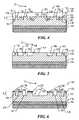
- a substrate 10patterned in accordance with the present invention, is shown having surface undulations 12 and surface polygonal structures 14 . It is problematic to pattern substrate 10 with features having dimensions on the order of the dimensions of undulations 12 and polygonal structures 14 , because the substrate 10 presents a non-planar, i.e., roughened topology, to the pattern process. As a result, undulations 12 and polygonal structures 14 , commonly referred to as planarity perturbations, make difficult controlling feature dimensions of patterns formed on substrate 10 .
- planarity perturbationsmake difficult controlling feature dimensions of patterns formed on substrate 10 .
- One of the advantages of the present inventionis reducing, if not abrogating, problematic effects of planarity perturbations employing a multi-layer film stack 16 to pattern the substrate underlying the surface.
- Multi-layer film stack 16includes a primer layer 18 deposited on a surface 20 of substrate 10 , a patterned layer 22 disposed upon primer layer 18 , and an etch-differential layer 24 deposited upon patterned layer 22 .
- Primer layer 18functions to provide surface 26 with planarity perturbations having a frequency that is less than the frequency of the planarity perturbations in surface 20 .
- Patterned layer 22 and etch-differential layer 24define an etch rate differential interface 28 that results from the relative etch rates and thicknesses of the materials from which patterned layer 22 and etch-differential layer 24 are formed. This facilitates formation, on substrate 10 , of a pattern corresponding to a shape of patterned layer 22 .
- patterned layer 22is provided with features that include projections 30 having a thickness t 1 , and recessions 32 having a thickness t 2 , measured between primer layer 18 and a bottom of recessions 32 .
- Thickness t 2is shown varying over the area of patterned layer 22 to the planarity perturbations that presents as curved surface 26 in primer layer 18 . Thickness t 2 is referred to as a residual thickness. Thicknesses “t 1 ” and “t 2 ” may be any thickness desired, dependent upon the application.
- each of projections 30has an apex surface 34 and each of recessions 32 has a nadir surface 36 .
- the thickness differential between t 1 and t 2 of projections 30 and recessions 32defines the amount of etch time required before exposing regions of substrate 10 .
- some or all of patterned layer 22is sacrificed during the etching process to provide the desired dimensions of the pattern eventually recorded in substrate 10 . Assuming a uniform thickness t 2 , a greater amount of etch time is required to expose regions of substrate 10 in superimposition with projections 30 compared with the time required for regions of substrate 10 in superimposition with recessions 32 .
- etchingwill commence sooner in regions of substrate 10 in superimposition with recessions 32 than regions in superimposition with projections 30 . This facilitates formation of a pattern in substrate 10 corresponding to the shape of patterned layer 22 .
- the relational dimensions between the differing features of the patternreferred to as etched pattern characteristics (EPC), eventually transferred onto substrate 10 , i.e., the recorded pattern, may be controlled as desired.
- EPCetched pattern characteristics
- planarity perturbationsmay result in exposure of some regions of substrate 10 in superimposition with projections 34 before exposure of regions of substrate 10 in superimposition with recessions 32 . As a result features of the pattern may be lost, which is undesirable.
- Etch-differential layer 24provides added variability in a given pattern transfer process for a given patterned layer by modifying the EPC. This facilitates overcoming problems associated with the planarity perturbations. Specifically, for a given etch process and patterned layer 22 , etch-differential layer 24 operates to modify the EPC by varying the time required before the etch chemistry breakthrough of all, or any sub-portion of, the patterned layer 22 to expose the region of substrate 10 in superimposition therewith.
- the modification of the EPCis dependent upon several factors.
- One of these factorsincludes the relative etch rates of the materials from which patterned layer 22 and etch-differential layer 24 are formed.
- Another factoris the variation in the spacing between normalization surface 40 and an interface of patterned layer 22 with etch-differential layer 24 , with the interface being referred to as etch rate interface (ERI) over the area of the ERI.
- ERIetch rate interface
- the variations in distance between normalization surface 40 and the ERIare a function of the shape of the relative shapes of both normalization surface 40 and patterned layer 22 . It is the volume of etch-differential layer 24 disposed between normalization surface 40 and the ERI that defines an etch-differential interface.
- etch differential interface 28provides the modification to the EPC.
- the planarity perturbationsinclude undulations 12 and polygonal structures 14 ; however, it should be understood that the topology of surface 20 may include any known shape, including substantially smooth, if not planar regions over a substantial area thereof. Further, the entire surface 20 may comprise undulations 12 , or the entire surface 20 may comprise polygonal structures 14 . Further, surface 20 may be comprised of silicon and any native oxide present thereon that is associated with a standard silicon wafer or may include an indium phosphate wafer, a gallium arsenide wafer, a gallium nitride wafer and the like. Furthermore, substrate 10 may include any one of the aforementioned wafers with one or more pre-existing layers deposited thereon, any one of which may be comprised of a metallic material, a dielectric material or combination thereof.
- Primer layer 18is applied to substrate 10 employing any known technique, e.g., chemical vapor deposition techniques, atomic layer deposition techniques, physical vapor deposition techniques, spin-coating techniques, imprint lithography techniques and the like.
- primer layer 18may be formed from a material available from Brewer Science, Inc. of Rolla Mo. under the trade name DUV30J-6 that is spun-on substrate 10 .
- Primer layer 18is typically provided with a thickness to function as an anti-reflective coating and provide a continuous, smooth, relatively defect-free surface that may exhibit excellent adhesion to material deposited thereon and without being opaque to optical sensing equipment employed to detect patterns, such as alignment marks (not shown), on substrate 10 .
- Both patterned layer 22 and etch-differential layer 24are deposited using any known technique, e.g., chemical vapor deposition techniques, atomic layer deposition techniques, physical vapor deposition techniques, spin-coating techniques, imprint lithography techniques and the like.
- patterned layer 22 and etch-differential layer 24are formed employing imprint lithography techniques.
- An exemplary technique for forming patterned layer 22employs depositing a plurality of droplets of imprinting material, referred to as a drop-dispense technique.
- An exemplary drop dispense techniqueis described in U.S.
- Patterned layer 22includes the features discussed above.
- Etch-differential layer 24includes first and second opposed sides. The first side faces patterned layer 22 and has a profile complementary to the profile of the patterned layer 22 . The second side faces away from patterned layer 22 forming a substantially smooth if not planar surface, defining a normalization surface 40 .
- patterned layer 22is a polymerized and cross-linked silicon-free material formed from the following composition:
- the acrylate component isobornyl acrylate (IBOA)has the following structure:
- n-hexyl acrylatehas the following structure:
- nHAis employed to provide the desired viscosity of COMPOSITION 1, in the liquid phase, to be in a range 2-9 Centipoises. Another advantage of nHA is that it improves the flexibility of COMPOSITION 1.
- An exemplary sample of nHAis available from Sigma-Aldrich of St. Louis, Mo. under product number 408905.
- a cross-linking component, ethylene glycol diacrylatehas the following structure:
- EGDAfacilitates cross-linking of nHA and IBOA during polymerization of COMPOSITION 1, as well as contributes to the modulus and stiffness build up.
- An initiator component, 2-hydroxy-2-methyl-1-phenyl-propan-1-oneis available from Ciba Specialty Chemicals of Tarrytown, N.Y. under the trade name DAROCUR 1173, has the following structure:
- the initiatoris responsive to a broad band of ultra-violet radiation to facilitate cross-linking and polymerization of the components of COMPOSITION 1.
- the component R 1 R 2is a surfactant having the general structure R 1 ⁇ F(CF 2 CF 2 ) y , with y being in a range of 1 to 7, inclusive, and R 2 ⁇ CH 2 CH 2 O(CH 2 CH 2 O) x H, with X is in a range of 0 to 15, inclusive.
- the surfactantmay be any known in the art that provides COMPOSITION 1 with suitable wetting properties in the liquid phase, as well as desired release characteristics in the solid phase.
- a surfactantis defined as any molecule, one tail of which is hydrophobic.
- Surfactantsmay be either fluorine-containing, e.g., include a fluorine chain, or may not include any fluorine in the surfactant molecule structure.
- An exemplary surfactanthas the following general structure:
- etch differential layer 24is formed employing the drop-dispense technique discussed above with respect to patterned layer 22 .
- a plurality of droplets (not shown) of imprinting materialare deposited atop of patterned layer 22 and a planarization mold (not shown) is placed in contact therewith.
- COMPOSITION 2differs from COMPOSITION 1 by the substitution of nHA with acryloxymethylpentamethyldisiloxane that has the following structure:
- COMPOSITION 2The remaining components of COMPOSITION 2 are that same as COMPOSITION 1, but are present in differing amounts.
- IBOA of COMPOSITION 2typically comprises approximately 37% of COMPOSITION 2, and EGDA and 2-hydroxy-2-methyl-1-phenyl-propan-1-one, comprising approximately 18% and 3%, respectively.
- the surfactant R 1 R 2is approximately 0.5% of the COMPOSITION.
- Composition 3differs from COMPOSITION 2 only by the substitution of acryloxymethylpentamethyldisiloxane with acryloxymethylbis(trimethylsiloxy)methylsilane.
- the component acryloxymethylbis(trimethylsiloxy)methylsilanehas the following structure:
- etch-differential layer 24after formation of etch-differential layer 24 , a blanket etch using, for example, an RIE process with a halogen gas mixture of approximately 70% CF4 and 30% O 2 , is employed to remove portions of etch-differential layer 24 substantially uniformly over a volume thereof to provide a crown surface 44 .
- Other gas mixtures that may be includedcontain CHF3, SF6 and other fluorinated chemistries know to one of ordinary skill in the etching art.
- An exemplary etch chemistryis discussed by Johnson et al. in ADVANCES IN STEP AND FLASH IMPRINT LITHOGRAPHY, in a white paper distributed at the SPIE Microlithography Conference held in Santa Clara, Calif. from Feb.
- Crown surface 44is defined by exposing the apex surface 34 of the projections 30 .
- adjacent apex surfaces 34are separated by regions 46 of etch-differential layer 24 remaining after formation of crown surface 44 .
- crown surface 44is subjected to an anisotropic etch.
- the etch chemistry of the anisotropic etchis selected to take advantage of the etch-differential provided by crown surface 44 by maximizing etching of projections 30 and segments of patterned layer 22 in superimposition therewith, while minimizing etching of regions 46 in superimposition with recessions 32 .
- advantagewas taken of the distinction of the silicon content between the patterned layer 22 and etch-differential layer 24 .
- an RIE etch with an oxygen-based chemistryit was determined that an in-situ hardened mask 48 would be created in the regions 46 proximate to the surface thereof.
- etch processessuch as the types discussed above may be employed to transfer a pattern onto substrate 10 corresponding to the recorded pattern.
- the recorded patternmay be covered with a conductive material (not shown), such as aluminum, copper, tungsten, titanium, ti-tungsten or a combination thereof and the like, to, inter alia, fill recesses in furtherance of contact formation, discussed more fully below.
- An advantage with the present inventionis that control over the dimensions of the features is facilitated despite the presence of planarity perturbations on substrate 10 .
- normalization surface 40is provided with a profile to ensure that the maximum difference between any two of distances k 2 , k 4 , k 6 , k 8 , k 10 and k 12 is less than 1 ⁇ 2 the height of the smallest projection 30 .
- Control of variations between distances, k 1 , k 3 , k 5 , k 7 , k 9 and k 11is not as critical so along as the measure of any one of distances k 1 , k 3 , k 5 , k 7 , k 9 and k 11 is no less than the measure of the largest distance among distances k 2 , k 4 , k 6 , k 8 , k 10 and k 12 .
- the distortions occurring during formation of recorded patternis substantially independent of the planarity perturbations, by decoupling the resolution of the patterning process from the resulting variations in the thickness t 2 over the area of patterned layer 22 .
- the resolution of the patterning processmay be substantially decoupled from the thickness t 2 , in addition to the variations in the same.
- the aspect ratio of the recorded patternwas defined, in part, by the difference between t 2 and. t 1 .
- t 2being on the order of the size of t 1 , or larger than t 1 , would result in no features being produced in the recorded pattern.
- control over thickness t 2becomes problematic, because the same varies over the area of patterned layer 22 . This may also result in a loss of pattern features.
- the time required to imprint increased as the feature dimensions on the templatedecreased, particularly with low viscosity imprinting materials, e.g., having a viscosity of less than 25 Centipoises, wherein the patterning process is dominated by the capillary forces of the imprinting material with the template (not shown).
- compressive forcesmay be applied to reduce the time required to fill the features of the template (not shown)
- the mechanical strength of substrate 10becomes a limitation when patterning materials having high viscosity, e.g., in a range of 25 to 10,000 Centipoises. At the greater range of viscosity the patterning process becomes dominated by viscous forces of the imprinting material, as opposed to capillary forces.
- the compressive force required to pattern an imprinting materialis believed to increase cubically as thickness t 2 decreases.
- variations in the thickness t 2may be modified without unduly deteriorating the resolution of the features to be formed in the recorded pattern.
- the difference between t 2max and t 2minmay be the same size or greater than t 1 .
- thickness t 2may be the same size as thickness t 1 , or may be two to ten times greater than t 1 .
- An advantage with substantially increasing the thickness t 2is that the compressive forces required to achieve an imprint process may be substantailly independent of thickness t 2 , which facilitates the patterning process dominated by visous forces. Further, increasing thickness t 2 facilitates reversing the tone of the pattern formed in the substrate so that the tone may be commensurste with the tone of the pattern of patterned layer 22 .
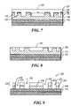
- a substrate 110including a primer layer 118 , a patterned layer 122 and an etch-differential layer 124 disposed thereon, which correspond to primer layer 18 , patterned layer 22 and etch-differential layer 24 , respectively.
- Patterned layer 122includes a plurality of projections 130 and recessions 132 that are analogous to projections 30 and recession 32 .
- Projections 130extend from a nadir surface 133 , a distance h 1 , terminating in an apex surface 134 .
- a normalization surface 140defined by etch differential layer 124 , is spaced-apart from projections 130 in a manner discussed above with respect to normalization surface 40 and projections 30 .
- etch differential layer 124is subjected to a blanket etch to form conformal surface 144 in a manner discussed above with respect to forming conformal surface 44 .
- conformal surface 144is defined by exposed apex surface 134 separated by regions 146 of etch differential layer 124 .
- an RIE process with oxygen based chemistryis employed to remove projections 130 and the portions of patterned layer 122 in superimposition therewith to expose regions 150 of patterned layer 122 , forming projections 135 , spaced apart by recessions 137 .
- Projections 135include a hard mask 148 of the material from which etch-differential layer 124 is formed. Regions 150 may be closer, further or the same distance from substrate 110 than nadir surfaces 133 , dependent upon the application. A height, h 2 , of projections 135 is defined as a function of the distance regions 150 are from substrate 110 .
- regions 150are closer to substrate 110 than nadir surface 133 and provide projections 135 with a height equal to distance h 1 . Further, projections 135 are shifted in phase along the x-direction with respect to projections 130 . Particularly, projections 135 are in superimposition with the same regions of substrate 110 with which recessions 132 are in superimposition. Moreover, the dimensions of projections 135 are defined by regions 146 .
- a second etch-differential layer 224is deposited over projection 135 , filling recessions 137 .
- Etch-differential layer 224is formed from the material as discussed with respect to etch differential layer 124 .
- Etch differential layer 224has a normalization surface 240 configured in the manner discussed with respect to normalization surface 240 .
- a crown surface 244is generated in a manner discussed above with respect to crown surface 144 . This is followed by removal of projections 135 .
- the resultis that a pattern 239 , having a plurality of projections 230 and recessions 232 , is generated on substrate 110 that has the same tone as the pattern in the patterned layer 122 , i.e., one may invert the pattern obtained by the process discussed with respect to FIGS. 1-3 .
- pattern 239is shifted in phase along the X-direction with respect to pattern 139 , with the understanding that pattern 239 may shift in phase along the Y-direction, which is into the page of FIGS. 1-3 .
- pattern 239is shifted in phase in a direction so that projections 230 are in superimposition with the same regions of substrate 110 with which projections 130 are in superimposition.
- Pattern 139is said to be shifted 180° out of phase along the X and Y-directions with respect to pattern 239 .
- the remaining portions of etch differential layer 224may be removed.
- the features of the patternmay be greater than, less than or equal to the dimensions of the features in the patterned layer 122 .
- tone reversalis found when fabricating patterned layer 22 employing imprint lithography techniques. It has been found that filling of features on a template (not shown), such as recesses, may be difficult if the same are too small. With the tone reversal process, the recess may be fabricated in the template (not shown) as protrusions with the same being subsequently formed into a recorded pattern as recessions. In other words, the tone of the pattern in the template may be chosen independent of the recorded tone of the recorded pattern desired. Instead, the tone of the pattern in the template may be selected to satisfy other operational characteristics of the imprint process, e.g., throughput by decreasing feature fill-time.
- patterned layer 322is shown having a plurality of features formed on substrate 310 , which include projections 330 having a thickness t 3 , shoulders 331 having a thickness t 4 and sub-portions 332 having a thickness t 5 .
- Projection 330 and shoulders 331define a bi-level projection on the surface of substrate 310 .
- Thickness t 5is referred to as a residual thickness. Thicknesses “t 3 ”, “t 4 ” and “t 5 ” may be any thickness desired, dependent upon the application.
- patterned layer 322is transferred onto substrate 310 to form a via portion (not shown) and a trench portion (not shown) therein, discussed more fully below.
- substrate 310may include several pre-existing layers disposed upon a wafer 312 , shown as layers 314 , 315 separated by etch stop layers 316 , 317 and 318 .
- Etch-differential layer 324is disposed adjacent to patterned layer 322 .
- Substrate 310 , patterned layer 322 and etch-differential layer 324define a multi-layered structure 338 .
- a blanket etchis employed to remove portions of etch-differential layer 324 to provide multi-layered 338 structure with the crown surface 344 .
- Crown surface 344is defined by an exposed apex surface 334 of each projection 330 and regions 346 that remain of etch-differential layer 324 after the blanket etch.
- crown surface 344is subjected to an anisotropic etch.
- the etch chemistry of the anisotropic etchis selected to maximize etching of projections 330 and the segments of patterned layer 322 in superimposition therewith, while minimizing etching of the regions 346 .
- advantagewas taken of the distinction of the silicon content between the patterned layer 322 and regions 346 to expose regions 350 of substrate 310 , as discussed above with respect to regions 46 and patterned layer 22 with respect to FIGS. 2 and 3 .
- etch processesincluding the processes discussed above, are employed to remove regions 346 and portions of multi-layered structure 338 in superimposition with regions 346 to expose regions 354 and 356 .
- Regions 354 and 356define a trench portion 358 and a via portion 360 .
- a subsequent etch process or lift-off processis employed to remove remaining portions of layers 322 and 324 .
- via portion 360 and trench portion 358may be concurrently filled with a conductive material, such as aluminum, copper, tungsten, titanium, ti-tungsten or a combination thereof and the like, to form a contact 362 and a conductive line 364 , shown in FIG. 15 .
- the advantages of this processare manifold.
- self-aligned vias and trenchesmay be formed in substrate 310 while precisely controlling the dimensions thereof. This reduces transfer distortions that may be attributable to planarity perturbations.
- etch-differential 24 layermay be formed employing spin-on techniques as discussed in U.S. patent application Ser. No. 10/789,319 filed Feb. 27, 2004 entitled COMPOSITION FOR AN ETCHING MASK COMPRISING A SILICON-CONTAINING MATERIAL.
- spin-on techniquesdiscussed in U.S. patent application Ser. No. 10/789,319 filed Feb. 27, 2004 entitled COMPOSITION FOR AN ETCHING MASK COMPRISING A SILICON-CONTAINING MATERIAL.
- hydroxyl-functional polysiloxanecomprises approximately 4% of the composition
- hexamethoxymethylmelaminecomprises approximately 0.95%
- toluenesulfonic acidcomprises approximately 0.05%
- methyl amyl ketonecomprises approximately 95%.
- hydroxyl-functional polysiloxanecomprises approximately 4% of the composition
- hexamethoxymethylmelaminecomprises approximately 0.7%
- gamma-glycidoxypropyltrimethoxysilanecomprises approximately 0.25%
- toluenesulfonic acidcomprises approximately 0.05%
- methyl amyl ketonecomprises approximately 95%.
- Both COMPOSITIONS 4 and 5are made up of at least 4% of the silicone resin.
- the quantity of silicon present in etch-differential layers 24 , 124 , 224 and 324is at least 10% by weight and typically in a range of 20% or greater.
- the quantity and composition of the solvent present in COMPOSITIONS 4 and 5is selected so that a substantial portion of the solvent evaporates during spin-coating application of the COMPOSITIONS 4 or 5 on patterned layers 22 , 122 and 322 .
- approximately 90% of the solventevaporates during spin-coating.
- the remaining 10% of the solventevaporates, leaving etch-differential layer 24 , 124 , 224 and 324 with approximately 20% silicon by weight.
- An exemplary method of forming etch-differential layers 24 , 124 , 224 and 324includes spinning-on approximately 4 mL of the silicon-containing material deposited proximate to a center of the previously deposited layer. To that end, substrates 10 , 110 or 310 are spun at 1000 rev/min for 1 minute by placing substrate 10 , 110 or 310 on a hot plate. Thereafter, the silicon-containing material is subjected to thermal energy by baking at 150° C. for 1 min. This produces the silicon-containing material from which etch-differential layer 24 , 124 , 224 and 324 is formed, with thickness variations of 20 nm or less.
- the aforementioned spin-coating and curing processesare simply repeated.
- the solvent employedis selected so as not to remove, “wash away,” silicon-containing material in a well-cured etch-differential layer.
- patterned layers 22 , 122 and 322from a modified composition consisting of a mixture of COMPOSITIONS 1 and 2, when used in conjunction with etch differential layers 24 , 124 , 224 and 324 , respectively, formed from one of COMPOSITIONs 4 and 5, provided superior control over the anisotropy of the recessions in the recorded pattern.
- the modified compositionprovides layers 22 , 122 and 322 with approximately 2-6% of silicon by weight.
- an exemplary modified compositionconsists of 20-70% of COMPOSITION 2, with the remainder consisting of COMPOSITION 1.
- Thisprovides a silicon content differential between one of patterned layers 22 , 122 and 322 and one of etch differential layers, 24 , 124 , 224 and 324 .
- patterned layers 22 , 133 and 322with low concentrations of silicon, bowing of recessions, e.g., recessions 32 , 132 and 137 and 232 , was reduced, if not avoided.
- Further control over formation of the aforementioned recessionswas achieved by cooling substrates 10 , 110 and 310 to approximately zero degrees Celsius, as well as by employing reducing chemistries in lieu of the aforementioned oxidizing chemistries during etching.
- Exemplary reducing chemistriesinclude H 2 /N 2 , CO/N 2 , CH 4 /N 2 and the like.
- the aforementioned processesmay be altered to take advantage of the material of the layer upon which pattern occurs.
- patterned layers 22 , 122 and 322from COMPOSITIONS 2, 4 or 5, with etch-differential layers 24 , 124 , 224 and 324 being formed from COMPOSITION 1.
- primer layer 18from one of COMPOSITIONS 2-5, i.e., were the surface upon which primer layer 18 disposed formed from a non-silicon containing organic material.
- primer layer 18from COMPOSITION 1.
- the etch process employedwould be established to provide the desired etch selectivity in the manner similar to that described above.
- patterned layer 422is deposited on substrate 410 employing any known deposition method.
- patterned layer 422is formed from COMPOSITION 1 employing imprint lithography generated by a plurality of spaced-apart projections 430 and recessions 432 .
- a nadir portion 436 of recessions 432has a residual thickness t 6 .
- patterned layer 422is subjected to an etch process, such as an RIE oxygen etch discussed above, to remove nadir portions 436 .
- an etch processsuch as an RIE oxygen etch discussed above.
- pattern 433is formed on substrate 410 .
- a deleterious effect that occurs during removing of nadir portions 436is that an apex surface 434 of each of projections 430 assumes a faceted shape.
- a conductive materialis deposited to cover pattern 433 , including apex surfaces 434 , forming a conductive layer 424 having a conforming side, conforming to a shape of pattern 433 and normalization side 440 disposed opposite to the conforming side. Normalization side 440 is spaced-apart from projections 430 .
- An exemplary conductive materialis copper, but may include any of the conductive materials mentioned above.
- a suitable processmay include a chemical mechanical polishing/planarization (CMP) process forming, were conductive layer 424 formed from metal, or blanket etch were a conductive layer 424 formed from a conductive polymer.
- CMPchemical mechanical polishing/planarization
- a CMP processis employed to achieve formation of a substantially smooth, if not planar, crown surface 444 .
- the CMP processis selected based upon the material from which patterned layer 422 and conductive layer 424 are formed so that apex surfaces 434 are exposed in normalization surface having a substantially planar profile. Specifically, the faceted shape of apex surfaces is removed while providing crown surface 444 with a substantially smooth if not planar profile.
- multi-layer structure 438is subjected to an RIE process and oxygen-based chemistry, as discussed above.
- the etch processremoves projection 430 , leaving a plurality of spaced-apart metal lines 450 .
- metal lines 550may be employed to form metal lines 550 with stepped shapes, e.g., a pair of spaced-apart shoulders 552 disposed between an apex surface 530 and substrate 510 , shown in FIG. 21 .
- projections 430may be covered with a non-conductive material, e.g., a dielectric material, to form dielectric layer 624 .
- a non-conductive materiale.g., a dielectric material
- Exemplary dielectric materials included, of dielectric materials applicable for this purpose,are silsesquioxanes and metbyl-silsesquioxanes, spin-on glass that are applied employing conventional deposition techniques.
- Dielectric layer 624covers pattern 433 , including apex surfaces 434 .
- dielectric layer 624includes a conforming side, conforming to a shape of pattern 433 and normalization side 640 disposed opposite to the conforming side. Normalization side 640 is spaced-apart from projections 630 .
- normalization side 640is subjected to a blanket etch, such as a CF 4 /O 2 plasma or CHF 3 /O 2 plasma etch, to expose apex surfaces 434 of projections 430 , forming a multi-layer structure 638 having a crown surface 644 .
- Crown surface 644is formed to be substantially smooth, if not, planar.
- multi-layer structure 638is subjected to an etch process that includes RIE with an oxygen plasma chemistry as discussed above.
- the etch processremoves projections 430 , leaving a plurality of spaced-apart dielectric pillars 650 . It should be understood that the same process may be employed to form dielectric pillars with stepped shapes, as discussed above.
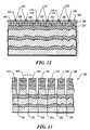
- a multi-layered structure 700is shown having a substrate 702 , a primer layer 704 , a patterned layer 706 and an etch-differential layer 708 .
- Patterned layer 706includes projections 710 , with projections 710 being arcuate in shape.
- Multi-layered structure 700may be subjected to the process mentioned above with respect to FIGS. 4-9 , thus resulting in the formation of multi-layered structures 712 and 714 , shown in FIGS. 26 and 27 , respectively.
- the etching chemistryis such that a low etch selectivity is achieved between the patterned layer 706 and the etch-differential layer 708 .
- the etching chemistryis such that a high etch selectivity is achieved between the patterned layer 706 and the etch-differential layer 708 Further processes can be undertaken that would result in different patterns being etched into substrate 702 that might be useful for generating optical elements. Particularly, by tailoring the relative etch rates, and relative thicknesses of differential layer 708 , patterned layer 706 and primer layer 704 , the EPC may be modified so that the recorded pattern substantially differs from the pattern of the patterned layer 706 . It should be understood that the etch characteristics of primer layer 704 are similar to the etch characteristics of patterned layer 706 . Furthermore, primer layer 704 is optional and may be omitted, dependent upon the application.
Landscapes
- Physics & Mathematics (AREA)
- Geometry (AREA)
- Engineering & Computer Science (AREA)
- Manufacturing & Machinery (AREA)
- Microelectronics & Electronic Packaging (AREA)
- Shaping Of Tube Ends By Bending Or Straightening (AREA)
- Internal Circuitry In Semiconductor Integrated Circuit Devices (AREA)
- Laminated Bodies (AREA)
- Exposure Of Semiconductors, Excluding Electron Or Ion Beam Exposure (AREA)
Abstract
Description

and comprises approximately 55% of COMPOSITION 1 by weight, but may comprise 20-80% of the same. As a result, the mechanical properties of patterned layer22 are primarily attributable to IBOA. An exemplary sample of IBOA is available from Sigma-Aldrich of St. Louis, Mo. under product number 392103. The component n-hexyl acrylate (nHA) has the following structure:

and comprises approximately 27% of COMPOSITION 1 by weight, but may comprise 0 to 50% of the same. Also providing mechanical strength to patterned layer22, nHA is employed to provide the desired viscosity of COMPOSITION 1, in the liquid phase, to be in a range 2-9 Centipoises. Another advantage of nHA is that it improves the flexibility of COMPOSITION 1. An exemplary sample of nHA is available from Sigma-Aldrich of St. Louis, Mo. under product number 408905. A cross-linking component, ethylene glycol diacrylate, has the following structure:

and comprises approximately 15% of COMPOSITION 1 by weight, but may comprise 10-50% of the same. EGDA facilitates cross-linking of nHA and IBOA during polymerization of COMPOSITION 1, as well as contributes to the modulus and stiffness build up. An initiator component, 2-hydroxy-2-methyl-1-phenyl-propan-1-one is available from Ciba Specialty Chemicals of Tarrytown, N.Y. under the trade name DAROCUR 1173, has the following structure:

and comprises approximately 3% of COMPOSITION 1 by weight, but may comprise 0.1% to 5% of the same. The initiator is responsive to a broad band of ultra-violet radiation to facilitate cross-linking and polymerization of the components of COMPOSITION 1.

and is available under the trade name ZONYL® FSO-100 from DUPONT™, which consists of 0.25 to 2% of the composition, with the remaining components being reduced a proportionate amount.

The remaining components of COMPOSITION 2 are that same as COMPOSITION 1, but are present in differing amounts. For example, IBOA of COMPOSITION 2 typically comprises approximately 37% of COMPOSITION 2, and EGDA and 2-hydroxy-2-methyl-1-phenyl-propan-1-one, comprising approximately 18% and 3%, respectively. The surfactant R1R2is approximately 0.5% of the COMPOSITION.

The relative quantities of each of the components of COMPOSITION 3 are the same as discussed with COMPOSITION 2.
Claims (25)
Priority Applications (14)
| Application Number | Priority Date | Filing Date | Title |
|---|---|---|---|
| US10/946,565US7252777B2 (en) | 2004-09-21 | 2004-09-21 | Method of forming an in-situ recessed structure |
| PCT/US2005/032276WO2006033872A2 (en) | 2004-09-21 | 2005-09-12 | Method of forming an in-situ recessed structure |
| SG200807516-0ASG147418A1 (en) | 2004-09-21 | 2005-09-12 | Method of forming an in-situ recessed structure |
| SG200807515-2ASG147417A1 (en) | 2004-09-21 | 2005-09-12 | Method of forming an in-situ recessed structure |
| KR1020117030614AKR101262730B1 (en) | 2004-09-21 | 2005-09-12 | Method of forming an in-situ recessed structure |
| SG200807517-8ASG147419A1 (en) | 2004-09-21 | 2005-09-12 | Method of forming an in-situ recessed structure |
| EP09173395AEP2146369A3 (en) | 2004-09-21 | 2005-09-12 | Method of forming an in-situ recessed structure |
| JP2007532387AJP2008513229A (en) | 2004-09-21 | 2005-09-12 | In-situ insertion structure forming method |
| EP05796480AEP1794099A4 (en) | 2004-09-21 | 2005-09-12 | Method of forming an in-situ recessed structure |
| SG200807518-6ASG147420A1 (en) | 2004-09-21 | 2005-09-12 | Method of forming an in-situ recessed structure |
| KR1020077006500AKR101243646B1 (en) | 2004-09-21 | 2005-09-12 | Method of forming an in-situ recessed structure |
| EP09173416AEP2146370A3 (en) | 2004-09-21 | 2005-09-12 | Method of forming an in-situ recessed structure |
| TW094132084ATWI272649B (en) | 2004-09-21 | 2005-09-16 | Method of forming an in-situ recessed structure |
| JP2014042722AJP5848386B2 (en) | 2004-09-21 | 2014-03-05 | In-situ insertion structure forming method |
Applications Claiming Priority (1)
| Application Number | Priority Date | Filing Date | Title |
|---|---|---|---|
| US10/946,565US7252777B2 (en) | 2004-09-21 | 2004-09-21 | Method of forming an in-situ recessed structure |
Publications (2)
| Publication Number | Publication Date |
|---|---|
| US20060063277A1 US20060063277A1 (en) | 2006-03-23 |
| US7252777B2true US7252777B2 (en) | 2007-08-07 |
Family
ID=36074552
Family Applications (1)
| Application Number | Title | Priority Date | Filing Date |
|---|---|---|---|
| US10/946,565Active2026-03-29US7252777B2 (en) | 2004-09-21 | 2004-09-21 | Method of forming an in-situ recessed structure |
Country Status (2)
| Country | Link |
|---|---|
| US (1) | US7252777B2 (en) |
| TW (1) | TWI272649B (en) |
Cited By (7)
| Publication number | Priority date | Publication date | Assignee | Title |
|---|---|---|---|---|
| US20070243281A1 (en)* | 2006-04-18 | 2007-10-18 | Mitsuru Hasegawa | Method of Transcribing Fine Pattern and Fine Structure Pattern Transcription Apparatus |
| US20080118872A1 (en)* | 2003-03-25 | 2008-05-22 | Molecular Imprints, Inc. | Positive Tone Bi-Layer Method |
| US7547504B2 (en) | 2004-09-21 | 2009-06-16 | Molecular Imprints, Inc. | Pattern reversal employing thick residual layers |
| US20100120251A1 (en)* | 2008-11-13 | 2010-05-13 | Molecular Imprints, Inc. | Large Area Patterning of Nano-Sized Shapes |
| US20100237042A1 (en)* | 2009-03-23 | 2010-09-23 | Intevac, Inc. | Process for optimization of island to trench ratio in patterned media |
| US8828297B2 (en) | 2010-11-05 | 2014-09-09 | Molecular Imprints, Inc. | Patterning of non-convex shaped nanostructures |
| US9147687B2 (en) | 2013-10-02 | 2015-09-29 | Samsung Electronics Co., Ltd. | Methods of fabricating semiconductor devices |
Families Citing this family (2)
| Publication number | Priority date | Publication date | Assignee | Title |
|---|---|---|---|---|
| US7396475B2 (en) | 2003-04-25 | 2008-07-08 | Molecular Imprints, Inc. | Method of forming stepped structures employing imprint lithography |
| US8012394B2 (en)* | 2007-12-28 | 2011-09-06 | Molecular Imprints, Inc. | Template pattern density doubling |
Citations (82)
| Publication number | Priority date | Publication date | Assignee | Title |
|---|---|---|---|---|
| US4426247A (en) | 1982-04-12 | 1984-01-17 | Nippon Telegraph & Telephone Public Corporation | Method for forming micropattern |
| US4507331A (en) | 1983-12-12 | 1985-03-26 | International Business Machines Corporation | Dry process for forming positive tone micro patterns |
| US4512848A (en) | 1984-02-06 | 1985-04-23 | Exxon Research And Engineering Co. | Procedure for fabrication of microstructures over large areas using physical replication |
| US4657845A (en) | 1986-01-14 | 1987-04-14 | International Business Machines Corporation | Positive tone oxygen plasma developable photoresist |
| US4692205A (en) | 1986-01-31 | 1987-09-08 | International Business Machines Corporation | Silicon-containing polyimides as oxygen etch stop and dual dielectric coatings |
| US4731155A (en) | 1987-04-15 | 1988-03-15 | General Electric Company | Process for forming a lithographic mask |
| JPH0224848A (en) | 1988-07-14 | 1990-01-26 | Canon Inc | Production of substrate for optical recording medium |
| JPH0292603A (en) | 1988-09-30 | 1990-04-03 | Hoya Corp | Manufacture of data recording board with guide groove |
| US4931351A (en) | 1987-01-12 | 1990-06-05 | Eastman Kodak Company | Bilayer lithographic process |
| US4959252A (en) | 1986-09-29 | 1990-09-25 | Rhone-Poulenc Chimie | Highly oriented thermotropic optical disc member |
| US4976818A (en) | 1987-10-26 | 1990-12-11 | Matsushita Electric Industrial Co., Ltd. | Fine pattern forming method |
| US5028366A (en) | 1988-01-12 | 1991-07-02 | Air Products And Chemicals, Inc. | Water based mold release compositions for making molded polyurethane foam |
| US5071694A (en) | 1989-02-21 | 1991-12-10 | Kanegafuchi Kagaku Kogyo Kabushiki Kaisha | Multi-layer resist |
| US5173393A (en) | 1989-04-24 | 1992-12-22 | Siemens Aktiengesellschaft | Etch-resistant deep ultraviolet resist process having an aromatic treating step after development |
| US5198326A (en) | 1990-05-24 | 1993-03-30 | Matsushita Electric Industrial Co., Ltd. | Process for forming fine pattern |
| US5234793A (en) | 1989-04-24 | 1993-08-10 | Siemens Aktiengesellschaft | Method for dimensionally accurate structure transfer in bilayer technique wherein a treating step with a bulging agent is employed after development |
| US5240550A (en) | 1990-09-21 | 1993-08-31 | U.S. Philips Corp. | Method of forming at least one groove in a substrate layer |
| US5314772A (en) | 1990-10-09 | 1994-05-24 | Arizona Board Of Regents | High resolution, multi-layer resist for microlithography and method therefor |
| US5425848A (en) | 1993-03-16 | 1995-06-20 | U.S. Philips Corporation | Method of providing a patterned relief of cured photoresist on a flat substrate surface and device for carrying out such a method |
| US5434107A (en) | 1994-01-28 | 1995-07-18 | Texas Instruments Incorporated | Method for planarization |
| US5480047A (en) | 1993-06-04 | 1996-01-02 | Sharp Kabushiki Kaisha | Method for forming a fine resist pattern |
| US5545367A (en) | 1992-04-15 | 1996-08-13 | Soane Technologies, Inc. | Rapid prototype three dimensional stereolithography |
| US5601641A (en) | 1992-07-21 | 1997-02-11 | Tse Industries, Inc. | Mold release composition with polybutadiene and method of coating a mold core |
| US5700626A (en) | 1994-01-12 | 1997-12-23 | Lg Semicon Co., Ltd. | Method for forming multi-layer resist pattern |
| US5743998A (en) | 1995-04-19 | 1998-04-28 | Park Scientific Instruments | Process for transferring microminiature patterns using spin-on glass resist media |
| US5772905A (en) | 1995-11-15 | 1998-06-30 | Regents Of The University Of Minnesota | Nanoimprint lithography |
| US5849222A (en) | 1995-09-29 | 1998-12-15 | Johnson & Johnson Vision Products, Inc. | Method for reducing lens hole defects in production of contact lens blanks |
| US5849209A (en) | 1995-03-31 | 1998-12-15 | Johnson & Johnson Vision Products, Inc. | Mold material made with additives |
| WO1999005724A1 (en) | 1997-07-25 | 1999-02-04 | Regents Of The University Of Minnesota | Single-electron floating-gate mos memory |
| US5888650A (en) | 1996-06-03 | 1999-03-30 | Minnesota Mining And Manufacturing Company | Temperature-responsive adhesive article |
| US5907782A (en) | 1998-08-15 | 1999-05-25 | Acer Semiconductor Manufacturing Inc. | Method of forming a multiple fin-pillar capacitor for a high density dram cell |
| US6033977A (en) | 1997-06-30 | 2000-03-07 | Siemens Aktiengesellschaft | Dual damascene structure |
| US6046056A (en) | 1996-06-28 | 2000-04-04 | Caliper Technologies Corporation | High throughput screening assay systems in microscale fluidic devices |
| WO2000021689A1 (en) | 1998-10-09 | 2000-04-20 | The Trustees Of Princeton University | Microscale patterning and articles formed thereby |
| US6074827A (en) | 1996-07-30 | 2000-06-13 | Aclara Biosciences, Inc. | Microfluidic method for nucleic acid purification and processing |
| US6096655A (en) | 1998-09-02 | 2000-08-01 | International Business Machines, Corporation | Method for forming vias and trenches in an insulation layer for a dual-damascene multilevel interconnection structure |
| WO2001047003A2 (en) | 1999-12-23 | 2001-06-28 | University Of Massachusetts | Methods and apparatus for forming submicron patterns on films |
| US6309580B1 (en) | 1995-11-15 | 2001-10-30 | Regents Of The University Of Minnesota | Release surfaces, particularly for use in nanoimprint lithography |
| US6326627B1 (en) | 2000-08-02 | 2001-12-04 | Archimedes Technology Group, Inc. | Mass filtering sputtered ion source |
| US6329256B1 (en) | 1999-09-24 | 2001-12-11 | Advanced Micro Devices, Inc. | Self-aligned damascene gate formation with low gate resistance |
| US6334960B1 (en)* | 1999-03-11 | 2002-01-01 | Board Of Regents, The University Of Texas System | Step and flash imprint lithography |
| WO2002007199A1 (en) | 2000-07-18 | 2002-01-24 | Nanonex Corporation | Fluid pressure imprint lithography |
| US20020042027A1 (en) | 1998-10-09 | 2002-04-11 | Chou Stephen Y. | Microscale patterning and articles formed thereby |
| US6426288B1 (en) | 1996-08-28 | 2002-07-30 | Micron Technology, Inc. | Method for removing an upper layer of material from a semiconductor wafer |
| US6455411B1 (en) | 2000-09-11 | 2002-09-24 | Texas Instruments Incorporated | Defect and etch rate control in trench etch for dual damascene patterning of low-k dielectrics |
| WO2003010289A2 (en) | 2001-07-25 | 2003-02-06 | The Trustees Of Princeton University | Nanochannel arrays and their preparation and use for high throughput macromolecular analysis |
| US6518189B1 (en) | 1995-11-15 | 2003-02-11 | Regents Of The University Of Minnesota | Method and apparatus for high density nanostructures |
| US6517995B1 (en) | 1999-09-14 | 2003-02-11 | Massachusetts Institute Of Technology | Fabrication of finely featured devices by liquid embossing |
| US20030080471A1 (en) | 2001-10-29 | 2003-05-01 | Chou Stephen Y. | Lithographic method for molding pattern with nanoscale features |
| US6580172B2 (en) | 2001-03-02 | 2003-06-17 | Motorola, Inc. | Lithographic template and method of formation and use |
| WO2003079416A1 (en) | 2002-03-15 | 2003-09-25 | Princeton University | Laser assisted direct imprint lithography |
| US6646662B1 (en) | 1998-05-26 | 2003-11-11 | Seiko Epson Corporation | Patterning method, patterning apparatus, patterning template, and method for manufacturing the patterning template |
| WO2003099536A1 (en) | 2002-05-24 | 2003-12-04 | Chou Stephen Y | Methods and apparatus of field-induced pressure imprint lithography |
| US20040007799A1 (en) | 2002-07-11 | 2004-01-15 | Choi Byung Jin | Formation of discontinuous films during an imprint lithography process |
| US20040008334A1 (en) | 2002-07-11 | 2004-01-15 | Sreenivasan Sidlgata V. | Step and repeat imprint lithography systems |
| US20040009673A1 (en) | 2002-07-11 | 2004-01-15 | Sreenivasan Sidlgata V. | Method and system for imprint lithography using an electric field |
| US20040022888A1 (en) | 2002-08-01 | 2004-02-05 | Sreenivasan Sidlgata V. | Alignment systems for imprint lithography |
| US20040021866A1 (en) | 2002-08-01 | 2004-02-05 | Watts Michael P.C. | Scatterometry alignment for imprint lithography |
| US20040021254A1 (en) | 2002-08-01 | 2004-02-05 | Sreenivasan Sidlgata V. | Alignment methods for imprint lithography |
| US20040029041A1 (en) | 2002-02-27 | 2004-02-12 | Brewer Science, Inc. | Novel planarization method for multi-layer lithography processing |
| US6696220B2 (en) | 2000-10-12 | 2004-02-24 | Board Of Regents, The University Of Texas System | Template for room temperature, low pressure micro-and nano-imprint lithography |
| US20040036201A1 (en) | 2000-07-18 | 2004-02-26 | Princeton University | Methods and apparatus of field-induced pressure imprint lithography |
| US6703190B2 (en) | 1999-12-07 | 2004-03-09 | Infineon Technologies Ag | Method for producing resist structures |
| US20040046288A1 (en) | 2000-07-18 | 2004-03-11 | Chou Stephen Y. | Laset assisted direct imprint lithography |
| US6716767B2 (en) | 2001-10-31 | 2004-04-06 | Brewer Science, Inc. | Contact planarization materials that generate no volatile byproducts or residue during curing |
| US6730256B1 (en) | 2000-08-04 | 2004-05-04 | Massachusetts Institute Of Technology | Stereolithographic patterning with interlayer surface modifications |
| US6737202B2 (en) | 2002-02-22 | 2004-05-18 | Motorola, Inc. | Method of fabricating a tiered structure using a multi-layered resist stack and use |
| US6743713B2 (en) | 2002-05-15 | 2004-06-01 | Institute Of Microelectronics | Method of forming dual damascene pattern using dual bottom anti-reflective coatings (BARC) |
| US20040110856A1 (en) | 2002-12-04 | 2004-06-10 | Young Jung Gun | Polymer solution for nanoimprint lithography to reduce imprint temperature and pressure |
| US20040124566A1 (en) | 2002-07-11 | 2004-07-01 | Sreenivasan Sidlgata V. | Step and repeat imprint lithography processes |
| US20040131718A1 (en) | 2000-07-18 | 2004-07-08 | Princeton University | Lithographic apparatus for fluid pressure imprint lithography |
| US20040137734A1 (en) | 1995-11-15 | 2004-07-15 | Princeton University | Compositions and processes for nanoimprinting |
| US6767983B1 (en) | 1999-03-30 | 2004-07-27 | Nippon Steel Chemical Co., Ltd. | Silicone resin and photosensitive resin composition containing the same |
| US6770852B1 (en) | 2003-02-27 | 2004-08-03 | Lam Research Corporation | Critical dimension variation compensation across a wafer by means of local wafer temperature control |
| US20040156108A1 (en) | 2001-10-29 | 2004-08-12 | Chou Stephen Y. | Articles comprising nanoscale patterns with reduced edge roughness and methods of making same |
| US6777170B1 (en) | 2000-08-04 | 2004-08-17 | Massachusetts Institute Of Technology | Stereolithographic patterning by variable dose light delivery |
| US6776094B1 (en) | 1993-10-04 | 2004-08-17 | President & Fellows Of Harvard College | Kit For Microcontact Printing |
| US20040192041A1 (en) | 2003-03-27 | 2004-09-30 | Jun-Ho Jeong | UV nanoimprint lithography process using elementwise embossed stamp and selectively additive pressurization |
| US20040188381A1 (en) | 2003-03-25 | 2004-09-30 | Molecular Imprints, Inc. | Positive tone bi-layer imprint lithography method |
| US20040211754A1 (en) | 2003-04-25 | 2004-10-28 | Molecular Imprints, Inc. | Method of forming stepped structures employing imprint lithography |
| US6814879B2 (en) | 2000-09-27 | 2004-11-09 | Kabushiki Kaisha Toshiba | Method for forming pattern |
| WO2004114016A2 (en) | 2003-06-09 | 2004-12-29 | Princeton University Office Of Technology Licensing And Intellectual Property | Imprint lithography with improved monitoring and control and apparatus therefor |
Family Cites Families (6)
| Publication number | Priority date | Publication date | Assignee | Title |
|---|---|---|---|---|
| US7186656B2 (en)* | 2004-05-21 | 2007-03-06 | Molecular Imprints, Inc. | Method of forming a recessed structure employing a reverse tone process |
| US20050253307A1 (en)* | 2004-05-11 | 2005-11-17 | Molecualr Imprints, Inc. | Method of patterning a conductive layer on a substrate |
| US7547504B2 (en)* | 2004-09-21 | 2009-06-16 | Molecular Imprints, Inc. | Pattern reversal employing thick residual layers |
| US7241395B2 (en)* | 2004-09-21 | 2007-07-10 | Molecular Imprints, Inc. | Reverse tone patterning on surfaces having planarity perturbations |
| US7041604B2 (en)* | 2004-09-21 | 2006-05-09 | Molecular Imprints, Inc. | Method of patterning surfaces while providing greater control of recess anisotropy |
| US7205244B2 (en)* | 2004-09-21 | 2007-04-17 | Molecular Imprints | Patterning substrates employing multi-film layers defining etch-differential interfaces |
- 2004
- 2004-09-21USUS10/946,565patent/US7252777B2/enactiveActive
- 2005
- 2005-09-16TWTW094132084Apatent/TWI272649B/enactive
Patent Citations (95)
| Publication number | Priority date | Publication date | Assignee | Title |
|---|---|---|---|---|
| US4426247A (en) | 1982-04-12 | 1984-01-17 | Nippon Telegraph & Telephone Public Corporation | Method for forming micropattern |
| US4507331A (en) | 1983-12-12 | 1985-03-26 | International Business Machines Corporation | Dry process for forming positive tone micro patterns |
| US4512848A (en) | 1984-02-06 | 1985-04-23 | Exxon Research And Engineering Co. | Procedure for fabrication of microstructures over large areas using physical replication |
| US4657845A (en) | 1986-01-14 | 1987-04-14 | International Business Machines Corporation | Positive tone oxygen plasma developable photoresist |
| US4692205A (en) | 1986-01-31 | 1987-09-08 | International Business Machines Corporation | Silicon-containing polyimides as oxygen etch stop and dual dielectric coatings |
| US4959252A (en) | 1986-09-29 | 1990-09-25 | Rhone-Poulenc Chimie | Highly oriented thermotropic optical disc member |
| US4931351A (en) | 1987-01-12 | 1990-06-05 | Eastman Kodak Company | Bilayer lithographic process |
| US4731155A (en) | 1987-04-15 | 1988-03-15 | General Electric Company | Process for forming a lithographic mask |
| US4976818A (en) | 1987-10-26 | 1990-12-11 | Matsushita Electric Industrial Co., Ltd. | Fine pattern forming method |
| US5028366A (en) | 1988-01-12 | 1991-07-02 | Air Products And Chemicals, Inc. | Water based mold release compositions for making molded polyurethane foam |
| JPH0224848A (en) | 1988-07-14 | 1990-01-26 | Canon Inc | Production of substrate for optical recording medium |
| JPH0292603A (en) | 1988-09-30 | 1990-04-03 | Hoya Corp | Manufacture of data recording board with guide groove |
| US5071694A (en) | 1989-02-21 | 1991-12-10 | Kanegafuchi Kagaku Kogyo Kabushiki Kaisha | Multi-layer resist |
| US5173393A (en) | 1989-04-24 | 1992-12-22 | Siemens Aktiengesellschaft | Etch-resistant deep ultraviolet resist process having an aromatic treating step after development |
| US5234793A (en) | 1989-04-24 | 1993-08-10 | Siemens Aktiengesellschaft | Method for dimensionally accurate structure transfer in bilayer technique wherein a treating step with a bulging agent is employed after development |
| US5198326A (en) | 1990-05-24 | 1993-03-30 | Matsushita Electric Industrial Co., Ltd. | Process for forming fine pattern |
| US5240550A (en) | 1990-09-21 | 1993-08-31 | U.S. Philips Corp. | Method of forming at least one groove in a substrate layer |
| US5314772A (en) | 1990-10-09 | 1994-05-24 | Arizona Board Of Regents | High resolution, multi-layer resist for microlithography and method therefor |
| US5545367A (en) | 1992-04-15 | 1996-08-13 | Soane Technologies, Inc. | Rapid prototype three dimensional stereolithography |
| US5601641A (en) | 1992-07-21 | 1997-02-11 | Tse Industries, Inc. | Mold release composition with polybutadiene and method of coating a mold core |
| US5425848A (en) | 1993-03-16 | 1995-06-20 | U.S. Philips Corporation | Method of providing a patterned relief of cured photoresist on a flat substrate surface and device for carrying out such a method |
| US5480047A (en) | 1993-06-04 | 1996-01-02 | Sharp Kabushiki Kaisha | Method for forming a fine resist pattern |
| US6776094B1 (en) | 1993-10-04 | 2004-08-17 | President & Fellows Of Harvard College | Kit For Microcontact Printing |
| US5700626A (en) | 1994-01-12 | 1997-12-23 | Lg Semicon Co., Ltd. | Method for forming multi-layer resist pattern |
| US5434107A (en) | 1994-01-28 | 1995-07-18 | Texas Instruments Incorporated | Method for planarization |
| US5849209A (en) | 1995-03-31 | 1998-12-15 | Johnson & Johnson Vision Products, Inc. | Mold material made with additives |
| US5743998A (en) | 1995-04-19 | 1998-04-28 | Park Scientific Instruments | Process for transferring microminiature patterns using spin-on glass resist media |
| US5849222A (en) | 1995-09-29 | 1998-12-15 | Johnson & Johnson Vision Products, Inc. | Method for reducing lens hole defects in production of contact lens blanks |
| US5772905A (en) | 1995-11-15 | 1998-06-30 | Regents Of The University Of Minnesota | Nanoimprint lithography |
| US20040137734A1 (en) | 1995-11-15 | 2004-07-15 | Princeton University | Compositions and processes for nanoimprinting |
| US6518189B1 (en) | 1995-11-15 | 2003-02-11 | Regents Of The University Of Minnesota | Method and apparatus for high density nanostructures |
| US6309580B1 (en) | 1995-11-15 | 2001-10-30 | Regents Of The University Of Minnesota | Release surfaces, particularly for use in nanoimprint lithography |
| US6809356B2 (en) | 1995-11-15 | 2004-10-26 | Regents Of The University Of Minnesota | Method and apparatus for high density nanostructures |
| US6828244B2 (en) | 1995-11-15 | 2004-12-07 | Regents Of The University Of Minnesota | Method and apparatus for high density nanostructures |
| US5888650A (en) | 1996-06-03 | 1999-03-30 | Minnesota Mining And Manufacturing Company | Temperature-responsive adhesive article |
| US6046056A (en) | 1996-06-28 | 2000-04-04 | Caliper Technologies Corporation | High throughput screening assay systems in microscale fluidic devices |
| US6074827A (en) | 1996-07-30 | 2000-06-13 | Aclara Biosciences, Inc. | Microfluidic method for nucleic acid purification and processing |
| US6426288B1 (en) | 1996-08-28 | 2002-07-30 | Micron Technology, Inc. | Method for removing an upper layer of material from a semiconductor wafer |
| US6033977A (en) | 1997-06-30 | 2000-03-07 | Siemens Aktiengesellschaft | Dual damascene structure |
| WO1999005724A1 (en) | 1997-07-25 | 1999-02-04 | Regents Of The University Of Minnesota | Single-electron floating-gate mos memory |
| US6646662B1 (en) | 1998-05-26 | 2003-11-11 | Seiko Epson Corporation | Patterning method, patterning apparatus, patterning template, and method for manufacturing the patterning template |
| US20030034329A1 (en) | 1998-06-30 | 2003-02-20 | Chou Stephen Y. | Lithographic method for molding pattern with nanoscale depth |
| US20020167117A1 (en) | 1998-06-30 | 2002-11-14 | Regents Of The University Of Minnesota | Release surfaces, particularly for use in nanoimprint lithography |
| US5907782A (en) | 1998-08-15 | 1999-05-25 | Acer Semiconductor Manufacturing Inc. | Method of forming a multiple fin-pillar capacitor for a high density dram cell |
| US6096655A (en) | 1998-09-02 | 2000-08-01 | International Business Machines, Corporation | Method for forming vias and trenches in an insulation layer for a dual-damascene multilevel interconnection structure |
| US20040118809A1 (en) | 1998-10-09 | 2004-06-24 | Chou Stephen Y. | Microscale patterning and articles formed thereby |
| US20020042027A1 (en) | 1998-10-09 | 2002-04-11 | Chou Stephen Y. | Microscale patterning and articles formed thereby |
| WO2000021689A1 (en) | 1998-10-09 | 2000-04-20 | The Trustees Of Princeton University | Microscale patterning and articles formed thereby |
| US6713238B1 (en) | 1998-10-09 | 2004-03-30 | Stephen Y. Chou | Microscale patterning and articles formed thereby |
| US6334960B1 (en)* | 1999-03-11 | 2002-01-01 | Board Of Regents, The University Of Texas System | Step and flash imprint lithography |
| US6719915B2 (en) | 1999-03-11 | 2004-04-13 | Board Of Regents, The University Of Texas System | Step and flash imprint lithography |
| US6767983B1 (en) | 1999-03-30 | 2004-07-27 | Nippon Steel Chemical Co., Ltd. | Silicone resin and photosensitive resin composition containing the same |
| US6517995B1 (en) | 1999-09-14 | 2003-02-11 | Massachusetts Institute Of Technology | Fabrication of finely featured devices by liquid embossing |
| US6329256B1 (en) | 1999-09-24 | 2001-12-11 | Advanced Micro Devices, Inc. | Self-aligned damascene gate formation with low gate resistance |
| US6703190B2 (en) | 1999-12-07 | 2004-03-09 | Infineon Technologies Ag | Method for producing resist structures |
| US6391217B2 (en) | 1999-12-23 | 2002-05-21 | University Of Massachusetts | Methods and apparatus for forming submicron patterns on films |
| WO2001047003A2 (en) | 1999-12-23 | 2001-06-28 | University Of Massachusetts | Methods and apparatus for forming submicron patterns on films |
| US20020132482A1 (en) | 2000-07-18 | 2002-09-19 | Chou Stephen Y. | Fluid pressure imprint lithography |
| US20040046288A1 (en) | 2000-07-18 | 2004-03-11 | Chou Stephen Y. | Laset assisted direct imprint lithography |
| WO2002007199A1 (en) | 2000-07-18 | 2002-01-24 | Nanonex Corporation | Fluid pressure imprint lithography |
| US6482742B1 (en) | 2000-07-18 | 2002-11-19 | Stephen Y. Chou | Fluid pressure imprint lithography |
| US20020177319A1 (en) | 2000-07-18 | 2002-11-28 | Chou Stephen Y. | Fluid pressure bonding |
| US20040131718A1 (en) | 2000-07-18 | 2004-07-08 | Princeton University | Lithographic apparatus for fluid pressure imprint lithography |
| US20040036201A1 (en) | 2000-07-18 | 2004-02-26 | Princeton University | Methods and apparatus of field-induced pressure imprint lithography |
| US6326627B1 (en) | 2000-08-02 | 2001-12-04 | Archimedes Technology Group, Inc. | Mass filtering sputtered ion source |
| US6777170B1 (en) | 2000-08-04 | 2004-08-17 | Massachusetts Institute Of Technology | Stereolithographic patterning by variable dose light delivery |
| US6730256B1 (en) | 2000-08-04 | 2004-05-04 | Massachusetts Institute Of Technology | Stereolithographic patterning with interlayer surface modifications |
| US6455411B1 (en) | 2000-09-11 | 2002-09-24 | Texas Instruments Incorporated | Defect and etch rate control in trench etch for dual damascene patterning of low-k dielectrics |
| US6814879B2 (en) | 2000-09-27 | 2004-11-09 | Kabushiki Kaisha Toshiba | Method for forming pattern |
| US6696220B2 (en) | 2000-10-12 | 2004-02-24 | Board Of Regents, The University Of Texas System | Template for room temperature, low pressure micro-and nano-imprint lithography |
| US6580172B2 (en) | 2001-03-02 | 2003-06-17 | Motorola, Inc. | Lithographic template and method of formation and use |
| WO2003010289A2 (en) | 2001-07-25 | 2003-02-06 | The Trustees Of Princeton University | Nanochannel arrays and their preparation and use for high throughput macromolecular analysis |
| US20040197843A1 (en) | 2001-07-25 | 2004-10-07 | Chou Stephen Y. | Nanochannel arrays and their preparation and use for high throughput macromolecular analysis |
| US20030080472A1 (en) | 2001-10-29 | 2003-05-01 | Chou Stephen Y. | Lithographic method with bonded release layer for molding small patterns |
| US20030080471A1 (en) | 2001-10-29 | 2003-05-01 | Chou Stephen Y. | Lithographic method for molding pattern with nanoscale features |
| US20040156108A1 (en) | 2001-10-29 | 2004-08-12 | Chou Stephen Y. | Articles comprising nanoscale patterns with reduced edge roughness and methods of making same |
| US6716767B2 (en) | 2001-10-31 | 2004-04-06 | Brewer Science, Inc. | Contact planarization materials that generate no volatile byproducts or residue during curing |
| US6737202B2 (en) | 2002-02-22 | 2004-05-18 | Motorola, Inc. | Method of fabricating a tiered structure using a multi-layered resist stack and use |
| US20040029041A1 (en) | 2002-02-27 | 2004-02-12 | Brewer Science, Inc. | Novel planarization method for multi-layer lithography processing |
| WO2003079416A1 (en) | 2002-03-15 | 2003-09-25 | Princeton University | Laser assisted direct imprint lithography |
| US6743713B2 (en) | 2002-05-15 | 2004-06-01 | Institute Of Microelectronics | Method of forming dual damascene pattern using dual bottom anti-reflective coatings (BARC) |
| WO2003099536A1 (en) | 2002-05-24 | 2003-12-04 | Chou Stephen Y | Methods and apparatus of field-induced pressure imprint lithography |
| US20040007799A1 (en) | 2002-07-11 | 2004-01-15 | Choi Byung Jin | Formation of discontinuous films during an imprint lithography process |
| US20040008334A1 (en) | 2002-07-11 | 2004-01-15 | Sreenivasan Sidlgata V. | Step and repeat imprint lithography systems |
| US20040009673A1 (en) | 2002-07-11 | 2004-01-15 | Sreenivasan Sidlgata V. | Method and system for imprint lithography using an electric field |
| US20040124566A1 (en) | 2002-07-11 | 2004-07-01 | Sreenivasan Sidlgata V. | Step and repeat imprint lithography processes |
| US20040021866A1 (en) | 2002-08-01 | 2004-02-05 | Watts Michael P.C. | Scatterometry alignment for imprint lithography |
| US20040022888A1 (en) | 2002-08-01 | 2004-02-05 | Sreenivasan Sidlgata V. | Alignment systems for imprint lithography |
| US20040021254A1 (en) | 2002-08-01 | 2004-02-05 | Sreenivasan Sidlgata V. | Alignment methods for imprint lithography |
| US20040110856A1 (en) | 2002-12-04 | 2004-06-10 | Young Jung Gun | Polymer solution for nanoimprint lithography to reduce imprint temperature and pressure |
| US6770852B1 (en) | 2003-02-27 | 2004-08-03 | Lam Research Corporation | Critical dimension variation compensation across a wafer by means of local wafer temperature control |
| US20040188381A1 (en) | 2003-03-25 | 2004-09-30 | Molecular Imprints, Inc. | Positive tone bi-layer imprint lithography method |
| US20040192041A1 (en) | 2003-03-27 | 2004-09-30 | Jun-Ho Jeong | UV nanoimprint lithography process using elementwise embossed stamp and selectively additive pressurization |
| US20040211754A1 (en) | 2003-04-25 | 2004-10-28 | Molecular Imprints, Inc. | Method of forming stepped structures employing imprint lithography |
| WO2004114016A2 (en) | 2003-06-09 | 2004-12-29 | Princeton University Office Of Technology Licensing And Intellectual Property | Imprint lithography with improved monitoring and control and apparatus therefor |
Non-Patent Citations (26)
| Title |
|---|
| Bailey et al., Step and Flash Imprint Lithography: Defect Analysis, Journal of Vacuum Science, B 19(6), pp. 2806-2810, Nov. 1, 2001. |
| Bailey et al., Step and Flash Imprint Lithography: Template Surface Treatment and Defect Analysis, Journal of Vacuum Science, B 18(6), pp. 3572-3577, Nov. 1, 2000. |
| Choi et al., Design of Orientation Stages for Step and Flash Imprint Lithography, Precision Engineering, pp. 192-199, Jan. 1, 2001. |
| Chou et al., Imprint Lithography with 25-Nanometer Resolution, Science vol. 272, pp. 85-87, Apr. 5, 1996. |
| Chou et al., Imprint Lithography with Sub-10 nm Feature Size and High Throughput, Microelectronic Engineering 35, pp. 237-240, Jan. 1, 1997. |
| Chou et al., Imprint of Sub-25 nm Vias and Trenches in Polymers, Appl. Phys. Lett. 67 (21), Nov. 20, 1995. |
| Chou et al., Lithogrpahically Induced Self-assembly of Periodic Polymer Micropillar Arrays, J. Vac. Sci. Technol. B 17 (6), pp. 3197-3202, Nov. 1, 1999. |
| Chou et al., Nanoimprint Lithography, Journal of Vacuum Science Technolgoy B 14(16), pp. 4129-4133, Nov. 1, 1996. |
| Chou et al., Ultrafest and Direct Imprint of Nanostructures in Silicon, Nature, Col. 417, (Jun. 2002), pp. 835-837, Jun. 1, 2002. |
| Chou, Nanoimprint Lithography and Lithographically Induced Self-Assembly, MRS Bulletin, pp. 512-517, Jul. 1, 2001. |
| Colburn et al., Characterization and Modeling of Volumetric and Mechanical Properties for Step and Flash Imprint Lithography Photopolymers, Journal of Vacuum Science Technology, vol. b. 19(6), Nov. 1, 2001. |
| Colburn et al., Development and Advantages of Step-and-Flash Lithography, Solid State Technology, Jul. 1, 2001. |
| Colburn et al., Step and Flash Imprint Lithography for Sub-100 nm Patterning, Proceedings of SPIE vol. 3997, pp. 453-457, Jan. 1, 2000. |
| Colburn et al., Step and Flash Imprint Lithography: A New Approach to High-Resolution Patterning, Proc. Of SPIE, vol. 3676, Mar. 1, 1999. |
| Haisma et al., Mold-assisted Nanolithography: A Process for Reliable Pattern Replication, J. Vac. Sci. Technol. B, pp. 4124-4128, Nov. 1, 1996. |
| Heidari, Nanoimprint Lithography at the 6 in. Wafer Scale, J. Vac. Sci. Technol. B 18(6), pp. 3557-3560, Nov. 1, 2000. |
| Johnson et al., Advances in Step and Flash Imprint Lithography, SPIE Microlithography Conference, Feb. 23, 2003. |
| Schneider et al., Stripes of Partially Fluorinated Alkyl Chains: Dipolar Langmuir Monolayers. |
| Translation of Japanese Patent 02-24848. |
| Translation of Japanese Patent 02-92603. |
| U.S. Appl. No. 10/843,194, filed May 11, 2004, Sreenivasan et al. |
| U.S. Appl. No. 10/946,159, filed Sep. 21, 2004, Miller et al. |
| U.S. Appl. No. 10/946,566, filed Sep. 21, 2004, Sreenivasan et. al. |
| U.S. Appl. No. 10/946,570, filed Sep. 21, 2004, Sreenivasan. |
| U.S. Appl. No. 10/946,574, filed Sep. 21, 2004, Choi et al. |
| U.S. Appl. No. 10/946,577, filed Sep. 21, 2004, Sreenivasan et al. |
Cited By (11)
| Publication number | Priority date | Publication date | Assignee | Title |
|---|---|---|---|---|
| US20080118872A1 (en)* | 2003-03-25 | 2008-05-22 | Molecular Imprints, Inc. | Positive Tone Bi-Layer Method |
| US7670953B2 (en) | 2003-03-25 | 2010-03-02 | Molecular Imprints, Inc. | Positive tone bi-layer method |
| US7547504B2 (en) | 2004-09-21 | 2009-06-16 | Molecular Imprints, Inc. | Pattern reversal employing thick residual layers |
| US20070243281A1 (en)* | 2006-04-18 | 2007-10-18 | Mitsuru Hasegawa | Method of Transcribing Fine Pattern and Fine Structure Pattern Transcription Apparatus |
| US8047835B2 (en)* | 2006-04-18 | 2011-11-01 | Hitachi High-Technologies Corporation | Method of transcribing fine pattern and fine structure pattern transcription apparatus |
| US20100120251A1 (en)* | 2008-11-13 | 2010-05-13 | Molecular Imprints, Inc. | Large Area Patterning of Nano-Sized Shapes |
| US8529778B2 (en) | 2008-11-13 | 2013-09-10 | Molecular Imprints, Inc. | Large area patterning of nano-sized shapes |
| US20100237042A1 (en)* | 2009-03-23 | 2010-09-23 | Intevac, Inc. | Process for optimization of island to trench ratio in patterned media |
| US8715515B2 (en) | 2009-03-23 | 2014-05-06 | Intevac, Inc. | Process for optimization of island to trench ratio in patterned media |
| US8828297B2 (en) | 2010-11-05 | 2014-09-09 | Molecular Imprints, Inc. | Patterning of non-convex shaped nanostructures |
| US9147687B2 (en) | 2013-10-02 | 2015-09-29 | Samsung Electronics Co., Ltd. | Methods of fabricating semiconductor devices |
Also Published As
| Publication number | Publication date |
|---|---|
| US20060063277A1 (en) | 2006-03-23 |
| TWI272649B (en) | 2007-02-01 |
| TW200618049A (en) | 2006-06-01 |
Similar Documents
| Publication | Publication Date | Title |
|---|---|---|
| US7547504B2 (en) | Pattern reversal employing thick residual layers | |
| US7041604B2 (en) | Method of patterning surfaces while providing greater control of recess anisotropy | |
| US7241395B2 (en) | Reverse tone patterning on surfaces having planarity perturbations | |
| JP5563544B2 (en) | Method for forming a recess in a surface | |
| US7205244B2 (en) | Patterning substrates employing multi-film layers defining etch-differential interfaces | |
| US7323417B2 (en) | Method of forming a recessed structure employing a reverse tone process | |
| US7435074B2 (en) | Method for fabricating dual damascence structures using photo-imprint lithography, methods for fabricating imprint lithography molds for dual damascene structures, materials for imprintable dielectrics and equipment for photo-imprint lithography used in dual damascence patterning | |
| US8012394B2 (en) | Template pattern density doubling | |
| US7357876B2 (en) | Eliminating printability of sub-resolution defects in imprint lithography | |
| US7122079B2 (en) | Composition for an etching mask comprising a silicon-containing material | |
| US20040211754A1 (en) | Method of forming stepped structures employing imprint lithography | |
| JP5848386B2 (en) | In-situ insertion structure forming method | |
| US7906180B2 (en) | Composition for an etching mask comprising a silicon-containing material | |
| US7252777B2 (en) | Method of forming an in-situ recessed structure | |
| US20070017899A1 (en) | Method of controlling the critical dimension of structures formed on a substrate | |
| EP1614004B1 (en) | Positive tone bi-layer imprint lithography method and compositions therefor |
Legal Events
| Date | Code | Title | Description |
|---|---|---|---|
| AS | Assignment | Owner name:MOLECULAR IMPRINTS, INC., TEXAS Free format text:ASSIGNMENT OF ASSIGNORS INTEREST;ASSIGNORS:VIDUSEK, DAVID A.;SREENIVASAN, SIDLGATA V.;WANG, DAVID C.;REEL/FRAME:015433/0256 Effective date:20041206 | |
| FEPP | Fee payment procedure | Free format text:PAYOR NUMBER ASSIGNED (ORIGINAL EVENT CODE: ASPN); ENTITY STATUS OF PATENT OWNER: LARGE ENTITY | |
| STCF | Information on status: patent grant | Free format text:PATENTED CASE | |
| FPAY | Fee payment | Year of fee payment:4 | |
| AS | Assignment | Owner name:CANON INC., JAPAN Free format text:ASSIGNMENT OF ASSIGNORS INTEREST;ASSIGNOR:MOLECULAR IMPRINTS, INC.;REEL/FRAME:026842/0929 Effective date:20110901 | |
| AS | Assignment | Owner name:CANON INC., JAPAN Free format text:CORRECTIVE ASSIGNMENT TO CORRECT THE NATURE OF CONVEYANCE FROM AN "ASSIGNMENT" TO "SECURITY AGREEMENT" PREVIOUSLY RECORDED ON REEL 026842 FRAME 0929. ASSIGNOR(S) HEREBY CONFIRMS THE THE ORIGINAL DOCUMENT SUBMITTED WAS A "SECURITY AGREEMENT";ASSIGNOR:MOLECULAR IMPRINTS, INC.;REEL/FRAME:031003/0031 Effective date:20110901 | |
| AS | Assignment | Owner name:CANON INC., JAPAN Free format text:RELEASE OF SECURITY INTEREST;ASSIGNOR:MOLECULAR IMPRINTS, INC.;REEL/FRAME:033161/0705 Effective date:20140613 | |
| AS | Assignment | Owner name:MOLECULAR IMPRINTS, INC., TEXAS Free format text:CORRECTIVE ASSIGNMENT TO CORRECT THE ASSIGNOR AND ASSIGNEE PREVIOUSLY RECORDED ON REEL 033161 FRAME 0705. ASSIGNOR(S) HEREBY CONFIRMS THE ASSIGNMENT;ASSIGNOR:CANON INC.;REEL/FRAME:033227/0398 Effective date:20140613 | |
| AS | Assignment | Owner name:MII NEWCO, INC., TEXAS Free format text:ASSIGNMENT OF JOINT OWNERSHIP;ASSIGNOR:MOLECULAR IMPRINTS, INC.;REEL/FRAME:033329/0280 Effective date:20140710 | |
| AS | Assignment | Owner name:CANON NANOTECHNOLOGIES, INC., TEXAS Free format text:CHANGE OF NAME;ASSIGNOR:MOLECULAR IMPRINTS, INC.;REEL/FRAME:033400/0184 Effective date:20140417 | |
| AS | Assignment | Owner name:MOLECULAR IMPRINTS, INC., TEXAS Free format text:CHANGE OF NAME;ASSIGNOR:MII NEWCO, INC.;REEL/FRAME:033449/0684 Effective date:20140423 | |
| FPAY | Fee payment | Year of fee payment:8 | |
| AS | Assignment | Owner name:MOLECULAR IMPRINTS, INC., TEXAS Free format text:CONFIRMATORY ASSIGNMENT OF JOINT PATENT OWNERSHIP;ASSIGNOR:CANON NANOTECHNOLOGIES, INC.;REEL/FRAME:035507/0559 Effective date:20150427 | |
| MAFP | Maintenance fee payment | Free format text:PAYMENT OF MAINTENANCE FEE, 12TH YEAR, LARGE ENTITY (ORIGINAL EVENT CODE: M1553); ENTITY STATUS OF PATENT OWNER: LARGE ENTITY Year of fee payment:12 | |
| AS | Assignment | Owner name:JP MORGAN CHASE BANK, N.A., NEW YORK Free format text:PATENT SECURITY AGREEMENT;ASSIGNORS:MAGIC LEAP, INC.;MOLECULAR IMPRINTS, INC.;MENTOR ACQUISITION ONE, LLC;REEL/FRAME:050138/0287 Effective date:20190820 | |
| AS | Assignment | Owner name:CITIBANK, N.A., NEW YORK Free format text:ASSIGNMENT OF SECURITY INTEREST IN PATENTS;ASSIGNOR:JPMORGAN CHASE BANK, N.A.;REEL/FRAME:050967/0138 Effective date:20191106 |