US7251711B2 - Apparatus and methods having a command sequence - Google Patents
Apparatus and methods having a command sequenceDownload PDFInfo
- Publication number
- US7251711B2 US7251711B2US10/156,420US15642002AUS7251711B2US 7251711 B2US7251711 B2US 7251711B2US 15642002 AUS15642002 AUS 15642002AUS 7251711 B2US7251711 B2US 7251711B2
- Authority
- US
- United States
- Prior art keywords
- cycle
- memory device
- command sequence
- command
- data
- Prior art date
- Legal status (The legal status is an assumption and is not a legal conclusion. Google has not performed a legal analysis and makes no representation as to the accuracy of the status listed.)
- Expired - Lifetime, expires
Links
- 238000000034methodMethods0.000titleclaimsdescription68
- 239000000872bufferSubstances0.000claimsabstractdescription184
- 230000015654memoryEffects0.000claimsabstractdescription92
- 230000004044responseEffects0.000claimsdescription29
- 230000001360synchronised effectEffects0.000claimsdescription6
- 238000012544monitoring processMethods0.000claimsdescription4
- 238000010586diagramMethods0.000description12
- 230000000694effectsEffects0.000description4
- 230000001419dependent effectEffects0.000description3
- 230000006978adaptationEffects0.000description1
- 238000003491arrayMethods0.000description1
- 238000001514detection methodMethods0.000description1
- PWPJGUXAGUPAHP-UHFFFAOYSA-NlufenuronChemical compoundC1=C(Cl)C(OC(F)(F)C(C(F)(F)F)F)=CC(Cl)=C1NC(=O)NC(=O)C1=C(F)C=CC=C1FPWPJGUXAGUPAHP-UHFFFAOYSA-N0.000description1
- 238000004519manufacturing processMethods0.000description1
Images


Classifications
- G—PHYSICS
- G11—INFORMATION STORAGE
- G11C—STATIC STORES
- G11C7/00—Arrangements for writing information into, or reading information out from, a digital store
- G11C7/10—Input/output [I/O] data interface arrangements, e.g. I/O data control circuits, I/O data buffers
- G11C7/1078—Data input circuits, e.g. write amplifiers, data input buffers, data input registers, data input level conversion circuits
- G11C7/109—Control signal input circuits
- G—PHYSICS
- G11—INFORMATION STORAGE
- G11C—STATIC STORES
- G11C7/00—Arrangements for writing information into, or reading information out from, a digital store
- G11C7/10—Input/output [I/O] data interface arrangements, e.g. I/O data control circuits, I/O data buffers
- G11C7/1078—Data input circuits, e.g. write amplifiers, data input buffers, data input registers, data input level conversion circuits
- G11C7/1084—Data input buffers, e.g. comprising level conversion circuits, circuits for adapting load
- G—PHYSICS
- G11—INFORMATION STORAGE
- G11C—STATIC STORES
- G11C7/00—Arrangements for writing information into, or reading information out from, a digital store
- G11C7/22—Read-write [R-W] timing or clocking circuits; Read-write [R-W] control signal generators or management
- G—PHYSICS
- G11—INFORMATION STORAGE
- G11C—STATIC STORES
- G11C16/00—Erasable programmable read-only memories
- G11C16/02—Erasable programmable read-only memories electrically programmable
- G11C16/06—Auxiliary circuits, e.g. for writing into memory
- G11C16/10—Programming or data input circuits
- G—PHYSICS
- G11—INFORMATION STORAGE
- G11C—STATIC STORES
- G11C2207/00—Indexing scheme relating to arrangements for writing information into, or reading information out from, a digital store
- G11C2207/22—Control and timing of internal memory operations
- G11C2207/2227—Standby or low power modes
Definitions
- the inventionrelates to integrated circuit devices. Specifically, the invention relates to memory devices having a software command sequence for optimized power consumption.
- Nonvolatile memoriesare used to store important information, such as the code that runs the machines in which these memories are used. Consequently, most non-volatile memory devices do not allow a simple write command to change the data in the memory device. As a safety precaution, to insure code and data integrity, a sequence of write operations with specific data and addresses are required to initiate the programming or erasing of data in a location of the memory device.
- a synchronous Flash memoryoperates at speeds exceeding 100 MHz. Operating at such speeds requires a read or write cycle timing of less than 10 ns. Additionally, the design criteria for this high speed device requires that the Flash memory must accommodate a 32 bit wide data bus. Further, with some forms of Flash memory also required to operate at 1.8 V, associated specifications lead to aggressive current consumption.
- FIG. 2shows a block diagram of an embodiment of functional aspects of a memory device including control circuitry and data input buffers for using a write command sequence, in accordance with the teachings of the present invention.
- FIG. 3shows a block diagram of an embodiment for a memory module including a load command unit, input ports, and output ports for providing a write command sequence, in accordance with the teachings of the present invention.
- FIG. 4Ashows a block diagram of an embodiment of an information handling system including a processor, a load command unit, and a memory device utilizing a write command sequence, in accordance with the teachings of the present invention.
- FIG. 4Bshows a block diagram of another embodiment of an information handling system including a processor and a memory device utilizing a write command sequence without a separate load command unit, in accordance with the teachings of the present invention.
- FIG. 5shows a flow diagram of a method for writing to a memory device providing a write command sequence in an embodiment according to the teachings of the present invention.
- FIG. 6Ashows a method of operating a memory device in conjunction with a software command sequence for optimizing power consumption by the memory device in an embodiment according to the teachings of the present invention.
- FIG. 6Bshows a method for further operating the memory device based on the information contained in a received write command sequence of FIG. 6A in an embodiment according to the teachings of the present invention.
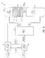
- FIG. 1shows a block diagram of an embodiment for a memory device 100 for implementing a write command sequence, in accordance with the teachings of the present invention.
- the memory device 100is a synchronous flash memory device, in particular, a nonvolatile, electrically sector-erasable (flash), programmable read-only memory.
- flashelectrically sector-erasable
- Other memory devices, including other flash memory devices, having different bit/word densitiescan be used in an embodiment of the teachings of the present invention.
- the memory device 100has been provided in FIG. 1 and simplified in its description to focus on the features of the memory device and its operation, which are helpful in understanding an embodiment of the present invention.
- the memory device 100includes a memory array 102 of non-volatile flash memory cells (not shown), arranged in several addressable banks.
- the memory device 100is arranged containing four memory banks 104 , 106 , 108 and 110 .
- Each memory bankcontains addressable sectors of memory cells, and is organized into four independently erasable blocks (16 total).
- a memory device in an embodiment of the teachings of the present inventionis not limited to a memory device having addressable banks or to memory devices having four memory banks, but may include as many memory banks as necessary for efficient handling of data, dependent on the bit/word densities of the memory device.
- the data stored in the memory device 100can be accessed using externally provided location addresses received by address buffer 112 .
- the addressesare decoded using row address multiplexer circuitry 114 .
- the addressesare also decoded using bank control logic 116 , and row address latch and decode circuitry 118 .
- column address counter and latch circuitry 120couples the received addresses to column decode circuitry 122 .
- Circuit 124provides input/output gating, data mask logic, read data latch circuitry and write driver circuitry. Data is input through data input buffers 126 and output through data output buffers 128 .
- Command and execute logic 130is provided to control the basic operations of the memory device 100 .
- a state machine 132is also provided to control specific operations performed on the memory arrays and cells.
- a status register 134 and an identification register 136can also be provided to output status data.
- the address inputs A 0 –A 11are sampled to select one location in a respective memory bank.
- Other addressingis provided by the bank address inputs, BA 0 and BA 1 , that define a bank to which a command is being applied.
- the BA 01 and BA 02are used as part of the address, increasing the address input.
- the data input and output from memory locations defined by A 0 –A 11 and BA 0 –BA 02move in and out of the memory device 100 through DQ 0 –DQ 15 , which handles bi-directional data.
- nonvolatile memoriesare used to store important information, most non-volatile memory devices do not allow a simple write command to change the data in the memory device. Consequently, as a safety precaution to insure code and data integrity, a specified or predetermined sequence of write operations with specific data and addresses are required to initiate the programming or erasing of data in a location of the memory device. For example, to program or erase a location in memory, a write command sequence directed to the memory device 100 includes a number of cycles, where each cycle has specific or predetermined signal requirements.
- the memory device 100receives a command, an address, data and other control signals.
- the complete addresscan be broken into an address within a bank and a bank identification.
- a commandis defined by a specific status of the control signals or a subset of the control signals externally provided to the memory device.
- additional command and control informationcan be suppled in one cycle by providing a specific code on the data inputs DQ.
- the predetermined information expectedcan be an arbitrary data for that particular cycle.
- the data input buffers 126can be placed in an on state during one of the cycles of a command sequence containing a write command that is received by the memory device 100 .
- various command sequencescan be implemented to include embodiments of the present invention. The description of the various embodiments that follow are presented in terms of a write command sequence. However, other command sequences that make use of data input buffers and include a write command in one or more of its cycles can be used in the various embodiments, as can be understood by those skilled in the art.
- a software command sequence for operating a memory deviceis shown in Table 1.
- the software command sequencesinclude a read command sequence and a write command sequence.
- both a set of read command sequences and a set of write command sequencesinclude command tasks other than the two read operations and the two write operations shown in Table 1.
- specific command, address, data, and control signal RP#are expected, where the command is defined by a set combination of control signals as previously mentioned.
- the notation X for an input signalmeans that for the given cycle no particular information is expected from this input signal. It is essentially “Don't Care” information, which the memory device does not use or need in the given cycle.
- the memory device 100can use the command and address locations to distinguish between a read command sequence and a write command sequence. For instance, on a first cycle of a read command sequence, the inputs to the memory device are an active command with an address 88h. On the other, if the memory device 100 receives a command that is active with an address other than 88h, the memory device 100 prepares for subsequent cycles of a write command sequence. If in the second cycle, information is received on the control signals, address inputs, data inputs, or RP# that is different than expected for the command sequence identified from the first cycle, the memory device 100 will prohibit, i.e., not perform the operation defined in the command sequence, as the memory device has determined the command sequence to be invalid.
- Embodimentsare directed to the generation of a write command sequence to facilitate the command and control of an on state and an off state of data input buffers in a memory device.
- Other embodimentsare directed to the memory devices, memory modules, information handling systems, and other devices that manage the on and off states of data input buffers using an externally generated write command sequence.
- FIG. 2shows a block diagram of an embodiment of functional aspects of a memory device 200 including control circuitry 202 , and data input buffers 204 for using a write command sequence, in accordance with the teachings of the present invention.
- the data input buffers 204are configured in an off state, and are switchable to an on state in response to the control circuitry 202 detecting an externally generated write command sequence having n cycles. The number of cycles used is dependent upon a particular memory device.
- the memory device 200can include a second plurality of data input buffers configured in an off state that are placed in an on state on a k th cycle, k ⁇ n, of the write command sequence in response to the control circuitry 202 detecting a first cycle of the externally generated write command sequence.
- the second plurality of data inputcan be placed in an on state on a k th cycle of the write command sequence in response to the control circuitry 202 detecting a first cycle containing a write command.
- FIG. 2 and the description aboveprovides a functional overview and that actual circuitry may comprise several varied circuits expressed as one functional unit, and that several functional units may be combined into one circuit.
- the control circuitry 202is realized using the command and execute logic 130 , state machine 132 , bank control logic 116 , row address latch and decode circuitry 118 , and latch circuitry 120 of memory device 100 in FIG. 1 .
- the control signals to control circuitry 202include the input signals RP#, CKE, CLK, CS#, WE#, CAS#, and RAS# of FIG. 1 .
- the address provided to memory deviceincludes A 0 –A 11 and BA 0 –BA 1 of memory device 100 .
- Other embodimentscan be realized implementing the functional relations of memory device 200 .
- a processorprovides a write command sequence to the memory device 200 .
- a memory moduleprovides a write command sequence to the memory device 200 based on a write request received by the memory module from a processor or other memory controller.
- the load command unit 302is configured to generate a write command sequence of n cycles, where a write command with associated valid data is generated during a m th cycle, m ⁇ n. For each cycle containing a write command from the m th cycle through the n th cycle, the load command unit 302 generates valid data and address information.
- the last cyclecontains the data or code provided in the write request to the memory module 300 received on the input ports 304 . This last cycle also contains the memory address to which the data or code is to be applied in the memory device for which the write request is intended.
- the load command unit 302is further configured to generate arbitrary data in each cycle containing a write command that is generated before generating the m th cycle.
- the load command unit 302is configured to generate a write command with valid data beginning with a particular cycle depending on the memory device to which the write command sequence is directed. In some embodiments, valid data is provided after the first cycle of the write command sequence. Alternately, valid data is generated by the load command unit 302 on the first cycle containing a write command and in subsequent cycles having a write command. In another embodiment, the valid data is generated by the load command unit 302 on the second cycle containing a write command.
- the memory modulecan be implemented as an integrated circuit in the form of a single integrated circuit or as a chip-set. Further, the memory module is formed using standard integrated circuit processing techniques as is known by those skilled in the art.
- FIG. 4Bshows a block diagram of another embodiment of an information handling system 420 including a processor 422 and a memory device 424 utilizing a write command sequence without a separate load command unit, in accordance with the teachings of the present invention.
- the processor 422is coupled to the memory device 424 and generates control and command signals to the memory device 424 for reading and writing operations on data locations within the memory device 424 in support of the applications for which the processor is directed.
- the memory device 424comprises an embodiment of memory device 200 of FIG. 2 .
- the memory device 424includes a control circuitry 202 for receiving control signals from the processor 422 and data input buffers 204 , which are normally configured in an off state but are switchable to an on state.
- the data input buffers 204are switched to the on state in response to the control circuitry 202 detecting an externally generated write command sequence of n cycles. Further, the control circuitry 202 is also configured to place the data input buffers 204 into an off state upon completing an execution of an operation defined by a write command sequence received from the processor 422 .
- the processor 422generates a n cycle sequence with valid data provided on the second cycle containing a write command, where the processor generated arbitrary data or “Don't Care” data on the cycle with the first write command in the n cycle sequence. It can be appreciated by those skilled in the art that the information handling system 422 can be constructed using any embodiment discussed in connection with the memory device 200 of FIG. 2 as the memory device 424 .
- Table 1provides an embodiment of software command sequences that can be used to optimize the power consumption of memory devices such as non-volatile memories, in particular, Flash memories.
- Embodimentsare directed to the generation of a write command sequence to facilitate the command and control of an on state and an off state of data input buffers in such memory devices.
- a data requirementis not needed for the first cycle, so that valid data is provided for each cycle after the first cycle.
- a particular form of valid datais not required until the second or three cycle.
- valid datais needed during some of the cycles of the write command sequence. During the cycles in which valid data is not required, arbitrary data or “Don't Care” data is provided.
- a method for writing to a memory device 200 of FIG. 2 using a software command sequenceincludes generating a write command sequence of n cycles, and providing valid data directed to a first plurality of data input buffers of the memory device 200 for each cycle after the m th cycle, m ⁇ n.
- the write command sequenceis further generated such that for a second plurality of data input buffers of the memory device 200 , valid is provided on the first cycle of the write command sequence.
- the write command sequenceis generated by a processor or memory controller that is programmed with respect to the requirement for the data input buffers of the memory device for which the write command sequence is being generated, as can be appreciated by those skilled in the art.
- a method for writing to a memory device 200 of FIG. 2 using a software command sequenceincludes generating a write command sequence of n cycles that is directed to providing valid data associated with a write command to each of the data input buffers of the memory device during different cycles.
- This write command sequenceis directed to a memory device whose data input buffers are grouped into R sets, where each set is to be activated to receive valid data in a specified cycle.
- valid datais directed to a j th set of the R sets of data input buffers on a m j th cycle of the write command sequence, 1 ⁇ j ⁇ R and 1 ⁇ m j ⁇ n.
- a memory devicecan have 32 data input buffers, organized as 4 sets of data input buffers, d 1 , d 2 , d 3 , and d 4 , and use an 8 cycle write command sequence.
- the write command sequencecan be generated with valid data directed to d 1 on the third cycle, directed to set d 2 on the fourth cycle, directed to set d 3 on the fifth cycle, and directed to set d 4 on the sixth cycle. Consequently, though the data input buffers in set d 1 must be placed in the on state by the third cycle, the 32 total data input buffers do not need to be placed in the on state until the just prior to the sixth cycle.
- valid datais provided for a second plurality of data input buffers on a k th cycle of the write command sequence, k ⁇ m, where the k th cycle contains a write command. Further, valid data is generated for a third plurality of data input buffers on the j th cycle of the write command sequence, m ⁇ j ⁇ n, the j th cycle containing a write command.
- the software command sequenceis realized as a data signal for a memory device embodied in a set of electrical signals.
- the data signalincludes a sequence of n cycles. Each cycle contains a plurality of data portions.
- a first data portioncontains data representing a command.
- a second data portioncontains data representing a memory address.
- a third data portioncontains data representing data to be stored in the memory, or a code for a memory to perform an operation.
- the code for a memory to perform an operationalso includes codes for subsequent processing of the software command sequence.
- a software command sequenceformatted as a write command sequence, generates arbitrary data for the third data portion in a cycle containing a write command in the first data portion, for the first occurrence of the write command in the n cycle sequence. Subsequently, valid data is provided in the third data portion for cycles containing a write command in the first data portion.
- a write command sequencegenerates arbitrary data for the third data portion in the first one or two cycles that contain a write command in the first data portion. Subsequently, valid data is provided in the third data portion for cycles containing a write command in the first data portion.
- the write command sequencecan be generated with valid data in the third data portion beginning on any cycle of the n cycle sequence.
- each cycle of the 8 cycle software command sequence of Table 1includes a fifth data portion containing data representing a control signal, RP#, having a high (H), a low (L), or a high value set at a particular level (VHH).
- FIG. 6Ashows a method of operating a memory device 200 of FIG. 2 in conjunction with a software command sequence for optimizing power consumption by the memory device 200 in an embodiment according to the teachings of the present invention.
- Operating the memory device 200 in conjunction with such a software command sequenceincludes receiving a write command sequence of n cycles in block 602 , detecting a write command and a valid address in the m th cycle of the write command sequence, m ⁇ n, in block 604 , and placing data input buffers 204 into an on state in response to detecting the write command and the valid address in the m th cycle in block 606 .
- operating the memory device 200includes detecting a write command in the second cycle of a write command sequence.
- operating the memory device 200includes detecting the write command with a valid address on the first cycle of the write command sequence.
- a valid addressis any address other than a predetermined set of addresses that correspond to a read command sequence.
- operating the memory deviceincludes detecting the first cycle containing a write command with a valid address.
- FIG. 6Bshows a method for further operating the memory device 200 of FIG. 2 based on the information contained in the received write command sequence of FIG. 6A in an embodiment according to the teachings of the present invention.
- the methodfurther includes monitoring the n cycles of the received write command sequence in block 612 , determining if information provided in each cycle matches a predetermined criteria in block 614 , performing a program operation or an erase operation as determined from the information provided in the n cycles in block 616 , and placing the data input buffers into an off state upon completing the program operation or the erase operation in block 618 .
- Operating the memory device 200includes taking safety precautions such as prohibiting a write or erase operation if an address monitored while receiving the write command sequence differs from a predetermined address for each cycle.
- the memory device 200monitors each cycle for a predetermined address that is associated with a code indicating a particular type of program or erase operation. For instance, in Table 1, the memory device 200 monitoring the address in the third, fourth and fifth cycles detects addresses that are the same for both a erase setup/confirm operation and a program setup/confirm operation. The addresses for these two operations differ in the sixth cycle. Further in the seventh and eighth cycles, the memory device 200 uses the detected addresses as the row and column (along with a bank address) to identify the memory located to which the determined operation is to be performed. Having monitored the first sixth cycles and detected proper codes and addresses, the memory device 200 takes the addresses of the seventh and eighth cycles as valid or predetermined addresses of memory locations to which a decoded operation will be applied.
- operating memory device 200includes performing other standard operations for a memory device and includes operating the memory device 200 in the various embodiments of memory device 200 as discussed herein.
- a software command sequenceis provided to a memory device, where the software command sequence is constructed by generating a write command sequence of n cycles and providing valid data in each cycle in which a write command is generated after a m th cycle of the write command sequence, where m is less than n.
- the memory devicemaintains its data input buffers in an off state until it receives a write command sequence, at which time, the memory device turns on its data input buffers.
- the memory deviceUpon completion of a program or erase operation defined in the received write command sequence, the memory device then returns its data input buffers to an off state.
- programming and erasing activitiescomprise a relatively small amount of the activity of these memories. Consequently, current usage is significantly reduced having data input buffers normally configured in an off state.
- the structure of the write command sequencealso allows a subset of the data input buffers to be continually in an on state. With a subset of data input buffers continually on, the memory device, if needed, can employ precautionary procedures using these continually on data input buffers to insure that a valid write command sequence is actually being received. At the same time, with the remaining data input buffers normally in an off state, power consumption can still be reduced.
Landscapes
- Read Only Memory (AREA)
Abstract
Description
| TABLE 1 | ||||||||
| FIRST | SECOND | THIRD | FOURTH | FIFTH | SIXTH | SEVENTH | EIGHTH | |
| OPERATION | CYCLE | CYCLE | CYCLE | CYCLE | CYCLE | CYCLE | CYCLE | CYCLE |
| READ DEVICE CONFIGURATION |
| Command | Active | Write | Active | Read | |
| Addr = | 88 h | 90 h | CA (row) | CA (col) | |
| Bank Addr = | X | X | Bank | Bank | |
| DQ = | X | X | X | X | |
| RP# = | H | H | H | H |
| READ STATUS REGISTER |
| Command | Active | Write | Active | Read | |
| Addr = | 88 h | 70 h | X | X | |
| Bank Addr = | X | X | X | X | |
| DQ = | X | X | X | X | |
| RP# = | H | H | H | H |
| ERASE SETUP/CONFIRM |
| Command | Active | Write | Active | Write | Active | Write | Active | Write |
| Addr = | X | 55 h | 55 | 2 Ah | 80 h | 40 h | Row | X |
| Bank Addr = | X | Bank | Bank | Bank | Bank | Bank | Bank | Bank |
| DQ = | X | X | X | 55 h | X | A0 h | X | D0 h |
| RP# = | H | H | H | H | H | H | H | H/VHH |
| PROGRAM SETUP/CONFIRM |
| Command | Active | Write | Active | Write | Active | Write | Active | Write |
| Addr = | X | 55 h | 55 | 2 Ah | 80 h | 40 h | Row | Col |
| Bank Addr = | X | Bank | Bank | Bank | Bank | Bank | Bank | Bank |
| DQ = | X | X | X | 55 h | X | A0 h | X | DIN |
| RP# = | H | H | H | H | H | H | H | H/VHH |
Claims (80)
Priority Applications (2)
| Application Number | Priority Date | Filing Date | Title |
|---|---|---|---|
| US10/156,420US7251711B2 (en) | 2002-05-28 | 2002-05-28 | Apparatus and methods having a command sequence |
| US11/493,127US7305514B2 (en) | 2002-05-28 | 2006-07-26 | Command sequence for optimized power consumption |
Applications Claiming Priority (1)
| Application Number | Priority Date | Filing Date | Title |
|---|---|---|---|
| US10/156,420US7251711B2 (en) | 2002-05-28 | 2002-05-28 | Apparatus and methods having a command sequence |
Related Child Applications (1)
| Application Number | Title | Priority Date | Filing Date |
|---|---|---|---|
| US11/493,127ContinuationUS7305514B2 (en) | 2002-05-28 | 2006-07-26 | Command sequence for optimized power consumption |
Publications (2)
| Publication Number | Publication Date |
|---|---|
| US20030225987A1 US20030225987A1 (en) | 2003-12-04 |
| US7251711B2true US7251711B2 (en) | 2007-07-31 |
Family
ID=29582257
Family Applications (2)
| Application Number | Title | Priority Date | Filing Date |
|---|---|---|---|
| US10/156,420Expired - LifetimeUS7251711B2 (en) | 2002-05-28 | 2002-05-28 | Apparatus and methods having a command sequence |
| US11/493,127Expired - LifetimeUS7305514B2 (en) | 2002-05-28 | 2006-07-26 | Command sequence for optimized power consumption |
Family Applications After (1)
| Application Number | Title | Priority Date | Filing Date |
|---|---|---|---|
| US11/493,127Expired - LifetimeUS7305514B2 (en) | 2002-05-28 | 2006-07-26 | Command sequence for optimized power consumption |
Country Status (1)
| Country | Link |
|---|---|
| US (2) | US7251711B2 (en) |
Cited By (4)
| Publication number | Priority date | Publication date | Assignee | Title |
|---|---|---|---|---|
| US20080184002A1 (en)* | 2007-01-31 | 2008-07-31 | Samsung Electronics Co., Ltd. | Memory system, memory device and command protocol |
| US7644226B1 (en)* | 2006-12-19 | 2010-01-05 | Spansion Llc | System and method for maintaining RAM command timing across phase-shifted time domains |
| US8327044B2 (en)* | 2009-12-14 | 2012-12-04 | Apple Inc. | Transaction ID filtering for buffered programmed input/output (PIO) write acknowledgements |
| US11042492B2 (en) | 2017-10-24 | 2021-06-22 | Rambus Inc. | Memory module with programmable command buffer |
Families Citing this family (7)
| Publication number | Priority date | Publication date | Assignee | Title |
|---|---|---|---|---|
| US4945346A (en) | 1989-08-07 | 1990-07-31 | Schmiemann John P | Audible circuit tracer |
| US7251711B2 (en)* | 2002-05-28 | 2007-07-31 | Micron Technology, Inc. | Apparatus and methods having a command sequence |
| EP1548601A1 (en)* | 2003-12-23 | 2005-06-29 | Stmicroelectronics SA | Memory access control in an electronic apparatus |
| US7460545B1 (en)* | 2004-06-14 | 2008-12-02 | Intel Corporation | Enhanced SDRAM bandwidth usage and memory management for TDM traffic |
| US8028198B2 (en) | 2007-07-30 | 2011-09-27 | Micron Technology, Inc. | Devices, methods, and apparatuses for detection, sensing, and reporting functionality for semiconductor memory |
| TW200923944A (en)* | 2007-11-23 | 2009-06-01 | Skymedi Corp | Non-volatile memory system and its control method |
| TW201132104A (en)* | 2010-03-02 | 2011-09-16 | Wistron Corp | Method for protecting data privacy and wireless communication system |
Citations (46)
| Publication number | Priority date | Publication date | Assignee | Title |
|---|---|---|---|---|
| US4443864A (en) | 1979-10-09 | 1984-04-17 | Texas Instruments Incorporated | Memory system for microprocessor with multiplexed address/data bus |
| US5388248A (en)* | 1992-03-31 | 1995-02-07 | Intel Corporation | Flash memory card including plural flash memories and circuitry for selectively outputting ready/busy signals in different operating modes |
| US5422855A (en)* | 1992-03-31 | 1995-06-06 | Intel Corporation | Flash memory card with all zones chip enable circuitry |
| US5450354A (en)* | 1992-08-31 | 1995-09-12 | Nippon Steel Corporation | Non-volatile semiconductor memory device detachable deterioration of memory cells |
| US5457694A (en)* | 1993-06-25 | 1995-10-10 | Smith; Dale J. | Method and apparatus for analyzing the ATA (IDE) interface |
| US5519847A (en)* | 1993-06-30 | 1996-05-21 | Intel Corporation | Method of pipelining sequential writes in a flash memory |
| US5568426A (en) | 1995-07-26 | 1996-10-22 | Micron Quantum Devices, Inc. | Method and apparatus for performing memory cell verification on a nonvolatile memory circuit |
| US5587961A (en) | 1996-02-16 | 1996-12-24 | Micron Technology, Inc. | Synchronous memory allowing early read command in write to read transitions |
| US5598376A (en) | 1994-12-23 | 1997-01-28 | Micron Technology, Inc. | Distributed write data drivers for burst access memories |
| US5600605A (en) | 1995-06-07 | 1997-02-04 | Micron Technology, Inc. | Auto-activate on synchronous dynamic random access memory |
| US5636173A (en) | 1995-06-07 | 1997-06-03 | Micron Technology, Inc. | Auto-precharge during bank selection |
| US5655105A (en)* | 1995-06-30 | 1997-08-05 | Micron Technology, Inc. | Method and apparatus for multiple latency synchronous pipelined dynamic random access memory |
| US5737258A (en)* | 1995-04-26 | 1998-04-07 | Samsung Electronics Co., Ltd. | Nonvolatile semiconductor memory which is connectable to a DRAM bus |
| US5768287A (en) | 1996-10-24 | 1998-06-16 | Micron Quantum Devices, Inc. | Apparatus and method for programming multistate memory device |
| US5877987A (en) | 1997-02-14 | 1999-03-02 | Micron Technology, Inc. | Method and circuit for self-latching data read lines in the data output path of a semiconductor memory device |
| US5880987A (en) | 1997-07-14 | 1999-03-09 | Micron Technology, Inc. | Architecture and package orientation for high speed memory devices |
| US5890193A (en) | 1995-07-28 | 1999-03-30 | Micron Technology, Inc. | Architecture for state machine for controlling internal operations of flash memory |
| US5974499A (en) | 1997-04-23 | 1999-10-26 | Micron Technology, Inc. | Memory system having read modify write function and method |
| US5986570A (en) | 1997-09-03 | 1999-11-16 | Micron Communications, Inc. | Method for resolving signal collisions between multiple RFID transponders in a field |
| US6044429A (en) | 1997-07-10 | 2000-03-28 | Micron Technology, Inc. | Method and apparatus for collision-free data transfers in a memory device with selectable data or address paths |
| US6075973A (en) | 1998-05-18 | 2000-06-13 | Micron Technology, Inc. | Method of communications in a backscatter system, interrogator, and backscatter communications system |
| US6169474B1 (en) | 1998-04-23 | 2001-01-02 | Micron Technology, Inc. | Method of communications in a backscatter system, interrogator, and backscatter communications system |
| US6253340B1 (en) | 1998-06-08 | 2001-06-26 | Micron Technology, Inc. | Integrated circuit implementing internally generated commands |
| US20010008495A1 (en) | 1998-08-25 | 2001-07-19 | Mitsubishi Denki Kabushiki Kaisha | Synchronous Semiconductor memory device |
| US6278654B1 (en) | 2000-06-30 | 2001-08-21 | Micron Technology, Inc. | Active terminate command in synchronous flash memory |
| US6307772B1 (en) | 1999-09-29 | 2001-10-23 | Mitsubishi Denki Kabushiki Kaisha | Static type semiconductor memory device for lower current consumption |
| US6307779B1 (en) | 2000-07-28 | 2001-10-23 | Micron Technology, Inc. | Method and circuitry for bank tracking in write command sequence |
| US6314049B1 (en) | 2000-03-30 | 2001-11-06 | Micron Technology, Inc. | Elimination of precharge operation in synchronous flash memory |
| US6324211B1 (en) | 1998-04-24 | 2001-11-27 | Micron Technology, Inc. | Interrogators communication systems communication methods and methods of processing a communication signal |
| US6381180B1 (en) | 1994-12-23 | 2002-04-30 | Micron Technology, Inc. | Distributed write data drivers for burst access memories |
| US6442076B1 (en) | 2000-06-30 | 2002-08-27 | Micron Technology, Inc. | Flash memory with multiple status reading capability |
| US20020131085A1 (en)* | 2001-03-15 | 2002-09-19 | Kazunori Kobayashi | Nonvolatile memory life prolonging circuit and image forming apparatus |
| US6459726B1 (en) | 1998-04-24 | 2002-10-01 | Micron Technology, Inc. | Backscatter interrogators, communication systems and backscatter communication methods |
| US6466507B2 (en) | 1999-01-05 | 2002-10-15 | Micron Technology, Inc. | DRAM with intermediate storage cache and separate read and write I/O |
| US20020184579A1 (en)* | 2001-04-23 | 2002-12-05 | Alvarez Manuel J. | System and method for recognizing and configuring devices embedded on memory modules |
| US20030023840A1 (en) | 2001-07-25 | 2003-01-30 | Micron Technology, Inc. | Power up initialization for memory |
| US6525971B2 (en) | 1995-06-30 | 2003-02-25 | Micron Technology, Inc. | Distributed write data drivers for burst access memories |
| US6535422B2 (en)* | 2000-12-28 | 2003-03-18 | Hitachi, Ltd. | Nonvolatile memory system |
| US6549994B1 (en) | 1998-07-07 | 2003-04-15 | Samsung Electronics Co., Ltd. | Semiconductor memory device capable of performing a write operation 1 or 2 cycles after receiving a write command without a dead cycle |
| US6580659B1 (en) | 2000-08-25 | 2003-06-17 | Micron Technology, Inc. | Burst read addressing in a non-volatile memory device |
| US6615307B1 (en) | 2000-05-10 | 2003-09-02 | Micron Technology, Inc. | Flash with consistent latency for read operations |
| US6625081B2 (en) | 2001-08-13 | 2003-09-23 | Micron Technology, Inc. | Synchronous flash memory with virtual segment architecture |
| US6658552B1 (en) | 1998-10-23 | 2003-12-02 | Micron Technology, Inc. | Processing system with separate general purpose execution unit and data string manipulation unit |
| US6691204B1 (en) | 2000-08-25 | 2004-02-10 | Micron Technology, Inc. | Burst write in a non-volatile memory device |
| US6748482B1 (en) | 2000-09-27 | 2004-06-08 | Intel Corporation | Multiple non-contiguous block erase in flash memory |
| US20060265564A1 (en) | 2002-05-28 | 2006-11-23 | Micron Technology, Inc. | Software command sequence for optimized power consumption |
Family Cites Families (2)
| Publication number | Priority date | Publication date | Assignee | Title |
|---|---|---|---|---|
| US6307049B1 (en)* | 1998-09-30 | 2001-10-23 | The Procter & Gamble Co. | Heterocyclic 2-substituted ketoamides |
| JP4055266B2 (en)* | 1998-10-13 | 2008-03-05 | 株式会社日立製作所 | Optical measuring device |
- 2002
- 2002-05-28USUS10/156,420patent/US7251711B2/ennot_activeExpired - Lifetime
- 2006
- 2006-07-26USUS11/493,127patent/US7305514B2/ennot_activeExpired - Lifetime
Patent Citations (72)
| Publication number | Priority date | Publication date | Assignee | Title |
|---|---|---|---|---|
| US4443864A (en) | 1979-10-09 | 1984-04-17 | Texas Instruments Incorporated | Memory system for microprocessor with multiplexed address/data bus |
| US5388248A (en)* | 1992-03-31 | 1995-02-07 | Intel Corporation | Flash memory card including plural flash memories and circuitry for selectively outputting ready/busy signals in different operating modes |
| US5422855A (en)* | 1992-03-31 | 1995-06-06 | Intel Corporation | Flash memory card with all zones chip enable circuitry |
| US5450354A (en)* | 1992-08-31 | 1995-09-12 | Nippon Steel Corporation | Non-volatile semiconductor memory device detachable deterioration of memory cells |
| US5457694A (en)* | 1993-06-25 | 1995-10-10 | Smith; Dale J. | Method and apparatus for analyzing the ATA (IDE) interface |
| US5519847A (en)* | 1993-06-30 | 1996-05-21 | Intel Corporation | Method of pipelining sequential writes in a flash memory |
| US5757703A (en) | 1994-12-23 | 1998-05-26 | Micron Technology, Inc. | Distributed write data drivers for burst access memories |
| US5598376A (en) | 1994-12-23 | 1997-01-28 | Micron Technology, Inc. | Distributed write data drivers for burst access memories |
| US6381180B1 (en) | 1994-12-23 | 2002-04-30 | Micron Technology, Inc. | Distributed write data drivers for burst access memories |
| US5737258A (en)* | 1995-04-26 | 1998-04-07 | Samsung Electronics Co., Ltd. | Nonvolatile semiconductor memory which is connectable to a DRAM bus |
| US5600605A (en) | 1995-06-07 | 1997-02-04 | Micron Technology, Inc. | Auto-activate on synchronous dynamic random access memory |
| US5636173A (en) | 1995-06-07 | 1997-06-03 | Micron Technology, Inc. | Auto-precharge during bank selection |
| US5655105A (en)* | 1995-06-30 | 1997-08-05 | Micron Technology, Inc. | Method and apparatus for multiple latency synchronous pipelined dynamic random access memory |
| US6525971B2 (en) | 1995-06-30 | 2003-02-25 | Micron Technology, Inc. | Distributed write data drivers for burst access memories |
| US5677879A (en) | 1995-07-26 | 1997-10-14 | Micron Quantum Devices, Inc. | Method and apparatus for performing memory cell verification on a nonvolatile memory circuit |
| US5568426A (en) | 1995-07-26 | 1996-10-22 | Micron Quantum Devices, Inc. | Method and apparatus for performing memory cell verification on a nonvolatile memory circuit |
| US6356974B2 (en) | 1995-07-28 | 2002-03-12 | Micron Technology, Inc. | Architecture for state machine for controlling internal operations of flash memory |
| US5890193A (en) | 1995-07-28 | 1999-03-30 | Micron Technology, Inc. | Architecture for state machine for controlling internal operations of flash memory |
| US5587961A (en) | 1996-02-16 | 1996-12-24 | Micron Technology, Inc. | Synchronous memory allowing early read command in write to read transitions |
| US5673233A (en) | 1996-02-16 | 1997-09-30 | Micron Technology, Inc. | Synchronous memory allowing early read command in write to read transitions |
| US5768287A (en) | 1996-10-24 | 1998-06-16 | Micron Quantum Devices, Inc. | Apparatus and method for programming multistate memory device |
| US6175937B1 (en) | 1996-10-24 | 2001-01-16 | Micron Technology, Inc. | Apparatus and method for programming multistate memory device |
| US5877987A (en) | 1997-02-14 | 1999-03-02 | Micron Technology, Inc. | Method and circuit for self-latching data read lines in the data output path of a semiconductor memory device |
| US5986944A (en) | 1997-02-14 | 1999-11-16 | Micron Technology, Inc. | Method and apparatus using a data read latch circuit in a semiconductor device |
| US6049489A (en) | 1997-02-14 | 2000-04-11 | Micron Technology, Inc. | Methods using a data read latch circuit in a semiconductor device |
| US5974499A (en) | 1997-04-23 | 1999-10-26 | Micron Technology, Inc. | Memory system having read modify write function and method |
| US6611885B2 (en) | 1997-07-10 | 2003-08-26 | Micron Technology, Inc. | Method and apparatus for synchronous data transfers in a memory device with selectable data or address paths |
| US6415340B1 (en) | 1997-07-10 | 2002-07-02 | Micron Technology, Inc. | Method and apparatus for synchronous data transfers in a memory device with selectable data or address paths |
| US6044429A (en) | 1997-07-10 | 2000-03-28 | Micron Technology, Inc. | Method and apparatus for collision-free data transfers in a memory device with selectable data or address paths |
| US6556483B2 (en) | 1997-07-10 | 2003-04-29 | Micron Technology, Inc. | Method and apparatus for synchronous data transfers in a memory device with selectable data or address paths |
| US6614698B2 (en) | 1997-07-10 | 2003-09-02 | Micron Technology, Inc. | Method and apparatus for synchronous data transfers in a memory device with selectable data or address paths |
| US6560668B2 (en) | 1997-07-10 | 2003-05-06 | Micron Technology, Inc. | Method and apparatus for reading write-modified read data in memory device providing synchronous data transfers |
| US6272608B1 (en) | 1997-07-10 | 2001-08-07 | Micron Technology, Inc. | Method and apparatus for synchronous data transfers in a memory device with lookahead logic for detecting latency intervals |
| US5880987A (en) | 1997-07-14 | 1999-03-09 | Micron Technology, Inc. | Architecture and package orientation for high speed memory devices |
| US6043107A (en) | 1997-07-14 | 2000-03-28 | Micron Technology, Inc. | Method for producing an integrated circuit assembly |
| US5986570A (en) | 1997-09-03 | 1999-11-16 | Micron Communications, Inc. | Method for resolving signal collisions between multiple RFID transponders in a field |
| US6265962B1 (en) | 1997-09-03 | 2001-07-24 | Micron Technology, Inc. | Method for resolving signal collisions between multiple RFID transponders in a field |
| US6091319A (en) | 1997-09-03 | 2000-07-18 | Micron Technology, Inc. | Method for resolving signals collisions between multiple RFID transponders in a field |
| US6169474B1 (en) | 1998-04-23 | 2001-01-02 | Micron Technology, Inc. | Method of communications in a backscatter system, interrogator, and backscatter communications system |
| US6324211B1 (en) | 1998-04-24 | 2001-11-27 | Micron Technology, Inc. | Interrogators communication systems communication methods and methods of processing a communication signal |
| US6459726B1 (en) | 1998-04-24 | 2002-10-01 | Micron Technology, Inc. | Backscatter interrogators, communication systems and backscatter communication methods |
| US6229987B1 (en) | 1998-05-18 | 2001-05-08 | Micron Technology, Inc. | Method of communications in a backscatter system, interrogator, and backscatter communications system |
| US6075973A (en) | 1998-05-18 | 2000-06-13 | Micron Technology, Inc. | Method of communications in a backscatter system, interrogator, and backscatter communications system |
| US6253340B1 (en) | 1998-06-08 | 2001-06-26 | Micron Technology, Inc. | Integrated circuit implementing internally generated commands |
| US6526533B1 (en) | 1998-06-08 | 2003-02-25 | Micron Technology, Inc. | Semiconductor memory implementing internally generated commands |
| US6549994B1 (en) | 1998-07-07 | 2003-04-15 | Samsung Electronics Co., Ltd. | Semiconductor memory device capable of performing a write operation 1 or 2 cycles after receiving a write command without a dead cycle |
| US20010008495A1 (en) | 1998-08-25 | 2001-07-19 | Mitsubishi Denki Kabushiki Kaisha | Synchronous Semiconductor memory device |
| US6658552B1 (en) | 1998-10-23 | 2003-12-02 | Micron Technology, Inc. | Processing system with separate general purpose execution unit and data string manipulation unit |
| US6466507B2 (en) | 1999-01-05 | 2002-10-15 | Micron Technology, Inc. | DRAM with intermediate storage cache and separate read and write I/O |
| US6307772B1 (en) | 1999-09-29 | 2001-10-23 | Mitsubishi Denki Kabushiki Kaisha | Static type semiconductor memory device for lower current consumption |
| US6314049B1 (en) | 2000-03-30 | 2001-11-06 | Micron Technology, Inc. | Elimination of precharge operation in synchronous flash memory |
| US6496444B2 (en) | 2000-03-30 | 2002-12-17 | Micron Technology, Inc. | Elimination of precharge operation in synchronous flash memory |
| US6615307B1 (en) | 2000-05-10 | 2003-09-02 | Micron Technology, Inc. | Flash with consistent latency for read operations |
| US6657899B2 (en) | 2000-06-30 | 2003-12-02 | Micron Technology, Inc. | Flash memory with multiple status reading capability |
| US6442076B1 (en) | 2000-06-30 | 2002-08-27 | Micron Technology, Inc. | Flash memory with multiple status reading capability |
| US6438068B1 (en) | 2000-06-30 | 2002-08-20 | Micron Technology, Inc. | Active terminate command in synchronous flash memory |
| US6278654B1 (en) | 2000-06-30 | 2001-08-21 | Micron Technology, Inc. | Active terminate command in synchronous flash memory |
| US6606269B2 (en) | 2000-06-30 | 2003-08-12 | Micron Technology, Inc. | Flash memory with multiple status reading capability |
| US6307779B1 (en) | 2000-07-28 | 2001-10-23 | Micron Technology, Inc. | Method and circuitry for bank tracking in write command sequence |
| US6459617B1 (en) | 2000-07-28 | 2002-10-01 | Micron Technology, Inc. | Method and circuitry for bank tracking in write command sequence |
| US6580659B1 (en) | 2000-08-25 | 2003-06-17 | Micron Technology, Inc. | Burst read addressing in a non-volatile memory device |
| US6654313B2 (en) | 2000-08-25 | 2003-11-25 | Micron Technology, Inc. | Burst read addressing in a non-volatile memory device |
| US6691204B1 (en) | 2000-08-25 | 2004-02-10 | Micron Technology, Inc. | Burst write in a non-volatile memory device |
| US6748482B1 (en) | 2000-09-27 | 2004-06-08 | Intel Corporation | Multiple non-contiguous block erase in flash memory |
| US6535422B2 (en)* | 2000-12-28 | 2003-03-18 | Hitachi, Ltd. | Nonvolatile memory system |
| US20020131085A1 (en)* | 2001-03-15 | 2002-09-19 | Kazunori Kobayashi | Nonvolatile memory life prolonging circuit and image forming apparatus |
| US20020184579A1 (en)* | 2001-04-23 | 2002-12-05 | Alvarez Manuel J. | System and method for recognizing and configuring devices embedded on memory modules |
| US20030023840A1 (en) | 2001-07-25 | 2003-01-30 | Micron Technology, Inc. | Power up initialization for memory |
| US6625081B2 (en) | 2001-08-13 | 2003-09-23 | Micron Technology, Inc. | Synchronous flash memory with virtual segment architecture |
| US6654307B2 (en) | 2001-08-13 | 2003-11-25 | Micron Technology, Inc. | DDR synchronous flash memory with virtual segment architecture |
| US6667932B2 (en) | 2001-08-13 | 2003-12-23 | Micron Technology, Inc. | Synchronous flash memory with virtual segment architecture |
| US20060265564A1 (en) | 2002-05-28 | 2006-11-23 | Micron Technology, Inc. | Software command sequence for optimized power consumption |
Non-Patent Citations (1)
| Title |
|---|
| Mills et al., Feb. 15-17, 1995, IEEE, pp. 120-121.* |
Cited By (7)
| Publication number | Priority date | Publication date | Assignee | Title |
|---|---|---|---|---|
| US7644226B1 (en)* | 2006-12-19 | 2010-01-05 | Spansion Llc | System and method for maintaining RAM command timing across phase-shifted time domains |
| US20080184002A1 (en)* | 2007-01-31 | 2008-07-31 | Samsung Electronics Co., Ltd. | Memory system, memory device and command protocol |
| US8045405B2 (en)* | 2007-01-31 | 2011-10-25 | Samsung Electronics Co., Ltd. | Memory system, memory device and command protocol |
| US8327044B2 (en)* | 2009-12-14 | 2012-12-04 | Apple Inc. | Transaction ID filtering for buffered programmed input/output (PIO) write acknowledgements |
| US11042492B2 (en) | 2017-10-24 | 2021-06-22 | Rambus Inc. | Memory module with programmable command buffer |
| US11615037B2 (en) | 2017-10-24 | 2023-03-28 | Rambus Inc. | Memory module with programmable command buffer |
| US11886360B2 (en) | 2017-10-24 | 2024-01-30 | Rambus Inc. | Memory module with programmable command buffer |
Also Published As
| Publication number | Publication date |
|---|---|
| US20060265564A1 (en) | 2006-11-23 |
| US7305514B2 (en) | 2007-12-04 |
| US20030225987A1 (en) | 2003-12-04 |
Similar Documents
| Publication | Publication Date | Title |
|---|---|---|
| US7305514B2 (en) | Command sequence for optimized power consumption | |
| JP3947781B2 (en) | Program algorithm for low voltage single power flash memory | |
| US7620768B2 (en) | Multiple erase block tagging in a flash memory device | |
| US5802552A (en) | System and method for allocating and sharingpage buffers for a flash memory device | |
| US5761128A (en) | Non-volatile semiconductor memory device | |
| US5414825A (en) | Method of programming a semiconductor memory device within a microcomputer address space | |
| US5623620A (en) | Special test modes for a page buffer shared resource in a memory device | |
| KR100472741B1 (en) | Bank architecture for a non-volatile memory enabling simultaneous reading and writing | |
| US5732017A (en) | Combined program and data nonvolatile memory with concurrent program-read/data write capability | |
| US5808946A (en) | Parallel processing redundancy scheme for faster access times and lower die area | |
| JPH06333391A (en) | Synchronous semiconductor memory | |
| JP2000163988A (en) | Semiconductor storage device | |
| US5893135A (en) | Flash memory array with two interfaces for responding to RAS and CAS signals | |
| US7873753B2 (en) | Memory subsystem capable of accessing a plurality of memory bank identifications and method thereof | |
| JPH06275095A (en) | Semiconductor memory and writing method for redundant address | |
| US20050013162A1 (en) | Nonvolatile semiconductor memory device and one-time programming control method thereof | |
| US5805510A (en) | Data erase mechanism for nonvolatile memory of boot block type | |
| US6707735B2 (en) | Semiconductor memory device | |
| US8423701B2 (en) | Flash memory device with a low pin count (LPC) communication interface | |
| US7161870B2 (en) | Synchronous flash memory command sequence | |
| KR100444703B1 (en) | Memory device having high bus efficiency of network and the operation method thereof and memory system including the same | |
| US20250245174A1 (en) | Signal processing circuit, semiconductor apparatus and data processing system including the signal processing circuit | |
| US6807084B1 (en) | FeRAM memory device | |
| US20240347112A1 (en) | Memory performing reset operation and operating method thereof | |
| JP4209708B2 (en) | Semiconductor memory device |
Legal Events
| Date | Code | Title | Description |
|---|---|---|---|
| AS | Assignment | Owner name:MICRON TECHNOLOGY, INC., IDAHO Free format text:ASSIGNMENT OF ASSIGNORS INTEREST;ASSIGNOR:ROOHPARVAR, FRANKIE FARIBORZ;REEL/FRAME:012951/0079 Effective date:20020506 | |
| FEPP | Fee payment procedure | Free format text:PAYOR NUMBER ASSIGNED (ORIGINAL EVENT CODE: ASPN); ENTITY STATUS OF PATENT OWNER: LARGE ENTITY | |
| STCF | Information on status: patent grant | Free format text:PATENTED CASE | |
| CC | Certificate of correction | ||
| FPAY | Fee payment | Year of fee payment:4 | |
| FPAY | Fee payment | Year of fee payment:8 | |
| AS | Assignment | Owner name:U.S. BANK NATIONAL ASSOCIATION, AS COLLATERAL AGENT, CALIFORNIA Free format text:SECURITY INTEREST;ASSIGNOR:MICRON TECHNOLOGY, INC.;REEL/FRAME:038669/0001 Effective date:20160426 Owner name:U.S. BANK NATIONAL ASSOCIATION, AS COLLATERAL AGEN Free format text:SECURITY INTEREST;ASSIGNOR:MICRON TECHNOLOGY, INC.;REEL/FRAME:038669/0001 Effective date:20160426 | |
| AS | Assignment | Owner name:MORGAN STANLEY SENIOR FUNDING, INC., AS COLLATERAL AGENT, MARYLAND Free format text:PATENT SECURITY AGREEMENT;ASSIGNOR:MICRON TECHNOLOGY, INC.;REEL/FRAME:038954/0001 Effective date:20160426 Owner name:MORGAN STANLEY SENIOR FUNDING, INC., AS COLLATERAL Free format text:PATENT SECURITY AGREEMENT;ASSIGNOR:MICRON TECHNOLOGY, INC.;REEL/FRAME:038954/0001 Effective date:20160426 | |
| AS | Assignment | Owner name:U.S. BANK NATIONAL ASSOCIATION, AS COLLATERAL AGENT, CALIFORNIA Free format text:CORRECTIVE ASSIGNMENT TO CORRECT THE REPLACE ERRONEOUSLY FILED PATENT #7358718 WITH THE CORRECT PATENT #7358178 PREVIOUSLY RECORDED ON REEL 038669 FRAME 0001. ASSIGNOR(S) HEREBY CONFIRMS THE SECURITY INTEREST;ASSIGNOR:MICRON TECHNOLOGY, INC.;REEL/FRAME:043079/0001 Effective date:20160426 Owner name:U.S. BANK NATIONAL ASSOCIATION, AS COLLATERAL AGEN Free format text:CORRECTIVE ASSIGNMENT TO CORRECT THE REPLACE ERRONEOUSLY FILED PATENT #7358718 WITH THE CORRECT PATENT #7358178 PREVIOUSLY RECORDED ON REEL 038669 FRAME 0001. ASSIGNOR(S) HEREBY CONFIRMS THE SECURITY INTEREST;ASSIGNOR:MICRON TECHNOLOGY, INC.;REEL/FRAME:043079/0001 Effective date:20160426 | |
| AS | Assignment | Owner name:JPMORGAN CHASE BANK, N.A., AS COLLATERAL AGENT, ILLINOIS Free format text:SECURITY INTEREST;ASSIGNORS:MICRON TECHNOLOGY, INC.;MICRON SEMICONDUCTOR PRODUCTS, INC.;REEL/FRAME:047540/0001 Effective date:20180703 Owner name:JPMORGAN CHASE BANK, N.A., AS COLLATERAL AGENT, IL Free format text:SECURITY INTEREST;ASSIGNORS:MICRON TECHNOLOGY, INC.;MICRON SEMICONDUCTOR PRODUCTS, INC.;REEL/FRAME:047540/0001 Effective date:20180703 | |
| AS | Assignment | Owner name:MICRON TECHNOLOGY, INC., IDAHO Free format text:RELEASE BY SECURED PARTY;ASSIGNOR:U.S. BANK NATIONAL ASSOCIATION, AS COLLATERAL AGENT;REEL/FRAME:047243/0001 Effective date:20180629 | |
| MAFP | Maintenance fee payment | Free format text:PAYMENT OF MAINTENANCE FEE, 12TH YEAR, LARGE ENTITY (ORIGINAL EVENT CODE: M1553); ENTITY STATUS OF PATENT OWNER: LARGE ENTITY Year of fee payment:12 | |
| AS | Assignment | Owner name:MICRON TECHNOLOGY, INC., IDAHO Free format text:RELEASE BY SECURED PARTY;ASSIGNOR:MORGAN STANLEY SENIOR FUNDING, INC., AS COLLATERAL AGENT;REEL/FRAME:050937/0001 Effective date:20190731 | |
| AS | Assignment | Owner name:MICRON TECHNOLOGY, INC., IDAHO Free format text:RELEASE BY SECURED PARTY;ASSIGNOR:JPMORGAN CHASE BANK, N.A., AS COLLATERAL AGENT;REEL/FRAME:051028/0001 Effective date:20190731 Owner name:MICRON SEMICONDUCTOR PRODUCTS, INC., IDAHO Free format text:RELEASE BY SECURED PARTY;ASSIGNOR:JPMORGAN CHASE BANK, N.A., AS COLLATERAL AGENT;REEL/FRAME:051028/0001 Effective date:20190731 |