US7250989B2 - Substrate bonding apparatus having alignment system with one end provided inside vacuum chamber for liquid crystal display device - Google Patents
Substrate bonding apparatus having alignment system with one end provided inside vacuum chamber for liquid crystal display deviceDownload PDFInfo
- Publication number
- US7250989B2 US7250989B2US11/043,042US4304205AUS7250989B2US 7250989 B2US7250989 B2US 7250989B2US 4304205 AUS4304205 AUS 4304205AUS 7250989 B2US7250989 B2US 7250989B2
- Authority
- US
- United States
- Prior art keywords
- alignment
- substrates
- substrate
- alignment system
- stage
- Prior art date
- Legal status (The legal status is an assumption and is not a legal conclusion. Google has not performed a legal analysis and makes no representation as to the accuracy of the status listed.)
- Expired - Lifetime, expires
Links
Images


Classifications
- B—PERFORMING OPERATIONS; TRANSPORTING
- B32—LAYERED PRODUCTS
- B32B—LAYERED PRODUCTS, i.e. PRODUCTS BUILT-UP OF STRATA OF FLAT OR NON-FLAT, e.g. CELLULAR OR HONEYCOMB, FORM
- B32B38/00—Ancillary operations in connection with laminating processes
- B32B38/18—Handling of layers or the laminate
- B32B38/1825—Handling of layers or the laminate characterised by the control or constructional features of devices for tensioning, stretching or registration
- B32B38/1833—Positioning, e.g. registration or centering
- B32B38/1841—Positioning, e.g. registration or centering during laying up
- B—PERFORMING OPERATIONS; TRANSPORTING
- B32—LAYERED PRODUCTS
- B32B—LAYERED PRODUCTS, i.e. PRODUCTS BUILT-UP OF STRATA OF FLAT OR NON-FLAT, e.g. CELLULAR OR HONEYCOMB, FORM
- B32B2309/00—Parameters for the laminating or treatment process; Apparatus details
- B32B2309/60—In a particular environment
- B32B2309/68—Vacuum
- B—PERFORMING OPERATIONS; TRANSPORTING
- B32—LAYERED PRODUCTS
- B32B—LAYERED PRODUCTS, i.e. PRODUCTS BUILT-UP OF STRATA OF FLAT OR NON-FLAT, e.g. CELLULAR OR HONEYCOMB, FORM
- B32B2457/00—Electrical equipment
- B32B2457/20—Displays, e.g. liquid crystal displays, plasma displays
- B—PERFORMING OPERATIONS; TRANSPORTING
- B32—LAYERED PRODUCTS
- B32B—LAYERED PRODUCTS, i.e. PRODUCTS BUILT-UP OF STRATA OF FLAT OR NON-FLAT, e.g. CELLULAR OR HONEYCOMB, FORM
- B32B2457/00—Electrical equipment
- B32B2457/20—Displays, e.g. liquid crystal displays, plasma displays
- B32B2457/202—LCD, i.e. liquid crystal displays
- B—PERFORMING OPERATIONS; TRANSPORTING
- B32—LAYERED PRODUCTS
- B32B—LAYERED PRODUCTS, i.e. PRODUCTS BUILT-UP OF STRATA OF FLAT OR NON-FLAT, e.g. CELLULAR OR HONEYCOMB, FORM
- B32B37/00—Methods or apparatus for laminating, e.g. by curing or by ultrasonic bonding
- B32B37/0046—Methods or apparatus for laminating, e.g. by curing or by ultrasonic bonding characterised by constructional aspects of the apparatus
- G—PHYSICS
- G02—OPTICS
- G02F—OPTICAL DEVICES OR ARRANGEMENTS FOR THE CONTROL OF LIGHT BY MODIFICATION OF THE OPTICAL PROPERTIES OF THE MEDIA OF THE ELEMENTS INVOLVED THEREIN; NON-LINEAR OPTICS; FREQUENCY-CHANGING OF LIGHT; OPTICAL LOGIC ELEMENTS; OPTICAL ANALOGUE/DIGITAL CONVERTERS
- G02F1/00—Devices or arrangements for the control of the intensity, colour, phase, polarisation or direction of light arriving from an independent light source, e.g. switching, gating or modulating; Non-linear optics
- G02F1/01—Devices or arrangements for the control of the intensity, colour, phase, polarisation or direction of light arriving from an independent light source, e.g. switching, gating or modulating; Non-linear optics for the control of the intensity, phase, polarisation or colour
- G02F1/13—Devices or arrangements for the control of the intensity, colour, phase, polarisation or direction of light arriving from an independent light source, e.g. switching, gating or modulating; Non-linear optics for the control of the intensity, phase, polarisation or colour based on liquid crystals, e.g. single liquid crystal display cells
- G02F1/133—Constructional arrangements; Operation of liquid crystal cells; Circuit arrangements
- G02F1/1333—Constructional arrangements; Manufacturing methods
- G02F1/133354—Arrangements for aligning or assembling substrates
- Y—GENERAL TAGGING OF NEW TECHNOLOGICAL DEVELOPMENTS; GENERAL TAGGING OF CROSS-SECTIONAL TECHNOLOGIES SPANNING OVER SEVERAL SECTIONS OF THE IPC; TECHNICAL SUBJECTS COVERED BY FORMER USPC CROSS-REFERENCE ART COLLECTIONS [XRACs] AND DIGESTS
- Y10—TECHNICAL SUBJECTS COVERED BY FORMER USPC
- Y10T—TECHNICAL SUBJECTS COVERED BY FORMER US CLASSIFICATION
- Y10T156/00—Adhesive bonding and miscellaneous chemical manufacture
- Y10T156/17—Surface bonding means and/or assemblymeans with work feeding or handling means
- Y10T156/1702—For plural parts or plural areas of single part
- Y10T156/1744—Means bringing discrete articles into assembled relationship
Definitions
- the present inventionrelates to a bonding apparatus, and more particularly, to a substrate bonding apparatus for bonding substrates to each other during the manufacturing of a liquid crystal display (LCD) device.
- LCDliquid crystal display
- LCDliquid crystal display
- PDPplasma display panel
- ELDelectro luminescent display
- VFDvacuum fluorescent display
- LCD deviceshas been commonly used as a mobile image display device to replace cathode ray tube (CRT) devices.
- LCD devicesare commonly used for monitors of notebook computers, and as monitors of computers and televisions. In order to use LCD devices as general image displays, operational characteristics of low weight, thin profile, and low power consumption must be maintained.
- a method for manufacturing an LCD devicemay be divided into two catagories: liquid crystal injecting and liquid crystal dispensing.
- the liquid crystal injecting typeincludes steps of forming a sealant pattern on a first substrate to form an injection inlet, bonding the first substrate to a second substrate in a vacuum state, and injecting liquid crystal material through the injection inlet.
- the liquid crystal dispensing methodwhich is disclosed in Japanese Patent Application Nos. 11-089612 and 11-172903, includes steps of dispensing liquid crystal material on a first substrate, arranging a second substrate over the first substrate, and moving the first and second substrates, thereby bonding the first and second substrates to each other in a vacuum state.
- the liquid crystal dispensing methodis advantageous in that various steps, such as forming a liquid crystal material injection inlet, injecting the liquid crystal material, and sealing the injection inlet can be omitted.
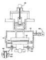
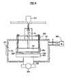
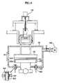
- FIG. 1 and FIG. 2illustrate a related art vacuum bonding device, to which the prior art liquid crystal dispensing method is applied.
- the related art vacuum bonding deviceincludes a frame 10 forming the exterior, a stage part 22 and 21 , a sealant dispenser (not shown), a liquid crystal dispenser 30 , a chamber part 32 and 31 , a chamber moving system, a stage moving system, an alignment system and a vacuum pump 60 .
- the stage partis divided into lower and upper stages 22 and 21 , and the sealant dispenser and the liquid crystal dispenser 30 are provided at a side of location where a bonding process is carried out.
- the chamber partis divided into lower and upper chamber units 32 and 31 that are to be combined.
- the chamber moving systemincludes a driving motor 40 that is driven to selectively move the lower chamber unit 32 to a location at which the bonding process is carried out, or to a location at which the dispensing of the sealant or the liquid crystal occurs.
- the stage moving systemincludes another driving motor 50 that is driven to selectively move the upper stage 21 to the upper or lower part.
- the vacuum pump 60is connected to a tube that is connected to the inside of the upper chamber unit 31 so as to provide an air inhalation to the inside of the upper chamber unit 31 for maintaining the upper chamber unit in the vacuum state.
- the alignment systemincludes an align camera 70 that checks an alignment state between the substrate 52 (hereinafter, referenced as “second substrate”) fixed to the upper stage 21 , and the substrate 51 (hereinafter, referenced as “first substrate”) fixed to the lower stage 22 .
- the upper chamber unitis provided with a through hole 31 a that checks the alignment state between the substrates through the align camera 70 .
- the second substrate 52is loaded to the upper stage 21 , and is fixed thereto.
- the first substrate 51is loaded to the lower stage 22 , and is fixed thereto.
- the lower chamber unit 32having the lower stage 22 , is moved by the chamber moving system 40 to a processing location for depositing the sealant and dispensing the liquid crystal, as shown in FIG. 1 .
- the lower chamber unit 32is moved to a processing location at which the substrates are bonded to each other, as shown in FIG. 2 .
- the lower and upper chamber units 32 and 31are assembled together by the chamber moving system 40 to form a vacuum tight seal, and the vacuum pump 60 is driven so as to make the vacuum state.
- the upper stage 21is moved downwardly, and is positioned at a location for aligning each substrate 51 and 52 .
- the align camera 70checks each align mark of the first and second substrates 51 and 52 , respectively fixed to each stage, through a hole provided in the upper chamber unit 31 and a through hole 21 a provided in the upper stage 21 .
- displacement of each substrateis checked by the align camera 70 , and then is calculated to a numeral value.
- each substrateis aligned in controlling the stage moving system according to the numeral value.
- the upper stage 21is moved further downward by the stage moving system 50 .
- the second substrate 52 fixed to the upper stage 21is contacted to the first substrate 51 fixed to the lower stage 22 , and then a constant pressure is applied to the substrates, thereby bonding the substrates to each other.
- the related art bonding device of the LCD devicehas the following problems.
- the align accuracyis improved in that the align camera can exactly check the align state of the substrates.
- a distance (L 1 )is maintained between the lens of the align camera and an external surface of the upper chamber unit, so that it is hard to exactly check the align state of each substrate.
- the align accuracyis deteriorated in that the distance becomes great between the lens of the align camera and the external surface of the upper chamber unit.
- a distance (L 2 )is generated between an internal surface of the upper chamber unit and the align mark of the substrate, thereby deteriorating the align accuracy.
- only one align camerais used for checking the align marks of each substrate in the related art bonding device, thereby increasing processing time.
- the alignment systemhaving a structure that is suitable for manufacturing the large-sized LCD device has been actively studied and is needed for large-sized LCD devices.
- the present inventionis directed to a substrate bonding apparatus that substantially obviates one or more problems due to limitations and disadvantages of the related art.
- An object of the present inventionis to provide a substrate bonding apparatus that precisely aligns first and second substrates of a liquid crystal display device.
- a substrate bonding apparatus for a liquid crystal display deviceincludes a vacuum processing chamber, a lower stage provided in an interior of the vacuum chamber, an upper stage provided in the interior of the vacuum chamber and having at least one first through hole, a stage moving system having a stage moving axis connected to one of the lower and upper stages, and a driving motor, and at least one first alignment system having one end provided in the interior of the vacuum chamber for aligning a first substrate and a second substrate.
- a substrate bonding apparatus of a liquid crystal display deviceincludes a vacuum processing chamber, lower and upper stages provided in lower and upper spaces of the vacuum processing chamber, respectively, a stage moving system having a moving axis connected to one of the lower and upper stages, and a driving motor, at least one first alignment system for aligning a first set of alignment marks positioned on a first location of a first substrate and a second substrate, and at least one second alignment system for aligning a second set of alignment marks positioned on a second location of the first and second substrates.
- a substrate bonding apparatus of a liquid crystal display deviceincludes a vacuum processing chamber, and lower and upper stages provided in lower and upper spaces of the vacuum chamber, respectively, wherein at least one of the upper and lower stages have a plurality of through holes aligned to alignment marks of a first substrate and a second substrate.
- a substrate bonding apparatus of a liquid crystal display deviceincludes a vacuum processing chamber, an upper stage provided in an upper space of the vacuum processing chamber, a lower stage provided in a lower space of the vacuum processing chamber, the lower stage having at least one first through hole, a stage moving system for moving each of the upper and lower stages, and at least one first alignment system provided in a lower portion of the vacuum processing chamber for aligning a first substrate affixed to the lower stage and a second substrate affixed to the upper stage through the first through hole.
- FIG. 1is a cross sectional view of a substrate bonding device during a loading process according to the related art
- FIG. 2is a cross sectional view of the substrate bonding device during a substrate bonding process according to the related art
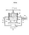
- FIG. 3is a cross sectional view of an exemplary substrate bonding apparatus according to the present invention.
- FIG. 4Ais an enlarged cross sectional view of region “A” of FIG. 3 according to the present invention.
- FIG. 4Bis an enlarged cross sectional view of region “B” of FIG. 3 according to the present invention.
- FIG. 4Cis an enlarged view of an exemplary alignment system and an upper stage of FIG. 3 according to the present invention.
- FIG. 4Dis a cross sectional view of another exemplary alignment system and an upper stage of FIG. 3 according to the present invention.
- FIG. 5Ais a cross sectional view taken along I—I of FIG. 3 according to the present invention.
- FIG. 5Bis a cross sectional view taken along II—II of FIG. 3 according to the present invention.
- FIG. 6is a cross sectional view of an exemplary alignment arrangement during an alignment process of the substrate bonding apparatus according to the present invention.
- FIG. 7is a cross sectional view of the exemplary bonding arrangement during a bonding process of the substrate bonding apparatus according to the present invention.
- FIG. 8Ais a cross sectional view of another exemplary substrate bonding apparatus during a first alignment process according to the present invention.
- FIG. 8Bis a cross sectional view of the exemplary substrate bonding apparatus during a second alignment process according to the present invention.
- FIG. 9Ais a cross sectional view taken along III—III of FIG. 8A according to the present invention.
- FIG. 9Bis a cross sectional view taken along IV—IV of FIG. 8A according to the present invention.
- FIG. 10Ashows an exemplary rough alignment process for aligning each substrate according to the present invention
- FIG. 10Bshows an exemplary process of controlling a rough focus of an alignment camera according to the present invention
- FIG. 10Cshows an exemplary fine alignment process for aligning each substrate according to the present invention
- FIG. 10Dshows another exemplary process of controlling a fine focus of an alignment camera according to the present invention.
- FIG. 11is a cross sectional view of another exemplary substrate bonding apparatus according to the present invention.
- FIG. 12is a cross sectional view taken along V—V of FIG. 11 according to the present invention.
- FIG. 13is a cross sectional view o taken along line VI—VI of FIG. 11 according to the present invention.
- FIG. 14is a cross sectional view of another exemplary substrate bonding apparatus according to the present invention.
- FIG. 15is a cross sectional view of another exemplary substrate bonding apparatus according to the present invention.
- FIG. 16is a cross sectional view taken along line VII—VII of FIG. 15 according to the present invention.
- FIG. 17is a cross sectional view taken along VII—VII of FIG. 15 according to the present invention.
- FIG. 18Ashows another exemplary process of aligning each substrate according to the present invention
- FIG. 18Bshows another exemplary process of controlling a focus of an alignment camera according to the present invention.
- FIG. 18Cshows another exemplary process of aligning each substrate according to the present invention.
- FIG. 18Dshows another exemplary process of controlling a focus of an alignment camera according to the present invention.
- FIG. 3is a cross sectional view of an exemplary substrate bonding apparatus according to the present invention
- FIGS. 4A and 4Bare enlarged cross sectional views of regions “A” and “B” of FIG. 3 according to the present invention
- the substrate bonding apparatusmay include a vacuum processing chamber 110 , an upper stage 121 , a lower stage 122 , a stage moving system, and a first alignment system 200 .
- the vacuum processing chamber 110may include a plurality of connecting holes 112 (in FIG. 4A ) positioned along uppermost surfaces of the vacuum processing chamber 110 .
- Each of the connecting holes 112may be aligned with alignment marks positioned on first and second substrates 510 and 520 .
- the upper stage 121may include a plurality of first through holes 121 a that may be aligned with the connecting holes 112 and with the alignment marks on the first and second substrates 510 and 520 .
- the first through holes 121 amay be formed at two or more opposite corners of the upper stage 121 .
- the first through holes 121 amay be formed at central portions of each edge of the upper stage 121 .
- the stage moving systemmay include an upper stage moving axis 131 that moves the upper stage 121 along an upward and downward direction, a lower stage moving axis 132 that rotates the lower stage 122 to left and right sides, and lower and upper stage driving motors 133 , 134 for driving the lower and upper stage moving axes 132 , 131 .
- the lower and upper stage driving motors 134 , 133may be provided at an exterior of the vacuum processing chamber 110 .
- lower and upper stage driving motors 134 , 133may be provided at an interior of the vacuum processing chamber 110 .
- the lower and upper stage driving motors 134 , 133may be provided at both an exterior and interior of the vacuum processing chamber 110 .
- the first alignment system 200may be provided with a first camera receiving portion 210 and a first align camera 220 , as shown in FIG. 4B .
- the first camera receiving portion 210may be formed of a tube shape, with a first end provided at the interior of the vacuum processing chamber 110 by passing through one of the connecting holes 112 .
- a spacemay be formed between sidewalls of the connecting hole 112 and a side of the first camera receiving portion 210 . Accordingly, a sealing process may be provided to prevent formation of the space.
- the first end of the first camera receiving portion 210is provided at the interior of the vacuum processing chamber 110 , whereby the alignment marks of the first and second substrates 510 and 520 may be observed through the first camera receiving portion 210 .
- a window 211may be provided at the first end of the first camera receiving portion 210 .
- the window 211 and the first camera receiving portion 210may include a high strength glass material that is resistance to the reduced pressure of a vacuum state.
- the first end of the first camera receiving portion 210may be provided above the first through hole 121 a of the upper stage 121 in the interior of the vacuum processing chamber 110 .
- FIG. 4Cis an enlarged view of an exemplary alignment system and an upper stage of FIG. 3 according to the present invention.
- the first camera receiving portion 210may be positioned in various configurations to observe the alignment marks of the first and second substrates 510 and 520 .
- the first camera receiving portion 210may be formed of a length that does not pass through the upper stage 121 .
- an additional receiving groovemay be formed for receiving the first camera receiving portion 210 .
- a first portion of the upper stage 121may be removed for receiving the first camera receiving portion 210 , and the first alignment camera 220 may be provided inside the first camera receiving portion 210 to observe the alignment marks of the first and second substrates 510 and 520 , thereby assisting in alignment of the first and second substrates 510 and 520 .
- FIG. 4Dis a cross sectional view of another exemplary alignment system and an upper stage of FIG. 3 according to the present invention.
- a first end of the first camera receiving portion 210may be provided at a portion where the first through hole 121 a is provided in the upper stage 121 .
- the first alignment camera 220may be inserted into the first camera receiving portion 210 so that the first alignment camera 220 travels with the movement of the first camera receiving portion 210 .
- a vacuum generating system 300may be provided for reducing the pressure of the interior of the vacuum processing chamber 110 .
- the first end of the first camera receiving portion 210may be connected to the upper stage moving axis 131 by a screw to travel along the upward and downward movement of the upper stage 121 when the upper stage moving axis 131 rotates.
- the first camera receiving portion 210(in FIGS. 4A–4D ) may be fixed to the vacuum chamber 110 , and may be connected to the first end of the first align camera 220 (in FIGS. 4A–4D ) with the upper stage moving axis 131 . Accordingly, the first align camera 220 moves along the downward and upward direction inside of the first camera receiving portion 210 according to the movement of the upper stage moving axis 131 .
- FIG. 5Ais a cross sectional view taken along I—I of FIG. 3 according to the present invention
- FIG. 5Bis a cross sectional view taken along II—II of FIG. 3 according to the present invention
- FIG. 6is a cross sectional view of an exemplary alignment arrangement during an alignment process of the substrate bonding apparatus according to the present invention.
- first and second substrates 510 and 520may be loaded onto lower and upper stages 122 and 121 , respectively.
- a vacuum processing chamber door 113may be operated to close an chamber entrance 111 of the vacuum processing chamber 110 , thereby sealing an interior of the vacuum processing chamber 110 .
- a vacuum generating system 300may be enabled to reduce a pressure in the interior of the vacuum processing chamber 110 , thereby creating a vacuum state within the interior of the vacuum processing chamber 110 .
- an upper stage driving motor 133 of the stage moving systemmay be driven so that the upper stage moving axis 131 rotates.
- the upper stage 121travels along a downward direction to a first location adjacent to the lower stage 122 .
- the first camera receiving portion 210 of the first alignment system 200travels along the downward according to the rotation of the upper stage moving axis 131 , so that a lower end (i.e., lens) of the first align camera 220 is positioned at a minimum distance from the substrate 510 that is provided on an upper surface of the lower stage 122 .
- the first alignment camera 220Upon completion of the alignment process, the first alignment camera 220 (in FIGS. 4A–4D ) checks alignment marks 511 and 521 (in FIGS. 5A and 5B ) of the first and second substrates 510 and 520 that are affixed to the lower and upper stages 122 and 121 , respectively. Accordingly, the first alignment camera 220 (in FIGS. 4A–4D ) may be focused onto a center point between the alignment marks 511 and 521 to check the alignment state of the first and second substrates 510 and 520 . Then, alignment data may be read from the first alignment camera 220 (in FIGS. 4A–4D ). Alternatively, the first alignment camera 220 (in FIGS.
- the stage moving systemmay be controlled by the alignment data, thereby aligning each substrate along a X-direction, a Y-direction, and rotating angles about a central axis.
- FIG. 7is a cross sectional view of the exemplary bonding arrangement during a bonding process of the substrate bonding apparatus according to the present invention.
- the stage moving systemmay be driven by a driving signal to bond the first and second substrates 510 and 520 together.
- FIG. 8Ais a cross sectional view of another exemplary substrate bonding apparatus during a first alignment process according to the present invention
- FIG. 8Bis a cross sectional view of the exemplary substrate bonding apparatus during a second alignment process according to the present invention
- a second alignment camera 420 of a second alignment system 400may form a pair with the first align camera 220 (in FIGS. 4A–4D ) for aligning a predetermined portion of the first and second substrates 510 and 520 .
- the second alignment system 400may be formed in the interior or exterior of the vacuum processing chamber 110 .
- the first alignment system 200is designed to align the first and second substrates 510 and 520 more precisely as compared with the second alignment system 400 , then the first alignment camera 220 of the first alignment system 200 may be provided in the interior of the vacuum processing chamber 110 , and the second alignment camera 420 may be provided in the exterior of the vacuum processing chamber 110 . That is, the first alignment system 200 may be provided at a minimum distance from the alignment marks 511 and 521 of the first and second substrates 510 and 520 , and the second alignment system may support the first alignment system 200 to precisely align the first and second substrates 510 and 520 .
- each of the first and second alignment cameras 220 (in FIGS. 4A–4D ) and 420face to four corners of each of the first and second substrates 510 and 520 to precisely align each of the first and second substrates 510 and 520 .
- the first and second alignment cameras 220 (in FIGS. 4A–4D ) and 420may face to each central point of four edges of each of the first and second substrates 510 and 520 .
- the first and second alignment cameras 220 (in FIGS. 4A–4D ) and 420may face two corners of each of the first and second substrates 510 and 520 .
- first and second alignment cameras 220in FIGS. 4A–4D ) and 420 may face other portions of the first and second substrates 510 and 520 , such as portions of dummy regions of the first and second substrates 510 and 520 .
- FIG. 9Ais a cross sectional view taken along III—III of FIG. 8A according to the present invention
- FIG. 9Bis a cross sectional view taken along IV—IV of FIG. 8A according to the present invention.
- the second substrate 520may have a second set of alignment marks 521 and 522
- the first substrate 510may have a first set of alignment marks 511 and 512 .
- the first through holes 121 a and a plurality of second through holes 121 b formed in the upper stage 121 and 121 bmay be aligned with the alignment marks 511 , 521 , 512 , 522 of the first and second substrates 510 and 520 .
- the first alignment cameras 220may be aligned with each of the first through holes 121 a for checking the alignment state of the first and second substrates 510 and 520 via a “rough” alignment mark 522 of the second substrate 520 and a “rough” alignment mark 512 of the first substrate 510 .
- the second alignment cameras 420(in FIG. 8A ) may be aligned with each of the second through holes 121 b for checking the alignment state of the first and second substrates 510 and 520 via a “fine” alignment mark 521 of the second substrate 520 and a “fine” alignment mark 511 of the first substrate 510 .
- Exemplary processing steps for aligning the first and second substrates 510 and 520 in the substrate bonding apparatus according to the present inventionwill be explained with regard to FIGS. 8A , 8 B, 9 A, and 9 B.
- the individual process steps for loading each of the first and second substrates 510 and 520 , and generating the vacuum state in the interior of the vacuum processing chamber 110may be the same as the individual process steps previously described with respect to FIGS. 5A , 5 B, and 6 .
- the upper stage driving motor 133 of the stage moving systemis driven so that the upper stage moving axis 131 rotates, thereby moving the upper stage 121 along a downward direction, as shown in FIG. 8B .
- the upper stage driving motor 133is disabled.
- the first and second substrates 510 and 520may be first aligned by the second alignment cameras 420 of the second alignment system 400 . That is, the second alignment cameras 420 may check the “rough” alignment marks 512 and 522 of each of the first and second substrates 510 and 520 .
- the second align camera 420may check whether the “rough” alignment marks 512 and 522 are within a visual range of the second align camera 420 . Accordingly, the second alignment cameras 420 may be focused on the central portion between the first and second substrates 510 and 520 to check the location of the first and second substrates 510 and 520 . Thus, each of the first and second substrates 510 and 520 may be first aligned according to the alignment process step. Next, the “fine” alignment marks 511 and 521 of the first and second substrates 510 and 520 may be positioned within the visual range of the first alignment cameras 220 (in FIGS. 4A–4D ). Then, the first and second substrates 510 and 520 may be aligned by the first alignment cameras 220 (in FIGS. 4A–4D ). Thus, the process step for aligning the first and second substrates 510 and 520 may be performed efficiently and easily.
- the first camera receiving portion 210 (in FIGS. 4A–4D ) of the first align camera 220 (in FIGS. 4A–4D )may travel along the downward direction along with the upper stage 121 , and the lower end (i.e., lens) of the first alignment camera 220 (in FIGS. 4A–4D ) may be provided at the minimum distance from each of the first and second substrates 510 and 520 .
- the first alignment camera 220(in FIGS. 4A–4D ) may check the location of each “fine” alignment mark 511 and 521 of both the first and second substrates 510 and 520 to precisely align each of the first and second substrates 510 and 520 .
- the “fine” alignment marks 511 and 521may be positioned within the visual range of the first alignment cameras 220 (in FIGS. 4A–4D ) after the first alignment of the first and second substrates 510 and 520 , the “fine” alignment marks 511 and 521 may be easily and quickly checked by the first alignment cameras 220 (in FIGS. 4A–4D ).
- FIG. 10Ashows an exemplary rough alignment process for aligning each substrate according to the present invention
- FIG. 10Bshows an exemplary process of controlling a rough focus of an alignment camera according to the present invention
- the first alignment cameras 220may be focused on the “rough” align mark 522 of the second substrate 520 affixed to the upper stage 121 , thereby checking the location of the second substrate 520 .
- the first alignment cameras 220may be focused on the “rough” alignment marks 512 of the first substrate 510 affixed to the lower stage 122 to check the location of the lower substrate 510 .
- a deflection valuemay be read with respect to a location between the “rough” alignment marks 512 and 522 , and then a displacement value may be calculated using the deflection value, thereby moving the upper stage 121 (in FIG. 8A ), or the lower stage according to the calculated displacement.
- the first and second substrates 510 and 520may be aligned.
- FIG. 10Cshows an exemplary fine alignment process for aligning each substrate according to the present invention
- FIG. 10Dshows an exemplary process of controlling a fine focus of an alignment camera according to the present invention
- the second alignment cameras 420may be focused on the “fine” align mark 521 of the second substrate 520 affixed to the upper stage 121 , thereby checking the location of the second substrate 520 .
- the second alignment cameras 420may be focused on the “fine” alignment mark 511 of the first substrate 510 affixed to the lower stage 122 to check the location of the lower substrate 510 .
- a deflection valuemay be read with respect to a location between the “fine” alignment marks 511 and 521 , and then a displacement value may be calculated using the deflection value, thereby moving the upper stage 121 , or the lower stage according to the calculated displacement.
- the first and second substrates 510 and 520may be aligned.
- the stage moving systemmay be successively driven by the driving signal, and then the second substrate 520 affixed to the upper stage 121 may be bonded to the first substrate 510 affixed to the lower stage 122 by pressing.
- the first and second alignment cameras 220 and 420may be formed in the interior of the vacuum chamber 110 , or on the exterior of the vacuum chamber 110 .
- each of the first and the second alignment systems 200 and 400may have two alignment cameras, or four alignment cameras.
- each of the first and second substrates 510 and 520may be aligned by checking each of the “fine” alignment marks 511 and 521 positioned on the first and second substrates 510 and 520 , or by checking a center point between the “fine” alignment marks 511 and 521 of each of the first and second substrates 510 and 520 , or respectively checking the “fine” alignment marks 511 and 521 of each of the first and second substrates 510 and 520 with the first alignment system 200 , and at the same time, reading the location value of the center point between the “fine” alignment marks 511 and 521 of each of the first and second substrates 510 and 520 .
- FIG. 11is a cross sectional view of another exemplary substrate bonding apparatus according to the present invention
- FIG. 12is a cross sectional view taken along V—V of FIG. 11 according to the present invention
- FIG. 13is a cross sectional view taken along line VI—VI of FIG. 11 according to the present invention.
- a plurality of through holes 113may be provided at a bottom of the vacuum processing chamber 110
- a third alignment system 600may be provided below the vacuum processing chamber 600 . Accordingly, a total number of the through holes 113 may be the same as a total number of “rough” and “fine” alignment marks of the first and second substrates 510 and 520 .
- a plurality of third through holes 122 amay be formed in a lower stage 122 , which may be aligned to each of the through holes 113 provided at the bottom of the vacuum chamber 110 to check each of the “fine” alignment marks 511 and 521 .
- the third alignment system 600may be provided below the vacuum processing chamber 110 to be aligned to the “fine” alignment marks 511 and 521 of the first and second substrates 510 and 520 , so that the third alignment system 600 can check the “fine” alignment marks 511 and 521 of the first and second substrates 510 and 520 through the through holes 113 of the vacuum processing chamber 110 and the third through holes 122 a of the lower stage 220 , thereby aligning each of the first and second substrates 510 and 520 .
- the third alignment system 600may include a plurality of alignment cameras for checking the alignment marks of the first and second substrates 510 and 520 and for checking the alignment state between the first and second substrates 510 and 520 .
- a total number of the third alignment systems 600directly corresponds to a total number of the third through holes 122 a.
- FIGS. 11 , 12 , and 13Exemplary processing steps for aligning substrates in the substrate bonding apparatus according to the present invention will be explained with regard to FIGS. 11 , 12 , and 13 .
- the first and second substrates 510 and 520may be loaded onto the lower and upper stages 122 and 121 , respectively, and the vacuum chamber 110 may be sealed.
- the pressure in the interior of the vacuum processing chamber 110may be reduced by a vacuum generating system 300 , until the interior of the vacuum processing chamber 110 reaches the vacuum state.
- the upper stage 121may travel along a downward direction by enabling the stage moving system, and becomes positioned adjacent to the lower stage 122 .
- the third alignment cameras 600may check each alignment mark 511 provided on the lower substrate 510 affixed to the lower stage 122 (in FIG. 13 ), and each alignment mark 521 provided on the upper substrate 520 affixed to the upper stage 121 (in FIG. 12 ), thereby checking the location of the first and second substrates 510 and 520 .
- the third alignment system 122may be focused upon a center point between the alignment marks 511 and 521 , and may be alternately focused on each alignment mark 511 and 521 , thereby checking the location of the first and second substrates 510 and 520 .
- the stage moving systemmay be controlled by reading data relating to the alignment state of the first and second substrates 510 and 520 . Accordingly, each of the first and second substrates 510 and 520 may be aligned with respect to X-direction, Y-direction, and opposing angles.
- FIG. 14is a cross sectional view of another exemplary substrate bonding apparatus according to the present invention.
- the third alignment system 600may be provided in the lower part of the vacuum chamber 110 . Accordingly, a first end of the third alignment system 600 may be provided in the interior of the vacuum processing chamber 110 for being close to the alignment marks, thereby improving accuracy in checking the location of the first and second substrates 510 and 520 , and reading the location data.
- the vacuum processing chamber 110may further include a third camera receiving portion 610 for receiving the first end of the third alignment system 600 .
- the third camera receiving portion 610may include a transparent material to protect the third alignment system 600 under the vacuum state.
- FIG. 15is a cross sectional view of another exemplary substrate bonding apparatus according to the present invention
- FIG. 16is a cross sectional view taken along line VII—VII of FIG. 15 according to the present invention
- FIG. 17is a cross sectional view taken along VIII—VIII of FIG. 15 according to the present invention.
- an fourth alignment system 700may include fourth alignment cameras paired with the third alignment system 600 having the third alignment cameras in order to align each substrate by checking each alignment mark of the substrates.
- the third alignment system 700may be provided to align the location of the first and second substrates 510 and 520 more precisely, and the fourth alignment system 700 may be provided to support the third alignment system 600 for aligning the first and second substrates 510 and 520 . Accordingly, the third alignment system 600 may be provided at the minimum distance from the alignment marks 511 and 521 of the first and second substrates 510 and 520 .
- the fourth alignment system 700may be provided above the vacuum processing chamber 110 to align the first and second substrates 510 and 520 via a plurality of through holes 114 .
- the fourth alignment system 700checks “rough” alignment marks 511 a and 521 a of the first and second substrates 510 and 520 (in FIGS. 17 and 18 ), and the third alignment system 600 checks “fine” alignment marks 511 b and 521 b of the first and second substrates 510 and 520 .
- the fourth alignment system 700approximately aligns the first and second substrates 510 and 520 via the “rough” alignment marks 511 a and 521 a
- the third alignment system 600precisely aligns the first and second substrates 510 and 520 via the “fine” align marks 511 b and 521 b.
- the fourth alignment system 700may be provided at a portion relatively close to the third alignment system 600 below the vacuum processing chamber 110 .
- the fourth alignment system 700since a space below the vacuum chamber 110 is generally small, and the fourth alignment system 700 does not require high accuracy, it may be preferable to provide the fourth alignment system 700 above the vacuum chamber 110 .
- each substratemay be aligned in the same way as the alignment process of FIGS. 11 , 12 , and 13 .
- the fourth alignment system 700may approximately align the first and second substrates 510 and 520
- the third alignment system 600may precisely align the first and second substrates 510 and 520 . That is, the fourth alignment system 700 first checks the “rough” alignment marks 511 and 521 of the first and second substrates 510 and 520 , as shown in FIGS. 16 and 17 , via first through holes 114 provided at the top of the vacuum processing chamber 110 and fourth through holes 121 c provided in the upper stage 121 .
- the fourth alignment system 700checks whether the “rough” alignment marks 511 a and 521 a are within the visual range of the fourth alignment system 700 . Accordingly, the fourth alignment system 700 may be focused on a center point between the first and second substrates 510 and 520 to check the location of the substrates, as shown in FIG. 18B .
- the “fine” alignment marks 511 b and 521 b of the first and second substrates 510 and 520are first aligned for being positioned within the visual range of the third alignment system 600 , thereby quickly and easily aligning the first and second substrates 510 and 520 at a high accuracy. If the “rough” alignment marks 511 a and 521 a of the first and second substrates 510 are 520 are positioned within the visual range of the fourth alignment system 700 , the third alignment system 600 performs a second alignment of the first and second substrates 510 and 520 .
- the third alignment system 600checks the “fine” alignment marks 511 b and 521 b of the first and second substrates 510 and 520 through the third through holes 122 a provided in the lower stage 122 , and precisely aligns the location of the first and second substrates 510 and 520 . Since the “fine” alignment marks 511 b and 521 b are already positioned within the visual range of the third alignment system 600 , the third alignment system 600 checks the location of the first and second substrates 510 and 520 more easily and exactly.
- the first and second substrates 510 and 520may be aligned by the third alignment system 600 in the following method.
- the third alignment system 600may be focused on the “fine” alignment mark 521 b of the second substrate 520 affixed to the upper stage 121 to check the location of the second substrate 520 .
- the third alignment system 600may be focused on the “fine” alignment mark 511 b of the first substrate 510 affixed to the lower stage 122 to check the location of the first substrate 510 , as shown in FIGS. 18C and 18D .
- a deflection valuemay be read according to the location between the “fine” alignment marks 511 b and 521 b .
- a displacementmay be calculated using the deflection value, thereby moving the upper stage 121 , or the lower stage 122 according to the calculated displacement. Accordingly, the first and second substrates 510 and 520 may be precisely aligned.
Landscapes
- Liquid Crystal (AREA)
- Container, Conveyance, Adherence, Positioning, Of Wafer (AREA)
Abstract
Description
Claims (9)
Priority Applications (1)
| Application Number | Priority Date | Filing Date | Title |
|---|---|---|---|
| US11/043,042US7250989B2 (en) | 2002-03-15 | 2005-01-27 | Substrate bonding apparatus having alignment system with one end provided inside vacuum chamber for liquid crystal display device |
Applications Claiming Priority (6)
| Application Number | Priority Date | Filing Date | Title |
|---|---|---|---|
| KR1020020014182AKR100710156B1 (en) | 2002-03-15 | 2002-03-15 | bonding device for liquid crystal display device |
| KRP2002-14182 | 2002-03-15 | ||
| KR1020020015953AKR100685922B1 (en) | 2002-03-25 | 2002-03-25 | Bonding device for liquid crystal display device |
| KRP2002-15953 | 2002-03-25 | ||
| US10/259,439US6885427B2 (en) | 2002-03-15 | 2002-09-30 | Substrate bonding apparatus for liquid crystal display device having alignment system with one end provided inside vacuum chamber |
| US11/043,042US7250989B2 (en) | 2002-03-15 | 2005-01-27 | Substrate bonding apparatus having alignment system with one end provided inside vacuum chamber for liquid crystal display device |
Related Parent Applications (1)
| Application Number | Title | Priority Date | Filing Date |
|---|---|---|---|
| US10/259,439DivisionUS6885427B2 (en) | 2002-03-15 | 2002-09-30 | Substrate bonding apparatus for liquid crystal display device having alignment system with one end provided inside vacuum chamber |
Publications (2)
| Publication Number | Publication Date |
|---|---|
| US20050128422A1 US20050128422A1 (en) | 2005-06-16 |
| US7250989B2true US7250989B2 (en) | 2007-07-31 |
Family
ID=28043911
Family Applications (2)
| Application Number | Title | Priority Date | Filing Date |
|---|---|---|---|
| US10/259,439Expired - LifetimeUS6885427B2 (en) | 2002-03-15 | 2002-09-30 | Substrate bonding apparatus for liquid crystal display device having alignment system with one end provided inside vacuum chamber |
| US11/043,042Expired - LifetimeUS7250989B2 (en) | 2002-03-15 | 2005-01-27 | Substrate bonding apparatus having alignment system with one end provided inside vacuum chamber for liquid crystal display device |
Family Applications Before (1)
| Application Number | Title | Priority Date | Filing Date |
|---|---|---|---|
| US10/259,439Expired - LifetimeUS6885427B2 (en) | 2002-03-15 | 2002-09-30 | Substrate bonding apparatus for liquid crystal display device having alignment system with one end provided inside vacuum chamber |
Country Status (3)
| Country | Link |
|---|---|
| US (2) | US6885427B2 (en) |
| JP (1) | JP4024698B2 (en) |
| CN (1) | CN1315001C (en) |
Families Citing this family (25)
| Publication number | Priority date | Publication date | Assignee | Title |
|---|---|---|---|---|
| FR2796491B1 (en)* | 1999-07-12 | 2001-08-31 | Commissariat Energie Atomique | METHOD FOR TAKING OFF TWO ELEMENTS AND DEVICE FOR IMPLEMENTING SAME |
| KR100542224B1 (en)* | 2003-10-09 | 2006-01-11 | 삼성에스디아이 주식회사 | Plasma display device, method for manufacturing same, and manufacturing device |
| TWI275868B (en)* | 2003-11-24 | 2007-03-11 | Advanced Display Proc Eng Co | Substrate combining device and method |
| US8146641B2 (en)* | 2003-12-01 | 2012-04-03 | Lg Display Co., Ltd. | Sealant hardening apparatus of liquid crystal display panel and sealant hardening method thereof |
| KR101010450B1 (en)* | 2003-12-17 | 2011-01-21 | 엘지디스플레이 주식회사 | LCD Dropping Device |
| JP4190472B2 (en)* | 2004-07-28 | 2008-12-03 | シャープ株式会社 | Manufacturing method and manufacturing apparatus of liquid crystal display element |
| JP4751612B2 (en)* | 2004-12-28 | 2011-08-17 | 芝浦メカトロニクス株式会社 | Substrate bonding apparatus and substrate bonding method |
| KR100696623B1 (en)* | 2005-01-20 | 2007-03-19 | 삼성에스디아이 주식회사 | Plasma display device and manufacturing method thereof |
| KR100928494B1 (en)* | 2005-04-15 | 2009-11-26 | 엘지디스플레이 주식회사 | LCD and its manufacturing method |
| JP4078487B2 (en)* | 2005-05-25 | 2008-04-23 | 株式会社日立プラントテクノロジー | Substrate assembly apparatus and method |
| KR20070005368A (en)* | 2005-07-06 | 2007-01-10 | 삼성에스디아이 주식회사 | Plasma display panel |
| US7462280B2 (en)* | 2005-07-22 | 2008-12-09 | Agilent Technologies, Inc. | Liquid chromatography chip with flexible interface |
| KR100688830B1 (en)* | 2005-09-20 | 2007-03-02 | 삼성에스디아이 주식회사 | Method for manufacturing organic light emitting display device and apparatus for manufacturing same |
| KR101116322B1 (en)* | 2009-08-17 | 2012-03-09 | 에이피시스템 주식회사 | Method of aligning substrate |
| CN102004347B (en)* | 2009-09-02 | 2013-03-20 | 北京京东方光电科技有限公司 | Liquid crystal display and substrate |
| KR101646783B1 (en)* | 2009-12-08 | 2016-08-08 | 엘지디스플레이 주식회사 | Portable computer |
| JP4955807B1 (en)* | 2010-12-15 | 2012-06-20 | パナソニック株式会社 | Manufacturing method of semi-finished blank for variable focus lens |
| CN102299089A (en)* | 2011-08-01 | 2011-12-28 | 海尔集团公司 | Bonding platform |
| KR101394312B1 (en)* | 2012-11-07 | 2014-05-13 | 주식회사 신성에프에이 | Wafer alignment apparatus |
| CN103293740B (en)* | 2013-03-29 | 2016-04-27 | 深超光电(深圳)有限公司 | Liquid crystal display panel |
| JP6311967B2 (en)* | 2014-03-06 | 2018-04-18 | Tianma Japan株式会社 | Substrate bonding apparatus and substrate bonding method |
| CN104821377B (en)* | 2015-05-05 | 2017-07-21 | 合肥京东方光电科技有限公司 | Paster packaging system and method |
| CN110154405A (en)* | 2018-02-02 | 2019-08-23 | 深圳市义鹏技术有限公司 | Vacuum abutted jig and its applying method for 3D bend glass and rupture pressure disc |
| KR102161093B1 (en)* | 2018-12-14 | 2020-09-29 | 주식회사 엘트린 | Substrate bonding apparatus |
| KR20250019196A (en)* | 2023-07-31 | 2025-02-10 | 삼성디스플레이 주식회사 | Method of manufacturing display device |
Citations (235)
| Publication number | Priority date | Publication date | Assignee | Title |
|---|---|---|---|---|
| JPS5165656A (en) | 1974-12-04 | 1976-06-07 | Shinshu Seiki Kk | |
| US3978580A (en) | 1973-06-28 | 1976-09-07 | Hughes Aircraft Company | Method of fabricating a liquid crystal display |
| JPS52149725A (en) | 1976-06-07 | 1977-12-13 | Ichikoh Ind Ltd | Non contact system lamp checker for vehicle |
| US4094058A (en) | 1976-07-23 | 1978-06-13 | Omron Tateisi Electronics Co. | Method of manufacture of liquid crystal displays |
| JPS5738414A (en) | 1980-08-20 | 1982-03-03 | Showa Denko Kk | Spacer for display panel |
| JPS5788428A (en) | 1980-11-20 | 1982-06-02 | Ricoh Elemex Corp | Manufacture of liquid crystal display body device |
| JPS5827126A (en) | 1981-08-11 | 1983-02-17 | Nec Corp | Production of liquid crystal display panel |
| JPS5957221A (en) | 1982-09-28 | 1984-04-02 | Asahi Glass Co Ltd | Production of display element |
| JPS59195222A (en) | 1983-04-19 | 1984-11-06 | Matsushita Electric Ind Co Ltd | Manufacture of liquid-crystal panel |
| JPS60111221A (en) | 1983-11-19 | 1985-06-17 | Nippon Denso Co Ltd | Method and device for charging liquid crystal |
| JPS60164723A (en) | 1984-02-07 | 1985-08-27 | Seiko Instr & Electronics Ltd | Liquid crystal display device |
| JPS60217343A (en) | 1984-04-13 | 1985-10-30 | Matsushita Electric Ind Co Ltd | Liquid crystal display device and its preparation |
| JPS617822A (en) | 1984-06-22 | 1986-01-14 | Canon Inc | Production of liquid crystal element |
| JPS6155625A (en) | 1984-08-24 | 1986-03-20 | Nippon Denso Co Ltd | Manufacture of liquid crystal element |
| JPS6254225A (en) | 1985-07-15 | 1987-03-09 | Semiconductor Energy Lab Co Ltd | Manufacturing method for liquid crystal display |
| JPS6254228A (en) | 1985-07-15 | 1987-03-09 | Semiconductor Energy Lab Co Ltd | Manufacturing method for liquid crystal display |
| JPS6254229A (en) | 1985-07-15 | 1987-03-09 | Semiconductor Energy Lab Co Ltd | Manufacturing method for liquid crystal display |
| US4653864A (en) | 1986-02-26 | 1987-03-31 | Ovonic Imaging Systems, Inc. | Liquid crystal matrix display having improved spacers and method of making same |
| JPS6289025A (en) | 1985-10-15 | 1987-04-23 | Matsushita Electric Ind Co Ltd | Manufacturing method of liquid crystal display panel |
| JPS6290622A (en) | 1985-10-17 | 1987-04-25 | Seiko Epson Corp | liquid crystal display device |
| US4691995A (en) | 1985-07-15 | 1987-09-08 | Semiconductor Energy Laboratory Co., Ltd. | Liquid crystal filling device |
| JPS62205319A (en) | 1986-03-06 | 1987-09-09 | Canon Inc | Ferroelectric liquid crystal element |
| JPS63110425A (en) | 1986-10-29 | 1988-05-14 | Toppan Printing Co Ltd | Cell for liquid crystal filling |
| JPS63109413A (en) | 1986-10-27 | 1988-05-14 | Fujitsu Ltd | Manufacturing method of LCD display |
| JPS63128315A (en) | 1986-11-19 | 1988-05-31 | Victor Co Of Japan Ltd | Liquid crystal display element |
| US4775225A (en) | 1985-05-16 | 1988-10-04 | Canon Kabushiki Kaisha | Liquid crystal device having pillar spacers with small base periphery width in direction perpendicular to orientation treatment |
| JPS63311233A (en) | 1987-06-12 | 1988-12-20 | Toyota Motor Corp | lcd cell |
| JPH039549A (en) | 1989-05-16 | 1991-01-17 | Motorola Inc | Composite integrated storage device |
| JPH0536426A (en) | 1991-07-31 | 1993-02-12 | Mitsubishi Heavy Ind Ltd | Solid electrolytic fuel cell |
| JPH0536425A (en) | 1991-02-12 | 1993-02-12 | Tokyo Electric Power Co Inc:The | Alloy separator for solid oxide fuel cell and method for producing the same |
| JPH05107533A (en) | 1991-10-16 | 1993-04-30 | Shinetsu Eng Kk | Method for laminating glass substrate for liquid crystal display panel and laminating apparatus therefor |
| JPH05127179A (en) | 1991-11-01 | 1993-05-25 | Ricoh Co Ltd | Production of liquid crystal display element |
| JPH05143923A (en) | 1991-11-25 | 1993-06-11 | Matsushita Electric Ind Co Ltd | Magnetic head manufacturing method |
| JPH05154923A (en) | 1991-12-06 | 1993-06-22 | Hitachi Ltd | Substrate assembling device |
| US5222293A (en) | 1992-04-23 | 1993-06-29 | Eastman Kodak Company | System for placing an object on a carrier and method |
| US5247377A (en) | 1988-07-23 | 1993-09-21 | Rohm Gmbh Chemische Fabrik | Process for producing anisotropic liquid crystal layers on a substrate |
| JPH05265011A (en) | 1992-03-19 | 1993-10-15 | Seiko Instr Inc | Production of liquid crystal display element |
| JPH05281562A (en) | 1992-04-01 | 1993-10-29 | Matsushita Electric Ind Co Ltd | Manufacture of liquid crystal panel |
| JPH05281557A (en) | 1992-04-01 | 1993-10-29 | Matsushita Electric Ind Co Ltd | Liquid crystal panel manufacturing method |
| US5263888A (en) | 1992-02-20 | 1993-11-23 | Matsushita Electric Industrial Co., Ltd. | Method of manufacture of liquid crystal display panel |
| JPH0618829A (en) | 1992-06-30 | 1994-01-28 | Shinetsu Eng Kk | Device for laminating glass substrates for liquid crystal display boards |
| JPH0651256A (en) | 1992-07-30 | 1994-02-25 | Matsushita Electric Ind Co Ltd | Device for discharging liquid crystal |
| JPH0664229A (en) | 1992-08-24 | 1994-03-08 | Toshiba Corp | Optical printing head |
| JPH06148657A (en) | 1992-11-06 | 1994-05-27 | Matsushita Electric Ind Co Ltd | Method of manufacturing cell for liquid crystal display and manufacturing apparatus thereof |
| JPH06160871A (en) | 1992-11-26 | 1994-06-07 | Matsushita Electric Ind Co Ltd | Liquid crystal display panel and manufacturing method thereof |
| JPH06194637A (en) | 1992-12-24 | 1994-07-15 | Shinetsu Eng Kk | Method for sticking glass substrate for liquid crystal display plate |
| JPH06235925A (en) | 1993-02-10 | 1994-08-23 | Matsushita Electric Ind Co Ltd | Manufacture of liquid crystal display element |
| JPH06265915A (en) | 1993-03-12 | 1994-09-22 | Matsushita Electric Ind Co Ltd | Discharge device for filling liquid crystal |
| JPH06313870A (en) | 1993-04-28 | 1994-11-08 | Hitachi Ltd | Substrate assembly device |
| US5379139A (en) | 1986-08-20 | 1995-01-03 | Semiconductor Energy Laboratory Co., Ltd. | Liquid crystal device and method for manufacturing same with spacers formed by photolithography |
| JPH0784268A (en) | 1993-09-13 | 1995-03-31 | Hitachi Ltd | Sealing agent drawing method |
| US5406989A (en) | 1993-10-12 | 1995-04-18 | Ayumi Industry Co., Ltd. | Method and dispenser for filling liquid crystal into LCD cell |
| JPH07128674A (en) | 1993-11-05 | 1995-05-19 | Matsushita Electric Ind Co Ltd | Liquid crystal display element manufacturing method |
| JPH07181507A (en) | 1993-12-21 | 1995-07-21 | Canon Inc | Liquid crystal display device and information transmission device including the liquid crystal display device |
| JPH07275770A (en) | 1994-04-06 | 1995-10-24 | Hitachi Techno Eng Co Ltd | Paste applicator |
| JPH07275771A (en) | 1994-04-11 | 1995-10-24 | Hitachi Techno Eng Co Ltd | Paste applicator |
| US5499128A (en) | 1993-03-15 | 1996-03-12 | Kabushiki Kaisha Toshiba | Liquid crystal display device with acrylic polymer spacers and method of manufacturing the same |
| JPH0876133A (en) | 1994-09-02 | 1996-03-22 | Shinetsu Eng Kk | Surface plate structure in a bonding apparatus for glass substrates for liquid crystal display boards |
| JPH0895066A (en) | 1994-09-27 | 1996-04-12 | Matsushita Electric Ind Co Ltd | Method and apparatus for manufacturing liquid crystal element |
| US5507323A (en) | 1993-10-12 | 1996-04-16 | Fujitsu Limited | Method and dispenser for filling liquid crystal into LCD cell |
| JPH08101395A (en) | 1994-09-30 | 1996-04-16 | Matsushita Electric Ind Co Ltd | Liquid crystal display element manufacturing method |
| JPH08106101A (en) | 1994-10-06 | 1996-04-23 | Fujitsu Ltd | Liquid crystal display panel manufacturing method |
| JPH08110504A (en) | 1994-10-13 | 1996-04-30 | Shinetsu Eng Kk | Glass substrate heating device for liquid crystal display panel |
| JPH08136937A (en) | 1994-11-09 | 1996-05-31 | Shinetsu Eng Kk | Method and apparatus for pressurizing and heating glass substrate for liquid crystal display panel |
| JPH08171094A (en) | 1994-12-19 | 1996-07-02 | Nippon Soken Inc | Liquid crystal injecting method and liquid crystal injecting device to liquid crystal display device |
| JPH08173874A (en) | 1994-12-26 | 1996-07-09 | Hitachi Techno Eng Co Ltd | Paste applicator |
| JPH08190099A (en) | 1995-01-11 | 1996-07-23 | Fujitsu Ltd | Liquid crystal display device manufacturing method and liquid crystal display device manufacturing apparatus |
| US5539545A (en) | 1993-05-18 | 1996-07-23 | Semiconductor Energy Laboratory Co., Ltd. | Method of making LCD in which resin columns are cured and the liquid crystal is reoriented |
| US5548429A (en) | 1993-06-14 | 1996-08-20 | Canon Kabushiki Kaisha | Process for producing liquid crystal device whereby curing the sealant takes place after pre-baking the substrates |
| JPH08240807A (en) | 1995-03-06 | 1996-09-17 | Fujitsu Ltd | Liquid crystal display panel sealing method |
| JPH091026A (en) | 1995-06-23 | 1997-01-07 | Hitachi Techno Eng Co Ltd | Paste applicator |
| JPH095762A (en) | 1995-06-20 | 1997-01-10 | Matsushita Electric Ind Co Ltd | Liquid crystal panel manufacturing method |
| JPH0926578A (en) | 1995-07-10 | 1997-01-28 | Fujitsu Ltd | Liquid crystal display panel and method of manufacturing the same |
| JPH0961829A (en) | 1995-08-21 | 1997-03-07 | Matsushita Electric Ind Co Ltd | Liquid crystal display element manufacturing method |
| JPH0973075A (en) | 1995-09-05 | 1997-03-18 | Matsushita Electric Ind Co Ltd | Liquid crystal display element manufacturing method and liquid crystal display element manufacturing apparatus |
| JPH0973096A (en) | 1995-09-05 | 1997-03-18 | Matsushita Electric Ind Co Ltd | Liquid crystal display element manufacturing method |
| JPH0994500A (en) | 1995-09-29 | 1997-04-08 | Hitachi Techno Eng Co Ltd | Paste applicator |
| JPH09127528A (en) | 1995-10-27 | 1997-05-16 | Fujitsu Ltd | Liquid crystal panel manufacturing method |
| US5642214A (en) | 1991-07-19 | 1997-06-24 | Sharp Kabushiki Kaisha | Optical modulating element and electronic apparatus using it |
| JPH09230357A (en) | 1996-02-22 | 1997-09-05 | Canon Inc | Liquid crystal panel manufacturing method and liquid crystal cell used therefor |
| JPH09281511A (en) | 1996-04-17 | 1997-10-31 | Fujitsu Ltd | Liquid crystal display panel manufacturing method |
| JPH09311340A (en) | 1996-05-21 | 1997-12-02 | Matsushita Electric Ind Co Ltd | Liquid crystal display manufacturing method |
| US5742370A (en) | 1996-09-12 | 1998-04-21 | Korea Institute Of Science And Technology | Fabrication method for liquid crystal alignment layer by magnetic field treatment |
| JPH10123538A (en) | 1996-10-22 | 1998-05-15 | Matsushita Electric Ind Co Ltd | Manufacturing method of liquid crystal display element |
| JPH10123537A (en) | 1996-10-15 | 1998-05-15 | Matsushita Electric Ind Co Ltd | Liquid crystal display device and method of manufacturing the same |
| US5757451A (en) | 1995-09-08 | 1998-05-26 | Kabushiki Kaisha Toshiba | Liquid crystal display device spacers formed from stacked color layers |
| JPH10142616A (en) | 1996-11-14 | 1998-05-29 | Ayumi Kogyo Kk | Liquid crystal injection method and liquid dispenser |
| JPH10174477A (en) | 1996-12-06 | 1998-06-26 | Hitachi Ltd | Electric motor drive device and air conditioner using the same |
| JPH10174924A (en) | 1996-12-17 | 1998-06-30 | Hitachi Techno Eng Co Ltd | Paste coating machine |
| JPH10177178A (en) | 1996-12-17 | 1998-06-30 | Matsushita Electric Ind Co Ltd | Manufacturing method of liquid crystal display element |
| US5783026A (en)* | 1995-05-24 | 1998-07-21 | International Business Machines Corporation | Apparatus for stacking sheets by carriers |
| JPH10221700A (en) | 1997-02-10 | 1998-08-21 | Fujitsu Ltd | Manufacturing method of liquid crystal display device |
| JPH10282512A (en) | 1997-04-07 | 1998-10-23 | Ayumi Kogyo Kk | Liquid crystal injection method and dispenser used therefor |
| JPH10333157A (en) | 1997-06-03 | 1998-12-18 | Matsushita Electric Ind Co Ltd | Manufacturing method of liquid crystal display device |
| JPH10333159A (en) | 1997-06-03 | 1998-12-18 | Matsushita Electric Ind Co Ltd | Liquid crystal display |
| US5852484A (en) | 1994-09-26 | 1998-12-22 | Matsushita Electric Industrial Co., Ltd. | Liquid crystal display panel and method and device for manufacturing the same |
| US5861932A (en) | 1997-03-31 | 1999-01-19 | Denso Corporation | Liquid crystal cell and its manufacturing method |
| JPH1114953A (en) | 1997-06-20 | 1999-01-22 | Matsushita Electric Ind Co Ltd | Method of manufacturing multi-touch liquid crystal display panel and multi-touch liquid crystal display panel |
| KR0156422B1 (en) | 1995-10-05 | 1999-02-01 | 김광호 | Reticle for manufacturing semiconductor device |
| JPH1138424A (en) | 1997-07-23 | 1999-02-12 | Fujitsu Ltd | Liquid crystal display panel and method of manufacturing the same |
| US5875922A (en) | 1997-10-10 | 1999-03-02 | Nordson Corporation | Apparatus for dispensing an adhesive |
| JPH1164811A (en) | 1997-08-21 | 1999-03-05 | Matsushita Electric Ind Co Ltd | Method and apparatus for manufacturing liquid crystal display element |
| JPH1188424A (en) | 1997-09-12 | 1999-03-30 | Nec Corp | Circular route simulation system |
| JPH11109388A (en) | 1997-10-03 | 1999-04-23 | Hitachi Ltd | Manufacturing method of liquid crystal display device |
| JPH11133438A (en) | 1997-10-24 | 1999-05-21 | Matsushita Electric Ind Co Ltd | Liquid crystal display device and its manufacturing method |
| JPH11142864A (en) | 1997-11-07 | 1999-05-28 | Matsushita Electric Ind Co Ltd | Manufacturing method of liquid crystal display device |
| JPH11174477A (en) | 1997-12-08 | 1999-07-02 | Matsushita Electric Ind Co Ltd | Manufacturing method of liquid crystal display device |
| JPH11212045A (en) | 1998-01-26 | 1999-08-06 | Matsushita Electric Ind Co Ltd | Liquid crystal panel manufacturing method |
| US5952676A (en) | 1986-08-20 | 1999-09-14 | Semiconductor Energy Laboratory Co., Ltd. | Liquid crystal device and method for manufacturing same with spacers formed by photolithography |
| JPH11248930A (en) | 1998-03-06 | 1999-09-17 | Matsushita Electric Ind Co Ltd | Color filter substrate, method of manufacturing the color filter substrate, and liquid crystal display device using the color filter substrate |
| US5956112A (en) | 1995-10-02 | 1999-09-21 | Sharp Kabushiki Kaisha | Liquid crystal display device and method for manufacturing the same |
| JPH11262712A (en) | 1998-03-17 | 1999-09-28 | Hitachi Techno Eng Co Ltd | Paste application method and paste application machine |
| JPH11264991A (en) | 1998-01-13 | 1999-09-28 | Matsushita Electric Ind Co Ltd | Manufacturing method of liquid crystal display element |
| JPH11281988A (en) | 1998-03-27 | 1999-10-15 | Matsushita Electric Ind Co Ltd | Manufacturing method of liquid crystal display element |
| JPH11326922A (en) | 1998-05-14 | 1999-11-26 | Matsushita Electric Ind Co Ltd | Liquid crystal display panel manufacturing method |
| US6001203A (en) | 1995-03-01 | 1999-12-14 | Matsushita Electric Industrial Co., Ltd. | Production process of liquid crystal display panel, seal material for liquid crystal cell and liquid crystal display |
| JPH11344714A (en) | 1998-06-02 | 1999-12-14 | Denso Corp | Liquid crystal cell |
| US6011609A (en) | 1996-10-05 | 2000-01-04 | Samsung Electronics Co., Ltd. | Method of manufacturing LCD by dropping liquid crystals on a substrate and then pressing the substrates |
| JP2000002879A (en) | 1998-06-12 | 2000-01-07 | Matsushita Electric Ind Co Ltd | Apparatus and method for assembling liquid crystal panel |
| US6016181A (en) | 1996-11-07 | 2000-01-18 | Sharp Kabushiki Kaisha | Liquid crystal device having column spacers with portion on each of the spacers for reflecting or absorbing visible light and method for fabricating the same |
| US6016178A (en) | 1996-09-13 | 2000-01-18 | Sony Corporation | Reflective guest-host liquid-crystal display device |
| JP2000029035A (en) | 1998-07-09 | 2000-01-28 | Minolta Co Ltd | Liquid crystal element and its manufacture |
| JP2000056311A (en) | 1998-08-03 | 2000-02-25 | Matsushita Electric Ind Co Ltd | Liquid crystal display |
| JP2000066165A (en) | 1998-08-20 | 2000-03-03 | Matsushita Electric Ind Co Ltd | Liquid crystal display panel manufacturing method |
| JP2000066218A (en) | 1998-08-21 | 2000-03-03 | Shinetsu Engineering Kk | LCD panel manufacturing equipment |
| US6036568A (en)* | 1997-06-04 | 2000-03-14 | Kabushiki Kaisha Toshiba | Method and apparatus for assembling liquid crystal display |
| JP2000093866A (en) | 1998-09-18 | 2000-04-04 | Hitachi Techno Eng Co Ltd | Paste application method and paste application machine |
| US6055035A (en) | 1998-05-11 | 2000-04-25 | International Business Machines Corporation | Method and apparatus for filling liquid crystal display (LCD) panels |
| JP2000137235A (en) | 1998-11-02 | 2000-05-16 | Matsushita Electric Ind Co Ltd | Liquid crystal substrate bonding method |
| EP1003066A1 (en) | 1998-11-16 | 2000-05-24 | Matsushita Electric Industrial Co., Ltd. | Method of manufacturing liquid crystal display devices |
| JP2000193988A (en) | 1998-12-25 | 2000-07-14 | Fujitsu Ltd | Method and apparatus for manufacturing liquid crystal display panel |
| JP2000241824A (en) | 1999-02-18 | 2000-09-08 | Matsushita Electric Ind Co Ltd | Manufacturing method of liquid crystal display device |
| JP2000284295A (en) | 1999-03-30 | 2000-10-13 | Hitachi Techno Eng Co Ltd | Substrate assembling method and apparatus |
| JP2000292799A (en) | 1999-04-09 | 2000-10-20 | Matsushita Electric Ind Co Ltd | Liquid crystal display device and method of manufacturing the same |
| JP2000310784A (en) | 1999-02-22 | 2000-11-07 | Matsushita Electric Ind Co Ltd | Liquid crystal panel, color filter and method for producing them |
| JP2000310759A (en) | 1999-04-28 | 2000-11-07 | Matsushita Electric Ind Co Ltd | Liquid crystal display device manufacturing apparatus and method |
| JP2000338501A (en) | 1999-05-26 | 2000-12-08 | Matsushita Electric Ind Co Ltd | Liquid crystal display panel manufacturing method |
| US6163357A (en) | 1996-09-26 | 2000-12-19 | Kabushiki Kaisha Toshiba | Liquid crystal display device having the driving circuit disposed in the seal area, with different spacer density in driving circuit area than display area |
| JP2001005405A (en) | 1999-06-18 | 2001-01-12 | Hitachi Techno Eng Co Ltd | Substrate assembling method and apparatus |
| JP2001005401A (en) | 1999-06-21 | 2001-01-12 | Hitachi Techno Eng Co Ltd | Substrate assembling method and apparatus |
| JP2001013506A (en) | 1999-04-30 | 2001-01-19 | Matsushita Electric Ind Co Ltd | Liquid crystal display device and method of manufacturing the same |
| JP2001033793A (en) | 1999-07-21 | 2001-02-09 | Matsushita Electric Ind Co Ltd | Liquid crystal display panel and method of manufacturing the same |
| JP2001042341A (en) | 1999-08-03 | 2001-02-16 | Hitachi Techno Eng Co Ltd | How to assemble a liquid crystal substrate |
| JP2001051284A (en) | 1999-08-10 | 2001-02-23 | Matsushita Electric Ind Co Ltd | Liquid crystal display device manufacturing equipment |
| JP2001066615A (en) | 2000-08-02 | 2001-03-16 | Matsushita Electric Ind Co Ltd | Manufacturing method of liquid crystal display device |
| US6211935B1 (en) | 1997-07-30 | 2001-04-03 | Seiko Epson Corporation | Alignment device for an IC-mounted structure |
| JP2001091727A (en) | 1999-09-27 | 2001-04-06 | Matsushita Electric Ind Co Ltd | Method for manufacturing color filter substrate, color filter substrate and liquid crystal display device |
| US6219126B1 (en) | 1998-11-20 | 2001-04-17 | International Business Machines Corporation | Panel assembly for liquid crystal displays having a barrier fillet and an adhesive fillet in the periphery |
| JP2001117105A (en) | 1999-10-18 | 2001-04-27 | Toshiba Corp | Manufacturing method of liquid crystal display device |
| JP2001117109A (en) | 1999-10-21 | 2001-04-27 | Matsushita Electric Ind Co Ltd | Manufacturing method of liquid crystal display device |
| US6226067B1 (en) | 1997-10-03 | 2001-05-01 | Minolta Co., Ltd. | Liquid crystal device having spacers and manufacturing method thereof |
| JP2001133745A (en) | 1999-11-08 | 2001-05-18 | Hitachi Techno Eng Co Ltd | Substrate assembling method and apparatus |
| JP2001133794A (en) | 1999-11-01 | 2001-05-18 | Kyoritsu Kagaku Sangyo Kk | Sealing agent for dropping process of lcd panel |
| US6236445B1 (en) | 1996-02-22 | 2001-05-22 | Hughes Electronics Corporation | Method for making topographic projections |
| JP2001142074A (en) | 1999-11-10 | 2001-05-25 | Hitachi Ltd | Liquid crystal display |
| JP2001147437A (en) | 1999-11-19 | 2001-05-29 | Nec Corp | Liquid crystal display panel and method of producing the same |
| JP2001154211A (en) | 1999-11-30 | 2001-06-08 | Hitachi Ltd | Liquid crystal panel and method of manufacturing the same |
| JP2001166272A (en) | 1999-12-09 | 2001-06-22 | Hitachi Techno Eng Co Ltd | Substrate assembling method and apparatus |
| JP2001166310A (en) | 1999-12-08 | 2001-06-22 | Matsushita Electric Ind Co Ltd | Liquid crystal display panel manufacturing method |
| JP2001183683A (en) | 1999-10-05 | 2001-07-06 | Matsushita Electric Ind Co Ltd | Liquid crystal display panel and method of manufacturing and driving the same |
| JP2001201750A (en) | 2000-01-14 | 2001-07-27 | Fujitsu Ltd | Liquid crystal display device and method of manufacturing the same |
| JP2001209056A (en) | 2000-01-25 | 2001-08-03 | Shinetsu Engineering Kk | LCD panel manufacturing equipment |
| JP2001209052A (en) | 2000-01-24 | 2001-08-03 | Matsushita Electric Ind Co Ltd | Liquid crystal display device and method of manufacturing the same |
| JP2001209057A (en) | 2000-01-26 | 2001-08-03 | Shinetsu Engineering Kk | LCD panel manufacturing equipment |
| JP2001209060A (en) | 2000-12-11 | 2001-08-03 | Fujitsu Ltd | Liquid crystal display panel manufacturing method |
| JP2001209058A (en) | 2000-01-26 | 2001-08-03 | Shinetsu Engineering Kk | LCD panel manufacturing equipment |
| JP2001215459A (en) | 2000-02-02 | 2001-08-10 | Matsushita Electric Ind Co Ltd | Liquid crystal display device manufacturing equipment |
| JP2001222017A (en) | 1999-05-24 | 2001-08-17 | Fujitsu Ltd | Liquid crystal display device and method of manufacturing the same |
| KR20010082833A (en) | 2000-02-21 | 2001-08-31 | 구본준, 론 위라하디락사 | Glass Laminating Apparatus |
| JP2001235758A (en) | 2000-02-23 | 2001-08-31 | Fujitsu Ltd | Liquid crystal display panel and method of manufacturing the same |
| JP2001255542A (en) | 2000-03-14 | 2001-09-21 | Sharp Corp | Substrate bonding method and substrate bonding apparatus, and method and apparatus for manufacturing liquid crystal display element |
| JP2001264782A (en) | 2000-03-16 | 2001-09-26 | Ayumi Kogyo Kk | Filling method of mucous material between flat panel substrates |
| JP2001272640A (en) | 2000-03-27 | 2001-10-05 | Fujitsu Ltd | Liquid crystal dropping device and liquid crystal dropping method |
| JP2001281675A (en) | 2000-03-29 | 2001-10-10 | Matsushita Electric Ind Co Ltd | Manufacturing method of liquid crystal display device |
| JP2001281678A (en) | 2000-03-29 | 2001-10-10 | Fujitsu Ltd | Manufacturing method of liquid crystal display device |
| JP2001282126A (en) | 2000-03-30 | 2001-10-12 | Hitachi Techno Eng Co Ltd | Board assembly equipment |
| US6304306B1 (en) | 1995-02-17 | 2001-10-16 | Sharp Kabushiki Kaisha | Liquid crystal display device and method for producing the same |
| JP2001305563A (en) | 2000-04-19 | 2001-10-31 | Hitachi Techno Eng Co Ltd | Substrate bonding device |
| JP2001330840A (en) | 2000-05-18 | 2001-11-30 | Toshiba Corp | Manufacturing method of liquid crystal display element |
| JP2001330837A (en) | 2000-05-19 | 2001-11-30 | Matsushita Electric Ind Co Ltd | Hermetic structure, method of manufacturing the same, liquid crystal display device using the same, and method of manufacturing the same |
| JP2001356354A (en) | 2000-06-13 | 2001-12-26 | Matsushita Electric Ind Co Ltd | Manufacturing method of liquid crystal display element |
| JP2001356353A (en) | 2001-04-24 | 2001-12-26 | Hitachi Industries Co Ltd | Board assembly equipment |
| US6337730B1 (en) | 1998-06-02 | 2002-01-08 | Denso Corporation | Non-uniformly-rigid barrier wall spacers used to correct problems caused by thermal contraction of smectic liquid crystal material |
| JP2002014360A (en) | 2000-06-29 | 2002-01-18 | Matsushita Electric Ind Co Ltd | Method and apparatus for manufacturing liquid crystal panel |
| JP2002023176A (en) | 2000-07-05 | 2002-01-23 | Seiko Epson Corp | Liquid crystal injection device and liquid crystal injection method |
| US20020008838A1 (en) | 2000-07-19 | 2002-01-24 | Nec Corporation | Apparatus and method of manufacturing liquid crystal display |
| JP2002031142A (en) | 2000-07-17 | 2002-01-31 | Nsk Ltd | Bearing device |
| JP2002049045A (en) | 2000-08-03 | 2002-02-15 | Nec Corp | Method for manufacturing liquid crystal display panel |
| JP2002079160A (en) | 2000-09-04 | 2002-03-19 | Hitachi Industries Co Ltd | Paste coating machine |
| JP2002082340A (en) | 2000-09-08 | 2002-03-22 | Fuji Xerox Co Ltd | Method for manufacturing flat panel display |
| JP2002090760A (en) | 2000-09-12 | 2002-03-27 | Matsushita Electric Ind Co Ltd | Liquid crystal display panel manufacturing apparatus and method |
| JP2002090759A (en) | 2000-09-18 | 2002-03-27 | Sharp Corp | Apparatus and method for manufacturing liquid crystal display element |
| JP2002107740A (en) | 2000-09-28 | 2002-04-10 | Sharp Corp | Method and apparatus for manufacturing liquid crystal display panel |
| JP2002122872A (en) | 2000-10-12 | 2002-04-26 | Hitachi Ltd | Liquid crystal display device and manufacturing method thereof |
| JP2002122873A (en) | 2000-10-13 | 2002-04-26 | Stanley Electric Co Ltd | Liquid crystal device manufacturing method |
| JP2002122870A (en) | 2000-10-13 | 2002-04-26 | Fujitsu Ltd | Liquid crystal display device, manufacturing method thereof, and liquid crystal dropping device |
| JP2002131762A (en) | 2000-10-30 | 2002-05-09 | Shinetsu Engineering Kk | Apparatus and method for bonding liquid crystal panel substrates |
| JP2002139734A (en) | 2000-10-31 | 2002-05-17 | Fujitsu Ltd | Method for manufacturing liquid crystal display device and apparatus for manufacturing liquid crystal display device |
| JP2002156518A (en) | 2000-11-16 | 2002-05-31 | Matsushita Electric Ind Co Ltd | Method for manufacturing color filter substrate |
| JP2002169166A (en) | 2000-12-05 | 2002-06-14 | Matsushita Electric Ind Co Ltd | Liquid crystal display device, manufacturing method thereof, and image display application device |
| JP2002169167A (en) | 2000-12-05 | 2002-06-14 | Matsushita Electric Ind Co Ltd | Liquid crystal display device, manufacturing method thereof, and image display application device |
| JP2002182222A (en) | 2000-12-19 | 2002-06-26 | Matsushita Electric Ind Co Ltd | Liquid crystal panel manufacturing method |
| US6414733B1 (en) | 1999-02-08 | 2002-07-02 | Dai Nippon Printing Co., Ltd. | Color liquid crystal display with a shielding member being arranged between sealing member and display zone |
| JP2002202514A (en) | 2000-12-28 | 2002-07-19 | Matsushita Electric Ind Co Ltd | Liquid crystal panel, method for manufacturing the same, and apparatus for manufacturing the same |
| JP2002202512A (en) | 2000-12-28 | 2002-07-19 | Toshiba Corp | Liquid crystal display device and manufacturing method thereof |
| JP2002214626A (en) | 2001-01-17 | 2002-07-31 | Toshiba Corp | Manufacturing method of liquid crystal display device and sealing material |
| JP2002229042A (en) | 2001-02-06 | 2002-08-14 | Hitachi Industries Co Ltd | Substrate bonding equipment |
| JP2002236276A (en) | 2001-02-08 | 2002-08-23 | Hitachi Industries Co Ltd | Substrate assembling method and assembling apparatus |
| JP2002236292A (en) | 2001-02-09 | 2002-08-23 | Matsushita Electric Ind Co Ltd | Liquid crystal panel manufacturing method and substrate bonding apparatus |
| JP2002258299A (en) | 2001-02-28 | 2002-09-11 | Matsushita Electric Ind Co Ltd | Method and apparatus for manufacturing liquid crystal display device and liquid crystal display device |
| JP2002277881A (en) | 2001-03-16 | 2002-09-25 | Matsushita Electric Ind Co Ltd | Liquid crystal panel and method of manufacturing the same |
| JP2002277865A (en) | 2001-03-21 | 2002-09-25 | Matsushita Electric Ind Co Ltd | Liquid crystal display device and manufacturing method thereof |
| JP2002277866A (en) | 2001-03-21 | 2002-09-25 | Matsushita Electric Ind Co Ltd | Liquid crystal panel manufacturing method |
| JP2002287156A (en) | 2001-03-26 | 2002-10-03 | Matsushita Electric Ind Co Ltd | Method and apparatus for manufacturing liquid crystal panel |
| JP2002296605A (en) | 2001-03-30 | 2002-10-09 | Matsushita Electric Ind Co Ltd | Method of laminating liquid crystal substrates |
| JP2002311438A (en) | 2001-04-13 | 2002-10-23 | Matsushita Electric Ind Co Ltd | Method and apparatus for manufacturing liquid crystal display element |
| JP2002311440A (en) | 2001-04-17 | 2002-10-23 | Hitachi Industries Co Ltd | Substrate bonding method and apparatus |
| JP2002323687A (en) | 2001-04-25 | 2002-11-08 | Hitachi Industries Co Ltd | Liquid crystal substrate assembling method and its assembling apparatus |
| JP2002323694A (en) | 2001-04-24 | 2002-11-08 | Hitachi Industries Co Ltd | Substrate bonding method and bonding device |
| JP2002333635A (en) | 2001-05-07 | 2002-11-22 | Matsushita Electric Ind Co Ltd | Liquid crystal display device, method of manufacturing the same, and device for manufacturing liquid crystal display device |
| JP2002333628A (en) | 2001-05-07 | 2002-11-22 | Matsushita Electric Ind Co Ltd | Liquid crystal display device, color filter substrate and array substrate |
| JP2002333843A (en) | 2001-05-10 | 2002-11-22 | Matsushita Electric Ind Co Ltd | Substrate bonding method and apparatus |
| JP2002341357A (en) | 2001-05-14 | 2002-11-27 | Matsushita Electric Ind Co Ltd | Manufacturing method and manufacturing apparatus for liquid crystal display device |
| JP2002341358A (en) | 2001-05-18 | 2002-11-27 | Matsushita Electric Ind Co Ltd | Liquid crystal display panel manufacturing method |
| JP2002341362A (en) | 2001-05-18 | 2002-11-27 | Matsushita Electric Ind Co Ltd | Liquid crystal display panel manufacturing method and liquid crystal panel manufacturing apparatus |
| JP2002341356A (en) | 2001-05-18 | 2002-11-27 | Matsushita Electric Ind Co Ltd | Method and apparatus for forming gap in liquid crystal display panel |
| JP2002341329A (en) | 2001-05-21 | 2002-11-27 | Matsushita Electric Ind Co Ltd | Liquid crystal display |
| JP2002341355A (en) | 2001-05-16 | 2002-11-27 | Matsushita Electric Ind Co Ltd | Method for manufacturing liquid crystal display device, array substrate, and liquid crystal display device |
| JP2002341359A (en) | 2001-05-18 | 2002-11-27 | Matsushita Electric Ind Co Ltd | Method and apparatus for manufacturing liquid crystal display element |
| JP2003043500A (en) | 2001-07-30 | 2003-02-13 | Matsushita Electric Ind Co Ltd | Method and apparatus for bonding liquid crystal substrates |
| US20030147038A1 (en) | 2002-02-06 | 2003-08-07 | Lg.Philips Lcd Co., Ltd. | Apparatus and method for manufacturing liquid crystal display devices, method for using the apparatus, and device produced by the method |
| US20030173032A1 (en) | 2002-03-16 | 2003-09-18 | Lg.Philips Lcd Co., Ltd. | Bonding device for fabricating liquid crystal display and substrate for fabricating liquid crystal display |
| US20030178468A1 (en) | 2002-03-20 | 2003-09-25 | Lee Sang Seok | Stage structure in bonding machine and method for controlling the same |
| US6665043B1 (en) | 1999-08-31 | 2003-12-16 | Sharp Kabushiki Kaisha | Bonding method and bonding device of substrates and manufacturing method of a liquid crystal display device |
| JP2001133799A5 (en) | 1999-11-05 | 2004-11-04 |
Family Cites Families (5)
| Publication number | Priority date | Publication date | Assignee | Title |
|---|---|---|---|---|
| US21000A (en)* | 1858-07-27 | Apparatus foe distributing steam | ||
| JP2505952B2 (en)* | 1992-04-17 | 1996-06-12 | キヤノン株式会社 | Semiconductor manufacturing equipment |
| JPH09161716A (en)* | 1995-12-04 | 1997-06-20 | Nikon Corp | Charged particle beam equipment |
| JP3478020B2 (en)* | 1996-10-04 | 2003-12-10 | セイコーエプソン株式会社 | Liquid crystal device manufacturing apparatus and liquid crystal device manufacturing method |
| JP2001133799A (en) | 1999-11-05 | 2001-05-18 | Fujitsu Ltd | Manufacturing method of liquid crystal display device |
- 2002
- 2002-09-30USUS10/259,439patent/US6885427B2/ennot_activeExpired - Lifetime
- 2003
- 2003-02-20CNCNB031054072Apatent/CN1315001C/ennot_activeExpired - Lifetime
- 2003-03-06JPJP2003059561Apatent/JP4024698B2/ennot_activeExpired - Lifetime
- 2005
- 2005-01-27USUS11/043,042patent/US7250989B2/ennot_activeExpired - Lifetime
Patent Citations (242)
| Publication number | Priority date | Publication date | Assignee | Title |
|---|---|---|---|---|
| US3978580A (en) | 1973-06-28 | 1976-09-07 | Hughes Aircraft Company | Method of fabricating a liquid crystal display |
| JPS5165656A (en) | 1974-12-04 | 1976-06-07 | Shinshu Seiki Kk | |
| JPS52149725A (en) | 1976-06-07 | 1977-12-13 | Ichikoh Ind Ltd | Non contact system lamp checker for vehicle |
| US4094058A (en) | 1976-07-23 | 1978-06-13 | Omron Tateisi Electronics Co. | Method of manufacture of liquid crystal displays |
| JPS5738414A (en) | 1980-08-20 | 1982-03-03 | Showa Denko Kk | Spacer for display panel |
| JPS5788428A (en) | 1980-11-20 | 1982-06-02 | Ricoh Elemex Corp | Manufacture of liquid crystal display body device |
| JPS5827126A (en) | 1981-08-11 | 1983-02-17 | Nec Corp | Production of liquid crystal display panel |
| JPS5957221A (en) | 1982-09-28 | 1984-04-02 | Asahi Glass Co Ltd | Production of display element |
| JPS59195222A (en) | 1983-04-19 | 1984-11-06 | Matsushita Electric Ind Co Ltd | Manufacture of liquid-crystal panel |
| JPS60111221A (en) | 1983-11-19 | 1985-06-17 | Nippon Denso Co Ltd | Method and device for charging liquid crystal |
| JPS60164723A (en) | 1984-02-07 | 1985-08-27 | Seiko Instr & Electronics Ltd | Liquid crystal display device |
| JPS60217343A (en) | 1984-04-13 | 1985-10-30 | Matsushita Electric Ind Co Ltd | Liquid crystal display device and its preparation |
| JPS617822A (en) | 1984-06-22 | 1986-01-14 | Canon Inc | Production of liquid crystal element |
| JPS6155625A (en) | 1984-08-24 | 1986-03-20 | Nippon Denso Co Ltd | Manufacture of liquid crystal element |
| US4775225A (en) | 1985-05-16 | 1988-10-04 | Canon Kabushiki Kaisha | Liquid crystal device having pillar spacers with small base periphery width in direction perpendicular to orientation treatment |
| JPS6254225A (en) | 1985-07-15 | 1987-03-09 | Semiconductor Energy Lab Co Ltd | Manufacturing method for liquid crystal display |
| JPS6254228A (en) | 1985-07-15 | 1987-03-09 | Semiconductor Energy Lab Co Ltd | Manufacturing method for liquid crystal display |
| JPS6254229A (en) | 1985-07-15 | 1987-03-09 | Semiconductor Energy Lab Co Ltd | Manufacturing method for liquid crystal display |
| US4691995A (en) | 1985-07-15 | 1987-09-08 | Semiconductor Energy Laboratory Co., Ltd. | Liquid crystal filling device |
| JPS6289025A (en) | 1985-10-15 | 1987-04-23 | Matsushita Electric Ind Co Ltd | Manufacturing method of liquid crystal display panel |
| JPS6290622A (en) | 1985-10-17 | 1987-04-25 | Seiko Epson Corp | liquid crystal display device |
| US4653864A (en) | 1986-02-26 | 1987-03-31 | Ovonic Imaging Systems, Inc. | Liquid crystal matrix display having improved spacers and method of making same |
| JPS62205319A (en) | 1986-03-06 | 1987-09-09 | Canon Inc | Ferroelectric liquid crystal element |
| US5379139A (en) | 1986-08-20 | 1995-01-03 | Semiconductor Energy Laboratory Co., Ltd. | Liquid crystal device and method for manufacturing same with spacers formed by photolithography |
| US5952676A (en) | 1986-08-20 | 1999-09-14 | Semiconductor Energy Laboratory Co., Ltd. | Liquid crystal device and method for manufacturing same with spacers formed by photolithography |
| JPS63109413A (en) | 1986-10-27 | 1988-05-14 | Fujitsu Ltd | Manufacturing method of LCD display |
| JPS63110425A (en) | 1986-10-29 | 1988-05-14 | Toppan Printing Co Ltd | Cell for liquid crystal filling |
| JPS63128315A (en) | 1986-11-19 | 1988-05-31 | Victor Co Of Japan Ltd | Liquid crystal display element |
| JPS63311233A (en) | 1987-06-12 | 1988-12-20 | Toyota Motor Corp | lcd cell |
| US5247377A (en) | 1988-07-23 | 1993-09-21 | Rohm Gmbh Chemische Fabrik | Process for producing anisotropic liquid crystal layers on a substrate |
| JPH039549A (en) | 1989-05-16 | 1991-01-17 | Motorola Inc | Composite integrated storage device |
| JPH0536425A (en) | 1991-02-12 | 1993-02-12 | Tokyo Electric Power Co Inc:The | Alloy separator for solid oxide fuel cell and method for producing the same |
| US5642214A (en) | 1991-07-19 | 1997-06-24 | Sharp Kabushiki Kaisha | Optical modulating element and electronic apparatus using it |
| JPH0536426A (en) | 1991-07-31 | 1993-02-12 | Mitsubishi Heavy Ind Ltd | Solid electrolytic fuel cell |
| JPH05107533A (en) | 1991-10-16 | 1993-04-30 | Shinetsu Eng Kk | Method for laminating glass substrate for liquid crystal display panel and laminating apparatus therefor |
| JPH05127179A (en) | 1991-11-01 | 1993-05-25 | Ricoh Co Ltd | Production of liquid crystal display element |
| JPH05143923A (en) | 1991-11-25 | 1993-06-11 | Matsushita Electric Ind Co Ltd | Magnetic head manufacturing method |
| JPH05154923A (en) | 1991-12-06 | 1993-06-22 | Hitachi Ltd | Substrate assembling device |
| US5263888A (en) | 1992-02-20 | 1993-11-23 | Matsushita Electric Industrial Co., Ltd. | Method of manufacture of liquid crystal display panel |
| JPH05265011A (en) | 1992-03-19 | 1993-10-15 | Seiko Instr Inc | Production of liquid crystal display element |
| JPH05281557A (en) | 1992-04-01 | 1993-10-29 | Matsushita Electric Ind Co Ltd | Liquid crystal panel manufacturing method |
| JPH05281562A (en) | 1992-04-01 | 1993-10-29 | Matsushita Electric Ind Co Ltd | Manufacture of liquid crystal panel |
| US5511591A (en) | 1992-04-13 | 1996-04-30 | Fujitsu Limited | Method and dispenser for filling liquid crystal into LCD cell |
| US5222293A (en) | 1992-04-23 | 1993-06-29 | Eastman Kodak Company | System for placing an object on a carrier and method |
| JPH0618829A (en) | 1992-06-30 | 1994-01-28 | Shinetsu Eng Kk | Device for laminating glass substrates for liquid crystal display boards |
| JPH0651256A (en) | 1992-07-30 | 1994-02-25 | Matsushita Electric Ind Co Ltd | Device for discharging liquid crystal |
| JPH0664229A (en) | 1992-08-24 | 1994-03-08 | Toshiba Corp | Optical printing head |
| JPH06148657A (en) | 1992-11-06 | 1994-05-27 | Matsushita Electric Ind Co Ltd | Method of manufacturing cell for liquid crystal display and manufacturing apparatus thereof |
| JPH06160871A (en) | 1992-11-26 | 1994-06-07 | Matsushita Electric Ind Co Ltd | Liquid crystal display panel and manufacturing method thereof |
| JPH06194637A (en) | 1992-12-24 | 1994-07-15 | Shinetsu Eng Kk | Method for sticking glass substrate for liquid crystal display plate |
| JPH06235925A (en) | 1993-02-10 | 1994-08-23 | Matsushita Electric Ind Co Ltd | Manufacture of liquid crystal display element |
| JPH06265915A (en) | 1993-03-12 | 1994-09-22 | Matsushita Electric Ind Co Ltd | Discharge device for filling liquid crystal |
| US5499128A (en) | 1993-03-15 | 1996-03-12 | Kabushiki Kaisha Toshiba | Liquid crystal display device with acrylic polymer spacers and method of manufacturing the same |
| JPH06313870A (en) | 1993-04-28 | 1994-11-08 | Hitachi Ltd | Substrate assembly device |
| US5680189A (en) | 1993-05-18 | 1997-10-21 | Semiconductor Energy Laboratory Co., Ltd. | LCD columnar spacers made of a hydrophilic resin and LCD orientation film having a certain surface tension or alignment capability |
| US5539545A (en) | 1993-05-18 | 1996-07-23 | Semiconductor Energy Laboratory Co., Ltd. | Method of making LCD in which resin columns are cured and the liquid crystal is reoriented |
| US5548429A (en) | 1993-06-14 | 1996-08-20 | Canon Kabushiki Kaisha | Process for producing liquid crystal device whereby curing the sealant takes place after pre-baking the substrates |
| JPH0784268A (en) | 1993-09-13 | 1995-03-31 | Hitachi Ltd | Sealing agent drawing method |
| US5406989A (en) | 1993-10-12 | 1995-04-18 | Ayumi Industry Co., Ltd. | Method and dispenser for filling liquid crystal into LCD cell |
| US5507323A (en) | 1993-10-12 | 1996-04-16 | Fujitsu Limited | Method and dispenser for filling liquid crystal into LCD cell |
| JPH07128674A (en) | 1993-11-05 | 1995-05-19 | Matsushita Electric Ind Co Ltd | Liquid crystal display element manufacturing method |
| JPH07181507A (en) | 1993-12-21 | 1995-07-21 | Canon Inc | Liquid crystal display device and information transmission device including the liquid crystal display device |
| JPH07275770A (en) | 1994-04-06 | 1995-10-24 | Hitachi Techno Eng Co Ltd | Paste applicator |
| JPH07275771A (en) | 1994-04-11 | 1995-10-24 | Hitachi Techno Eng Co Ltd | Paste applicator |
| JPH0876133A (en) | 1994-09-02 | 1996-03-22 | Shinetsu Eng Kk | Surface plate structure in a bonding apparatus for glass substrates for liquid crystal display boards |
| US5854664A (en) | 1994-09-26 | 1998-12-29 | Matsushita Electric Industrial Co., Ltd. | Liquid crystal display panel and method and device for manufacturing the same |
| US5852484A (en) | 1994-09-26 | 1998-12-22 | Matsushita Electric Industrial Co., Ltd. | Liquid crystal display panel and method and device for manufacturing the same |
| JPH0895066A (en) | 1994-09-27 | 1996-04-12 | Matsushita Electric Ind Co Ltd | Method and apparatus for manufacturing liquid crystal element |
| JPH08101395A (en) | 1994-09-30 | 1996-04-16 | Matsushita Electric Ind Co Ltd | Liquid crystal display element manufacturing method |
| JPH08106101A (en) | 1994-10-06 | 1996-04-23 | Fujitsu Ltd | Liquid crystal display panel manufacturing method |
| JPH08110504A (en) | 1994-10-13 | 1996-04-30 | Shinetsu Eng Kk | Glass substrate heating device for liquid crystal display panel |
| JPH08136937A (en) | 1994-11-09 | 1996-05-31 | Shinetsu Eng Kk | Method and apparatus for pressurizing and heating glass substrate for liquid crystal display panel |
| JPH08171094A (en) | 1994-12-19 | 1996-07-02 | Nippon Soken Inc | Liquid crystal injecting method and liquid crystal injecting device to liquid crystal display device |
| JPH08173874A (en) | 1994-12-26 | 1996-07-09 | Hitachi Techno Eng Co Ltd | Paste applicator |
| JPH08190099A (en) | 1995-01-11 | 1996-07-23 | Fujitsu Ltd | Liquid crystal display device manufacturing method and liquid crystal display device manufacturing apparatus |
| US6304306B1 (en) | 1995-02-17 | 2001-10-16 | Sharp Kabushiki Kaisha | Liquid crystal display device and method for producing the same |
| US6001203A (en) | 1995-03-01 | 1999-12-14 | Matsushita Electric Industrial Co., Ltd. | Production process of liquid crystal display panel, seal material for liquid crystal cell and liquid crystal display |
| JPH08240807A (en) | 1995-03-06 | 1996-09-17 | Fujitsu Ltd | Liquid crystal display panel sealing method |
| US5783026A (en)* | 1995-05-24 | 1998-07-21 | International Business Machines Corporation | Apparatus for stacking sheets by carriers |
| JPH095762A (en) | 1995-06-20 | 1997-01-10 | Matsushita Electric Ind Co Ltd | Liquid crystal panel manufacturing method |
| JPH091026A (en) | 1995-06-23 | 1997-01-07 | Hitachi Techno Eng Co Ltd | Paste applicator |
| JPH0926578A (en) | 1995-07-10 | 1997-01-28 | Fujitsu Ltd | Liquid crystal display panel and method of manufacturing the same |
| JPH0961829A (en) | 1995-08-21 | 1997-03-07 | Matsushita Electric Ind Co Ltd | Liquid crystal display element manufacturing method |
| JPH0973096A (en) | 1995-09-05 | 1997-03-18 | Matsushita Electric Ind Co Ltd | Liquid crystal display element manufacturing method |
| JPH0973075A (en) | 1995-09-05 | 1997-03-18 | Matsushita Electric Ind Co Ltd | Liquid crystal display element manufacturing method and liquid crystal display element manufacturing apparatus |
| US5757451A (en) | 1995-09-08 | 1998-05-26 | Kabushiki Kaisha Toshiba | Liquid crystal display device spacers formed from stacked color layers |
| JPH0994500A (en) | 1995-09-29 | 1997-04-08 | Hitachi Techno Eng Co Ltd | Paste applicator |
| US5956112A (en) | 1995-10-02 | 1999-09-21 | Sharp Kabushiki Kaisha | Liquid crystal display device and method for manufacturing the same |
| KR0156422B1 (en) | 1995-10-05 | 1999-02-01 | 김광호 | Reticle for manufacturing semiconductor device |
| JPH09127528A (en) | 1995-10-27 | 1997-05-16 | Fujitsu Ltd | Liquid crystal panel manufacturing method |
| JPH09230357A (en) | 1996-02-22 | 1997-09-05 | Canon Inc | Liquid crystal panel manufacturing method and liquid crystal cell used therefor |
| US6236445B1 (en) | 1996-02-22 | 2001-05-22 | Hughes Electronics Corporation | Method for making topographic projections |
| JPH09281511A (en) | 1996-04-17 | 1997-10-31 | Fujitsu Ltd | Liquid crystal display panel manufacturing method |
| JPH09311340A (en) | 1996-05-21 | 1997-12-02 | Matsushita Electric Ind Co Ltd | Liquid crystal display manufacturing method |
| US5742370A (en) | 1996-09-12 | 1998-04-21 | Korea Institute Of Science And Technology | Fabrication method for liquid crystal alignment layer by magnetic field treatment |
| US6016178A (en) | 1996-09-13 | 2000-01-18 | Sony Corporation | Reflective guest-host liquid-crystal display device |
| US6163357A (en) | 1996-09-26 | 2000-12-19 | Kabushiki Kaisha Toshiba | Liquid crystal display device having the driving circuit disposed in the seal area, with different spacer density in driving circuit area than display area |
| US6011609A (en) | 1996-10-05 | 2000-01-04 | Samsung Electronics Co., Ltd. | Method of manufacturing LCD by dropping liquid crystals on a substrate and then pressing the substrates |
| JPH10123537A (en) | 1996-10-15 | 1998-05-15 | Matsushita Electric Ind Co Ltd | Liquid crystal display device and method of manufacturing the same |
| JPH10123538A (en) | 1996-10-22 | 1998-05-15 | Matsushita Electric Ind Co Ltd | Manufacturing method of liquid crystal display element |
| US6016181A (en) | 1996-11-07 | 2000-01-18 | Sharp Kabushiki Kaisha | Liquid crystal device having column spacers with portion on each of the spacers for reflecting or absorbing visible light and method for fabricating the same |
| JPH10142616A (en) | 1996-11-14 | 1998-05-29 | Ayumi Kogyo Kk | Liquid crystal injection method and liquid dispenser |
| JPH10174477A (en) | 1996-12-06 | 1998-06-26 | Hitachi Ltd | Electric motor drive device and air conditioner using the same |
| JPH10177178A (en) | 1996-12-17 | 1998-06-30 | Matsushita Electric Ind Co Ltd | Manufacturing method of liquid crystal display element |
| JPH10174924A (en) | 1996-12-17 | 1998-06-30 | Hitachi Techno Eng Co Ltd | Paste coating machine |
| JPH10221700A (en) | 1997-02-10 | 1998-08-21 | Fujitsu Ltd | Manufacturing method of liquid crystal display device |
| US5861932A (en) | 1997-03-31 | 1999-01-19 | Denso Corporation | Liquid crystal cell and its manufacturing method |
| JPH10282512A (en) | 1997-04-07 | 1998-10-23 | Ayumi Kogyo Kk | Liquid crystal injection method and dispenser used therefor |
| JPH10333159A (en) | 1997-06-03 | 1998-12-18 | Matsushita Electric Ind Co Ltd | Liquid crystal display |
| JPH10333157A (en) | 1997-06-03 | 1998-12-18 | Matsushita Electric Ind Co Ltd | Manufacturing method of liquid crystal display device |
| US6036568A (en)* | 1997-06-04 | 2000-03-14 | Kabushiki Kaisha Toshiba | Method and apparatus for assembling liquid crystal display |
| JPH1114953A (en) | 1997-06-20 | 1999-01-22 | Matsushita Electric Ind Co Ltd | Method of manufacturing multi-touch liquid crystal display panel and multi-touch liquid crystal display panel |
| JPH1138424A (en) | 1997-07-23 | 1999-02-12 | Fujitsu Ltd | Liquid crystal display panel and method of manufacturing the same |
| US6211935B1 (en) | 1997-07-30 | 2001-04-03 | Seiko Epson Corporation | Alignment device for an IC-mounted structure |
| JPH1164811A (en) | 1997-08-21 | 1999-03-05 | Matsushita Electric Ind Co Ltd | Method and apparatus for manufacturing liquid crystal display element |
| JPH1188424A (en) | 1997-09-12 | 1999-03-30 | Nec Corp | Circular route simulation system |
| US6226067B1 (en) | 1997-10-03 | 2001-05-01 | Minolta Co., Ltd. | Liquid crystal device having spacers and manufacturing method thereof |
| JPH11109388A (en) | 1997-10-03 | 1999-04-23 | Hitachi Ltd | Manufacturing method of liquid crystal display device |
| US5875922A (en) | 1997-10-10 | 1999-03-02 | Nordson Corporation | Apparatus for dispensing an adhesive |
| JPH11133438A (en) | 1997-10-24 | 1999-05-21 | Matsushita Electric Ind Co Ltd | Liquid crystal display device and its manufacturing method |
| JPH11142864A (en) | 1997-11-07 | 1999-05-28 | Matsushita Electric Ind Co Ltd | Manufacturing method of liquid crystal display device |
| JPH11174477A (en) | 1997-12-08 | 1999-07-02 | Matsushita Electric Ind Co Ltd | Manufacturing method of liquid crystal display device |
| JPH11264991A (en) | 1998-01-13 | 1999-09-28 | Matsushita Electric Ind Co Ltd | Manufacturing method of liquid crystal display element |
| JPH11212045A (en) | 1998-01-26 | 1999-08-06 | Matsushita Electric Ind Co Ltd | Liquid crystal panel manufacturing method |
| JPH11248930A (en) | 1998-03-06 | 1999-09-17 | Matsushita Electric Ind Co Ltd | Color filter substrate, method of manufacturing the color filter substrate, and liquid crystal display device using the color filter substrate |
| JPH11262712A (en) | 1998-03-17 | 1999-09-28 | Hitachi Techno Eng Co Ltd | Paste application method and paste application machine |
| JPH11281988A (en) | 1998-03-27 | 1999-10-15 | Matsushita Electric Ind Co Ltd | Manufacturing method of liquid crystal display element |
| US6055035A (en) | 1998-05-11 | 2000-04-25 | International Business Machines Corporation | Method and apparatus for filling liquid crystal display (LCD) panels |
| JPH11326922A (en) | 1998-05-14 | 1999-11-26 | Matsushita Electric Ind Co Ltd | Liquid crystal display panel manufacturing method |
| JPH11344714A (en) | 1998-06-02 | 1999-12-14 | Denso Corp | Liquid crystal cell |
| US6337730B1 (en) | 1998-06-02 | 2002-01-08 | Denso Corporation | Non-uniformly-rigid barrier wall spacers used to correct problems caused by thermal contraction of smectic liquid crystal material |
| JP2000002879A (en) | 1998-06-12 | 2000-01-07 | Matsushita Electric Ind Co Ltd | Apparatus and method for assembling liquid crystal panel |
| JP2000029035A (en) | 1998-07-09 | 2000-01-28 | Minolta Co Ltd | Liquid crystal element and its manufacture |
| JP2000056311A (en) | 1998-08-03 | 2000-02-25 | Matsushita Electric Ind Co Ltd | Liquid crystal display |
| JP2000066165A (en) | 1998-08-20 | 2000-03-03 | Matsushita Electric Ind Co Ltd | Liquid crystal display panel manufacturing method |
| JP2000066218A (en) | 1998-08-21 | 2000-03-03 | Shinetsu Engineering Kk | LCD panel manufacturing equipment |
| JP2000093866A (en) | 1998-09-18 | 2000-04-04 | Hitachi Techno Eng Co Ltd | Paste application method and paste application machine |
| JP2000137235A (en) | 1998-11-02 | 2000-05-16 | Matsushita Electric Ind Co Ltd | Liquid crystal substrate bonding method |
| EP1003066A1 (en) | 1998-11-16 | 2000-05-24 | Matsushita Electric Industrial Co., Ltd. | Method of manufacturing liquid crystal display devices |
| JP2000147528A (en) | 1998-11-16 | 2000-05-26 | Matsushita Electric Ind Co Ltd | Manufacturing method of liquid crystal display element |
| US6304311B1 (en) | 1998-11-16 | 2001-10-16 | Matsushita Electric Industrial Co., Ltd. | Method of manufacturing liquid crystal display device |
| US6219126B1 (en) | 1998-11-20 | 2001-04-17 | International Business Machines Corporation | Panel assembly for liquid crystal displays having a barrier fillet and an adhesive fillet in the periphery |
| JP2000193988A (en) | 1998-12-25 | 2000-07-14 | Fujitsu Ltd | Method and apparatus for manufacturing liquid crystal display panel |
| US6414733B1 (en) | 1999-02-08 | 2002-07-02 | Dai Nippon Printing Co., Ltd. | Color liquid crystal display with a shielding member being arranged between sealing member and display zone |
| JP2000241824A (en) | 1999-02-18 | 2000-09-08 | Matsushita Electric Ind Co Ltd | Manufacturing method of liquid crystal display device |
| JP2000310784A (en) | 1999-02-22 | 2000-11-07 | Matsushita Electric Ind Co Ltd | Liquid crystal panel, color filter and method for producing them |
| JP2000284295A (en) | 1999-03-30 | 2000-10-13 | Hitachi Techno Eng Co Ltd | Substrate assembling method and apparatus |
| JP2000292799A (en) | 1999-04-09 | 2000-10-20 | Matsushita Electric Ind Co Ltd | Liquid crystal display device and method of manufacturing the same |
| JP2000310759A (en) | 1999-04-28 | 2000-11-07 | Matsushita Electric Ind Co Ltd | Liquid crystal display device manufacturing apparatus and method |
| JP2001013506A (en) | 1999-04-30 | 2001-01-19 | Matsushita Electric Ind Co Ltd | Liquid crystal display device and method of manufacturing the same |
| JP2001222017A (en) | 1999-05-24 | 2001-08-17 | Fujitsu Ltd | Liquid crystal display device and method of manufacturing the same |
| JP2000338501A (en) | 1999-05-26 | 2000-12-08 | Matsushita Electric Ind Co Ltd | Liquid crystal display panel manufacturing method |
| JP2001005405A (en) | 1999-06-18 | 2001-01-12 | Hitachi Techno Eng Co Ltd | Substrate assembling method and apparatus |
| JP2001005401A (en) | 1999-06-21 | 2001-01-12 | Hitachi Techno Eng Co Ltd | Substrate assembling method and apparatus |
| JP2001033793A (en) | 1999-07-21 | 2001-02-09 | Matsushita Electric Ind Co Ltd | Liquid crystal display panel and method of manufacturing the same |
| JP2001042341A (en) | 1999-08-03 | 2001-02-16 | Hitachi Techno Eng Co Ltd | How to assemble a liquid crystal substrate |
| JP2001051284A (en) | 1999-08-10 | 2001-02-23 | Matsushita Electric Ind Co Ltd | Liquid crystal display device manufacturing equipment |
| US6665043B1 (en) | 1999-08-31 | 2003-12-16 | Sharp Kabushiki Kaisha | Bonding method and bonding device of substrates and manufacturing method of a liquid crystal display device |
| JP2001091727A (en) | 1999-09-27 | 2001-04-06 | Matsushita Electric Ind Co Ltd | Method for manufacturing color filter substrate, color filter substrate and liquid crystal display device |
| JP2001183683A (en) | 1999-10-05 | 2001-07-06 | Matsushita Electric Ind Co Ltd | Liquid crystal display panel and method of manufacturing and driving the same |
| JP2001117105A (en) | 1999-10-18 | 2001-04-27 | Toshiba Corp | Manufacturing method of liquid crystal display device |
| JP2001117109A (en) | 1999-10-21 | 2001-04-27 | Matsushita Electric Ind Co Ltd | Manufacturing method of liquid crystal display device |
| JP2001133794A (en) | 1999-11-01 | 2001-05-18 | Kyoritsu Kagaku Sangyo Kk | Sealing agent for dropping process of lcd panel |
| JP2001133799A5 (en) | 1999-11-05 | 2004-11-04 | ||
| JP2001133745A (en) | 1999-11-08 | 2001-05-18 | Hitachi Techno Eng Co Ltd | Substrate assembling method and apparatus |
| JP2001142074A (en) | 1999-11-10 | 2001-05-25 | Hitachi Ltd | Liquid crystal display |
| JP2001147437A (en) | 1999-11-19 | 2001-05-29 | Nec Corp | Liquid crystal display panel and method of producing the same |
| JP2001154211A (en) | 1999-11-30 | 2001-06-08 | Hitachi Ltd | Liquid crystal panel and method of manufacturing the same |
| JP2001166310A (en) | 1999-12-08 | 2001-06-22 | Matsushita Electric Ind Co Ltd | Liquid crystal display panel manufacturing method |
| JP2001166272A (en) | 1999-12-09 | 2001-06-22 | Hitachi Techno Eng Co Ltd | Substrate assembling method and apparatus |
| JP2001201750A (en) | 2000-01-14 | 2001-07-27 | Fujitsu Ltd | Liquid crystal display device and method of manufacturing the same |
| JP2001209052A (en) | 2000-01-24 | 2001-08-03 | Matsushita Electric Ind Co Ltd | Liquid crystal display device and method of manufacturing the same |
| JP2001209056A (en) | 2000-01-25 | 2001-08-03 | Shinetsu Engineering Kk | LCD panel manufacturing equipment |
| JP2001209058A (en) | 2000-01-26 | 2001-08-03 | Shinetsu Engineering Kk | LCD panel manufacturing equipment |
| JP2001209057A (en) | 2000-01-26 | 2001-08-03 | Shinetsu Engineering Kk | LCD panel manufacturing equipment |
| JP2001215459A (en) | 2000-02-02 | 2001-08-10 | Matsushita Electric Ind Co Ltd | Liquid crystal display device manufacturing equipment |
| US20010021000A1 (en) | 2000-02-02 | 2001-09-13 | Norihiko Egami | Apparatus and method for manufacturing liquid crystal display |
| KR20010082833A (en) | 2000-02-21 | 2001-08-31 | 구본준, 론 위라하디락사 | Glass Laminating Apparatus |
| JP2001235758A (en) | 2000-02-23 | 2001-08-31 | Fujitsu Ltd | Liquid crystal display panel and method of manufacturing the same |
| JP2001255542A (en) | 2000-03-14 | 2001-09-21 | Sharp Corp | Substrate bonding method and substrate bonding apparatus, and method and apparatus for manufacturing liquid crystal display element |
| JP2001264782A (en) | 2000-03-16 | 2001-09-26 | Ayumi Kogyo Kk | Filling method of mucous material between flat panel substrates |
| JP2001272640A (en) | 2000-03-27 | 2001-10-05 | Fujitsu Ltd | Liquid crystal dropping device and liquid crystal dropping method |
| JP2001281675A (en) | 2000-03-29 | 2001-10-10 | Matsushita Electric Ind Co Ltd | Manufacturing method of liquid crystal display device |
| JP2001281678A (en) | 2000-03-29 | 2001-10-10 | Fujitsu Ltd | Manufacturing method of liquid crystal display device |
| JP2001282126A (en) | 2000-03-30 | 2001-10-12 | Hitachi Techno Eng Co Ltd | Board assembly equipment |
| JP2001305563A (en) | 2000-04-19 | 2001-10-31 | Hitachi Techno Eng Co Ltd | Substrate bonding device |
| JP2001330840A (en) | 2000-05-18 | 2001-11-30 | Toshiba Corp | Manufacturing method of liquid crystal display element |
| JP2001330837A (en) | 2000-05-19 | 2001-11-30 | Matsushita Electric Ind Co Ltd | Hermetic structure, method of manufacturing the same, liquid crystal display device using the same, and method of manufacturing the same |
| JP2001356354A (en) | 2000-06-13 | 2001-12-26 | Matsushita Electric Ind Co Ltd | Manufacturing method of liquid crystal display element |
| JP2002014360A (en) | 2000-06-29 | 2002-01-18 | Matsushita Electric Ind Co Ltd | Method and apparatus for manufacturing liquid crystal panel |
| JP2002023176A (en) | 2000-07-05 | 2002-01-23 | Seiko Epson Corp | Liquid crystal injection device and liquid crystal injection method |
| JP2002031142A (en) | 2000-07-17 | 2002-01-31 | Nsk Ltd | Bearing device |
| US20020008838A1 (en) | 2000-07-19 | 2002-01-24 | Nec Corporation | Apparatus and method of manufacturing liquid crystal display |
| KR20020015004A (en) | 2000-07-19 | 2002-02-27 | 가네꼬 히사시 | Apparatus and method of manufacturing liquid crystal display |
| JP2001066615A (en) | 2000-08-02 | 2001-03-16 | Matsushita Electric Ind Co Ltd | Manufacturing method of liquid crystal display device |
| JP2002049045A (en) | 2000-08-03 | 2002-02-15 | Nec Corp | Method for manufacturing liquid crystal display panel |
| JP2002079160A (en) | 2000-09-04 | 2002-03-19 | Hitachi Industries Co Ltd | Paste coating machine |
| JP2002082340A (en) | 2000-09-08 | 2002-03-22 | Fuji Xerox Co Ltd | Method for manufacturing flat panel display |
| JP2002090760A (en) | 2000-09-12 | 2002-03-27 | Matsushita Electric Ind Co Ltd | Liquid crystal display panel manufacturing apparatus and method |
| JP2002090759A (en) | 2000-09-18 | 2002-03-27 | Sharp Corp | Apparatus and method for manufacturing liquid crystal display element |
| JP2002107740A (en) | 2000-09-28 | 2002-04-10 | Sharp Corp | Method and apparatus for manufacturing liquid crystal display panel |
| JP2002122872A (en) | 2000-10-12 | 2002-04-26 | Hitachi Ltd | Liquid crystal display device and manufacturing method thereof |
| JP2002122873A (en) | 2000-10-13 | 2002-04-26 | Stanley Electric Co Ltd | Liquid crystal device manufacturing method |
| JP2002122870A (en) | 2000-10-13 | 2002-04-26 | Fujitsu Ltd | Liquid crystal display device, manufacturing method thereof, and liquid crystal dropping device |
| JP2002131762A (en) | 2000-10-30 | 2002-05-09 | Shinetsu Engineering Kk | Apparatus and method for bonding liquid crystal panel substrates |
| JP2002139734A (en) | 2000-10-31 | 2002-05-17 | Fujitsu Ltd | Method for manufacturing liquid crystal display device and apparatus for manufacturing liquid crystal display device |
| JP2002156518A (en) | 2000-11-16 | 2002-05-31 | Matsushita Electric Ind Co Ltd | Method for manufacturing color filter substrate |
| JP2002169166A (en) | 2000-12-05 | 2002-06-14 | Matsushita Electric Ind Co Ltd | Liquid crystal display device, manufacturing method thereof, and image display application device |
| JP2002169167A (en) | 2000-12-05 | 2002-06-14 | Matsushita Electric Ind Co Ltd | Liquid crystal display device, manufacturing method thereof, and image display application device |
| JP2001209060A (en) | 2000-12-11 | 2001-08-03 | Fujitsu Ltd | Liquid crystal display panel manufacturing method |
| JP2002182222A (en) | 2000-12-19 | 2002-06-26 | Matsushita Electric Ind Co Ltd | Liquid crystal panel manufacturing method |
| JP2002202514A (en) | 2000-12-28 | 2002-07-19 | Matsushita Electric Ind Co Ltd | Liquid crystal panel, method for manufacturing the same, and apparatus for manufacturing the same |
| JP2002202512A (en) | 2000-12-28 | 2002-07-19 | Toshiba Corp | Liquid crystal display device and manufacturing method thereof |
| JP2002214626A (en) | 2001-01-17 | 2002-07-31 | Toshiba Corp | Manufacturing method of liquid crystal display device and sealing material |
| JP2002229042A (en) | 2001-02-06 | 2002-08-14 | Hitachi Industries Co Ltd | Substrate bonding equipment |
| JP2002236276A (en) | 2001-02-08 | 2002-08-23 | Hitachi Industries Co Ltd | Substrate assembling method and assembling apparatus |
| JP2002236292A (en) | 2001-02-09 | 2002-08-23 | Matsushita Electric Ind Co Ltd | Liquid crystal panel manufacturing method and substrate bonding apparatus |
| JP2002258299A (en) | 2001-02-28 | 2002-09-11 | Matsushita Electric Ind Co Ltd | Method and apparatus for manufacturing liquid crystal display device and liquid crystal display device |
| JP2002277881A (en) | 2001-03-16 | 2002-09-25 | Matsushita Electric Ind Co Ltd | Liquid crystal panel and method of manufacturing the same |
| JP2002277866A (en) | 2001-03-21 | 2002-09-25 | Matsushita Electric Ind Co Ltd | Liquid crystal panel manufacturing method |
| JP2002277865A (en) | 2001-03-21 | 2002-09-25 | Matsushita Electric Ind Co Ltd | Liquid crystal display device and manufacturing method thereof |
| JP2002287156A (en) | 2001-03-26 | 2002-10-03 | Matsushita Electric Ind Co Ltd | Method and apparatus for manufacturing liquid crystal panel |
| JP2002296605A (en) | 2001-03-30 | 2002-10-09 | Matsushita Electric Ind Co Ltd | Method of laminating liquid crystal substrates |
| JP2002311438A (en) | 2001-04-13 | 2002-10-23 | Matsushita Electric Ind Co Ltd | Method and apparatus for manufacturing liquid crystal display element |
| JP2002311440A (en) | 2001-04-17 | 2002-10-23 | Hitachi Industries Co Ltd | Substrate bonding method and apparatus |
| JP2002323694A (en) | 2001-04-24 | 2002-11-08 | Hitachi Industries Co Ltd | Substrate bonding method and bonding device |
| JP2001356353A (en) | 2001-04-24 | 2001-12-26 | Hitachi Industries Co Ltd | Board assembly equipment |
| JP2002323687A (en) | 2001-04-25 | 2002-11-08 | Hitachi Industries Co Ltd | Liquid crystal substrate assembling method and its assembling apparatus |
| JP2002333635A (en) | 2001-05-07 | 2002-11-22 | Matsushita Electric Ind Co Ltd | Liquid crystal display device, method of manufacturing the same, and device for manufacturing liquid crystal display device |
| JP2002333628A (en) | 2001-05-07 | 2002-11-22 | Matsushita Electric Ind Co Ltd | Liquid crystal display device, color filter substrate and array substrate |
| JP2002333843A (en) | 2001-05-10 | 2002-11-22 | Matsushita Electric Ind Co Ltd | Substrate bonding method and apparatus |
| JP2002341357A (en) | 2001-05-14 | 2002-11-27 | Matsushita Electric Ind Co Ltd | Manufacturing method and manufacturing apparatus for liquid crystal display device |
| JP2002341355A (en) | 2001-05-16 | 2002-11-27 | Matsushita Electric Ind Co Ltd | Method for manufacturing liquid crystal display device, array substrate, and liquid crystal display device |
| JP2002341356A (en) | 2001-05-18 | 2002-11-27 | Matsushita Electric Ind Co Ltd | Method and apparatus for forming gap in liquid crystal display panel |
| JP2002341359A (en) | 2001-05-18 | 2002-11-27 | Matsushita Electric Ind Co Ltd | Method and apparatus for manufacturing liquid crystal display element |
| JP2002341362A (en) | 2001-05-18 | 2002-11-27 | Matsushita Electric Ind Co Ltd | Liquid crystal display panel manufacturing method and liquid crystal panel manufacturing apparatus |
| JP2002341358A (en) | 2001-05-18 | 2002-11-27 | Matsushita Electric Ind Co Ltd | Liquid crystal display panel manufacturing method |
| JP2002341329A (en) | 2001-05-21 | 2002-11-27 | Matsushita Electric Ind Co Ltd | Liquid crystal display |
| JP2003043500A (en) | 2001-07-30 | 2003-02-13 | Matsushita Electric Ind Co Ltd | Method and apparatus for bonding liquid crystal substrates |
| US20030147038A1 (en) | 2002-02-06 | 2003-08-07 | Lg.Philips Lcd Co., Ltd. | Apparatus and method for manufacturing liquid crystal display devices, method for using the apparatus, and device produced by the method |
| US20030173032A1 (en) | 2002-03-16 | 2003-09-18 | Lg.Philips Lcd Co., Ltd. | Bonding device for fabricating liquid crystal display and substrate for fabricating liquid crystal display |
| US20030178468A1 (en) | 2002-03-20 | 2003-09-25 | Lee Sang Seok | Stage structure in bonding machine and method for controlling the same |
Also Published As
| Publication number | Publication date |
|---|---|
| US20050128422A1 (en) | 2005-06-16 |
| JP2003279916A (en) | 2003-10-02 |
| CN1315001C (en) | 2007-05-09 |
| CN1447167A (en) | 2003-10-08 |
| JP4024698B2 (en) | 2007-12-19 |
| US20030173033A1 (en) | 2003-09-18 |
| US6885427B2 (en) | 2005-04-26 |
Similar Documents
| Publication | Publication Date | Title |
|---|---|---|
| US7250989B2 (en) | Substrate bonding apparatus having alignment system with one end provided inside vacuum chamber for liquid crystal display device | |
| KR100720416B1 (en) | Bonding device for liquid crystal display device | |
| US7886793B2 (en) | Substrate bonding machine for liquid crystal display device | |
| US6829032B2 (en) | Apparatus and method for manufacturing liquid crystal device using unitary vacuum processing chamber | |
| US7040525B2 (en) | Stage structure in bonding machine and method for controlling the same | |
| US6953073B2 (en) | Apparatus and method for manufacturing liquid crystal display devices, method for using the apparatus, and device produced by the method | |
| US7022199B2 (en) | Method for fabricating LCD | |
| KR100720447B1 (en) | Substrate bonding device for liquid crystal display device | |
| KR100720423B1 (en) | Substrate bonding device for liquid crystal display device and flatness correction method using same | |
| KR100769188B1 (en) | Stage of Adherent Machine | |
| KR100710156B1 (en) | bonding device for liquid crystal display device | |
| US7270587B2 (en) | Apparatus and method for manufacturing liquid crystal display devices, method for using the apparatus, and device produced by the method | |
| KR100685922B1 (en) | Bonding device for liquid crystal display device | |
| KR100480817B1 (en) | Method for controlling a bonding device | |
| KR100698036B1 (en) | Bonding device for LCD and correcting operation | |
| KR100995635B1 (en) | Bonding device for manufacturing LCD | |
| KR100815903B1 (en) | Liquid Crystal Display Device Manufacturing Equipment | |
| KR20130039643A (en) | Method of forming process substrate using thin glass substrate and method of fabricating flat display device using thereof |
Legal Events
| Date | Code | Title | Description |
|---|---|---|---|
| AS | Assignment | Owner name:LG.PHILIPS LCD CO., LTD., KOREA, REPUBLIC OF Free format text:ASSIGNMENT OF ASSIGNORS INTEREST;ASSIGNORS:LEE, SANG SEOK;PARK, SANG HO;REEL/FRAME:019213/0036 Effective date:20020925 | |
| STCF | Information on status: patent grant | Free format text:PATENTED CASE | |
| FEPP | Fee payment procedure | Free format text:PAYOR NUMBER ASSIGNED (ORIGINAL EVENT CODE: ASPN); ENTITY STATUS OF PATENT OWNER: LARGE ENTITY | |
| AS | Assignment | Owner name:LG DISPLAY CO., LTD., KOREA, REPUBLIC OF Free format text:CHANGE OF NAME;ASSIGNOR:LG.PHILIPS LCD CO., LTD.;REEL/FRAME:021754/0230 Effective date:20080304 Owner name:LG DISPLAY CO., LTD.,KOREA, REPUBLIC OF Free format text:CHANGE OF NAME;ASSIGNOR:LG.PHILIPS LCD CO., LTD.;REEL/FRAME:021754/0230 Effective date:20080304 | |
| FEPP | Fee payment procedure | Free format text:PAYOR NUMBER ASSIGNED (ORIGINAL EVENT CODE: ASPN); ENTITY STATUS OF PATENT OWNER: LARGE ENTITY Free format text:PAYER NUMBER DE-ASSIGNED (ORIGINAL EVENT CODE: RMPN); ENTITY STATUS OF PATENT OWNER: LARGE ENTITY | |
| FPAY | Fee payment | Year of fee payment:4 | |
| FPAY | Fee payment | Year of fee payment:8 | |
| MAFP | Maintenance fee payment | Free format text:PAYMENT OF MAINTENANCE FEE, 12TH YEAR, LARGE ENTITY (ORIGINAL EVENT CODE: M1553); ENTITY STATUS OF PATENT OWNER: LARGE ENTITY Year of fee payment:12 |