US7250940B2 - Touch screen apparatus and method therefore - Google Patents
Touch screen apparatus and method thereforeDownload PDFInfo
- Publication number
- US7250940B2 US7250940B2US10/750,176US75017603AUS7250940B2US 7250940 B2US7250940 B2US 7250940B2US 75017603 AUS75017603 AUS 75017603AUS 7250940 B2US7250940 B2US 7250940B2
- Authority
- US
- United States
- Prior art keywords
- conductive layer
- resistive touch
- touch screen
- electrodes
- currents
- Prior art date
- Legal status (The legal status is an assumption and is not a legal conclusion. Google has not performed a legal analysis and makes no representation as to the accuracy of the status listed.)
- Expired - Lifetime, expires
Links
Images


Classifications
- G—PHYSICS
- G06—COMPUTING OR CALCULATING; COUNTING
- G06F—ELECTRIC DIGITAL DATA PROCESSING
- G06F3/00—Input arrangements for transferring data to be processed into a form capable of being handled by the computer; Output arrangements for transferring data from processing unit to output unit, e.g. interface arrangements
- G06F3/01—Input arrangements or combined input and output arrangements for interaction between user and computer
- G06F3/03—Arrangements for converting the position or the displacement of a member into a coded form
- G06F3/041—Digitisers, e.g. for touch screens or touch pads, characterised by the transducing means
- G06F3/045—Digitisers, e.g. for touch screens or touch pads, characterised by the transducing means using resistive elements, e.g. a single continuous surface or two parallel surfaces put in contact
Definitions
- the present inventiongenerally relates to devices for inputting data to a system, and more particularly relates to resistive touch screens.
- Touch screen devicesare widely used in devices such as ATM's, PDA's, computers, or point-of-sale devices to allow human input of information to an electronic system.
- a touch screenis a device that, when touched, generates signals identifying a location on a screen where contact was made. Underlying the touch screen is a visual medium such as a cathode ray tube or liquid crystal display tat displays an image. The signals from the touch screen are provided to the electronic system to relate the point of contact to the image on the display.
- signature capture deviceswhich do not include a display beneath the touch screen or touch pad.
- An example of an application where a touch screen is commonly usedis in an ATM.
- the ATMis typically placed in a location that is accessible to a wide number of people. People use the ATM to perform banking functions such as depositing, withdrawing, and verifying account balances of a personal bank account.
- One method for entering the account number to the systemis through a card reader on the ATM.
- the card readerreads the account number off of a magnetic strip on the bankcard.
- the accountis password protected to prevent a non-authorized person from access.
- the passwordis often a combination of digits known only by the user and is entered using the touch screen on the ATM.
- the usersees a number pad on the ATM display. The user touches the numbers on the pad corresponding to the password.
- the touch screensends signals to the ATM that describes the location touched on the display.
- the ATMconverts the locations touched on the touch screen and identifies them to the numbers on the number pad shown on the ATM display. The user will be allowed to access the account if the numbers entered matches the password.
- touch screen devicesare also frequently used to take electronic signatures at the point of sale. Everyday examples include writing signatures on a touch screen pad at a retail shop or at an ATM machine after desired transactions are complete.
- a touch screenis implemented in four different ways: capacitive, magnetic, surface acoustic wave, and resistive.
- a charge storage layeris formed on the touch screen. Touching the screen, for example with a finger, transfers charge to the user thereby decreasing the charge on the charge storage layer of the touch screen. The decrease in the amount of charge (due to the contact) is measured by sensors located at each corner of the screen. A microcomputer receives the signals from the sensors and calculates the coordinates where contact has occurred from the relative differences in charge at each corner and relays that information to the touch screen driver software.
- a grid of magnetic energyis propagated in the X-Y dimension.
- An example application for a magnetic based touch screenis for capturing a signature.
- An active stylusis used to write and capture a signature.
- Information from the active stylusis provided to a microprocessor that reproduces the X and Y coordinates corresponding to the signature for use by the system.
- a surface acoustic wave touch screenuses a transmitting transducer and a receiving transducer placed along the x and y axis of the top layer of the touch screen to determine a location of contact. Reflectors are also placed on the top layer to reflect an electrical signal sent from one transducer to another. The receiving transducer can tell if the wave has been disturbed by a touch event at any given instant and can pinpoint its position accordingly.
- a resistive touch screenis probably the most widely used and cost effective touch screen on the market today.
- a resistive touch screencomprises a scratch-resistant layer that protects two conductive layers held apart by spacers. The scratch-resistant layer and the conductive layers are transparent to allow viewing of the underlying display.
- each conductive layeris modeled as a resistor.
- An electrical currentis conducted by the resistive touch screen when a voltage is applied across a conductive metallic layer.
- one conductive layer of the resistive touch screenis operated such that current flows in the x-direction while the other conductive layer is operated such that current flows in the y-direction.
- the two conductive layersmake contact creating a bridge resistance between the x and y axis.
- An approach for determining the point of contact on the resistive touch screenis to separately sense a voltage at the point of contact in the x-direction and the y-direction.
- Each conductive layeris a resistor divider, sensing the voltage at the point of contact allows the position to be calculated. Knowing the position on the resistive touch screen in both the x and y direction identifies the location of contact.
- resistive touch screensOne problem associated with resistive touch screens is the rapid switching between the conductive layers that is required to read the location at the point of contact. Switching allows either conductive layer to be biased and a voltage sensed. The rate of switching and sensing of either conductive layer is selected to ensure that both the x and y coordinates can be calculated within a normal time period associated with a person touching a touch screen.
- the switching circuitryadds complexity to the design. Moreover, the switching itself generates noise and voltage spikes that are troublesome to the electronics interfacing with the resistive touch screen and can also result in inaccurate measurements.
- a second problem for a resistive touch screenis security when used for a secure transaction such as an ATM or point of sale verification.
- a secure transactionsuch as an ATM or point of sale verification.
- the wires coupling the resistive touch screen to a main printed circuit board (system circuitry)could be monitored.
- the change in voltage on these wirescould be detected easily thus allowing someone to steal the information being input.
- eavesdroppingcan be achieved by parallel connection of a voltmeter to the wires or by inductively sensing the change in voltage. This is a major security concern for transfer of signatures or PIN's from resistive a touch screen pad to other electrical devices.
- the apparatuscomprises a detection circuit coupled for providing a first reference voltage to the first and second electrodes of a first conductive layer of a resistive touch screen.
- the detection circuitis coupled for providing a second reference voltage to the first and second electrodes of a second conductive layer of the resistive touch screen.
- the detection circuitmaintains the first and second reference voltages under both a quiescent condition and when resistive touch screen is touched.
- the methodcomprises applying substantially equal voltages to a first and a second electrode of a first conductive layer or a resistive touch screen. Substantially equal voltages are applied to a first and a second electrode of a second conductive layer of a resistive touch screen. Approximately zero current is conducted in the first and second conductive layers of the resistive touch screen under quiescent conditions.
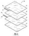
- FIG. 1is a top view of a prior art resistive touch screen
- FIG. 2is an exploded view showing layers of a prior art resistive touch screen
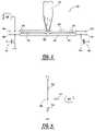
- FIG. 3is a cross-sectional view of a portion of conductive layers of a resistive touch screen being coupled together by a stylus;
- FIG. 4is a schematic diagram representative of the resistive touch screen of FIG. 3 .
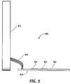
- FIG. 5is an illustration of a resistive touch screen coupled to a printed circuit board in accordance with the present invention.
- FIG. 6is a schematic diagram illustrating a resistive touch screen being touched in accordance with the present invention.
- FIG. 7is a schematic diagram illustrating circuitry for interfacing with a resistive touch screen in accordance with the present invention.
- FIG. 8is a block diagram illustrating an apparatus for inputting data in accordance with the present invention.
- FIG. 1is a top view of a prior art resistive touch screen 10 .
- Resistive touch screen 10comprises a transparent screen 11 that allows an underlying display (not shown) of an electronic system to be viewed.
- Wires 12 , 13 , 14 , and 15couple to resistive touch screen 10 .
- Wires 12 and 13couple to a first transparent conductive layer of resistive touch screen 10 .
- Wires 14 and 15couple to a second transparent conductive layer of resistive touch screen 10 .
- the first and second transparent conductive layersare not in contact with each other under quiescent conditions.
- resistive touch screen 10is shown having four wires there are many alternate embodiments having more than four wires for different screen configurations or to provide further features. In general, the various different resistive touch screens available to the consumer all operate on the same principal of creating contact between the first and second conductive layers when touched.
- FIG. 2is an exploded view showing layers of a prior art resistive touch screen 20 .
- Resistive touch screen 20comprises a protective layer 21 , a conductive layer 22 , a conductive layer 23 , and a protective hard backing layer 24 . Spacers (not shown) are placed between conductive layers 22 and 23 to prevent contact with one another under quiescent conditions.
- Protective layer 21is an outer layer of resistive touch screen 20 that is transparent, durable under contact, and scratch resistant. Protective layer 21 is exposed to the external environment and is contacted by a finger or other element such as a stylus or pen.
- Conductive layers 22 and 23are manufactured from a conductive transparent material. Typically, conductive layers 22 and 23 comprise indium tin oxide (ITO) or a resistive polyester material. The ITO can be deposited on a substrate such as glass if desired. In general, the resistance of conductive layers 22 and 23 fall within a range of 100 to 900 ohms. Spacing between conductive layers 22 and 23 is maintained by uniformly distributed spacer dots. Wires 25 and 26 couple to conductive layer 22 . Wires 27 and 28 couple to conductive layer 23 . One wire pair is coupled in the x-direction while the other wire pair is coupled in the y-direction.
- ITOindium tin oxide
- the ITOcan be deposited on a substrate such as glass if desired.
- the resistance of conductive layers 22 and 23fall within a range of 100 to 900 ohms. Spacing between conductive layers 22 and 23 is maintained by uniformly distributed spacer dots.
- Wires 25 and 26couple to conductive
- conductive layer 22is coupled such that wires 25 and 26 are respectively coupled in the y-direction on opposing sides of the resistive material.
- conductive layer 23is coupled such that wires 27 and 28 are respectively coupled in the x-direction on opposing sides of the resistive material. This allows conductive layers 22 and 23 to conduct a current by coupling the resistive layer between a reference voltage and ground.
- Hard backing layer 24is a transparent support structure to provide rigidity and strength to resistive touch screen 20 .
- Protective layer 21 and conductive layers 22 and 23overlie hard backing layer 24 .
- FIG. 3is a cross-sectional view of a portion of conductive layers of a resistive touch screen 30 being coupled together by a stylus 33 .
- a conductive layer 31 and a conductive layer 32are shown of the resistive touch screen. Under quiescent conditions, conductive layers 31 and 32 are separated from one another by spacer dots 34 .
- Stylus 33couples to conductive layer 31 deforming a surface of conductive layer 31 to contact conductive layer 32 at an area 39 .
- conductive layer 31is coupled to an electrode 35 and an electrode 36 . Electrodes 35 and 36 are coupled to opposing ends of conductive layer 31 in the y-direction.
- Conductive layer 32is coupled to an electrode 37 and an electrode 38 . Electrodes 37 and 38 are coupled to opposing ends of conductive layer 32 in the x-direction.
- conductive layers 31 and 32are coupled such that one conducts current in the x-direction while the other is coupled to conduct in the y-direction to allow a location on a screen to be identified when touched.
- the illustrationshows one half of a prior art methodology for determining a location of area 39 where contact is made on resistive touch screen 30 .
- the location in the x-directionis determined.
- Transistor 40couples a voltage V ref to electrode 37 when enabled.
- Transistor 41couples electrode 38 to ground when enabled.
- Transistors 40 and 41are enabled simultaneously to detect the x-direction position of area 39 . Enabling transistors 40 and 41 biases conductive layer 32 to conduct a current. The resistance of conductive layer 32 is uniformly distributed from electrode 37 to electrode 38 .
- the location in the x-directionis determined by sensing a voltage at area 39 .
- FIG. 4is a schematic diagram representative of resistive touch screen 30 of FIG. 3 .
- Area 39corresponds to a location where conductive layers 31 and 32 contact one another and defines a resistor 51 and a resistor 52 in conductive layer 32 .
- Resistor 51is the resistance of conductive layer 32 from electrode 37 to area 39 .
- Resistor 52is the resistance of conductive layer 32 from area 39 to electrode 38 .
- Resistors 51 and 52form a resistor divider where the voltage at area 39 corresponds to the location in the x-direction where stylus 33 of FIG. 3 contacts the resistive touch screen.
- the voltage at area 39is sensed through conductive layer 31 and coupled to electrode 36 .
- Resistor 53is the resistance of conductive layer 31 from area 39 to electrode 36 .
- Electrode 36couples to an analog to digital converter (DAC) 42 that converts the voltage at area 39 to a corresponding digital word. Resistor 53 and DAC 42 will have little impact on the measured voltage if the input resistance of DAC 42 is high in relation to the resistance value of resistors 51 , 52 , and 53 .
- DACanalog to digital converter
- sensing the location of the location of area 39 in the y-directionis achieved by applying the same methodology to conductive layer 31 .
- a reference and ground voltageis respectively coupled to electrodes 35 and 36 of conductive layer 31 .
- a digital to analog converteris coupled to electrode 38 of conductive layer 32 .
- a resistor divideris now formed in the y-direction through conductive layer 31 and the voltage at area 39 is detected through conductive layer 32 .
- the voltage at area 39corresponds to the location of area 39 in the y-direction. Note that both the x-direction and the y-direction are calculated to locate the position on the resistive touch screen where stylus 33 causes conductive layer 31 to contact conductive layer 32 in area 39 .
- the resistive touch screen in a quiescent conditionis continuously switching back and forth between biasing conducting layers 31 and 32 .
- the voltage sensed by the analog to digital converter coupled to either conductive layers 31 and 32 under quiescent conditionsdoes not change substantially. Touching the resistive screen produces a change in voltage to the analog to digital converter indicating information is being input.
- the methodology described hereinabove for detecting a point of contact on a resistive touch screenhas several issues.
- First, switching between biasing conductive layers 31 and 32creates a significant amount of noise and voltage spikes. The noise can produce erroneous results or reduce the accuracy of measurements when coupled to the interface circuitry of the resistive touch screen.
- Second, switching between biasing conductive layers 31 and 32is very power inefficient since power is dissipated whether the resistive touch screen is being used or not.
- the wires from the resistive touch screenare often accessible as they couple to a main circuit board. Security can be compromised by someone coupling to the wires to detect the voltage changes that occur when the resistive touch screen is touched. Monitoring the voltage changes is easily converted to the data being input thus allowing someone to obtain information such as a password or signature to access an account and illegally obtain the contents of the account.
- FIG. 5is an illustration of a resistive touch screen 61 coupled to a printed circuit board 63 in accordance with the present invention.
- resistive touch screen 61is coupled by wires 62 to printed circuit board 63 that are exposed and accessible for tapping or monitoring making them a security threat for sensitive information.
- Integrated circuits 64are coupled together by interconnect on printed circuit board 63 to form an interface circuit for processing signals on wires 62 from resistive touch screen 61 .
- resistive touch screen 61is biased such that the voltage on wires 62 remain constant during quiescent conditions or when data is being input (screen 61 is touched). The data being input is more secure because monitoring the voltage on wires 62 does not yield any usable information because the voltage on each wire does not change.
- FIG. 6is a schematic diagram illustrating a resistive touch screen 70 being touched in accordance with the present invention.
- the schematic representationis simplified to show the operation of resistive touch screen 70 .
- resistive touch screenhas a first conductive layer and a second conductive layer that under quiescent conditions do not contact one another.
- One conductive layeris biased such that current flows in the y-direction and the other such that current flows in the x-direction.
- the first conductive layerhas a first electrode and a second electrode coupled to opposing ends of the first conductive layer in the y-direction.
- the first and second electrode of the first conductive layerare coupled to the same reference voltage V refY .
- the second conductive layerhas a first electrode and a second electrode coupled to opposing ends of the second conductive layer in the x-direction.
- the first and second electrode of the second conductive layerare coupled to a reference voltage V refX .
- Touching resistive touch screen 70causes the first and the second conductive layers to contact one another and is represented in the simplified schematic diagram in FIG. 6 .
- the first conductive layer of resistive touch screen 70is modeled as a resistor 71 and a resistor 72 .
- the second conductive layer of resistive touch screen 70is modeled as a resistor 73 and a resistor 74 .
- a resistor 75is a junction resistance at the point of contact, or the touch point where the first and second conductive layers of resistive touch screen 70 contact one another.
- currentis conducted at the first and second electrodes of the first and second conductive layers when resistive touch screen 70 is touched.
- a current I y1is conducted at the first electrode of the first conductive layer and a current I y2 is conducted at the second electrode of the first conductive layer.
- a current I x1is conducted at the first electrode of the second conductive layer and a current I x2 is conducted at the second electrode of the second conductive layer when resistive touch screen 70 is touched.
- a voltage V T1is defined as the voltage at node 76 .
- a voltage V T2is defined as the voltage at node 77 .
- Resistors 71 , 72 , 73 , 74 , and 75are respectively R 71 , R 72 , R 73 , R 74 , and R 75 .
- V T1V refX ⁇ I x1 *R 73 Equation 1
- V T1V refX ⁇ I x2 *R 74 Equation 2
- V T2V refY ⁇ I y1 *R 71 Equation 3
- V T2V refY ⁇ I y2 *R 72 Equation 4
- a resistor divider that corresponds to the relative position where contact to resistive touch screen 70 is made in the x-directionis related to the currents sensed at the first and second electrodes of the second conductive layer.
- the ratiois the position between the first and second electrodes of the second conductive layer relative to the first electrode. In other words, if the ratio is approaches 0 the touch point is close to the first electrode. Conversely, if the ratio approaches 1 the touch point is close to the second electrode.
- R 73 /( R 73 +R 74 )I x2 /( I x1 +I x2 ) Equation 8
- a resistor divider that corresponds to the relative position where contact to resistive touch screen 70 is made in the y-directionis related to the currents sensed at the first and second electrodes of the first conductive layer.
- the position of the location in the y-direction where resistive touch screen 70 is touchedcan be calculated from the currents I y1 and I y2 at the first and second electrodes of the first conductive layer of resistive touch screen 70 using equation 10.
- the ratiois the position between the first and second electrodes of the first conductive layer relative to the first electrode. In other words, if the ratio is approaches 0 the touch point is close to the first electrode. Conversely, if the ratio approaches 1 the touch point is close to the second electrode.
- R 71 /( R 71 +R 72 )I y2 /( I y1 +I y2 ) Equation 10
- the pressure on the area being touchedcan also be calculated.
- the pressurecorresponds to the value of resistor 75 .
- the pressure versus resistanceis characterized for a given resistive touch screen type because screens will differ depending on the process of manufacture. Equation 11 equates the difference in the two reference voltages (V refX and V refY ) being provided to resistive touch screen 70 to the currents and resistors.
- V refX ⁇ V refY( R 73 *I x1 ) ⁇ ( I y1 +I y2 )* R 75 ⁇ ( R 73 *I x1 ) Equation 11
- resistor R 75can then be calculated using equation 12 and correlated to the pressure for the specific screen being used.
- R 75[( R 73 *I x1 ) ⁇ ( R 73 *I x1 ) ⁇ ( V refX ⁇ V refY )]/( I y1 +I y2 ) Equation 12
- An additional benefit of sensing currents from resistive touch screen 70is that it is possible to detect when an intruder is attempting to monitor the data being input.
- the integer sum of all the currents at the first and second electrodes of the first and second conductive layers of resistive touch screen 70is zero (Kirchoff's Law).
- the current magnitudescan be examined on a periodic basis or prior to responding to data input. The current magnitudes are added together with the result being approximately zero. If the result is not zero, there would be the possibility that current is being leaked or injected by an intruder attempting to monitor data input to resistive touch screen 70 .
- An alert signalcan be output that makes the system aware of this potential problem such that appropriate actions are taken (such as shutting down the system) until the issue is resolved.
- FIG. 7is a schematic diagram illustrating circuitry for interfacing with a resistive touch screen in accordance with the present invention.
- the interface circuitrycomprises current to voltage converters 81 , 82 , 83 , and 84 , and an analog to digital converter (A/D) 85 .
- current to voltage converters 81 - 84form a detection circuit that senses currents from the resistive touch screen when touched while providing and maintaining a constant voltage to the conductive layers of the resistive touch screen.
- Each current to voltage converters 81 - 84is responsive to a current from the resistive touch screen and outputs a voltage that corresponds to the current magnitude.
- A/D converter 85converts an analog voltage coupled from current to voltage converters 81 - 84 to a corresponding digital word.
- a terminal 86 and a terminal 88respectively couples to the first and second electrodes of a first conductive layer of the resistive touch screen similar to that described in FIG. 6 .
- a terminal 87 and a terminal 89respectively couples to the first and second electrodes of a second conductive layer of the resistive touch similar to that described in FIG. 6 .
- Current to voltage converter 81comprises an amplifier 101 and a resistor 102 .
- Amplifier 101has a positive input coupled to a reference voltage V refY , a negative input coupled to terminal 86 , and an output.
- Resistor 102has a first terminal coupled to the output of amplifier 101 and a second terminal coupled to terminal 86 .
- Current to voltage converter 83comprises an amplifier 105 and a resistor 106 .
- Amplifier 105has a positive input coupled to a reference voltage V refY , a negative input coupled to terminal 88 , and an output.
- Resistor 106has a first terminal coupled to the output of amplifier 105 and a second terminal coupled to terminal 88 .
- Current to voltage converter 82comprises an amplifier 103 and a resistor 104 .
- Amplifier 103has a positive input coupled to a reference voltage V refX , a negative input coupled to terminal 87 , and an output.
- Resistor 104has a first terminal coupled to the output of amplifier 103 and a second terminal coupled to terminal 87 .
- Current to voltage converter 84comprises an amplifier 107 and a resistor 108 .
- Amplifier 107has a positive input coupled to a reference voltage V refX , a negative input coupled to terminal 89 , and an output.
- Resistor 108has a first terminal coupled to the output of amplifier 107 and a second terminal coupled to terminal 89 .
- Analog to digital converter 85has an input channel 91 coupled to the output of amplifier 101 , an input channel 92 coupled to the output of amplifier 103 , an input channel 93 coupled to the output of amplifier 105 , an input channel 94 coupled to the output of amplifier 107 , and a digital output bus 111 .
- the detection circuitprovides the constant reference voltages (V refX and V refY ) to the resistive touch screen.
- current to voltage converters 81 - 84operate similarly, each being coupled to a reference voltage (either V refX and V refY ).
- amplifiers 101 , 103 , 105 , and 107are configured to drive the output to a voltage that forces the negative input of the amplifier to be an equal voltage as the positive input. In other words, the amplifier will always drive the negative input to a voltage substantially equal to the reference voltage (V refX or V refY ) coupled to the positive input of the amplifier.
- terminals 86 and 88output a voltage of approximately V refY and terminals 87 and 89 output a voltage of approximately V refX .
- terminals 86 - 89couple to the resistive touch screen.
- the voltage at terminals 86 - 89remain substantially constant under both quiescent conditions and when the resistive touch screen is touched thereby enhancing security by preventing information from being stolen by sensing voltage changes on the lines coupling the resistive touch screen to the interface circuitry.
- the positive input of amplifier 101is coupled to a voltage V refY .
- Amplifier 101drives the output to a voltage that yields a voltage of approximately V refY at the negative input of amplifier 101 .
- the output of amplifier 101couples through resistor 102 to terminal 86 .
- the resistive touch screenoutputs substantially zero current as described in FIG. 6 .
- the output of amplifier 101 under quiescent conditionsis at a voltage of approximately V refY .
- a current received at terminal 86changes the voltage across resistor 102 thereby changing the voltage at the negative input of amplifier 101 .
- Amplifier 101responds immediately to the differential voltage created across the positive and negative inputs of amplifier 101 generating a voltage at the output of amplifier 101 that reduces the differential voltage to approximately zero volts.
- Amplifier 101responds to any current change at terminal 86 to maintain the voltage at V refY .
- the voltage at the output of amplifier 101 that maintains the voltage at V refYcorresponds to the current at terminal 86 .
- the currentis calculated from the known voltages at either terminal of resistor 102 and the resistance value of resistor 102 .
- Current to voltage converters 82 , 83 , and 84respond similar to changes in current respectively at terminals 87 , 88 , and 89 .
- Analog to digital converter 85receives the voltages at the outputs of amplifiers 101 , 103 , 105 , and 107 respectively at input channels 91 - 94 .
- each input channel of A/D converter 85can be selected to sample and convert the voltage to a corresponding digital word.
- A/D converter 85samples and outputs a digital word for each amplifier of the detection circuit sequentially.
- Digital output bus 111couples to a microcontroller, microprocessor, digital signal processing unit, or other logic unit that is capable of receiving the digital words output by A/D converter 85 (corresponding to currents at each electrode of the resistive touch screen) and computing the location where the screen was touched using the model described in FIG. 6 .
- the pressurecan also be calculated from the currents output from the resistive touch screen.
- the resistive touch screendissipates little or no power under quiescent conditions.
- the electrodes of a conductive layerare coupled to equal voltages producing a net differential voltage of zero across the conductive layer.
- Further power savingsare achieved in the exemplary embodiment by lowering the reference voltage applied to each conductive layer of the resistive touch screen.
- the voltagecan be lowered because a current, not voltage, is being detected from the resistive touch screen.
- Prior art resistive touch screen interface circuitsoperate at substantially higher voltages (e.g., five volts).
- the scan ratecan be increased to the level of the analog to digital converter, thereby increasing the performance of the system. This results in an increase in sensing accuracy and a reduction in the time required to determine the location where the resistive touch screen is being touched.
- FIG. 8is a block diagram illustrating an apparatus for inputting data in accordance with the present invention.
- a detection circuit 123is responsive to a resistive touch screen 120 .
- resistive touch screen 120is coupled to detection circuit 123 through wires 131 - 134 .
- Resistive touch screen 120includes a first conductive layer and a second conductive layer. Wires 131 and 132 couple to a first and a second electrode of the first conductive layer. Wires 133 and 134 couple to a first and a second electrode of the second conductive layer.
- the first and second electrodes of the first conductive layer of resistive touch screen 120couple to opposing ends of the first conductive layer. Similarly, the first and second electrodes of the second conductive layer of resistive touch screen 120 couple to opposing ends of the second conductive layer.
- the direction of current flow Through the first and second conductive layersare chosen to have different orientations thereby allowing a location where the first and second conductive layers contact one another to be determined when resistive touch screen is touched.
- the first and second electrodes of the first conductive layerare oriented so that current flows through the first conductive layer in the y-direction.
- the first and second electrodes of the second conductive layerare oriented so current flows through the second conductive layer in the x-direction. It should be noted that other orientations could be used and that the different orientations could be applied to either conductive layer of the resistive touch screen.
- Detection circuit 123provides a first reference voltage to wires 131 and 132 thus applying equal voltage to the first and second electrode of the first conductive layer of resistive touch screen 120 .
- a second reference voltageis provided to wires 133 and 134 by detection circuit 123 thus applying equal voltage to the first and second electrode of the second conductive layer of resistive touch screen 120 .
- Detection circuit 123maintains the first reference voltage constant to the first conductive layer and the second reference voltage constant to the second conductive layer under quiescent conditions or when resistive touch screen 120 is touched (causing the first and second conductive layers to couple to one another).
- the voltage on wires 131 - 134remain substantially constant during operation of resistive touch screen 120 .
- detection circuit 123comprises four current to voltage converters.
- Wires 131 - 134couple currents to detection circuit 123 when resistive touch screen 120 is touched causing the first conductive layer to couple to the second conductive layer.
- the magnitude of the currents on each wirecorrespond to a location where resistive touch screen 120 is touched as described in detail in FIG. 6 .
- Detection circuit 123maintains constant voltages on wires 131 - 134 and outputs voltages corresponding to the magnitude of the currents received.
- detection circuit 123an analog to digital (A/D) converter 124 , and a microcontroller 125 are coupled to a substrate 122 .
- substrate 122is a printed circuit board having interconnect to couple detection circuit 123 , A/D converter 124 , and microcontroller 123 together.
- A/D converter 124is responsive to detection circuit 123 .
- A/D converter 124converts voltages output by detection circuit 123 to digital words corresponding to the voltage levels.
- the digital wordsare provided to microcontroller 125 .
- Microcontroller 125calculates a location of where resistive touch screen 120 is touched from the digital words. The digital words correspond to the currents produced by resistive touch screen 120 when touched.
- microcontroller 125calculates the location using equations derived and described in FIG. 6 .
- Microcontroller 125can also calculate the pressure applied to resistive touch screen 120 when touched as described in FIG. 6 .
Landscapes
- Engineering & Computer Science (AREA)
- General Engineering & Computer Science (AREA)
- Theoretical Computer Science (AREA)
- Human Computer Interaction (AREA)
- Physics & Mathematics (AREA)
- General Physics & Mathematics (AREA)
- Position Input By Displaying (AREA)
Abstract
Description
VT1=VrefX−Ix1*R73 Equation 1
VT1=VrefX−Ix2*R74 Equation 2
VT2=VrefY−Iy1*R71 Equation 3
VT2=VrefY−Iy2*R72 Equation 4
Ix1*R73=Ix2*R74 Equation 5
Iy1*R71=Iy2*R72 Equation 6
Ix2*(R73+R74)=R73*(Ix1+Ix2) Equation 7
R73/(R73+R74)=Ix2/(Ix1+Ix2) Equation 8
Iy2*(R71+R72)=R71*(Iy1+Iy2) Equation 9
R71/(R71+R72)=Iy2/(Iy1+Iy2)
VrefX−VrefY=(R73*Ix1)−(Iy1+Iy2)*R75−(R73*Ix1)
R75=[(R73*Ix1)−(R73*Ix1)−(VrefX−VrefY)]/(Iy1+Iy2)
Claims (5)
Priority Applications (6)
| Application Number | Priority Date | Filing Date | Title |
|---|---|---|---|
| US10/750,176US7250940B2 (en) | 2003-12-31 | 2003-12-31 | Touch screen apparatus and method therefore |
| EP05704931AEP1700198A2 (en) | 2003-12-31 | 2005-01-03 | Touch screen apparatus and method therefore |
| PCT/US2005/000097WO2005066757A2 (en) | 2003-12-31 | 2005-01-03 | Touch screen apparatus and method therefore |
| JP2006547618AJP4881745B2 (en) | 2003-12-31 | 2005-01-03 | Touch screen device and method thereof |
| CN200580001863XACN1906641B (en) | 2003-12-31 | 2005-01-03 | Touch screen device and method thereof |
| JP2011021170AJP2011129148A (en) | 2003-12-31 | 2011-02-02 | Touch screen apparatus and method therefor |
Applications Claiming Priority (1)
| Application Number | Priority Date | Filing Date | Title |
|---|---|---|---|
| US10/750,176US7250940B2 (en) | 2003-12-31 | 2003-12-31 | Touch screen apparatus and method therefore |
Publications (2)
| Publication Number | Publication Date |
|---|---|
| US20050140662A1 US20050140662A1 (en) | 2005-06-30 |
| US7250940B2true US7250940B2 (en) | 2007-07-31 |
Family
ID=34701168
Family Applications (1)
| Application Number | Title | Priority Date | Filing Date |
|---|---|---|---|
| US10/750,176Expired - LifetimeUS7250940B2 (en) | 2003-12-31 | 2003-12-31 | Touch screen apparatus and method therefore |
Country Status (5)
| Country | Link |
|---|---|
| US (1) | US7250940B2 (en) |
| EP (1) | EP1700198A2 (en) |
| JP (2) | JP4881745B2 (en) |
| CN (1) | CN1906641B (en) |
| WO (1) | WO2005066757A2 (en) |
Cited By (27)
| Publication number | Priority date | Publication date | Assignee | Title |
|---|---|---|---|---|
| US20060017704A1 (en)* | 2004-07-22 | 2006-01-26 | Digitech Systems Co., Ltd. | Device for controlling touch panel |
| US20060091991A1 (en)* | 2004-10-15 | 2006-05-04 | Markus Wohlgenannt | Magneto resistive elements and methods for manufacture and use of same |
| US20080309627A1 (en)* | 2007-06-13 | 2008-12-18 | Apple Inc. | Integrated in-plane switching |
| WO2009137155A1 (en)* | 2008-05-09 | 2009-11-12 | Synaptics Incorporated | Gradient sensors |
| US20100207895A1 (en)* | 2009-02-16 | 2010-08-19 | Samsung Electro-Mechanics Co., Ltd. | Tactile interface device and method for controlling the same |
| US20110007010A1 (en)* | 2009-07-10 | 2011-01-13 | Chimei Innolux Corporation | Method for detecting a touched position on a touch device |
| US20110148668A1 (en)* | 2009-12-17 | 2011-06-23 | Shenzhen Futaihong Precision Industry Co., Ltd. | System and method for protecting a resistive touch panel of a communication device |
| US20110254803A1 (en)* | 2010-04-20 | 2011-10-20 | Chae Kyoung Soo | Method for recognizing multi-touch of resistive touch screen |
| US8587422B2 (en) | 2010-03-31 | 2013-11-19 | Tk Holdings, Inc. | Occupant sensing system |
| US8725230B2 (en) | 2010-04-02 | 2014-05-13 | Tk Holdings Inc. | Steering wheel with hand sensors |
| US8837670B2 (en) | 2006-05-05 | 2014-09-16 | Rapiscan Systems, Inc. | Cargo inspection system |
| US8908831B2 (en) | 2011-02-08 | 2014-12-09 | Rapiscan Systems, Inc. | Covert surveillance using multi-modality sensing |
| US20140368758A1 (en)* | 2013-06-17 | 2014-12-18 | Boe Technology Group Co., Ltd. | Optical touch screen and method for manufacturing the same |
| TWI469029B (en)* | 2009-07-15 | 2015-01-11 | Chimei Innolux Corp | Method for detecting a touched position on a touch device |
| US8954848B2 (en) | 2009-12-18 | 2015-02-10 | Honda Motor Co., Ltd. | Morphable pad for tactile control |
| US9007190B2 (en) | 2010-03-31 | 2015-04-14 | Tk Holdings Inc. | Steering wheel sensors |
| US9052403B2 (en) | 2002-07-23 | 2015-06-09 | Rapiscan Systems, Inc. | Compact mobile cargo scanning system |
| US9218933B2 (en) | 2011-06-09 | 2015-12-22 | Rapidscan Systems, Inc. | Low-dose radiographic imaging system |
| US9223049B2 (en) | 2002-07-23 | 2015-12-29 | Rapiscan Systems, Inc. | Cargo scanning system with boom structure |
| US9223050B2 (en) | 2005-04-15 | 2015-12-29 | Rapiscan Systems, Inc. | X-ray imaging system having improved mobility |
| US9285498B2 (en) | 2003-06-20 | 2016-03-15 | Rapiscan Systems, Inc. | Relocatable X-ray imaging system and method for inspecting commercial vehicles and cargo containers |
| US9332624B2 (en) | 2008-05-20 | 2016-05-03 | Rapiscan Systems, Inc. | Gantry scanner systems |
| US9557427B2 (en) | 2014-01-08 | 2017-01-31 | Rapiscan Systems, Inc. | Thin gap chamber neutron detectors |
| US9625606B2 (en) | 2009-05-16 | 2017-04-18 | Rapiscan Systems, Inc. | Systems and methods for high-Z threat alarm resolution |
| US9696223B2 (en) | 2012-09-17 | 2017-07-04 | Tk Holdings Inc. | Single layer force sensor |
| US9727031B2 (en) | 2012-04-13 | 2017-08-08 | Tk Holdings Inc. | Pressure sensor including a pressure sensitive material for use with control systems and methods of using the same |
| US9791590B2 (en) | 2013-01-31 | 2017-10-17 | Rapiscan Systems, Inc. | Portable security inspection system |
Families Citing this family (19)
| Publication number | Priority date | Publication date | Assignee | Title |
|---|---|---|---|---|
| US20070247444A1 (en)* | 2006-04-20 | 2007-10-25 | Egalax Inc. | Method for measuring pressure resistance of touch panel |
| US7929287B2 (en)* | 2007-07-05 | 2011-04-19 | Sony Corporation | Electronic apparatus |
| US8619040B2 (en)* | 2007-07-05 | 2013-12-31 | Sony Corporation | Electronic apparatus |
| US7868877B2 (en)* | 2007-10-18 | 2011-01-11 | Freescale Semiconductor, Inc. | Touch panel detection circuitry and method of operation |
| TWI365394B (en)* | 2008-09-11 | 2012-06-01 | First Int Computer Inc | Operating apparatus for hand-held electronic apparatus and method thereof |
| KR101511162B1 (en)* | 2008-12-01 | 2015-04-13 | 삼성전자주식회사 | Multi touch sensing circuit |
| US20100164905A1 (en)* | 2008-12-29 | 2010-07-01 | Stmicroelectronics Asia Pacific Pte, Ltd. | Method of improved computation of touch coordinates for four-wire resistive touch screens |
| KR101613327B1 (en)* | 2009-02-27 | 2016-04-18 | 가부시키가이샤 재팬 디스프레이 | Display device, touch panel, and electronic equipment |
| US20110012760A1 (en)* | 2009-07-14 | 2011-01-20 | Sony Ericsson Mobile Communications Ab | Touch sensing device, touch screen device including a touch sensing device, mobile device and method for sensing a touch on a touch sensing device |
| CN101996016B (en)* | 2009-08-26 | 2013-01-02 | 深圳华映显示科技有限公司 | Method for sensing touch event and digital resistance type touch panel |
| CN101866254A (en)* | 2010-04-09 | 2010-10-20 | 鸿富锦精密工业(深圳)有限公司 | Resistive touch screen and display device thereof |
| US8537128B2 (en)* | 2010-06-21 | 2013-09-17 | Apple Inc. | Portable multi-touch input device |
| TWI470677B (en)* | 2011-02-25 | 2015-01-21 | Hannstar Display Corp | Method for fabricating touch panel |
| KR101891475B1 (en) | 2012-01-06 | 2018-09-28 | 삼성전자 주식회사 | Display apparatus and control method thereof, input apparatus, display system |
| CN103258171B (en)* | 2012-02-20 | 2016-03-02 | 中国移动通信集团公司 | Prevent the method for mobile terminal touch screen error touch control, device and mobile terminal |
| CN103345338B (en)* | 2013-06-17 | 2016-12-28 | 合肥京东方光电科技有限公司 | Light touch screen and preparation method thereof |
| JP2015011584A (en)* | 2013-06-28 | 2015-01-19 | 株式会社翔栄 | Vending machine touch panel |
| CN103950333A (en)* | 2014-04-18 | 2014-07-30 | 大连民族学院 | Novel intelligent pen container |
| CN106771756A (en)* | 2016-12-28 | 2017-05-31 | 京东方科技集团股份有限公司 | Brush roll is pressed into quantity sensor and measurement apparatus |
Citations (14)
| Publication number | Priority date | Publication date | Assignee | Title |
|---|---|---|---|---|
| US4623757A (en) | 1984-11-29 | 1986-11-18 | Interaction Systems, Inc. | Method and apparatus for electronic touch mapping |
| JPH06348390A (en) | 1993-06-01 | 1994-12-22 | Nitsuko Corp | Input coordinate detecting device |
| US5859392A (en)* | 1996-02-09 | 1999-01-12 | Lsi Logic Corporation | Method and apparatus for reducing noise in an electrostatic digitizing tablet |
| US6061051A (en) | 1997-01-17 | 2000-05-09 | Tritech Microelectronics | Command set for touchpad pen-input mouse |
| US6075520A (en)* | 1996-11-15 | 2000-06-13 | Rohm Co., Ltd. | Small current detector circuit and locator device using the same |
| US6278444B1 (en) | 1998-08-21 | 2001-08-21 | Geoffrey D. Wilson | Low current four-wire interface for five-wire resistive touch-screen |
| US6411284B1 (en)* | 1999-09-08 | 2002-06-25 | Ncr Corporation | Methods and apparatus for providing secure signals from a touch panel display |
| US20020101407A1 (en) | 2001-01-31 | 2002-08-01 | Mobigence, Inc. | Touch panel coordinate determination |
| US6483498B1 (en)* | 1999-03-17 | 2002-11-19 | International Business Machines Corporation | Liquid crystal display with integrated resistive touch sensor |
| US6501529B1 (en) | 1999-08-18 | 2002-12-31 | International Business Machines Corporation | Liquid crystal display element integrated with a touch sensor |
| US6630896B1 (en) | 2000-05-16 | 2003-10-07 | Ncr Corporation | System and method for preventing detection of touch screen input data |
| US20030222857A1 (en)* | 2002-03-01 | 2003-12-04 | Adiel Abileah | Reflection resistant touch screens |
| US6975307B2 (en)* | 2001-10-12 | 2005-12-13 | High Tech Computer, Corp. | Method for detecting touch-point coordinate for use in a resistive touch panel |
| US6980201B1 (en)* | 2000-09-29 | 2005-12-27 | Rockwell Automation Technologies, Inc. | Minimum move touch plane scanning method and device |
Family Cites Families (1)
| Publication number | Priority date | Publication date | Assignee | Title |
|---|---|---|---|---|
| JP2002278690A (en)* | 2001-03-19 | 2002-09-27 | Aiphone Co Ltd | Position detecting circuit for touch panel |
- 2003
- 2003-12-31USUS10/750,176patent/US7250940B2/ennot_activeExpired - Lifetime
- 2005
- 2005-01-03JPJP2006547618Apatent/JP4881745B2/ennot_activeExpired - Lifetime
- 2005-01-03CNCN200580001863XApatent/CN1906641B/ennot_activeExpired - Lifetime
- 2005-01-03EPEP05704931Apatent/EP1700198A2/ennot_activeWithdrawn
- 2005-01-03WOPCT/US2005/000097patent/WO2005066757A2/ennot_activeApplication Discontinuation
- 2011
- 2011-02-02JPJP2011021170Apatent/JP2011129148A/enactivePending
Patent Citations (14)
| Publication number | Priority date | Publication date | Assignee | Title |
|---|---|---|---|---|
| US4623757A (en) | 1984-11-29 | 1986-11-18 | Interaction Systems, Inc. | Method and apparatus for electronic touch mapping |
| JPH06348390A (en) | 1993-06-01 | 1994-12-22 | Nitsuko Corp | Input coordinate detecting device |
| US5859392A (en)* | 1996-02-09 | 1999-01-12 | Lsi Logic Corporation | Method and apparatus for reducing noise in an electrostatic digitizing tablet |
| US6075520A (en)* | 1996-11-15 | 2000-06-13 | Rohm Co., Ltd. | Small current detector circuit and locator device using the same |
| US6061051A (en) | 1997-01-17 | 2000-05-09 | Tritech Microelectronics | Command set for touchpad pen-input mouse |
| US6278444B1 (en) | 1998-08-21 | 2001-08-21 | Geoffrey D. Wilson | Low current four-wire interface for five-wire resistive touch-screen |
| US6483498B1 (en)* | 1999-03-17 | 2002-11-19 | International Business Machines Corporation | Liquid crystal display with integrated resistive touch sensor |
| US6501529B1 (en) | 1999-08-18 | 2002-12-31 | International Business Machines Corporation | Liquid crystal display element integrated with a touch sensor |
| US6411284B1 (en)* | 1999-09-08 | 2002-06-25 | Ncr Corporation | Methods and apparatus for providing secure signals from a touch panel display |
| US6630896B1 (en) | 2000-05-16 | 2003-10-07 | Ncr Corporation | System and method for preventing detection of touch screen input data |
| US6980201B1 (en)* | 2000-09-29 | 2005-12-27 | Rockwell Automation Technologies, Inc. | Minimum move touch plane scanning method and device |
| US20020101407A1 (en) | 2001-01-31 | 2002-08-01 | Mobigence, Inc. | Touch panel coordinate determination |
| US6975307B2 (en)* | 2001-10-12 | 2005-12-13 | High Tech Computer, Corp. | Method for detecting touch-point coordinate for use in a resistive touch panel |
| US20030222857A1 (en)* | 2002-03-01 | 2003-12-04 | Adiel Abileah | Reflection resistant touch screens |
Non-Patent Citations (2)
| Title |
|---|
| Horowitz P., Hill W.: The Art of Electronics, Second Edition, 2001, Cambridge University Press, Cambridge, UK XP002339423, p. 184. |
| Wolfe A., A case study in low-power system-level design, Oct. 2, 1995, Computer Design: VLSI in computers and processors 1995. ICCD 95. Proceedings, 1995 IEEE International Conference on Austin, TX, USA, XP010197331, p. 332-338. |
Cited By (46)
| Publication number | Priority date | Publication date | Assignee | Title |
|---|---|---|---|---|
| US10007019B2 (en) | 2002-07-23 | 2018-06-26 | Rapiscan Systems, Inc. | Compact mobile cargo scanning system |
| US9223049B2 (en) | 2002-07-23 | 2015-12-29 | Rapiscan Systems, Inc. | Cargo scanning system with boom structure |
| US9052403B2 (en) | 2002-07-23 | 2015-06-09 | Rapiscan Systems, Inc. | Compact mobile cargo scanning system |
| US10670769B2 (en) | 2002-07-23 | 2020-06-02 | Rapiscan Systems, Inc. | Compact mobile cargo scanning system |
| US9285498B2 (en) | 2003-06-20 | 2016-03-15 | Rapiscan Systems, Inc. | Relocatable X-ray imaging system and method for inspecting commercial vehicles and cargo containers |
| US7479951B2 (en)* | 2004-07-22 | 2009-01-20 | Digitech Systems Co., Ltd | Device for controlling touch panel |
| US20060017704A1 (en)* | 2004-07-22 | 2006-01-26 | Digitech Systems Co., Ltd. | Device for controlling touch panel |
| US20060091991A1 (en)* | 2004-10-15 | 2006-05-04 | Markus Wohlgenannt | Magneto resistive elements and methods for manufacture and use of same |
| US8077152B2 (en)* | 2004-10-15 | 2011-12-13 | University Of Iowa Research Foundation | Magneto resistive elements and methods for manufacture and use of same |
| US9223050B2 (en) | 2005-04-15 | 2015-12-29 | Rapiscan Systems, Inc. | X-ray imaging system having improved mobility |
| US9279901B2 (en) | 2006-05-05 | 2016-03-08 | Rapiscan Systems, Inc. | Cargo inspection system |
| US8837670B2 (en) | 2006-05-05 | 2014-09-16 | Rapiscan Systems, Inc. | Cargo inspection system |
| US9348475B2 (en) | 2007-06-13 | 2016-05-24 | Apple Inc. | Integrated in-plane switching |
| US9104258B2 (en) | 2007-06-13 | 2015-08-11 | Apple Inc. | Integrated in-plane switching |
| US8274492B2 (en) | 2007-06-13 | 2012-09-25 | Apple Inc. | Integrated in-plane switching |
| US9727191B2 (en) | 2007-06-13 | 2017-08-08 | Apple Inc. | Integrated in-plane switching |
| US20080309627A1 (en)* | 2007-06-13 | 2008-12-18 | Apple Inc. | Integrated in-plane switching |
| US8040326B2 (en) | 2007-06-13 | 2011-10-18 | Apple Inc. | Integrated in-plane switching display and touch sensor |
| WO2009137155A1 (en)* | 2008-05-09 | 2009-11-12 | Synaptics Incorporated | Gradient sensors |
| US10098214B2 (en) | 2008-05-20 | 2018-10-09 | Rapiscan Systems, Inc. | Detector support structures for gantry scanner systems |
| US9332624B2 (en) | 2008-05-20 | 2016-05-03 | Rapiscan Systems, Inc. | Gantry scanner systems |
| US20100207895A1 (en)* | 2009-02-16 | 2010-08-19 | Samsung Electro-Mechanics Co., Ltd. | Tactile interface device and method for controlling the same |
| US9625606B2 (en) | 2009-05-16 | 2017-04-18 | Rapiscan Systems, Inc. | Systems and methods for high-Z threat alarm resolution |
| US8487906B2 (en)* | 2009-07-10 | 2013-07-16 | Chimel Innolux Corporation | Method for detecting a touched position on a touch device |
| US20110007010A1 (en)* | 2009-07-10 | 2011-01-13 | Chimei Innolux Corporation | Method for detecting a touched position on a touch device |
| TWI469029B (en)* | 2009-07-15 | 2015-01-11 | Chimei Innolux Corp | Method for detecting a touched position on a touch device |
| US8253710B2 (en)* | 2009-12-17 | 2012-08-28 | Shenzhen Futaihong Precision Industry Co., Ltd. | System and method for protecting a resistive touch panel of a communication device |
| US20110148668A1 (en)* | 2009-12-17 | 2011-06-23 | Shenzhen Futaihong Precision Industry Co., Ltd. | System and method for protecting a resistive touch panel of a communication device |
| US9760175B2 (en) | 2009-12-18 | 2017-09-12 | Honda Motor Co., Ltd. | Morphable pad for tactile control |
| EP3171249A1 (en) | 2009-12-18 | 2017-05-24 | Honda Motor Co., Ltd. | Morphable pad for tactile control |
| US8954848B2 (en) | 2009-12-18 | 2015-02-10 | Honda Motor Co., Ltd. | Morphable pad for tactile control |
| US9007190B2 (en) | 2010-03-31 | 2015-04-14 | Tk Holdings Inc. | Steering wheel sensors |
| US8587422B2 (en) | 2010-03-31 | 2013-11-19 | Tk Holdings, Inc. | Occupant sensing system |
| US8725230B2 (en) | 2010-04-02 | 2014-05-13 | Tk Holdings Inc. | Steering wheel with hand sensors |
| US20110254803A1 (en)* | 2010-04-20 | 2011-10-20 | Chae Kyoung Soo | Method for recognizing multi-touch of resistive touch screen |
| US9562866B2 (en) | 2011-02-08 | 2017-02-07 | Rapiscan Systems, Inc. | Covert surveillance using multi-modality sensing |
| US8908831B2 (en) | 2011-02-08 | 2014-12-09 | Rapiscan Systems, Inc. | Covert surveillance using multi-modality sensing |
| US9218933B2 (en) | 2011-06-09 | 2015-12-22 | Rapidscan Systems, Inc. | Low-dose radiographic imaging system |
| US9727031B2 (en) | 2012-04-13 | 2017-08-08 | Tk Holdings Inc. | Pressure sensor including a pressure sensitive material for use with control systems and methods of using the same |
| US9696223B2 (en) | 2012-09-17 | 2017-07-04 | Tk Holdings Inc. | Single layer force sensor |
| US9791590B2 (en) | 2013-01-31 | 2017-10-17 | Rapiscan Systems, Inc. | Portable security inspection system |
| US10317566B2 (en) | 2013-01-31 | 2019-06-11 | Rapiscan Systems, Inc. | Portable security inspection system |
| US11550077B2 (en) | 2013-01-31 | 2023-01-10 | Rapiscan Systems, Inc. | Portable vehicle inspection portal with accompanying workstation |
| US9495032B2 (en)* | 2013-06-17 | 2016-11-15 | Boe Technology Group Co., Ltd. | Optical touch screen |
| US20140368758A1 (en)* | 2013-06-17 | 2014-12-18 | Boe Technology Group Co., Ltd. | Optical touch screen and method for manufacturing the same |
| US9557427B2 (en) | 2014-01-08 | 2017-01-31 | Rapiscan Systems, Inc. | Thin gap chamber neutron detectors |
Also Published As
| Publication number | Publication date |
|---|---|
| EP1700198A2 (en) | 2006-09-13 |
| US20050140662A1 (en) | 2005-06-30 |
| JP2011129148A (en) | 2011-06-30 |
| WO2005066757A3 (en) | 2005-09-29 |
| CN1906641B (en) | 2010-05-12 |
| CN1906641A (en) | 2007-01-31 |
| JP2007517342A (en) | 2007-06-28 |
| WO2005066757A2 (en) | 2005-07-21 |
| JP4881745B2 (en) | 2012-02-22 |
Similar Documents
| Publication | Publication Date | Title |
|---|---|---|
| US7250940B2 (en) | Touch screen apparatus and method therefore | |
| US20090322700A1 (en) | Method and apparatus for detecting two simultaneous touches and gestures on a resistive touchscreen | |
| US9632622B2 (en) | Ground detection for touch sensitive device | |
| EP2413224B1 (en) | Compensation for capacitance change in touch sensing device | |
| US9075483B2 (en) | Negative pixel compensation | |
| CN201638189U (en) | Equipment and system for compensating negative pixel effect on touch sensor panel | |
| US6054979A (en) | Current sensing touchpad for computers and the like | |
| CN102326138B (en) | Method and apparatus for two-finger touch coordinate recognition and rotation gesture recognition | |
| CN105677130B (en) | Pressure sensitivity touch control method, pressure sensitivity touch device and pressure-sensitive touch screen | |
| US20090237374A1 (en) | Transparent pressure sensor and method for using | |
| US20040140958A1 (en) | Method and apparatus for avoiding pressing inaccuracies on a touch panel | |
| US20100026654A1 (en) | Coordinate input device | |
| WO2010005498A2 (en) | Method and apparatus for detecting two simultaneous touches and gestures on a resistive touchscreen | |
| CN102804115A (en) | Touch- or proximity-sensitive interface | |
| TW201207710A (en) | Method and device for analyzing positions | |
| TW200917111A (en) | Resistive type multi-touch control panel and its detection method | |
| JP2010272143A (en) | Dual sensor touch screen using projected capacitive sensor and pressure sensitive touch sensor | |
| US20060066589A1 (en) | Input device | |
| CN102830870B (en) | Sensor is arranged | |
| TW201108065A (en) | Method for identifying interaction and integrated circuit device | |
| JPH1097382A (en) | Terminal device with touch screen and touch screen | |
| CN102681652B (en) | A method and terminal for realizing safe input | |
| KR20100011084A (en) | Method for securing password of a touch sensing device and apparatus thereof | |
| WO2014134265A2 (en) | Protecting physical signal paths using capacitive sensing techniques | |
| CN109343731A (en) | Touch control display and its touch control detecting method |
Legal Events
| Date | Code | Title | Description |
|---|---|---|---|
| AS | Assignment | Owner name:SYMBOL TECHNOLOGIES, INC., NEW YORK Free format text:ASSIGNMENT OF ASSIGNORS INTEREST;ASSIGNORS:JAYANETTI, RUWAN;FERNANDO, LLAVANYA;REEL/FRAME:014322/0161 Effective date:20040128 | |
| STCF | Information on status: patent grant | Free format text:PATENTED CASE | |
| AS | Assignment | Owner name:AMERICAN SCIENCE AND ENGINEERING, INC., MASSACHUSE Free format text:RELEASE;ASSIGNOR:SILICON VALLEY BANK;REEL/FRAME:023557/0032 Effective date:20091118 | |
| FPAY | Fee payment | Year of fee payment:4 | |
| AS | Assignment | Owner name:MORGAN STANLEY SENIOR FUNDING, INC. AS THE COLLATERAL AGENT, MARYLAND Free format text:SECURITY AGREEMENT;ASSIGNORS:ZIH CORP.;LASER BAND, LLC;ZEBRA ENTERPRISE SOLUTIONS CORP.;AND OTHERS;REEL/FRAME:034114/0270 Effective date:20141027 Owner name:MORGAN STANLEY SENIOR FUNDING, INC. AS THE COLLATE Free format text:SECURITY AGREEMENT;ASSIGNORS:ZIH CORP.;LASER BAND, LLC;ZEBRA ENTERPRISE SOLUTIONS CORP.;AND OTHERS;REEL/FRAME:034114/0270 Effective date:20141027 | |
| FPAY | Fee payment | Year of fee payment:8 | |
| AS | Assignment | Owner name:SYMBOL TECHNOLOGIES, LLC, NEW YORK Free format text:CHANGE OF NAME;ASSIGNOR:SYMBOL TECHNOLOGIES, INC.;REEL/FRAME:036083/0640 Effective date:20150410 | |
| AS | Assignment | Owner name:SYMBOL TECHNOLOGIES, INC., NEW YORK Free format text:RELEASE BY SECURED PARTY;ASSIGNOR:MORGAN STANLEY SENIOR FUNDING, INC.;REEL/FRAME:036371/0738 Effective date:20150721 | |
| MAFP | Maintenance fee payment | Free format text:PAYMENT OF MAINTENANCE FEE, 12TH YEAR, LARGE ENTITY (ORIGINAL EVENT CODE: M1553); ENTITY STATUS OF PATENT OWNER: LARGE ENTITY Year of fee payment:12 |