US7250626B2 - Probe testing structure - Google Patents
Probe testing structureDownload PDFInfo
- Publication number
- US7250626B2 US7250626B2US10/794,246US79424604AUS7250626B2US 7250626 B2US7250626 B2US 7250626B2US 79424604 AUS79424604 AUS 79424604AUS 7250626 B2US7250626 B2US 7250626B2
- Authority
- US
- United States
- Prior art keywords
- conductive
- substrate
- conductive member
- calibration
- probe
- Prior art date
- Legal status (The legal status is an assumption and is not a legal conclusion. Google has not performed a legal analysis and makes no representation as to the accuracy of the status listed.)
- Expired - Lifetime
Links
Images


Classifications
- G—PHYSICS
- G01—MEASURING; TESTING
- G01R—MEASURING ELECTRIC VARIABLES; MEASURING MAGNETIC VARIABLES
- G01R27/00—Arrangements for measuring resistance, reactance, impedance, or electric characteristics derived therefrom
- G01R27/02—Measuring real or complex resistance, reactance, impedance, or other two-pole characteristics derived therefrom, e.g. time constant
- G—PHYSICS
- G01—MEASURING; TESTING
- G01R—MEASURING ELECTRIC VARIABLES; MEASURING MAGNETIC VARIABLES
- G01R1/00—Details of instruments or arrangements of the types included in groups G01R5/00 - G01R13/00 and G01R31/00
- G01R1/02—General constructional details
- G01R1/06—Measuring leads; Measuring probes
- G01R1/067—Measuring probes
- G—PHYSICS
- G01—MEASURING; TESTING
- G01R—MEASURING ELECTRIC VARIABLES; MEASURING MAGNETIC VARIABLES
- G01R35/00—Testing or calibrating of apparatus covered by the other groups of this subclass
- G01R35/005—Calibrating; Standards or reference devices, e.g. voltage or resistance standards, "golden" references
- G—PHYSICS
- G01—MEASURING; TESTING
- G01R—MEASURING ELECTRIC VARIABLES; MEASURING MAGNETIC VARIABLES
- G01R27/00—Arrangements for measuring resistance, reactance, impedance, or electric characteristics derived therefrom
- G01R27/02—Measuring real or complex resistance, reactance, impedance, or other two-pole characteristics derived therefrom, e.g. time constant
- G01R27/04—Measuring real or complex resistance, reactance, impedance, or other two-pole characteristics derived therefrom, e.g. time constant in circuits having distributed constants, e.g. having very long conductors or involving high frequencies
- G—PHYSICS
- G01—MEASURING; TESTING
- G01R—MEASURING ELECTRIC VARIABLES; MEASURING MAGNETIC VARIABLES
- G01R29/00—Arrangements for measuring or indicating electric quantities not covered by groups G01R19/00 - G01R27/00
- G01R29/26—Measuring noise figure; Measuring signal-to-noise ratio
- G—PHYSICS
- G01—MEASURING; TESTING
- G01R—MEASURING ELECTRIC VARIABLES; MEASURING MAGNETIC VARIABLES
- G01R31/00—Arrangements for testing electric properties; Arrangements for locating electric faults; Arrangements for electrical testing characterised by what is being tested not provided for elsewhere
- G01R31/26—Testing of individual semiconductor devices
- G—PHYSICS
- G01—MEASURING; TESTING
- G01R—MEASURING ELECTRIC VARIABLES; MEASURING MAGNETIC VARIABLES
- G01R31/00—Arrangements for testing electric properties; Arrangements for locating electric faults; Arrangements for electrical testing characterised by what is being tested not provided for elsewhere
- G01R31/28—Testing of electronic circuits, e.g. by signal tracer
- G01R31/2851—Testing of integrated circuits [IC]
- G—PHYSICS
- G01—MEASURING; TESTING
- G01R—MEASURING ELECTRIC VARIABLES; MEASURING MAGNETIC VARIABLES
- G01R31/00—Arrangements for testing electric properties; Arrangements for locating electric faults; Arrangements for electrical testing characterised by what is being tested not provided for elsewhere
- G01R31/50—Testing of electric apparatus, lines, cables or components for short-circuits, continuity, leakage current or incorrect line connections
- G—PHYSICS
- G01—MEASURING; TESTING
- G01R—MEASURING ELECTRIC VARIABLES; MEASURING MAGNETIC VARIABLES
- G01R35/00—Testing or calibrating of apparatus covered by the other groups of this subclass
- G—PHYSICS
- G01—MEASURING; TESTING
- G01R—MEASURING ELECTRIC VARIABLES; MEASURING MAGNETIC VARIABLES
- G01R35/00—Testing or calibrating of apparatus covered by the other groups of this subclass
- G01R35/005—Calibrating; Standards or reference devices, e.g. voltage or resistance standards, "golden" references
- G01R35/007—Standards or reference devices, e.g. voltage or resistance standards, "golden references"
- H—ELECTRICITY
- H01—ELECTRIC ELEMENTS
- H01L—SEMICONDUCTOR DEVICES NOT COVERED BY CLASS H10
- H01L23/00—Details of semiconductor or other solid state devices
- H01L23/58—Structural electrical arrangements for semiconductor devices not otherwise provided for, e.g. in combination with batteries
- H—ELECTRICITY
- H01—ELECTRIC ELEMENTS
- H01P—WAVEGUIDES; RESONATORS, LINES, OR OTHER DEVICES OF THE WAVEGUIDE TYPE
- H01P1/00—Auxiliary devices
- H—ELECTRICITY
- H01—ELECTRIC ELEMENTS
- H01P—WAVEGUIDES; RESONATORS, LINES, OR OTHER DEVICES OF THE WAVEGUIDE TYPE
- H01P1/00—Auxiliary devices
- H01P1/16—Auxiliary devices for mode selection, e.g. mode suppression or mode promotion; for mode conversion
- H—ELECTRICITY
- H01—ELECTRIC ELEMENTS
- H01P—WAVEGUIDES; RESONATORS, LINES, OR OTHER DEVICES OF THE WAVEGUIDE TYPE
- H01P3/00—Waveguides; Transmission lines of the waveguide type
- H01P3/02—Waveguides; Transmission lines of the waveguide type with two longitudinal conductors
- H01P3/08—Microstrips; Strip lines
- H—ELECTRICITY
- H10—SEMICONDUCTOR DEVICES; ELECTRIC SOLID-STATE DEVICES NOT OTHERWISE PROVIDED FOR
- H10D—INORGANIC ELECTRIC SEMICONDUCTOR DEVICES
- H10D30/00—Field-effect transistors [FET]
- H10D30/80—FETs having rectifying junction gate electrodes
- H—ELECTRICITY
- H10—SEMICONDUCTOR DEVICES; ELECTRIC SOLID-STATE DEVICES NOT OTHERWISE PROVIDED FOR
- H10F—INORGANIC SEMICONDUCTOR DEVICES SENSITIVE TO INFRARED RADIATION, LIGHT, ELECTROMAGNETIC RADIATION OF SHORTER WAVELENGTH OR CORPUSCULAR RADIATION
- H10F30/00—Individual radiation-sensitive semiconductor devices in which radiation controls the flow of current through the devices, e.g. photodetectors
- H10F30/20—Individual radiation-sensitive semiconductor devices in which radiation controls the flow of current through the devices, e.g. photodetectors the devices having potential barriers, e.g. phototransistors
- H10F30/21—Individual radiation-sensitive semiconductor devices in which radiation controls the flow of current through the devices, e.g. photodetectors the devices having potential barriers, e.g. phototransistors the devices being sensitive to infrared, visible or ultraviolet radiation
- H10F30/28—Individual radiation-sensitive semiconductor devices in which radiation controls the flow of current through the devices, e.g. photodetectors the devices having potential barriers, e.g. phototransistors the devices being sensitive to infrared, visible or ultraviolet radiation the devices being characterised by field-effect operation, e.g. junction field-effect phototransistors
- G—PHYSICS
- G01—MEASURING; TESTING
- G01R—MEASURING ELECTRIC VARIABLES; MEASURING MAGNETIC VARIABLES
- G01R1/00—Details of instruments or arrangements of the types included in groups G01R5/00 - G01R13/00 and G01R31/00
- G01R1/02—General constructional details
- G01R1/06—Measuring leads; Measuring probes
- G01R1/067—Measuring probes
- G01R1/06772—High frequency probes
Definitions
- the present inventionrelates to calibration structures for probing devices, and more particularly to improved calibration structures for suppressing undesirable electromagnetic modes resulting from the substrate of the calibration structure.
- Coplanar transmission structuressuch as coplanar waveguides, coplanar striplines, coplanar slotlines, and the like, are used in a wide variety of electronic applications.
- coplanar waveguidesare used in probes suitable to probe semiconductors at multi-gigahertz frequencies, such as described in U.S. Pat. No. 4,697,143.
- the probe described in the '143 patenthas an approximately triangular shaped alumina substrate on which is formed a coplanar waveguide that tapers toward the point of the triangle.
- Bulk microwave absorbing material containing iron or ferrite and having a high magnetic loss coefficientis secured on both surfaces of the substrate to reduce the effect of unwanted propagation modes.
- One of these propagation modesincludes energy that propagates up the probe substrate and reflects off of the probe mounting block and propagates back down the substrate producing undesired distortions of the measured signals.
- Probesallow relatively accurate on-wafer measurements of very small devices, such as transistors, inductors, capacitors, resistors, and the like at frequencies from direct current to hundreds of giga-hertz. Relatively accurate measurements can be made using one or more such probes connected to a vector network analyzer and then calibrating the system using a calibration substrate.
- the calibration substratehas various types of planar calibration elements formed on it, such as Line-Reflect-Line (LRL) calibration elements, Line-Reflect-Match (LRM) calibration elements, Open-Short-Load-Thru (OSL-T) calibration elements, and the like.
- Deviations from the ideal response of the probe/calibration substrate combinationare stored in the network analyzer and software algorithms are typically used to compensate for these detected deviations as well as the non-ideal response of the network analyzer and the interface to the probe.
- the calibration substrateis positioned on a conductive chuck and is typically maintained in position by a vacuum.
- the conductive chuckacts as a ground plane for the undesired microstrip modes when a signal is applied through the probe.
- undesirable surface wave modespropagate through the substrate. Quartz spacers have been placed under the calibration substrate to reduce the parasitic modes generated in the calibration substrate. However, even with quartz spacers the parasitic modes still produce resonances, such as in the incident to reflected signal ratio as measured by the network analyzer.
- the coplanar transmission structure 10includes a substrate 12 having a coplanar transmission line 14 , shown as a coplanar transmission waveguide, formed on one surface thereof.
- the substrate 12is formed from a dielectric material, such as alumina or sapphire.
- the coplanar transmission line 14may also be a coplanar stripline, as in FIG. 2 .
- the coplanar transmission waveguide 14includes a center strip 16 with two ground planes 18 and 20 located parallel to and in the plane of the center strip 16 .
- the coplanar transmission line 14defines the electromagnetic mode of radiation propagating along the transmission line 14 , such as a quasi-TEM mode of propagation.
- the opposite surface of the substrate 12has a layer of lossy resistive material 22 , such as nichrome, tantalum nitride, or the like formed thereon.
- FIG. 2Ashows a plan view of a coplanar transmission structure having an asymmetrical coplanar stripline 24 formed on one surface of a sapphire substrate 26 .
- a layer of nichrome 28is deposited adjacent and connected to the ground of the stripline 27 .
- the cross-sectional view of FIG. 2Bshows another approach to adding lossy material, with the layer of nichrome 30 formed on the opposite surface of the substrate 26 .
- FIGS. 1 and 2tend to result in relatively distorted signals over a large range of frequencies.
- the distortionresults from undesirable modes propagating within the substrate.
- the precise source of the undesirable modesis unknown which results in difficulty in reducing the undesirable modes.
- the distortion levelsare sufficiently large that for very accurate measurements the calibration substrate is simply ineffective.
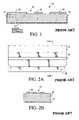
- a calibration substrate available from Cascade Microtech of Beaverton, Oreg.includes a set of calibration structures.
- the calibration structuresinclude a set of conductive members 54 supported by the substrate and spatially arranged across the substrate. Similar conductive members are aligned in an array orientation.
- a small portion of resistive material 56is located adjacent to the end of each of the conductive members.
- the wider conductive membersare approximately 525 microns wide and the thinner conductive members are approximately 100 microns wide, with a spacing of approximately 750 microns between conductive material columns.
- the resistive materialis approximately 150 microns in length and has a width equal to that of the conductive material.
- the conductive membersare approximately 1400 microns in length.
- the column of conductive members 60are for open calibration tests, the column of conductive member 62 are for load calibration tests, the column of conductive members 64 are for short calibration tests, the column of conductive members 66 are for through conductive tests, and the column of conductive members 68 are for loop back through conductive tests.
- the resulting structureincludes a resonance at approximately 33 giga-hertz having a magnitude of approximately 0.10-0.15 dB deviation from the ideal (0 dB) when measuring a short calibration structure (S 11 measurement), as shown in FIG. 4 .
- the S 11 magnitude in dBis calculated as 20*log(x), where x is the magnitude of the return signal with the input normalized to 1. This resonance makes probing of semiconductors more difficult in the general range of 33 giga-hertz because it is difficult to calibrate the system.
- Qis a measure of the sharpness of the resonant peak in the frequency response of the system and is inversely proportional to the damping in the system, and may be also considered the reactive portion over the resistive portion of the impedance causing the resonance.
- Q(center frequency in hertz)/(bandwidth (0.707 times down (3 dB reduction in magnitude) from the maximum magnitude at the center frequency)).
- the Q factor of the impedance causing the 33 GHz resonanceis approximately 22.
- FIG. 1is a cross-sectional view of a coplanar transmission structure.
- FIGS. 2A-Bare plan and cross-sectional views of coplanar stripline cases incorporating resistive layers.
- FIG. 3illustrates an existing calibration substrate.
- FIG. 4illustrates S 11 response of a short without resistive termination of the microstrip mode.
- FIG. 5illustrates a modified calibration substrate
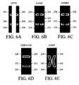
- FIGS. 6A-6Eillustrate calibration regions.
- FIG. 7illustrates a LC circuit
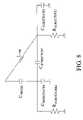
- FIG. 8illustrates a LCR circuit
- FIG. 9illustrates S 11 response of a short with resistive termination of the microstrip mode.
- FIG. 10illustrates a smith chart of the impedance matches of the probe impedance without resistive material.
- FIG. 11illustrates a smith chart of the impedance matches of the probe impedance with limited resistive material.
- FIG. 12illustrates another calibration structure.
- a calibration substratethat includes one or more conductive members is illustrated.
- the structures on the calibration substrateare modeled by the manufacturer with some degree of accuracy so that the probe, network analyzer, and cabling between the probe and network analyzer can be accurately modeled with some degree of precision.
- the preferred dimensionsinclude the wider conductive members being approximately 525 microns wide and the thinner conducive members being approximately 100 microns wide.
- the length of the conductorsare preferably 1400 microns.
- the column of conductive members 160are for open calibration tests, the column of conductive member 162 are for load calibration tests, the column of conductive members 164 are for short calibration tests, the column of conductive members 166 are for through conductive tests, and the column of conductive members 168 are for loop back through conductive tests.
- the signal pathsare located on the small conductive regions within each larger conductive region.
- the ground pathsare located on the larger conductive regions. In some cases, the signal and ground conductive portions are tied together. Referring to FIG.
- the open conductive test 160 for a dual path testincludes a pair of signal conductive regions 200 and 202 , and a ground conductive region 204 .
- the load conductive test 162 for a dual path testincludes a pair of signal conductive regions 210 and 212 , and a ground conductive region 214 , where the respective conductive regions 210 and 212 are interconnected by a resistive material 216 , such as a 50 ohm/square resistive material.
- the short conductive test 164 for a dual path testincludes a pair of signal conductive regions 220 and 222 , and a ground conductive region 224 which is electrically connected to the signal conductive regions 220 and 222 .
- the through conductive test 166 for a dual path testincludes a pair of signal conductive regions 230 and 232 , and a ground conductive region 234 .
- the loop back conductive test 168 for a dual path testincludes a pair of signal conductive regions 240 and 242 , and a ground conductive region 244 .
- the calibrationmay include any suitable technique, such as for example, line-reflect-match, short-open-load, through-reflect line, line-reflect-reflect-match, short-open-load-through, and short-open-load-reciprocal.
- Deviations from the ideal response of the probe/calibration substrate combinationare stored in the network analyzer and software algorithms may be used to compensate for these detected deviations as well as the non-ideal response of the network analyzer and the interface to the probe.
- the present inventorconsidered the effects of the resonance frequency occurring at approximately 33 GHz for the structure shown in FIG. 3 .
- the present inventorspeculated that one potential explanation for the observed effect is that there exists a significant capacitance “C structure ” between adjacent columns of calibration resistor/conductor/resistor structures.
- C probeanother significant capacitance between the probe itself and the adjacent calibration structure to the one being tested.
- the ground path of the probe tiphas a significant inductance L tip .
- the resulting pair of capacitances C structure and C probe together with the inductance L tipresult in a inductor-capacitor (LC) resonance structure.
- LCinductor-capacitor
- This LC resonance structurevaries by including additional probe tip inductance and additional mutual inductance between the probe tips when the substrate is used for calibration of a dual (or more) signal path probe.
- the probemay include a ground/signal/ground/signal/ground structure where the pair of signal paths may be located on different conductive members during calibration.
- the substratemay likewise be used for single port calibrations between a pair of probes or for a single probe or one to multiple ports. Further, in most cases the signal lines may be used for input or output or both.
- one techniquemay be to space the conductive members at locations further distant from one another. This results in a decrease in the capacitance between the conductive members. As the capacitance between the conductive members is decreased the resonance frequency of the effective LC circuit is increased. With sufficient increase in the resonance frequency, the resonance may occur at a frequency that is not of interest during measurement, such as above 200 giga-hertz. Unfortunately, increasing the spacing between the conductive members results in fewer calibration structures on the substrate, which become worn after repeated use.
- C probe and C structureadditionally couple to such resonators, which can further distort the desired signals.
- a resistive element 170should be included in the LC circuit to effectively provide an LCR circuit, as illustrated in FIG. 8 .
- the additional resistive element R structureis sufficient to dampen the resonance aspects of the structure to a sufficiently small level.
- the resistive elementinterconnects the two adjacent conductive elements. Measurements resulting from the modified structure show a deviation from ideal of less than 0.02 dB in a measurement of the short structure (S 11 measurement). In contrast, the previously existing structures that included resistive material did not have a sufficiently wide resistor area to reduce the resonance(s), whatever their origin.
- the present inventorspeculates that the narrow resistors of existing structures provide insufficient capacitance between the resistor material to the ground plane such that little current flows in the resistor material, thus resulting in a relatively high Q. Accordingly, the present inventor speculates that with additional resistor material or additional resistance sufficient capacitance exists between the resistive material and the ground plane so that sufficient current flows in the resistive material thus lowering the Q of the resonator structure created by the ground conductor.
- the modified structurehas a characteristic that was previously unobtainable with a loss of less than 0.05 dB between 5 GHz and 100 GHz, and more preferably between 10 GHz and 70 GHz, more preferably between 20 and 60 GHz, more preferably between 30 GHz and 50 GHz, or and more preferably a loss of less than 0.025 dB between these ranges (S 11 measurement).
- This measurementmay be characterized as the vector difference between the structure's S 11 and the S 11 of a relatively trusted short or open.
- the modified structurepermits the Q of the resonance to be substantially reduced, such as to a value less than 5, more preferably less than 3, more preferably less than 2, and more preferably less than approximately 1.
- the resistive materialis preferably connected to both of the conductive materials and extends the entire distance between the conductive materials, less resistive material may likewise be used, if desired.
- the resistive materialmay extend at least 50% of the distance between the conductive members, more preferably at least 75% of the distance between the conductive members, more preferably at least 90% of the distance between the conductive members, and more preferably at least 95% of the distance between the conductive members.
- resistive materialmay be included between the columns of conductive materials and extend the entire distance between the conductive materials.
- less resistive materialmay be included between the columns of conductive materials, if desired, and more preferably between the conductive materials.
- the resistive materialmay extend at least 50% of the distance between the conductive members, more preferably at least 75% of the distance between the conductive members, more preferably at least 90% of the distance between the conductive members, and more preferably at least 95% of the distance between the conductive members.
- the present inventorbased upon the aforementioned observation, considered that during the calibration process the probe maintains a signal primarily in a single mode, such as CPW mode (coplanar waveguide).
- CPW modecoplanar waveguide
- the signal propagating in the CPW modeis imposed on the calibration substrate.
- the majority of the signalis maintained in the CPW mode by the calibration substrate.
- a portion of the signal in the CPW modeis converted by the calibration structures into other modes, such as a microstrip mode between the conductive members and the bottom of the substrate.
- this mode conversion from CPW to microstripis substantial, such as 33 GHz as previously discussed.
- the resistor materialis terminating the microstrip mode in a resistance substantially equal to its characteristic impedance. If not connected to other conductors, the resistor area should be wide enough to create sufficient capacitance to the ground plane to cause the ground conductor to see an impedance substantially equal to the characteristic impedance of the undesired mode (within +/ ⁇ 25 percent, more preferably within +/ ⁇ 10 percent).
- the resistive materialpreferably has a resistance that is within +/ ⁇ 25 percent, more preferably within +/ ⁇ 10 percent, of the characteristic impedance of the microstrip mode.
- the length of the resistive materialis preferably sufficient to provide an impedance substantially equal to the characteristic impedance of the undesired mode, preferably within +/ ⁇ 10 percent, and preferably within +/ ⁇ 25 percent.
- the area of the resistive materialis preferably sufficient to provide an impedance substantially equal to the characteristic impedance of the undesired mode, preferably within +/ ⁇ 10 percent, and preferably within +/ ⁇ 25 percent.
- the thickness of the substrate and/or its dielectric constantis preferably sufficient such that the conductive region (ground conductor and/or signal conductor(s)) and/or resistive material has an impedance substantially equal to the characteristic impedance of the undesired mode, preferably within +/ ⁇ 10 percent, and preferably within +/ ⁇ 25 percent.
- the characteristic impedance of the microstrip mode to the ground planeis related to the ratio of the width of the microstrip (resistor and/or conductive region (ground conductor and/or signal conductor(s)) to the substrate thickness. Therefore, the resistive material may be considered as a very lossy microstrip line of similar impedance which preferably has a length substantially the same as the length of the ground conductor, within +/ ⁇ 10 percent, within +/ ⁇ 25 percent, within +/ ⁇ 50 percent, within +/ ⁇ 75 percent. If the resistive element is considered as a series of lumped elements, a longer resistive structure has more capacitance to the ground plane, thus providing a termination resistor.
- the resistive materialmay be of a length greater than 300 microns, more preferably greater than 500 microns, and more preferably greater than 750 microns.
- the resistive materialmay likewise have the same width as the conductive region, or within 75% of the same width.
- the resistive materialmay be characterized as having a total resistance (per side) of more than 40 ohms, more preferably more than 45 ohms, more preferably more than 50 ohms, and more preferably more than 55 ohms.
- the S 11 characteristics, Q value characteristics, resistive material characteristics, and reactive characteristicsmay be related to a single combination of a conductive member and resistive material without relation to other conductive members or other resistive members.
- the relationships described hereinmay be considered as is without regard to the type of resistive material used. Also, the relationships described herein are preferably for a resistive material of approximately 50 ohms/square (within +/ ⁇ 5 percent, within +/ ⁇ 10 percent, within +/ ⁇ 25 percent). However, if the resistance of the resistive material is other than 50 ohms/square then the width of the conductive region (ground conductors and/or signal conductors) and/or resistive material, thickness of the substrate, dielectric constant of the substrate, length of the conductive region (ground conductors and/or signal conductors) and/or resistive material, may be modified to maintain the same ratios and/or the same characteristic impedance matching.
- the substratemay include microwave absorbing material between the substrate and the chuck, if desired. Further, microwave absorbing material may be located on the sides and/or the top surface of the substrate, if desired. Also, the chuck may be, for example, conductive, non-conductive, lossy, supporting an upper dielectric layer, supporting an upper microwave absorbing material. In addition, the characteristics of the resistive material may likewise be included with conductive regions on a calibration substrates for a single channel, such as merely a ground region and a signal region.
- the resistive materialmay have different sheet resistances to match different application needs depending on the characteristic impedance of the device under test. Additionally patterning of the lossy material in various shapes may be chosen to meet specific application needs.
- FIG. 12Another calibration structure is shown in FIG. 12 suitable for membrane type probes available from Cascade Microtech, Inc. of Beaverton, Oreg.
- the structureincludes conductive regions, such as elongate ground conductors with a signal conductor between a pair of ground conductors separated by a gap or dielectric material.
- the conductive regionsare preferably spaced apart by gaps or dielectric material. Between different conductive regions may be dielectric or resistive material.
- the central regionincludes a large conductive region and individual pads for the probing contacts which may be electrically isolated form the large conductive region.
Landscapes
- Physics & Mathematics (AREA)
- General Physics & Mathematics (AREA)
- Engineering & Computer Science (AREA)
- General Engineering & Computer Science (AREA)
- Computer Hardware Design (AREA)
- Microelectronics & Electronic Packaging (AREA)
- Power Engineering (AREA)
- Condensed Matter Physics & Semiconductors (AREA)
- Measurement Of Resistance Or Impedance (AREA)
- Testing Or Measuring Of Semiconductors Or The Like (AREA)
- Tests Of Electronic Circuits (AREA)
- Measuring Leads Or Probes (AREA)
- Investigating Or Analysing Materials By Optical Means (AREA)
- Sampling And Sample Adjustment (AREA)
- Investigating Or Analyzing Materials By The Use Of Ultrasonic Waves (AREA)
Abstract
Description
Claims (5)
Priority Applications (10)
| Application Number | Priority Date | Filing Date | Title |
|---|---|---|---|
| US10/794,246US7250626B2 (en) | 2003-10-22 | 2004-03-05 | Probe testing structure |
| GB0608025AGB2423588B (en) | 2003-10-22 | 2004-09-15 | Probe testing structure |
| EP04784414AEP1680813A2 (en) | 2003-10-22 | 2004-09-15 | Probe testing structure |
| DE202004021017UDE202004021017U1 (en) | 2003-10-22 | 2004-09-15 | Probe calibrating substrate for electronic application, has two conductive units interconnected with two respective ground paths of probes, where resistive material extends certain percentage of distance between units |
| PCT/US2004/030545WO2005043176A2 (en) | 2003-10-22 | 2004-09-15 | Probe testing structure |
| KR1020067008509AKR20060096496A (en) | 2003-10-22 | 2004-09-15 | Probe test structure |
| JP2006536629AJP2007509343A (en) | 2003-10-22 | 2004-09-15 | Probe test structure |
| DE112004002022TDE112004002022T5 (en) | 2003-10-22 | 2004-09-15 | Measuring probe test structure |
| TW093132073ATW200517668A (en) | 2003-10-22 | 2004-10-22 | Probe testing structure |
| US11/820,877US8069491B2 (en) | 2003-10-22 | 2007-06-20 | Probe testing structure |
Applications Claiming Priority (2)
| Application Number | Priority Date | Filing Date | Title |
|---|---|---|---|
| US51366303P | 2003-10-22 | 2003-10-22 | |
| US10/794,246US7250626B2 (en) | 2003-10-22 | 2004-03-05 | Probe testing structure |
Related Child Applications (1)
| Application Number | Title | Priority Date | Filing Date |
|---|---|---|---|
| US11/820,877ContinuationUS8069491B2 (en) | 2003-10-22 | 2007-06-20 | Probe testing structure |
Publications (2)
| Publication Number | Publication Date |
|---|---|
| US20050088191A1 US20050088191A1 (en) | 2005-04-28 |
| US7250626B2true US7250626B2 (en) | 2007-07-31 |
Family
ID=34526887
Family Applications (2)
| Application Number | Title | Priority Date | Filing Date |
|---|---|---|---|
| US10/794,246Expired - LifetimeUS7250626B2 (en) | 2003-10-22 | 2004-03-05 | Probe testing structure |
| US11/820,877Expired - Fee RelatedUS8069491B2 (en) | 2003-10-22 | 2007-06-20 | Probe testing structure |
Family Applications After (1)
| Application Number | Title | Priority Date | Filing Date |
|---|---|---|---|
| US11/820,877Expired - Fee RelatedUS8069491B2 (en) | 2003-10-22 | 2007-06-20 | Probe testing structure |
Country Status (8)
| Country | Link |
|---|---|
| US (2) | US7250626B2 (en) |
| EP (1) | EP1680813A2 (en) |
| JP (1) | JP2007509343A (en) |
| KR (1) | KR20060096496A (en) |
| DE (2) | DE112004002022T5 (en) |
| GB (1) | GB2423588B (en) |
| TW (1) | TW200517668A (en) |
| WO (1) | WO2005043176A2 (en) |
Cited By (4)
| Publication number | Priority date | Publication date | Assignee | Title |
|---|---|---|---|---|
| US7969173B2 (en) | 2000-09-05 | 2011-06-28 | Cascade Microtech, Inc. | Chuck for holding a device under test |
| US8069491B2 (en)* | 2003-10-22 | 2011-11-29 | Cascade Microtech, Inc. | Probe testing structure |
| US8319503B2 (en) | 2008-11-24 | 2012-11-27 | Cascade Microtech, Inc. | Test apparatus for measuring a characteristic of a device under test |
| US8614508B2 (en) | 2011-09-21 | 2013-12-24 | Stats Chippac Ltd. | Integrated circuit system with test pads and method of manufacture thereof |
Families Citing this family (27)
| Publication number | Priority date | Publication date | Assignee | Title |
|---|---|---|---|---|
| US6232789B1 (en) | 1997-05-28 | 2001-05-15 | Cascade Microtech, Inc. | Probe holder for low current measurements |
| DE20114544U1 (en) | 2000-12-04 | 2002-02-21 | Cascade Microtech, Inc., Beaverton, Oreg. | wafer probe |
| KR100864916B1 (en) | 2002-05-23 | 2008-10-22 | 캐스케이드 마이크로테크 인코포레이티드 | Probes for Testing Devices Under Test |
| US6724205B1 (en) | 2002-11-13 | 2004-04-20 | Cascade Microtech, Inc. | Probe for combined signals |
| US7057404B2 (en) | 2003-05-23 | 2006-06-06 | Sharp Laboratories Of America, Inc. | Shielded probe for testing a device under test |
| WO2005065258A2 (en) | 2003-12-24 | 2005-07-21 | Cascade Microtech, Inc. | Active wafer probe |
| EP1789812A2 (en) | 2004-09-13 | 2007-05-30 | Cascade Microtech, Inc. | Double sided probing structures |
| US7449899B2 (en) | 2005-06-08 | 2008-11-11 | Cascade Microtech, Inc. | Probe for high frequency signals |
| JP5080459B2 (en) | 2005-06-13 | 2012-11-21 | カスケード マイクロテック インコーポレイテッド | Wideband active / passive differential signal probe |
| US7609077B2 (en)* | 2006-06-09 | 2009-10-27 | Cascade Microtech, Inc. | Differential signal probe with integral balun |
| US7443186B2 (en) | 2006-06-12 | 2008-10-28 | Cascade Microtech, Inc. | On-wafer test structures for differential signals |
| US7403028B2 (en) | 2006-06-12 | 2008-07-22 | Cascade Microtech, Inc. | Test structure and probe for differential signals |
| US7764072B2 (en) | 2006-06-12 | 2010-07-27 | Cascade Microtech, Inc. | Differential signal probing system |
| US7723999B2 (en)* | 2006-06-12 | 2010-05-25 | Cascade Microtech, Inc. | Calibration structures for differential signal probing |
| WO2008021907A2 (en)* | 2006-08-08 | 2008-02-21 | Tektronix, Inc. | Calibrated s-parameter measurements of probes |
| US7876114B2 (en) | 2007-08-08 | 2011-01-25 | Cascade Microtech, Inc. | Differential waveguide probe |
| KR100808816B1 (en)* | 2007-08-10 | 2008-03-03 | 주식회사 파이컴 | Electrical contact assembly and electrical inspection device comprising same |
| CN101872002B (en)* | 2010-05-28 | 2016-01-20 | 上海华虹宏力半导体制造有限公司 | Probe detection device and method thereof |
| US9000989B2 (en)* | 2011-08-17 | 2015-04-07 | Apple Inc. | Test system with adjustable radio-frequency probe array |
| JP5900019B2 (en)* | 2012-02-29 | 2016-04-06 | 日亜化学工業株式会社 | Light emitting device holder |
| TWI526132B (en)* | 2013-12-13 | 2016-03-11 | Mpi Corp | Correction film structure |
| US9432064B2 (en)* | 2014-02-11 | 2016-08-30 | Introbotics Corporation | System and method for automated loss testing |
| TWI509259B (en)* | 2014-03-18 | 2015-11-21 | Nat Applied Res Laboratories | Conductive type current probe |
| US10180486B2 (en)* | 2016-03-16 | 2019-01-15 | Formfactor Beaverton, Inc. | Test standards and methods for impedance calibration of a probe system, and probe systems that include the test standards or utilize the methods |
| TWI750683B (en)* | 2020-06-02 | 2021-12-21 | 緯穎科技服務股份有限公司 | Signal testing device and signal testing method |
| US11943886B2 (en)* | 2020-11-11 | 2024-03-26 | Te Connectivity Solutions Gmbh | Electronic assembly including a compression assembly for cable connector modules |
| TWI747750B (en)* | 2021-02-25 | 2021-11-21 | 元智大學 | Calibration structure and calibration method for double-sided probing measurement |
Citations (511)
| Publication number | Priority date | Publication date | Assignee | Title |
|---|---|---|---|---|
| US1337866A (en) | 1917-09-27 | 1920-04-20 | Griffiths Ethel Grace | System for protecting electric cables |
| US2142625A (en) | 1932-07-06 | 1939-01-03 | Hollandsche Draad En Kabelfab | High tension cable |
| US2197081A (en) | 1937-06-14 | 1940-04-16 | Transit Res Corp | Motor support |
| US2376101A (en) | 1942-04-01 | 1945-05-15 | Ferris Instr Corp | Electrical energy transmission |
| US2389668A (en) | 1943-03-04 | 1945-11-27 | Barnes Drill Co | Indexing mechanism for machine tables |
| US2471897A (en) | 1945-01-13 | 1949-05-31 | Trico Products Corp | Fluid motor packing |
| US2812502A (en) | 1953-07-07 | 1957-11-05 | Bell Telephone Labor Inc | Transposed coaxial conductor system |
| US3176091A (en) | 1962-11-07 | 1965-03-30 | Helmer C Hanson | Controlled multiple switching unit |
| US3185927A (en) | 1961-01-31 | 1965-05-25 | Kulicke & Soffa Mfg Co | Probe instrument for inspecting semiconductor wafers including means for marking defective zones |
| US3193712A (en) | 1962-03-21 | 1965-07-06 | Clarence A Harris | High voltage cable |
| US3192844A (en) | 1963-03-05 | 1965-07-06 | Kulicke And Soffa Mfg Company | Mask alignment fixture |
| US3201721A (en) | 1963-12-30 | 1965-08-17 | Western Electric Co | Coaxial line to strip line connector |
| US3230299A (en) | 1962-07-18 | 1966-01-18 | Gen Cable Corp | Electrical cable with chemically bonded rubber layers |
| US3256484A (en) | 1962-09-10 | 1966-06-14 | Tektronix Inc | High voltage test probe containing a part gas, part liquid dielectric fluid under pressure and having a transparent housing section for viewing the presence of the liquid therein |
| US3265969A (en) | 1960-04-19 | 1966-08-09 | Ipa Anstalt | High voltage probe apparatus with a plurality of discharge tube isolating spark gaps therein |
| US3289046A (en) | 1964-05-19 | 1966-11-29 | Gen Electric | Component chip mounted on substrate with heater pads therebetween |
| US3333274A (en) | 1965-04-21 | 1967-07-25 | Micro Tech Mfg Inc | Testing device |
| US3405361A (en) | 1964-01-08 | 1968-10-08 | Signetics Corp | Fluid actuable multi-point microprobe for semiconductors |
| US3408565A (en) | 1966-03-02 | 1968-10-29 | Philco Ford Corp | Apparatus for sequentially testing electrical components under controlled environmental conditions including a component support mating test head |
| US3435185A (en) | 1966-01-11 | 1969-03-25 | Rohr Corp | Sliding vacuum seal for electron beam welder |
| US3484679A (en) | 1966-10-03 | 1969-12-16 | North American Rockwell | Electrical apparatus for changing the effective capacitance of a cable |
| US3596228A (en) | 1969-05-29 | 1971-07-27 | Ibm | Fluid actuated contactor |
| US3602845A (en) | 1970-01-27 | 1971-08-31 | Us Army | Slot line nonreciprocal phase shifter |
| US3609539A (en) | 1968-09-28 | 1971-09-28 | Ibm | Self-aligning kelvin probe |
| US3648169A (en) | 1969-05-26 | 1972-03-07 | Teledyne Inc | Probe and head assembly |
| US3654573A (en) | 1970-06-29 | 1972-04-04 | Bell Telephone Labor Inc | Microwave transmission line termination |
| US3662318A (en) | 1970-12-23 | 1972-05-09 | Comp Generale Electricite | Transition device between coaxial and microstrip lines |
| US3710251A (en) | 1971-04-07 | 1973-01-09 | Collins Radio Co | Microelectric heat exchanger pedestal |
| US3714572A (en) | 1970-08-21 | 1973-01-30 | Rca Corp | Alignment and test fixture apparatus |
| US3775644A (en) | 1972-09-20 | 1973-11-27 | Communications Satellite Corp | Adjustable microstrip substrate holder |
| US3777260A (en) | 1972-12-14 | 1973-12-04 | Ibm | Grid for making electrical contact |
| US3810017A (en) | 1972-05-15 | 1974-05-07 | Teledyne Inc | Precision probe for testing micro-electronic units |
| US3814888A (en) | 1971-11-19 | 1974-06-04 | Gen Electric | Solid state induction cooking appliance |
| US3829076A (en) | 1972-06-08 | 1974-08-13 | H Sofy | Dial index machine |
| US3863181A (en) | 1973-12-03 | 1975-01-28 | Bell Telephone Labor Inc | Mode suppressor for strip transmission lines |
| US3866093A (en) | 1972-09-18 | 1975-02-11 | Norbert L Kusters | Low leakage electrical power input circuit for electromedical and other similar apparatus |
| US3930809A (en) | 1973-08-21 | 1976-01-06 | Wentworth Laboratories, Inc. | Assembly fixture for fixed point probe card |
| US3936743A (en) | 1974-03-05 | 1976-02-03 | Electroglas, Inc. | High speed precision chuck assembly |
| US3970934A (en) | 1974-08-12 | 1976-07-20 | Akin Aksu | Printed circuit board testing means |
| US3996517A (en) | 1975-12-29 | 1976-12-07 | Monsanto Company | Apparatus for wafer probing having surface level sensing |
| US4001685A (en) | 1974-03-04 | 1977-01-04 | Electroglas, Inc. | Micro-circuit test probe |
| US4009456A (en) | 1970-10-07 | 1977-02-22 | General Microwave Corporation | Variable microwave attenuator |
| US4008900A (en) | 1976-03-15 | 1977-02-22 | John Freedom | Indexing chuck |
| US4027253A (en) | 1973-05-18 | 1977-05-31 | Societe Lignes Telegraphiques Et Telephoniques | Non-reciprocal broadband slot line device |
| US4035723A (en) | 1975-10-16 | 1977-07-12 | Xynetics, Inc. | Probe arm |
| US4038894A (en) | 1975-07-18 | 1977-08-02 | Springfield Tool And Die, Inc. | Piercing apparatus |
| US4042119A (en) | 1975-06-30 | 1977-08-16 | International Business Machines Corporation | Workpiece positioning apparatus |
| US4049252A (en) | 1976-02-04 | 1977-09-20 | Bell Theodore F | Index table |
| US4093988A (en) | 1976-11-08 | 1978-06-06 | General Electric Company | High speed frequency response measurement |
| US4099120A (en) | 1976-04-19 | 1978-07-04 | Akin Aksu | Probe head for testing printed circuit boards |
| US4115735A (en) | 1976-10-14 | 1978-09-19 | Faultfinders, Inc. | Test fixture employing plural platens for advancing some or all of the probes of the test fixture |
| US4115736A (en) | 1977-03-09 | 1978-09-19 | The United States Of America As Represented By The Secretary Of The Air Force | Probe station |
| US4116523A (en) | 1976-01-23 | 1978-09-26 | James M. Foster | High frequency probe |
| JPS5352354Y2 (en) | 1974-05-23 | 1978-12-14 | ||
| US4151465A (en) | 1977-05-16 | 1979-04-24 | Lenz Seymour S | Variable flexure test probe for microelectronic circuits |
| US4161692A (en) | 1977-07-18 | 1979-07-17 | Cerprobe Corporation | Probe device for integrated circuit wafers |
| US4172993A (en) | 1978-09-13 | 1979-10-30 | The Singer Company | Environmental hood for testing printed circuit cards |
| WO1980000101A1 (en) | 1978-06-21 | 1980-01-24 | Cerprobe Corp | Probe and interface device for integrated circuit wafers |
| US4186338A (en) | 1976-12-16 | 1980-01-29 | Genrad, Inc. | Phase change detection method of and apparatus for current-tracing the location of faults on printed circuit boards and similar systems |
| DE2912826A1 (en) | 1979-03-30 | 1980-10-16 | Heinz Laass | Compact pair of electrical probes packaged for portability - are used for voltage or short circuit testing and clamped together, when not in use, by magnets |
| JPS567439Y2 (en) | 1975-09-20 | 1981-02-18 | ||
| US4275446A (en) | 1978-11-13 | 1981-06-23 | Siemens Aktiengesellschaft | Method and apparatus for measurement of attenuation and distortion by a test object |
| US4280112A (en) | 1979-02-21 | 1981-07-21 | Eisenhart Robert L | Electrical coupler |
| US4284033A (en) | 1979-10-31 | 1981-08-18 | Rca Corporation | Means to orbit and rotate target wafers supported on planet member |
| US4284682A (en) | 1980-04-30 | 1981-08-18 | Nasa | Heat sealable, flame and abrasion resistant coated fabric |
| US4287473A (en) | 1979-05-25 | 1981-09-01 | The United States Of America As Represented By The United States Department Of Energy | Nondestructive method for detecting defects in photodetector and solar cell devices |
| US4342958A (en) | 1980-03-28 | 1982-08-03 | Honeywell Information Systems Inc. | Automatic test equipment test probe contact isolation detection method |
| US4346355A (en) | 1980-11-17 | 1982-08-24 | Raytheon Company | Radio frequency energy launcher |
| US4352061A (en) | 1979-05-24 | 1982-09-28 | Fairchild Camera & Instrument Corp. | Universal test fixture employing interchangeable wired personalizers |
| US4357575A (en) | 1980-06-17 | 1982-11-02 | Dit-Mco International Corporation | Apparatus for use in testing printed circuit process boards having means for positioning such boards in proper juxtaposition with electrical contacting assemblies |
| DE3125552C1 (en) | 1981-06-29 | 1982-11-11 | Siemens AG, 1000 Berlin und 8000 München | Tester indicating voltage magnitude, polarity and testing continuity - has mains section and switchable reservoir enabling self-testing |
| US4365195A (en) | 1979-12-27 | 1982-12-21 | Communications Satellite Corporation | Coplanar waveguide mounting structure and test fixture for microwave integrated circuits |
| US4365109A (en) | 1980-01-25 | 1982-12-21 | The United States Of America As Represented By The Secretary Of The Air Force | Coaxial cable design |
| US4371742A (en) | 1977-12-20 | 1983-02-01 | Graham Magnetics, Inc. | EMI-Suppression from transmission lines |
| US4376920A (en) | 1981-04-01 | 1983-03-15 | Smith Kenneth L | Shielded radio frequency transmission cable |
| US4383178A (en) | 1980-04-11 | 1983-05-10 | Hitachi, Ltd. | System for driving rotary member in vacuum |
| US4414638A (en) | 1981-04-30 | 1983-11-08 | Dranetz Engineering Laboratories, Inc. | Sampling network analyzer with stored correction of gain errors |
| US4419626A (en) | 1981-08-25 | 1983-12-06 | Daymarc Corporation | Broad band contactor assembly for testing integrated circuit devices |
| US4425395A (en) | 1981-04-30 | 1984-01-10 | Fujikura Rubber Works, Ltd. | Base fabrics for polyurethane-coated fabrics, polyurethane-coated fabrics and processes for their production |
| US4426619A (en) | 1981-06-03 | 1984-01-17 | Temptronic Corporation | Electrical testing system including plastic window test chamber and method of using same |
| US4480223A (en) | 1981-11-25 | 1984-10-30 | Seiichiro Aigo | Unitary probe assembly |
| US4479690A (en) | 1982-09-13 | 1984-10-30 | The United States Of America As Represented By The Secretary Of The Navy | Underwater splice for submarine coaxial cable |
| US4487996A (en) | 1982-12-02 | 1984-12-11 | Electric Power Research Institute, Inc. | Shielded electrical cable |
| US4491173A (en) | 1982-05-28 | 1985-01-01 | Temptronic Corporation | Rotatable inspection table |
| US4503335A (en) | 1981-04-13 | 1985-03-05 | Canon Kabushiki Kaisha | Semiconductor printing apparatus with multiple independent temperature control |
| US4507602A (en) | 1982-08-13 | 1985-03-26 | The United States Of America As Represented By The Secretary Of The Air Force | Measurement of permittivity and permeability of microwave materials |
| JPS6071425U (en) | 1983-10-25 | 1985-05-20 | 株式会社アマダ | Mounting structure of upper apron in press machine |
| EP0087497A3 (en) | 1982-02-15 | 1985-07-03 | Spencer Products Company | Tape measure |
| US4528504A (en) | 1982-05-27 | 1985-07-09 | Harris Corporation | Pulsed linear integrated circuit tester |
| US4532423A (en) | 1982-05-31 | 1985-07-30 | Tokyo Shibaura Denki Kabushiki Kaisha | IC Tester using an electron beam capable of easily setting a probe card unit for wafers & packaged IC's to be tested |
| US4531474A (en) | 1983-06-04 | 1985-07-30 | Dainippon Screen Manufacturing Co., Ltd. | Rotary board treating apparatus |
| US4557599A (en) | 1984-03-06 | 1985-12-10 | General Signal Corporation | Calibration and alignment target plate |
| US4567321A (en) | 1984-02-20 | 1986-01-28 | Junkosha Co., Ltd. | Flexible flat cable |
| US4566184A (en) | 1981-08-24 | 1986-01-28 | Rockwell International Corporation | Process for making a probe for high speed integrated circuits |
| US4567908A (en) | 1983-05-31 | 1986-02-04 | Contraves Ag | Discharge system and method of operating same |
| US4575676A (en) | 1983-04-04 | 1986-03-11 | Advanced Research And Applications Corporation | Method and apparatus for radiation testing of electron devices |
| US4588970A (en) | 1984-01-09 | 1986-05-13 | Hewlett-Packard Company | Three section termination for an R.F. triaxial directional bridge |
| US4621169A (en) | 1983-06-21 | 1986-11-04 | Compagnie Francaise De Raffinage | Electric cable construction and uses therefor |
| US4626618A (en) | 1984-05-08 | 1986-12-02 | Fujikura Ltd. | DC electric power cable |
| WO1986007493A1 (en)* | 1985-06-13 | 1986-12-18 | Plessey Overseas Limited | Calibration apparatus for integrated circuits |
| US4642417A (en) | 1984-07-30 | 1987-02-10 | Kraftwerk Union Aktiengesellschaft | Concentric three-conductor cable |
| US4646005A (en) | 1984-03-16 | 1987-02-24 | Motorola, Inc. | Signal probe |
| JPS6211243B2 (en) | 1982-12-14 | 1987-03-11 | Matsushita Electric Ind Co Ltd | |
| US4665360A (en) | 1985-03-11 | 1987-05-12 | Eaton Corporation | Docking apparatus |
| US4673839A (en) | 1986-09-08 | 1987-06-16 | Tektronix, Inc. | Piezoelectric pressure sensing apparatus for integrated circuit testing stations |
| US4675600A (en) | 1984-05-17 | 1987-06-23 | Geo International Corporation | Testing apparatus for plated through-holes on printed circuit boards, and probe therefor |
| US4680538A (en) | 1985-01-15 | 1987-07-14 | Cornell Research Foundation, Inc. | Millimeter wave vector network analyzer |
| US4684883A (en) | 1985-05-13 | 1987-08-04 | American Telephone And Telegraph Company, At&T Bell Laboratories | Method of manufacturing high-quality semiconductor light-emitting devices |
| US4691831A (en) | 1984-06-25 | 1987-09-08 | Takeda Riken Co., Ltd. | IC test equipment |
| US4694245A (en) | 1984-09-07 | 1987-09-15 | Precision Drilling, Inc. | Vacuum-actuated top access test probe fixture |
| US4695794A (en) | 1985-05-31 | 1987-09-22 | Santa Barbara Research Center | Voltage calibration in E-beam probe using optical flooding |
| US4697143A (en) | 1984-04-30 | 1987-09-29 | Cascade Microtech, Inc. | Wafer probe |
| US4703433A (en) | 1984-01-09 | 1987-10-27 | Hewlett-Packard Company | Vector network analyzer with integral processor |
| US4711563A (en) | 1987-02-11 | 1987-12-08 | Lass Bennett D | Portable collapsible darkroom |
| US4712370A (en) | 1986-04-24 | 1987-12-15 | The United States Of America As Represented By The Secretary Of The Air Force | Sliding duct seal |
| US4727637A (en) | 1987-01-20 | 1988-03-01 | The Boeing Company | Computer aided connector assembly method and apparatus |
| US4730158A (en) | 1986-06-06 | 1988-03-08 | Santa Barbara Research Center | Electron-beam probing of photodiodes |
| US4731577A (en) | 1987-03-05 | 1988-03-15 | Logan John K | Coaxial probe card |
| US4734872A (en) | 1985-04-30 | 1988-03-29 | Temptronic Corporation | Temperature control for device under test |
| US4739259A (en) | 1986-08-01 | 1988-04-19 | Tektronix, Inc. | Telescoping pin probe |
| US4744041A (en) | 1985-03-04 | 1988-05-10 | International Business Machines Corporation | Method for testing DC motors |
| GB2197081A (en) | 1986-11-07 | 1988-05-11 | Plessey Co Plc | Coplanar waveguide probe |
| US4755746A (en) | 1985-04-24 | 1988-07-05 | Prometrix Corporation | Apparatus and methods for semiconductor wafer testing |
| US4755874A (en) | 1987-08-31 | 1988-07-05 | Kla Instruments Corporation | Emission microscopy system |
| US4757255A (en) | 1986-03-03 | 1988-07-12 | National Semiconductor Corporation | Environmental box for automated wafer probing |
| US4758785A (en) | 1986-09-03 | 1988-07-19 | Tektronix, Inc. | Pressure control apparatus for use in an integrated circuit testing station |
| US4759712A (en) | 1986-10-17 | 1988-07-26 | Temptronic Corporation | Device for applying controlled temperature stimuli to nerve sensitive tissue |
| US4771234A (en) | 1986-11-20 | 1988-09-13 | Hewlett-Packard Company | Vacuum actuated test fixture |
| US4772846A (en) | 1986-12-29 | 1988-09-20 | Hughes Aircraft Company | Wafer alignment and positioning apparatus for chip testing by voltage contrast electron microscopy |
| JPS63143814U (en) | 1987-03-12 | 1988-09-21 | ||
| US4777434A (en) | 1985-10-03 | 1988-10-11 | Amp Incorporated | Microelectronic burn-in system |
| JPS63160355U (en) | 1987-04-08 | 1988-10-20 | ||
| US4783625A (en) | 1986-08-21 | 1988-11-08 | Tektronix, Inc. | Wideband high impedance card mountable probe |
| US4784213A (en) | 1986-04-08 | 1988-11-15 | Temptronic Corporation | Mixing valve air source |
| US4786867A (en) | 1986-09-02 | 1988-11-22 | Canon Kabushiki Kaisha | Wafer prober |
| US4787752A (en) | 1986-10-24 | 1988-11-29 | Fts Systems, Inc. | Live component temperature conditioning device providing fast temperature variations |
| US4791363A (en) | 1987-09-28 | 1988-12-13 | Logan John K | Ceramic microstrip probe blade |
| US4810981A (en) | 1987-06-04 | 1989-03-07 | General Microwave Corporation | Assembly of microwave components |
| US4812754A (en) | 1987-01-07 | 1989-03-14 | Tracy Theodore A | Circuit board interfacing apparatus |
| US4816767A (en) | 1984-01-09 | 1989-03-28 | Hewlett-Packard Company | Vector network analyzer with integral processor |
| US4818169A (en) | 1985-05-17 | 1989-04-04 | Schram Richard R | Automated wafer inspection system |
| US4827211A (en) | 1987-01-30 | 1989-05-02 | Cascade Microtech, Inc. | Wafer probe |
| EP0314481A1 (en) | 1987-10-28 | 1989-05-03 | Irish Transformers Limited | A temperature control instrument for electronic components under test |
| WO1989004001A1 (en) | 1987-10-27 | 1989-05-05 | Martin Marietta Corporation | Calibrating method for apparatus evaluating microwave/millimeter wave circuits |
| US4839587A (en) | 1988-03-29 | 1989-06-13 | Digital Equipment Corporation | Test fixture for tab circuits and devices |
| US4838802A (en) | 1987-07-08 | 1989-06-13 | Tektronix, Inc. | Low inductance ground lead |
| JPH01165968A (en) | 1987-12-22 | 1989-06-29 | Mitsubishi Electric Corp | Wafer probing apparatus |
| US4845426A (en) | 1987-05-20 | 1989-07-04 | Signatone Corporation | Temperature conditioner for tests of unpackaged semiconductors |
| US4849689A (en) | 1988-11-04 | 1989-07-18 | Cascade Microtech, Inc. | Microwave wafer probe having replaceable probe tip |
| US4858160A (en) | 1988-03-18 | 1989-08-15 | Cascade Microtech, Inc. | System for setting reference reactance for vector corrected measurements |
| US4856426A (en) | 1984-05-26 | 1989-08-15 | Heidelberger Druckmaschinen Ag | Sheet-fed rotary printing machine with printing units arranged in tandem |
| US4856904A (en) | 1985-01-21 | 1989-08-15 | Nikon Corporation | Wafer inspecting apparatus |
| US4859989A (en) | 1987-12-01 | 1989-08-22 | W. L. Gore & Associates, Inc. | Security system and signal carrying member thereof |
| JPH01209380A (en) | 1988-02-16 | 1989-08-23 | Fujitsu Ltd | Probe card |
| JPH01214038A (en) | 1988-02-22 | 1989-08-28 | Mitsubishi Electric Corp | probe card |
| JPH01219575A (en) | 1988-02-27 | 1989-09-01 | Anritsu Corp | High frequency characteristic measuring instrument |
| US4871883A (en) | 1986-07-29 | 1989-10-03 | W. L. Gore & Associates, Inc. | Electro-magnetic shielding |
| US4871965A (en) | 1987-03-16 | 1989-10-03 | Apex Microtechnology Corporation | Environmental testing facility for electronic components |
| US4884206A (en) | 1984-12-21 | 1989-11-28 | Bendix Electronics S.A. | Process and processing circuit for the analog output signal of a sensor |
| US4884026A (en) | 1987-06-24 | 1989-11-28 | Tokyo Electron Limited | Electrical characteristic measuring apparatus |
| JPH01296167A (en) | 1988-05-24 | 1989-11-29 | Mitsubishi Electric Corp | Probe card |
| US4888550A (en) | 1981-09-14 | 1989-12-19 | Texas Instruments Incorporated | Intelligent multiprobe tip |
| JPH01178872U (en) | 1988-06-04 | 1989-12-21 | ||
| US4894612A (en) | 1987-08-13 | 1990-01-16 | Hypres, Incorporated | Soft probe for providing high speed on-wafer connections to a circuit |
| US4893914A (en) | 1988-10-12 | 1990-01-16 | The Micromanipulator Company, Inc. | Test station |
| US4896109A (en) | 1987-12-07 | 1990-01-23 | The United States Of America As Represented By The Department Of Energy | Photoconductive circuit element reflectometer |
| US4899998A (en) | 1987-11-10 | 1990-02-13 | Hiroshi Teramachi | Rotational positioning device |
| US4904935A (en) | 1988-11-14 | 1990-02-27 | Eaton Corporation | Electrical circuit board text fixture having movable platens |
| US4904933A (en) | 1986-09-08 | 1990-02-27 | Tektronix, Inc. | Integrated circuit probe station |
| US4906920A (en) | 1988-10-11 | 1990-03-06 | Hewlett-Packard Company | Self-leveling membrane probe |
| US4916398A (en) | 1988-12-21 | 1990-04-10 | Spectroscopy Imaging Systems Corp. | Efficient remote transmission line probe tuning for NMR apparatus |
| US4918374A (en) | 1988-10-05 | 1990-04-17 | Applied Precision, Inc. | Method and apparatus for inspecting integrated circuit probe cards |
| US4918279A (en) | 1987-08-28 | 1990-04-17 | Charmilles Technologies, S.A. | EDM cutting machine including device for preventing transmission of sealing plate movement to guide head arm |
| US4923407A (en) | 1989-10-02 | 1990-05-08 | Tektronix, Inc. | Adjustable low inductance probe |
| US4926118A (en) | 1988-02-22 | 1990-05-15 | Sym-Tek Systems, Inc. | Test station |
| US4933634A (en) | 1988-01-22 | 1990-06-12 | Commissariat A L'energie Atomique | Device and method to measure a short radiation pulse or an electric pulse |
| JPH0222873Y2 (en) | 1981-02-09 | 1990-06-20 | ||
| JPH0222837Y2 (en) | 1983-12-26 | 1990-06-20 | ||
| JPH02220453A (en) | 1989-02-21 | 1990-09-03 | Nippon Telegr & Teleph Corp <Ntt> | Apparatus for inspecting electronic circuit on wafer |
| US4968931A (en) | 1989-11-03 | 1990-11-06 | Motorola, Inc. | Apparatus and method for burning in integrated circuit wafers |
| US4978907A (en) | 1989-05-10 | 1990-12-18 | At&T Bell Laboratories | Apparatus and method for expanding the frequency range over which electrical signal amplitudes can be accurately measured |
| US4978914A (en) | 1988-03-15 | 1990-12-18 | Furukawa Denki Kogyo Kabushiki Kaisha | Laminated board for testing electronic components |
| US4982153A (en) | 1989-02-06 | 1991-01-01 | Cray Research, Inc. | Method and apparatus for cooling an integrated circuit chip during testing |
| US4994737A (en) | 1990-03-09 | 1991-02-19 | Cascade Microtech, Inc. | System for facilitating planar probe measurements of high-speed interconnect structures |
| US5001423A (en) | 1990-01-24 | 1991-03-19 | International Business Machines Corporation | Dry interface thermal chuck temperature control system for semiconductor wafer testing |
| US5010296A (en) | 1989-12-13 | 1991-04-23 | Mitsubishi Denki Kabushiki Kaisha | Wafer prober |
| US5019692A (en) | 1990-03-29 | 1991-05-28 | Eastman Kodak Company | Thermostatic device for fuser |
| US5030907A (en) | 1989-05-19 | 1991-07-09 | Knights Technology, Inc. | CAD driven microprobe integrated circuit tester |
| US5034688A (en) | 1988-05-05 | 1991-07-23 | Ets Gourdon | Temperature conditioning support for small objects such as semi-conductor components and thermal regulation process using said support |
| JPH03175367A (en) | 1989-12-04 | 1991-07-30 | Sharp Corp | Measuring jig for dc characteristic of semiconductor device |
| US5041782A (en) | 1989-09-20 | 1991-08-20 | Design Technique International, Inc. | Microstrip probe |
| US5045781A (en) | 1989-06-08 | 1991-09-03 | Cascade Microtech, Inc. | High-frequency active probe having replaceable contact needles |
| JPH0367187B2 (en) | 1984-04-17 | 1991-10-22 | Nissan Motor | |
| US5061823A (en) | 1990-07-13 | 1991-10-29 | W. L. Gore & Associates, Inc. | Crush-resistant coaxial transmission line |
| US5065089A (en) | 1990-06-01 | 1991-11-12 | Tovex Tech, Inc. | Circuit handler with sectioned rail |
| US5065092A (en) | 1990-05-14 | 1991-11-12 | Triple S Engineering, Inc. | System for locating probe tips on an integrated circuit probe card and method therefor |
| US5066357A (en) | 1990-01-11 | 1991-11-19 | Hewlett-Packard Company | Method for making flexible circuit card with laser-contoured vias and machined capacitors |
| US5070297A (en) | 1990-06-04 | 1991-12-03 | Texas Instruments Incorporated | Full wafer integrated circuit testing device |
| US5077523A (en) | 1989-11-03 | 1991-12-31 | John H. Blanz Company, Inc. | Cryogenic probe station having movable chuck accomodating variable thickness probe cards |
| JPH04732Y2 (en) | 1986-03-31 | 1992-01-10 | ||
| US5084671A (en) | 1987-09-02 | 1992-01-28 | Tokyo Electron Limited | Electric probing-test machine having a cooling system |
| US5089774A (en) | 1989-12-26 | 1992-02-18 | Sharp Kabushiki Kaisha | Apparatus and a method for checking a semiconductor |
| US5091691A (en) | 1988-03-21 | 1992-02-25 | Semitest, Inc. | Apparatus for making surface photovoltage measurements of a semiconductor |
| US5095891A (en) | 1986-07-10 | 1992-03-17 | Siemens Aktiengesellschaft | Connecting cable for use with a pulse generator and a shock wave generator |
| US5097207A (en) | 1989-11-03 | 1992-03-17 | John H. Blanz Company, Inc. | Temperature stable cryogenic probe station |
| US5101149A (en) | 1989-07-18 | 1992-03-31 | National Semiconductor Corporation | Modifiable IC board |
| US5101453A (en) | 1991-07-05 | 1992-03-31 | Cascade Microtech, Inc. | Fiber optic wafer probe |
| US5103169A (en) | 1989-11-15 | 1992-04-07 | Texas Instruments Incorporated | Relayless interconnections in high performance signal paths |
| US5105181A (en) | 1990-08-17 | 1992-04-14 | Hydro-Quebec | Method and electrical measuring apparatus for analyzing the impedance of the source of an actual alternating voltage |
| US5105148A (en) | 1991-01-24 | 1992-04-14 | Itt Corporation | Replaceable tip test probe |
| US5107076A (en) | 1991-01-08 | 1992-04-21 | W. L. Gore & Associates, Inc. | Easy strip composite dielectric coaxial signal cable |
| EP0460911A3 (en) | 1990-06-08 | 1992-08-19 | Cascade Microtech, Inc. | Electrical probe with contact force protection |
| US5142224A (en) | 1988-12-13 | 1992-08-25 | Comsat | Non-destructive semiconductor wafer probing system using laser pulses to generate and detect millimeter wave signals |
| US5144228A (en) | 1991-04-23 | 1992-09-01 | International Business Machines Corporation | Probe interface assembly |
| US5160883A (en) | 1989-11-03 | 1992-11-03 | John H. Blanz Company, Inc. | Test station having vibrationally stabilized X, Y and Z movable integrated circuit receiving support |
| US5159752A (en) | 1989-03-22 | 1992-11-03 | Texas Instruments Incorporated | Scanning electron microscope based parametric testing method and apparatus |
| US5164661A (en) | 1991-05-31 | 1992-11-17 | Ej Systems, Inc. | Thermal control system for a semi-conductor burn-in |
| US5166606A (en) | 1989-11-03 | 1992-11-24 | John H. Blanz Company, Inc. | High efficiency cryogenic test station |
| US5172049A (en) | 1990-10-15 | 1992-12-15 | Advantest Corporation | IC test equipment |
| US5198756A (en) | 1991-07-29 | 1993-03-30 | Atg-Electronics Inc. | Test fixture wiring integrity verification device |
| US5198752A (en) | 1987-09-02 | 1993-03-30 | Tokyo Electron Limited | Electric probing-test machine having a cooling system |
| US5198758A (en) | 1991-09-23 | 1993-03-30 | Digital Equipment Corp. | Method and apparatus for complete functional testing of a complex signal path of a semiconductor chip |
| US5198753A (en) | 1990-06-29 | 1993-03-30 | Digital Equipment Corporation | Integrated circuit test fixture and method |
| US5202558A (en) | 1992-03-04 | 1993-04-13 | Barker Lynn M | Flexible fiber optic probe for high-pressure shock experiments |
| US5209088A (en) | 1991-08-08 | 1993-05-11 | Rimma Vaks | Changeable code lock |
| US5210485A (en) | 1991-07-26 | 1993-05-11 | International Business Machines Corporation | Probe for wafer burn-in test system |
| US5214374A (en) | 1991-12-12 | 1993-05-25 | Everett/Charles Contact Products, Inc. | Dual level test fixture |
| US5214243A (en) | 1991-10-11 | 1993-05-25 | Endevco Corporation | High-temperature, low-noise coaxial cable assembly with high strength reinforcement braid |
| US5218185A (en) | 1989-08-15 | 1993-06-08 | Trustees Of The Thomas A. D. Gross 1988 Revocable Trust | Elimination of potentially harmful electrical and magnetic fields from electric blankets and other electrical appliances |
| US5220277A (en) | 1991-03-26 | 1993-06-15 | Erich Reitinger | Arrangement for testing semiconductor wafers or the like |
| US5221905A (en) | 1992-02-28 | 1993-06-22 | International Business Machines Corporation | Test system with reduced test contact interface resistance |
| JPH05157790A (en) | 1991-12-04 | 1993-06-25 | Tokyo Kasoode Kenkyusho:Kk | Device for inspecting probe card |
| JPH05166893A (en) | 1991-12-17 | 1993-07-02 | Tokyo Kasoode Kenkyusho:Kk | Probe card inspecting device |
| US5225796A (en) | 1992-01-27 | 1993-07-06 | Tektronix, Inc. | Coplanar transmission structure having spurious mode suppression |
| US5225037A (en) | 1991-06-04 | 1993-07-06 | Texas Instruments Incorporated | Method for fabrication of probe card for testing of semiconductor devices |
| US5237267A (en) | 1992-05-29 | 1993-08-17 | Cascade Microtech, Inc. | Wafer probe station having auxiliary chucks |
| US5266889A (en) | 1992-05-29 | 1993-11-30 | Cascade Microtech, Inc. | Wafer probe station with integrated environment control enclosure |
| US5278494A (en) | 1991-02-19 | 1994-01-11 | Tokyo Electron Yamanashi Limited | Wafer probing test machine |
| US5280156A (en) | 1990-12-25 | 1994-01-18 | Ngk Insulators, Ltd. | Wafer heating apparatus and with ceramic substrate and dielectric layer having electrostatic chucking means |
| US5303938A (en) | 1993-03-25 | 1994-04-19 | Miller Donald C | Kelvin chuck apparatus and method of manufacture |
| US5315237A (en) | 1990-08-06 | 1994-05-24 | Tokyo Electron Limited | Touch sensor unit of prober for testing electric circuit and electric circuit testing apparatus using the touch sensor unit |
| US5321352A (en) | 1991-08-01 | 1994-06-14 | Tokyo Electron Yamanashi Limited | Probe apparatus and method of alignment for the same |
| US5325052A (en) | 1990-11-30 | 1994-06-28 | Tokyo Electron Yamanashi Limited | Probe apparatus |
| US5334931A (en) | 1991-11-12 | 1994-08-02 | International Business Machines Corporation | Molded test probe assembly |
| US5336989A (en) | 1991-09-19 | 1994-08-09 | Audio Presicion | AC mains test apparatus and method |
| US5345170A (en) | 1992-06-11 | 1994-09-06 | Cascade Microtech, Inc. | Wafer probe station having integrated guarding, Kelvin connection and shielding systems |
| DE4316111A1 (en) | 1993-05-13 | 1994-11-17 | Ehlermann Eckhard | Integrated circuit test board suitable for high-temperature measurements |
| US5369370A (en) | 1990-06-13 | 1994-11-29 | Max-Planck-Institut Fuer Eisenforschung Gmbh | Method and apparatus for the measurement of the corrosion potential between a coated metal surface and a reference electrode |
| US5371457A (en) | 1991-02-12 | 1994-12-06 | Lipp; Robert J. | Method and apparatus to test for current in an integrated circuit |
| US5373231A (en) | 1993-06-10 | 1994-12-13 | G. G. B. Industries, Inc. | Integrated circuit probing apparatus including a capacitor bypass structure |
| US5382898A (en) | 1992-09-21 | 1995-01-17 | Cerprobe Corporation | High density probe card for testing electrical circuits |
| JPH075197Y2 (en) | 1988-04-27 | 1995-02-08 | 立川ブラインド工業株式会社 | Slat rotation device for folding shutter |
| US5397855A (en) | 1992-09-08 | 1995-03-14 | Filotex | Low noise cable |
| US5404111A (en) | 1991-08-03 | 1995-04-04 | Tokyo Electron Limited | Probe apparatus with a swinging holder for an object of examination |
| US5408189A (en) | 1990-05-25 | 1995-04-18 | Everett Charles Technologies, Inc. | Test fixture alignment system for printed circuit boards |
| US5410259A (en) | 1992-06-01 | 1995-04-25 | Tokyo Electron Yamanashi Limited | Probing device setting a probe card parallel |
| US5422574A (en) | 1993-01-14 | 1995-06-06 | Probe Technology Corporation | Large scale protrusion membrane for semiconductor devices under test with very high pin counts |
| DE9406227U1 (en) | 1994-04-14 | 1995-08-31 | Meyer Fa Rud Otto | Temperature change test device |
| US5451884A (en) | 1993-08-04 | 1995-09-19 | Transat Corp. | Electronic component temperature test system with flat ring revolving carriage |
| JPH07273509A (en)* | 1994-04-04 | 1995-10-20 | Toshiba Corp | Method for manufacturing microwave circuit and circuit board |
| US5461328A (en) | 1992-02-07 | 1995-10-24 | Micron Technology, Inc. | Fixture for burn-in testing of semiconductor wafers |
| US5469324A (en) | 1994-10-07 | 1995-11-21 | Storage Technology Corporation | Integrated decoupling capacitive core for a printed circuit board and method of making same |
| US5475316A (en) | 1993-12-27 | 1995-12-12 | Hypervision, Inc. | Transportable image emission microscope |
| US5477011A (en) | 1994-03-03 | 1995-12-19 | W. L. Gore & Associates, Inc. | Low noise signal transmission cable |
| US5479108A (en) | 1992-11-25 | 1995-12-26 | David Cheng | Method and apparatus for handling wafers |
| US5479109A (en) | 1992-06-03 | 1995-12-26 | Trw Inc. | Testing device for integrated circuits on wafer |
| US5481936A (en) | 1993-06-29 | 1996-01-09 | Yugen Kaisha Sozoan | Rotary drive positioning system for an indexing table |
| US5486975A (en) | 1994-01-31 | 1996-01-23 | Applied Materials, Inc. | Corrosion resistant electrostatic chuck |
| US5488954A (en) | 1994-09-09 | 1996-02-06 | Georgia Tech Research Corp. | Ultrasonic transducer and method for using same |
| US5491426A (en) | 1994-06-30 | 1996-02-13 | Vlsi Technology, Inc. | Adaptable wafer probe assembly for testing ICs with different power/ground bond pad configurations |
| US5493070A (en) | 1993-07-28 | 1996-02-20 | Hewlett-Packard Company | Measuring cable and measuring system |
| US5493236A (en) | 1993-06-23 | 1996-02-20 | Mitsubishi Denki Kabushiki Kaisha | Test analysis apparatus and analysis method for semiconductor wafer using OBIC analysis |
| US5500606A (en) | 1993-09-16 | 1996-03-19 | Compaq Computer Corporation | Completely wireless dual-access test fixture |
| US5506515A (en) | 1994-07-20 | 1996-04-09 | Cascade Microtech, Inc. | High-frequency probe tip assembly |
| EP0706210A1 (en) | 1994-09-13 | 1996-04-10 | Hughes Aircraft Company | Transparent optical chuck incorporating optical monitoring |
| US5508631A (en) | 1994-10-27 | 1996-04-16 | Mitel Corporation | Semiconductor test chip with on wafer switching matrix |
| US5511010A (en) | 1994-06-10 | 1996-04-23 | Texas Instruments Incorporated | Method and apparatus of eliminating interference in an undersettled electrical signal |
| US5510792A (en) | 1993-12-27 | 1996-04-23 | Tdk Corporation | Anechoic chamber and wave absorber |
| US5517111A (en) | 1995-03-16 | 1996-05-14 | Phase Metrics | Automatic testing system for magnetoresistive heads |
| US5521522A (en) | 1992-11-13 | 1996-05-28 | Tokyo Electron Limited | Probe apparatus for testing multiple integrated circuit dies |
| US5523694A (en) | 1994-04-08 | 1996-06-04 | Cole, Jr.; Edward I. | Integrated circuit failure analysis by low-energy charge-induced voltage alteration |
| US5530372A (en) | 1994-04-15 | 1996-06-25 | Schlumberger Technologies, Inc. | Method of probing a net of an IC at an optimal probe-point |
| US5530371A (en) | 1994-04-15 | 1996-06-25 | International Business Machines Corporation | Probe card assembly |
| US5539323A (en) | 1993-05-07 | 1996-07-23 | Brooks Automation, Inc. | Sensor for articles such as wafers on end effector |
| US5550480A (en) | 1994-07-05 | 1996-08-27 | Motorola, Inc. | Method and means for controlling movement of a chuck in a test apparatus |
| US5550482A (en) | 1993-07-20 | 1996-08-27 | Tokyo Electron Kabushiki Kaisha | Probe device |
| US5552716A (en) | 1993-03-15 | 1996-09-03 | Hamamatsu Photonics K.K. | Method of positioning an electrooptic probe of an apparatus for the measurement of voltage |
| US5561585A (en) | 1993-12-20 | 1996-10-01 | International Business Machines Corporation | Electrostatic chuck with reference electrode |
| US5561377A (en) | 1995-04-14 | 1996-10-01 | Cascade Microtech, Inc. | System for evaluating probing networks |
| US5565788A (en) | 1994-07-20 | 1996-10-15 | Cascade Microtech, Inc. | Coaxial wafer probe with tip shielding |
| US5572398A (en) | 1994-11-14 | 1996-11-05 | Hewlett-Packard Co. | Tri-polar electrostatic chuck |
| US5571324A (en) | 1993-07-26 | 1996-11-05 | Tokyo Ohka Kogyo Co., Ltd. | Rotary-cup coating apparatus |
| US5583445A (en) | 1994-02-04 | 1996-12-10 | Hughes Aircraft Company | Opto-electronic membrane probe |
| US5594358A (en) | 1993-09-02 | 1997-01-14 | Matsushita Electric Industrial Co., Ltd. | Radio frequency probe and probe card including a signal needle and grounding needle coupled to a microstrip transmission line |
| US5610529A (en) | 1995-04-28 | 1997-03-11 | Cascade Microtech, Inc. | Probe station having conductive coating added to thermal chuck insulator |
| US5611946A (en) | 1994-02-18 | 1997-03-18 | New Wave Research | Multi-wavelength laser system, probe station and laser cutter system using the same |
| US5617035A (en) | 1993-11-01 | 1997-04-01 | Motorola, Inc. | Method for testing integrated devices |
| US5631571A (en) | 1996-04-03 | 1997-05-20 | The United States Of America As Represented By The Secretary Of The Air Force | Infrared receiver wafer level probe testing |
| US5640101A (en) | 1994-03-31 | 1997-06-17 | Tokyo Electron Limited | Probe system and probe method |
| US5646538A (en) | 1995-06-13 | 1997-07-08 | Measurement Systems, Inc. | Method and apparatus for fastener hole inspection with a capacitive probe |
| US5657394A (en) | 1993-06-04 | 1997-08-12 | Integrated Technology Corporation | Integrated circuit probe card inspection system |
| US5666063A (en) | 1996-10-23 | 1997-09-09 | Motorola, Inc. | Method and apparatus for testing an integrated circuit |
| US5669316A (en) | 1993-12-10 | 1997-09-23 | Sony Corporation | Turntable for rotating a wafer carrier |
| US5676360A (en) | 1995-07-11 | 1997-10-14 | Boucher; John N. | Machine tool rotary table locking apparatus |
| US5675932A (en) | 1994-09-19 | 1997-10-14 | Mauney; Terry Lee | Plant growing system |
| US5680039A (en) | 1994-02-04 | 1997-10-21 | Hewlett-Packard Company | Probe apparatus for use in both high and low frequency measurements |
| US5682337A (en) | 1995-04-13 | 1997-10-28 | Synopsys, Inc. | High speed three-state sampling |
| US5685232A (en) | 1993-10-19 | 1997-11-11 | Canon Kabushiki Kaisha | Positioning stage device exposure apparatus and device manufacturing method utilizing the same |
| DE19618717C1 (en) | 1996-05-09 | 1998-01-15 | Multitest Elektronische Syst | Electrical connection device |
| US5712571A (en) | 1995-11-03 | 1998-01-27 | Analog Devices, Inc. | Apparatus and method for detecting defects arising as a result of integrated circuit processing |
| US5729150A (en) | 1995-12-01 | 1998-03-17 | Cascade Microtech, Inc. | Low-current probe card with reduced triboelectric current generating cables |
| US5731708A (en) | 1995-10-31 | 1998-03-24 | Hughes Aircraft Company | Unpackaged semiconductor testing using an improved probe and precision X-Y table |
| JPH10116866A (en) | 1996-10-09 | 1998-05-06 | Nikon Corp | Semiconductor device and method for positioning semiconductor device and probe card |
| US5773951A (en) | 1996-03-25 | 1998-06-30 | Digital Test Corporation | Wafer prober having sub-micron alignment accuracy |
| US5777485A (en) | 1995-03-20 | 1998-07-07 | Tokyo Electron Limited | Probe method and apparatus with improved probe contact |
| US5798652A (en) | 1993-11-23 | 1998-08-25 | Semicoa Semiconductors | Method of batch testing surface mount devices using a substrate edge connector |
| US5804982A (en) | 1995-05-26 | 1998-09-08 | International Business Machines Corporation | Miniature probe positioning actuator |
| US5802856A (en) | 1996-07-31 | 1998-09-08 | Stanford University | Multizone bake/chill thermal cycling module |
| US5804983A (en) | 1993-12-22 | 1998-09-08 | Tokyo Electron Limited | Probe apparatus with tilt correction mechanisms |
| US5807107A (en) | 1995-10-20 | 1998-09-15 | Barrier Supply | Dental infection control system |
| US5828225A (en) | 1995-07-05 | 1998-10-27 | Tokyo Electron Limited | Semiconductor wafer probing apparatus |
| US5831442A (en) | 1995-05-11 | 1998-11-03 | Heigl; Helmuth | Handling device |
| US5835997A (en) | 1995-03-28 | 1998-11-10 | University Of South Florida | Wafer shielding chamber for probe station |
| US5838161A (en) | 1996-05-01 | 1998-11-17 | Micron Technology, Inc. | Semiconductor interconnect having test structures for evaluating electrical characteristics of the interconnect |
| US5847569A (en) | 1996-08-08 | 1998-12-08 | The Board Of Trustees Of The Leland Stanford Junior University | Electrical contact probe for sampling high frequency electrical signals |
| US5848500A (en) | 1997-01-07 | 1998-12-15 | Eastman Kodak Company | Light-tight enclosure and joint connectors for enclosure framework |
| JPH10339743A (en) | 1997-05-28 | 1998-12-22 | Cascade Microtech Inc | Low current measuring system |
| US5857667A (en) | 1995-10-27 | 1999-01-12 | Samsung Aerospace Industries, Ltd. | Vacuum chuck |
| US5861743A (en) | 1995-12-21 | 1999-01-19 | Genrad, Inc. | Hybrid scanner for use in an improved MDA tester |
| JPH1131724A (en) | 1997-07-10 | 1999-02-02 | Micronics Japan Co Ltd | Thermo chuck and circuit board inspection device |
| US5874361A (en) | 1992-12-02 | 1999-02-23 | Applied Materials, Inc. | Method of processing a wafer within a reaction chamber |
| US5879289A (en) | 1996-07-15 | 1999-03-09 | Universal Technologies International, Inc. | Hand-held portable endoscopic camera |
| US5883522A (en) | 1996-11-07 | 1999-03-16 | National Semiconductor Corporation | Apparatus and method for retaining a semiconductor wafer during testing |
| US5883523A (en) | 1997-04-29 | 1999-03-16 | Credence Systems Corporation | Coherent switching power for an analog circuit tester |
| US5892539A (en) | 1995-11-08 | 1999-04-06 | Alpha Innotech Corporation | Portable emission microscope workstation for failure analysis |
| US5900737A (en) | 1993-09-15 | 1999-05-04 | Intest Corporation | Method and apparatus for automated docking of a test head to a device handler |
| US5910727A (en) | 1995-11-30 | 1999-06-08 | Tokyo Electron Limited | Electrical inspecting apparatus with ventilation system |
| US5916689A (en) | 1995-01-12 | 1999-06-29 | Applied Materials, Inc. | Electrostatic chuck with an impregnated, porous layer that exhibits the Johnson-Rahbeck effect |
| US5923177A (en) | 1997-03-27 | 1999-07-13 | Hewlett-Packard Company | Portable wedge probe for perusing signals on the pins of an IC |
| US5942907A (en) | 1997-05-07 | 1999-08-24 | Industrial Technology Research Institute | Method and apparatus for testing dies |
| US5945836A (en) | 1996-10-29 | 1999-08-31 | Hewlett-Packard Company | Loaded-board, guided-probe test fixture |
| US5949579A (en) | 1995-04-03 | 1999-09-07 | Baker; Gary H. | Flexible darkness adapting viewer |
| US5952842A (en) | 1994-12-22 | 1999-09-14 | Advantest Corp. | Test head cooling system |
| US5959461A (en) | 1997-07-14 | 1999-09-28 | Wentworth Laboratories, Inc. | Probe station adapter for backside emission inspection |
| US5960411A (en) | 1997-09-12 | 1999-09-28 | Amazon.Com, Inc. | Method and system for placing a purchase order via a communications network |
| US5963027A (en) | 1997-06-06 | 1999-10-05 | Cascade Microtech, Inc. | Probe station having environment control chambers with orthogonally flexible lateral wall assembly |
| US5982166A (en) | 1997-01-27 | 1999-11-09 | Motorola, Inc. | Method for measuring a characteristic of a semiconductor wafer using cylindrical control |
| US5995914A (en) | 1991-09-20 | 1999-11-30 | Cabot; Richard C. | Method and apparatus for asynchronously measuring frequency shifted signals |
| US5998768A (en) | 1997-08-07 | 1999-12-07 | Massachusetts Institute Of Technology | Active thermal control of surfaces by steering heating beam in response to sensed thermal radiation |
| US5999268A (en) | 1996-10-18 | 1999-12-07 | Tokyo Electron Limited | Apparatus for aligning a semiconductor wafer with an inspection contactor |
| US6002426A (en) | 1997-07-02 | 1999-12-14 | Cerprobe Corporation | Inverted alignment station and method for calibrating needles of probe card for probe testing of integrated circuits |
| US6001760A (en) | 1996-03-29 | 1999-12-14 | Ngk Insulators, Ltd. | Aluminum nitride sintered body, metal embedded article, electronic functional material and electrostatic chuck |
| US6002263A (en) | 1997-06-06 | 1999-12-14 | Cascade Microtech, Inc. | Probe station having inner and outer shielding |
| US6013586A (en) | 1997-10-09 | 2000-01-11 | Dimension Polyant Sailcloth, Inc. | Tent material product and method of making tent material product |
| US6023209A (en)* | 1996-07-05 | 2000-02-08 | Endgate Corporation | Coplanar microwave circuit having suppression of undesired modes |
| US6028435A (en) | 1996-03-22 | 2000-02-22 | Nec Corporation | Semiconductor device evaluation system using optical fiber |
| US6029141A (en) | 1997-06-27 | 2000-02-22 | Amazon.Com, Inc. | Internet-based customer referral system |
| US6031383A (en) | 1997-07-15 | 2000-02-29 | Wentworth Laboratories, Inc. | Probe station for low current, low voltage parametric measurements using multiple probes |
| US6034533A (en) | 1997-06-10 | 2000-03-07 | Tervo; Paul A. | Low-current pogo probe card |
| US6037785A (en) | 1990-09-20 | 2000-03-14 | Higgins; H. Dan | Probe card apparatus |
| US6037793A (en) | 1997-01-30 | 2000-03-14 | Tokyo Electron Limited | Inspecting method and apparatus for semiconductor integrated circuit |
| US6043667A (en) | 1997-04-17 | 2000-03-28 | International Business Machines Corporation | Substrate tester location clamping, sensing, and contacting method and apparatus |
| US6049216A (en) | 1997-10-27 | 2000-04-11 | Industrial Technology Research Institute | Contact type prober automatic alignment |
| US6052653A (en) | 1997-07-11 | 2000-04-18 | Solid State Measurements, Inc. | Spreading resistance profiling system |
| US6054869A (en) | 1998-03-19 | 2000-04-25 | H+W Test Products, Inc. | Bi-level test fixture for testing printed circuit boards |
| US6060888A (en) | 1998-04-24 | 2000-05-09 | Hewlett-Packard Company | Error correction method for reflection measurements of reciprocal devices in vector network analyzers |
| US6060891A (en) | 1997-02-11 | 2000-05-09 | Micron Technology, Inc. | Probe card for semiconductor wafers and method and system for testing wafers |
| US6078183A (en) | 1998-03-03 | 2000-06-20 | Sandia Corporation | Thermally-induced voltage alteration for integrated circuit analysis |
| US6091236A (en) | 1997-04-28 | 2000-07-18 | Csi Technology, Inc. | System and method for measuring and analyzing electrical signals on the shaft of a machine |
| US6091255A (en) | 1998-05-08 | 2000-07-18 | Advanced Micro Devices, Inc. | System and method for tasking processing modules based upon temperature |
| US6096567A (en) | 1997-12-01 | 2000-08-01 | Electroglas, Inc. | Method and apparatus for direct probe sensing |
| US6104203A (en) | 1995-05-16 | 2000-08-15 | Trio-Tech International | Test apparatus for electronic components |
| US6111419A (en) | 1998-05-19 | 2000-08-29 | Motorola Inc. | Method of processing a substrate including measuring for planarity and probing the substrate |
| US6114865A (en) | 1999-04-21 | 2000-09-05 | Semiconductor Diagnostics, Inc. | Device for electrically contacting a floating semiconductor wafer having an insulating film |
| US6121783A (en) | 1997-04-22 | 2000-09-19 | Horner; Gregory S. | Method and apparatus for establishing electrical contact between a wafer and a chuck |
| US6124723A (en) | 1998-08-31 | 2000-09-26 | Wentworth Laboratories, Inc. | Probe holder for low voltage, low current measurements in a water probe station |
| US6124725A (en) | 1997-11-29 | 2000-09-26 | Tokyo Electron Limited | Apparatus and method for testing semiconductor devices formed on a semiconductor wafer |
| US6127831A (en) | 1997-04-21 | 2000-10-03 | Motorola, Inc. | Method of testing a semiconductor device by automatically measuring probe tip parameters |
| US6137303A (en) | 1998-12-14 | 2000-10-24 | Sony Corporation | Integrated testing method and apparatus for semiconductor test operations processing |
| US6144212A (en) | 1997-10-21 | 2000-11-07 | Mitsubishi Denki Kabushiki Kaisha | Vertical needle type probe card, method of manufacturing thereof, method of replacing defective probe needle and test method of wafer using the probe card |
| US6147851A (en) | 1999-02-05 | 2000-11-14 | Anderson; Karl F. | Method for guarding electrical regions having potential gradients |
| US6160407A (en) | 1995-11-21 | 2000-12-12 | Nec Corporation | Inspection method and wiring current observation method for semiconductor device and apparatus of the same |
| US6194907B1 (en) | 1998-12-17 | 2001-02-27 | Mitsubishi Denki Kabushiki Kaisha | Prober and electric evaluation method of semiconductor device |
| US6198299B1 (en) | 1998-08-27 | 2001-03-06 | The Micromanipulator Company, Inc. | High Resolution analytical probe station |
| US6211663B1 (en) | 1999-05-28 | 2001-04-03 | The Aerospace Corporation | Baseband time-domain waveform measurement method |
| US6222970B1 (en) | 1995-11-20 | 2001-04-24 | Cirrex Corp. | Methods and apparatus for filtering an optical fiber |
| US6232790B1 (en) | 1999-03-08 | 2001-05-15 | Honeywell Inc. | Method and apparatus for amplifying electrical test signals from a micromechanical device |
| US6232787B1 (en) | 1999-01-08 | 2001-05-15 | Schlumberger Technologies, Inc. | Microstructure defect detection |
| US6236975B1 (en) | 1998-09-29 | 2001-05-22 | Ignite Sales, Inc. | System and method for profiling customers for targeted marketing |
| US6236977B1 (en) | 1999-01-04 | 2001-05-22 | Realty One, Inc. | Computer implemented marketing system |
| US6245692B1 (en) | 1999-11-23 | 2001-06-12 | Agere Systems Guardian Corp. | Method to selectively heat semiconductor wafers |
| JP2001189378A (en) | 1990-12-25 | 2001-07-10 | Ngk Insulators Ltd | Wafer-chucking heating apparatus |
| US6257319B1 (en) | 1998-07-24 | 2001-07-10 | Advantest Corporation | IC testing apparatus |
| US6259261B1 (en) | 1999-04-16 | 2001-07-10 | Sony Corporation | Method and apparatus for electrically testing semiconductor devices fabricated on a wafer |
| US20010010468A1 (en) | 1998-07-14 | 2001-08-02 | Reed Gleason | Membrane probing system |
| US6271673B1 (en) | 1998-03-31 | 2001-08-07 | Agilent Technologies, Inc. | Probe for measuring signals |
| US6284971B1 (en) | 1998-11-25 | 2001-09-04 | Johns Hopkins University School Of Medicine | Enhanced safety coaxial cables |
| US20010020283A1 (en) | 2000-03-03 | 2001-09-06 | Nec Corporation | Method and apparatus for sampling a power supply current of an integrated circuit, and storage medium onto which is recorded a control program therefor |
| US6292760B1 (en) | 1997-08-11 | 2001-09-18 | Texas Instruments Incorporated | Method and apparatus to measure non-coherent signals |
| US6300775B1 (en) | 1999-02-02 | 2001-10-09 | Com Dev Limited | Scattering parameter calibration system and method |
| US6310755B1 (en) | 1999-05-07 | 2001-10-30 | Applied Materials, Inc. | Electrostatic chuck having gas cavity and method |
| US6313649B2 (en) | 1992-06-11 | 2001-11-06 | Cascade Microtech, Inc. | Wafer probe station having environment control enclosure |
| US6320396B1 (en) | 1996-08-07 | 2001-11-20 | Nec Corporation | Parasitic MIM structural spot analysis method for semiconductor device and parasitic MIM structure spot analysis method for silicon semiconductor device |
| US6320372B1 (en) | 1999-07-09 | 2001-11-20 | Electroglas, Inc. | Apparatus and method for testing a substrate having a plurality of terminals |
| JP2002033374A (en) | 2000-05-03 | 2002-01-31 | Cascade Microtech Inc | Chuck for probe station |
| WO2001069656A3 (en) | 2000-03-17 | 2002-03-14 | Mattson Thermal Products Inc | Localized heating and cooling of substrates |
| US6380751B2 (en) | 1992-06-11 | 2002-04-30 | Cascade Microtech, Inc. | Wafer probe station having environment control enclosure |
| US6396296B1 (en) | 2000-05-15 | 2002-05-28 | Advanced Micro Devices, Inc. | Method and apparatus for electrical characterization of an integrated circuit package using a vertical probe station |
| JP2002164396A (en) | 2000-09-05 | 2002-06-07 | Cascade Microtech Inc | Chuck assembly for probe station |
| US20020075027A1 (en) | 2000-07-13 | 2002-06-20 | The Micromanipulator Company, Inc. | Triaxial probe assembly |
| US6424141B1 (en) | 2000-07-13 | 2002-07-23 | The Micromanipulator Company, Inc. | Wafer probe station |
| US6445202B1 (en) | 1999-06-30 | 2002-09-03 | Cascade Microtech, Inc. | Probe station thermal chuck with shielding for capacitive current |
| US6480013B1 (en) | 1999-02-18 | 2002-11-12 | Stmicroelectronics, S.A. | Method for the calibration of an RF integrated circuit probe |
| US6483327B1 (en) | 1999-09-30 | 2002-11-19 | Advanced Micro Devices, Inc. | Quadrant avalanche photodiode time-resolved detection |
| US6488405B1 (en) | 2000-03-08 | 2002-12-03 | Advanced Micro Devices, Inc. | Flip chip defect analysis using liquid crystal |
| US6501289B1 (en) | 1999-03-11 | 2002-12-31 | Tokyo Electron Limited | Inspection stage including a plurality of Z shafts, and inspection apparatus |
| US20030062915A1 (en) | 2001-10-02 | 2003-04-03 | Arnold Richard W. | Probe card with contact apparatus and method of manufacture |
| US6549026B1 (en) | 1998-07-14 | 2003-04-15 | Delta Design, Inc. | Apparatus and method for temperature control of IC device during test |
| US6549106B2 (en) | 2001-09-06 | 2003-04-15 | Cascade Microtech, Inc. | Waveguide with adjustable backshort |
| US6549022B1 (en) | 2000-06-02 | 2003-04-15 | Sandia Corporation | Apparatus and method for analyzing functional failures in integrated circuits |
| US20030071631A1 (en) | 2001-08-22 | 2003-04-17 | Solid State Measurements, Inc. | Method and apparatus for testing semiconductor wafers |
| DE19541334C2 (en) | 1995-03-17 | 2003-05-22 | Fujitsu Ltd | Method for producing a large number of printed circuit boards and printed circuit board arrangement |
| US6573702B2 (en) | 1997-09-12 | 2003-06-03 | New Wave Research | Method and apparatus for cleaning electronic test contacts |
| US20030141861A1 (en) | 2002-01-25 | 2003-07-31 | Peter Navratil | Probe station |
| US6605951B1 (en) | 2000-12-11 | 2003-08-12 | Lsi Logic Corporation | Interconnector and method of connecting probes to a die for functional analysis |
| US6605955B1 (en) | 1999-01-26 | 2003-08-12 | Trio-Tech International | Temperature controlled wafer chuck system with low thermal resistance |
| US6608494B1 (en) | 1998-12-04 | 2003-08-19 | Advanced Micro Devices, Inc. | Single point high resolution time resolved photoemission microscopy system and method |
| US6617862B1 (en) | 2002-02-27 | 2003-09-09 | Advanced Micro Devices, Inc. | Laser intrusive technique for locating specific integrated circuit current paths |
| US6621082B2 (en) | 2001-06-19 | 2003-09-16 | Seiko Instruments Inc | Automatic focusing system for scanning electron microscope equipped with laser defect detection function |
| US6624891B2 (en) | 2001-10-12 | 2003-09-23 | Eastman Kodak Company | Interferometric-based external measurement system and method |
| US6633174B1 (en) | 1999-12-14 | 2003-10-14 | Kla-Tencor | Stepper type test structures and methods for inspection of semiconductor integrated circuits |
| US6643597B1 (en) | 2001-08-24 | 2003-11-04 | Agilent Technologies, Inc. | Calibrating a test system using unknown standards |
| US6686753B1 (en) | 1999-09-13 | 2004-02-03 | Nec Electronics Corporation | Prober and apparatus for semiconductor chip analysis |
| US6701265B2 (en) | 2002-03-05 | 2004-03-02 | Tektronix, Inc. | Calibration for vector network analyzer |
| US6710798B1 (en) | 1999-03-09 | 2004-03-23 | Applied Precision Llc | Methods and apparatus for determining the relative positions of probe tips on a printed circuit board probe card |
| US6724928B1 (en) | 1999-12-02 | 2004-04-20 | Advanced Micro Devices, Inc. | Real-time photoemission detection system |
| US6724205B1 (en) | 2002-11-13 | 2004-04-20 | Cascade Microtech, Inc. | Probe for combined signals |
| US6734687B1 (en) | 2000-02-25 | 2004-05-11 | Hitachi, Ltd. | Apparatus for detecting defect in device and method of detecting defect |
| US20040095145A1 (en) | 2002-11-14 | 2004-05-20 | Ali Boudiaf | Method and apparatus for performing multiport through-reflect-line calibration and measurement |
| US20040100276A1 (en) | 2002-11-25 | 2004-05-27 | Myron Fanton | Method and apparatus for calibration of a vector network analyzer |
| US6744268B2 (en) | 1998-08-27 | 2004-06-01 | The Micromanipulator Company, Inc. | High resolution analytical probe station |
| US20040113639A1 (en) | 2002-12-13 | 2004-06-17 | John Dunklee | Guarded tub enclosure |
| US6771806B1 (en) | 1999-12-14 | 2004-08-03 | Kla-Tencor | Multi-pixel methods and apparatus for analysis of defect information from test structures on semiconductor devices |
| US6774651B1 (en) | 1997-11-24 | 2004-08-10 | Micron Technology, Inc. | Method for aligning and connecting semiconductor components to substrates |
| US20040162689A1 (en) | 2003-02-18 | 2004-08-19 | Tiberiu Jamneala | Multiport network analyzer calibration employing reciprocity of a device |
| US6788093B2 (en) | 2002-08-07 | 2004-09-07 | International Business Machines Corporation | Methodology and apparatus using real-time optical signal for wafer-level device dielectrical reliability studies |
| US6791344B2 (en) | 2000-12-28 | 2004-09-14 | International Business Machines Corporation | System for and method of testing a microelectronic device using a dual probe technique |
| US20040193382A1 (en) | 2000-09-18 | 2004-09-30 | Adamian Vahe' A. | Method and apparatus for calibrating a multiport test system for measurement of a DUT |
| US20040199350A1 (en) | 2003-04-04 | 2004-10-07 | Blackham David V. | System and method for determining measurement errors of a testing device |
| US20040251922A1 (en) | 2003-06-12 | 2004-12-16 | Anritsu Company | Methods and computer program products for full N-port vector network analyzer calibrations |
| US6836135B2 (en) | 2001-08-31 | 2004-12-28 | Cascade Microtech, Inc. | Optical testing device |
| US6838885B2 (en) | 2003-03-05 | 2005-01-04 | Murata Manufacturing Co., Ltd. | Method of correcting measurement error and electronic component characteristic measurement apparatus |
| US6843024B2 (en) | 2001-05-31 | 2005-01-18 | Toyoda Gosei Co., Ltd. | Weather strip including core-removal slot |
| WO2004049395A3 (en) | 2002-11-25 | 2005-01-20 | Cascade Microtech Inc | Probe station with low inductance path |
| US6847219B1 (en) | 2002-11-08 | 2005-01-25 | Cascade Microtech, Inc. | Probe station with low noise characteristics |
| US6856129B2 (en) | 2002-07-09 | 2005-02-15 | Intel Corporation | Current probe device having an integrated amplifier |
| US6873167B2 (en) | 2001-10-25 | 2005-03-29 | Agilent Technologies, Inc. | Connection box, system, and method for evaluating a DUT board |
| US6900647B2 (en) | 1996-05-23 | 2005-05-31 | Genesis Technology Incorporated | Contact probe and probe device |
| US6900646B2 (en) | 1998-04-03 | 2005-05-31 | Hitachi, Ltd. | Probing device and manufacturing method thereof, as well as testing apparatus and manufacturing method of semiconductor with use thereof |
| US6900652B2 (en) | 2003-06-13 | 2005-05-31 | Solid State Measurements, Inc. | Flexible membrane probe and method of use thereof |
| US6900653B2 (en) | 2002-07-05 | 2005-05-31 | Samsung Electronics Co., Ltd. | Needle fixture of a probe card in semiconductor inspection equipment and needle fixing method thereof |
| US6902941B2 (en) | 2003-03-11 | 2005-06-07 | Taiwan Semiconductor Manufacturing Co., Ltd. | Probing of device elements |
| US6927079B1 (en) | 2000-12-06 | 2005-08-09 | Lsi Logic Corporation | Method for probing a semiconductor wafer |
| US20050227503A1 (en) | 2002-04-15 | 2005-10-13 | Erich Reitinger | Method and device for conditioning semiconductor wafers and/or hybrids |
| US7002363B2 (en) | 2001-11-02 | 2006-02-21 | Formfactor, Inc. | Method and system for compensating thermally induced motion of probe cards |
| US7002133B2 (en) | 2003-04-11 | 2006-02-21 | Hewlett-Packard Development Company, L.P. | Detecting one or more photons from their interactions with probe photons in a matter system |
| US7001785B1 (en) | 2004-12-06 | 2006-02-21 | Veeco Instruments, Inc. | Capacitance probe for thin dielectric film characterization |
| US7002364B2 (en) | 2003-06-23 | 2006-02-21 | Hynix Semiconductor Inc. | Semiconductor device for reducing the number of probing pad used during wafer test and method for testing the same |
| US7003184B2 (en) | 2000-09-07 | 2006-02-21 | Optomed. As | Fiber optic probes |
| US7006046B2 (en) | 2001-02-15 | 2006-02-28 | Integral Technologies, Inc. | Low cost electronic probe devices manufactured from conductive loaded resin-based materials |
| US7005842B2 (en) | 2000-12-22 | 2006-02-28 | Tokyo Electron Limited | Probe cartridge assembly and multi-probe assembly |
| US7005879B1 (en) | 2005-03-01 | 2006-02-28 | International Business Machines Corporation | Device for probe card power bus noise reduction |
| US7005868B2 (en) | 2002-04-05 | 2006-02-28 | Agilent Technologies, Inc. | Apparatus and method for canceling DC errors and noise generated by ground shield current in a probe |
| US7007380B2 (en) | 2000-07-13 | 2006-03-07 | International Business Machines Corporation | TFI probe I/O wrap test method |
| US7009415B2 (en) | 1999-10-06 | 2006-03-07 | Tokyo Electron Limited | Probing method and probing apparatus |
| US7009188B2 (en) | 2004-05-04 | 2006-03-07 | Micron Technology, Inc. | Lift-out probe having an extension tip, methods of making and using, and analytical instruments employing same |
| US7011531B2 (en) | 2002-10-01 | 2006-03-14 | International Business Machines Corporation | Membrane probe with anchored elements |
| US7012425B2 (en) | 2003-09-18 | 2006-03-14 | Tdk Corporation | Eddy-current probe |
| US7013221B1 (en) | 1999-07-16 | 2006-03-14 | Rosetta Inpharmatics Llc | Iterative probe design and detailed expression profiling with flexible in-situ synthesis arrays |
| US7012441B2 (en) | 2003-04-24 | 2006-03-14 | Industrial Technology Research Institute | High conducting thin-film nanoprobe card and its fabrication method |
| US7015708B2 (en) | 2003-07-11 | 2006-03-21 | Gore Enterprise Holdings, Inc. | Method and apparatus for a high frequency, impedance controlled probing device with flexible ground contacts |
| US7015709B2 (en) | 2004-05-12 | 2006-03-21 | Delphi Technologies, Inc. | Ultra-broadband differential voltage probes |
| US7015689B2 (en) | 2002-12-19 | 2006-03-21 | Sae Magnetics (H.K.) Ltd. | Connection method for probe pins for measurement of characteristics of thin-film magnetic head and characteristic measurement method for thin-film magnetic head |
| US7015707B2 (en) | 2002-03-20 | 2006-03-21 | Gabe Cherian | Micro probe |
| US7015455B2 (en) | 1998-02-05 | 2006-03-21 | Seiko Instruments Inc. | Near-field optical probe |
| US7015711B2 (en) | 2002-05-07 | 2006-03-21 | Atg Test Systems Gmbh & Co. Kg | Apparatus and method for the testing of circuit boards, and test probe for this apparatus and this method |
| US7015690B2 (en) | 2004-05-27 | 2006-03-21 | General Electric Company | Omnidirectional eddy current probe and inspection system |
| US7014499B2 (en) | 2004-07-05 | 2006-03-21 | Yulim Hitech, Inc. | Probe card for testing semiconductor device |
| US7015703B2 (en) | 2003-08-12 | 2006-03-21 | Scientific Systems Research Limited | Radio frequency Langmuir probe |
| US7019544B1 (en) | 2001-12-21 | 2006-03-28 | Lecroy Corporation | Transmission line input structure test probe |
| US7020360B2 (en) | 2001-11-13 | 2006-03-28 | Advantest Corporation | Wavelength dispersion probing system |
| US7020363B2 (en) | 2001-12-28 | 2006-03-28 | Intel Corporation | Optical probe for wafer testing |
| US7019541B2 (en) | 2004-05-14 | 2006-03-28 | Crown Products, Inc. | Electric conductivity water probe |
| US7023226B2 (en) | 2003-02-20 | 2006-04-04 | Octec Inc. | Probe pins zero-point detecting method, and prober |
| US7022976B1 (en) | 2003-04-02 | 2006-04-04 | Advanced Micro Devices, Inc. | Dynamically adjustable probe tips |
| US7023225B2 (en) | 2003-04-16 | 2006-04-04 | Lsi Logic Corporation | Wafer-mounted micro-probing platform |
| US7022985B2 (en) | 2001-09-24 | 2006-04-04 | Jpk Instruments Ag | Apparatus and method for a scanning probe microscope |
| US7023229B2 (en) | 2001-12-19 | 2006-04-04 | Fujitsu Limited | Dynamic burn-in equipment |
| US7023231B2 (en) | 2004-05-14 | 2006-04-04 | Solid State Measurements, Inc. | Work function controlled probe for measuring properties of a semiconductor wafer and method of use thereof |
| US7026832B2 (en) | 2002-10-28 | 2006-04-11 | Dainippon Screen Mfg. Co., Ltd. | Probe mark reading device and probe mark reading method |
| US7026835B2 (en) | 1993-09-03 | 2006-04-11 | Micron Technology, Inc. | Engagement probe having a grouping of projecting apexes for engaging a conductive pad |
| US7026834B2 (en) | 2003-06-24 | 2006-04-11 | Agilent Technologies, Inc. | Multiple two axis floating probe block assembly using split probe block |
| US7025628B2 (en) | 2003-08-13 | 2006-04-11 | Agilent Technologies, Inc. | Electronic probe extender |
| US7026833B2 (en) | 2000-08-24 | 2006-04-11 | Texas Instruments Incorporated | Multiple-chip probe and universal tester contact assemblage |
| US7030599B2 (en) | 2002-03-20 | 2006-04-18 | Santronics, Inc. | Hand held voltage detection probe |
| US7034553B2 (en) | 2003-12-05 | 2006-04-25 | Prodont, Inc. | Direct resistance measurement corrosion probe |
| US7032307B2 (en) | 1999-12-21 | 2006-04-25 | Kabushiki Kaisha Toshiba | Method for fabricating a probe pin for testing electrical characteristics of an apparatus |
| US7035738B2 (en) | 2001-05-29 | 2006-04-25 | Hitachi Sofware Engineering Co., Ltd. | Probe designing apparatus and probe designing method |
| US20060114012A1 (en) | 2004-11-26 | 2006-06-01 | Erich Reitinger | Method and apparatus for testing semiconductor wafers by means of a probe card |
| US20060158207A1 (en) | 2005-01-10 | 2006-07-20 | Erich Reitinger | Method and apparatus for testing semiconductor wafers by means of a temperature-regulated chuck device |
| US7101797B2 (en) | 2002-09-02 | 2006-09-05 | Tokyo Electron Limited | Substrate processing device and processing method |
Family Cites Families (379)
| Publication number | Priority date | Publication date | Assignee | Title |
|---|---|---|---|---|
| US1191486A (en) | 1914-03-20 | 1916-07-18 | Edward B Tyler | Expansion-joint. |
| US2106003A (en) | 1936-03-14 | 1938-01-18 | Metropolitan Device Corp | Terminal box |
| US2264685A (en) | 1940-06-28 | 1941-12-02 | Westinghouse Electric & Mfg Co | Insulating structure |
| GB1069184A (en) | 1965-04-15 | 1967-05-17 | Andre Rubber Co | Improvements in or relating to pipe couplings |
| NL6917791A (en) | 1969-03-13 | 1970-09-15 | ||
| US3740900A (en) | 1970-07-01 | 1973-06-26 | Signetics Corp | Vacuum chuck assembly for semiconductor manufacture |
| US3642415A (en) | 1970-08-10 | 1972-02-15 | Shell Oil Co | Plunger-and-diaphragm plastic sheet forming apparatus |
| US3700998A (en) | 1970-08-20 | 1972-10-24 | Computer Test Corp | Sample and hold circuit with switching isolation |
| US3858212A (en) | 1972-08-29 | 1974-12-31 | L Tompkins | Multi-purpose information gathering and distribution system |
| US3952156A (en) | 1972-09-07 | 1976-04-20 | Xerox Corporation | Signal processing system |
| US3814838A (en) | 1973-06-01 | 1974-06-04 | Continental Electronics Mfg | Insulator assembly having load distribution support |
| US3836751A (en) | 1973-07-26 | 1974-09-17 | Applied Materials Inc | Temperature controlled profiling heater |
| US3976959A (en) | 1974-07-22 | 1976-08-24 | Gaspari Russell A | Planar balun |
| SE407115B (en) | 1975-10-06 | 1979-03-12 | Kabi Ab | PROCEDURES AND METAL ELECTRODES FOR THE STUDY OF ENZYMATIC AND OTHER BIOCHEMICAL REACTIONS |
| US3992073A (en) | 1975-11-24 | 1976-11-16 | Technical Wire Products, Inc. | Multi-conductor probe |
| US4135131A (en) | 1977-10-14 | 1979-01-16 | The United States Of America As Represented By The Secretary Of The Army | Microwave time delay spectroscopic methods and apparatus for remote interrogation of biological targets |
| US4383217A (en) | 1979-01-02 | 1983-05-10 | Shiell Thomas J | Collinear four-point probe head and mount for resistivity measurements |
| FI58719C (en) | 1979-06-01 | 1981-04-10 | Instrumentarium Oy | DIAGNOSTISERINGSANORDNING FOER BROESTKANCER |
| US4277741A (en) | 1979-06-25 | 1981-07-07 | General Motors Corporation | Microwave acoustic spectrometer |
| SU843040A1 (en) | 1979-08-06 | 1981-06-30 | Физико-Технический Институт Низкихтемператур Ah Украинской Ccp | Straightway rejection filter |
| JPS5933267B2 (en) | 1979-08-28 | 1984-08-14 | 三菱電機株式会社 | Failure analysis method for semiconductor devices |
| US4327180A (en) | 1979-09-14 | 1982-04-27 | Board Of Governors, Wayne State Univ. | Method and apparatus for electromagnetic radiation of biological material |
| US4330783A (en) | 1979-11-23 | 1982-05-18 | Toia Michael J | Coaxially fed dipole antenna |
| US4552033A (en) | 1980-07-08 | 1985-11-12 | Gebr. Marzhauser Wetzlar oHG | Drive system for a microscope stage or the like |
| US4401945A (en) | 1981-04-30 | 1983-08-30 | The Valeron Corporation | Apparatus for detecting the position of a probe relative to a workpiece |
| US4453142A (en) | 1981-11-02 | 1984-06-05 | Motorola Inc. | Microstrip to waveguide transition |
| DE3202461C1 (en) | 1982-01-27 | 1983-06-09 | Fa. Carl Zeiss, 7920 Heidenheim | Attachment of microscope objectives |
| US4468629A (en) | 1982-05-27 | 1984-08-28 | Trw Inc. | NPN Operational amplifier |
| US4705447A (en) | 1983-08-11 | 1987-11-10 | Intest Corporation | Electronic test head positioner for test systems |
| SU1392603A1 (en) | 1982-11-19 | 1988-04-30 | Физико-технический институт низких температур АН УССР | Band-rejection filter |
| US4588950A (en) | 1983-11-15 | 1986-05-13 | Data Probe Corporation | Test system for VLSI digital circuit and method of testing |
| US4722846A (en)* | 1984-04-18 | 1988-02-02 | Kikkoman Corporation | Novel variant and process for producing light colored soy sauce using such variant |
| US4515133A (en) | 1984-05-31 | 1985-05-07 | Frank Roman | Fuel economizing device |
| US4755747A (en) | 1984-06-15 | 1988-07-05 | Canon Kabushiki Kaisha | Wafer prober and a probe card to be used therewith |
| US4713347A (en) | 1985-01-14 | 1987-12-15 | Sensor Diagnostics, Inc. | Measurement of ligand/anti-ligand interactions using bulk conductance |
| US4651115A (en) | 1985-01-31 | 1987-03-17 | Rca Corporation | Waveguide-to-microstrip transition |
| US4780670A (en) | 1985-03-04 | 1988-10-25 | Xerox Corporation | Active probe card for high resolution/low noise wafer level testing |
| US4691163A (en) | 1985-03-19 | 1987-09-01 | Elscint Ltd. | Dual frequency surface probes |
| FR2585513B1 (en) | 1985-07-23 | 1987-10-09 | Thomson Csf | COUPLING DEVICE BETWEEN A METAL WAVEGUIDE, A DIELECTRIC WAVEGUIDE AND A SEMICONDUCTOR COMPONENT, AND MIXER USING THE SAME |
| EP0213825A3 (en) | 1985-08-22 | 1989-04-26 | Molecular Devices Corporation | Multiple chemically modulated capacitance |
| DE3531893A1 (en) | 1985-09-06 | 1987-03-19 | Siemens Ag | METHOD FOR DETERMINING THE DISTRIBUTION OF DIELECTRICITY CONSTANTS IN AN EXAMINATION BODY, AND MEASURING ARRANGEMENT FOR IMPLEMENTING THE METHOD |
| US4746857A (en) | 1985-09-13 | 1988-05-24 | Danippon Screen Mfg. Co. Ltd. | Probing apparatus for measuring electrical characteristics of semiconductor device formed on wafer |
| JPH0326643Y2 (en) | 1985-09-30 | 1991-06-10 | ||
| US4684783A (en) | 1985-11-06 | 1987-08-04 | Sawtek, Inc. | Environmental control apparatus for electrical circuit elements |
| US4853627A (en) | 1985-12-23 | 1989-08-01 | Triquint Semiconductor, Inc. | Wafer probes |
| US4709141A (en) | 1986-01-09 | 1987-11-24 | Rockwell International Corporation | Non-destructive testing of cooled detector arrays |
| US4766384A (en) | 1986-06-20 | 1988-08-23 | Schlumberger Technology Corp. | Well logging apparatus for determining dip, azimuth, and invaded zone conductivity |
| JP2609232B2 (en) | 1986-09-04 | 1997-05-14 | 日本ヒューレット・パッカード株式会社 | Floating drive circuit |
| DE3637549A1 (en) | 1986-11-04 | 1988-05-11 | Hans Dr Med Rosenberger | Measuring device for testing the dielectric properties of biological tissues |
| US4754239A (en) | 1986-12-19 | 1988-06-28 | The United States Of America As Represented By The Secretary Of The Air Force | Waveguide to stripline transition assembly |
| US4918383A (en) | 1987-01-20 | 1990-04-17 | Huff Richard E | Membrane probe with automatic contact scrub action |
| US4864227A (en) | 1987-02-27 | 1989-09-05 | Canon Kabushiki Kaisha | Wafer prober |
| US5082627A (en) | 1987-05-01 | 1992-01-21 | Biotronic Systems Corporation | Three dimensional binding site array for interfering with an electrical field |
| JPH0660912B2 (en) | 1987-09-07 | 1994-08-10 | 浜松ホトニクス株式会社 | Voltage detector |
| US4929893A (en) | 1987-10-06 | 1990-05-29 | Canon Kabushiki Kaisha | Wafer prober |
| US4891584A (en) | 1988-03-21 | 1990-01-02 | Semitest, Inc. | Apparatus for making surface photovoltage measurements of a semiconductor |
| US5354695A (en) | 1992-04-08 | 1994-10-11 | Leedy Glenn J | Membrane dielectric isolation IC fabrication |
| US4831494A (en) | 1988-06-27 | 1989-05-16 | International Business Machines Corporation | Multilayer capacitor |
| CA1278106C (en) | 1988-11-02 | 1990-12-18 | Gordon Glen Rabjohn | Tunable microwave wafer probe |
| US4922128A (en) | 1989-01-13 | 1990-05-01 | Ibm Corporation | Boost clock circuit for driving redundant wordlines and sample wordlines |
| US5232789A (en) | 1989-03-09 | 1993-08-03 | Mtu Motoren- Und Turbinen-Union Muenchen Gmbh | Structural component with a protective coating having a nickel or cobalt basis and method for making such a coating |
| US5304924A (en) | 1989-03-29 | 1994-04-19 | Canon Kabushiki Kaisha | Edge detector |
| US5267088A (en) | 1989-11-10 | 1993-11-30 | Asahi Kogaku Kogyo Kabushiki Kaisha | Code plate mounting device |
| JPH03209737A (en)* | 1990-01-11 | 1991-09-12 | Tokyo Electron Ltd | Probe equipment |
| US5298972A (en) | 1990-01-22 | 1994-03-29 | Hewlett-Packard Company | Method and apparatus for measuring polarization sensitivity of optical devices |
| JPH03243871A (en)* | 1990-02-21 | 1991-10-30 | Sanyo Electric Co Ltd | Semiconductor device |
| US5245292A (en) | 1990-06-12 | 1993-09-14 | Iniziative Marittime 1991, S.R.L. | Method and apparatus for sensing a fluid handling |
| US5187443A (en) | 1990-07-24 | 1993-02-16 | Bereskin Alexander B | Microwave test fixtures for determining the dielectric properties of a material |
| US5569591A (en) | 1990-08-03 | 1996-10-29 | University College Of Wales Aberystwyth | Analytical or monitoring apparatus and method |
| US5309088A (en) | 1990-08-10 | 1994-05-03 | Texas Instruments Incorporated | Measurement of semiconductor parameters at cryogenic temperatures using a spring contact probe |
| US5363050A (en) | 1990-08-31 | 1994-11-08 | Guo Wendy W | Quantitative dielectric imaging system |
| US5091732A (en) | 1990-09-07 | 1992-02-25 | The United States Of America As Represented By The Secretary Of The Navy | Lightweight deployable antenna system |
| JP2802825B2 (en) | 1990-09-22 | 1998-09-24 | 大日本スクリーン製造 株式会社 | Semiconductor wafer electrical measurement device |
| JP3196206B2 (en) | 1990-09-25 | 2001-08-06 | 東芝ライテック株式会社 | Discharge lamp lighting device |
| US5159267A (en) | 1990-09-28 | 1992-10-27 | Sematech, Inc. | Pneumatic energy fluxmeter |
| GB9021448D0 (en) | 1990-10-03 | 1990-11-14 | Renishaw Plc | Capacitance sensing probe |
| US5094536A (en) | 1990-11-05 | 1992-03-10 | Litel Instruments | Deformable wafer chuck |
| US5136237A (en) | 1991-01-29 | 1992-08-04 | Tektronix, Inc. | Double insulated floating high voltage test probe |
| US5233306A (en) | 1991-02-13 | 1993-08-03 | The Board Of Regents Of The University Of Wisconsin System | Method and apparatus for measuring the permittivity of materials |
| US5172051A (en) | 1991-04-24 | 1992-12-15 | Hewlett-Packard Company | Wide bandwidth passive probe |
| US5159262A (en)* | 1991-07-09 | 1992-10-27 | Cascade Microtech, Inc. | Method for measuring the electrical and optical performance of on-wafer microwave devices |
| US5233197A (en) | 1991-07-15 | 1993-08-03 | University Of Massachusetts Medical Center | High speed digital imaging microscope |
| US5321453A (en) | 1991-08-03 | 1994-06-14 | Tokyo Electron Limited | Probe apparatus for probing an object held above the probe card |
| US5159264A (en) | 1991-10-02 | 1992-10-27 | Sematech, Inc. | Pneumatic energy fluxmeter |
| US5846708A (en) | 1991-11-19 | 1998-12-08 | Massachusetts Institiute Of Technology | Optical and electrical methods and apparatus for molecule detection |
| IL103674A0 (en) | 1991-11-19 | 1993-04-04 | Houston Advanced Res Center | Method and apparatus for molecule detection |
| US5414565A (en) | 1991-11-27 | 1995-05-09 | Sullivan; Mark T. | Tilting kinematic mount |
| US5274336A (en) | 1992-01-14 | 1993-12-28 | Hewlett-Packard Company | Capacitively-coupled test probe |
| US5374938A (en) | 1992-01-21 | 1994-12-20 | Sharp Kabushiki Kaisha | Waveguide to microstrip conversion means in a satellite broadcasting adaptor |
| US5210377A (en) | 1992-01-29 | 1993-05-11 | W. L. Gore & Associates, Inc. | Coaxial electric signal cable having a composite porous insulation |
| US5268636A (en)* | 1992-03-10 | 1993-12-07 | The United States Of America As Represented By The Secretary Of Commerce | MMIC package and interconnect test fixture |
| US5672816A (en) | 1992-03-13 | 1997-09-30 | Park Scientific Instruments | Large stage system for scanning probe microscopes and other instruments |
| US5376790A (en) | 1992-03-13 | 1994-12-27 | Park Scientific Instruments | Scanning probe microscope |
| US5254939A (en) | 1992-03-20 | 1993-10-19 | Xandex, Inc. | Probe card system |
| US5478748A (en) | 1992-04-01 | 1995-12-26 | Thomas Jefferson University | Protein assay using microwave energy |
| DE4211362C2 (en) | 1992-04-04 | 1995-04-20 | Berthold Lab Prof Dr | Device for determining material parameters by microwave measurements |
| TW212252B (en) | 1992-05-01 | 1993-09-01 | Martin Marietta Corp | |
| JP3228348B2 (en) | 1992-07-03 | 2001-11-12 | キヤノン株式会社 | Polymer liquid crystal compound, liquid crystal composition and liquid crystal element |
| JPH0634715A (en) | 1992-07-17 | 1994-02-10 | Mitsubishi Electric Corp | High-frequency band probe head |
| US5227730A (en) | 1992-09-14 | 1993-07-13 | Kdc Technology Corp. | Microwave needle dielectric sensors |
| FR2696009A1 (en)* | 1992-09-23 | 1994-03-25 | Philips Electronique Lab | Calibration device for microwave adjustment of the reference planes of an apparatus for measuring the dispersion parameters of integrated circuit elements. |
| US5477137A (en)* | 1992-10-02 | 1995-12-19 | Motorola, Inc. | Probeable substrate substitute for a calibration standard and test fixture |
| US5691648A (en)* | 1992-11-10 | 1997-11-25 | Cheng; David | Method and apparatus for measuring sheet resistance and thickness of thin films and substrates |
| US5512835A (en) | 1992-12-22 | 1996-04-30 | Hughes Aircraft Company | Electrical probe and method for measuring gaps and other discontinuities in enclosures using electrical inductance for RF shielding assessment |
| JP3175367B2 (en) | 1992-12-24 | 2001-06-11 | 東レ株式会社 | Liquid crystalline polyester with improved homogeneity |
| US5539676A (en) | 1993-04-15 | 1996-07-23 | Tokyo Electron Limited | Method of identifying probe position and probing method in prober |
| US5357211A (en) | 1993-05-03 | 1994-10-18 | Raytheon Company | Pin driver amplifier |
| US5448172A (en) | 1993-05-05 | 1995-09-05 | Auburn International, Inc. | Triboelectric instrument with DC drift compensation |
| US5467021A (en) | 1993-05-24 | 1995-11-14 | Atn Microwave, Inc. | Calibration method and apparatus |
| US5412330A (en) | 1993-06-16 | 1995-05-02 | Tektronix, Inc. | Optical module for an optically based measurement system |
| US5412866A (en) | 1993-07-01 | 1995-05-09 | Hughes Aircraft Company | Method of making a cast elastomer/membrane test probe assembly |
| US5792668A (en) | 1993-08-06 | 1998-08-11 | Solid State Farms, Inc. | Radio frequency spectral analysis for in-vitro or in-vivo environments |
| US5494030A (en) | 1993-08-12 | 1996-02-27 | Trustees Of Dartmouth College | Apparatus and methodology for determining oxygen in biological systems |
| US5974662A (en) | 1993-11-16 | 1999-11-02 | Formfactor, Inc. | Method of planarizing tips of probe elements of a probe card assembly |
| US6064213A (en) | 1993-11-16 | 2000-05-16 | Formfactor, Inc. | Wafer-level burn-in and test |
| US20020011859A1 (en) | 1993-12-23 | 2002-01-31 | Kenneth R. Smith | Method for forming conductive bumps for the purpose of contrructing a fine pitch test device |
| US6064217A (en) | 1993-12-23 | 2000-05-16 | Epi Technologies, Inc. | Fine pitch contact device employing a compliant conductive polymer bump |
| US5642298A (en) | 1994-02-16 | 1997-06-24 | Ade Corporation | Wafer testing and self-calibration system |
| US5565881A (en) | 1994-03-11 | 1996-10-15 | Motorola, Inc. | Balun apparatus including impedance transformer having transformation length |
| US5528158A (en) | 1994-04-11 | 1996-06-18 | Xandex, Inc. | Probe card changer system and method |
| IL109492A (en) | 1994-05-01 | 1999-06-20 | Sirotech Ltd | Method and apparatus for evaluating bacterial populations |
| US5715819A (en) | 1994-05-26 | 1998-02-10 | The Carolinas Heart Institute | Microwave tomographic spectroscopy system and method |
| US5505150A (en) | 1994-06-14 | 1996-04-09 | L&P Property Management Company | Method and apparatus for facilitating loop take time adjustment in multi-needle quilting machine |
| US5485029A (en)* | 1994-06-30 | 1996-01-16 | International Business Machines Corporation | On-chip ground plane for semiconductor devices to reduce parasitic signal propagation |
| US5704355A (en) | 1994-07-01 | 1998-01-06 | Bridges; Jack E. | Non-invasive system for breast cancer detection |
| DE69532367T2 (en) | 1994-07-01 | 2004-10-21 | Interstitial Llc | Detection and representation of breast cancer by electromagnetic millimeter waves |
| US5829437A (en) | 1994-07-01 | 1998-11-03 | Interstitial, Inc. | Microwave method and system to detect and locate cancers in heterogenous tissues |
| US5584608A (en) | 1994-07-05 | 1996-12-17 | Gillespie; Harvey D. | Anchored cable sling system |
| GB9417450D0 (en) | 1994-08-25 | 1994-10-19 | Symmetricom Inc | An antenna |
| GB9418183D0 (en) | 1994-09-09 | 1994-10-26 | Chan Tsing Y A | Non-destructive method for determination of polar molecules on rigid and semi-rigid substrates |
| US5481196A (en) | 1994-11-08 | 1996-01-02 | Nebraska Electronics, Inc. | Process and apparatus for microwave diagnostics and therapy |
| US5583733A (en) | 1994-12-21 | 1996-12-10 | Polaroid Corporation | Electrostatic discharge protection device |
| US5731920A (en) | 1994-12-22 | 1998-03-24 | Canon Kabushiki Kaisha | Converting adapter for interchangeable lens assembly |
| DE19605214A1 (en) | 1995-02-23 | 1996-08-29 | Bosch Gmbh Robert | Ultrasonic drive element |
| EP0776530A4 (en) | 1995-06-21 | 1998-06-10 | Motorola Inc | Method and antenna for providing an omnidirectional pattern |
| DE19522774A1 (en) | 1995-06-27 | 1997-01-02 | Ifu Gmbh | Appliance for spectroscopic examination of specimens taken from human body |
| US5659421A (en) | 1995-07-05 | 1997-08-19 | Neuromedical Systems, Inc. | Slide positioning and holding device |
| US6002109A (en) | 1995-07-10 | 1999-12-14 | Mattson Technology, Inc. | System and method for thermal processing of a semiconductor substrate |
| WO1997003342A1 (en)* | 1995-07-10 | 1997-01-30 | Cvc Products, Inc. | Automated calibration of temperature sensors in rapid thermal processing |
| US5656942A (en) | 1995-07-21 | 1997-08-12 | Electroglas, Inc. | Prober and tester with contact interface for integrated circuits-containing wafer held docked in a vertical plane |
| JP3458586B2 (en) | 1995-08-21 | 2003-10-20 | 松下電器産業株式会社 | Microwave mixer circuit and down converter |
| US5849355A (en)* | 1996-09-18 | 1998-12-15 | Alliedsignal Inc. | Electroless copper plating |
| US5762512A (en) | 1995-10-12 | 1998-06-09 | Symbol Technologies, Inc. | Latchable battery pack for battery-operated electronic device having controlled power shutdown and turn on |
| CN1084878C (en) | 1996-02-06 | 2002-05-15 | 艾利森电话股份有限公司 | Apparatus and method for testing integrated circuit devices |
| US5841288A (en) | 1996-02-12 | 1998-11-24 | Microwave Imaging System Technologies, Inc. | Two-dimensional microwave imaging apparatus and methods |
| US6327034B1 (en) | 1999-09-20 | 2001-12-04 | Rex Hoover | Apparatus for aligning two objects |
| US5628057A (en) | 1996-03-05 | 1997-05-06 | Motorola, Inc. | Multi-port radio frequency signal transformation network |
| US6023408A (en)* | 1996-04-09 | 2000-02-08 | The Board Of Trustees Of The University Of Arkansas | Floating plate capacitor with extremely wide band low impedance |
| US5818084A (en) | 1996-05-15 | 1998-10-06 | Siliconix Incorporated | Pseudo-Schottky diode |
| JP3388307B2 (en) | 1996-05-17 | 2003-03-17 | 東京エレクトロン株式会社 | Probe card and method for assembling the same |
| US5748506A (en) | 1996-05-28 | 1998-05-05 | Motorola, Inc. | Calibration technique for a network analyzer |
| US5793213A (en) | 1996-08-01 | 1998-08-11 | Motorola, Inc. | Method and apparatus for calibrating a network analyzer |
| US5869326A (en) | 1996-09-09 | 1999-02-09 | Genetronics, Inc. | Electroporation employing user-configured pulsing scheme |
| DE19636890C1 (en) | 1996-09-11 | 1998-02-12 | Bosch Gmbh Robert | Transition from a waveguide to a strip line |
| US6181149B1 (en) | 1996-09-26 | 2001-01-30 | Delaware Capital Formation, Inc. | Grid array package test contactor |
| US6184845B1 (en) | 1996-11-27 | 2001-02-06 | Symmetricom, Inc. | Dielectric-loaded antenna |
| US6603322B1 (en) | 1996-12-12 | 2003-08-05 | Ggb Industries, Inc. | Probe card for high speed testing |
| JP3364401B2 (en) | 1996-12-27 | 2003-01-08 | 東京エレクトロン株式会社 | Probe card clamp mechanism and probe device |
| US6307672B1 (en) | 1996-12-31 | 2001-10-23 | The United States Of America As Represented By The Department Of Energy | Microscope collision protection apparatus |
| US5852232A (en) | 1997-01-02 | 1998-12-22 | Kla-Tencor Corporation | Acoustic sensor as proximity detector |
| US6826422B1 (en) | 1997-01-13 | 2004-11-30 | Medispectra, Inc. | Spectral volume microprobe arrays |
| US5911833A (en)* | 1997-01-15 | 1999-06-15 | Lam Research Corporation | Method of in-situ cleaning of a chuck within a plasma chamber |
| JPH10204102A (en) | 1997-01-27 | 1998-08-04 | Mitsubishi Gas Chem Co Inc | Method for producing water-soluble tricarboxy polysaccharide |
| US6019612A (en) | 1997-02-10 | 2000-02-01 | Kabushiki Kaisha Nihon Micronics | Electrical connecting apparatus for electrically connecting a device to be tested |
| US5888075A (en) | 1997-02-10 | 1999-03-30 | Kabushiki Kaisha Nihon Micronics | Auxiliary apparatus for testing device |
| US6798224B1 (en) | 1997-02-11 | 2004-09-28 | Micron Technology, Inc. | Method for testing semiconductor wafers |
| US5905421A (en) | 1997-02-18 | 1999-05-18 | Wiltron Company | Apparatus for measuring and/or injecting high frequency signals in integrated systems |
| US6064218A (en) | 1997-03-11 | 2000-05-16 | Primeyield Systems, Inc. | Peripherally leaded package test contactor |
| CN1261259A (en) | 1997-05-23 | 2000-07-26 | 卡罗莱纳心脏研究所 | Electromagnetical imaging and therpeutic (Emit) systems |
| US5926029A (en)* | 1997-05-27 | 1999-07-20 | International Business Machines Corporation | Ultra fine probe contacts |
| JPH10335395A (en) | 1997-05-28 | 1998-12-18 | Advantest Corp | Contact position detecting method for probe card |
| US6229327B1 (en) | 1997-05-30 | 2001-05-08 | Gregory G. Boll | Broadband impedance matching probe |
| US5981268A (en) | 1997-05-30 | 1999-11-09 | Board Of Trustees, Leland Stanford, Jr. University | Hybrid biosensors |
| SE9702235L (en) | 1997-06-11 | 1998-06-22 | Saab Marine Electronics | Horn Antenna |
| US6828566B2 (en) | 1997-07-22 | 2004-12-07 | Hitachi Ltd | Method and apparatus for specimen fabrication |
| US6215295B1 (en) | 1997-07-25 | 2001-04-10 | Smith, Iii Richard S. | Photonic field probe and calibration means thereof |
| US6104206A (en) | 1997-08-05 | 2000-08-15 | Verkuil; Roger L. | Product wafer junction leakage measurement using corona and a kelvin probe |
| US5970429A (en) | 1997-08-08 | 1999-10-19 | Lucent Technologies, Inc. | Method and apparatus for measuring electrical noise in devices |
| JP2001514921A (en) | 1997-08-13 | 2001-09-18 | サークス, インコーポレイテッド | Non-invasive devices, methods, and systems for tissue contraction |
| US6233613B1 (en) | 1997-08-18 | 2001-05-15 | 3Com Corporation | High impedance probe for monitoring fast ethernet LAN links |
| US5993611A (en) | 1997-09-24 | 1999-11-30 | Sarnoff Corporation | Capacitive denaturation of nucleic acid |
| US6278051B1 (en) | 1997-10-09 | 2001-08-21 | Vatell Corporation | Differential thermopile heat flux transducer |
| US5949383A (en) | 1997-10-20 | 1999-09-07 | Ericsson Inc. | Compact antenna structures including baluns |
| JP3112873B2 (en) | 1997-10-31 | 2000-11-27 | 日本電気株式会社 | High frequency probe |
| JPH11142433A (en) | 1997-11-10 | 1999-05-28 | Mitsubishi Electric Corp | Probe needle for vertical needle type probe card and manufacturing method thereof |
| DE19822123C2 (en) | 1997-11-21 | 2003-02-06 | Meinhard Knoll | Method and device for the detection of analytes |
| US6118287A (en) | 1997-12-09 | 2000-09-12 | Boll; Gregory George | Probe tip structure |
| US6043668A (en) | 1997-12-12 | 2000-03-28 | Sony Corporation | Planarity verification system for integrated circuit test probes |
| US6100815A (en) | 1997-12-24 | 2000-08-08 | Electro Scientific Industries, Inc. | Compound switching matrix for probing and interconnecting devices under test to measurement equipment |
| US5944093A (en) | 1997-12-30 | 1999-08-31 | Intel Corporation | Pickup chuck with an integral heat pipe |
| US6415858B1 (en) | 1997-12-31 | 2002-07-09 | Temptronic Corporation | Temperature control system for a workpiece chuck |
| US6328096B1 (en) | 1997-12-31 | 2001-12-11 | Temptronic Corporation | Workpiece chuck |
| JPH11211766A (en)* | 1998-01-26 | 1999-08-06 | Advantest Corp | Automatic calibration device |
| US7083985B2 (en) | 1998-02-02 | 2006-08-01 | Hefti John J | Coplanar waveguide biosensor for detecting molecular or cellular events |
| US6287776B1 (en) | 1998-02-02 | 2001-09-11 | Signature Bioscience, Inc. | Method for detecting and classifying nucleic acid hybridization |
| US6395480B1 (en) | 1999-02-01 | 2002-05-28 | Signature Bioscience, Inc. | Computer program and database structure for detecting molecular binding events |
| US6287874B1 (en) | 1998-02-02 | 2001-09-11 | Signature Bioscience, Inc. | Methods for analyzing protein binding events |
| US6338968B1 (en) | 1998-02-02 | 2002-01-15 | Signature Bioscience, Inc. | Method and apparatus for detecting molecular binding events |
| US6181144B1 (en) | 1998-02-25 | 2001-01-30 | Micron Technology, Inc. | Semiconductor probe card having resistance measuring circuitry and method fabrication |
| US6244121B1 (en) | 1998-03-06 | 2001-06-12 | Applied Materials, Inc. | Sensor device for non-intrusive diagnosis of a semiconductor processing system |
| US6161294A (en) | 1998-03-23 | 2000-12-19 | Sloan Technologies, Incorporated | Overhead scanning profiler |
| DE29805631U1 (en) | 1998-03-27 | 1998-06-25 | Ebinger, Klaus, 51149 Köln | Magnetometer |
| US6147502A (en) | 1998-04-10 | 2000-11-14 | Bechtel Bwxt Idaho, Llc | Method and apparatus for measuring butterfat and protein content using microwave absorption techniques |
| US6181416B1 (en) | 1998-04-14 | 2001-01-30 | Optometrix, Inc. | Schlieren method for imaging semiconductor device properties |
| US6032714A (en) | 1998-05-01 | 2000-03-07 | Fenton; Jay Thomas | Repeatably positionable nozzle assembly |
| US6257564B1 (en) | 1998-05-15 | 2001-07-10 | Applied Materials, Inc | Vacuum chuck having vacuum-nipples wafer support |
| US6239590B1 (en)* | 1998-05-26 | 2001-05-29 | Micron Technology, Inc. | Calibration target for calibrating semiconductor wafer test systems |
| US6281691B1 (en) | 1998-06-09 | 2001-08-28 | Nec Corporation | Tip portion structure of high-frequency probe and method for fabrication probe tip portion composed by coaxial cable |
| TW440699B (en) | 1998-06-09 | 2001-06-16 | Advantest Corp | Test apparatus for electronic parts |
| US6251595B1 (en) | 1998-06-18 | 2001-06-26 | Agilent Technologies, Inc. | Methods and devices for carrying out chemical reactions |
| US6194720B1 (en) | 1998-06-24 | 2001-02-27 | Micron Technology, Inc. | Preparation of transmission electron microscope samples |
| US6166553A (en) | 1998-06-29 | 2000-12-26 | Xandex, Inc. | Prober-tester electrical interface for semiconductor test |
| US7304486B2 (en) | 1998-07-08 | 2007-12-04 | Capres A/S | Nano-drive for high resolution positioning and for positioning of a multi-point probe |
| US6259148B1 (en)* | 1998-08-13 | 2001-07-10 | International Business Machines Corporation | Modular high frequency integrated circuit structure |
| US6229322B1 (en) | 1998-08-21 | 2001-05-08 | Micron Technology, Inc. | Electronic device workpiece processing apparatus and method of communicating signals within an electronic device workpiece processing apparatus |
| US6529844B1 (en) | 1998-09-02 | 2003-03-04 | Anritsu Company | Vector network measurement system |
| US6937341B1 (en) | 1998-09-29 | 2005-08-30 | J. A. Woollam Co. Inc. | System and method enabling simultaneous investigation of sample with two beams of electromagnetic radiation |
| GB2342148B (en)* | 1998-10-01 | 2000-12-20 | Nippon Kokan Kk | Method and apparatus for preventing snow from melting and for packing snow in artificial ski facility |
| US6175228B1 (en) | 1998-10-30 | 2001-01-16 | Agilent Technologies | Electronic probe for measuring high impedance tri-state logic circuits |
| US6236223B1 (en) | 1998-11-09 | 2001-05-22 | Intermec Ip Corp. | Method and apparatus for wireless radio frequency testing of RFID integrated circuits |
| US6169410B1 (en) | 1998-11-09 | 2001-01-02 | Anritsu Company | Wafer probe with built in RF frequency conversion module |
| JP2000180469A (en) | 1998-12-18 | 2000-06-30 | Fujitsu Ltd | Semiconductor device contactor, test device using semiconductor device contactor, test method using semiconductor device contactor, and semiconductor device contactor cleaning method |
| JP2000206146A (en) | 1999-01-19 | 2000-07-28 | Mitsubishi Electric Corp | Probe needle |
| GB9902765D0 (en) | 1999-02-08 | 1999-03-31 | Symmetricom Inc | An antenna |
| FR2790096B1 (en)* | 1999-02-18 | 2001-04-13 | St Microelectronics Sa | LOW LOSS ELEMENTARY STANDARD STRUCTURE FOR THE CALIBRATION OF AN INTEGRATED CIRCUIT PROBE |
| WO2000050867A2 (en) | 1999-02-22 | 2000-08-31 | Paul Bryant | Programmable active microwave ultrafine resonance spectrometer (pamurs) method and systems |
| US20010043073A1 (en) | 1999-03-09 | 2001-11-22 | Thomas T. Montoya | Prober interface plate |
| US6211837B1 (en) | 1999-03-10 | 2001-04-03 | Raytheon Company | Dual-window high-power conical horn antenna |
| FR2790842B1 (en)* | 1999-03-12 | 2001-04-20 | St Microelectronics Sa | METHOD FOR MANUFACTURING A TEST CIRCUIT ON A SILICON WAFER |
| US6225816B1 (en) | 1999-04-08 | 2001-05-01 | Agilent Technologies, Inc. | Split resistor probe and method |
| US6400166B2 (en) | 1999-04-15 | 2002-06-04 | International Business Machines Corporation | Micro probe and method of fabricating same |
| US6456152B1 (en) | 1999-05-17 | 2002-09-24 | Hitachi, Ltd. | Charge pump with improved reliability |
| JP2000329664A (en) | 1999-05-18 | 2000-11-30 | Nkk Corp | Transmission electron microscope observation method and holding jig |
| US6448788B1 (en) | 1999-05-26 | 2002-09-10 | Microwave Imaging System Technologies, Inc. | Fixed array microwave imaging apparatus and method |
| US6812718B1 (en) | 1999-05-27 | 2004-11-02 | Nanonexus, Inc. | Massively parallel interface for electronic circuits |
| US6409724B1 (en) | 1999-05-28 | 2002-06-25 | Gyrus Medical Limited | Electrosurgical instrument |
| US6578264B1 (en) | 1999-06-04 | 2003-06-17 | Cascade Microtech, Inc. | Method for constructing a membrane probe using a depression |
| JP4104099B2 (en) | 1999-07-09 | 2008-06-18 | 東京エレクトロン株式会社 | Probe card transport mechanism |
| US6580283B1 (en) | 1999-07-14 | 2003-06-17 | Aehr Test Systems | Wafer level burn-in and test methods |
| US6340895B1 (en) | 1999-07-14 | 2002-01-22 | Aehr Test Systems, Inc. | Wafer-level burn-in and test cartridge |
| US6407562B1 (en) | 1999-07-29 | 2002-06-18 | Agilent Technologies, Inc. | Probe tip terminating device providing an easily changeable feed-through termination |
| KR20010021204A (en) | 1999-08-06 | 2001-03-15 | 이데이 노부유끼 | Antenna apparatus and portable radio communication apparatus |
| JP2001053517A (en) | 1999-08-06 | 2001-02-23 | Sony Corp | Antenna device and portable wireless device |
| US6275738B1 (en) | 1999-08-19 | 2001-08-14 | Kai Technologies, Inc. | Microwave devices for medical hyperthermia, thermotherapy and diagnosis |
| CN1083975C (en) | 1999-09-10 | 2002-05-01 | 北京航空工艺研究所 | Method and device for arc light sensing plasma arc welding small hole behavior |
| US6809533B1 (en)* | 1999-09-10 | 2004-10-26 | University Of Maryland, College Park | Quantitative imaging of dielectric permittivity and tunability |
| US6545492B1 (en) | 1999-09-20 | 2003-04-08 | Europaisches Laboratorium Fur Molekularbiologie (Embl) | Multiple local probe measuring device and method |
| JP2001124676A (en) | 1999-10-25 | 2001-05-11 | Hitachi Ltd | Sample support for electron microscope observation |
| US6528993B1 (en) | 1999-11-29 | 2003-03-04 | Korea Advanced Institute Of Science & Technology | Magneto-optical microscope magnetometer |
| US6459739B1 (en) | 1999-12-30 | 2002-10-01 | Tioga Technologies Inc. | Method and apparatus for RF common-mode noise rejection in a DSL receiver |
| DE10000324A1 (en) | 2000-01-07 | 2001-07-19 | Roesler Hans Joachim | Analysis apparatus for use in clinical-chemical analysis and laboratory diagnosis methods comprises equipment for simultaneous FIR- and microwave spectroscopy of vaporized liquid sample |
| US6384614B1 (en) | 2000-02-05 | 2002-05-07 | Fluke Corporation | Single tip Kelvin probe |
| WO2001058828A1 (en) | 2000-02-07 | 2001-08-16 | Ibiden Co., Ltd. | Ceramic substrate for semiconductor production/inspection device |
| KR20020092968A (en) | 2000-02-25 | 2002-12-12 | 퍼스널 케미스트리 아이 업살라 에이비 | Microwave heating apparatus |
| WO2001066488A1 (en) | 2000-03-07 | 2001-09-13 | Ibiden Co., Ltd. | Ceramic substrate for manufacture/inspection of semiconductor |
| AU2001247806A1 (en) | 2000-03-24 | 2001-10-08 | Surgi-Vision | Endoluminal mri probe |
| US6650135B1 (en) | 2000-06-29 | 2003-11-18 | Motorola, Inc. | Measurement chuck having piezoelectric elements and method |
| US6313567B1 (en) | 2000-04-10 | 2001-11-06 | Motorola, Inc. | Lithography chuck having piezoelectric elements, and method |
| US20020050828A1 (en) | 2000-04-14 | 2002-05-02 | General Dielectric, Inc. | Multi-feed microwave reflective resonant sensors |
| US6396298B1 (en) | 2000-04-14 | 2002-05-28 | The Aerospace Corporation | Active feedback pulsed measurement method |
| US20020070745A1 (en) | 2000-04-27 | 2002-06-13 | Johnson James E. | Cooling system for burn-in unit |
| US20010044152A1 (en) | 2000-05-18 | 2001-11-22 | Gale Burnett | Dual beam, pulse propagation analyzer, medical profiler interferometer |
| US6420722B2 (en) | 2000-05-22 | 2002-07-16 | Omniprobe, Inc. | Method for sample separation and lift-out with one cut |
| WO2001091166A1 (en) | 2000-05-26 | 2001-11-29 | Ibiden Co., Ltd. | Semiconductor manufacturing and inspecting device |
| US6379130B1 (en) | 2000-06-09 | 2002-04-30 | Tecumseh Products Company | Motor cover retention |
| JP2001358184A (en) | 2000-06-13 | 2001-12-26 | Mitsubishi Electric Corp | Wafer prober and circuit measuring method using the same |
| US6657214B1 (en) | 2000-06-16 | 2003-12-02 | Emc Test Systems, L.P. | Shielded enclosure for testing wireless communication devices |
| US6622103B1 (en)* | 2000-06-20 | 2003-09-16 | Formfactor, Inc. | System for calibrating timing of an integrated circuit wafer tester |
| US6768110B2 (en) | 2000-06-21 | 2004-07-27 | Gatan, Inc. | Ion beam milling system and method for electron microscopy specimen preparation |
| JP2002005960A (en) | 2000-06-21 | 2002-01-09 | Ando Electric Co Ltd | Probe card and its manufacturing method |
| JP2002022775A (en) | 2000-07-05 | 2002-01-23 | Ando Electric Co Ltd | Electro-optic and magneto-optic probes |
| US6515494B1 (en) | 2000-07-17 | 2003-02-04 | Infrared Laboratories, Inc. | Silicon wafer probe station using back-side imaging |
| JP2002039091A (en) | 2000-07-21 | 2002-02-06 | Minebea Co Ltd | Blower |
| JP4408538B2 (en) | 2000-07-24 | 2010-02-03 | 株式会社日立製作所 | Probe device |
| DE10036127B4 (en) | 2000-07-25 | 2007-03-01 | Fraunhofer-Gesellschaft zur Förderung der angewandten Forschung e.V. | Device for supply voltage decoupling for RF amplifier circuits |
| IT1318734B1 (en) | 2000-08-04 | 2003-09-10 | Technoprobe S R L | VERTICAL PROBE MEASUREMENT HEAD. |
| DE10040988A1 (en) | 2000-08-22 | 2002-03-21 | Evotec Biosystems Ag | Measurement of chemical and/or biological samples, useful for screening interactions between two bio-molecules, comprises excitement of a marker with electromagnetic radiation of one wavelength or polarization from a pulsed transmitter |
| JP2002064132A (en) | 2000-08-22 | 2002-02-28 | Tokyo Electron Ltd | Delivery method of member to be treated, placement mechanism for the member and probing device |
| US6965226B2 (en) | 2000-09-05 | 2005-11-15 | Cascade Microtech, Inc. | Chuck for holding a device under test |
| US6418009B1 (en) | 2000-09-28 | 2002-07-09 | Nortel Networks Limited | Broadband multi-layer capacitor |
| US6731804B1 (en) | 2000-09-28 | 2004-05-04 | The United States Of America As Represented By The Secretary Of The Army | Thermal luminescence liquid monitoring system and method |
| US20030072549A1 (en) | 2000-10-26 | 2003-04-17 | The Trustees Of Princeton University | Method and apparatus for dielectric spectroscopy of biological solutions |
| DE10151288B4 (en) | 2000-11-02 | 2004-10-07 | Eads Deutschland Gmbh | Structure antenna for aircraft or aircraft |
| US6753699B2 (en) | 2000-11-13 | 2004-06-22 | Standard Microsystems Corporation | Integrated circuit and method of controlling output impedance |
| US6586946B2 (en) | 2000-11-13 | 2003-07-01 | Signature Bioscience, Inc. | System and method for detecting and identifying molecular events in a test sample using a resonant test structure |
| US6582979B2 (en) | 2000-11-15 | 2003-06-24 | Skyworks Solutions, Inc. | Structure and method for fabrication of a leadless chip carrier with embedded antenna |
| DE10056882C2 (en)* | 2000-11-16 | 2003-06-05 | Infineon Technologies Ag | Method for calibrating a test system for semiconductor components and test substrate |
| US7139547B2 (en) | 2000-11-29 | 2006-11-21 | Broadcom Corporation | Integrated direct conversion satellite tuner |
| DE20021685U1 (en) | 2000-12-21 | 2001-03-15 | Rosenberger Hochfrequenztechnik GmbH & Co, 83413 Fridolfing | High frequency probe tip |
| WO2002052674A1 (en) | 2000-12-21 | 2002-07-04 | Paratek Microwave, Inc. | Waveguide to microstrip transition |
| US6541993B2 (en) | 2000-12-26 | 2003-04-01 | Ericsson, Inc. | Transistor device testing employing virtual device fixturing |
| JP3543765B2 (en) | 2000-12-28 | 2004-07-21 | Jsr株式会社 | Probe device for wafer inspection |
| US6707548B2 (en) | 2001-02-08 | 2004-03-16 | Array Bioscience Corporation | Systems and methods for filter based spectrographic analysis |
| JP2002243502A (en) | 2001-02-09 | 2002-08-28 | Olympus Optical Co Ltd | Encoder device |
| US20020168659A1 (en) | 2001-02-12 | 2002-11-14 | Signature Bioscience Inc. | System and method for characterizing the permittivity of molecular events |
| US6458611B1 (en)* | 2001-03-07 | 2002-10-01 | Intel Corporation | Integrated circuit device characterization |
| US6628503B2 (en) | 2001-03-13 | 2003-09-30 | Nikon Corporation | Gas cooled electrostatic pin chuck for vacuum applications |
| US6512482B1 (en) | 2001-03-20 | 2003-01-28 | Xilinx, Inc. | Method and apparatus using a semiconductor die integrated antenna structure |
| US6611417B2 (en) | 2001-03-22 | 2003-08-26 | Winbond Electronics Corporation | Wafer chuck system |
| US6690251B2 (en)* | 2001-04-11 | 2004-02-10 | Kyocera Wireless Corporation | Tunable ferro-electric filter |
| JP2002311052A (en) | 2001-04-13 | 2002-10-23 | Agilent Technologies Japan Ltd | Blade-like connecting needle |
| US6627461B2 (en) | 2001-04-18 | 2003-09-30 | Signature Bioscience, Inc. | Method and apparatus for detection of molecular events using temperature control of detection environment |
| US6549396B2 (en) | 2001-04-19 | 2003-04-15 | Gennum Corporation | Multiple terminal capacitor structure |
| EP1407254B1 (en) | 2001-05-31 | 2005-12-28 | IntelScan örbylgjutaekni ehf. | Apparatus and method for microwave determination of at least one physical parameter of a substance |
| EP1394847A1 (en) | 2001-06-06 | 2004-03-03 | Ibiden Co., Ltd. | Wafer prober |
| US6649402B2 (en) | 2001-06-22 | 2003-11-18 | Wisconsin Alumni Research Foundation | Microfabricated microbial growth assay method and apparatus |
| WO2003003907A2 (en) | 2001-07-06 | 2003-01-16 | Wisconsin Alumni Research Foundation | Space-time microwave imaging for cancer detection |
| CA2353024C (en) | 2001-07-12 | 2005-12-06 | Ibm Canada Limited-Ibm Canada Limitee | Anti-vibration and anti-tilt microscope stand |
| GB0117715D0 (en) | 2001-07-19 | 2001-09-12 | Mrbp Res Ltd | Microwave biochemical analysis |
| IL144806A (en) | 2001-08-08 | 2005-11-20 | Nova Measuring Instr Ltd | Method and apparatus for process control in semiconductor manufacturing |
| US20030032000A1 (en) | 2001-08-13 | 2003-02-13 | Signature Bioscience Inc. | Method for analyzing cellular events |
| US20040147034A1 (en) | 2001-08-14 | 2004-07-29 | Gore Jay Prabhakar | Method and apparatus for measuring a substance in a biological sample |
| US6481939B1 (en) | 2001-08-24 | 2002-11-19 | Robb S. Gillespie | Tool tip conductivity contact sensor and method |
| US6639461B1 (en) | 2001-08-30 | 2003-10-28 | Sierra Monolithics, Inc. | Ultra-wideband power amplifier module apparatus and method for optical and electronic communications |
| US7283694B2 (en)* | 2001-10-09 | 2007-10-16 | Infinera Corporation | Transmitter photonic integrated circuits (TxPIC) and optical transport networks employing TxPICs |
| US20030139662A1 (en) | 2001-10-16 | 2003-07-24 | Seidman Abraham Neil | Method and apparatus for detecting, identifying and performing operations on microstructures including, anthrax spores, brain cells, cancer cells, living tissue cells, and macro-objects including stereotactic neurosurgery instruments, weapons and explosives |
| KR100442822B1 (en) | 2001-10-23 | 2004-08-02 | 삼성전자주식회사 | Methods for detecting binding of biomolecules using shear stress measurements |
| AU2002360540A1 (en) | 2001-12-04 | 2003-06-17 | University Of Southern California | Method for intracellular modifications within living cells using pulsed electric fields |
| US6447339B1 (en) | 2001-12-12 | 2002-09-10 | Tektronix, Inc. | Adapter for a multi-channel signal probe |
| JP4123408B2 (en) | 2001-12-13 | 2008-07-23 | 東京エレクトロン株式会社 | Probe card changer |
| US6770955B1 (en) | 2001-12-15 | 2004-08-03 | Skyworks Solutions, Inc. | Shielded antenna in a semiconductor package |
| US20030119057A1 (en) | 2001-12-20 | 2003-06-26 | Board Of Regents | Forming and modifying dielectrically-engineered microparticles |
| US6657601B2 (en) | 2001-12-21 | 2003-12-02 | Tdk Rf Solutions | Metrology antenna system utilizing two-port, sleeve dipole and non-radiating balancing network |
| US6998836B2 (en)* | 2002-01-09 | 2006-02-14 | Christos Tsironis | Low loss integration of wafer probes with microwave tuners |
| US7186990B2 (en) | 2002-01-22 | 2007-03-06 | Microbiosystems, Limited Partnership | Method and apparatus for detecting and imaging the presence of biological materials |
| US6756751B2 (en) | 2002-02-15 | 2004-06-29 | Active Precision, Inc. | Multiple degree of freedom substrate manipulator |
| US6771086B2 (en) | 2002-02-19 | 2004-08-03 | Lucas/Signatone Corporation | Semiconductor wafer electrical testing with a mobile chiller plate for rapid and precise test temperature control |
| KR100608521B1 (en) | 2002-02-22 | 2006-08-03 | 마츠시타 덴끼 산교 가부시키가이샤 | Helical antenna device and wireless communication device having same |
| DE10213692B4 (en) | 2002-03-27 | 2013-05-23 | Weinmann Diagnostics Gmbh & Co. Kg | Method for controlling a device and device for measuring ingredients in the blood |
| US6737920B2 (en) | 2002-05-03 | 2004-05-18 | Atheros Communications, Inc. | Variable gain amplifier |
| EP1504245A1 (en) | 2002-05-16 | 2005-02-09 | VEGA Grieshaber KG | Planar antenna and antenna system |
| US6587327B1 (en) | 2002-05-17 | 2003-07-01 | Daniel Devoe | Integrated broadband ceramic capacitor array |
| US7343185B2 (en) | 2002-06-21 | 2008-03-11 | Nir Diagnostics Inc. | Measurement of body compounds |
| JP4335497B2 (en) | 2002-07-12 | 2009-09-30 | エスアイアイ・ナノテクノロジー株式会社 | Ion beam apparatus and ion beam processing method |
| CN1669182A (en) | 2002-09-10 | 2005-09-14 | 弗拉克托斯股份有限公司 | Coupled Multiband Antennas |
| US6784679B2 (en) | 2002-09-30 | 2004-08-31 | Teradyne, Inc. | Differential coaxial contact array for high-density, high-speed signals |
| US7046025B2 (en) | 2002-10-02 | 2006-05-16 | Suss Microtec Testsystems Gmbh | Test apparatus for testing substrates at low temperatures |
| US6768328B2 (en) | 2002-10-09 | 2004-07-27 | Agilent Technologies, Inc. | Single point probe structure and method |
| JP4043339B2 (en) | 2002-10-22 | 2008-02-06 | 川崎マイクロエレクトロニクス株式会社 | Test method and test apparatus |
| JP2004152916A (en) | 2002-10-29 | 2004-05-27 | Nec Corp | Inspecting device and inspecting method of semiconductor device |
| US6864694B2 (en) | 2002-10-31 | 2005-03-08 | Agilent Technologies, Inc. | Voltage probe |
| JP2004205487A (en) | 2002-11-01 | 2004-07-22 | Tokyo Electron Ltd | Probe card fixing mechanism |
| US7019895B2 (en) | 2002-11-15 | 2006-03-28 | Dmetrix, Inc. | Microscope stage providing improved optical performance |
| EP1569570B1 (en) | 2002-11-27 | 2006-11-15 | Medical Device Innovations Limited | Tissue ablation apparatus |
| US6727716B1 (en) | 2002-12-16 | 2004-04-27 | Newport Fab, Llc | Probe card and probe needle for high frequency testing |
| US7084650B2 (en) | 2002-12-16 | 2006-08-01 | Formfactor, Inc. | Apparatus and method for limiting over travel in a probe card assembly |
| ATE447171T1 (en) | 2002-12-19 | 2009-11-15 | Oerlikon Trading Ag | DEVICE AND METHOD FOR GENERATING ELECTROMAGNETIC FIELD DISTRIBUTIONS |
| US6753679B1 (en) | 2002-12-23 | 2004-06-22 | Nortel Networks Limited | Test point monitor using embedded passive resistance |
| IL153894A (en)* | 2003-01-12 | 2010-05-31 | Nova Measuring Instr Ltd | Method and system for thickness measurements of thin conductive layers |
| JP3827159B2 (en) | 2003-01-23 | 2006-09-27 | 株式会社ヨコオ | In-vehicle antenna device |
| US6970001B2 (en) | 2003-02-20 | 2005-11-29 | Hewlett-Packard Development Company, L.P. | Variable impedance test probe |
| US6987483B2 (en) | 2003-02-21 | 2006-01-17 | Kyocera Wireless Corp. | Effectively balanced dipole microstrip antenna |
| US6804807B2 (en)* | 2003-02-28 | 2004-10-12 | Agilent Technologies, Inc. | Method of characterizing an electronic device having unbalanced ground currents |
| US6778140B1 (en) | 2003-03-06 | 2004-08-17 | D-Link Corporation | Atch horn antenna of dual frequency |
| GB2399948B (en) | 2003-03-28 | 2006-06-21 | Sarantel Ltd | A dielectrically-loaded antenna |
| US7130756B2 (en) | 2003-03-28 | 2006-10-31 | Suss Microtec Test System Gmbh | Calibration method for carrying out multiport measurements on semiconductor wafers |
| US7221172B2 (en) | 2003-05-06 | 2007-05-22 | Cascade Microtech, Inc. | Switched suspended conductor and connection |
| US7568025B2 (en) | 2003-06-27 | 2009-07-28 | Bank Of America Corporation | System and method to monitor performance of different domains associated with a computer system or network |
| US20050026276A1 (en) | 2003-07-29 | 2005-02-03 | Northrop Grumman Corporation | Remote detection and analysis of chemical and biological aerosols |
| JP4159043B2 (en) | 2003-07-29 | 2008-10-01 | ソニー・エリクソン・モバイルコミュニケーションズ株式会社 | Television broadcasting system |
| US7068049B2 (en)* | 2003-08-05 | 2006-06-27 | Agilent Technologies, Inc. | Method and apparatus for measuring a device under test using an improved through-reflect-line measurement calibration |
| US7088189B2 (en) | 2003-09-09 | 2006-08-08 | Synergy Microwave Corporation | Integrated low noise microwave wideband push-push VCO |
| US7286013B2 (en) | 2003-09-18 | 2007-10-23 | Avago Technologies Wireless Ip (Singapore) Pte Ltd | Coupled-inductance differential amplifier |
| JP2007506981A (en) | 2003-09-23 | 2007-03-22 | ザイベックス コーポレーション | Method, system, and apparatus for microscopy using an element that grips a sample prepared with FIB |
| US6878964B1 (en)* | 2003-09-26 | 2005-04-12 | Taiwan Semiconductor Manufacturing Company, Ltd. | Ground-signal-ground pad layout for device tester structure |
| US7009452B2 (en) | 2003-10-16 | 2006-03-07 | Solarflare Communications, Inc. | Method and apparatus for increasing the linearity and bandwidth of an amplifier |
| US7250626B2 (en)* | 2003-10-22 | 2007-07-31 | Cascade Microtech, Inc. | Probe testing structure |
| US7020506B2 (en) | 2003-11-06 | 2006-03-28 | Orsense Ltd. | Method and system for non-invasive determination of blood-related parameters |
| US7157987B2 (en) | 2003-12-24 | 2007-01-02 | Molex Incorporated | Transmission line having a transforming impedance |
| US7187188B2 (en) | 2003-12-24 | 2007-03-06 | Cascade Microtech, Inc. | Chuck with integrated wafer support |
| JP4206930B2 (en) | 2004-01-21 | 2009-01-14 | 株式会社デンソー | Digital filter test apparatus and digital filter test method |
| US7254425B2 (en) | 2004-01-23 | 2007-08-07 | Abbott Laboratories | Method for detecting artifacts in data |
| JP4130639B2 (en) | 2004-03-16 | 2008-08-06 | 三洋化成工業株式会社 | Method for producing resin dispersion and resin particles |
| US7188037B2 (en) | 2004-08-20 | 2007-03-06 | Microcraft | Method and apparatus for testing circuit boards |
| US20060052075A1 (en) | 2004-09-07 | 2006-03-09 | Rajeshwar Galivanche | Testing integrated circuits using high bandwidth wireless technology |
| JP4340248B2 (en) | 2005-03-17 | 2009-10-07 | 富士通マイクロエレクトロニクス株式会社 | Method for manufacturing a semiconductor imaging device |
| US7279920B2 (en) | 2005-04-06 | 2007-10-09 | Texas Instruments Incoporated | Expeditious and low cost testing of RFID ICs |
| US7096133B1 (en) | 2005-05-17 | 2006-08-22 | National Semiconductor Corporation | Method of establishing benchmark for figure of merit indicative of amplifier flicker noise |
| US7733287B2 (en) | 2005-07-29 | 2010-06-08 | Sony Corporation | Systems and methods for high frequency parallel transmissions |
- 2004
- 2004-03-05USUS10/794,246patent/US7250626B2/ennot_activeExpired - Lifetime
- 2004-09-15WOPCT/US2004/030545patent/WO2005043176A2/enactiveApplication Filing
- 2004-09-15KRKR1020067008509Apatent/KR20060096496A/ennot_activeWithdrawn
- 2004-09-15DEDE112004002022Tpatent/DE112004002022T5/ennot_activeWithdrawn
- 2004-09-15EPEP04784414Apatent/EP1680813A2/ennot_activeWithdrawn
- 2004-09-15GBGB0608025Apatent/GB2423588B/ennot_activeExpired - Fee Related
- 2004-09-15DEDE202004021017Upatent/DE202004021017U1/ennot_activeExpired - Lifetime
- 2004-09-15JPJP2006536629Apatent/JP2007509343A/enactivePending
- 2004-10-22TWTW093132073Apatent/TW200517668A/enunknown
- 2007
- 2007-06-20USUS11/820,877patent/US8069491B2/ennot_activeExpired - Fee Related
Patent Citations (578)
| Publication number | Priority date | Publication date | Assignee | Title |
|---|---|---|---|---|
| US1337866A (en) | 1917-09-27 | 1920-04-20 | Griffiths Ethel Grace | System for protecting electric cables |
| US2142625A (en) | 1932-07-06 | 1939-01-03 | Hollandsche Draad En Kabelfab | High tension cable |
| US2197081A (en) | 1937-06-14 | 1940-04-16 | Transit Res Corp | Motor support |
| US2376101A (en) | 1942-04-01 | 1945-05-15 | Ferris Instr Corp | Electrical energy transmission |
| US2389668A (en) | 1943-03-04 | 1945-11-27 | Barnes Drill Co | Indexing mechanism for machine tables |
| US2471897A (en) | 1945-01-13 | 1949-05-31 | Trico Products Corp | Fluid motor packing |
| US2812502A (en) | 1953-07-07 | 1957-11-05 | Bell Telephone Labor Inc | Transposed coaxial conductor system |
| US3265969A (en) | 1960-04-19 | 1966-08-09 | Ipa Anstalt | High voltage probe apparatus with a plurality of discharge tube isolating spark gaps therein |
| US3185927A (en) | 1961-01-31 | 1965-05-25 | Kulicke & Soffa Mfg Co | Probe instrument for inspecting semiconductor wafers including means for marking defective zones |
| US3193712A (en) | 1962-03-21 | 1965-07-06 | Clarence A Harris | High voltage cable |
| US3230299A (en) | 1962-07-18 | 1966-01-18 | Gen Cable Corp | Electrical cable with chemically bonded rubber layers |
| US3256484A (en) | 1962-09-10 | 1966-06-14 | Tektronix Inc | High voltage test probe containing a part gas, part liquid dielectric fluid under pressure and having a transparent housing section for viewing the presence of the liquid therein |
| US3176091A (en) | 1962-11-07 | 1965-03-30 | Helmer C Hanson | Controlled multiple switching unit |
| US3192844A (en) | 1963-03-05 | 1965-07-06 | Kulicke And Soffa Mfg Company | Mask alignment fixture |
| US3201721A (en) | 1963-12-30 | 1965-08-17 | Western Electric Co | Coaxial line to strip line connector |
| US3405361A (en) | 1964-01-08 | 1968-10-08 | Signetics Corp | Fluid actuable multi-point microprobe for semiconductors |
| US3289046A (en) | 1964-05-19 | 1966-11-29 | Gen Electric | Component chip mounted on substrate with heater pads therebetween |
| US3333274A (en) | 1965-04-21 | 1967-07-25 | Micro Tech Mfg Inc | Testing device |
| US3435185A (en) | 1966-01-11 | 1969-03-25 | Rohr Corp | Sliding vacuum seal for electron beam welder |
| US3408565A (en) | 1966-03-02 | 1968-10-29 | Philco Ford Corp | Apparatus for sequentially testing electrical components under controlled environmental conditions including a component support mating test head |
| US3484679A (en) | 1966-10-03 | 1969-12-16 | North American Rockwell | Electrical apparatus for changing the effective capacitance of a cable |
| US3609539A (en) | 1968-09-28 | 1971-09-28 | Ibm | Self-aligning kelvin probe |
| US3648169A (en) | 1969-05-26 | 1972-03-07 | Teledyne Inc | Probe and head assembly |
| US3596228A (en) | 1969-05-29 | 1971-07-27 | Ibm | Fluid actuated contactor |
| US3602845A (en) | 1970-01-27 | 1971-08-31 | Us Army | Slot line nonreciprocal phase shifter |
| US3654573A (en) | 1970-06-29 | 1972-04-04 | Bell Telephone Labor Inc | Microwave transmission line termination |
| US3714572A (en) | 1970-08-21 | 1973-01-30 | Rca Corp | Alignment and test fixture apparatus |
| US4009456A (en) | 1970-10-07 | 1977-02-22 | General Microwave Corporation | Variable microwave attenuator |
| US3662318A (en) | 1970-12-23 | 1972-05-09 | Comp Generale Electricite | Transition device between coaxial and microstrip lines |
| US3710251A (en) | 1971-04-07 | 1973-01-09 | Collins Radio Co | Microelectric heat exchanger pedestal |
| US3814888A (en) | 1971-11-19 | 1974-06-04 | Gen Electric | Solid state induction cooking appliance |
| US3810017A (en) | 1972-05-15 | 1974-05-07 | Teledyne Inc | Precision probe for testing micro-electronic units |
| US3829076A (en) | 1972-06-08 | 1974-08-13 | H Sofy | Dial index machine |
| US3866093A (en) | 1972-09-18 | 1975-02-11 | Norbert L Kusters | Low leakage electrical power input circuit for electromedical and other similar apparatus |
| US3775644A (en) | 1972-09-20 | 1973-11-27 | Communications Satellite Corp | Adjustable microstrip substrate holder |
| US3777260A (en) | 1972-12-14 | 1973-12-04 | Ibm | Grid for making electrical contact |
| US4027253A (en) | 1973-05-18 | 1977-05-31 | Societe Lignes Telegraphiques Et Telephoniques | Non-reciprocal broadband slot line device |
| US3930809A (en) | 1973-08-21 | 1976-01-06 | Wentworth Laboratories, Inc. | Assembly fixture for fixed point probe card |
| US3863181A (en) | 1973-12-03 | 1975-01-28 | Bell Telephone Labor Inc | Mode suppressor for strip transmission lines |
| US4001685A (en) | 1974-03-04 | 1977-01-04 | Electroglas, Inc. | Micro-circuit test probe |
| US3936743A (en) | 1974-03-05 | 1976-02-03 | Electroglas, Inc. | High speed precision chuck assembly |
| US4066943A (en) | 1974-03-05 | 1978-01-03 | Electroglas, Inc. | High speed precision chuck assembly |
| JPS5352354Y2 (en) | 1974-05-23 | 1978-12-14 | ||
| US3970934A (en) | 1974-08-12 | 1976-07-20 | Akin Aksu | Printed circuit board testing means |
| US4042119A (en) | 1975-06-30 | 1977-08-16 | International Business Machines Corporation | Workpiece positioning apparatus |
| US4038894A (en) | 1975-07-18 | 1977-08-02 | Springfield Tool And Die, Inc. | Piercing apparatus |
| JPS567439Y2 (en) | 1975-09-20 | 1981-02-18 | ||
| US4035723A (en) | 1975-10-16 | 1977-07-12 | Xynetics, Inc. | Probe arm |
| US3996517A (en) | 1975-12-29 | 1976-12-07 | Monsanto Company | Apparatus for wafer probing having surface level sensing |
| US4116523A (en) | 1976-01-23 | 1978-09-26 | James M. Foster | High frequency probe |
| US4049252A (en) | 1976-02-04 | 1977-09-20 | Bell Theodore F | Index table |
| US4008900A (en) | 1976-03-15 | 1977-02-22 | John Freedom | Indexing chuck |
| US4099120A (en) | 1976-04-19 | 1978-07-04 | Akin Aksu | Probe head for testing printed circuit boards |
| US4115735A (en) | 1976-10-14 | 1978-09-19 | Faultfinders, Inc. | Test fixture employing plural platens for advancing some or all of the probes of the test fixture |
| US4093988A (en) | 1976-11-08 | 1978-06-06 | General Electric Company | High speed frequency response measurement |
| US4186338A (en) | 1976-12-16 | 1980-01-29 | Genrad, Inc. | Phase change detection method of and apparatus for current-tracing the location of faults on printed circuit boards and similar systems |
| US4115736A (en) | 1977-03-09 | 1978-09-19 | The United States Of America As Represented By The Secretary Of The Air Force | Probe station |
| US4151465A (en) | 1977-05-16 | 1979-04-24 | Lenz Seymour S | Variable flexure test probe for microelectronic circuits |
| US4161692A (en) | 1977-07-18 | 1979-07-17 | Cerprobe Corporation | Probe device for integrated circuit wafers |
| US4371742A (en) | 1977-12-20 | 1983-02-01 | Graham Magnetics, Inc. | EMI-Suppression from transmission lines |
| WO1980000101A1 (en) | 1978-06-21 | 1980-01-24 | Cerprobe Corp | Probe and interface device for integrated circuit wafers |
| US4172993A (en) | 1978-09-13 | 1979-10-30 | The Singer Company | Environmental hood for testing printed circuit cards |
| US4275446A (en) | 1978-11-13 | 1981-06-23 | Siemens Aktiengesellschaft | Method and apparatus for measurement of attenuation and distortion by a test object |
| US4280112A (en) | 1979-02-21 | 1981-07-21 | Eisenhart Robert L | Electrical coupler |
| DE2912826A1 (en) | 1979-03-30 | 1980-10-16 | Heinz Laass | Compact pair of electrical probes packaged for portability - are used for voltage or short circuit testing and clamped together, when not in use, by magnets |
| US4352061A (en) | 1979-05-24 | 1982-09-28 | Fairchild Camera & Instrument Corp. | Universal test fixture employing interchangeable wired personalizers |
| US4287473A (en) | 1979-05-25 | 1981-09-01 | The United States Of America As Represented By The United States Department Of Energy | Nondestructive method for detecting defects in photodetector and solar cell devices |
| US4284033A (en) | 1979-10-31 | 1981-08-18 | Rca Corporation | Means to orbit and rotate target wafers supported on planet member |
| US4365195A (en) | 1979-12-27 | 1982-12-21 | Communications Satellite Corporation | Coplanar waveguide mounting structure and test fixture for microwave integrated circuits |
| US4365109A (en) | 1980-01-25 | 1982-12-21 | The United States Of America As Represented By The Secretary Of The Air Force | Coaxial cable design |
| US4342958A (en) | 1980-03-28 | 1982-08-03 | Honeywell Information Systems Inc. | Automatic test equipment test probe contact isolation detection method |
| DE3114466C2 (en) | 1980-04-11 | 1986-06-12 | Hitachi, Ltd., Tokio/Tokyo | Ion implantation system |
| US4383178A (en) | 1980-04-11 | 1983-05-10 | Hitachi, Ltd. | System for driving rotary member in vacuum |
| US4284682A (en) | 1980-04-30 | 1981-08-18 | Nasa | Heat sealable, flame and abrasion resistant coated fabric |
| US4357575A (en) | 1980-06-17 | 1982-11-02 | Dit-Mco International Corporation | Apparatus for use in testing printed circuit process boards having means for positioning such boards in proper juxtaposition with electrical contacting assemblies |
| US4346355A (en) | 1980-11-17 | 1982-08-24 | Raytheon Company | Radio frequency energy launcher |
| JPH0222873Y2 (en) | 1981-02-09 | 1990-06-20 | ||
| US4376920A (en) | 1981-04-01 | 1983-03-15 | Smith Kenneth L | Shielded radio frequency transmission cable |
| US4503335A (en) | 1981-04-13 | 1985-03-05 | Canon Kabushiki Kaisha | Semiconductor printing apparatus with multiple independent temperature control |
| US4414638A (en) | 1981-04-30 | 1983-11-08 | Dranetz Engineering Laboratories, Inc. | Sampling network analyzer with stored correction of gain errors |
| US4425395A (en) | 1981-04-30 | 1984-01-10 | Fujikura Rubber Works, Ltd. | Base fabrics for polyurethane-coated fabrics, polyurethane-coated fabrics and processes for their production |
| US4426619A (en) | 1981-06-03 | 1984-01-17 | Temptronic Corporation | Electrical testing system including plastic window test chamber and method of using same |
| DE3125552C1 (en) | 1981-06-29 | 1982-11-11 | Siemens AG, 1000 Berlin und 8000 München | Tester indicating voltage magnitude, polarity and testing continuity - has mains section and switchable reservoir enabling self-testing |
| US4566184A (en) | 1981-08-24 | 1986-01-28 | Rockwell International Corporation | Process for making a probe for high speed integrated circuits |
| US4473798A (en) | 1981-08-25 | 1984-09-25 | Daymarc Corporation | Interface assembly for testing integrated circuit devices |
| US4419626A (en) | 1981-08-25 | 1983-12-06 | Daymarc Corporation | Broad band contactor assembly for testing integrated circuit devices |
| US4888550A (en) | 1981-09-14 | 1989-12-19 | Texas Instruments Incorporated | Intelligent multiprobe tip |
| US4480223A (en) | 1981-11-25 | 1984-10-30 | Seiichiro Aigo | Unitary probe assembly |
| EP0087497A3 (en) | 1982-02-15 | 1985-07-03 | Spencer Products Company | Tape measure |
| US4528504A (en) | 1982-05-27 | 1985-07-09 | Harris Corporation | Pulsed linear integrated circuit tester |
| US4491173A (en) | 1982-05-28 | 1985-01-01 | Temptronic Corporation | Rotatable inspection table |
| US4532423A (en) | 1982-05-31 | 1985-07-30 | Tokyo Shibaura Denki Kabushiki Kaisha | IC Tester using an electron beam capable of easily setting a probe card unit for wafers & packaged IC's to be tested |
| US4507602A (en) | 1982-08-13 | 1985-03-26 | The United States Of America As Represented By The Secretary Of The Air Force | Measurement of permittivity and permeability of microwave materials |
| US4479690A (en) | 1982-09-13 | 1984-10-30 | The United States Of America As Represented By The Secretary Of The Navy | Underwater splice for submarine coaxial cable |
| US4487996A (en) | 1982-12-02 | 1984-12-11 | Electric Power Research Institute, Inc. | Shielded electrical cable |
| JPS6211243B2 (en) | 1982-12-14 | 1987-03-11 | Matsushita Electric Ind Co Ltd | |
| US4575676A (en) | 1983-04-04 | 1986-03-11 | Advanced Research And Applications Corporation | Method and apparatus for radiation testing of electron devices |
| US4567908A (en) | 1983-05-31 | 1986-02-04 | Contraves Ag | Discharge system and method of operating same |
| US4531474A (en) | 1983-06-04 | 1985-07-30 | Dainippon Screen Manufacturing Co., Ltd. | Rotary board treating apparatus |
| US4621169A (en) | 1983-06-21 | 1986-11-04 | Compagnie Francaise De Raffinage | Electric cable construction and uses therefor |
| JPS6071425U (en) | 1983-10-25 | 1985-05-20 | 株式会社アマダ | Mounting structure of upper apron in press machine |
| JPH0222837Y2 (en) | 1983-12-26 | 1990-06-20 | ||
| US4588970A (en) | 1984-01-09 | 1986-05-13 | Hewlett-Packard Company | Three section termination for an R.F. triaxial directional bridge |
| US4816767A (en) | 1984-01-09 | 1989-03-28 | Hewlett-Packard Company | Vector network analyzer with integral processor |
| US4703433A (en) | 1984-01-09 | 1987-10-27 | Hewlett-Packard Company | Vector network analyzer with integral processor |
| US4567321A (en) | 1984-02-20 | 1986-01-28 | Junkosha Co., Ltd. | Flexible flat cable |
| US4557599A (en) | 1984-03-06 | 1985-12-10 | General Signal Corporation | Calibration and alignment target plate |
| US4646005A (en) | 1984-03-16 | 1987-02-24 | Motorola, Inc. | Signal probe |
| JPH0367187B2 (en) | 1984-04-17 | 1991-10-22 | Nissan Motor | |
| US4697143A (en) | 1984-04-30 | 1987-09-29 | Cascade Microtech, Inc. | Wafer probe |
| US4626618A (en) | 1984-05-08 | 1986-12-02 | Fujikura Ltd. | DC electric power cable |
| US4675600A (en) | 1984-05-17 | 1987-06-23 | Geo International Corporation | Testing apparatus for plated through-holes on printed circuit boards, and probe therefor |
| US4856426A (en) | 1984-05-26 | 1989-08-15 | Heidelberger Druckmaschinen Ag | Sheet-fed rotary printing machine with printing units arranged in tandem |
| US4691831A (en) | 1984-06-25 | 1987-09-08 | Takeda Riken Co., Ltd. | IC test equipment |
| US4642417A (en) | 1984-07-30 | 1987-02-10 | Kraftwerk Union Aktiengesellschaft | Concentric three-conductor cable |
| US4694245A (en) | 1984-09-07 | 1987-09-15 | Precision Drilling, Inc. | Vacuum-actuated top access test probe fixture |
| US4884206A (en) | 1984-12-21 | 1989-11-28 | Bendix Electronics S.A. | Process and processing circuit for the analog output signal of a sensor |
| US4680538A (en) | 1985-01-15 | 1987-07-14 | Cornell Research Foundation, Inc. | Millimeter wave vector network analyzer |
| US4856904A (en) | 1985-01-21 | 1989-08-15 | Nikon Corporation | Wafer inspecting apparatus |
| US4744041A (en) | 1985-03-04 | 1988-05-10 | International Business Machines Corporation | Method for testing DC motors |
| US4665360A (en) | 1985-03-11 | 1987-05-12 | Eaton Corporation | Docking apparatus |
| EP0201205B1 (en) | 1985-04-24 | 1990-11-07 | Prometrix Corporation | Apparatus and methods for semiconductor wafer testing |
| US4755746A (en) | 1985-04-24 | 1988-07-05 | Prometrix Corporation | Apparatus and methods for semiconductor wafer testing |
| US4734872A (en) | 1985-04-30 | 1988-03-29 | Temptronic Corporation | Temperature control for device under test |
| US4684883A (en) | 1985-05-13 | 1987-08-04 | American Telephone And Telegraph Company, At&T Bell Laboratories | Method of manufacturing high-quality semiconductor light-emitting devices |
| US4818169A (en) | 1985-05-17 | 1989-04-04 | Schram Richard R | Automated wafer inspection system |
| US4695794A (en) | 1985-05-31 | 1987-09-22 | Santa Barbara Research Center | Voltage calibration in E-beam probe using optical flooding |
| WO1986007493A1 (en)* | 1985-06-13 | 1986-12-18 | Plessey Overseas Limited | Calibration apparatus for integrated circuits |
| US4777434A (en) | 1985-10-03 | 1988-10-11 | Amp Incorporated | Microelectronic burn-in system |
| US4757255A (en) | 1986-03-03 | 1988-07-12 | National Semiconductor Corporation | Environmental box for automated wafer probing |
| JPH04732Y2 (en) | 1986-03-31 | 1992-01-10 | ||
| US4784213A (en) | 1986-04-08 | 1988-11-15 | Temptronic Corporation | Mixing valve air source |
| US4712370A (en) | 1986-04-24 | 1987-12-15 | The United States Of America As Represented By The Secretary Of The Air Force | Sliding duct seal |
| US4730158A (en) | 1986-06-06 | 1988-03-08 | Santa Barbara Research Center | Electron-beam probing of photodiodes |
| US5095891A (en) | 1986-07-10 | 1992-03-17 | Siemens Aktiengesellschaft | Connecting cable for use with a pulse generator and a shock wave generator |
| US4871883A (en) | 1986-07-29 | 1989-10-03 | W. L. Gore & Associates, Inc. | Electro-magnetic shielding |
| US4739259A (en) | 1986-08-01 | 1988-04-19 | Tektronix, Inc. | Telescoping pin probe |
| US4783625A (en) | 1986-08-21 | 1988-11-08 | Tektronix, Inc. | Wideband high impedance card mountable probe |
| US4786867A (en) | 1986-09-02 | 1988-11-22 | Canon Kabushiki Kaisha | Wafer prober |
| US4758785A (en) | 1986-09-03 | 1988-07-19 | Tektronix, Inc. | Pressure control apparatus for use in an integrated circuit testing station |
| US4904933A (en) | 1986-09-08 | 1990-02-27 | Tektronix, Inc. | Integrated circuit probe station |
| US4673839A (en) | 1986-09-08 | 1987-06-16 | Tektronix, Inc. | Piezoelectric pressure sensing apparatus for integrated circuit testing stations |
| US4759712A (en) | 1986-10-17 | 1988-07-26 | Temptronic Corporation | Device for applying controlled temperature stimuli to nerve sensitive tissue |
| US4787752A (en) | 1986-10-24 | 1988-11-29 | Fts Systems, Inc. | Live component temperature conditioning device providing fast temperature variations |
| GB2197081A (en) | 1986-11-07 | 1988-05-11 | Plessey Co Plc | Coplanar waveguide probe |
| US4771234A (en) | 1986-11-20 | 1988-09-13 | Hewlett-Packard Company | Vacuum actuated test fixture |
| US4772846A (en) | 1986-12-29 | 1988-09-20 | Hughes Aircraft Company | Wafer alignment and positioning apparatus for chip testing by voltage contrast electron microscopy |
| US4812754A (en) | 1987-01-07 | 1989-03-14 | Tracy Theodore A | Circuit board interfacing apparatus |
| US4727637A (en) | 1987-01-20 | 1988-03-01 | The Boeing Company | Computer aided connector assembly method and apparatus |
| US4827211A (en) | 1987-01-30 | 1989-05-02 | Cascade Microtech, Inc. | Wafer probe |
| US4711563A (en) | 1987-02-11 | 1987-12-08 | Lass Bennett D | Portable collapsible darkroom |
| US4731577A (en) | 1987-03-05 | 1988-03-15 | Logan John K | Coaxial probe card |
| JPS63143814U (en) | 1987-03-12 | 1988-09-21 | ||
| US4871965A (en) | 1987-03-16 | 1989-10-03 | Apex Microtechnology Corporation | Environmental testing facility for electronic components |
| JPS63160355U (en) | 1987-04-08 | 1988-10-20 | ||
| US4845426A (en) | 1987-05-20 | 1989-07-04 | Signatone Corporation | Temperature conditioner for tests of unpackaged semiconductors |
| US4810981A (en) | 1987-06-04 | 1989-03-07 | General Microwave Corporation | Assembly of microwave components |
| US4884026A (en) | 1987-06-24 | 1989-11-28 | Tokyo Electron Limited | Electrical characteristic measuring apparatus |
| US4838802A (en) | 1987-07-08 | 1989-06-13 | Tektronix, Inc. | Low inductance ground lead |
| US4894612A (en) | 1987-08-13 | 1990-01-16 | Hypres, Incorporated | Soft probe for providing high speed on-wafer connections to a circuit |
| US4918279A (en) | 1987-08-28 | 1990-04-17 | Charmilles Technologies, S.A. | EDM cutting machine including device for preventing transmission of sealing plate movement to guide head arm |
| US4755874A (en) | 1987-08-31 | 1988-07-05 | Kla Instruments Corporation | Emission microscopy system |
| US5084671A (en) | 1987-09-02 | 1992-01-28 | Tokyo Electron Limited | Electric probing-test machine having a cooling system |
| US5198752A (en) | 1987-09-02 | 1993-03-30 | Tokyo Electron Limited | Electric probing-test machine having a cooling system |
| US4791363A (en) | 1987-09-28 | 1988-12-13 | Logan John K | Ceramic microstrip probe blade |
| WO1989004001A1 (en) | 1987-10-27 | 1989-05-05 | Martin Marietta Corporation | Calibrating method for apparatus evaluating microwave/millimeter wave circuits |
| US4853613A (en) | 1987-10-27 | 1989-08-01 | Martin Marietta Corporation | Calibration method for apparatus evaluating microwave/millimeter wave circuits |
| US5006796A (en) | 1987-10-28 | 1991-04-09 | Irish Transformers Limited | Temperature control instrument for electronic components under test |
| EP0314481A1 (en) | 1987-10-28 | 1989-05-03 | Irish Transformers Limited | A temperature control instrument for electronic components under test |
| US4899998A (en) | 1987-11-10 | 1990-02-13 | Hiroshi Teramachi | Rotational positioning device |
| US4859989A (en) | 1987-12-01 | 1989-08-22 | W. L. Gore & Associates, Inc. | Security system and signal carrying member thereof |
| US4896109A (en) | 1987-12-07 | 1990-01-23 | The United States Of America As Represented By The Department Of Energy | Photoconductive circuit element reflectometer |
| JPH01165968A (en) | 1987-12-22 | 1989-06-29 | Mitsubishi Electric Corp | Wafer probing apparatus |
| US4933634A (en) | 1988-01-22 | 1990-06-12 | Commissariat A L'energie Atomique | Device and method to measure a short radiation pulse or an electric pulse |
| JPH01209380A (en) | 1988-02-16 | 1989-08-23 | Fujitsu Ltd | Probe card |
| JPH01214038A (en) | 1988-02-22 | 1989-08-28 | Mitsubishi Electric Corp | probe card |
| US4926118A (en) | 1988-02-22 | 1990-05-15 | Sym-Tek Systems, Inc. | Test station |
| JPH01219575A (en) | 1988-02-27 | 1989-09-01 | Anritsu Corp | High frequency characteristic measuring instrument |
| US4978914A (en) | 1988-03-15 | 1990-12-18 | Furukawa Denki Kogyo Kabushiki Kaisha | Laminated board for testing electronic components |
| EP0333521A1 (en) | 1988-03-18 | 1989-09-20 | CASCADE MICROTECH, INC. (an Oregon corporation) | System for setting reference reactance for vector corrected measurements |
| US4858160A (en) | 1988-03-18 | 1989-08-15 | Cascade Microtech, Inc. | System for setting reference reactance for vector corrected measurements |
| US5091691A (en) | 1988-03-21 | 1992-02-25 | Semitest, Inc. | Apparatus for making surface photovoltage measurements of a semiconductor |
| US4839587A (en) | 1988-03-29 | 1989-06-13 | Digital Equipment Corporation | Test fixture for tab circuits and devices |
| JPH075197Y2 (en) | 1988-04-27 | 1995-02-08 | 立川ブラインド工業株式会社 | Slat rotation device for folding shutter |
| US5034688A (en) | 1988-05-05 | 1991-07-23 | Ets Gourdon | Temperature conditioning support for small objects such as semi-conductor components and thermal regulation process using said support |
| JPH01296167A (en) | 1988-05-24 | 1989-11-29 | Mitsubishi Electric Corp | Probe card |
| JPH01178872U (en) | 1988-06-04 | 1989-12-21 | ||
| US4918374A (en) | 1988-10-05 | 1990-04-17 | Applied Precision, Inc. | Method and apparatus for inspecting integrated circuit probe cards |
| US4906920A (en) | 1988-10-11 | 1990-03-06 | Hewlett-Packard Company | Self-leveling membrane probe |
| US4893914A (en) | 1988-10-12 | 1990-01-16 | The Micromanipulator Company, Inc. | Test station |
| US4849689A (en) | 1988-11-04 | 1989-07-18 | Cascade Microtech, Inc. | Microwave wafer probe having replaceable probe tip |
| US4904935A (en) | 1988-11-14 | 1990-02-27 | Eaton Corporation | Electrical circuit board text fixture having movable platens |
| US5142224A (en) | 1988-12-13 | 1992-08-25 | Comsat | Non-destructive semiconductor wafer probing system using laser pulses to generate and detect millimeter wave signals |
| US4916398A (en) | 1988-12-21 | 1990-04-10 | Spectroscopy Imaging Systems Corp. | Efficient remote transmission line probe tuning for NMR apparatus |
| US4982153A (en) | 1989-02-06 | 1991-01-01 | Cray Research, Inc. | Method and apparatus for cooling an integrated circuit chip during testing |
| JPH02220453A (en) | 1989-02-21 | 1990-09-03 | Nippon Telegr & Teleph Corp <Ntt> | Apparatus for inspecting electronic circuit on wafer |
| US5159752A (en) | 1989-03-22 | 1992-11-03 | Texas Instruments Incorporated | Scanning electron microscope based parametric testing method and apparatus |
| US4978907A (en) | 1989-05-10 | 1990-12-18 | At&T Bell Laboratories | Apparatus and method for expanding the frequency range over which electrical signal amplitudes can be accurately measured |
| US5030907A (en) | 1989-05-19 | 1991-07-09 | Knights Technology, Inc. | CAD driven microprobe integrated circuit tester |
| US5045781A (en) | 1989-06-08 | 1991-09-03 | Cascade Microtech, Inc. | High-frequency active probe having replaceable contact needles |
| US5101149A (en) | 1989-07-18 | 1992-03-31 | National Semiconductor Corporation | Modifiable IC board |
| US5218185A (en) | 1989-08-15 | 1993-06-08 | Trustees Of The Thomas A. D. Gross 1988 Revocable Trust | Elimination of potentially harmful electrical and magnetic fields from electric blankets and other electrical appliances |
| US5041782A (en) | 1989-09-20 | 1991-08-20 | Design Technique International, Inc. | Microstrip probe |
| US4923407A (en) | 1989-10-02 | 1990-05-08 | Tektronix, Inc. | Adjustable low inductance probe |
| US5097207A (en) | 1989-11-03 | 1992-03-17 | John H. Blanz Company, Inc. | Temperature stable cryogenic probe station |
| US5166606A (en) | 1989-11-03 | 1992-11-24 | John H. Blanz Company, Inc. | High efficiency cryogenic test station |
| US5077523A (en) | 1989-11-03 | 1991-12-31 | John H. Blanz Company, Inc. | Cryogenic probe station having movable chuck accomodating variable thickness probe cards |
| US5160883A (en) | 1989-11-03 | 1992-11-03 | John H. Blanz Company, Inc. | Test station having vibrationally stabilized X, Y and Z movable integrated circuit receiving support |
| US4968931A (en) | 1989-11-03 | 1990-11-06 | Motorola, Inc. | Apparatus and method for burning in integrated circuit wafers |
| US5103169A (en) | 1989-11-15 | 1992-04-07 | Texas Instruments Incorporated | Relayless interconnections in high performance signal paths |
| JPH03175367A (en) | 1989-12-04 | 1991-07-30 | Sharp Corp | Measuring jig for dc characteristic of semiconductor device |
| US5010296A (en) | 1989-12-13 | 1991-04-23 | Mitsubishi Denki Kabushiki Kaisha | Wafer prober |
| US5089774A (en) | 1989-12-26 | 1992-02-18 | Sharp Kabushiki Kaisha | Apparatus and a method for checking a semiconductor |
| US5066357A (en) | 1990-01-11 | 1991-11-19 | Hewlett-Packard Company | Method for making flexible circuit card with laser-contoured vias and machined capacitors |
| US5001423A (en) | 1990-01-24 | 1991-03-19 | International Business Machines Corporation | Dry interface thermal chuck temperature control system for semiconductor wafer testing |
| US4994737A (en) | 1990-03-09 | 1991-02-19 | Cascade Microtech, Inc. | System for facilitating planar probe measurements of high-speed interconnect structures |
| US5019692A (en) | 1990-03-29 | 1991-05-28 | Eastman Kodak Company | Thermostatic device for fuser |
| US5065092A (en) | 1990-05-14 | 1991-11-12 | Triple S Engineering, Inc. | System for locating probe tips on an integrated circuit probe card and method therefor |
| US5408189A (en) | 1990-05-25 | 1995-04-18 | Everett Charles Technologies, Inc. | Test fixture alignment system for printed circuit boards |
| US5065089A (en) | 1990-06-01 | 1991-11-12 | Tovex Tech, Inc. | Circuit handler with sectioned rail |
| US5070297A (en) | 1990-06-04 | 1991-12-03 | Texas Instruments Incorporated | Full wafer integrated circuit testing device |
| EP0460911A3 (en) | 1990-06-08 | 1992-08-19 | Cascade Microtech, Inc. | Electrical probe with contact force protection |
| US5369370A (en) | 1990-06-13 | 1994-11-29 | Max-Planck-Institut Fuer Eisenforschung Gmbh | Method and apparatus for the measurement of the corrosion potential between a coated metal surface and a reference electrode |
| US5198753A (en) | 1990-06-29 | 1993-03-30 | Digital Equipment Corporation | Integrated circuit test fixture and method |
| US5061823A (en) | 1990-07-13 | 1991-10-29 | W. L. Gore & Associates, Inc. | Crush-resistant coaxial transmission line |
| US5315237A (en) | 1990-08-06 | 1994-05-24 | Tokyo Electron Limited | Touch sensor unit of prober for testing electric circuit and electric circuit testing apparatus using the touch sensor unit |
| US5105181A (en) | 1990-08-17 | 1992-04-14 | Hydro-Quebec | Method and electrical measuring apparatus for analyzing the impedance of the source of an actual alternating voltage |
| US6037785A (en) | 1990-09-20 | 2000-03-14 | Higgins; H. Dan | Probe card apparatus |
| US5172049A (en) | 1990-10-15 | 1992-12-15 | Advantest Corporation | IC test equipment |
| US5325052A (en) | 1990-11-30 | 1994-06-28 | Tokyo Electron Yamanashi Limited | Probe apparatus |
| JP2001189378A (en) | 1990-12-25 | 2001-07-10 | Ngk Insulators Ltd | Wafer-chucking heating apparatus |
| US5280156A (en) | 1990-12-25 | 1994-01-18 | Ngk Insulators, Ltd. | Wafer heating apparatus and with ceramic substrate and dielectric layer having electrostatic chucking means |
| US5107076A (en) | 1991-01-08 | 1992-04-21 | W. L. Gore & Associates, Inc. | Easy strip composite dielectric coaxial signal cable |
| US5105148A (en) | 1991-01-24 | 1992-04-14 | Itt Corporation | Replaceable tip test probe |
| US5371457A (en) | 1991-02-12 | 1994-12-06 | Lipp; Robert J. | Method and apparatus to test for current in an integrated circuit |
| US5278494A (en) | 1991-02-19 | 1994-01-11 | Tokyo Electron Yamanashi Limited | Wafer probing test machine |
| US5220277A (en) | 1991-03-26 | 1993-06-15 | Erich Reitinger | Arrangement for testing semiconductor wafers or the like |
| DE4109908C2 (en) | 1991-03-26 | 1994-05-05 | Erich Reitinger | Arrangement for testing semiconductor wafers |
| EP0505981B1 (en) | 1991-03-26 | 1998-06-10 | Erich Reitinger | Semiconductor wafer testing device |
| US5144228A (en) | 1991-04-23 | 1992-09-01 | International Business Machines Corporation | Probe interface assembly |
| US5164661A (en) | 1991-05-31 | 1992-11-17 | Ej Systems, Inc. | Thermal control system for a semi-conductor burn-in |
| US5225037A (en) | 1991-06-04 | 1993-07-06 | Texas Instruments Incorporated | Method for fabrication of probe card for testing of semiconductor devices |
| US5101453A (en) | 1991-07-05 | 1992-03-31 | Cascade Microtech, Inc. | Fiber optic wafer probe |
| US5210485A (en) | 1991-07-26 | 1993-05-11 | International Business Machines Corporation | Probe for wafer burn-in test system |
| US5198756A (en) | 1991-07-29 | 1993-03-30 | Atg-Electronics Inc. | Test fixture wiring integrity verification device |
| US5321352A (en) | 1991-08-01 | 1994-06-14 | Tokyo Electron Yamanashi Limited | Probe apparatus and method of alignment for the same |
| US5404111A (en) | 1991-08-03 | 1995-04-04 | Tokyo Electron Limited | Probe apparatus with a swinging holder for an object of examination |
| US5209088A (en) | 1991-08-08 | 1993-05-11 | Rimma Vaks | Changeable code lock |
| US5336989A (en) | 1991-09-19 | 1994-08-09 | Audio Presicion | AC mains test apparatus and method |
| US5995914A (en) | 1991-09-20 | 1999-11-30 | Cabot; Richard C. | Method and apparatus for asynchronously measuring frequency shifted signals |
| US5198758A (en) | 1991-09-23 | 1993-03-30 | Digital Equipment Corp. | Method and apparatus for complete functional testing of a complex signal path of a semiconductor chip |
| US5214243A (en) | 1991-10-11 | 1993-05-25 | Endevco Corporation | High-temperature, low-noise coaxial cable assembly with high strength reinforcement braid |
| US5334931A (en) | 1991-11-12 | 1994-08-02 | International Business Machines Corporation | Molded test probe assembly |
| JPH05157790A (en) | 1991-12-04 | 1993-06-25 | Tokyo Kasoode Kenkyusho:Kk | Device for inspecting probe card |
| US5214374A (en) | 1991-12-12 | 1993-05-25 | Everett/Charles Contact Products, Inc. | Dual level test fixture |
| JPH05166893A (en) | 1991-12-17 | 1993-07-02 | Tokyo Kasoode Kenkyusho:Kk | Probe card inspecting device |
| US5225796A (en) | 1992-01-27 | 1993-07-06 | Tektronix, Inc. | Coplanar transmission structure having spurious mode suppression |
| US5461328A (en) | 1992-02-07 | 1995-10-24 | Micron Technology, Inc. | Fixture for burn-in testing of semiconductor wafers |
| US5221905A (en) | 1992-02-28 | 1993-06-22 | International Business Machines Corporation | Test system with reduced test contact interface resistance |
| US5202558A (en) | 1992-03-04 | 1993-04-13 | Barker Lynn M | Flexible fiber optic probe for high-pressure shock experiments |
| US5266889A (en) | 1992-05-29 | 1993-11-30 | Cascade Microtech, Inc. | Wafer probe station with integrated environment control enclosure |
| US5237267A (en) | 1992-05-29 | 1993-08-17 | Cascade Microtech, Inc. | Wafer probe station having auxiliary chucks |
| EP0573183B1 (en) | 1992-05-29 | 1999-01-07 | Cascade Microtech, Inc. | Probe station with integrated environment control enclosure |
| US5410259A (en) | 1992-06-01 | 1995-04-25 | Tokyo Electron Yamanashi Limited | Probing device setting a probe card parallel |
| US5479109A (en) | 1992-06-03 | 1995-12-26 | Trw Inc. | Testing device for integrated circuits on wafer |
| US6380751B2 (en) | 1992-06-11 | 2002-04-30 | Cascade Microtech, Inc. | Wafer probe station having environment control enclosure |
| US6636059B2 (en) | 1992-06-11 | 2003-10-21 | Cascade Microtech, Inc. | Wafer probe station having environment control enclosure |
| EP0574149B1 (en) | 1992-06-11 | 1998-11-25 | Cascade Microtech, Inc. | Wafer probe station having integrated guarding, Kelvin connection and shielding systems |
| US5457398A (en) | 1992-06-11 | 1995-10-10 | Cascade Microtech, Inc. | Wafer probe station having full guarding |
| DE69322206T2 (en) | 1992-06-11 | 1999-04-22 | Cascade Microtech, Inc., Beaverton, Oreg. | Wafer test station with integrated facilities for earthing, Kelvin connection and shielding |
| US5434512A (en) | 1992-06-11 | 1995-07-18 | Cascade Microtech, Inc. | Wafer probe station having integrated guarding, Kelvin connection and shielding systems |
| US5345170A (en) | 1992-06-11 | 1994-09-06 | Cascade Microtech, Inc. | Wafer probe station having integrated guarding, Kelvin connection and shielding systems |
| US6232788B1 (en) | 1992-06-11 | 2001-05-15 | Cascade Microtech, Inc. | Wafer probe station for low-current measurements |
| US20010009377A1 (en) | 1992-06-11 | 2001-07-26 | Schwindt Randy J. | Wafer probe station for low-current measurements |
| US6313649B2 (en) | 1992-06-11 | 2001-11-06 | Cascade Microtech, Inc. | Wafer probe station having environment control enclosure |
| US5663653A (en) | 1992-06-11 | 1997-09-02 | Cascade Microtech, Inc. | Wafer probe station for low-current measurements |
| US6335628B2 (en) | 1992-06-11 | 2002-01-01 | Cascade Microtech, Inc. | Wafer probe station for low-current measurements |
| US6486687B2 (en) | 1992-06-11 | 2002-11-26 | Cascade Microtech, Inc. | Wafer probe station having environment control enclosure |
| US6492822B2 (en) | 1992-06-11 | 2002-12-10 | Cascade Microtech, Inc. | Wafer probe station for low-current measurements |
| US5604444A (en) | 1992-06-11 | 1997-02-18 | Cascade Microtech, Inc. | Wafer probe station having environment control enclosure |
| US20040061514A1 (en) | 1992-06-11 | 2004-04-01 | Schwindt Randy J. | Wafer probe station for low-current measurements |
| US5532609A (en) | 1992-06-11 | 1996-07-02 | Cascade Microtech, Inc. | Wafer probe station having environment control enclosure |
| US6720782B2 (en) | 1992-06-11 | 2004-04-13 | Cascade Microtech, Inc. | Wafer probe station for low-current measurements |
| US6801047B2 (en) | 1992-06-11 | 2004-10-05 | Cascade Microtech, Inc. | Wafer probe station having environment control enclosure |
| US7009383B2 (en) | 1992-06-11 | 2006-03-07 | Cascade Microtech, Inc. | Wafer probe station having environment control enclosure |
| US5397855A (en) | 1992-09-08 | 1995-03-14 | Filotex | Low noise cable |
| US5382898A (en) | 1992-09-21 | 1995-01-17 | Cerprobe Corporation | High density probe card for testing electrical circuits |
| US5521522A (en) | 1992-11-13 | 1996-05-28 | Tokyo Electron Limited | Probe apparatus for testing multiple integrated circuit dies |
| US5479108A (en) | 1992-11-25 | 1995-12-26 | David Cheng | Method and apparatus for handling wafers |
| US5670888A (en) | 1992-11-25 | 1997-09-23 | Cheng; David | Method for transporting and testing wafers |
| US5874361A (en) | 1992-12-02 | 1999-02-23 | Applied Materials, Inc. | Method of processing a wafer within a reaction chamber |
| US5422574A (en) | 1993-01-14 | 1995-06-06 | Probe Technology Corporation | Large scale protrusion membrane for semiconductor devices under test with very high pin counts |
| US5552716A (en) | 1993-03-15 | 1996-09-03 | Hamamatsu Photonics K.K. | Method of positioning an electrooptic probe of an apparatus for the measurement of voltage |
| US5303938A (en) | 1993-03-25 | 1994-04-19 | Miller Donald C | Kelvin chuck apparatus and method of manufacture |
| US5539323A (en) | 1993-05-07 | 1996-07-23 | Brooks Automation, Inc. | Sensor for articles such as wafers on end effector |
| DE4316111A1 (en) | 1993-05-13 | 1994-11-17 | Ehlermann Eckhard | Integrated circuit test board suitable for high-temperature measurements |
| US6118894A (en) | 1993-06-04 | 2000-09-12 | Schwartz; Rodney E. | Integrated circuit probe card inspection system |
| US5657394A (en) | 1993-06-04 | 1997-08-12 | Integrated Technology Corporation | Integrated circuit probe card inspection system |
| US5373231A (en) | 1993-06-10 | 1994-12-13 | G. G. B. Industries, Inc. | Integrated circuit probing apparatus including a capacitor bypass structure |
| US5493236A (en) | 1993-06-23 | 1996-02-20 | Mitsubishi Denki Kabushiki Kaisha | Test analysis apparatus and analysis method for semiconductor wafer using OBIC analysis |
| US5481936A (en) | 1993-06-29 | 1996-01-09 | Yugen Kaisha Sozoan | Rotary drive positioning system for an indexing table |
| US5550482A (en) | 1993-07-20 | 1996-08-27 | Tokyo Electron Kabushiki Kaisha | Probe device |
| US5571324A (en) | 1993-07-26 | 1996-11-05 | Tokyo Ohka Kogyo Co., Ltd. | Rotary-cup coating apparatus |
| US5493070A (en) | 1993-07-28 | 1996-02-20 | Hewlett-Packard Company | Measuring cable and measuring system |
| US5451884A (en) | 1993-08-04 | 1995-09-19 | Transat Corp. | Electronic component temperature test system with flat ring revolving carriage |
| US5594358A (en) | 1993-09-02 | 1997-01-14 | Matsushita Electric Industrial Co., Ltd. | Radio frequency probe and probe card including a signal needle and grounding needle coupled to a microstrip transmission line |
| US7026835B2 (en) | 1993-09-03 | 2006-04-11 | Micron Technology, Inc. | Engagement probe having a grouping of projecting apexes for engaging a conductive pad |
| US5900737A (en) | 1993-09-15 | 1999-05-04 | Intest Corporation | Method and apparatus for automated docking of a test head to a device handler |
| US5500606A (en) | 1993-09-16 | 1996-03-19 | Compaq Computer Corporation | Completely wireless dual-access test fixture |
| US5685232A (en) | 1993-10-19 | 1997-11-11 | Canon Kabushiki Kaisha | Positioning stage device exposure apparatus and device manufacturing method utilizing the same |
| US5617035A (en) | 1993-11-01 | 1997-04-01 | Motorola, Inc. | Method for testing integrated devices |
| US5798652A (en) | 1993-11-23 | 1998-08-25 | Semicoa Semiconductors | Method of batch testing surface mount devices using a substrate edge connector |
| US5669316A (en) | 1993-12-10 | 1997-09-23 | Sony Corporation | Turntable for rotating a wafer carrier |
| US5561585A (en) | 1993-12-20 | 1996-10-01 | International Business Machines Corporation | Electrostatic chuck with reference electrode |
| US5804983A (en) | 1993-12-22 | 1998-09-08 | Tokyo Electron Limited | Probe apparatus with tilt correction mechanisms |
| US5475316A (en) | 1993-12-27 | 1995-12-12 | Hypervision, Inc. | Transportable image emission microscope |
| US5510792A (en) | 1993-12-27 | 1996-04-23 | Tdk Corporation | Anechoic chamber and wave absorber |
| US5486975A (en) | 1994-01-31 | 1996-01-23 | Applied Materials, Inc. | Corrosion resistant electrostatic chuck |
| US5583445A (en) | 1994-02-04 | 1996-12-10 | Hughes Aircraft Company | Opto-electronic membrane probe |
| US5903143A (en) | 1994-02-04 | 1999-05-11 | Hewlett-Packard Company | Probe apparatus with RC circuit connected between ground and a guard |
| US5680039A (en) | 1994-02-04 | 1997-10-21 | Hewlett-Packard Company | Probe apparatus for use in both high and low frequency measurements |
| US5611946A (en) | 1994-02-18 | 1997-03-18 | New Wave Research | Multi-wavelength laser system, probe station and laser cutter system using the same |
| US5963364A (en) | 1994-02-18 | 1999-10-05 | New Wave Research | Multi-wavelength variable attenuator and half wave plate |
| US5811751A (en) | 1994-02-18 | 1998-09-22 | New Wave Research | Multi-wavelength laser system, probe station and laser cutter system using the same |
| US5477011A (en) | 1994-03-03 | 1995-12-19 | W. L. Gore & Associates, Inc. | Low noise signal transmission cable |
| US5640101A (en) | 1994-03-31 | 1997-06-17 | Tokyo Electron Limited | Probe system and probe method |
| JPH07273509A (en)* | 1994-04-04 | 1995-10-20 | Toshiba Corp | Method for manufacturing microwave circuit and circuit board |
| US5523694A (en) | 1994-04-08 | 1996-06-04 | Cole, Jr.; Edward I. | Integrated circuit failure analysis by low-energy charge-induced voltage alteration |
| DE9406227U1 (en) | 1994-04-14 | 1995-08-31 | Meyer Fa Rud Otto | Temperature change test device |
| US5530372A (en) | 1994-04-15 | 1996-06-25 | Schlumberger Technologies, Inc. | Method of probing a net of an IC at an optimal probe-point |
| US5675499A (en) | 1994-04-15 | 1997-10-07 | Schlumberger Technologies Inc. | Optimal probe point placement |
| US5546012A (en) | 1994-04-15 | 1996-08-13 | International Business Machines Corporation | Probe card assembly having a ceramic probe card |
| US5530371A (en) | 1994-04-15 | 1996-06-25 | International Business Machines Corporation | Probe card assembly |
| US5629631A (en) | 1994-04-15 | 1997-05-13 | International Business Machines Corporation | Interface card for a probe card assembly |
| US5511010A (en) | 1994-06-10 | 1996-04-23 | Texas Instruments Incorporated | Method and apparatus of eliminating interference in an undersettled electrical signal |
| US5491426A (en) | 1994-06-30 | 1996-02-13 | Vlsi Technology, Inc. | Adaptable wafer probe assembly for testing ICs with different power/ground bond pad configurations |
| US5550480A (en) | 1994-07-05 | 1996-08-27 | Motorola, Inc. | Method and means for controlling movement of a chuck in a test apparatus |
| US5565788A (en) | 1994-07-20 | 1996-10-15 | Cascade Microtech, Inc. | Coaxial wafer probe with tip shielding |
| US5506515A (en) | 1994-07-20 | 1996-04-09 | Cascade Microtech, Inc. | High-frequency probe tip assembly |
| US5488954A (en) | 1994-09-09 | 1996-02-06 | Georgia Tech Research Corp. | Ultrasonic transducer and method for using same |
| US5515167A (en) | 1994-09-13 | 1996-05-07 | Hughes Aircraft Company | Transparent optical chuck incorporating optical monitoring |
| EP0706210A1 (en) | 1994-09-13 | 1996-04-10 | Hughes Aircraft Company | Transparent optical chuck incorporating optical monitoring |
| US5675932A (en) | 1994-09-19 | 1997-10-14 | Mauney; Terry Lee | Plant growing system |
| US5469324A (en) | 1994-10-07 | 1995-11-21 | Storage Technology Corporation | Integrated decoupling capacitive core for a printed circuit board and method of making same |
| US5508631A (en) | 1994-10-27 | 1996-04-16 | Mitel Corporation | Semiconductor test chip with on wafer switching matrix |
| US5572398A (en) | 1994-11-14 | 1996-11-05 | Hewlett-Packard Co. | Tri-polar electrostatic chuck |
| US5952842A (en) | 1994-12-22 | 1999-09-14 | Advantest Corp. | Test head cooling system |
| US5916689A (en) | 1995-01-12 | 1999-06-29 | Applied Materials, Inc. | Electrostatic chuck with an impregnated, porous layer that exhibits the Johnson-Rahbeck effect |
| US5517111A (en) | 1995-03-16 | 1996-05-14 | Phase Metrics | Automatic testing system for magnetoresistive heads |
| US5668470A (en) | 1995-03-16 | 1997-09-16 | Phase Metrics | Automatic testing system for magnetoresistive heads |
| DE19541334C2 (en) | 1995-03-17 | 2003-05-22 | Fujitsu Ltd | Method for producing a large number of printed circuit boards and printed circuit board arrangement |
| US5777485A (en) | 1995-03-20 | 1998-07-07 | Tokyo Electron Limited | Probe method and apparatus with improved probe contact |
| US5835997A (en) | 1995-03-28 | 1998-11-10 | University Of South Florida | Wafer shielding chamber for probe station |
| US5949579A (en) | 1995-04-03 | 1999-09-07 | Baker; Gary H. | Flexible darkness adapting viewer |
| US5682337A (en) | 1995-04-13 | 1997-10-28 | Synopsys, Inc. | High speed three-state sampling |
| US5973505A (en) | 1995-04-14 | 1999-10-26 | Cascade Microtech, Inc. | System for evaluating probing networks |
| US6608496B1 (en) | 1995-04-14 | 2003-08-19 | Cascade Microtech, Inc. | Reference transmission line junction for probing device |
| US5869975A (en) | 1995-04-14 | 1999-02-09 | Cascade Microtech, Inc. | System for evaluating probing networks that have multiple probing ends |
| US5659255A (en) | 1995-04-14 | 1997-08-19 | Cascade Microtech, Inc. | Method of evaluating signal conditions in a probe measurement network having a plurality of separate measurement channels |
| US6130544A (en) | 1995-04-14 | 2000-10-10 | Cascade Microtech, Inc. | System for evaluating probing networks |
| US5561377A (en) | 1995-04-14 | 1996-10-01 | Cascade Microtech, Inc. | System for evaluating probing networks |
| DE19616212C2 (en) | 1995-04-28 | 2002-03-14 | Cascade Microtech Inc | Test probe station with conductor layer applied in addition to the thermal clamping insulator |
| US5610529A (en) | 1995-04-28 | 1997-03-11 | Cascade Microtech, Inc. | Probe station having conductive coating added to thermal chuck insulator |
| US5831442A (en) | 1995-05-11 | 1998-11-03 | Heigl; Helmuth | Handling device |
| US6104203A (en) | 1995-05-16 | 2000-08-15 | Trio-Tech International | Test apparatus for electronic components |
| US5804982A (en) | 1995-05-26 | 1998-09-08 | International Business Machines Corporation | Miniature probe positioning actuator |
| US5646538A (en) | 1995-06-13 | 1997-07-08 | Measurement Systems, Inc. | Method and apparatus for fastener hole inspection with a capacitive probe |
| US5828225A (en) | 1995-07-05 | 1998-10-27 | Tokyo Electron Limited | Semiconductor wafer probing apparatus |
| US5676360A (en) | 1995-07-11 | 1997-10-14 | Boucher; John N. | Machine tool rotary table locking apparatus |
| US5807107A (en) | 1995-10-20 | 1998-09-15 | Barrier Supply | Dental infection control system |
| US5857667A (en) | 1995-10-27 | 1999-01-12 | Samsung Aerospace Industries, Ltd. | Vacuum chuck |
| US5731708A (en) | 1995-10-31 | 1998-03-24 | Hughes Aircraft Company | Unpackaged semiconductor testing using an improved probe and precision X-Y table |
| US5712571A (en) | 1995-11-03 | 1998-01-27 | Analog Devices, Inc. | Apparatus and method for detecting defects arising as a result of integrated circuit processing |
| US5892539A (en) | 1995-11-08 | 1999-04-06 | Alpha Innotech Corporation | Portable emission microscope workstation for failure analysis |
| US6222970B1 (en) | 1995-11-20 | 2001-04-24 | Cirrex Corp. | Methods and apparatus for filtering an optical fiber |
| US6160407A (en) | 1995-11-21 | 2000-12-12 | Nec Corporation | Inspection method and wiring current observation method for semiconductor device and apparatus of the same |
| US5910727A (en) | 1995-11-30 | 1999-06-08 | Tokyo Electron Limited | Electrical inspecting apparatus with ventilation system |
| US6137302A (en) | 1995-12-01 | 2000-10-24 | Cascade Microtech, Inc. | Low-current probe card with reduced triboelectric current generating cables |
| US5729150A (en) | 1995-12-01 | 1998-03-17 | Cascade Microtech, Inc. | Low-current probe card with reduced triboelectric current generating cables |
| US5861743A (en) | 1995-12-21 | 1999-01-19 | Genrad, Inc. | Hybrid scanner for use in an improved MDA tester |
| US6028435A (en) | 1996-03-22 | 2000-02-22 | Nec Corporation | Semiconductor device evaluation system using optical fiber |
| US5773951A (en) | 1996-03-25 | 1998-06-30 | Digital Test Corporation | Wafer prober having sub-micron alignment accuracy |
| US6001760A (en) | 1996-03-29 | 1999-12-14 | Ngk Insulators, Ltd. | Aluminum nitride sintered body, metal embedded article, electronic functional material and electrostatic chuck |
| US5631571A (en) | 1996-04-03 | 1997-05-20 | The United States Of America As Represented By The Secretary Of The Air Force | Infrared receiver wafer level probe testing |
| US5838161A (en) | 1996-05-01 | 1998-11-17 | Micron Technology, Inc. | Semiconductor interconnect having test structures for evaluating electrical characteristics of the interconnect |
| DE19618717C1 (en) | 1996-05-09 | 1998-01-15 | Multitest Elektronische Syst | Electrical connection device |
| US6903563B2 (en) | 1996-05-23 | 2005-06-07 | Genesis Technology Incorporated | Contact probe and probe device |
| US7015710B2 (en) | 1996-05-23 | 2006-03-21 | Genesis Technology Incorporated | Contact probe and probe device |
| US6900647B2 (en) | 1996-05-23 | 2005-05-31 | Genesis Technology Incorporated | Contact probe and probe device |
| US6023209A (en)* | 1996-07-05 | 2000-02-08 | Endgate Corporation | Coplanar microwave circuit having suppression of undesired modes |
| US5879289A (en) | 1996-07-15 | 1999-03-09 | Universal Technologies International, Inc. | Hand-held portable endoscopic camera |
| US5802856A (en) | 1996-07-31 | 1998-09-08 | Stanford University | Multizone bake/chill thermal cycling module |
| US6320396B1 (en) | 1996-08-07 | 2001-11-20 | Nec Corporation | Parasitic MIM structural spot analysis method for semiconductor device and parasitic MIM structure spot analysis method for silicon semiconductor device |
| US5847569A (en) | 1996-08-08 | 1998-12-08 | The Board Of Trustees Of The Leland Stanford Junior University | Electrical contact probe for sampling high frequency electrical signals |
| JPH10116866A (en) | 1996-10-09 | 1998-05-06 | Nikon Corp | Semiconductor device and method for positioning semiconductor device and probe card |
| US5999268A (en) | 1996-10-18 | 1999-12-07 | Tokyo Electron Limited | Apparatus for aligning a semiconductor wafer with an inspection contactor |
| US5666063A (en) | 1996-10-23 | 1997-09-09 | Motorola, Inc. | Method and apparatus for testing an integrated circuit |
| US5945836A (en) | 1996-10-29 | 1999-08-31 | Hewlett-Packard Company | Loaded-board, guided-probe test fixture |
| US5883522A (en) | 1996-11-07 | 1999-03-16 | National Semiconductor Corporation | Apparatus and method for retaining a semiconductor wafer during testing |
| US5848500A (en) | 1997-01-07 | 1998-12-15 | Eastman Kodak Company | Light-tight enclosure and joint connectors for enclosure framework |
| US5982166A (en) | 1997-01-27 | 1999-11-09 | Motorola, Inc. | Method for measuring a characteristic of a semiconductor wafer using cylindrical control |
| US6037793A (en) | 1997-01-30 | 2000-03-14 | Tokyo Electron Limited | Inspecting method and apparatus for semiconductor integrated circuit |
| US6060891A (en) | 1997-02-11 | 2000-05-09 | Micron Technology, Inc. | Probe card for semiconductor wafers and method and system for testing wafers |
| US5923177A (en) | 1997-03-27 | 1999-07-13 | Hewlett-Packard Company | Portable wedge probe for perusing signals on the pins of an IC |
| US6043667A (en) | 1997-04-17 | 2000-03-28 | International Business Machines Corporation | Substrate tester location clamping, sensing, and contacting method and apparatus |
| US6127831A (en) | 1997-04-21 | 2000-10-03 | Motorola, Inc. | Method of testing a semiconductor device by automatically measuring probe tip parameters |
| US6121783A (en) | 1997-04-22 | 2000-09-19 | Horner; Gregory S. | Method and apparatus for establishing electrical contact between a wafer and a chuck |
| US6091236A (en) | 1997-04-28 | 2000-07-18 | Csi Technology, Inc. | System and method for measuring and analyzing electrical signals on the shaft of a machine |
| US5883523A (en) | 1997-04-29 | 1999-03-16 | Credence Systems Corporation | Coherent switching power for an analog circuit tester |
| US5942907A (en) | 1997-05-07 | 1999-08-24 | Industrial Technology Research Institute | Method and apparatus for testing dies |
| JPH10339743A (en) | 1997-05-28 | 1998-12-22 | Cascade Microtech Inc | Low current measuring system |
| US6232789B1 (en) | 1997-05-28 | 2001-05-15 | Cascade Microtech, Inc. | Probe holder for low current measurements |
| US6639415B2 (en) | 1997-06-06 | 2003-10-28 | Cascade Microtech, Inc. | Probe station having multiple enclosures |
| US6252392B1 (en) | 1997-06-06 | 2001-06-26 | Cascade Microtech, Inc. | Probe station having environment control chamber with bendably extensible and retractable lateral wall assembly |
| US6288557B1 (en) | 1997-06-06 | 2001-09-11 | Cascade Microtech, Inc. | Probe station having inner and outer shielding |
| US6002263A (en) | 1997-06-06 | 1999-12-14 | Cascade Microtech, Inc. | Probe station having inner and outer shielding |
| US6362636B1 (en) | 1997-06-06 | 2002-03-26 | Cascade Microtech, Inc. | Probe station having multiple enclosures |
| US5963027A (en) | 1997-06-06 | 1999-10-05 | Cascade Microtech, Inc. | Probe station having environment control chambers with orthogonally flexible lateral wall assembly |
| US6842024B2 (en) | 1997-06-06 | 2005-01-11 | Cascade Microtech, Inc. | Probe station having multiple enclosures |
| US6489789B2 (en) | 1997-06-06 | 2002-12-03 | Cascade Microtech, Inc. | Probe station having multiple enclosures |
| US6034533A (en) | 1997-06-10 | 2000-03-07 | Tervo; Paul A. | Low-current pogo probe card |
| US6029141A (en) | 1997-06-27 | 2000-02-22 | Amazon.Com, Inc. | Internet-based customer referral system |
| US6002426A (en) | 1997-07-02 | 1999-12-14 | Cerprobe Corporation | Inverted alignment station and method for calibrating needles of probe card for probe testing of integrated circuits |
| JPH1131724A (en) | 1997-07-10 | 1999-02-02 | Micronics Japan Co Ltd | Thermo chuck and circuit board inspection device |
| US6052653A (en) | 1997-07-11 | 2000-04-18 | Solid State Measurements, Inc. | Spreading resistance profiling system |
| US5959461A (en) | 1997-07-14 | 1999-09-28 | Wentworth Laboratories, Inc. | Probe station adapter for backside emission inspection |
| US6031383A (en) | 1997-07-15 | 2000-02-29 | Wentworth Laboratories, Inc. | Probe station for low current, low voltage parametric measurements using multiple probes |
| US5998768A (en) | 1997-08-07 | 1999-12-07 | Massachusetts Institute Of Technology | Active thermal control of surfaces by steering heating beam in response to sensed thermal radiation |
| US6292760B1 (en) | 1997-08-11 | 2001-09-18 | Texas Instruments Incorporated | Method and apparatus to measure non-coherent signals |
| US5960411A (en) | 1997-09-12 | 1999-09-28 | Amazon.Com, Inc. | Method and system for placing a purchase order via a communications network |
| US6573702B2 (en) | 1997-09-12 | 2003-06-03 | New Wave Research | Method and apparatus for cleaning electronic test contacts |
| US6013586A (en) | 1997-10-09 | 2000-01-11 | Dimension Polyant Sailcloth, Inc. | Tent material product and method of making tent material product |
| US6144212A (en) | 1997-10-21 | 2000-11-07 | Mitsubishi Denki Kabushiki Kaisha | Vertical needle type probe card, method of manufacturing thereof, method of replacing defective probe needle and test method of wafer using the probe card |
| US6049216A (en) | 1997-10-27 | 2000-04-11 | Industrial Technology Research Institute | Contact type prober automatic alignment |
| US6774651B1 (en) | 1997-11-24 | 2004-08-10 | Micron Technology, Inc. | Method for aligning and connecting semiconductor components to substrates |
| US6124725A (en) | 1997-11-29 | 2000-09-26 | Tokyo Electron Limited | Apparatus and method for testing semiconductor devices formed on a semiconductor wafer |
| US6096567A (en) | 1997-12-01 | 2000-08-01 | Electroglas, Inc. | Method and apparatus for direct probe sensing |
| US7015455B2 (en) | 1998-02-05 | 2006-03-21 | Seiko Instruments Inc. | Near-field optical probe |
| US6407560B1 (en) | 1998-03-03 | 2002-06-18 | Sandia Corporation | Thermally-induced voltage alteration for analysis of microelectromechanical devices |
| US6078183A (en) | 1998-03-03 | 2000-06-20 | Sandia Corporation | Thermally-induced voltage alteration for integrated circuit analysis |
| US6054869A (en) | 1998-03-19 | 2000-04-25 | H+W Test Products, Inc. | Bi-level test fixture for testing printed circuit boards |
| US6271673B1 (en) | 1998-03-31 | 2001-08-07 | Agilent Technologies, Inc. | Probe for measuring signals |
| US6900646B2 (en) | 1998-04-03 | 2005-05-31 | Hitachi, Ltd. | Probing device and manufacturing method thereof, as well as testing apparatus and manufacturing method of semiconductor with use thereof |
| US6060888A (en) | 1998-04-24 | 2000-05-09 | Hewlett-Packard Company | Error correction method for reflection measurements of reciprocal devices in vector network analyzers |
| US6091255A (en) | 1998-05-08 | 2000-07-18 | Advanced Micro Devices, Inc. | System and method for tasking processing modules based upon temperature |
| US6111419A (en) | 1998-05-19 | 2000-08-29 | Motorola Inc. | Method of processing a substrate including measuring for planarity and probing the substrate |
| US20010010468A1 (en) | 1998-07-14 | 2001-08-02 | Reed Gleason | Membrane probing system |
| US6549026B1 (en) | 1998-07-14 | 2003-04-15 | Delta Design, Inc. | Apparatus and method for temperature control of IC device during test |
| US20010030549A1 (en) | 1998-07-14 | 2001-10-18 | Reed Gleason | Membrane probing system |
| US6257319B1 (en) | 1998-07-24 | 2001-07-10 | Advantest Corporation | IC testing apparatus |
| US20040207424A1 (en) | 1998-08-27 | 2004-10-21 | The Micromanipulator Company, Inc. | High resolution analytical probe station |
| US6198299B1 (en) | 1998-08-27 | 2001-03-06 | The Micromanipulator Company, Inc. | High Resolution analytical probe station |
| US6744268B2 (en) | 1998-08-27 | 2004-06-01 | The Micromanipulator Company, Inc. | High resolution analytical probe station |
| US6124723A (en) | 1998-08-31 | 2000-09-26 | Wentworth Laboratories, Inc. | Probe holder for low voltage, low current measurements in a water probe station |
| US6236975B1 (en) | 1998-09-29 | 2001-05-22 | Ignite Sales, Inc. | System and method for profiling customers for targeted marketing |
| US6284971B1 (en) | 1998-11-25 | 2001-09-04 | Johns Hopkins University School Of Medicine | Enhanced safety coaxial cables |
| US6608494B1 (en) | 1998-12-04 | 2003-08-19 | Advanced Micro Devices, Inc. | Single point high resolution time resolved photoemission microscopy system and method |
| US6137303A (en) | 1998-12-14 | 2000-10-24 | Sony Corporation | Integrated testing method and apparatus for semiconductor test operations processing |
| US6194907B1 (en) | 1998-12-17 | 2001-02-27 | Mitsubishi Denki Kabushiki Kaisha | Prober and electric evaluation method of semiconductor device |
| US6236977B1 (en) | 1999-01-04 | 2001-05-22 | Realty One, Inc. | Computer implemented marketing system |
| US6232787B1 (en) | 1999-01-08 | 2001-05-15 | Schlumberger Technologies, Inc. | Microstructure defect detection |
| US6605955B1 (en) | 1999-01-26 | 2003-08-12 | Trio-Tech International | Temperature controlled wafer chuck system with low thermal resistance |
| US6300775B1 (en) | 1999-02-02 | 2001-10-09 | Com Dev Limited | Scattering parameter calibration system and method |
| US6147851A (en) | 1999-02-05 | 2000-11-14 | Anderson; Karl F. | Method for guarding electrical regions having potential gradients |
| US6480013B1 (en) | 1999-02-18 | 2002-11-12 | Stmicroelectronics, S.A. | Method for the calibration of an RF integrated circuit probe |
| US6232790B1 (en) | 1999-03-08 | 2001-05-15 | Honeywell Inc. | Method and apparatus for amplifying electrical test signals from a micromechanical device |
| US6710798B1 (en) | 1999-03-09 | 2004-03-23 | Applied Precision Llc | Methods and apparatus for determining the relative positions of probe tips on a printed circuit board probe card |
| US6501289B1 (en) | 1999-03-11 | 2002-12-31 | Tokyo Electron Limited | Inspection stage including a plurality of Z shafts, and inspection apparatus |
| US6259261B1 (en) | 1999-04-16 | 2001-07-10 | Sony Corporation | Method and apparatus for electrically testing semiconductor devices fabricated on a wafer |
| US6114865A (en) | 1999-04-21 | 2000-09-05 | Semiconductor Diagnostics, Inc. | Device for electrically contacting a floating semiconductor wafer having an insulating film |
| US6310755B1 (en) | 1999-05-07 | 2001-10-30 | Applied Materials, Inc. | Electrostatic chuck having gas cavity and method |
| US6211663B1 (en) | 1999-05-28 | 2001-04-03 | The Aerospace Corporation | Baseband time-domain waveform measurement method |
| US6642732B2 (en) | 1999-06-30 | 2003-11-04 | Cascade Microtech, Inc. | Probe station thermal chuck with shielding for capacitive current |
| US6445202B1 (en) | 1999-06-30 | 2002-09-03 | Cascade Microtech, Inc. | Probe station thermal chuck with shielding for capacitive current |
| US6320372B1 (en) | 1999-07-09 | 2001-11-20 | Electroglas, Inc. | Apparatus and method for testing a substrate having a plurality of terminals |
| US7013221B1 (en) | 1999-07-16 | 2006-03-14 | Rosetta Inpharmatics Llc | Iterative probe design and detailed expression profiling with flexible in-situ synthesis arrays |
| US6686753B1 (en) | 1999-09-13 | 2004-02-03 | Nec Electronics Corporation | Prober and apparatus for semiconductor chip analysis |
| US6483327B1 (en) | 1999-09-30 | 2002-11-19 | Advanced Micro Devices, Inc. | Quadrant avalanche photodiode time-resolved detection |
| US7009415B2 (en) | 1999-10-06 | 2006-03-07 | Tokyo Electron Limited | Probing method and probing apparatus |
| JP2001189285A (en) | 1999-11-23 | 2001-07-10 | Lucent Technol Inc | Method for selectively heating a semiconductor wafer |
| US6245692B1 (en) | 1999-11-23 | 2001-06-12 | Agere Systems Guardian Corp. | Method to selectively heat semiconductor wafers |
| US6724928B1 (en) | 1999-12-02 | 2004-04-20 | Advanced Micro Devices, Inc. | Real-time photoemission detection system |
| US6633174B1 (en) | 1999-12-14 | 2003-10-14 | Kla-Tencor | Stepper type test structures and methods for inspection of semiconductor integrated circuits |
| US6771806B1 (en) | 1999-12-14 | 2004-08-03 | Kla-Tencor | Multi-pixel methods and apparatus for analysis of defect information from test structures on semiconductor devices |
| US7032307B2 (en) | 1999-12-21 | 2006-04-25 | Kabushiki Kaisha Toshiba | Method for fabricating a probe pin for testing electrical characteristics of an apparatus |
| US6734687B1 (en) | 2000-02-25 | 2004-05-11 | Hitachi, Ltd. | Apparatus for detecting defect in device and method of detecting defect |
| US20010020283A1 (en) | 2000-03-03 | 2001-09-06 | Nec Corporation | Method and apparatus for sampling a power supply current of an integrated circuit, and storage medium onto which is recorded a control program therefor |
| US6488405B1 (en) | 2000-03-08 | 2002-12-03 | Advanced Micro Devices, Inc. | Flip chip defect analysis using liquid crystal |
| WO2001069656A3 (en) | 2000-03-17 | 2002-03-14 | Mattson Thermal Products Inc | Localized heating and cooling of substrates |
| US6885197B2 (en) | 2000-05-03 | 2005-04-26 | Cascade Microtech, Inc. | Indexing rotatable chuck for a probe station |
| JP2002033374A (en) | 2000-05-03 | 2002-01-31 | Cascade Microtech Inc | Chuck for probe station |
| US6483336B1 (en) | 2000-05-03 | 2002-11-19 | Cascade Microtech, Inc. | Indexing rotatable chuck for a probe station |
| US6771090B2 (en) | 2000-05-03 | 2004-08-03 | Cascade Microtech, Inc. | Indexing rotatable chuck for a probe station |
| US6396296B1 (en) | 2000-05-15 | 2002-05-28 | Advanced Micro Devices, Inc. | Method and apparatus for electrical characterization of an integrated circuit package using a vertical probe station |
| US6549022B1 (en) | 2000-06-02 | 2003-04-15 | Sandia Corporation | Apparatus and method for analyzing functional failures in integrated circuits |
| US6424141B1 (en) | 2000-07-13 | 2002-07-23 | The Micromanipulator Company, Inc. | Wafer probe station |
| US20020118009A1 (en) | 2000-07-13 | 2002-08-29 | The Micromanipulator Company, Inc. | Wafer probe station |
| US7007380B2 (en) | 2000-07-13 | 2006-03-07 | International Business Machines Corporation | TFI probe I/O wrap test method |
| US20020075027A1 (en) | 2000-07-13 | 2002-06-20 | The Micromanipulator Company, Inc. | Triaxial probe assembly |
| US7026833B2 (en) | 2000-08-24 | 2006-04-11 | Texas Instruments Incorporated | Multiple-chip probe and universal tester contact assemblage |
| JP2002164396A (en) | 2000-09-05 | 2002-06-07 | Cascade Microtech Inc | Chuck assembly for probe station |
| US7003184B2 (en) | 2000-09-07 | 2006-02-21 | Optomed. As | Fiber optic probes |
| US20040193382A1 (en) | 2000-09-18 | 2004-09-30 | Adamian Vahe' A. | Method and apparatus for calibrating a multiport test system for measurement of a DUT |
| US6927079B1 (en) | 2000-12-06 | 2005-08-09 | Lsi Logic Corporation | Method for probing a semiconductor wafer |
| US6605951B1 (en) | 2000-12-11 | 2003-08-12 | Lsi Logic Corporation | Interconnector and method of connecting probes to a die for functional analysis |
| US7005842B2 (en) | 2000-12-22 | 2006-02-28 | Tokyo Electron Limited | Probe cartridge assembly and multi-probe assembly |
| US6791344B2 (en) | 2000-12-28 | 2004-09-14 | International Business Machines Corporation | System for and method of testing a microelectronic device using a dual probe technique |
| US7006046B2 (en) | 2001-02-15 | 2006-02-28 | Integral Technologies, Inc. | Low cost electronic probe devices manufactured from conductive loaded resin-based materials |
| US7035738B2 (en) | 2001-05-29 | 2006-04-25 | Hitachi Sofware Engineering Co., Ltd. | Probe designing apparatus and probe designing method |
| US6843024B2 (en) | 2001-05-31 | 2005-01-18 | Toyoda Gosei Co., Ltd. | Weather strip including core-removal slot |
| US6621082B2 (en) | 2001-06-19 | 2003-09-16 | Seiko Instruments Inc | Automatic focusing system for scanning electron microscope equipped with laser defect detection function |
| US20030071631A1 (en) | 2001-08-22 | 2003-04-17 | Solid State Measurements, Inc. | Method and apparatus for testing semiconductor wafers |
| US6643597B1 (en) | 2001-08-24 | 2003-11-04 | Agilent Technologies, Inc. | Calibrating a test system using unknown standards |
| US6836135B2 (en) | 2001-08-31 | 2004-12-28 | Cascade Microtech, Inc. | Optical testing device |
| US6549106B2 (en) | 2001-09-06 | 2003-04-15 | Cascade Microtech, Inc. | Waveguide with adjustable backshort |
| US7022985B2 (en) | 2001-09-24 | 2006-04-04 | Jpk Instruments Ag | Apparatus and method for a scanning probe microscope |
| US20030062915A1 (en) | 2001-10-02 | 2003-04-03 | Arnold Richard W. | Probe card with contact apparatus and method of manufacture |
| US6624891B2 (en) | 2001-10-12 | 2003-09-23 | Eastman Kodak Company | Interferometric-based external measurement system and method |
| US6873167B2 (en) | 2001-10-25 | 2005-03-29 | Agilent Technologies, Inc. | Connection box, system, and method for evaluating a DUT board |
| US7002363B2 (en) | 2001-11-02 | 2006-02-21 | Formfactor, Inc. | Method and system for compensating thermally induced motion of probe cards |
| US7020360B2 (en) | 2001-11-13 | 2006-03-28 | Advantest Corporation | Wavelength dispersion probing system |
| US7023229B2 (en) | 2001-12-19 | 2006-04-04 | Fujitsu Limited | Dynamic burn-in equipment |
| US7019544B1 (en) | 2001-12-21 | 2006-03-28 | Lecroy Corporation | Transmission line input structure test probe |
| US7020363B2 (en) | 2001-12-28 | 2006-03-28 | Intel Corporation | Optical probe for wafer testing |
| US6777964B2 (en) | 2002-01-25 | 2004-08-17 | Cascade Microtech, Inc. | Probe station |
| US20030141861A1 (en) | 2002-01-25 | 2003-07-31 | Peter Navratil | Probe station |
| US6617862B1 (en) | 2002-02-27 | 2003-09-09 | Advanced Micro Devices, Inc. | Laser intrusive technique for locating specific integrated circuit current paths |
| US6701265B2 (en) | 2002-03-05 | 2004-03-02 | Tektronix, Inc. | Calibration for vector network analyzer |
| US7030599B2 (en) | 2002-03-20 | 2006-04-18 | Santronics, Inc. | Hand held voltage detection probe |
| US7015707B2 (en) | 2002-03-20 | 2006-03-21 | Gabe Cherian | Micro probe |
| US7005868B2 (en) | 2002-04-05 | 2006-02-28 | Agilent Technologies, Inc. | Apparatus and method for canceling DC errors and noise generated by ground shield current in a probe |
| US20050227503A1 (en) | 2002-04-15 | 2005-10-13 | Erich Reitinger | Method and device for conditioning semiconductor wafers and/or hybrids |
| US7015711B2 (en) | 2002-05-07 | 2006-03-21 | Atg Test Systems Gmbh & Co. Kg | Apparatus and method for the testing of circuit boards, and test probe for this apparatus and this method |
| US6900653B2 (en) | 2002-07-05 | 2005-05-31 | Samsung Electronics Co., Ltd. | Needle fixture of a probe card in semiconductor inspection equipment and needle fixing method thereof |
| US6856129B2 (en) | 2002-07-09 | 2005-02-15 | Intel Corporation | Current probe device having an integrated amplifier |
| US6788093B2 (en) | 2002-08-07 | 2004-09-07 | International Business Machines Corporation | Methodology and apparatus using real-time optical signal for wafer-level device dielectrical reliability studies |
| US7101797B2 (en) | 2002-09-02 | 2006-09-05 | Tokyo Electron Limited | Substrate processing device and processing method |
| US7011531B2 (en) | 2002-10-01 | 2006-03-14 | International Business Machines Corporation | Membrane probe with anchored elements |
| US7026832B2 (en) | 2002-10-28 | 2006-04-11 | Dainippon Screen Mfg. Co., Ltd. | Probe mark reading device and probe mark reading method |
| US6847219B1 (en) | 2002-11-08 | 2005-01-25 | Cascade Microtech, Inc. | Probe station with low noise characteristics |
| US20050024069A1 (en) | 2002-11-13 | 2005-02-03 | Leonard Hayden | Probe for combined signals |
| US6724205B1 (en) | 2002-11-13 | 2004-04-20 | Cascade Microtech, Inc. | Probe for combined signals |
| US6806724B2 (en) | 2002-11-13 | 2004-10-19 | Cascaded Microtech, Inc. | Probe for combined signals |
| US20040095145A1 (en) | 2002-11-14 | 2004-05-20 | Ali Boudiaf | Method and apparatus for performing multiport through-reflect-line calibration and measurement |
| WO2004049395A3 (en) | 2002-11-25 | 2005-01-20 | Cascade Microtech Inc | Probe station with low inductance path |
| US20050099192A1 (en) | 2002-11-25 | 2005-05-12 | John Dunklee | Probe station with low inductance path |
| US20040100276A1 (en) | 2002-11-25 | 2004-05-27 | Myron Fanton | Method and apparatus for calibration of a vector network analyzer |
| US20040113639A1 (en) | 2002-12-13 | 2004-06-17 | John Dunklee | Guarded tub enclosure |
| US6861856B2 (en) | 2002-12-13 | 2005-03-01 | Cascade Microtech, Inc. | Guarded tub enclosure |
| US7015689B2 (en) | 2002-12-19 | 2006-03-21 | Sae Magnetics (H.K.) Ltd. | Connection method for probe pins for measurement of characteristics of thin-film magnetic head and characteristic measurement method for thin-film magnetic head |
| US20040162689A1 (en) | 2003-02-18 | 2004-08-19 | Tiberiu Jamneala | Multiport network analyzer calibration employing reciprocity of a device |
| US7023226B2 (en) | 2003-02-20 | 2006-04-04 | Octec Inc. | Probe pins zero-point detecting method, and prober |
| US6838885B2 (en) | 2003-03-05 | 2005-01-04 | Murata Manufacturing Co., Ltd. | Method of correcting measurement error and electronic component characteristic measurement apparatus |
| US6902941B2 (en) | 2003-03-11 | 2005-06-07 | Taiwan Semiconductor Manufacturing Co., Ltd. | Probing of device elements |
| US7022976B1 (en) | 2003-04-02 | 2006-04-04 | Advanced Micro Devices, Inc. | Dynamically adjustable probe tips |
| US20040199350A1 (en) | 2003-04-04 | 2004-10-07 | Blackham David V. | System and method for determining measurement errors of a testing device |
| US7002133B2 (en) | 2003-04-11 | 2006-02-21 | Hewlett-Packard Development Company, L.P. | Detecting one or more photons from their interactions with probe photons in a matter system |
| US7023225B2 (en) | 2003-04-16 | 2006-04-04 | Lsi Logic Corporation | Wafer-mounted micro-probing platform |
| US7012441B2 (en) | 2003-04-24 | 2006-03-14 | Industrial Technology Research Institute | High conducting thin-film nanoprobe card and its fabrication method |
| US20040251922A1 (en) | 2003-06-12 | 2004-12-16 | Anritsu Company | Methods and computer program products for full N-port vector network analyzer calibrations |
| US6900652B2 (en) | 2003-06-13 | 2005-05-31 | Solid State Measurements, Inc. | Flexible membrane probe and method of use thereof |
| US7002364B2 (en) | 2003-06-23 | 2006-02-21 | Hynix Semiconductor Inc. | Semiconductor device for reducing the number of probing pad used during wafer test and method for testing the same |
| US7026834B2 (en) | 2003-06-24 | 2006-04-11 | Agilent Technologies, Inc. | Multiple two axis floating probe block assembly using split probe block |
| US7015708B2 (en) | 2003-07-11 | 2006-03-21 | Gore Enterprise Holdings, Inc. | Method and apparatus for a high frequency, impedance controlled probing device with flexible ground contacts |
| US7015703B2 (en) | 2003-08-12 | 2006-03-21 | Scientific Systems Research Limited | Radio frequency Langmuir probe |
| US7025628B2 (en) | 2003-08-13 | 2006-04-11 | Agilent Technologies, Inc. | Electronic probe extender |
| US7012425B2 (en) | 2003-09-18 | 2006-03-14 | Tdk Corporation | Eddy-current probe |
| US7034553B2 (en) | 2003-12-05 | 2006-04-25 | Prodont, Inc. | Direct resistance measurement corrosion probe |
| US7009188B2 (en) | 2004-05-04 | 2006-03-07 | Micron Technology, Inc. | Lift-out probe having an extension tip, methods of making and using, and analytical instruments employing same |
| US7015709B2 (en) | 2004-05-12 | 2006-03-21 | Delphi Technologies, Inc. | Ultra-broadband differential voltage probes |
| US7023231B2 (en) | 2004-05-14 | 2006-04-04 | Solid State Measurements, Inc. | Work function controlled probe for measuring properties of a semiconductor wafer and method of use thereof |
| US7019541B2 (en) | 2004-05-14 | 2006-03-28 | Crown Products, Inc. | Electric conductivity water probe |
| US7015690B2 (en) | 2004-05-27 | 2006-03-21 | General Electric Company | Omnidirectional eddy current probe and inspection system |
| US7014499B2 (en) | 2004-07-05 | 2006-03-21 | Yulim Hitech, Inc. | Probe card for testing semiconductor device |
| US20060114012A1 (en) | 2004-11-26 | 2006-06-01 | Erich Reitinger | Method and apparatus for testing semiconductor wafers by means of a probe card |
| US7001785B1 (en) | 2004-12-06 | 2006-02-21 | Veeco Instruments, Inc. | Capacitance probe for thin dielectric film characterization |
| US20060158207A1 (en) | 2005-01-10 | 2006-07-20 | Erich Reitinger | Method and apparatus for testing semiconductor wafers by means of a temperature-regulated chuck device |
| US7005879B1 (en) | 2005-03-01 | 2006-02-28 | International Business Machines Corporation | Device for probe card power bus noise reduction |
Non-Patent Citations (54)
| Title |
|---|
| "A Guide to Better Vector Network Analyzer Calibrations for Probe-Tip Measurements," TECHBRIEF4-0694, Cascade Microtech, Inc, Beaverton, Oregon, copyrighted in 1994. |
| Andrej Sali, Robert Glaeser, Thomas Earnest & Wolfgang Baumeister, "From words to literature in structural proteomics," Insight: Review Article, Nature 422, pp. 216-225, Mar. 13, 2003. |
| Brian J. Clifton, "Precision slotted-Line Impedance Measurements Using computer Simulation for Data Correction," IEEE Transactions on Instrumentation and Measurement, vol. IM-19, No. 4, Nov. 1970, pp. 358-363. |
| Cascade Microtech Technical Brief, A Guide to Better Vector Network Analyzer Calibrations for Probe-Tip Measurements, Copyright 1994, 2 pages. |
| Cascade Microtech, "Analytical Probe Station," Summit 9000 Series, Jun. 1, 1990. |
| Cascade Microtech, "Introducing the peak of analytical probe stations," MicroProbe Update, May 1990. |
| Cascade Microtech, Inc. vs Micromanipulator Company, Inc., "Deposition of Harry F. Applebay," United States District Court for the District of Oregon, Lead Case No. 97-479-A1, May 13, 1998. |
| Cascade Microtech, Inc. vs. Micromanipulator Company, Inc., Applebay Exhibit 572, May 13, 1998, 2 pages. |
| Cascade Microtech, Inc. vs. Micromanipulator Company, Inc., Applebay Exhibit 585, May 13, 1998, 7 pages. |
| Cascade Microtech, Inc. vs. Micromanipulator Company, Inc., Applebay Exhibits 577A, 577B, 577C, May 13, 1998, 3 pages. |
| Cascade Microtech, Inc. vs. Micromanipulator Company, Inc., Applebay Exhibits 581A, 581B, and 581C, May 13, 1998, 3 pages. |
| Christophe Risacher, Vessen Vassilev, Alexey Pavolotsky, and Victor Belitsky, "Waveguide-to-Microstrip Transition With Integrated Bias-T," IEEE Microwave and Wireless Components Letters, vol. 13, No. 7, Jul. 2003, pp. 262-264. |
| Cletus A Hoer, "A High-Power Dual Six-Port Automatic Network Analyzer Used in Determining Biological Effects of RF and Microwave Radiation," IEEE Transactions on Microwave Theory and Techniques, vol. MTT-29, No. 12, Dec. 1981. |
| Cross Section-Signatone S-1240 Sketch, Advertised & Sold 1987-1988. |
| Design Technique International, "Adjustable Test Fixture," Copyright 1988. |
| Design Technique, "Microstrip Microwave Test Fixture," May 1986, 2 pages. |
| Eric Phizicky, Philippe I.H. Bastiaens, Heng Zhu, Michael Snyder, & Stanley Fields, "Protein analysis on a proteomic scale," Nature 422, insight: review article, Mar. 13, 2003. |
| Eric Strid (Cascade Microtech), "Planar Impedance Standards and Accuracy Considerations in Vector Network Analysis," Jun. 1986, 8 pages. |
| Flexion Corporation, "AP-1 Cryotest Station User Manual," Applebay Exhibit 583, May 13, 1998, 187 pages. |
| Flexion Corporation, "AP-1 Cryotest Station," Applebay Exhibit 582, May 13, 1998, 20 pages. |
| Flexion Corporation, "Cryotest Station MP-3," Cascade Microtech, Inc. vs. Micromanipulator Company, Inc., Applebay Exhibit 576, May 13, 1998, 68 pages. |
| Flexion Corporation, "Cryotest Station MP-3," Cascade Microtech, Inc. vs. Micromanipulator Company, Inc., Applebay Exhibit 578, May 13, 1998, 1 page. |
| H.-J. Eul and B. Schiek, "Thru-Match-Reflect: One Result of a Rigorous Theory for De-Embedding and Network Analyzer Calibration," 18<SUP>th </SUP>Euopean Microwave Conference '88, The International Conference Designed for the Microwave Community, Published by Microwave Exhibitions and Publishers Limited, Sep. 12-16, 1988, Stockholm, Sweden. |
| H.-J. Eul and B. Schiek, "Thru-Match-Reflect: One Result of a Rigorous Theory for De-Embedding and Network Analyzer Calibration," 18th Euopean Microwave Conference '88, The International Conference Designed for the Microwave Community, Published by Microwave Exhibitions and Publishers Limited, Sep. 12-16, 1988, Stockholm, Sweden. |
| Hewlett Packard, "HP 4142B Modular DC source/Monitor Practical Applications-High Speed DC Characterization of Semiconductor Devices from Sub pA to 1A," Nov. 1987, pp. 1-4. |
| Hewlett Packard, "HP 4284A Precision LCR Meter Operation Manual (Including Option 001,002,006,201,202,301)," Third Edition, Dec. 1991, pp. 2-1, 6-9, 6-15. |
| Inter-Continental Microwave, 2370-B Walsh Avenue, Santa Clara, CA 95051, "Product Catalog," Jan. 1986. |
| J.D.Tompkins, "Evaluating High Speed AC Testers," IBM Technical Disclosure Bulletin, vol. 13, No. 7 Dec. 1970, p. 180. |
| Jim Fitzpatrick, "Error Models for Systems Measurement," Microwave Journal, May 1978, pp. 63-66. |
| John A. Modolo, Gordon Wood Anderson, Francis J. Kub, and Ingham A.G. Mack, "Wafer level high-frequency measurements of photodetector characteristics," Applied Optics, vol. 27, No. 15, Aug. 1, 1988, pp. 3059-3060. |
| Keithley Instruments, Inc. "Low-Level Measurements for Effective Low Current, Low Voltage, and High Impedance Measurements," Revised Third Edition, Printed Jun. 1984. |
| Ken Cole, "ThermoChuck Performance (Fax)," 2 pages, Mar. 10, 1995. |
| L. L. Sohn, O. A. Saleh, G. R. Facer, A. J. Beavis, R. S. Allan, & D.A. Notterman, "Capacitance Cytometry: Measuring biological cells one by one," PNAS vol. 97, No. 20 Sep. 26, 2000, pp. 10687-10690. |
| Mark S. Boguski & Matin W. McIntosh, "Biomedical informatics for proteomics," Insight: review article, Nature 422, Mar. 13, 2003, pp. 233-237. |
| Maury Microwave Corporation, "MT950 Series Transistor Test Fixture (TTF) Noticei Noticei Noticei," May 31, 1985. |
| Maury Microwave Corporation, "MT950D Series, Transistor Test Fixture Software, Software Application Packs," Sep. 20, 1982. |
| Maury Microwave Corporation, MT950 Series Transistor Test Fixture (TTF), Oct. 7, 1982, 4 pages. |
| Micromanipulator Sales and Services Inc., "Test Station Accessories," Copyright 1983, 1984, 1 page. |
| Microwave Products, Microwave Journal, Sep. 1988, 1 page. |
| Mike Tyers & Matthias Mann, "From genomics to proteomics," Insight overview, Nature vol. 422 Mar. 2003, pp. 193-197. |
| PHOTO: Micromanipulator Probe Station 1994. |
| R. Y. Koyama & M. G. Buehler, "Semiconductor Measurement Technology: A Wafer Chuck for Use Between -196 and 350° C.," U.S. Department of Commerce, National Technical Information Service, PB-293 298, Issued Jan. 1979. |
| R. Y. Koyama & M. G. Buehler, "Semiconductor Measurement Technology: A Wafer Chuck for Use Between −196 and 350° C.," U.S. Department of Commerce, National Technical Information Service, PB-293 298, Issued Jan. 1979. |
| Ronald F. Bauer & Paul Penfield, Jr., "De-Embedding and Unterminating," IEEE Transactions on Microwave Theory and Techniques, vol. MTT-22, No. 3, Mar. 1974, pp. 282-288. |
| Ruedi Aebersold & Matthias Mann, "Insight Review Articles, Mass spectrometry-based proteomics," Nature, vol. 422, Mar. 13, 2003, pp. 198-207. |
| S. Beck & E. Tomann, "Chip Tester," IBM Technical Disclosure Bulletin, Jan. 1985. |
| Sam Hanash, "Disease proteomics," Insight Review Articles, Nature, vol. 422, Mar. 13, 2003, pp. 226-232. |
| Saswata Basu & Leonard Hayden, "An SOLR Calibration for Accurate Measurement of Orthogonal On-Wafer Duts," IEEE MTT-S Digest, 1997, pp. 1335-1336, 1338. |
| Temptronic Corporation, "Model TPO3000 Series ThermoChuck Systems for Probing, Characterization and Failure analysis of Wafers, Chips and Hybrids at High and Low Temperatures," pp. 2-5. |
| TEMPTRONIC, "Guarded" Chuck Sketch, Nov. 15, 1989. |
| The Micromanipulator Company, Inc. "Model 8000 Test Station," 1988, 1 page. |
| The Micromanipulator Company, Inc., "Model 8000 Test Station," 1986, 1 page. |
| William Knauer, "Fixturing for Low-Current/Low-Voltage Parametric Testing," Evaluation Engineering, Nov. 1990, pp. 9-12. |
| Yousuke Yamamoto, "A Compact Self-Shielding Prober for Accurate Measurement of On-Wafer Electron Devices," IEEE Transactions on Instrumentation and Measurement, vol. 38, No. 6, Dec. 1989, pp. 1088-1093. |
Cited By (4)
| Publication number | Priority date | Publication date | Assignee | Title |
|---|---|---|---|---|
| US7969173B2 (en) | 2000-09-05 | 2011-06-28 | Cascade Microtech, Inc. | Chuck for holding a device under test |
| US8069491B2 (en)* | 2003-10-22 | 2011-11-29 | Cascade Microtech, Inc. | Probe testing structure |
| US8319503B2 (en) | 2008-11-24 | 2012-11-27 | Cascade Microtech, Inc. | Test apparatus for measuring a characteristic of a device under test |
| US8614508B2 (en) | 2011-09-21 | 2013-12-24 | Stats Chippac Ltd. | Integrated circuit system with test pads and method of manufacture thereof |
Also Published As
| Publication number | Publication date |
|---|---|
| US20080218187A1 (en) | 2008-09-11 |
| US8069491B2 (en) | 2011-11-29 |
| DE202004021017U1 (en) | 2006-09-28 |
| TW200517668A (en) | 2005-06-01 |
| GB2423588A (en) | 2006-08-30 |
| WO2005043176A3 (en) | 2005-12-15 |
| WO2005043176A2 (en) | 2005-05-12 |
| EP1680813A2 (en) | 2006-07-19 |
| GB2423588B (en) | 2007-08-08 |
| GB0608025D0 (en) | 2006-05-31 |
| JP2007509343A (en) | 2007-04-12 |
| US20050088191A1 (en) | 2005-04-28 |
| DE112004002022T5 (en) | 2006-09-21 |
| KR20060096496A (en) | 2006-09-11 |
Similar Documents
| Publication | Publication Date | Title |
|---|---|---|
| US8069491B2 (en) | Probe testing structure | |
| US20100001742A1 (en) | Calibration technique | |
| US4851794A (en) | Microstrip to coplanar waveguide transitional device | |
| GB2184849A (en) | Calibrating microwave integrated circuit test systems | |
| US20030115008A1 (en) | Test fixture with adjustable pitch for network measurement | |
| Peterson et al. | A CPW T-resonator technique for electrical characterization of microwave substrates | |
| US7023295B2 (en) | Transmission line having photonic band gap coplanar waveguide structure and method for fabricating power divider using the same | |
| Phung et al. | Effects degrading accuracy of CPW mTRL calibration at W band | |
| Cabello-Sánchez et al. | A corrugated planar-Goubau-line termination for terahertz waves | |
| CN114814699B (en) | A structurally embedded on-wafer calibration component and calibration test method thereof | |
| US4795989A (en) | MMW microstrip coupler having movable test probe | |
| Spirito et al. | Multimode analysis of transmission lines and substrates for (sub) mm-wave calibration | |
| Phung et al. | Parasitic probe effects in measurements of coplanar waveguides with narrow ground width | |
| US20050264374A1 (en) | Resistive voltage divider | |
| US20120092032A1 (en) | Device for characterising electric or electronic components | |
| US6172497B1 (en) | High-frequency wave measurement substrate | |
| Zheng et al. | Design and on-wafer measurement of a W-band via-less CPW RF probe pad to microstrip transition | |
| US6767128B1 (en) | Electromagnetic wave sensor | |
| US10591530B1 (en) | Coplanar load pull test fixture for wave measurements | |
| US11029351B1 (en) | Transforming load pull test fixture for wave measurements | |
| Williams et al. | On-wafer measurement at millimeter wave frequencies | |
| US5434502A (en) | Calibration device for hyper-frequency adjustment of the reference planes of an apparatus for measuring the dispersion parameters of elements of integrated circuits | |
| Hammond et al. | Network analyzer calibration methods for high-density packaging characterization and validation of simulation models | |
| Rautio | A possible source of error in on-wafer calibration | |
| Ponchak et al. | Multiple modes on embedded inverted microstrip lines |
Legal Events
| Date | Code | Title | Description |
|---|---|---|---|
| STCF | Information on status: patent grant | Free format text:PATENTED CASE | |
| CC | Certificate of correction | ||
| AS | Assignment | Owner name:CASCADE MICROTECH, INC.,OREGON Free format text:ASSIGNMENT OF ASSIGNORS INTEREST;ASSIGNOR:LESHER, TIMOTHY E.;REEL/FRAME:024555/0630 Effective date:20040311 | |
| REMI | Maintenance fee reminder mailed | ||
| FPAY | Fee payment | Year of fee payment:4 | |
| SULP | Surcharge for late payment | ||
| FPAY | Fee payment | Year of fee payment:8 | |
| FEPP | Fee payment procedure | Free format text:PAT HOLDER NO LONGER CLAIMS SMALL ENTITY STATUS, ENTITY STATUS SET TO UNDISCOUNTED (ORIGINAL EVENT CODE: STOL); ENTITY STATUS OF PATENT OWNER: LARGE ENTITY | |
| AS | Assignment | Owner name:HSBC BANK USA, NATIONAL ASSOCIATION, CALIFORNIA Free format text:SECURITY INTEREST IN UNITED STATES PATENTS AND TRADEMARKS;ASSIGNORS:FORMFACTOR, INC.;ASTRIA SEMICONDUCTOR HOLDINGS, INC.;CASCADE MICROTECH, INC.;AND OTHERS;REEL/FRAME:039184/0280 Effective date:20160624 | |
| AS | Assignment | Owner name:FORMFACTOR BEAVERTON, INC., OREGON Free format text:CHANGE OF NAME;ASSIGNOR:CASCADE MICROTECH, INC.;REEL/FRAME:046573/0664 Effective date:20180514 | |
| MAFP | Maintenance fee payment | Free format text:PAYMENT OF MAINTENANCE FEE, 12TH YEAR, LARGE ENTITY (ORIGINAL EVENT CODE: M1553); ENTITY STATUS OF PATENT OWNER: LARGE ENTITY Year of fee payment:12 | |
| AS | Assignment | Owner name:FORMFACTOR, INC., CALIFORNIA Free format text:ASSIGNMENT OF ASSIGNORS INTEREST;ASSIGNOR:FORMFACTOR BEAVERTON, INC.;REEL/FRAME:057393/0609 Effective date:20210826 | |
| AS | Assignment | Owner name:WELLS FARGO BANK, NATIONAL ASSOCIATION, AS ADMINISTRATIVE AGENT, TEXAS Free format text:SECURITY INTEREST;ASSIGNOR:FORMFACTOR, INC.;REEL/FRAME:072263/0272 Effective date:20250729 |