US7248512B2 - Semiconductor memory device having controller with improved current consumption - Google Patents
Semiconductor memory device having controller with improved current consumptionDownload PDFInfo
- Publication number
- US7248512B2 US7248512B2US11/157,834US15783405AUS7248512B2US 7248512 B2US7248512 B2US 7248512B2US 15783405 AUS15783405 AUS 15783405AUS 7248512 B2US7248512 B2US 7248512B2
- Authority
- US
- United States
- Prior art keywords
- controller
- column address
- memory device
- signal
- semiconductor memory
- Prior art date
- Legal status (The legal status is an assumption and is not a legal conclusion. Google has not performed a legal analysis and makes no representation as to the accuracy of the status listed.)
- Expired - Fee Related, expires
Links
Images


Classifications
- G—PHYSICS
- G11—INFORMATION STORAGE
- G11C—STATIC STORES
- G11C7/00—Arrangements for writing information into, or reading information out from, a digital store
- G11C7/10—Input/output [I/O] data interface arrangements, e.g. I/O data control circuits, I/O data buffers
- G11C7/1051—Data output circuits, e.g. read-out amplifiers, data output buffers, data output registers, data output level conversion circuits
- G11C7/1066—Output synchronization
- G—PHYSICS
- G11—INFORMATION STORAGE
- G11C—STATIC STORES
- G11C11/00—Digital stores characterised by the use of particular electric or magnetic storage elements; Storage elements therefor
- G11C11/21—Digital stores characterised by the use of particular electric or magnetic storage elements; Storage elements therefor using electric elements
- G11C11/34—Digital stores characterised by the use of particular electric or magnetic storage elements; Storage elements therefor using electric elements using semiconductor devices
- G11C11/40—Digital stores characterised by the use of particular electric or magnetic storage elements; Storage elements therefor using electric elements using semiconductor devices using transistors
- G11C11/401—Digital stores characterised by the use of particular electric or magnetic storage elements; Storage elements therefor using electric elements using semiconductor devices using transistors forming cells needing refreshing or charge regeneration, i.e. dynamic cells
- G11C11/4063—Auxiliary circuits, e.g. for addressing, decoding, driving, writing, sensing or timing
- G11C11/407—Auxiliary circuits, e.g. for addressing, decoding, driving, writing, sensing or timing for memory cells of the field-effect type
- G11C11/409—Read-write [R-W] circuits
- G11C11/4096—Input/output [I/O] data management or control circuits, e.g. reading or writing circuits, I/O drivers or bit-line switches
- G—PHYSICS
- G11—INFORMATION STORAGE
- G11C—STATIC STORES
- G11C11/00—Digital stores characterised by the use of particular electric or magnetic storage elements; Storage elements therefor
- G11C11/21—Digital stores characterised by the use of particular electric or magnetic storage elements; Storage elements therefor using electric elements
- G11C11/34—Digital stores characterised by the use of particular electric or magnetic storage elements; Storage elements therefor using electric elements using semiconductor devices
- G11C11/40—Digital stores characterised by the use of particular electric or magnetic storage elements; Storage elements therefor using electric elements using semiconductor devices using transistors
- G11C11/401—Digital stores characterised by the use of particular electric or magnetic storage elements; Storage elements therefor using electric elements using semiconductor devices using transistors forming cells needing refreshing or charge regeneration, i.e. dynamic cells
- G11C11/4063—Auxiliary circuits, e.g. for addressing, decoding, driving, writing, sensing or timing
- G11C11/407—Auxiliary circuits, e.g. for addressing, decoding, driving, writing, sensing or timing for memory cells of the field-effect type
- G11C11/4076—Timing circuits
- G—PHYSICS
- G11—INFORMATION STORAGE
- G11C—STATIC STORES
- G11C11/00—Digital stores characterised by the use of particular electric or magnetic storage elements; Storage elements therefor
- G11C11/21—Digital stores characterised by the use of particular electric or magnetic storage elements; Storage elements therefor using electric elements
- G11C11/34—Digital stores characterised by the use of particular electric or magnetic storage elements; Storage elements therefor using electric elements using semiconductor devices
- G11C11/40—Digital stores characterised by the use of particular electric or magnetic storage elements; Storage elements therefor using electric elements using semiconductor devices using transistors
- G11C11/401—Digital stores characterised by the use of particular electric or magnetic storage elements; Storage elements therefor using electric elements using semiconductor devices using transistors forming cells needing refreshing or charge regeneration, i.e. dynamic cells
- G11C11/4063—Auxiliary circuits, e.g. for addressing, decoding, driving, writing, sensing or timing
- G11C11/407—Auxiliary circuits, e.g. for addressing, decoding, driving, writing, sensing or timing for memory cells of the field-effect type
- G11C11/408—Address circuits
- G—PHYSICS
- G11—INFORMATION STORAGE
- G11C—STATIC STORES
- G11C7/00—Arrangements for writing information into, or reading information out from, a digital store
- G11C7/10—Input/output [I/O] data interface arrangements, e.g. I/O data control circuits, I/O data buffers
- G11C7/1072—Input/output [I/O] data interface arrangements, e.g. I/O data control circuits, I/O data buffers for memories with random access ports synchronised on clock signal pulse trains, e.g. synchronous memories, self timed memories
- G—PHYSICS
- G11—INFORMATION STORAGE
- G11C—STATIC STORES
- G11C7/00—Arrangements for writing information into, or reading information out from, a digital store
- G11C7/22—Read-write [R-W] timing or clocking circuits; Read-write [R-W] control signal generators or management
Definitions
- the present inventionrelates to a semiconductor memory device in which current consumption is reduced in a read operation, and more specifically, to a semiconductor memory device in which the current consumed in a column address counter and a latch in the read operation can be reduced.
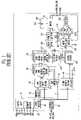
- FIG. 1is a functional block diagram illustrating the configuration of a DDR SDRAM in the prior art.
- a control logic 10includes a command decoder 20 and a mode register 30 .
- a clock enable signal CKEn, a clock signal CK, a clock bar signal /CK, a chip select signal /CSn, a write enable signal /WE, a column address strobe signal /CAS and a row address strobe signal /RASare input to the control logic 10 .
- block select addresses BA 0 , BA 1 and addresses A 0 to A 13are input to the control logic 10 through an address register 40 .
- the command decoder 20generates read, write and precharge commands, etc. according to an input signal.
- the mode register 30generates a CAS latency value and a burst length value according to an input address.
- a row address multiplexer 60generates a row address according to an input address and also generates the row address according to an address outputted from a refresh counter 50 .
- a bank row address latch and decoder 90outputs a bank select signal for selecting a memory bank, and is controlled by means of a bank control logic 70 .
- a column decoder 130generates a column address according to input addresses.
- a column address counter and latch 80generates a plurality of column addresses for a burst operation if an address is received, and provides the generated column addresses to the column decoder 130 .
- the column address counter and latch 80also generates a signal col 0 that divides even and odd regions of a memory bank.
- a bank memory array 100is composed of a plurality of memory banks. The memory banks are selected according to a bank select signal. Each of the memory banks consists of a plurality of cells, which are selected according to a row address and a column address.
- a I/O gating DM mask logic 120controls the input of data to the memory banks. Data write is controlled according to a data mask signal.
- the data of the memory banksare amplified in a sense amplifier 110 and then latched in a read latch 140 via the I/O gating DM mask logic 120 .
- the data latched in the read latch 140is transferred to a driver 170 according to the operation of a multiplexer 150 .
- the datais synchronized to DQS data from a DQS generator 180 and then outputted to an external chipset.
- the data from the external chipsetis input to a receiver 200 in synchronism with external DQS data.
- the data from the receiver 200is stored in an input register 210 and input to the write FIFO and driver 190 .
- the data from the write FIFO and driver 190is written into a corresponding cell through the I/O gating DM mask logic 120 and the sense amplifier 110 according to a mask signal. Meanwhile, a clock CLK is applied to the driver 170 through a delay lock loop (DLL) 160 .
- DLLdelay lock loop
- the DDR SDRAM constructed aboveneeds a column address counter because there exists a burst operation in the read and write operations.
- the column address counteroperates in accordance with a timing at which the sense amplifier reads or writes data. That is, in the read operation, the column address counter operates at a clock to which a read command is applied. In the write operation, it operates after 2*tCK since a write command is applied. This is because 1*tCK is needed to align internal data, as can be seen from FIG. 2 . In the DDR SDRAM, write data are applied later than the write command. It is also required that data latched at the rising edge of DQS be aligned at the falling edge of DQS, as shown in FIG. 2 .
- a data D 0is latched at a first rising edge of DQS, and the data D 0 is aligned while a data D 1 is latched at a first falling edge of DQS.
- a data D 2is latched at a second rising edge of DQS, and the data D 2 is aligned while a data D 3 is latched at a second falling edge of DQS.
- the present inventionhas been made in view of the above problems, and it is an object of the present invention to provide a semiconductor memory device in which the current consumed in a column address counter at the time of a read operation can be reduced.
- a semiconductor memory deviceincluding delay circuits for delaying a bank address and a column address in a write operation, comprising a controller for disabling the operation of the delay circuits in a read operation.
- FIG. 1is a functional block diagram illustrating the configuration of a DDR SDRAM in the prior art
- FIG. 2a write timing diagram of FIG. 1 ;
- FIG. 3is a block diagram illustrating some of a column address counter and a latch according to an embodiment of the present invention
- FIG. 4is a detailed circuit diagram of a delay unit shown in FIG. 3 ;
- FIG. 5is a timing diagram for explaining the operation of FIG. 3 ;
- FIG. 6is a block diagram of a column address counter and a latch according to another embodiment of the present invention.
- FIG. 7is a circuit diagram for explaining another embodiment of the present invention.
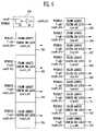
- FIG. 3is a schematic block diagram of a column address counter and a latch according to an embodiment of the present invention.
- a control signal casp6_rdis enabled, and a column address Y-add is thus provided to a counter 804 through a bypass unit 801 .
- a controller 802generates a control signal according to a signal casp 6 , which is enabled in the write and read operations, and a signal WT6RD5Z, which is enabled in the write operation and disabled in the read operation.
- the column address Y-addcan be provided to a delay unit 803 or block according to an output signal of the controller 802 .
- the delay unit 803delays the received column address Y-add by 2*tCK and provides the delayed column address to the counter 804 .
- the delay unit 803is not driven in the read operation but only in the write operation.
- FIG. 4is a detailed circuit diagram of the controller and the delay unit shown in FIG. 3 . The operation of each of the controller and the delay unit will now be described in detail with reference to FIG. 5 .
- the controller 802includes a NAND gate G 1 .
- the NAND gate G 1receives a signal CASP6, which is enabled according to a write command WRITE or a read command READ shown in FIG. 5 , and a signal WT6RD5Z, which is enabled according to the write command and disabled according to the read command, as inputs. If these two signals CASP6 and WT6RD5Z are at a logic HIGH state, the output of the NAND gate G 1 becomes a logic LOW state. If the output of the NAND gate G 1 becomes a logic LOW state, the output of an inverter G 2 becomes a logic HIGH state, and a transfer gate T 1 is thus turned on.
- a received column addressis provided to a latch L 1 through the transfer gate T 1 .
- transfer gates T 2 to T 5are turned according to a signal clkp 4 , which is enabled at the rising edge of a clock CLK and a signal inverted by an inverter G 3 .
- the column address through the transfer gate T 1is output to an output terminal out via latches L 1 to L 5 and an inverter G 4 . That is, the delay unit 803 delays an input column address as much as 2*tck only in the write operation, but does not perform a shifting operation in the read operation. As a result, it is possible to reduce current consumption that much.
- a memory devicesuch as a DDR DRAM is composed of a plurality of column address counter and latches. At this time, the controller constructed above can be installed in each block.
- FIG. 6is a block diagram of column address counter and latches according to another embodiment of the present invention.
- the controlleris additionally installed every column address counter and latch. In the embodiment of FIG. 6 , however, one controller is used to control the 13 column address counter and latch blocks.
- 13 column address counters and latches 901 to 913are controlled according to outputs casp6_dly of a controller 914 .
- the controller 914consists of a NAND gate G 5 and an inverter G 6 , and receives the signal CASP6, which is enabled according to the write command WRITE or the read command READ shown in FIG. 5 , and the signal WT6RD5Z, which is enabled according to the write command and disabled according to the read command, as inputs. If both the signals CASP6 and WT6RD5Z are at a logic HIGH state, the output of the NAND gate G 5 becomes a logic LOW state.
- the output casp_dly of the inverter G 6becomes a logic HIGH state.
- the output casp_dly of the inverter G 6is provided to the column address counter and latches 901 to 903 . Accordingly, a shifting operation of a delay unit, which is included in each of the column address counter and latches 901 to 903 and delays the column address as much as 2*tck in the read operation is blocked. It is thus possible to reduce current consumption to that extent.
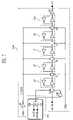
- FIG. 7is a circuit diagram for explaining another embodiment of the present invention.
- a controller 915is composed of a NAND gate G 7 , and receives the signal CASP 6 , which is enabled according to the write command WRITE or the read command READ shown in FIG. 5 , and the signal WT6RD5Z, which is enabled according to the write command and disabled according to the read command, as inputs. If both the signals CASP6 and WT6RD5Z are at a logic HIGH state, the output of the NAND gate G 7 becomes a logic LOW state. If the output of the NAND gate G 7 becomes a logic LOW state, the output of an inverter G 10 becomes a logic HIGH state, and a transfer gate T 6 is thus turned on.
- transfer gates T 7 to T 10are turned on according to the signal clkp4, which is enabled at the rising edge of the clock CLK and a signal clkpl4z inverted by an inverter G 8 .
- a latched bank address eat_bkis delayed through the transfer gates T 6 to T 10 and latches L 6 to L 10 and outputs to an output terminal out via an inverter G 11 . That is, a delay unit 1000 delays an inputted bank address as much as 2*tck only in the write operation, but does not perform a shift operation in the read operation. Accordingly, current consumption can be saved.
- a 256 Mb DDR SDRAMneeds four circuits as shown in FIG. 7 since it is 4 banks. Accordingly, if the shift operation of these circuits is blocked in the read operation, current consumption can be saved to that extent.
- the present inventionis advantageous in a low-power operation of a DDR SDRAM.
Landscapes
- Engineering & Computer Science (AREA)
- Microelectronics & Electronic Packaging (AREA)
- Computer Hardware Design (AREA)
- Databases & Information Systems (AREA)
- Dram (AREA)
- Static Random-Access Memory (AREA)
Abstract
Description
Claims (19)
Applications Claiming Priority (2)
| Application Number | Priority Date | Filing Date | Title |
|---|---|---|---|
| KR10-2004-90254 | 2004-11-08 | ||
| KR1020040090254AKR100624296B1 (en) | 2004-11-08 | 2004-11-08 | Semiconductor memory device |
Publications (2)
| Publication Number | Publication Date |
|---|---|
| US20060098502A1 US20060098502A1 (en) | 2006-05-11 |
| US7248512B2true US7248512B2 (en) | 2007-07-24 |
Family
ID=36316158
Family Applications (1)
| Application Number | Title | Priority Date | Filing Date |
|---|---|---|---|
| US11/157,834Expired - Fee RelatedUS7248512B2 (en) | 2004-11-08 | 2005-06-22 | Semiconductor memory device having controller with improved current consumption |
Country Status (5)
| Country | Link |
|---|---|
| US (1) | US7248512B2 (en) |
| JP (1) | JP5144882B2 (en) |
| KR (1) | KR100624296B1 (en) |
| CN (1) | CN1790544B (en) |
| TW (1) | TWI289860B (en) |
Cited By (21)
| Publication number | Priority date | Publication date | Assignee | Title |
|---|---|---|---|---|
| US20070070730A1 (en)* | 2005-09-29 | 2007-03-29 | Hynix Semiconductor Inc. | Semiconductor memory device |
| US20090168567A1 (en)* | 2007-12-26 | 2009-07-02 | Hynix Semiconductor, Inc. | Semiconductor memory device |
| US20100329050A1 (en)* | 2007-03-22 | 2010-12-30 | Kyung-Whan Kim | Semiconductor memory device |
| US20120020171A1 (en)* | 2010-07-21 | 2012-01-26 | International Business Machines Corporation | Memory system with delay locked loop (dll) bypass control |
| US8913448B2 (en)* | 2012-10-25 | 2014-12-16 | Micron Technology, Inc. | Apparatuses and methods for capturing data in a memory |
| US8984320B2 (en) | 2011-03-29 | 2015-03-17 | Micron Technology, Inc. | Command paths, apparatuses and methods for providing a command to a data block |
| US8988966B2 (en) | 2007-03-15 | 2015-03-24 | Micron Technology, Inc. | Circuit, system and method for controlling read latency |
| US9001594B2 (en) | 2012-07-06 | 2015-04-07 | Micron Technology, Inc. | Apparatuses and methods for adjusting a path delay of a command path |
| US9000817B2 (en) | 2012-02-01 | 2015-04-07 | Micron Technology, Inc. | Apparatuses and methods for altering a forward path delay of a signal path |
| US9054675B2 (en) | 2012-06-22 | 2015-06-09 | Micron Technology, Inc. | Apparatuses and methods for adjusting a minimum forward path delay of a signal path |
| US9166579B2 (en) | 2012-06-01 | 2015-10-20 | Micron Technology, Inc. | Methods and apparatuses for shifting data signals to match command signal delay |
| US9329623B2 (en) | 2012-08-22 | 2016-05-03 | Micron Technology, Inc. | Apparatuses, integrated circuits, and methods for synchronizing data signals with a command signal |
| US9508417B2 (en) | 2014-02-20 | 2016-11-29 | Micron Technology, Inc. | Methods and apparatuses for controlling timing paths and latency based on a loop delay |
| US9530473B2 (en) | 2014-05-22 | 2016-12-27 | Micron Technology, Inc. | Apparatuses and methods for timing provision of a command to input circuitry |
| US9529379B2 (en) | 2006-12-19 | 2016-12-27 | Micron Technology, Inc. | Timing synchronization circuit with loop counter |
| US9531363B2 (en) | 2015-04-28 | 2016-12-27 | Micron Technology, Inc. | Methods and apparatuses including command latency control circuit |
| US9601170B1 (en) | 2016-04-26 | 2017-03-21 | Micron Technology, Inc. | Apparatuses and methods for adjusting a delay of a command signal path |
| US9813067B2 (en) | 2015-06-10 | 2017-11-07 | Micron Technology, Inc. | Clock signal and supply voltage variation tracking |
| US9865317B2 (en) | 2016-04-26 | 2018-01-09 | Micron Technology, Inc. | Methods and apparatuses including command delay adjustment circuit |
| US9997220B2 (en) | 2016-08-22 | 2018-06-12 | Micron Technology, Inc. | Apparatuses and methods for adjusting delay of command signal path |
| US10224938B2 (en) | 2017-07-26 | 2019-03-05 | Micron Technology, Inc. | Apparatuses and methods for indirectly detecting phase variations |
Families Citing this family (4)
| Publication number | Priority date | Publication date | Assignee | Title |
|---|---|---|---|---|
| KR100893577B1 (en)* | 2007-06-26 | 2009-04-17 | 주식회사 하이닉스반도체 | Semiconductor memory device |
| CN105720954A (en)* | 2016-03-17 | 2016-06-29 | 成都集思科技有限公司 | Temperature compensation delay line |
| CN106128500B (en)* | 2016-07-25 | 2023-02-24 | 西安紫光国芯半导体有限公司 | Fast decoder and decoding method for dynamic random access memory |
| KR102638793B1 (en)* | 2018-10-01 | 2024-02-21 | 에스케이하이닉스 주식회사 | Semiconductor device |
Citations (12)
| Publication number | Priority date | Publication date | Assignee | Title |
|---|---|---|---|---|
| US5493241A (en)* | 1994-11-16 | 1996-02-20 | Cypress Semiconductor, Inc. | Memory having a decoder with improved address hold time |
| US5568445A (en) | 1994-03-03 | 1996-10-22 | Samsung Electronics Co., Ltd. | Synchronous semiconductor memory device with a write latency control function |
| JPH09171681A (en) | 1995-12-21 | 1997-06-30 | Nec Ic Microcomput Syst Ltd | Memory address controller |
| US5691955A (en) | 1995-09-05 | 1997-11-25 | Mitsubishi Denki Kabushiki Kaisha | Synchronous semiconductor memory device operating in synchronization with external clock signal |
| JPH10106288A (en) | 1997-11-07 | 1998-04-24 | Matsushita Electric Ind Co Ltd | Semiconductor storage device |
| JPH10275467A (en) | 1997-04-01 | 1998-10-13 | Hitachi Ltd | Semiconductor storage device and data processing device |
| JPH1196760A (en) | 1997-09-24 | 1999-04-09 | Fujitsu Ltd | Semiconductor storage device |
| US5966724A (en) | 1996-01-11 | 1999-10-12 | Micron Technology, Inc. | Synchronous memory device with dual page and burst mode operations |
| US6343040B2 (en)* | 2000-02-24 | 2002-01-29 | Samsung Electronics Co., Ltd. | Auto precharge control signal generating circuits for semiconductor memory devices and auto precharge control methods |
| US6356507B1 (en)* | 1999-09-22 | 2002-03-12 | Kabushiki Kaisha Toshiba | Synchronous DRAM using column operation sychronous pulses which are different between read and write |
| US20030179613A1 (en)* | 2002-03-20 | 2003-09-25 | Mitsubishi Denki Kabushiki Kaisha | Semiconductor device outputting data at a timing with reduced jitter |
| US20050232044A1 (en)* | 2004-04-02 | 2005-10-20 | Hitachi, Ltd. | Semiconductor memory device |
Family Cites Families (9)
| Publication number | Priority date | Publication date | Assignee | Title |
|---|---|---|---|---|
| JPS60253315A (en)* | 1984-05-30 | 1985-12-14 | Nec Corp | Variable delay circuit |
| JPS6135011A (en)* | 1984-07-26 | 1986-02-19 | Nec Corp | Variable delay circuit |
| CN1137845A (en)* | 1994-09-15 | 1996-12-11 | 菲利浦电子有限公司 | Delay unit transmission system using such delay unit |
| JPH1064257A (en)* | 1996-08-20 | 1998-03-06 | Sony Corp | Semiconductor storage |
| JP3695902B2 (en)* | 1997-06-24 | 2005-09-14 | 富士通株式会社 | Semiconductor memory device |
| JP3270831B2 (en)* | 1998-02-03 | 2002-04-02 | 富士通株式会社 | Semiconductor device |
| JP4216415B2 (en)* | 1999-08-31 | 2009-01-28 | 株式会社ルネサステクノロジ | Semiconductor device |
| JP4345204B2 (en)* | 2000-07-04 | 2009-10-14 | エルピーダメモリ株式会社 | Semiconductor memory device |
| JP2002184864A (en)* | 2000-10-03 | 2002-06-28 | Mitsubishi Electric Corp | Semiconductor device |
- 2004
- 2004-11-08KRKR1020040090254Apatent/KR100624296B1/ennot_activeExpired - Fee Related
- 2005
- 2005-06-13TWTW094119504Apatent/TWI289860B/ennot_activeIP Right Cessation
- 2005-06-22USUS11/157,834patent/US7248512B2/ennot_activeExpired - Fee Related
- 2005-08-12JPJP2005234805Apatent/JP5144882B2/ennot_activeExpired - Fee Related
- 2005-11-07CNCN2005101202425Apatent/CN1790544B/ennot_activeExpired - Fee Related
Patent Citations (12)
| Publication number | Priority date | Publication date | Assignee | Title |
|---|---|---|---|---|
| US5568445A (en) | 1994-03-03 | 1996-10-22 | Samsung Electronics Co., Ltd. | Synchronous semiconductor memory device with a write latency control function |
| US5493241A (en)* | 1994-11-16 | 1996-02-20 | Cypress Semiconductor, Inc. | Memory having a decoder with improved address hold time |
| US5691955A (en) | 1995-09-05 | 1997-11-25 | Mitsubishi Denki Kabushiki Kaisha | Synchronous semiconductor memory device operating in synchronization with external clock signal |
| JPH09171681A (en) | 1995-12-21 | 1997-06-30 | Nec Ic Microcomput Syst Ltd | Memory address controller |
| US5966724A (en) | 1996-01-11 | 1999-10-12 | Micron Technology, Inc. | Synchronous memory device with dual page and burst mode operations |
| JPH10275467A (en) | 1997-04-01 | 1998-10-13 | Hitachi Ltd | Semiconductor storage device and data processing device |
| JPH1196760A (en) | 1997-09-24 | 1999-04-09 | Fujitsu Ltd | Semiconductor storage device |
| JPH10106288A (en) | 1997-11-07 | 1998-04-24 | Matsushita Electric Ind Co Ltd | Semiconductor storage device |
| US6356507B1 (en)* | 1999-09-22 | 2002-03-12 | Kabushiki Kaisha Toshiba | Synchronous DRAM using column operation sychronous pulses which are different between read and write |
| US6343040B2 (en)* | 2000-02-24 | 2002-01-29 | Samsung Electronics Co., Ltd. | Auto precharge control signal generating circuits for semiconductor memory devices and auto precharge control methods |
| US20030179613A1 (en)* | 2002-03-20 | 2003-09-25 | Mitsubishi Denki Kabushiki Kaisha | Semiconductor device outputting data at a timing with reduced jitter |
| US20050232044A1 (en)* | 2004-04-02 | 2005-10-20 | Hitachi, Ltd. | Semiconductor memory device |
Cited By (35)
| Publication number | Priority date | Publication date | Assignee | Title |
|---|---|---|---|---|
| US20070070730A1 (en)* | 2005-09-29 | 2007-03-29 | Hynix Semiconductor Inc. | Semiconductor memory device |
| US20090052271A1 (en)* | 2005-09-29 | 2009-02-26 | Hynix Semiconductor Inc. | Semiconductor memory device |
| US7529140B2 (en)* | 2005-09-29 | 2009-05-05 | Hynix Semiconductor Inc. | Semiconductor memory device |
| US7675810B2 (en) | 2005-09-29 | 2010-03-09 | Hynix Semiconductor, Inc. | Semiconductor memory device |
| US9529379B2 (en) | 2006-12-19 | 2016-12-27 | Micron Technology, Inc. | Timing synchronization circuit with loop counter |
| US10658019B2 (en) | 2007-03-15 | 2020-05-19 | Micron Technology, Inc. | Circuit, system and method for controlling read latency |
| US8988966B2 (en) | 2007-03-15 | 2015-03-24 | Micron Technology, Inc. | Circuit, system and method for controlling read latency |
| US20100329050A1 (en)* | 2007-03-22 | 2010-12-30 | Kyung-Whan Kim | Semiconductor memory device |
| US8050118B2 (en)* | 2007-03-22 | 2011-11-01 | Hynix Semiconductor Inc. | Semiconductor memory device |
| US20120044773A1 (en)* | 2007-03-22 | 2012-02-23 | Kyung-Whan Kim | Semiconductor memory device |
| US8320197B2 (en)* | 2007-03-22 | 2012-11-27 | Hynix Semiconductor Inc. | Semiconductor memory device |
| US7835204B2 (en)* | 2007-12-26 | 2010-11-16 | Hynix Semiconductor Inc. | Semiconductor memory device for generating column address |
| US20090168567A1 (en)* | 2007-12-26 | 2009-07-02 | Hynix Semiconductor, Inc. | Semiconductor memory device |
| US20120020171A1 (en)* | 2010-07-21 | 2012-01-26 | International Business Machines Corporation | Memory system with delay locked loop (dll) bypass control |
| US8379459B2 (en)* | 2010-07-21 | 2013-02-19 | International Business Machines Corporation | Memory system with delay locked loop (DLL) bypass control |
| US8984320B2 (en) | 2011-03-29 | 2015-03-17 | Micron Technology, Inc. | Command paths, apparatuses and methods for providing a command to a data block |
| US9000817B2 (en) | 2012-02-01 | 2015-04-07 | Micron Technology, Inc. | Apparatuses and methods for altering a forward path delay of a signal path |
| US9166579B2 (en) | 2012-06-01 | 2015-10-20 | Micron Technology, Inc. | Methods and apparatuses for shifting data signals to match command signal delay |
| US9054675B2 (en) | 2012-06-22 | 2015-06-09 | Micron Technology, Inc. | Apparatuses and methods for adjusting a minimum forward path delay of a signal path |
| US9001594B2 (en) | 2012-07-06 | 2015-04-07 | Micron Technology, Inc. | Apparatuses and methods for adjusting a path delay of a command path |
| US9329623B2 (en) | 2012-08-22 | 2016-05-03 | Micron Technology, Inc. | Apparatuses, integrated circuits, and methods for synchronizing data signals with a command signal |
| US8913448B2 (en)* | 2012-10-25 | 2014-12-16 | Micron Technology, Inc. | Apparatuses and methods for capturing data in a memory |
| US9508417B2 (en) | 2014-02-20 | 2016-11-29 | Micron Technology, Inc. | Methods and apparatuses for controlling timing paths and latency based on a loop delay |
| US9530473B2 (en) | 2014-05-22 | 2016-12-27 | Micron Technology, Inc. | Apparatuses and methods for timing provision of a command to input circuitry |
| US9531363B2 (en) | 2015-04-28 | 2016-12-27 | Micron Technology, Inc. | Methods and apparatuses including command latency control circuit |
| US9813067B2 (en) | 2015-06-10 | 2017-11-07 | Micron Technology, Inc. | Clock signal and supply voltage variation tracking |
| US10193558B2 (en) | 2015-06-10 | 2019-01-29 | Micron Technology, Inc. | Clock signal and supply voltage variation tracking |
| US9865317B2 (en) | 2016-04-26 | 2018-01-09 | Micron Technology, Inc. | Methods and apparatuses including command delay adjustment circuit |
| US10290336B2 (en) | 2016-04-26 | 2019-05-14 | Micron Technology, Inc. | Methods and apparatuses including command delay adjustment circuit |
| US9601170B1 (en) | 2016-04-26 | 2017-03-21 | Micron Technology, Inc. | Apparatuses and methods for adjusting a delay of a command signal path |
| US10755758B2 (en) | 2016-04-26 | 2020-08-25 | Micron Technology, Inc. | Methods and apparatuses including command delay adjustment circuit |
| US9997220B2 (en) | 2016-08-22 | 2018-06-12 | Micron Technology, Inc. | Apparatuses and methods for adjusting delay of command signal path |
| US11087806B2 (en) | 2016-08-22 | 2021-08-10 | Micron Technology, Inc. | Apparatuses and methods for adjusting delay of command signal path |
| US10224938B2 (en) | 2017-07-26 | 2019-03-05 | Micron Technology, Inc. | Apparatuses and methods for indirectly detecting phase variations |
| US10797708B2 (en) | 2017-07-26 | 2020-10-06 | Micron Technology, Inc. | Apparatuses and methods for indirectly detecting phase variations |
Also Published As
| Publication number | Publication date |
|---|---|
| US20060098502A1 (en) | 2006-05-11 |
| CN1790544A (en) | 2006-06-21 |
| TW200615977A (en) | 2006-05-16 |
| KR100624296B1 (en) | 2006-09-19 |
| TWI289860B (en) | 2007-11-11 |
| JP5144882B2 (en) | 2013-02-13 |
| JP2006134554A (en) | 2006-05-25 |
| CN1790544B (en) | 2011-06-15 |
| KR20060040965A (en) | 2006-05-11 |
Similar Documents
| Publication | Publication Date | Title |
|---|---|---|
| US7248512B2 (en) | Semiconductor memory device having controller with improved current consumption | |
| US10872646B2 (en) | Apparatuses and methods for providing active and inactive clock signals | |
| US8154933B2 (en) | Mode-register reading controller and semiconductor memory device | |
| US7751261B2 (en) | Method and apparatus for controlling read latency of high-speed DRAM | |
| US10860469B2 (en) | Apparatuses and methods for providing internal memory commands and control signals in semiconductor memories | |
| US6424590B1 (en) | Semiconductor device | |
| US8625364B2 (en) | Semiconductor memory devices and systems including data output circuits to output stored data during first output mode and output programmed data pattern during second output mode | |
| US20130250705A1 (en) | Clock signal generation apparatus for use in semiconductor memory device and its method | |
| US20070011483A1 (en) | Delay-lock loop and method adapting itself to operate over a wide frequency range | |
| US20100085824A1 (en) | Semiconductor device having delay control circuit | |
| US8406080B2 (en) | Data output control circuit of a double data rate (DDR) synchronous semiconductor memory device responsive to a delay locked loop (DLL) clock and method thereof | |
| US7515482B2 (en) | Pipe latch device of semiconductor memory device | |
| CN101026006A (en) | Latency control circuit and method thereof and an auto-precharge control circuit and method thereof | |
| US11848070B2 (en) | Memory with DQS pulse control circuitry, and associated systems, devices, and methods | |
| US12367133B2 (en) | Apparatuses and methods for training operations | |
| US11417388B2 (en) | Processing of unassigned row address in a memory |
Legal Events
| Date | Code | Title | Description |
|---|---|---|---|
| AS | Assignment | Owner name:HYNIX SEMICONDUCTOR INC., KOREA, REPUBLIC OF Free format text:ASSIGNMENT OF ASSIGNORS INTEREST;ASSIGNOR:SHIN, BEOM JU;REEL/FRAME:016720/0010 Effective date:20050228 | |
| STCF | Information on status: patent grant | Free format text:PATENTED CASE | |
| FEPP | Fee payment procedure | Free format text:PAYOR NUMBER ASSIGNED (ORIGINAL EVENT CODE: ASPN); ENTITY STATUS OF PATENT OWNER: LARGE ENTITY | |
| FEPP | Fee payment procedure | Free format text:PAYER NUMBER DE-ASSIGNED (ORIGINAL EVENT CODE: RMPN); ENTITY STATUS OF PATENT OWNER: LARGE ENTITY Free format text:PAYOR NUMBER ASSIGNED (ORIGINAL EVENT CODE: ASPN); ENTITY STATUS OF PATENT OWNER: LARGE ENTITY | |
| FPAY | Fee payment | Year of fee payment:4 | |
| FPAY | Fee payment | Year of fee payment:8 | |
| FEPP | Fee payment procedure | Free format text:MAINTENANCE FEE REMINDER MAILED (ORIGINAL EVENT CODE: REM.); ENTITY STATUS OF PATENT OWNER: LARGE ENTITY | |
| LAPS | Lapse for failure to pay maintenance fees | Free format text:PATENT EXPIRED FOR FAILURE TO PAY MAINTENANCE FEES (ORIGINAL EVENT CODE: EXP.); ENTITY STATUS OF PATENT OWNER: LARGE ENTITY | |
| STCH | Information on status: patent discontinuation | Free format text:PATENT EXPIRED DUE TO NONPAYMENT OF MAINTENANCE FEES UNDER 37 CFR 1.362 | |
| FP | Lapsed due to failure to pay maintenance fee | Effective date:20190724 |