US7248345B2 - Signal processing method for use with an optical navigation system - Google Patents
Signal processing method for use with an optical navigation systemDownload PDFInfo
- Publication number
- US7248345B2 US7248345B2US11/268,898US26889805AUS7248345B2US 7248345 B2US7248345 B2US 7248345B2US 26889805 AUS26889805 AUS 26889805AUS 7248345 B2US7248345 B2US 7248345B2
- Authority
- US
- United States
- Prior art keywords
- phase
- phase signals
- signals
- signal
- array
- Prior art date
- Legal status (The legal status is an assumption and is not a legal conclusion. Google has not performed a legal analysis and makes no representation as to the accuracy of the status listed.)
- Active, expires
Links
Images


Classifications
- G—PHYSICS
- G06—COMPUTING OR CALCULATING; COUNTING
- G06F—ELECTRIC DIGITAL DATA PROCESSING
- G06F3/00—Input arrangements for transferring data to be processed into a form capable of being handled by the computer; Output arrangements for transferring data from processing unit to output unit, e.g. interface arrangements
- G06F3/01—Input arrangements or combined input and output arrangements for interaction between user and computer
- G06F3/03—Arrangements for converting the position or the displacement of a member into a coded form
- G06F3/0304—Detection arrangements using opto-electronic means
- G06F3/0317—Detection arrangements using opto-electronic means in co-operation with a patterned surface, e.g. absolute position or relative movement detection for an optical mouse or pen positioned with respect to a coded surface
Definitions
- the present inventionrelates generally to signal processing, and more particularly to a signal processing circuit and method for use with an optical navigation system for determining movement of an optical sensor relative to a surface without the use of sinusoidal signals.
- Signal processorsare used in a wide range of applications including, for example, measuring a current output from a photo-detector of an array in an optical navigation system.
- Optical navigation systemssuch as an optical computer mouse or trackball, are well known for inputting data into and interfacing with personal computers and workstations. Such devices allow rapid relocation of a cursor on a monitor, and are useful in many text, database and graphical programs.
- a usercontrols the cursor, for example, by moving the mouse over a surface to move the cursor in a direction and over distance proportional to the movement of the mouse. Alternatively, movement of the hand over a stationary device may be used for the same purpose.
- the dominant technology used today for optical micerelies on a light source illuminating a surface, a two-dimensional (2D) array of photosensitive elements to capture the resultant images, and a signal processor that correlates successive images to detect and quantify the motion of the mouse.
- the imagecan be produced in a number of ways including illuminating the surface at or near grazing incidence to produce and image shadows due to roughness of the surface, illumination with a coherent light source to produce a speckle image of the surface, or the use of a pattern printed onto the surface itself.
- a processorcaptures the image and does a series of correlations between successive images to determine the most likely motion between frames.
- a similar methodcan be used with a linear sensor to track one dimension (1D) motion.
- the correlation used to track the motion of the imagerequires a great deal of processing and results in an unsatisfactory power consumption that limits the usefulness of the technique in power sensitive applications, such as wireless mice.
- An alternative method to correlationuses a linear or 1D array of photosensitive elements or detectors, such as photodiodes, in which the output of the individual elements in the array are combined or wired together in a repeating pattern spanning two or more detectors to track motion along one axis or in one dimension.
- the detectorsare wired together in a pattern spanning from about four (4) to about (10) elements, a number referred to here as the M value of the array. This results in M discrete outputs from the array.
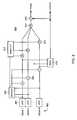
- An example of such an array with an M value of 4is shown in FIG. 1 .
- the arrayshown is a 1D comb-array 102 of photosensitive elements 104 directly wired in groups to detect of motion through movement of a light-dark pattern known as speckle.
- Speckleis the complex interference pattern generated by scattering of coherent light off of an optically rough surface and detected by a photosensitive element, such as a photodiode, with a finite angular field-of-view or numerical aperture.
- the image mapped to or captured on the 1D comb-arraymay be magnified or de-magnified to achieve matching and so that the distribution of spatial frequencies in the image is roughly centered around the spatial frequencies of the array.
- a signal processor or signal processing circuit and methodthat is capable of tracking motion from an optical sensor without requiring the generation and processing of quasi-sinusoidal signals for tracking, thereby providing motion tracking from a single processing path with much simpler signal processing requirements. It is desirable that the signal processing circuit and method are capable of tracking motion from a comb-array having an arbitrary M value. It is still further desirable that the circuit and method can be applied to both speckle and non-speckle based devices, and to devices or optical sensors having either 1D or 2D arrays.
- FIG. 1(prior art) is a schematic block diagram of a linear, one-dimensional (1D) comb-array having a number of photodiodes in which every fourth photosensitive element is coupled together to provide an M value of 4;
- FIG. 2is a functional block diagram of an optical navigation system having a signal processing circuit for processing signals according to an embodiment of the method of the present invention
- FIG. 3is a schematic block diagram of a linear, 1D comb-array having an M value of 5 for which a signal processing method according to the present invention is useful;
- FIG. 4is a flowchart of a signal processing method according to an embodiment of the present invention.
- FIG. 6is a block diagram of a signal processing circuit according to an embodiment of the present invention.
- FIGS. 7 through 10are schematic block diagrams of various embodiments of sensor arrays having multiple one-dimensional 1D arrays arranged along multiple axes for which a signal processing circuit and method according to the present invention are particularly useful;
- FIGS. 11A and 11Bare schematic block diagrams of a two-dimensional comb-array for which a signal processing circuit and method according to the present invention are particularly useful.
- FIGS. 12A through 12Dare schematic block diagrams of various embodiments for grouping photosensitive elements in a two-dimensional comb-array according to the present invention.
- the present inventionis directed to signal processors or signal processing circuits and methods, and more particularly for use in optical navigation systems with comb detector arrays to determine motion of the system relative to a surface without the use of sinusoidal signals.
- Optical navigation systemscan include, for example, an optical computer mouse, trackballs and the like, and are well known for inputting data into and interfacing with personal computers and workstations.
- optical navigation systemscan include, for example, an optical computer mouse, trackballs and the like, and are well known for inputting data into and interfacing with personal computers and workstations.
- many of the details of optical navigation systems in general and optical sensors for optical navigation systems in particular that are widely known and are not relevant to the present inventionhave been omitted from the following description.
- Optical navigation systems and optical sensorsare described, for example, in co-pending, commonly assigned U.S. patent application Ser. No. 11/129,967, entitled, “Optical Positioning Device Having Shaped Illumination,” filed on May 16, 2005 by Clinton B. Carlisle et al., and incorporated herein by reference in its entirety.
- the signal processing circuits and method of the present inventioninvolves detecting and measuring changes in phase of a strong spatial frequency of a signal captured by an optical sensor as it is moved relative to a surface over which it is positioned. Information on the magnitude and direction of displacement of the sensor relative to the surface may then be determined using any of a number of signal processing methods to process the phase change information.
- the strong spatial frequency of a signalmatches a period of the sensor.
- the optical sensoris a speckle-based sensor, which senses movement based on displacement of a complex intensity distribution pattern of light, known as speckle.
- Speckleis essentially the complex interference pattern generated by scattering of coherent light off of a rough surface and detected by a photosensitive element, such as a photodiode, with a finite angular field-of-view (or numerical aperture).
- a photosensitive elementsuch as a photodiode
- a finite angular field-of-viewor numerical aperture.
- the method and circuit of the present inventionis not limited to speckle-based sensors, and can be used with other types of illumination, including coherent and non-coherent light sources, and images having the signal captured by the optical sensor with a strong spatial frequency matching a period of the sensor.
- an optical navigation system 200generally includes an optical head 202 having an illuminator 204 with a light source 206 and illumination optics 208 to illuminate a portion of a surface 210 , imaging optics 212 to map or image a pattern of the by the surface, and an optical sensor 214 to sense or detect change in the pattern.
- the optical sensor 214includes one or more one-dimensional (1D) or two-dimensional (2D) arrays 216 each having a number of photosensitive elements, such as photodiodes 218 , on which light reflected from the surface 210 is received.
- the array(s) 216may be configured to provide displacement measurements along two orthogonal axes, x and y.
- the optical navigation system 200further includes signal processing circuitry 222 for processing signals from the array(s) 216 in accordance with the method of the present invention. Groups of photodiodes 218 in the array(s) 216 may be combined or wire summed to produce group signals. These group signals are subsequently processed by the signal processing circuitry 222 using an algorithm 226 to produce ⁇ x, ⁇ y data 228 providing information on the magnitude and direction of displacement of the optical head 202 in x and y directions.
- FIG. 3shows a general configuration (along one axis) of a 1D comb-array 302 of photosensitive elements, such as photodiodes 304 , wherein the combination of interlaced groups of photosensitive elements serves as a periodic filter on spatial frequencies of light-dark signals 306 produced by the speckle (or non-speckle) images mapped to the array.
- the 1D comb-array 302consists of a number of photodiode sets or periods 308 , each having five of photodiodes 304 , labeled here as A, B, C, D, and E.
- the width of the photodiode sets or periods 308is matched to the average period of the light-dark signals 306 to filter a desired signal arising from light originating with the light source and reflected from the surface.
- an average diameter of the speckle or light-dark pattern mapped or imaged to the 1D comb-array 302is corresponds to the photodiodes 304 width such that the diameter of one light and one dark spot is substantially equal to the M value of the array, or the sum of the widths of photodiodes in a period 308 .
- the 1D comb-array 302is one of multiple 1D comb-arrays in an optical sensor in which two or more 1D arrays are arranged along non-parallel axes to measure two-dimensional displacement.
- Exemplary embodiments of various sensor arrays having multiple one-dimensional 1D arrays arranged along multiple axes to measure two-dimensional displacementare shown in FIGS. 6 through 9 , and described in greater detail below.
- the methodbegins with sampling each of a number (M) of phase signals from the plurality of photosensitive elements (step 402 ).
- Ma number of phase signals from the plurality of photosensitive elements
- Each of the M signalshas a magnitude (A i ) and includes a tracking signal at a frequency being tracked and a background signal at other frequencies that offsets the tracking signal, where i, an index of the signals, is a whole number between 0 and M-1.
- the offset to the tracking signal due to the background signalis eliminated to generate M non-offset phase signals having a magnitude (A′ i ) (step 404 ).
- phase angles ( ⁇ i ) of the non-offset phase signalsare then adjusted to generate M weighted phase signals (A′ i ⁇ ′ i ) (step 406 ).
- each of the M weighted phase signals (A′ i ⁇ ′ i )are combined to generate an average weighted phase having a phase angle ( ⁇ ) (step 408 ).
- the average weighted phase signalindicates a direction and velocity of the movement of an image of the surface mapped to the array.
- FIG. 3is a schematic block diagram of a linear, 1D comb-array having an M value of 5, and for which a signal processing method according to the present invention is useful.
- FIG. 5is a vector diagram or phase plot representing the signal strength of a number of signals from a 1D comb-array having an M value of 5.
- the outputs of the comb-array 302 shown in FIG. 3can be seen as representing the strength of the signal in each of M phases (A i ).
- Each of these M phasesis evenly distributed around a phase plot at an angle of ⁇ i .
- a mathematical expression of this distributionis shown in Eq. 1.0, where i is the index and angle ⁇ represents an arbitrary angular offset indicating that the exact alignment of each of the phases is unimportant, only that they are evenly distributed.
- phase angles described aboveproduce a large discontinuity between ⁇ 0 and ⁇ M as the value wraps.
- This discontinuityleads to difficulties in calculating the phase of the current signal.
- a minis A 0
- a minis at: ⁇ 0 ⁇ 1 ⁇ 2 ⁇ 3 ⁇ 4 A 0 0 72 144 216 288 A 1 0 72 ⁇ 216 ⁇ 144 ⁇ 72 A 2 0 72 144 ⁇ 144 ⁇ 72 A 3 0 72 144 216 ⁇ 72 A 4 0 72 144 216 288
- the weighted average of the phases, ⁇results in a phase angle that, when tracked over time, indicates the direction and velocity of the movement of the surface image across the optical sensor or array. (Note that the value of ⁇ Amin makes no contribution as A′ min will always be 0.)
- the largest magnitude signalis determined and subtracted to eliminate the offset caused by the background signal.
- the resulting difference in the calculated phaseis 1 ⁇ 2 of the rotation or 180° different from that calculated with the minimum signal. This has no effect on the ability to track motion.
- the calculated phase from the maximum and the minimumshould have a difference of 1 ⁇ 2 rotation when reliable signals are present. If the difference varies from 1 ⁇ 2 rotation, it is an indicator that one or more of the signals may be problematic. One example would be a situation where noise results in two minima or two maxima.
- phaseis calculated based on both the maximum and minimum, adjust one by 1 ⁇ 2 rotation, and the resulting phases averaged, thereby providing improved tracking performance.
- the signalsfor example A 0 to A 4 above, can also be used to measure the contrast of the image seen by the optical sensor or array. This is accomplished by summing of the signals as shown in equation 4.0 below.
- the resulting measurement, Cserves two important functions.
- the phase measurementmay become unreliable.
- the contrast of a speckle signalis usually closely related to the laser power directed at the surface being imaged.
- the contrast measurementconcentrates on the signal of interest and excludes other signals and ambient light, it can be used to drive an automatic gain control circuit to control the power output of the laser source.
- a very high contrastindicates that the laser power can be reduced while still maintaining acceptable tracking.
- a low contrastindicates that power output should be increased to maintain tracking.
- FIG. 5An embodiment of a signal processing circuit 600 for executing the above method is illustrated in FIG. 5 in a block diagram form.
- a number of line or group phase signals 602(shown here as signals 1 through M) from a sensor array (not shown) are converted from analog to digital values in multiple analog to digital converters (ADC) 604 .
- a minimum phase signalis determined or identified from among the number of phase signals 602 using a minimum detection circuitry 606 , and the identified minimum phase signal is subtracted from the remaining phase signals in multiple subtractors 608 .
- the resultant post subtraction phase signalsare multiplied in multipliers 610 by a predetermined angle value ( ⁇ i ) supplied from an angle look-up-table (LUT) 612 , such as that shown in Table I above, to generate post subtraction weighted phase signals.
- ⁇ ia predetermined angle value supplied from an angle look-up-table (LUT) 612 , such as that shown in Table I above.
- These weighted phase signalsare summed in an adder or summer 614 and divided in a divider 616 by a sum of the post subtraction unweighted phase signals supplied from adder 618 to provide a phase angle value.
- the sum of the post subtraction unweighted phase signalsmay also be output to provide a contrast measurement of the image that can be used as an indication of the reliability of the phase measurement and/or to control power to the illuminator.
- CMOScomplementary metal-oxide semiconductor
- the method of the present inventionis not limited to any one particularly configuration or type of array i.e., a linear, 1D comb-array, but can be applied equally well to many types of arrays of photosensitive elements including a periodic, 2D comb-array, which includes a number of regularly spaced photosensitive elements having 1D or 2D periodicity, a quasi-periodic 2D array (such as a Penrose tiling), and a non-periodic 1D or 2D array, which have a regular pattern but do not include periodicities.
- a 2D comb-arrayit is meant a planar array of a number of regularly spaced and electrically connected photosensitive elements extending substantially in at least two non-parallel directions, and having periodicity in two dimensions.
- FIGS. through 10Exemplary embodiments of detector arrays for which a signal processing method according to an embodiment of the present invention is particularly useful will now be described with reference to FIGS. through 10 , and FIGS. 11A and 11B .
- an optical sensor for a speckle-based optical navigation systemwould include at least two linear or 1D arrays having non-parallel axes which cross to form an angle ⁇ . More preferably, the optical sensor includes two or more linear arrays per axis or two or more parallel rows of photosensitive elements per linear array on each axis. In its simplest form, shown in FIG. 7 , the optical sensor 700 has two 1D linear arrays 702 of interlaced groups of photosensitive elements 704 arranged along axes that cross to form an angle ⁇ , where ⁇ of 90° or less.
- the optical sensor 800can include two or more separate, independent linear arrays longitudinally spaced apart along each axis, or two or more separate, independent linear arrays spaced apart along parallel axes to form an ‘X’ shaped sensor array.
- two linear arrayscan cross at an acute angle, sharing one or more photosensitive elements to form an ‘X’ shaped sensor array.
- the optical sensor 900includes at least three linear arrays 902 of photosensitive elements 904 having non-parallel axes that cross to form a triangular shaped sensor.
- the sensor 1000includes three linear arrays 1002 of photosensitive elements 1004 having non-parallel axes arranged to form a sensor having an equiangular triangular shaped sensor. It will be appreciated that the triangle need not be ‘equilateral’ since it is not necessary for all axes to have the same length.
- One advantage of a triangle configuration of axesis that the maximum off-axis angle of motion for the best two axes is minimized relative to other configurations of three axes.
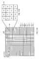
- the optical sensorcan include a 2D comb-array 1102 having multiple photosensitive elements 1104 arranged or grouped into cells 1106 , each cell having photosensitive elements grouped in a 4 ⁇ 4 elements-per-cell (or 4 ⁇ 4 elements/period) configuration.
- Photosensitive elements 1104 within a cell 1106 with the same letter and same number, as shown in the detail of FIG. 10B , as well as corresponding elements of all cells in the 2D comb-array 1102 with the same number,are electrically connected or wired-sum to yield eight group signals A 1 through D 2 .
- the eight wired-sum signalsare further combined or processed using a method of the present invention similar to that described above to detect and measure changes in phase of the signal from the array 1102 , which may then be used to produce ⁇ x, ⁇ y data providing information on the magnitude and direction of displacement of the optical sensor in x and y directions.
- photosensitive elements 1204 within a cell 1206can be grouped along horizontal, vertical and/or diagonal axes as shown in FIGS. 12A through 12D . Signals from photosensitive elements 1204 grouped along parallel axes within the cell 1206 and the array can be combined and the resultant signals processed using a method similar to that described above.
- FIGS. 12A through 12DSignals from photosensitive elements 1204 grouped along parallel axes within the cell 1206 and the array can be combined and the resultant signals processed using a method similar to that described above.
Landscapes
- Engineering & Computer Science (AREA)
- General Engineering & Computer Science (AREA)
- Theoretical Computer Science (AREA)
- Human Computer Interaction (AREA)
- Physics & Mathematics (AREA)
- General Physics & Mathematics (AREA)
- Position Input By Displaying (AREA)
- Navigation (AREA)
Abstract
Description
A′i=Ai−Amin (Eq. 2.0)
| TABLE I | |||||||
| If Aminis at: | θ0 | θ1 | θ2 | θ3 | θ4 | ||
| A0 | 0 | 72 | 144 | 216 | 288 | ||
| A1 | 0 | 72 | −216 | −144 | −72 | ||
| A2 | 0 | 72 | 144 | −144 | −72 | ||
| A3 | 0 | 72 | 144 | 216 | −72 | ||
| A4 | 0 | 72 | 144 | 216 | 288 | ||
Claims (14)
Priority Applications (1)
| Application Number | Priority Date | Filing Date | Title |
|---|---|---|---|
| US11/268,898US7248345B2 (en) | 2004-11-12 | 2005-11-08 | Signal processing method for use with an optical navigation system |
Applications Claiming Priority (2)
| Application Number | Priority Date | Filing Date | Title |
|---|---|---|---|
| US62722504P | 2004-11-12 | 2004-11-12 | |
| US11/268,898US7248345B2 (en) | 2004-11-12 | 2005-11-08 | Signal processing method for use with an optical navigation system |
Publications (2)
| Publication Number | Publication Date |
|---|---|
| US20060106319A1 US20060106319A1 (en) | 2006-05-18 |
| US7248345B2true US7248345B2 (en) | 2007-07-24 |
Family
ID=36337265
Family Applications (1)
| Application Number | Title | Priority Date | Filing Date |
|---|---|---|---|
| US11/268,898Active2026-02-17US7248345B2 (en) | 2004-11-12 | 2005-11-08 | Signal processing method for use with an optical navigation system |
Country Status (2)
| Country | Link |
|---|---|
| US (1) | US7248345B2 (en) |
| WO (1) | WO2006053234A2 (en) |
Cited By (19)
| Publication number | Priority date | Publication date | Assignee | Title |
|---|---|---|---|---|
| US20050259098A1 (en)* | 2004-05-21 | 2005-11-24 | Silicon Light Machines Corporation | Optical positioning device using telecentric imaging |
| US20060118743A1 (en)* | 2004-12-02 | 2006-06-08 | Silicon Light Machines Corporation | Signal processing method for optical sensors |
| US20070111111A1 (en)* | 2005-11-15 | 2007-05-17 | Yokogawa Electric Corporation | Light measurement apparatus and light measurement method |
| US20070139381A1 (en)* | 2005-12-20 | 2007-06-21 | Spurlock Brett A | Speckle navigation system |
| US20070138377A1 (en)* | 2005-12-16 | 2007-06-21 | Silicon Light Machines Corporation | Optical navigation system having a filter-window to seal an enclosure thereof |
| US20070241262A1 (en)* | 2006-04-18 | 2007-10-18 | Kye Systems Corp. | Optical sensing unit for an optical input device |
| US20080007526A1 (en)* | 2006-07-10 | 2008-01-10 | Yansun Xu | Optical navigation sensor with variable tracking resolution |
| US20080043223A1 (en)* | 2006-08-18 | 2008-02-21 | Atlab Inc. | Optical navigation device and method for compensating for offset in optical navigation device |
| US20090040062A1 (en)* | 2007-08-06 | 2009-02-12 | Lang Robert J | Processing methods for speckle-based motion sensing |
| US20100020011A1 (en)* | 2008-07-23 | 2010-01-28 | Sony Corporation | Mapping detected movement of an interference pattern of a coherent light beam to cursor movement to effect navigation of a user interface |
| US7721609B2 (en) | 2006-03-31 | 2010-05-25 | Cypress Semiconductor Corporation | Method and apparatus for sensing the force with which a button is pressed |
| US7723659B1 (en) | 2008-10-10 | 2010-05-25 | Cypress Semiconductor Corporation | System and method for screening semiconductor lasers |
| US7755604B2 (en) | 2006-06-19 | 2010-07-13 | Cypress Semiconductor Corporation | Optical navigation sensor with tracking and lift detection for optically transparent contact surfaces |
| US7884801B1 (en) | 2006-02-16 | 2011-02-08 | Cypress Semiconductor Corporation | Circuit and method for determining motion with redundant comb-arrays |
| US8072429B2 (en) | 2006-12-22 | 2011-12-06 | Cypress Semiconductor Corporation | Multi-axial touch-sensor device with multi-touch resolution |
| US20120087571A1 (en)* | 2010-10-08 | 2012-04-12 | Electronics And Telecommunications Research Institute | Method and apparatus for synchronizing 3-dimensional image |
| US8217334B1 (en) | 2008-12-24 | 2012-07-10 | Cypress Semiconductor Corporation | Optical navigation sensor including a spatial frequency filter |
| US8541727B1 (en) | 2008-09-30 | 2013-09-24 | Cypress Semiconductor Corporation | Signal monitoring and control system for an optical navigation sensor |
| US8711096B1 (en) | 2009-03-27 | 2014-04-29 | Cypress Semiconductor Corporation | Dual protocol input device |
Families Citing this family (3)
| Publication number | Priority date | Publication date | Assignee | Title |
|---|---|---|---|---|
| US7268341B2 (en)* | 2004-05-21 | 2007-09-11 | Silicon Light Machines Corporation | Optical position sensing device including interlaced groups of photosensitive elements |
| US7138620B2 (en)* | 2004-10-29 | 2006-11-21 | Silicon Light Machines Corporation | Two-dimensional motion sensor |
| US10579193B2 (en)* | 2017-12-14 | 2020-03-03 | Cypress Semiconductor Corporation | Spatial-frequency-based capacitive motion sensor and method of using the same |
Citations (46)
| Publication number | Priority date | Publication date | Assignee | Title |
|---|---|---|---|---|
| US3922093A (en) | 1972-11-24 | 1975-11-25 | Bbc Brown Boveri & Cie | Device for measuring the roughness of a surface |
| US4546347A (en) | 1981-05-18 | 1985-10-08 | Mouse Systems Corporation | Detector for electro-optical mouse |
| US4799055A (en) | 1984-04-26 | 1989-01-17 | Symbolics Inc. | Optical Mouse |
| US5288993A (en) | 1992-10-05 | 1994-02-22 | Logitech, Inc. | Cursor pointing device utilizing a photodetector array with target ball having randomly distributed speckles |
| US5473344A (en) | 1994-01-06 | 1995-12-05 | Microsoft Corporation | 3-D cursor positioning device |
| US5578813A (en) | 1995-03-02 | 1996-11-26 | Allen; Ross R. | Freehand image scanning device which compensates for non-linear movement |
| US5703356A (en) | 1992-10-05 | 1997-12-30 | Logitech, Inc. | Pointing device utilizing a photodetector array |
| US5729009A (en) | 1992-10-05 | 1998-03-17 | Logitech, Inc. | Method for generating quasi-sinusoidal signals |
| US5729008A (en) | 1996-01-25 | 1998-03-17 | Hewlett-Packard Company | Method and device for tracking relative movement by correlating signals from an array of photoelements |
| US5786804A (en) | 1995-10-06 | 1998-07-28 | Hewlett-Packard Company | Method and system for tracking attitude |
| US5854482A (en) | 1992-10-05 | 1998-12-29 | Logitech, Inc. | Pointing device utilizing a photodector array |
| US5907152A (en) | 1992-10-05 | 1999-05-25 | Logitech, Inc. | Pointing device utilizing a photodetector array |
| US5994710A (en) | 1998-04-30 | 1999-11-30 | Hewlett-Packard Company | Scanning mouse for a computer system |
| US6031218A (en) | 1992-10-05 | 2000-02-29 | Logitech, Inc. | System and method for generating band-limited quasi-sinusoidal signals |
| US6037643A (en) | 1998-02-17 | 2000-03-14 | Hewlett-Packard Company | Photocell layout for high-speed optical navigation microchips |
| US6057540A (en) | 1998-04-30 | 2000-05-02 | Hewlett-Packard Co | Mouseless optical and position translation type screen pointer control for a computer system |
| US6097371A (en) | 1996-01-02 | 2000-08-01 | Microsoft Corporation | System and method of adjusting display characteristics of a displayable data file using an ergonomic computer input device |
| US6151015A (en) | 1998-04-27 | 2000-11-21 | Agilent Technologies | Pen like computer pointing device |
| US6172354B1 (en) | 1998-01-28 | 2001-01-09 | Microsoft Corporation | Operator input device |
| US6233368B1 (en) | 1998-03-18 | 2001-05-15 | Agilent Technologies, Inc. | CMOS digital optical navigation chip |
| US6326950B1 (en) | 1999-07-08 | 2001-12-04 | Primax Electronics Ltd. | Pointing device using two linear sensors and fingerprints to generate displacement signals |
| US6330057B1 (en) | 1998-03-09 | 2001-12-11 | Otm Technologies Ltd. | Optical translation measurement |
| US6351257B1 (en) | 1999-07-08 | 2002-02-26 | Primax Electronics Ltd. | Pointing device which uses an image picture to generate pointing signals |
| US6396479B2 (en) | 1998-07-31 | 2002-05-28 | Agilent Technologies, Inc. | Ergonomic computer mouse |
| US6421045B1 (en) | 2000-03-24 | 2002-07-16 | Microsoft Corporation | Snap-on lens carrier assembly for integrated chip optical sensor |
| US6424407B1 (en) | 1998-03-09 | 2002-07-23 | Otm Technologies Ltd. | Optical translation measurement |
| US6455840B1 (en) | 1999-10-28 | 2002-09-24 | Hewlett-Packard Company | Predictive and pulsed illumination of a surface in a micro-texture navigation technique |
| US6462330B1 (en) | 2000-03-24 | 2002-10-08 | Microsoft Corporation | Cover with integrated lens for integrated chip optical sensor |
| US6476970B1 (en) | 2000-08-10 | 2002-11-05 | Agilent Technologies, Inc. | Illumination optics and method |
| US6529184B1 (en) | 2000-03-22 | 2003-03-04 | Microsoft Corporation | Ball pattern architecture |
| US20030071750A1 (en)* | 2001-03-02 | 2003-04-17 | Benitz Gerald R. | High-definition imaging apparatus and method |
| US6585158B2 (en) | 2000-11-30 | 2003-07-01 | Agilent Technologies, Inc. | Combined pointing device and bar code scanner |
| US6603111B2 (en) | 2001-04-30 | 2003-08-05 | Agilent Technologies, Inc. | Image filters and source of illumination for optical navigation upon arbitrary surfaces are selected according to analysis of correlation during navigation |
| US6621483B2 (en) | 2001-03-16 | 2003-09-16 | Agilent Technologies, Inc. | Optical screen pointing device with inertial properties |
| US6657184B2 (en) | 2001-10-23 | 2003-12-02 | Agilent Technologies, Inc. | Optical navigation upon grainy surfaces using multiple navigation sensors |
| US6664948B2 (en) | 2001-07-30 | 2003-12-16 | Microsoft Corporation | Tracking pointing device motion using a single buffer for cross and auto correlation determination |
| US6674475B1 (en) | 1999-08-09 | 2004-01-06 | Agilent Technologies, Inc. | Method and circuit for electronic shutter control |
| US6677929B2 (en) | 2001-03-21 | 2004-01-13 | Agilent Technologies, Inc. | Optical pseudo trackball controls the operation of an appliance or machine |
| US6703599B1 (en) | 2002-01-30 | 2004-03-09 | Microsoft Corporation | Proximity sensor with adaptive threshold |
| US6774915B2 (en) | 2002-02-11 | 2004-08-10 | Microsoft Corporation | Pointing device reporting utilizing scaling |
| US6774351B2 (en) | 2001-05-25 | 2004-08-10 | Agilent Technologies, Inc. | Low-power surface for an optical sensor |
| US6795056B2 (en) | 2001-07-24 | 2004-09-21 | Agilent Technologies, Inc. | System and method for reducing power consumption in an optical screen pointing device |
| US6809723B2 (en) | 2001-05-14 | 2004-10-26 | Agilent Technologies, Inc. | Pushbutton optical screen pointing device |
| US6819314B2 (en) | 2002-11-08 | 2004-11-16 | Agilent Technologies, Inc. | Intensity flattener for optical mouse sensors |
| US6823077B2 (en) | 2001-07-30 | 2004-11-23 | Agilent Technologies, Inc. | Simplified interpolation for an optical navigation system that correlates images of one bit resolution |
| US7119323B1 (en)* | 2005-03-18 | 2006-10-10 | Avago Technologies Ecbu Ip (Singapore) Pte. Ltd. | Error corrected optical navigation system |
Family Cites Families (3)
| Publication number | Priority date | Publication date | Assignee | Title |
|---|---|---|---|---|
| US5031218A (en)* | 1988-03-30 | 1991-07-09 | International Business Machines Corporation | Redundant message processing and storage |
| US6161015A (en)* | 1998-05-28 | 2000-12-12 | Motorola, Inc. | Method for improving communication coverage in multi-cell communication systems using location information |
| US7043082B2 (en)* | 2000-01-06 | 2006-05-09 | Canon Kabushiki Kaisha | Demodulation and phase estimation of two-dimensional patterns |
- 2005
- 2005-11-08USUS11/268,898patent/US7248345B2/enactiveActive
- 2005-11-12WOPCT/US2005/040968patent/WO2006053234A2/enactiveApplication Filing
Patent Citations (56)
| Publication number | Priority date | Publication date | Assignee | Title |
|---|---|---|---|---|
| US3922093A (en) | 1972-11-24 | 1975-11-25 | Bbc Brown Boveri & Cie | Device for measuring the roughness of a surface |
| US4546347A (en) | 1981-05-18 | 1985-10-08 | Mouse Systems Corporation | Detector for electro-optical mouse |
| US4799055A (en) | 1984-04-26 | 1989-01-17 | Symbolics Inc. | Optical Mouse |
| US5854482A (en) | 1992-10-05 | 1998-12-29 | Logitech, Inc. | Pointing device utilizing a photodector array |
| US5288993A (en) | 1992-10-05 | 1994-02-22 | Logitech, Inc. | Cursor pointing device utilizing a photodetector array with target ball having randomly distributed speckles |
| US6225617B1 (en) | 1992-10-05 | 2001-05-01 | Logitech, Inc. | Method for generating quasi-sinusoidal signals |
| US6031218A (en) | 1992-10-05 | 2000-02-29 | Logitech, Inc. | System and method for generating band-limited quasi-sinusoidal signals |
| US5703356A (en) | 1992-10-05 | 1997-12-30 | Logitech, Inc. | Pointing device utilizing a photodetector array |
| US5729009A (en) | 1992-10-05 | 1998-03-17 | Logitech, Inc. | Method for generating quasi-sinusoidal signals |
| US5907152A (en) | 1992-10-05 | 1999-05-25 | Logitech, Inc. | Pointing device utilizing a photodetector array |
| US5963197A (en) | 1994-01-06 | 1999-10-05 | Microsoft Corporation | 3-D cursor positioning device |
| US5473344A (en) | 1994-01-06 | 1995-12-05 | Microsoft Corporation | 3-D cursor positioning device |
| US5825044A (en) | 1995-03-02 | 1998-10-20 | Hewlett-Packard Company | Freehand image scanning device which compensates for non-linear color movement |
| US5644139A (en) | 1995-03-02 | 1997-07-01 | Allen; Ross R. | Navigation technique for detecting movement of navigation sensors relative to an object |
| US5578813A (en) | 1995-03-02 | 1996-11-26 | Allen; Ross R. | Freehand image scanning device which compensates for non-linear movement |
| US5786804A (en) | 1995-10-06 | 1998-07-28 | Hewlett-Packard Company | Method and system for tracking attitude |
| US6281882B1 (en) | 1995-10-06 | 2001-08-28 | Agilent Technologies, Inc. | Proximity detector for a seeing eye mouse |
| US6433780B1 (en) | 1995-10-06 | 2002-08-13 | Agilent Technologies, Inc. | Seeing eye mouse for a computer system |
| US6097371A (en) | 1996-01-02 | 2000-08-01 | Microsoft Corporation | System and method of adjusting display characteristics of a displayable data file using an ergonomic computer input device |
| US6281881B1 (en) | 1996-01-02 | 2001-08-28 | Microsoft Corporation | System and method of adjusting display characteristics of a displayable data file using an ergonomic computer input device |
| US5729008A (en) | 1996-01-25 | 1998-03-17 | Hewlett-Packard Company | Method and device for tracking relative movement by correlating signals from an array of photoelements |
| US6172354B1 (en) | 1998-01-28 | 2001-01-09 | Microsoft Corporation | Operator input device |
| US6037643A (en) | 1998-02-17 | 2000-03-14 | Hewlett-Packard Company | Photocell layout for high-speed optical navigation microchips |
| US6424407B1 (en) | 1998-03-09 | 2002-07-23 | Otm Technologies Ltd. | Optical translation measurement |
| US6330057B1 (en) | 1998-03-09 | 2001-12-11 | Otm Technologies Ltd. | Optical translation measurement |
| US6452683B1 (en) | 1998-03-09 | 2002-09-17 | Otm Technologies Ltd. | Optical translation measurement |
| US6233368B1 (en) | 1998-03-18 | 2001-05-15 | Agilent Technologies, Inc. | CMOS digital optical navigation chip |
| US6151015A (en) | 1998-04-27 | 2000-11-21 | Agilent Technologies | Pen like computer pointing device |
| US6057540A (en) | 1998-04-30 | 2000-05-02 | Hewlett-Packard Co | Mouseless optical and position translation type screen pointer control for a computer system |
| US5994710A (en) | 1998-04-30 | 1999-11-30 | Hewlett-Packard Company | Scanning mouse for a computer system |
| US6396479B2 (en) | 1998-07-31 | 2002-05-28 | Agilent Technologies, Inc. | Ergonomic computer mouse |
| US6351257B1 (en) | 1999-07-08 | 2002-02-26 | Primax Electronics Ltd. | Pointing device which uses an image picture to generate pointing signals |
| US6326950B1 (en) | 1999-07-08 | 2001-12-04 | Primax Electronics Ltd. | Pointing device using two linear sensors and fingerprints to generate displacement signals |
| US6674475B1 (en) | 1999-08-09 | 2004-01-06 | Agilent Technologies, Inc. | Method and circuit for electronic shutter control |
| US6455840B1 (en) | 1999-10-28 | 2002-09-24 | Hewlett-Packard Company | Predictive and pulsed illumination of a surface in a micro-texture navigation technique |
| US6529184B1 (en) | 2000-03-22 | 2003-03-04 | Microsoft Corporation | Ball pattern architecture |
| US6421045B1 (en) | 2000-03-24 | 2002-07-16 | Microsoft Corporation | Snap-on lens carrier assembly for integrated chip optical sensor |
| US6462330B1 (en) | 2000-03-24 | 2002-10-08 | Microsoft Corporation | Cover with integrated lens for integrated chip optical sensor |
| US6476970B1 (en) | 2000-08-10 | 2002-11-05 | Agilent Technologies, Inc. | Illumination optics and method |
| US6585158B2 (en) | 2000-11-30 | 2003-07-01 | Agilent Technologies, Inc. | Combined pointing device and bar code scanner |
| US6608585B2 (en)* | 2001-03-02 | 2003-08-19 | Massachusetts Institute Of Technology | High-definition imaging apparatus and method |
| US20030071750A1 (en)* | 2001-03-02 | 2003-04-17 | Benitz Gerald R. | High-definition imaging apparatus and method |
| US6621483B2 (en) | 2001-03-16 | 2003-09-16 | Agilent Technologies, Inc. | Optical screen pointing device with inertial properties |
| US6677929B2 (en) | 2001-03-21 | 2004-01-13 | Agilent Technologies, Inc. | Optical pseudo trackball controls the operation of an appliance or machine |
| US6603111B2 (en) | 2001-04-30 | 2003-08-05 | Agilent Technologies, Inc. | Image filters and source of illumination for optical navigation upon arbitrary surfaces are selected according to analysis of correlation during navigation |
| US6737636B2 (en) | 2001-04-30 | 2004-05-18 | Agilent Technologies, Inc. | Image filters and source of illumination for optical navigation upon arbitrary surfaces are selected according to analysis of correlation during navigation |
| US6809723B2 (en) | 2001-05-14 | 2004-10-26 | Agilent Technologies, Inc. | Pushbutton optical screen pointing device |
| US6774351B2 (en) | 2001-05-25 | 2004-08-10 | Agilent Technologies, Inc. | Low-power surface for an optical sensor |
| US6795056B2 (en) | 2001-07-24 | 2004-09-21 | Agilent Technologies, Inc. | System and method for reducing power consumption in an optical screen pointing device |
| US6664948B2 (en) | 2001-07-30 | 2003-12-16 | Microsoft Corporation | Tracking pointing device motion using a single buffer for cross and auto correlation determination |
| US6823077B2 (en) | 2001-07-30 | 2004-11-23 | Agilent Technologies, Inc. | Simplified interpolation for an optical navigation system that correlates images of one bit resolution |
| US6657184B2 (en) | 2001-10-23 | 2003-12-02 | Agilent Technologies, Inc. | Optical navigation upon grainy surfaces using multiple navigation sensors |
| US6703599B1 (en) | 2002-01-30 | 2004-03-09 | Microsoft Corporation | Proximity sensor with adaptive threshold |
| US6774915B2 (en) | 2002-02-11 | 2004-08-10 | Microsoft Corporation | Pointing device reporting utilizing scaling |
| US6819314B2 (en) | 2002-11-08 | 2004-11-16 | Agilent Technologies, Inc. | Intensity flattener for optical mouse sensors |
| US7119323B1 (en)* | 2005-03-18 | 2006-10-10 | Avago Technologies Ecbu Ip (Singapore) Pte. Ltd. | Error corrected optical navigation system |
Cited By (31)
| Publication number | Priority date | Publication date | Assignee | Title |
|---|---|---|---|---|
| US20050259098A1 (en)* | 2004-05-21 | 2005-11-24 | Silicon Light Machines Corporation | Optical positioning device using telecentric imaging |
| US7773070B2 (en) | 2004-05-21 | 2010-08-10 | Cypress Semiconductor Corporation | Optical positioning device using telecentric imaging |
| US8345003B1 (en) | 2004-05-21 | 2013-01-01 | Cypress Semiconductor Corporation | Optical positioning device using telecentric imaging |
| US20060118743A1 (en)* | 2004-12-02 | 2006-06-08 | Silicon Light Machines Corporation | Signal processing method for optical sensors |
| US7435942B2 (en) | 2004-12-02 | 2008-10-14 | Cypress Semiconductor Corporation | Signal processing method for optical sensors |
| US20070111111A1 (en)* | 2005-11-15 | 2007-05-17 | Yokogawa Electric Corporation | Light measurement apparatus and light measurement method |
| US20070138377A1 (en)* | 2005-12-16 | 2007-06-21 | Silicon Light Machines Corporation | Optical navigation system having a filter-window to seal an enclosure thereof |
| US8558163B2 (en) | 2005-12-16 | 2013-10-15 | Cypress Semiconductor Corporation | Optical navigation system having a filter-window to seal an enclosure thereof |
| US8471191B2 (en) | 2005-12-16 | 2013-06-25 | Cypress Semiconductor Corporation | Optical navigation system having a filter-window to seal an enclosure thereof |
| US7737948B2 (en) | 2005-12-20 | 2010-06-15 | Cypress Semiconductor Corporation | Speckle navigation system |
| US20070139381A1 (en)* | 2005-12-20 | 2007-06-21 | Spurlock Brett A | Speckle navigation system |
| US8547336B1 (en) | 2006-02-16 | 2013-10-01 | Cypress Semiconductor Corporation | Circuit and method for determining motion with redundant comb-arrays |
| US7884801B1 (en) | 2006-02-16 | 2011-02-08 | Cypress Semiconductor Corporation | Circuit and method for determining motion with redundant comb-arrays |
| US7721609B2 (en) | 2006-03-31 | 2010-05-25 | Cypress Semiconductor Corporation | Method and apparatus for sensing the force with which a button is pressed |
| US20070241262A1 (en)* | 2006-04-18 | 2007-10-18 | Kye Systems Corp. | Optical sensing unit for an optical input device |
| US7755604B2 (en) | 2006-06-19 | 2010-07-13 | Cypress Semiconductor Corporation | Optical navigation sensor with tracking and lift detection for optically transparent contact surfaces |
| US20080007526A1 (en)* | 2006-07-10 | 2008-01-10 | Yansun Xu | Optical navigation sensor with variable tracking resolution |
| US7728816B2 (en) | 2006-07-10 | 2010-06-01 | Cypress Semiconductor Corporation | Optical navigation sensor with variable tracking resolution |
| US20080043223A1 (en)* | 2006-08-18 | 2008-02-21 | Atlab Inc. | Optical navigation device and method for compensating for offset in optical navigation device |
| US8179369B2 (en)* | 2006-08-18 | 2012-05-15 | Atlab Inc. | Optical navigation device and method for compensating for offset in optical navigation device |
| US8072429B2 (en) | 2006-12-22 | 2011-12-06 | Cypress Semiconductor Corporation | Multi-axial touch-sensor device with multi-touch resolution |
| US8263921B2 (en)* | 2007-08-06 | 2012-09-11 | Cypress Semiconductor Corporation | Processing methods for speckle-based motion sensing |
| US20090040062A1 (en)* | 2007-08-06 | 2009-02-12 | Lang Robert J | Processing methods for speckle-based motion sensing |
| US8451224B2 (en)* | 2008-07-23 | 2013-05-28 | Sony Corporation | Mapping detected movement of an interference pattern of a coherent light beam to cursor movement to effect navigation of a user interface |
| US20100020011A1 (en)* | 2008-07-23 | 2010-01-28 | Sony Corporation | Mapping detected movement of an interference pattern of a coherent light beam to cursor movement to effect navigation of a user interface |
| US8541727B1 (en) | 2008-09-30 | 2013-09-24 | Cypress Semiconductor Corporation | Signal monitoring and control system for an optical navigation sensor |
| US8541728B1 (en) | 2008-09-30 | 2013-09-24 | Cypress Semiconductor Corporation | Signal monitoring and control system for an optical navigation sensor |
| US7723659B1 (en) | 2008-10-10 | 2010-05-25 | Cypress Semiconductor Corporation | System and method for screening semiconductor lasers |
| US8217334B1 (en) | 2008-12-24 | 2012-07-10 | Cypress Semiconductor Corporation | Optical navigation sensor including a spatial frequency filter |
| US8711096B1 (en) | 2009-03-27 | 2014-04-29 | Cypress Semiconductor Corporation | Dual protocol input device |
| US20120087571A1 (en)* | 2010-10-08 | 2012-04-12 | Electronics And Telecommunications Research Institute | Method and apparatus for synchronizing 3-dimensional image |
Also Published As
| Publication number | Publication date |
|---|---|
| WO2006053234A3 (en) | 2007-08-23 |
| US20060106319A1 (en) | 2006-05-18 |
| WO2006053234A2 (en) | 2006-05-18 |
Similar Documents
| Publication | Publication Date | Title |
|---|---|---|
| US7248345B2 (en) | Signal processing method for use with an optical navigation system | |
| US7297912B1 (en) | Circuit and method for reducing power consumption in an optical navigation system having redundant arrays | |
| US7138620B2 (en) | Two-dimensional motion sensor | |
| US7728816B2 (en) | Optical navigation sensor with variable tracking resolution | |
| US7042575B2 (en) | Speckle sizing and sensor dimensions in optical positioning device | |
| KR100816139B1 (en) | Optical positioning device with multi-row detector array | |
| US20050190157A1 (en) | Data input device and method for detecting an off-surface condition by a laser speckle size characteristic | |
| US7268341B2 (en) | Optical position sensing device including interlaced groups of photosensitive elements | |
| TWI269019B (en) | Optical positioning device using different combinations of interlaced photosensitive elements | |
| US7298460B2 (en) | Method for determining motion using a velocity predictor | |
| US20050258346A1 (en) | Optical positioning device resistant to speckle fading | |
| US8547336B1 (en) | Circuit and method for determining motion with redundant comb-arrays | |
| US7405389B2 (en) | Dense multi-axis array for motion sensing | |
| TWI472959B (en) | Processing methods for speckle-based motion sensing | |
| US8541728B1 (en) | Signal monitoring and control system for an optical navigation sensor | |
| CN110307785B (en) | Method, device and system for precise positioning of spot position based on memory effect | |
| CN100530315C (en) | Optical positioning device using telecentric imaging | |
| JP2008500557A (en) | Speckle sizing and sensor dimensions in optical positioning devices | |
| JPH07286815A (en) | Position detector |
Legal Events
| Date | Code | Title | Description |
|---|---|---|---|
| AS | Assignment | Owner name:SILICON LIGHT MACHINES CORPORATION, CALIFORNIA Free format text:ASSIGNMENT OF ASSIGNORS INTEREST;ASSIGNORS:TODOROFF, BRIAN D.;XU, YANSUN;REEL/FRAME:017208/0919 Effective date:20051107 | |
| STCF | Information on status: patent grant | Free format text:PATENTED CASE | |
| AS | Assignment | Owner name:CYPRESS SEMICONDUCTOR CORPORATION, CALIFORNIA Free format text:ASSIGNMENT OF ASSIGNORS INTEREST;ASSIGNOR:SILICON LIGHT MACHINES CORPORATION;REEL/FRAME:020897/0892 Effective date:20080417 | |
| FEPP | Fee payment procedure | Free format text:PAYOR NUMBER ASSIGNED (ORIGINAL EVENT CODE: ASPN); ENTITY STATUS OF PATENT OWNER: LARGE ENTITY | |
| REMI | Maintenance fee reminder mailed | ||
| FPAY | Fee payment | Year of fee payment:4 | |
| SULP | Surcharge for late payment | ||
| FPAY | Fee payment | Year of fee payment:8 | |
| AS | Assignment | Owner name:MORGAN STANLEY SENIOR FUNDING, INC., NEW YORK Free format text:SECURITY INTEREST;ASSIGNORS:CYPRESS SEMICONDUCTOR CORPORATION;SPANSION LLC;REEL/FRAME:035240/0429 Effective date:20150312 | |
| MAFP | Maintenance fee payment | Free format text:PAYMENT OF MAINTENANCE FEE, 12TH YEAR, LARGE ENTITY (ORIGINAL EVENT CODE: M1553); ENTITY STATUS OF PATENT OWNER: LARGE ENTITY Year of fee payment:12 | |
| AS | Assignment | Owner name:MUFG UNION BANK, N.A., CALIFORNIA Free format text:ASSIGNMENT AND ASSUMPTION OF SECURITY INTEREST IN INTELLECTUAL PROPERTY;ASSIGNOR:MORGAN STANLEY SENIOR FUNDING, INC.;REEL/FRAME:050896/0366 Effective date:20190731 | |
| AS | Assignment | Owner name:MORGAN STANLEY SENIOR FUNDING, INC., NEW YORK Free format text:CORRECTIVE ASSIGNMENT TO CORRECT THE 8647899 PREVIOUSLY RECORDED ON REEL 035240 FRAME 0429. ASSIGNOR(S) HEREBY CONFIRMS THE SECURITY INTERST;ASSIGNORS:CYPRESS SEMICONDUCTOR CORPORATION;SPANSION LLC;REEL/FRAME:058002/0470 Effective date:20150312 | |
| AS | Assignment | Owner name:SPANSION LLC, CALIFORNIA Free format text:RELEASE BY SECURED PARTY;ASSIGNOR:MUFG UNION BANK, N.A.;REEL/FRAME:059410/0438 Effective date:20200416 Owner name:CYPRESS SEMICONDUCTOR CORPORATION, CALIFORNIA Free format text:RELEASE BY SECURED PARTY;ASSIGNOR:MUFG UNION BANK, N.A.;REEL/FRAME:059410/0438 Effective date:20200416 |