US7247851B2 - Imaging device and an imaging method - Google Patents
Imaging device and an imaging methodDownload PDFInfo
- Publication number
- US7247851B2 US7247851B2US10/533,853US53385305AUS7247851B2US 7247851 B2US7247851 B2US 7247851B2US 53385305 AUS53385305 AUS 53385305AUS 7247851 B2US7247851 B2US 7247851B2
- Authority
- US
- United States
- Prior art keywords
- near infrared
- visible light
- infrared light
- light
- pixels
- Prior art date
- Legal status (The legal status is an assumption and is not a legal conclusion. Google has not performed a legal analysis and makes no representation as to the accuracy of the status listed.)
- Expired - Lifetime, expires
Links
Images


Classifications
- H—ELECTRICITY
- H04—ELECTRIC COMMUNICATION TECHNIQUE
- H04N—PICTORIAL COMMUNICATION, e.g. TELEVISION
- H04N23/00—Cameras or camera modules comprising electronic image sensors; Control thereof
- H04N23/10—Cameras or camera modules comprising electronic image sensors; Control thereof for generating image signals from different wavelengths
- H04N23/11—Cameras or camera modules comprising electronic image sensors; Control thereof for generating image signals from different wavelengths for generating image signals from visible and infrared light wavelengths
- H—ELECTRICITY
- H04—ELECTRIC COMMUNICATION TECHNIQUE
- H04N—PICTORIAL COMMUNICATION, e.g. TELEVISION
- H04N25/00—Circuitry of solid-state image sensors [SSIS]; Control thereof
- H04N25/10—Circuitry of solid-state image sensors [SSIS]; Control thereof for transforming different wavelengths into image signals
- H04N25/11—Arrangement of colour filter arrays [CFA]; Filter mosaics
- H04N25/13—Arrangement of colour filter arrays [CFA]; Filter mosaics characterised by the spectral characteristics of the filter elements
- H04N25/131—Arrangement of colour filter arrays [CFA]; Filter mosaics characterised by the spectral characteristics of the filter elements including elements passing infrared wavelengths
- H—ELECTRICITY
- H04—ELECTRIC COMMUNICATION TECHNIQUE
- H04N—PICTORIAL COMMUNICATION, e.g. TELEVISION
- H04N25/00—Circuitry of solid-state image sensors [SSIS]; Control thereof
- H04N25/10—Circuitry of solid-state image sensors [SSIS]; Control thereof for transforming different wavelengths into image signals
- H04N25/17—Colour separation based on photon absorption depth, e.g. full colour resolution obtained simultaneously at each pixel location
- H—ELECTRICITY
- H10—SEMICONDUCTOR DEVICES; ELECTRIC SOLID-STATE DEVICES NOT OTHERWISE PROVIDED FOR
- H10F—INORGANIC SEMICONDUCTOR DEVICES SENSITIVE TO INFRARED RADIATION, LIGHT, ELECTROMAGNETIC RADIATION OF SHORTER WAVELENGTH OR CORPUSCULAR RADIATION
- H10F30/00—Individual radiation-sensitive semiconductor devices in which radiation controls the flow of current through the devices, e.g. photodetectors
- H10F30/20—Individual radiation-sensitive semiconductor devices in which radiation controls the flow of current through the devices, e.g. photodetectors the devices having potential barriers, e.g. phototransistors
- H10F30/21—Individual radiation-sensitive semiconductor devices in which radiation controls the flow of current through the devices, e.g. photodetectors the devices having potential barriers, e.g. phototransistors the devices being sensitive to infrared, visible or ultraviolet radiation
- H—ELECTRICITY
- H10—SEMICONDUCTOR DEVICES; ELECTRIC SOLID-STATE DEVICES NOT OTHERWISE PROVIDED FOR
- H10F—INORGANIC SEMICONDUCTOR DEVICES SENSITIVE TO INFRARED RADIATION, LIGHT, ELECTROMAGNETIC RADIATION OF SHORTER WAVELENGTH OR CORPUSCULAR RADIATION
- H10F39/00—Integrated devices, or assemblies of multiple devices, comprising at least one element covered by group H10F30/00, e.g. radiation detectors comprising photodiode arrays
- H10F39/10—Integrated devices
- H10F39/12—Image sensors
- H10F39/18—Complementary metal-oxide-semiconductor [CMOS] image sensors; Photodiode array image sensors
- H10F39/182—Colour image sensors
- H—ELECTRICITY
- H04—ELECTRIC COMMUNICATION TECHNIQUE
- H04N—PICTORIAL COMMUNICATION, e.g. TELEVISION
- H04N2209/00—Details of colour television systems
- H04N2209/04—Picture signal generators
- H04N2209/041—Picture signal generators using solid-state devices
- H04N2209/042—Picture signal generators using solid-state devices having a single pick-up sensor
- H04N2209/047—Picture signal generators using solid-state devices having a single pick-up sensor using multispectral pick-up elements
Definitions
- the present inventionrelates to an imaging device and imaging method for detecting and receiving three components of visible light and near infrared light in different wavelength regions and for imaging pictures of both visible light and near infrared light.
- each of pixelscan detect one of three colors of different wavelengths in visible light and near infrared light and such pixels are arranged in a mixed manner in the same imaging element, for example a CCD or CMOS imaging element (e.g. see FIG. 2 of Japanese Patent Laid-Open Application No. 2002-142228).
- a CCD or CMOS imaging elemente.g. see FIG. 2 of Japanese Patent Laid-Open Application No. 2002-142228.
- Mg (magenta) color detectors 81 , Ye (yellow) color detectors 82 , Cy (cyan) color detectors 83 , and near infrared light detectors 84are arranged on an imaging element like amosaic so that the combination repeats lengthwise and crosswise.
- one detectorcorresponds to just one pixel.
- a bare pixelhas a property of detecting visible light and near infrared light of 400 nm to 1000 nm.
- an Mg color detector 81is composed of a pixel covered with a bandpass filter for the region of the Mg color.
- the Ye color detectors 82 and Cy color detectors 83are also composed of pixels covered with bandpass filters which derive the regions of their respective wavelengths. Bare pixels are arranged as the near infrared light detectors 84 .
- the visible light regionrequires to be cut off. But it need not be cut off because obtaining luminance information will suffice.
- the above configurationallows imaging pictures of both visible light and near infrared light.
- three photodiodesare formed on a silicon substrate at different depths from the surface.
- This conventional deviceuses absorbance differences in silicon among three kinds of light of different wavelengths in the visible light region, e.g. blue, green, and red, to detect the three kinds of light of different wavelengths (e.g. see FIGS. 5 and 6 of Published Japanese Translation of PCT International Application (Tokuhyo) No. 2002-513145).
- three photodiodes of different depthscan be arranged in one pixel.
- This prior artcan therefore enable higher color resolution and prevent degradation of image quality caused by false color, in comparison with an art in which one pixel detects one color.
- FIG. 11shows the structure of a pixel formed on an imaging element.
- An n-type doped region 92 of an n-type semiconductoris formed on a p-type semiconductor substrate 91 .
- a p-type doped region 93is formed thereon.
- an n-type doped region 94is formed thereon.
- a three-layer semiconductor structuretriple-well structure
- blue lightis absorbed at a depth of 0.2 ⁇ m in a silicon layer.
- Greenis absorbed at 0.6 ⁇ m, and red is not absorbed until it reaches a depth of 2 ⁇ m.
- depths of interfaceswhich work as photosensors for each light, are set to 0.2 ⁇ m, 0.6 ⁇ m, and 2 ⁇ m respectively.
- Three colors (three wavelength bands) of lightcan thus be taken out almost spectrally. Then, an electric current generated by blue light is detected by a current detector 95 .
- the above-mentioned three-layer semiconductor doping structureallows one pixel to take out three colors of visible light and can realize a visible light imaging device with significantly improved color resolution.
- an optical systemcomprising optical lenses commonly provides an image of a subject on the surface of an imaging element. Since focuses fundamentally differ depending on wavelengths, chromatic aberration occurs in imaged pictures (when one color comes into focus, the others go out of focus). So, as shown in FIG. 12 , for example, an optical system having a property of an achromatic lens is commonly provided so that an imaging element is within the depth of focus (color shift is negligible within the range) with regard to magenta, yellow, and cyan in the visible light region, and the optical system therefore focuses.
- a purpose of the inventionis to provide an excellent visible light and near infrared light imaging device and method which can obtain clear color images with good color reproducibility by a visible light detection means and can at the same time obtain clear luminance information or monochrome images by a near infrared light detection means.
- the imaging device related to the inventioncomprises: an optical system means in which three components of visible light and near infrared light in different wavelength regions severally (or respectively) form images at different locations according to their wavelengths; and an imaging element which has a plurality of pixels; wherein said plurality of pixels include pixels having a visible light detection means and pixels having a near infrared light detection means, said visible light detection means detecting said three components of visible light which form images at locations of different depths in the same pixel according to their wavelengths, said near infrared light detection means detecting near infrared light which forms an image in a pixel at a location of a depth different from the depths at which said three components of visible light form images.
- the visible light detection meanshas three detectors which are provided at locations of different depths according to wavelength dependence of light absorption depth and detect visible light in three different wavelength regions of blue, green, and red
- the near infrared light detection meanshas a detector which is provided at a location of a depth different from the depths of the three detectors and detects near infrared light.
- clear color images with good color reproducibilitycan be obtained by a visible light detection means and at the same time clear luminance information or monochrome images can be obtained by a near infrared light detection means.
- color images with good color reproducibility and high color resolutioncan be provided in the daytime; sharp monochrome images can be obtained even in a dark place, e.g. nighttime, by shining some light; and, moreover, composites of those images can equivalently increase the dynamic range.
- An excellent imaging devicecan thus be provided.
- the imaging elementhas a configuration in which pixels having the visible light detection means and pixels having the near infrared light detection means are alternately arranged in rows and columns.
- the imaging elementhas a configuration in which pixels having the visible light detection means and pixels having the near infrared light detection means are uniformly arranged such that the number ratio of the pixels is one to three.
- the imaging elementhas a configuration in which pixels having the visible light detection means and pixels having the near infrared light detection means are uniformly arranged such that the area ratio of the pixels is one to three.
- two kinds of pixelsare arranged such that the number ratio or area ratio is one to three, so that luminance resolution, rather than color resolution, can be improved and clear luminance information of a range up to the near infrared light region can be obtained.
- An imaging device of another aspect of the inventioncomprises: an optical system means in which three components of visible light and near infrared light in different wavelength regions severally form images at different locations according to their wavelengths; and an imaging element which has a plurality of pixels; wherein the plurality of pixels have a detection means which detects the three components of visible light and the near infrared light which severally form images at locations of different depths in the same pixel according to their wavelengths.
- the plurality of pixelscomprise a detection means which detects three components of visible light of blue, green, and red and near infrared light by means of four detectors which are provided at locations of different depths according to wavelength dependence of light absorption depth.
- the optical system meanshas a configuration in which a focal length monotonously increases according to wavelengths of light from short-wavelength visible light to near infrared light so that visible light in three different wavelength regions of blue, green, and red and near infrared light form images at different locations.
- an imaging method related to the inventioncomprises: making three components of visible light and near infrared light in different wavelength regions severally form images at different locations according to their wavelengths; detecting the three components of visible light and the near infrared light using the fact that wavelength dependence of light absorption depth varies; and imaging pictures of both the three components of visible light and the near infrared light.
- FIG. 1illustrates a visible light and near infrared light imaging device and method related to the invention, and shows the essence of an optical system of the invention.
- FIG. 2shows the relation between the focal length of the optical system related to the invention and wavelengths.
- FIG. 3shows a configuration of an imaging element related to a first embodiment of the invention.
- FIG. 4shows a configuration of an imaging element related to the first embodiment of the invention.
- FIG. 5is an equivalent circuit schematic of an imaging element related to the first embodiment of the invention.
- FIG. 6shows an example of a mixed arrangement of visible light detection sections and near infrared light detection sections on an imaging element related to the first embodiment of the invention.
- FIG. 7shows an example of a mixed arrangement of visible light detection sections and near infrared light detection sections on an imaging element related to the first embodiment of the invention.
- FIG. 8shows a configuration of an imaging element related to a second embodiment of the invention.
- FIG. 9is an equivalent circuit schematic of an imaging element related to the second embodiment of the invention.
- FIG. 10shows an example of an imaging element of a conventional visible light and near infrared light imaging device.
- FIG. 11shows an example of an imaging element of a conventional visible light imaging device.
- FIG. 12illustrates an achromatic optical system used in a conventional visible light imaging device.
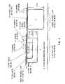
- a visible light and near infrared light imaging device related to the inventionhas an optical lens 1 .
- the optical lens 1is an optical system whose focal length is variable according to wavelengths, and makes three components of visible light and near infrared light in different wavelength regions form images at different locations according to their wavelengths.
- the optical lens 1condenses light from an external subject and forms an image on an imaging element 2 .
- light pencils from the optical lens 1are shown separately by different wavelengths.
- the optical lens 1forms images at different locations according to wavelengths as described above. This is shown more specifically in FIG. 2 .
- the focal length of the optical lens 1increases according to wavelengths, from that of short-wavelength light in visible light to near infrared light, and therefore three components of visible light and near infrared light form images at different locations.
- the imaging element 2composes a light receiving section together with the optical lens 1 qua an optical system.
- FIG. 3schematically shows the configuration of the imaging element 2 .
- visible light detection sections 6 and near infrared light detection sections 8are arranged in the imaging element 2 .
- the visible light detection section 6comprises three detectors of different depths, and it detects with these three detectors three components of visible light in different wavelength regions which are condensed by the optical lens 1 and form images, using the fact that wavelength dependence of light absorption depth varies.
- the near infrared light detection section 8has a detector which detects near infrared light.
- the visible light detection section 6is composed of a blue detector 3 , a green detector 4 , and a red detector 5 . These detectors 3 to 5 are photodiodes located at different depths from the surface. Three primary colors are obtained separately, so that any color is reproducible. Unlike the conventional Japanese Patent Laid-Open Application No. 2002-142228, one pixel can obtain output of three colors in visible light. As described in explanations of conventional arts, it is actually impossible to separate light into three colors completely. But a degree of mixing of each color is known (or can be measured) in advance, so corrections can be made.
- the infrared light detection section 8is composed of a near infrared light detector 7 , which is a photodiode.
- the near infrared light detector 7is located around the depth of the highest detectability.
- near infrared lightis absorbed at a depth deeper than red light in a silicon layer. So, the near infrared light detector 7 is located, for example, at the depth of 10 ⁇ m.
- Luminance informationcan be obtained from the visible light detector 6 by combining three colors with one another. If output from the near infrared light detector 7 is to be in proportion to overall light intensity, output from the near infrared light detector 7 may be used as luminance information.
- FIG. 4shows the configuration of the imaging element 2 related to the first embodiment.
- the configuration of the visible light detection section 6 on the left of the figureis almost similar to the conventional example.
- An n-type doped region 10 of an n-type semiconductoris formed on a p-type semiconductor substrate 9 .
- a p-type doped region 11is formed thereon.
- an n-type doped region 12is formed thereon.
- a three-layer semiconductor structure(triple-well structure) is made on the substrate.
- Three current detectors 14 , 15 , and 16detect output of B, G, and R of visible light. But if the three colors are somewhat influenced by near infrared light, colors reproduced later may be different from real colors.
- a near infrared light cut filter 13is placed in front of the light entrance to the current detectors. The influence of light in the near infrared region is thus eliminated.
- the near infrared light detection section 8 on the right of FIG. 4an n-type doped region 17 of an n-type semiconductor is formed additionally on the p-type semiconductor substrate 9 .
- the current detector 18detects a current when near infrared light comes in.
- the pn junction surfacethat is, the near infrared light detector 7 in FIG. 3 , is provided at the depth of 10 ⁇ m. In this way, the near infrared light detector 7 is located where detectability for near infrared light is the highest.
- near infrared lighthas a very wide wavelength range from 770 nm to 1000 nm. Accordingly, the above-mentioned value may vary depending on the purpose of detection, i.e. which wavelength region is to be mainly detected.
- optical lens 1described in FIGS. 1 and 2 , light in desired wavelength regions focuses on each detection area of the four current detectors 14 , 15 , 16 , and 18 .
- light of desired colorcomes into focus on a detection area of each detector.
- the optical lens 1is deliberately provided with aberration.
- FIG. 5shows an equivalent circuit schematic. As shown in FIG. 5 , each photodiode is reversely biased, and currents corresponding to incoming light are detected. In the interests of simplicity, power supply and grounds are common in the equivalent circuit schematic of FIG. 5 . However, the invention is not limited to this.
- FIGS. 6 and 7show examples of actual arrangements of visible light detection sections 6 and near infrared light detection sections 8 .
- visible light detection sections 6 and near infrared light detection sections 8are arranged in a mixed manner.
- a visible light detector 30composes the visible light detection section 6 and a near infrared light detector 31 composes the near infrared light detection section 8 .
- the visible light detectors 30 and the near infrared light detectors 31are alternately arranged in rows and columns in a mixed manner, and the ratio of the number or area of both pixels is one to one.
- an average for adjacent visible light detection sections 6may be taken.
- resolution of color informationmay be lower than luminance resolution assuming that the use is humans' seeing images.
- this arrangementhas higher resolution in both luminance and color than, for example, the conventional Japanese Patent Laid-Open Application No. 2002-142228.
- Output from the near infrared light detection section 8is useful as luminance information for detecting near infrared light in a relatively wide wavelength region.
- Sunlightespecially contains a lot of near infrared light components.
- luminance informationis obtained from adjacent near infrared light detection section 8 .
- information from the near infrared light detection section 8is used to correct output from the visible light detection section 6 .
- luminancecan usually be obtained by the following equation 1 when RGB is known.
- Y0.299 ⁇ R+ 0.587 ⁇ G+ 0.114 ⁇ B (1)
- luminanceis a linear sum of RGB.
- luminancemay be obtained by the following equation 2 when average luminance information I is derived from a plurality of adjacent near infrared light detection sections 8 .
- Yc 1 ⁇ R+c 2 ⁇ G+c 3 ⁇ B+c 4 ⁇ I (2)
- FIG. 7shows a configuration in which luminance information from near infrared light is actively used.
- the S/N ratio and resolution of luminance informationcan be improved.
- the visible light detector 30composes the visible light detection section 6
- the near infrared light detector 31composes the near infrared light detection section 8 .
- the visible light detectors 30 and the near infrared light detectors 31are alternately arranged in rows and columns in a mixed manner.
- the ratio of the number or area of visible light detection sections 6 to that of near infrared light detection sections 8is one to three in FIG. 7 .
- a set of one pixel of the visible light detection section 6 (visible light detector 30 ) and three pixels of the near infrared light detection sections (near infrared light detectors 31 )is arranged in a square, and the sets are arranged in rows and columns. In this way, they are uniformly arranged in the ratio of one to three.
- luminance resolutionrather than color resolution, can be improved. As a result, clear luminance information can be obtained for the range up to near infrared light.
- FIG. 8shows a configuration of an imaging element related to a second embodiment
- FIG. 9is an equivalent circuit schematic of an imaging element related to the second embodiment.
- a visible light detection section and near infrared light detection sectionare placed in one pixel.
- the figureshows one pixel, which comprises a detection section to separate and detect three components of visible light and near infrared light in different wavelength regions, four components in total.
- four current detectors 23 , 24 , 25 , and 26 arranged in one pixeldetect B, G, and R of visible light and near infrared light.
- an n-type doped region 19 of an n-type semiconductoris formed on a p-type semiconductor substrate 9 .
- a p-type doped region 20is formed thereon.
- an n-type doped region 21is formed thereon.
- a p-type doped region 22is formed thereon.
- a four-layer semiconductor structurequaddruple-well structure
- each pn interface regionfunctions as a photosensor, four photosensors can be made up in total.
- the depth of each interfacei.e. detection area, is determined and controlled as previously described. Light in four wavelength regions of blue, green, red, and near infrared light can thus be detected. Actually, it is difficult to separate four colors of light completely, and a mixture occurs. But a degree of mixing of each color is known (or can be measured) in advance, so corrections can be made.
- FIG. 9is an equivalent circuit schematic of FIG. 8 .
- Four photodiodesare reversely biased, and currents corresponding to incoming light are detected.
- power supply and groundsare common.
- the inventionis not limited to this.
- the mixing of visible light into near infrared lightis unavoidable.
- color reproducibilitymay be slightly worse in the second embodiment than in the first embodiment even if corrections are made.
- there is an advantage that resolution of both color and luminanceis better because one pixel simultaneously processes four colors.
- visible lightis separated into three wavelength regions in the embodiment, but it may be separated into four or more wavelength regions. In this case, good color images with higher color reproduction and resolution can be obtained.
Landscapes
- Engineering & Computer Science (AREA)
- Multimedia (AREA)
- Signal Processing (AREA)
- Physics & Mathematics (AREA)
- Spectroscopy & Molecular Physics (AREA)
- Transforming Light Signals Into Electric Signals (AREA)
- Solid State Image Pick-Up Elements (AREA)
- Color Television Image Signal Generators (AREA)
- Image Input (AREA)
- Facsimile Heads (AREA)
- Photometry And Measurement Of Optical Pulse Characteristics (AREA)
- Magnetic Resonance Imaging Apparatus (AREA)
- Electrotherapy Devices (AREA)
- Paper (AREA)
Abstract
Description
Y=0.299×R+0.587×G+0.114×B (1)
Y=c1×R+c2×G+c3×B+c4×I (2)
- (where c1+c2+c3+c4=1)
Claims (9)
Applications Claiming Priority (3)
| Application Number | Priority Date | Filing Date | Title |
|---|---|---|---|
| JP2003-380208 | 2003-11-10 | ||
| JP2003380208AJP4578797B2 (en) | 2003-11-10 | 2003-11-10 | Imaging device |
| PCT/JP2004/005799WO2005045936A1 (en) | 2003-11-10 | 2004-04-22 | Imaging device and imaging method |
Publications (2)
| Publication Number | Publication Date |
|---|---|
| US20060114551A1 US20060114551A1 (en) | 2006-06-01 |
| US7247851B2true US7247851B2 (en) | 2007-07-24 |
Family
ID=34567228
Family Applications (1)
| Application Number | Title | Priority Date | Filing Date |
|---|---|---|---|
| US10/533,853Expired - LifetimeUS7247851B2 (en) | 2003-11-10 | 2004-04-22 | Imaging device and an imaging method |
Country Status (7)
| Country | Link |
|---|---|
| US (1) | US7247851B2 (en) |
| EP (1) | EP1630871B1 (en) |
| JP (1) | JP4578797B2 (en) |
| CN (1) | CN100416843C (en) |
| AT (1) | ATE460748T1 (en) |
| DE (1) | DE602004025922D1 (en) |
| WO (1) | WO2005045936A1 (en) |
Cited By (31)
| Publication number | Priority date | Publication date | Assignee | Title |
|---|---|---|---|---|
| US20070284532A1 (en)* | 2006-06-13 | 2007-12-13 | Mitsubishi Electric Corporation | Two-wavelength image sensor picking up both visible and infrared images |
| US20080315104A1 (en)* | 2007-06-19 | 2008-12-25 | Maru Lsi Co., Ltd. | Color image sensing apparatus and method of processing infrared-ray signal |
| US20090159799A1 (en)* | 2007-12-19 | 2009-06-25 | Spectral Instruments, Inc. | Color infrared light sensor, camera, and method for capturing images |
| US20100102366A1 (en)* | 2008-10-24 | 2010-04-29 | Jong-Jan Lee | Integrated Infrared and Color CMOS Imager Sensor |
| US20100278212A1 (en)* | 2007-11-05 | 2010-11-04 | Burghartz Joachim N | Circuit arrangement and imaging pyrometer for generating light- and temperature-dependent signals |
| US8569700B2 (en)* | 2012-03-06 | 2013-10-29 | Omnivision Technologies, Inc. | Image sensor for two-dimensional and three-dimensional image capture |
| US20130320195A1 (en)* | 2012-06-01 | 2013-12-05 | Omnivision Technologies, Inc. | Lens array for partitioned image sensor |
| US8988566B2 (en) | 2012-08-09 | 2015-03-24 | Omnivision Technologies, Inc. | Lens array for partitioned image sensor having color filters |
| US9013620B2 (en) | 2011-04-20 | 2015-04-21 | Trw Automotive U.S. Llc | Multiple band imager and method |
| US9270953B2 (en) | 2014-05-16 | 2016-02-23 | Omnivision Technologies, Inc. | Wafer level camera having movable color filter grouping |
| US20170201662A1 (en)* | 2016-01-07 | 2017-07-13 | Samsung Electronics Co., Ltd. | Electronic device for providing thermal image and method thereof |
| US9721357B2 (en) | 2015-02-26 | 2017-08-01 | Dual Aperture International Co. Ltd. | Multi-aperture depth map using blur kernels and edges |
| US9829564B2 (en) | 2013-06-13 | 2017-11-28 | Basf Se | Detector for optically detecting at least one longitudinal coordinate of one object by determining a number of illuminated pixels |
| US9958535B2 (en) | 2013-08-19 | 2018-05-01 | Basf Se | Detector for determining a position of at least one object |
| US10012532B2 (en) | 2013-08-19 | 2018-07-03 | Basf Se | Optical detector |
| US10094927B2 (en) | 2014-09-29 | 2018-10-09 | Basf Se | Detector for optically determining a position of at least one object |
| US10120078B2 (en) | 2012-12-19 | 2018-11-06 | Basf Se | Detector having a transversal optical sensor and a longitudinal optical sensor |
| US10165203B2 (en)* | 2016-06-16 | 2018-12-25 | Intel Corporation | Per-pixel performance improvement for combined visible and infrared image sensor arrays |
| US10353049B2 (en) | 2013-06-13 | 2019-07-16 | Basf Se | Detector for optically detecting an orientation of at least one object |
| US10412283B2 (en) | 2015-09-14 | 2019-09-10 | Trinamix Gmbh | Dual aperture 3D camera and method using differing aperture areas |
| US10775505B2 (en) | 2015-01-30 | 2020-09-15 | Trinamix Gmbh | Detector for an optical detection of at least one object |
| US10890491B2 (en) | 2016-10-25 | 2021-01-12 | Trinamix Gmbh | Optical detector for an optical detection |
| US10948567B2 (en) | 2016-11-17 | 2021-03-16 | Trinamix Gmbh | Detector for optically detecting at least one object |
| US10955936B2 (en) | 2015-07-17 | 2021-03-23 | Trinamix Gmbh | Detector for optically detecting at least one object |
| US11041718B2 (en) | 2014-07-08 | 2021-06-22 | Basf Se | Detector for determining a position of at least one object |
| US11060922B2 (en) | 2017-04-20 | 2021-07-13 | Trinamix Gmbh | Optical detector |
| US11067692B2 (en) | 2017-06-26 | 2021-07-20 | Trinamix Gmbh | Detector for determining a position of at least one object |
| US11125880B2 (en) | 2014-12-09 | 2021-09-21 | Basf Se | Optical detector |
| US11211513B2 (en) | 2016-07-29 | 2021-12-28 | Trinamix Gmbh | Optical sensor and detector for an optical detection |
| US11428787B2 (en) | 2016-10-25 | 2022-08-30 | Trinamix Gmbh | Detector for an optical detection of at least one object |
| US11860292B2 (en) | 2016-11-17 | 2024-01-02 | Trinamix Gmbh | Detector and methods for authenticating at least one object |
Families Citing this family (62)
| Publication number | Priority date | Publication date | Assignee | Title |
|---|---|---|---|---|
| US7442629B2 (en) | 2004-09-24 | 2008-10-28 | President & Fellows Of Harvard College | Femtosecond laser-induced formation of submicrometer spikes on a semiconductor substrate |
| US7057256B2 (en) | 2001-05-25 | 2006-06-06 | President & Fellows Of Harvard College | Silicon-based visible and near-infrared optoelectric devices |
| JP4839632B2 (en)* | 2005-02-25 | 2011-12-21 | ソニー株式会社 | Imaging device |
| JP2006352466A (en)* | 2005-06-15 | 2006-12-28 | Fujitsu Ltd | Imaging device |
| JP4573769B2 (en) | 2005-12-20 | 2010-11-04 | 富士通セミコンダクター株式会社 | Image processing circuit and image processing method |
| KR100800310B1 (en)* | 2006-02-16 | 2008-02-01 | 마루엘에스아이 주식회사 | Optical sensing element capable of detecting visible light and infrared light and its manufacturing method |
| US7435961B2 (en)* | 2006-03-17 | 2008-10-14 | Lucent Technologies Inc. | Imaging sensor |
| KR101276757B1 (en) | 2006-05-26 | 2013-06-20 | 삼성전자주식회사 | Apparatus for photographing image and operating method for the same |
| KR20070115243A (en) | 2006-06-01 | 2007-12-05 | 삼성전자주식회사 | Image Imaging Apparatus, and Operation Method thereof |
| JP5045012B2 (en)* | 2006-07-20 | 2012-10-10 | 株式会社ニコン | Solid-state imaging device and imaging apparatus using the same |
| KR100818987B1 (en)* | 2006-09-19 | 2008-04-04 | 삼성전자주식회사 | An image pickup device and an operation method of the image pickup device |
| US7755117B2 (en) | 2006-12-12 | 2010-07-13 | Intersil Americas Inc. | Light sensors with infrared suppression |
| WO2008073783A2 (en)* | 2006-12-12 | 2008-06-19 | Intersil Americas Inc. | Light sensors with infrared suppression and use of the sensors for backlight control |
| US8456410B2 (en) | 2006-12-12 | 2013-06-04 | Intersil Americas Inc. | Backlight control using light sensors with infrared suppression |
| JP5012135B2 (en)* | 2007-03-28 | 2012-08-29 | コニカミノルタアドバンストレイヤー株式会社 | Ultra-deep image generator |
| KR100877069B1 (en) | 2007-04-23 | 2009-01-09 | 삼성전자주식회사 | Image Imaging Apparatus and Method |
| KR101316135B1 (en) | 2007-08-09 | 2013-10-08 | 엘지이노텍 주식회사 | Image signal processing method and image signal processor |
| KR100858034B1 (en)* | 2007-10-18 | 2008-09-10 | (주)실리콘화일 | Single chip vitality image sensor |
| CN101231193B (en)* | 2008-02-01 | 2010-06-09 | 中国电子科技集团公司第四十四研究所 | Monolithic Visible/Infrared Dual Spectrum Focal Plane Detector |
| JP5058040B2 (en)* | 2008-03-19 | 2012-10-24 | 株式会社東芝 | Solid-state imaging device |
| TWI356333B (en)* | 2008-03-21 | 2012-01-11 | Chimei Innolux Corp | Liquid crystal display and remote controlling syst |
| RU2383967C2 (en)* | 2008-04-10 | 2010-03-10 | Общество с ограниченной ответственностью ООО "Юник Ай Сиз" | Colour image photodetector matrix |
| KR101475464B1 (en)* | 2008-05-09 | 2014-12-22 | 삼성전자 주식회사 | Stacked Image Sensor |
| KR101503037B1 (en)* | 2008-10-23 | 2015-03-19 | 삼성전자주식회사 | Image sensor and its operation method |
| EP2180513A1 (en)* | 2008-10-27 | 2010-04-28 | Stmicroelectronics SA | Near infrared/color image sensor |
| JP5075795B2 (en)* | 2008-11-14 | 2012-11-21 | 株式会社東芝 | Solid-state imaging device |
| JP5353200B2 (en)* | 2008-11-20 | 2013-11-27 | ソニー株式会社 | Solid-state imaging device and imaging device |
| JP5299002B2 (en)* | 2009-03-23 | 2013-09-25 | ソニー株式会社 | Imaging device |
| US9673243B2 (en) | 2009-09-17 | 2017-06-06 | Sionyx, Llc | Photosensitive imaging devices and associated methods |
| US9911781B2 (en) | 2009-09-17 | 2018-03-06 | Sionyx, Llc | Photosensitive imaging devices and associated methods |
| US20110068426A1 (en)* | 2009-09-22 | 2011-03-24 | Intersil Americas Inc. | Photodiodes and methods for fabricating photodiodes |
| US8692198B2 (en) | 2010-04-21 | 2014-04-08 | Sionyx, Inc. | Photosensitive imaging devices and associated methods |
| JP2011229625A (en)* | 2010-04-26 | 2011-11-17 | Fujifilm Corp | Endoscopic system |
| JP2011229603A (en)* | 2010-04-26 | 2011-11-17 | Fujifilm Corp | Endoscopic system |
| JP2011239259A (en)* | 2010-05-12 | 2011-11-24 | Sony Corp | Image processing device, image processing method, and program |
| WO2011160130A2 (en) | 2010-06-18 | 2011-12-22 | Sionyx, Inc | High speed photosensitive devices and associated methods |
| JP2014514733A (en)* | 2011-03-10 | 2014-06-19 | サイオニクス、インク. | Three-dimensional sensor, system, and related methods |
| KR101241701B1 (en)* | 2011-04-11 | 2013-03-11 | 엘지이노텍 주식회사 | Pixel, pixel array and image sensor inclduding the pixel array |
| US9496308B2 (en) | 2011-06-09 | 2016-11-15 | Sionyx, Llc | Process module for increasing the response of backside illuminated photosensitive imagers and associated methods |
| KR101305885B1 (en)* | 2011-06-24 | 2013-09-06 | 엘지이노텍 주식회사 | Pixel, pixel array, image sensor including the same and method for operating the image sensor |
| WO2012174752A1 (en)* | 2011-06-24 | 2012-12-27 | 博立码杰通讯(深圳)有限公司 | Multi scene depth photo sensitive device, system thereof, scene depth expanding method, and optical imaging system |
| KR101220143B1 (en) | 2011-06-27 | 2013-01-11 | 어보브반도체 주식회사 | One-chip semiconductor apparatus for photo detectors with different receiving band and integrated circuit and manufacturing method thereof |
| WO2013010127A2 (en) | 2011-07-13 | 2013-01-17 | Sionyx, Inc. | Biometric imaging devices and associated methods |
| US9064764B2 (en) | 2012-03-22 | 2015-06-23 | Sionyx, Inc. | Pixel isolation elements, devices, and associated methods |
| EP2763397A1 (en)* | 2013-02-05 | 2014-08-06 | Burg-Wächter Kg | Photoelectric sensor |
| US9762830B2 (en) | 2013-02-15 | 2017-09-12 | Sionyx, Llc | High dynamic range CMOS image sensor having anti-blooming properties and associated methods |
| WO2014151093A1 (en) | 2013-03-15 | 2014-09-25 | Sionyx, Inc. | Three dimensional imaging utilizing stacked imager devices and associated methods |
| US9209345B2 (en) | 2013-06-29 | 2015-12-08 | Sionyx, Inc. | Shallow trench textured regions and associated methods |
| EP2871843B1 (en)* | 2013-11-12 | 2019-05-29 | LG Electronics Inc. -1- | Digital device and method for processing three dimensional image thereof |
| US10051211B2 (en)* | 2013-12-05 | 2018-08-14 | Omnivision Technologies, Inc. | Image sensors for capturing both visible light images and infrared light images, and associated systems and methods |
| WO2015097776A1 (en)* | 2013-12-25 | 2015-07-02 | 日立マクセル株式会社 | Image pickup element and image pickup apparatus |
| CN106030239B (en)* | 2014-01-29 | 2020-10-09 | Lg伊诺特有限公司 | Apparatus and method for extracting depth information |
| US10113903B1 (en)* | 2014-09-02 | 2018-10-30 | Amazon Technologies, Inc. | Ambient light sensor calibration |
| US20180003993A1 (en)* | 2014-12-09 | 2018-01-04 | Basf Se | Detector for an optical detection of at least one object |
| FR3030885B1 (en)* | 2014-12-22 | 2017-12-22 | E2V Semiconductors | COLOR IMAGE SENSOR WITH WHITE PIXELS AND COLOR PIXELS |
| CN105244357B (en)* | 2015-08-31 | 2018-06-26 | 上海集成电路研发中心有限公司 | Imaging detector pixel structure and preparation method thereof is mixed outside visible red |
| CN107146797B (en) | 2017-04-28 | 2020-03-27 | Oppo广东移动通信有限公司 | Dual-core focusing image sensor, focusing control method thereof and imaging device |
| CN108511542B (en)* | 2018-01-31 | 2020-05-19 | 中国科学院长春光学精密机械与物理研究所 | Photodiode of image sensor and image sensor |
| US10838489B2 (en)* | 2019-03-04 | 2020-11-17 | Microsoft Technology Licensing, Llc | IR illumination module for MEMS-based eye tracking |
| US11624906B2 (en) | 2019-03-04 | 2023-04-11 | Microsoft Technology Licensing, Llc | IR illumination module for MEMS-based eye tracking |
| US10832052B2 (en) | 2019-03-04 | 2020-11-10 | Microsoft Technology Licensing, Llc | IR illumination module for MEMS-based eye tracking |
| CN112770020A (en) | 2019-11-05 | 2021-05-07 | 北京小米移动软件有限公司 | Image sensing module, method, device, electronic device and medium |
Citations (31)
| Publication number | Priority date | Publication date | Assignee | Title |
|---|---|---|---|---|
| US3858046A (en)* | 1973-06-25 | 1974-12-31 | Hughes Aircraft Co | Catadioptric beamsplitter system |
| JPS5552277A (en) | 1978-10-06 | 1980-04-16 | Recognition Equipment Inc | Multiple spectrum photodiode device* photosensitive semiconductor device and method of manufacturing same |
| US4581625A (en) | 1983-12-19 | 1986-04-08 | Atlantic Richfield Company | Vertically integrated solid state color imager |
| JPS61187282A (en) | 1985-02-14 | 1986-08-20 | Mitsubishi Electric Corp | light detection element |
| US4677289A (en) | 1984-11-12 | 1987-06-30 | Kabushiki Kaisha Toshiba | Color sensor |
| JPH01134966A (en) | 1987-11-20 | 1989-05-26 | Fuji Photo Film Co Ltd | Solid-state image pickup device |
| JPH06205162A (en) | 1993-01-01 | 1994-07-22 | Canon Inc | Image reader |
| JPH0774340A (en) | 1993-09-01 | 1995-03-17 | Toshiba Corp | Solid-state imaging device |
| US5926238A (en)* | 1992-12-11 | 1999-07-20 | Canon Kabushiki Kaisha | Image display device, semiconductor device and optical element |
| US5965875A (en)* | 1998-04-24 | 1999-10-12 | Foveon, Inc. | Color separation in an active pixel cell imaging array using a triple-well structure |
| US6094281A (en)* | 1993-01-01 | 2000-07-25 | Canon Kabushiki Kaisha | Image reading device with offset faces for visible and non-visible light sensors |
| WO2000072604A1 (en) | 1999-05-21 | 2000-11-30 | Foveon, Inc. | Method for storing and retrieving digital image data from an imaging array |
| US6198147B1 (en)* | 1998-07-06 | 2001-03-06 | Intel Corporation | Detecting infrared and visible light |
| US6211521B1 (en)* | 1998-03-13 | 2001-04-03 | Intel Corporation | Infrared pixel sensor and infrared signal correction |
| US20010020677A1 (en)* | 1998-03-23 | 2001-09-13 | Kabushiki Kaisha Toshiba | Method and apparatus for reading invisible symbol |
| US20010043163A1 (en)* | 1996-03-15 | 2001-11-22 | Jonathan David Waldern | Method of and apparatus for viewing an image |
| WO2002027804A2 (en) | 2000-09-25 | 2002-04-04 | Foveon, Inc. | Vertical color filter detector group and array |
| US6380539B1 (en)* | 1997-01-30 | 2002-04-30 | Applied Science Fiction, Inc. | Four color trilinear CCD scanning |
| JP2002142228A (en) | 2000-10-31 | 2002-05-17 | Toyota Central Res & Dev Lab Inc | Imaging device |
| US20020131648A1 (en)* | 2001-03-13 | 2002-09-19 | Tadao Hayashide | Image processing apparatus and image processing method |
| US20020190254A1 (en) | 2001-06-18 | 2002-12-19 | Turner Richard M. | Vertical color filter detector group and array |
| US20030001093A1 (en)* | 2001-06-27 | 2003-01-02 | Honeywell Inc. | Sensor for dual wavelength bands |
| US20030132386A1 (en)* | 2002-01-14 | 2003-07-17 | William Carr | Micromachined pyro-optical structure |
| JP2003304548A (en) | 2002-04-10 | 2003-10-24 | Canon Inc | Imaging apparatus |
| US6759646B1 (en)* | 1998-11-24 | 2004-07-06 | Intel Corporation | Color interpolation for a four color mosaic pattern |
| US20040256561A1 (en)* | 2003-06-17 | 2004-12-23 | Allyson Beuhler | Wide band light sensing pixel array |
| US20050029456A1 (en)* | 2003-07-30 | 2005-02-10 | Helmuth Eggers | Sensor array with a number of types of optical sensors |
| US6998660B2 (en)* | 2002-03-20 | 2006-02-14 | Foveon, Inc. | Vertical color filter sensor group array that emulates a pattern of single-layer sensors with efficient use of each sensor group's sensors |
| US20060054987A1 (en)* | 2004-08-31 | 2006-03-16 | Fuji Photo Film Co., Ltd. | Photoelectric conversion device, image pickup device, and method for applying electric field to the same |
| US7129466B2 (en)* | 2002-05-08 | 2006-10-31 | Canon Kabushiki Kaisha | Color image pickup device and color light-receiving device |
| US7154157B2 (en)* | 2002-12-30 | 2006-12-26 | Intel Corporation | Stacked semiconductor radiation sensors having color component and infrared sensing capability |
Family Cites Families (2)
| Publication number | Priority date | Publication date | Assignee | Title |
|---|---|---|---|---|
| JPH07176708A (en)* | 1993-12-21 | 1995-07-14 | Matsushita Electron Corp | Solid-state image pickup device |
| JP2002151670A (en)* | 2000-08-30 | 2002-05-24 | Sony Corp | Solid-state image pickup device and manufacturing method |
- 2003
- 2003-11-10JPJP2003380208Apatent/JP4578797B2/ennot_activeExpired - Lifetime
- 2004
- 2004-04-22DEDE602004025922Tpatent/DE602004025922D1/ennot_activeExpired - Lifetime
- 2004-04-22ATAT04728931Tpatent/ATE460748T1/ennot_activeIP Right Cessation
- 2004-04-22EPEP04728931Apatent/EP1630871B1/ennot_activeExpired - Lifetime
- 2004-04-22CNCNB2004800007772Apatent/CN100416843C/ennot_activeExpired - Lifetime
- 2004-04-22WOPCT/JP2004/005799patent/WO2005045936A1/ennot_activeCeased
- 2004-04-22USUS10/533,853patent/US7247851B2/ennot_activeExpired - Lifetime
Patent Citations (36)
| Publication number | Priority date | Publication date | Assignee | Title |
|---|---|---|---|---|
| US3858046A (en)* | 1973-06-25 | 1974-12-31 | Hughes Aircraft Co | Catadioptric beamsplitter system |
| JPS5552277A (en) | 1978-10-06 | 1980-04-16 | Recognition Equipment Inc | Multiple spectrum photodiode device* photosensitive semiconductor device and method of manufacturing same |
| US4238760A (en)* | 1978-10-06 | 1980-12-09 | Recognition Equipment Incorporated | Multi-spectrum photodiode devices |
| US4581625A (en) | 1983-12-19 | 1986-04-08 | Atlantic Richfield Company | Vertically integrated solid state color imager |
| US4677289A (en) | 1984-11-12 | 1987-06-30 | Kabushiki Kaisha Toshiba | Color sensor |
| JPS61187282A (en) | 1985-02-14 | 1986-08-20 | Mitsubishi Electric Corp | light detection element |
| JPH01134966A (en) | 1987-11-20 | 1989-05-26 | Fuji Photo Film Co Ltd | Solid-state image pickup device |
| US5926238A (en)* | 1992-12-11 | 1999-07-20 | Canon Kabushiki Kaisha | Image display device, semiconductor device and optical element |
| JPH06205162A (en) | 1993-01-01 | 1994-07-22 | Canon Inc | Image reader |
| US6094281A (en)* | 1993-01-01 | 2000-07-25 | Canon Kabushiki Kaisha | Image reading device with offset faces for visible and non-visible light sensors |
| JPH0774340A (en) | 1993-09-01 | 1995-03-17 | Toshiba Corp | Solid-state imaging device |
| US20010043163A1 (en)* | 1996-03-15 | 2001-11-22 | Jonathan David Waldern | Method of and apparatus for viewing an image |
| US6380539B1 (en)* | 1997-01-30 | 2002-04-30 | Applied Science Fiction, Inc. | Four color trilinear CCD scanning |
| US6211521B1 (en)* | 1998-03-13 | 2001-04-03 | Intel Corporation | Infrared pixel sensor and infrared signal correction |
| US20010020677A1 (en)* | 1998-03-23 | 2001-09-13 | Kabushiki Kaisha Toshiba | Method and apparatus for reading invisible symbol |
| US5965875A (en)* | 1998-04-24 | 1999-10-12 | Foveon, Inc. | Color separation in an active pixel cell imaging array using a triple-well structure |
| JP2002513145A (en) | 1998-04-24 | 2002-05-08 | フォベオン・インク | Color separation in an active pixel cell imaging array using a triple well structure |
| US6198147B1 (en)* | 1998-07-06 | 2001-03-06 | Intel Corporation | Detecting infrared and visible light |
| US6759646B1 (en)* | 1998-11-24 | 2004-07-06 | Intel Corporation | Color interpolation for a four color mosaic pattern |
| US6731397B1 (en)* | 1999-05-21 | 2004-05-04 | Foveon, Inc. | Method for storing and retrieving digital image data from an imaging array |
| WO2000072604A1 (en) | 1999-05-21 | 2000-11-30 | Foveon, Inc. | Method for storing and retrieving digital image data from an imaging array |
| WO2002027804A2 (en) | 2000-09-25 | 2002-04-04 | Foveon, Inc. | Vertical color filter detector group and array |
| JP2002142228A (en) | 2000-10-31 | 2002-05-17 | Toyota Central Res & Dev Lab Inc | Imaging device |
| US20020131648A1 (en)* | 2001-03-13 | 2002-09-19 | Tadao Hayashide | Image processing apparatus and image processing method |
| US20020190254A1 (en) | 2001-06-18 | 2002-12-19 | Turner Richard M. | Vertical color filter detector group and array |
| US20030001093A1 (en)* | 2001-06-27 | 2003-01-02 | Honeywell Inc. | Sensor for dual wavelength bands |
| US7075079B2 (en)* | 2001-06-27 | 2006-07-11 | Wood Roland A | Sensor for dual wavelength bands |
| US20030132386A1 (en)* | 2002-01-14 | 2003-07-17 | William Carr | Micromachined pyro-optical structure |
| US6770882B2 (en)* | 2002-01-14 | 2004-08-03 | Multispectral Imaging, Inc. | Micromachined pyro-optical structure |
| US6998660B2 (en)* | 2002-03-20 | 2006-02-14 | Foveon, Inc. | Vertical color filter sensor group array that emulates a pattern of single-layer sensors with efficient use of each sensor group's sensors |
| JP2003304548A (en) | 2002-04-10 | 2003-10-24 | Canon Inc | Imaging apparatus |
| US7129466B2 (en)* | 2002-05-08 | 2006-10-31 | Canon Kabushiki Kaisha | Color image pickup device and color light-receiving device |
| US7154157B2 (en)* | 2002-12-30 | 2006-12-26 | Intel Corporation | Stacked semiconductor radiation sensors having color component and infrared sensing capability |
| US20040256561A1 (en)* | 2003-06-17 | 2004-12-23 | Allyson Beuhler | Wide band light sensing pixel array |
| US20050029456A1 (en)* | 2003-07-30 | 2005-02-10 | Helmuth Eggers | Sensor array with a number of types of optical sensors |
| US20060054987A1 (en)* | 2004-08-31 | 2006-03-16 | Fuji Photo Film Co., Ltd. | Photoelectric conversion device, image pickup device, and method for applying electric field to the same |
Non-Patent Citations (1)
| Title |
|---|
| Supplementary European Search Report dated Feb. 2, 2007 (EP 04 72 8931). |
Cited By (43)
| Publication number | Priority date | Publication date | Assignee | Title |
|---|---|---|---|---|
| US7491937B2 (en)* | 2006-06-13 | 2009-02-17 | Mitsubishi Electric Corporation | Two-wavelength image sensor picking up both visible and infrared images |
| US20070284532A1 (en)* | 2006-06-13 | 2007-12-13 | Mitsubishi Electric Corporation | Two-wavelength image sensor picking up both visible and infrared images |
| US7872234B2 (en)* | 2007-06-19 | 2011-01-18 | Maru Lsi Co., Ltd. | Color image sensing apparatus and method of processing infrared-ray signal |
| US20080315104A1 (en)* | 2007-06-19 | 2008-12-25 | Maru Lsi Co., Ltd. | Color image sensing apparatus and method of processing infrared-ray signal |
| US8309924B2 (en)* | 2007-11-05 | 2012-11-13 | Institut Fuer Mikroelektronik Stuttgart | Circuit arrangement and imaging pyrometer for generating light- and temperature-dependent signals |
| US20100278212A1 (en)* | 2007-11-05 | 2010-11-04 | Burghartz Joachim N | Circuit arrangement and imaging pyrometer for generating light- and temperature-dependent signals |
| US20090159799A1 (en)* | 2007-12-19 | 2009-06-25 | Spectral Instruments, Inc. | Color infrared light sensor, camera, and method for capturing images |
| US7915652B2 (en)* | 2008-10-24 | 2011-03-29 | Sharp Laboratories Of America, Inc. | Integrated infrared and color CMOS imager sensor |
| US20100102366A1 (en)* | 2008-10-24 | 2010-04-29 | Jong-Jan Lee | Integrated Infrared and Color CMOS Imager Sensor |
| US9013620B2 (en) | 2011-04-20 | 2015-04-21 | Trw Automotive U.S. Llc | Multiple band imager and method |
| US8569700B2 (en)* | 2012-03-06 | 2013-10-29 | Omnivision Technologies, Inc. | Image sensor for two-dimensional and three-dimensional image capture |
| US20130320195A1 (en)* | 2012-06-01 | 2013-12-05 | Omnivision Technologies, Inc. | Lens array for partitioned image sensor |
| US8791403B2 (en)* | 2012-06-01 | 2014-07-29 | Omnivision Technologies, Inc. | Lens array for partitioned image sensor to focus a single image onto N image sensor regions |
| US8988566B2 (en) | 2012-08-09 | 2015-03-24 | Omnivision Technologies, Inc. | Lens array for partitioned image sensor having color filters |
| US10120078B2 (en) | 2012-12-19 | 2018-11-06 | Basf Se | Detector having a transversal optical sensor and a longitudinal optical sensor |
| US9989623B2 (en) | 2013-06-13 | 2018-06-05 | Basf Se | Detector for determining a longitudinal coordinate of an object via an intensity distribution of illuminated pixels |
| US10353049B2 (en) | 2013-06-13 | 2019-07-16 | Basf Se | Detector for optically detecting an orientation of at least one object |
| US9829564B2 (en) | 2013-06-13 | 2017-11-28 | Basf Se | Detector for optically detecting at least one longitudinal coordinate of one object by determining a number of illuminated pixels |
| US10845459B2 (en) | 2013-06-13 | 2020-11-24 | Basf Se | Detector for optically detecting at least one object |
| US10823818B2 (en) | 2013-06-13 | 2020-11-03 | Basf Se | Detector for optically detecting at least one object |
| US9958535B2 (en) | 2013-08-19 | 2018-05-01 | Basf Se | Detector for determining a position of at least one object |
| US10012532B2 (en) | 2013-08-19 | 2018-07-03 | Basf Se | Optical detector |
| US9270953B2 (en) | 2014-05-16 | 2016-02-23 | Omnivision Technologies, Inc. | Wafer level camera having movable color filter grouping |
| US11041718B2 (en) | 2014-07-08 | 2021-06-22 | Basf Se | Detector for determining a position of at least one object |
| US10094927B2 (en) | 2014-09-29 | 2018-10-09 | Basf Se | Detector for optically determining a position of at least one object |
| US11125880B2 (en) | 2014-12-09 | 2021-09-21 | Basf Se | Optical detector |
| US10775505B2 (en) | 2015-01-30 | 2020-09-15 | Trinamix Gmbh | Detector for an optical detection of at least one object |
| US9721357B2 (en) | 2015-02-26 | 2017-08-01 | Dual Aperture International Co. Ltd. | Multi-aperture depth map using blur kernels and edges |
| US9721344B2 (en) | 2015-02-26 | 2017-08-01 | Dual Aperture International Co., Ltd. | Multi-aperture depth map using partial blurring |
| US10955936B2 (en) | 2015-07-17 | 2021-03-23 | Trinamix Gmbh | Detector for optically detecting at least one object |
| US10412283B2 (en) | 2015-09-14 | 2019-09-10 | Trinamix Gmbh | Dual aperture 3D camera and method using differing aperture areas |
| US20170201662A1 (en)* | 2016-01-07 | 2017-07-13 | Samsung Electronics Co., Ltd. | Electronic device for providing thermal image and method thereof |
| US10165203B2 (en)* | 2016-06-16 | 2018-12-25 | Intel Corporation | Per-pixel performance improvement for combined visible and infrared image sensor arrays |
| US11211513B2 (en) | 2016-07-29 | 2021-12-28 | Trinamix Gmbh | Optical sensor and detector for an optical detection |
| US10890491B2 (en) | 2016-10-25 | 2021-01-12 | Trinamix Gmbh | Optical detector for an optical detection |
| US11428787B2 (en) | 2016-10-25 | 2022-08-30 | Trinamix Gmbh | Detector for an optical detection of at least one object |
| US10948567B2 (en) | 2016-11-17 | 2021-03-16 | Trinamix Gmbh | Detector for optically detecting at least one object |
| US11415661B2 (en) | 2016-11-17 | 2022-08-16 | Trinamix Gmbh | Detector for optically detecting at least one object |
| US11635486B2 (en) | 2016-11-17 | 2023-04-25 | Trinamix Gmbh | Detector for optically detecting at least one object |
| US11698435B2 (en) | 2016-11-17 | 2023-07-11 | Trinamix Gmbh | Detector for optically detecting at least one object |
| US11860292B2 (en) | 2016-11-17 | 2024-01-02 | Trinamix Gmbh | Detector and methods for authenticating at least one object |
| US11060922B2 (en) | 2017-04-20 | 2021-07-13 | Trinamix Gmbh | Optical detector |
| US11067692B2 (en) | 2017-06-26 | 2021-07-20 | Trinamix Gmbh | Detector for determining a position of at least one object |
Also Published As
| Publication number | Publication date |
|---|---|
| JP2005143038A (en) | 2005-06-02 |
| EP1630871A1 (en) | 2006-03-01 |
| EP1630871B1 (en) | 2010-03-10 |
| JP4578797B2 (en) | 2010-11-10 |
| US20060114551A1 (en) | 2006-06-01 |
| DE602004025922D1 (en) | 2010-04-22 |
| CN1723564A (en) | 2006-01-18 |
| CN100416843C (en) | 2008-09-03 |
| WO2005045936A1 (en) | 2005-05-19 |
| EP1630871A4 (en) | 2007-03-14 |
| ATE460748T1 (en) | 2010-03-15 |
Similar Documents
| Publication | Publication Date | Title |
|---|---|---|
| US7247851B2 (en) | Imaging device and an imaging method | |
| US10825847B2 (en) | Solid-state imaging element | |
| US10297629B2 (en) | Image sensors with in-pixel lens arrays | |
| KR101244147B1 (en) | Physical information acquiring method, physical information acquiring device and semiconductor device | |
| US7348539B2 (en) | Image sensor for semiconductor light-sensing device and image processing apparatus using the same | |
| KR100818987B1 (en) | An image pickup device and an operation method of the image pickup device | |
| JP4286123B2 (en) | Color image sensor and color signal processing circuit | |
| RU2525654C1 (en) | Multispectral photosensitive device | |
| US20150311242A1 (en) | Image sensor with dual layer photodiode structure | |
| US6956273B2 (en) | Photoelectric conversion element and solid-state image sensing device, camera, and image input apparatus using the same | |
| KR100929349B1 (en) | Color pixels, image sensors, and color interpolation methods that do not include organic color filters | |
| US7728890B2 (en) | Photoelectric conversion film laminated color solid-state imaging apparatus | |
| US20140354861A1 (en) | Correction of image sensor fixed-pattern noise (fpn) due to color filter pattern | |
| KR20060093651A (en) | Color Filter Arrays and Solid State Imaging Devices | |
| KR20070111379A (en) | Photoelectric converter | |
| US9276029B1 (en) | Optical isolation grid over color filter array | |
| US20060273361A1 (en) | Solid state imaging device and solid state imaging element | |
| JP2008078258A (en) | Solid-state imaging device | |
| JP4404561B2 (en) | MOS type color solid-state imaging device | |
| US6127670A (en) | Solid-state color image sensor having an arrangement to compensate for dependence of light sensing characteristics upon color | |
| EP2784820A1 (en) | Solid state imaging device | |
| US6768510B2 (en) | Color correction for RGB | |
| KR20110075397A (en) | How to improve the sensitivity of the image sensor | |
| US20210296385A1 (en) | Solid-state image sensor, image scanning device, and image forming apparatus | |
| KR100784391B1 (en) | Color filter array and CMOS image sensor |
Legal Events
| Date | Code | Title | Description |
|---|---|---|---|
| AS | Assignment | Owner name:MATSUSHITA ELECTRIC INDUSTRIAL CO. LTD., JAPAN Free format text:ASSIGNMENT OF ASSIGNORS INTEREST;ASSIGNORS:OKADA, TSUYOSHI;ISHII, HIROFUMI;MIZUSAWA, KAZUFUMI;REEL/FRAME:017368/0693;SIGNING DATES FROM 20041208 TO 20041213 | |
| STCF | Information on status: patent grant | Free format text:PATENTED CASE | |
| FEPP | Fee payment procedure | Free format text:PAYOR NUMBER ASSIGNED (ORIGINAL EVENT CODE: ASPN); ENTITY STATUS OF PATENT OWNER: LARGE ENTITY | |
| FPAY | Fee payment | Year of fee payment:4 | |
| FEPP | Fee payment procedure | Free format text:PAYER NUMBER DE-ASSIGNED (ORIGINAL EVENT CODE: RMPN); ENTITY STATUS OF PATENT OWNER: LARGE ENTITY Free format text:PAYOR NUMBER ASSIGNED (ORIGINAL EVENT CODE: ASPN); ENTITY STATUS OF PATENT OWNER: LARGE ENTITY | |
| FPAY | Fee payment | Year of fee payment:8 | |
| MAFP | Maintenance fee payment | Free format text:PAYMENT OF MAINTENANCE FEE, 12TH YEAR, LARGE ENTITY (ORIGINAL EVENT CODE: M1553); ENTITY STATUS OF PATENT OWNER: LARGE ENTITY Year of fee payment:12 | |
| AS | Assignment | Owner name:PANASONIC CORPORATION, JAPAN Free format text:CHANGE OF NAME;ASSIGNOR:MATSUSHITA ELECTRIC INDUSTRIAL CO., LTD.;REEL/FRAME:066488/0922 Effective date:20081001 | |
| AS | Assignment | Owner name:PANASONIC HOLDINGS CORPORATION, JAPAN Free format text:CHANGE OF NAME;ASSIGNOR:PANASONIC CORPORATION;REEL/FRAME:066644/0558 Effective date:20220401 | |
| AS | Assignment | Owner name:PANASONIC AUTOMOTIVE SYSTEMS CO., LTD., JAPAN Free format text:ASSIGNMENT OF ASSIGNORS INTEREST;ASSIGNOR:PANASONIC HOLDINGS CORPORATION;REEL/FRAME:066703/0278 Effective date:20240228 |