US7243599B2 - Method of fabricating color filter in display device - Google Patents
Method of fabricating color filter in display deviceDownload PDFInfo
- Publication number
- US7243599B2 US7243599B2US10/679,060US67906003AUS7243599B2US 7243599 B2US7243599 B2US 7243599B2US 67906003 AUS67906003 AUS 67906003AUS 7243599 B2US7243599 B2US 7243599B2
- Authority
- US
- United States
- Prior art keywords
- color
- printing roller
- ink
- cliché
- substrate
- Prior art date
- Legal status (The legal status is an assumption and is not a legal conclusion. Google has not performed a legal analysis and makes no representation as to the accuracy of the status listed.)
- Expired - Lifetime
Links
Images


Classifications
- G—PHYSICS
- G02—OPTICS
- G02F—OPTICAL DEVICES OR ARRANGEMENTS FOR THE CONTROL OF LIGHT BY MODIFICATION OF THE OPTICAL PROPERTIES OF THE MEDIA OF THE ELEMENTS INVOLVED THEREIN; NON-LINEAR OPTICS; FREQUENCY-CHANGING OF LIGHT; OPTICAL LOGIC ELEMENTS; OPTICAL ANALOGUE/DIGITAL CONVERTERS
- G02F1/00—Devices or arrangements for the control of the intensity, colour, phase, polarisation or direction of light arriving from an independent light source, e.g. switching, gating or modulating; Non-linear optics
- G02F1/01—Devices or arrangements for the control of the intensity, colour, phase, polarisation or direction of light arriving from an independent light source, e.g. switching, gating or modulating; Non-linear optics for the control of the intensity, phase, polarisation or colour
- G02F1/13—Devices or arrangements for the control of the intensity, colour, phase, polarisation or direction of light arriving from an independent light source, e.g. switching, gating or modulating; Non-linear optics for the control of the intensity, phase, polarisation or colour based on liquid crystals, e.g. single liquid crystal display cells
- G02F1/133—Constructional arrangements; Operation of liquid crystal cells; Circuit arrangements
- G02F1/1333—Constructional arrangements; Manufacturing methods
- G02F1/1335—Structural association of cells with optical devices, e.g. polarisers or reflectors
- B—PERFORMING OPERATIONS; TRANSPORTING
- B41—PRINTING; LINING MACHINES; TYPEWRITERS; STAMPS
- B41M—PRINTING, DUPLICATING, MARKING, OR COPYING PROCESSES; COLOUR PRINTING
- B41M1/00—Inking and printing with a printer's forme
- B41M1/10—Intaglio printing ; Gravure printing
- B—PERFORMING OPERATIONS; TRANSPORTING
- B41—PRINTING; LINING MACHINES; TYPEWRITERS; STAMPS
- B41M—PRINTING, DUPLICATING, MARKING, OR COPYING PROCESSES; COLOUR PRINTING
- B41M3/00—Printing processes to produce particular kinds of printed work, e.g. patterns
- B41M3/003—Printing processes to produce particular kinds of printed work, e.g. patterns on optical devices, e.g. lens elements; for the production of optical devices
- B—PERFORMING OPERATIONS; TRANSPORTING
- B41—PRINTING; LINING MACHINES; TYPEWRITERS; STAMPS
- B41M—PRINTING, DUPLICATING, MARKING, OR COPYING PROCESSES; COLOUR PRINTING
- B41M7/00—After-treatment of prints, e.g. heating, irradiating, setting of the ink, protection of the printed stock
- B41M7/0081—After-treatment of prints, e.g. heating, irradiating, setting of the ink, protection of the printed stock using electromagnetic radiation or waves, e.g. ultraviolet radiation, electron beams
- B—PERFORMING OPERATIONS; TRANSPORTING
- B41—PRINTING; LINING MACHINES; TYPEWRITERS; STAMPS
- B41M—PRINTING, DUPLICATING, MARKING, OR COPYING PROCESSES; COLOUR PRINTING
- B41M7/00—After-treatment of prints, e.g. heating, irradiating, setting of the ink, protection of the printed stock
- B41M7/009—After-treatment of prints, e.g. heating, irradiating, setting of the ink, protection of the printed stock using thermal means, e.g. infrared radiation, heat
- G—PHYSICS
- G02—OPTICS
- G02B—OPTICAL ELEMENTS, SYSTEMS OR APPARATUS
- G02B5/00—Optical elements other than lenses
- G02B5/20—Filters
- G02B5/201—Filters in the form of arrays
- B—PERFORMING OPERATIONS; TRANSPORTING
- B41—PRINTING; LINING MACHINES; TYPEWRITERS; STAMPS
- B41M—PRINTING, DUPLICATING, MARKING, OR COPYING PROCESSES; COLOUR PRINTING
- B41M7/00—After-treatment of prints, e.g. heating, irradiating, setting of the ink, protection of the printed stock
- B41M7/0072—After-treatment of prints, e.g. heating, irradiating, setting of the ink, protection of the printed stock using mechanical wave energy, e.g. ultrasonics; using magnetic or electric fields, e.g. electric discharge, plasma
- G—PHYSICS
- G02—OPTICS
- G02F—OPTICAL DEVICES OR ARRANGEMENTS FOR THE CONTROL OF LIGHT BY MODIFICATION OF THE OPTICAL PROPERTIES OF THE MEDIA OF THE ELEMENTS INVOLVED THEREIN; NON-LINEAR OPTICS; FREQUENCY-CHANGING OF LIGHT; OPTICAL LOGIC ELEMENTS; OPTICAL ANALOGUE/DIGITAL CONVERTERS
- G02F1/00—Devices or arrangements for the control of the intensity, colour, phase, polarisation or direction of light arriving from an independent light source, e.g. switching, gating or modulating; Non-linear optics
- G02F1/01—Devices or arrangements for the control of the intensity, colour, phase, polarisation or direction of light arriving from an independent light source, e.g. switching, gating or modulating; Non-linear optics for the control of the intensity, phase, polarisation or colour
- G02F1/13—Devices or arrangements for the control of the intensity, colour, phase, polarisation or direction of light arriving from an independent light source, e.g. switching, gating or modulating; Non-linear optics for the control of the intensity, phase, polarisation or colour based on liquid crystals, e.g. single liquid crystal display cells
- G02F1/133—Constructional arrangements; Operation of liquid crystal cells; Circuit arrangements
- G02F1/1333—Constructional arrangements; Manufacturing methods
- G02F1/1335—Structural association of cells with optical devices, e.g. polarisers or reflectors
- G02F1/133509—Filters, e.g. light shielding masks
- G02F1/133514—Colour filters
- G02F1/133516—Methods for their manufacture, e.g. printing, electro-deposition or photolithography
Definitions
- the present inventionrelates to a display device, and particularly, to a simplified method of fabrication a color filter in a liquid crystal display device having a reduced fabrication cost.
- LCDliquid crystal displays
- PDPplasma display panels
- FEDfield emission displays
- VFDvacuum fluorescent displays
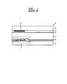
- FIG. 1is a view showing a cross-section of a general liquid crystal display device.
- the liquid crystal display device 1comprises a first substrate 5 , a second substrate 3 , and a liquid crystal layer 7 formed between the first substrate 5 and the second substrate 3 .
- the first substrate 5is a driving device array substrate, and a plurality of pixels are formed on the first substrate 5 and a driving device 9 such as a thin film transistor is formed on the respective pixel.
- the second substrate 3is a color filter substrate, and a color filter layer 2 for realizing actual colors and a black matrix 8 for blocking light leakage are formed thereon.
- a pixel electrode 6 and a common electrode 4are formed on the first substrate 5 and the second substrate 3 respectively, and an alignment layer (not shown) for orienting liquid crystal molecules of the liquid crystal layer 7 is applied thereon.
- the liquid crystal display device constructed as aboveis formed by a driving device array substrate process and a color filter substrate process respectively.
- the driving device array substrate processforms a plurality of gate lines and data line arranged on the lower substrate 5 for defining pixel areas, forms the thin film transistor 9 , that is, the driving device connected to the gate line and to the data line on respective pixel area, and after that, forms a pixel electrode connected to the thin film transistor 9 for driving the liquid crystal layer according to a signal application through the thin film transistor.
- the color filter processforms the black matrix on the upper substrate 3 , forms the color filter 2 on upper part of the black matrix 8 , and forms the common electrode 4 on the color filter 2 .
- the pigment dispersing methodforms the color filter by coating, exposing, developing and burning pigment composition dispersed on a photoresist. Fabrication of the color filter using the pigment dispersing method will be described with reference to FIGS. 2A to 2D .
- a transparent substrate 21is prepared, material for forming black matrix, such as chrome and organic material, is coated on the substrate 21 , and after that, a black matrix pattern 22 is formed using a photolithographic process that includes a photo mask.
- materials for forming red (R) color filter layer 23are coated on the substrate 21 and black matrix pattern 22 .
- a predetermined areais the exposed using a photo mask 28 and developed to form the R color filter layer 23 a as shown in FIG. 2C .
- the above processis repeated using different materials to form the green (G) and blue (B) color filters layers 23 b and 23 c , as shown in FIG. 2 d.
- the fabrication method used to form the color filters according to the related artnot only are expensive photo masks used, but in addition, the photolithographic processes, which include the color filter coating, exposure, and development, are repeatedly performed to create the color filter.
- the expense of the photo masks as well as the time and costs associated with multiple fabrication stepsincrease the overall fabrication costs in forming the layer containing the color filters.
- one embodiment of the present inventionprovides a fabrication method of providing a color filter for a display device which is able to reduce processing time and to reduce fabrication cost.
- a fabrication methodfor forming a color filter.
- the methodincludes providing a plurality of clichés in which grooves are formed, each groove having one of a color ink and opaque material (which may be a black resin), transferring the color inks in the clichés onto a substrate to form a color filter, and transferring the opaque material in a first cliché onto the color filter. Red ink, green ink, and blue ink may be selected as the color inks.
- the methodmay comprise supplying the color inks to the grooves.
- Supplying the color inks to the groovesmay comprise providing a supplying container with at least one of the color inks, imparting the at least one of the color inks to an ink supplying roller from the supplying container, contacting the clichés with the ink supplying roller, and rolling the ink supplying roller on the clichés to apply the at least one of the color inks to the clichés.
- the methodmay further comprise providing a plurality of ink supplying rollers, and imparting only one of the color inks to each ink supplying roller.
- the methodmay further comprise rolling each ink supplying roller on only one of the clichés.
- Transferring the color inksmay comprise transferring the color inks in the grooves of the clichés onto a surface of a printing roller (which itself may comprise rolling the printing roller on the clichés) and transferring the color inks on the printing roller to the substrate (which itself may comprise rolling the printing roller containing the color inks on the substrate).
- Transferring the color inksmay comprise may comprise transferring each of the color inks from the groove of each cliché onto a surface of a printing roller, each cliché containing only one of the color inks and transferring the color inks to the substrate, the printing roller containing only a single color ink each time the printing roller is rolled on the substrate.
- Transferring each of the color inks from the groove of each cliché onto a surface of a printing rollermay comprise rolling the printing roller on the clichés while transferring the color inks on the printing roller to the substrate may comprise rolling the printing roller containing the color inks on the substrate.
- the color filtermay be hardened after forming the color filter on the substrate. UV radiation and/or heat may be applied to the color filter to harden the color filter.
- Transferring the opaque materialmay comprise supplying the groove of the first cliché with the opaque material, transferring the opaque material to a surface of a printing roller (which may comprise rolling the printing roller on the first cliché), and transferring the opaque material to a boundary area between the color inks forming the color filter (which may comprise rolling the printing roller containing the opaque material on the substrate on which the color filter is formed). UV radiation and/or heat may be applied to the opaque material to harden the opaque material.
- the methodmay also comprise removing excess color inks and/or opaque material from the grooves in the clichés prior to transferring the color inks in the clichés onto the substrate.
- the methodmay further comprise removing the excess color inks and/or opaque material by moving a blade along the clichés such that the grooves are substantially filled by the color inks and/or opaque material, the filled grooves are substantially planar with the remainder of the clichés, and the color inks and/or opaque material on the surface of the clichés not in the grooves are removed.
- the methodmay further comprise transferring all of the color inks to the substrate on a single transfer apparatus, and may further comprise disposing all of the color inks on the single transfer apparatus at the same time (i.e. rather than repeatedly disposing one or more of the color inks to the transfer apparatus).
- the methodmay further comprise removing color ink present on a transfer apparatus that transfers the color inks in the clichés onto the substrate (which may be the printing roller) from the transfer apparatus prior to a new color ink being transferred to the transfer apparatus.
- the method of fabricating a color filter in a display devicecomprises providing a plurality of clichés in which grooves are formed, supplying the clichés with color inks, rolling a first printing roller on a first cliché to transfer a first color ink in a groove of the first cliché onto a surface of the first printing roller, rolling the first printing roller on which the first color ink is transferred on a second cliché to transfer a second color ink in a groove of the second cliché onto the surface of the first printing roller, rolling the first printing roller on which the first and second color inks are transferred on a third cliché to transfer a third color ink in a groove of the third cliché onto the surface of the first printing roller, rolling the first printing roller on which the first, second, and third color inks are transferred on a substrate to apply the first, second, and third color inks to the substrate and form a color filter, supplying a opaque material in a groove of a fourth cliché, rolling a second printing roller on the fourth cliché to transfer the opaque material in the groove of
- a method of fabricating a color filter in a display devicecomprises supplying grooves of a plurality of clichés with color inks, rolling the first printing roller on a first cliché to transfer a first color ink in a groove of the first cliché to a surface of the first printing roller, rolling the first printing roller containing the first color ink on a substrate to apply the first color ink to the substrate, rolling the first printing roller on a second cliché to transfer a second color ink in a groove of the second cliché to the surface of the first printing roller, rolling the first printing roller containing the second color ink on the substrate containing the first color ink to apply the second color ink to the substrate, rolling the first printing roller on a third cliché to transfer a third color ink in a groove of the third cliché to the surface of the first printing roller, rolling the first printing roller containing the third color ink on the substrate containing the first and second color inks to apply the third color ink to the substrate, supplying a groove of a fourth cliché with opaque material and rolling
- FIG. 1is a cross-sectional view showing a liquid crystal display (LCD) device of the related art.
- LCDliquid crystal display
- FIGS. 2A , 2 B, 2 C, and 2 Dare views illustrating a fabrication method of a color filter substrate in a liquid crystal display device according to the related art
- FIGS. 3A , 3 B, and 3 Care views showing a pattern forming method according to a gravure offset printing method
- FIG. 4is a view showing a gravure offset printing apparatus
- FIGS. 5A , 5 B, 5 C, and 5 Dare views illustrating a fabrication method of the color filter in an LCD device according to the present invention.
- FIG. 6illustrates a fabrication method of the color filter in an LCD device according to another embodiment of the present invention.
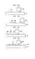
- FIGS. 3A , 3 B, and 3 Care views illustrating a pattern forming method according to a printing method, in particular, according to a gravure offset printing method.
- a groove 102is formed at one or more positions on a concave plate or cliché 100 corresponding to a pattern which will be formed on a substrate, and ink 104 is filled in the groove 102 .
- the filling of the ink 104 into the groove 102 of the cliché 100is performed by applying ink 104 to the cliché 100 and the removing a portion of the ink 104 by scraping off the excess/unwanted ink with a blade 108 that contacts the substrate 100 .
- excess ink 104 that is filled in the groove 102 and ink 104 remaining on the surface of the cliché 100 outside of the grooves 102is removed by moving the blade 108 along the cliché 100 , perhaps at a constant speed and in one direction for uniformity and ease of removal.
- An ink recycler or removal systemmay be provided to eliminate the excess ink removed from the cliché 100 and/or the excess ink that has built up on the blade 108 .
- the mechanical aspects associated with removal of the excess inkcan be set to any value desired so long as the excess ink is removed from the groove 102 and surface of the cliché 100 without damaging the cliché 100 and substantially all of the excess ink is removed.
- the ink 104 in the groove 102 of the cliché 100is transferred onto a surface of a printing roller 120 which is rotated as it contacts the surface of the cliché 100 (i.e. as the printing roller 120 or transfer apparatus rolls on the surface of the cliché 100 ).
- the printing roller 120may have substantially the same width as that of the substrate to be fabricated and has substantially the same circumference as the length of the cliché 100 . This permits the ink 104 filled in the groove 102 of the cliché 100 to be transferred onto the surface of the printing roller 120 with a single revolution of the printing roller 120 .
- the ink 104 transferred to the printing roller 120is applied to the substrate 121 .
- the printing roller 120rolls along the surface of the substrate 121 .
- the printing roller 120again may have substantially the same circumference as the length of the substrate 121 , which permits the ink on the printing roller 120 to be transferred to the substrate 121 with a single revolution of the printing roller 120 .
- ultraviolet radiation (UV) or heatis used to harden the ink 104 , thereby forming an ink pattern 125 .
- UVultraviolet radiation
- a color filtercan be formed on entire substrate 121 in a single rotation of the printing roller 120 .
- the desired patterncan be formed without using photolithographic processes, and therefore, the photo mask process of the related art including mask creation, application of photoresist, mask alignment, and exposure and development of the photoresist, can be omitted, reducing the fabrication time and cost.
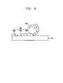
- FIG. 4 and FIGS. 5A to 5Dare views illustrating a fabrication method of the color filter for the display device according to the present invention.
- FIG. 4shows a printing apparatus for fabricating the color filter of the present invention.
- FIGS. 5A to 5Dare views illustrating the fabrication method of the color filter using the above printing apparatus. Although this method may be employed during fabrication LCDs, it also may be used for other types of displays that use color filters and that are amenable to a similar type of roller process.
- the printing apparatuscontains a plurality of clichés 200 ( 200 a , 200 b , 200 c , 200 d ) for forming red (R), green (G), and blue (B) color filters and a black matrix pattern.
- Each of the clichés 200is similar to the cliché 100 of FIGS. 3A to 3C , without the individual features being shown in FIG. 4 .
- the printing apparatusalso includes a plurality of printing rollers 220 ( 220 a and 220 b ) that are used to transfer the red, green, blue color inks and black resin (or opaque material that is opaque to radiation to be applied to the substrate) filled in the cliché 200 onto the substrate 221 as well as a plurality of ink supplying rollers 230 ( 230 a , 230 b , 230 c , 230 d ) that supply the red, green, and blue color inks and the black resin to the clichés 200 .
- An ink container 240provides the ink supplying roller 230 with the particular ink to be applied to one of the clichés 200 .
- the printing apparatusalso includes a blade (not shown) for removing the ink that remains on the surface of each cliché 200 after the ink has been supplied to the cliché 200 as described above.
- a particular color inkis filled in the ink supplying container 240 .
- the ink supplying roller 230is then moved to be in contact with the ink supplying container 240 and rotated to coat the color ink over at least a portion of the surface of the ink supplying roller 230 that is to contact the cliché 200 associated with that color.
- the ink supplying roller 230is moved away from the ink supplying container 240 to contact the associated cliché 200 and rotated to apply the color ink to that cliché 200 .
- the ink on the surface of the cliché 200is subsequently moved using the blade (not shown) such that the groove of the cliché 200 is filled with the ink and planarized while excess ink remaining on the surface of the cliché 200 is removed.
- the bladenot shown
- the ink supplying containermay then be cleaned and refilled with a different color ink and the process repeated using a different ink supplying roller and cliché until the desired number of clichés are filled.
- the ink supplying containermay have different compartments filled with different color inks, the different ink supplying rollers being moved and supplied with ink one after the other, and then the clichés filled one after the other by the different ink supplying rollers.
- the different ink supplying rollersare moved such that only the ink supplying roller associated with a particular color contacts (and is supplied with) that particular color ink and contacts (and transfers) that particular color ink only to the associated cliché.
- only a single ink supplying rollermay be used, which may be cleaned after each transferal of ink to the respective cliché.
- a single clichémay be used.
- that clichécontains grooves that are adjacent to each other and each groove is filled with a color that is different from the color in the adjacent groove such that the printing roller will pick up the ink from the cliché and transfer the ink to the substrate to form the color filter.
- the groovesmay be filled with ink colors red, green, and blue, in that order, one or multiple times as desired.
- the ink supplying container 240supplies red color ink to the first ink supplying roller 230 a , which then contacts and rotates on the first cliché 200 a to apply the red ink to the surface of the first cliché 200 a .
- the green color ink and the blue color inkare supplied to the second ink supplying roller 230 b and third ink supplying roller 230 c , and which apply the green ink and the blue ink to the surfaces of the second and third cliché 200 b and 200 c , respectively.
- the red, green and blue color inksare filled in the grooves of the clichés 200 by the ink supplying rollers 230 .
- the first printing roller 220 acontacts and rotates on (i.e. rolls along) the surface of the first cliché 200 a to transfer the red ink onto the surface of the first printing roller 220 a , and the red ink transferred to the first printing roller 220 a is then applied to the substrate 221 to form the red color filter 223 a , as shown in FIG. 5A .
- the first printing roller 220 acontacts and rotates on the surface of the second cliché 220 b , thereby transferring the green color ink onto the surface of the first printing roller 220 a .
- the green color ink transferred to the first printing roller 220 ais subsequently applied to the substrate 221 on which the red color filter 223 a is formed to form the green color filter 223 b .
- the blue color inkis printed on the substrate 221 on which the red and green color filters 223 a and 223 b are formed by repeating the above process to form the blue color filter 223 c .
- the color filter 223is hardened by applying UV radiation or heat to the substrate 221 prior to the black resin being formed on the color filter 223 to enable the color filter 223 to withstand the stress of the transfer process.
- the black resinis supplied to the fourth ink supplying roller 230 d , which then contacts and rotates on the fourth cliché 200 d , thereby filling the groove of the fourth cliché 200 d with the black resin.
- the black resinmay be supplied to the fourth cliché 200 d at the same time that the color inks are supplied to the other clichés, or may be supplied after the color inks are transferred to the substrate 221 .
- the second printing roller 220 brolls along the surface of the fourth cliché 200 d to transfer the black resin in the groove to the surface of the second printing roller 220 b . After that, as shown in FIG.
- the black resin transferred to the surface of the second printing roller 220 bis transferred to the color filter 223 when the second printing roller 220 b rolls along the color filter 223 , thereby printing the black resin on a boundary region of the red, green and blue color filter 223 .
- UV radiation or heatis provided to the black resin to form the black matrix 225 .
- the first printing roller 220 acontacts and rotates on the first, second, and third clichés 200 a , 200 b , and 200 c in which the red, green and blue color inks are filled such that the red, green and blue color inks are transferred onto the first printing roller 220 a in a contiguous manner.
- the inksare transferred onto the printing roller 220 a such that the color inks are all disposed on the printing roller 220 a at the same time, rather than only one color at a time being disposed on the printing roller 220 a (i.e., all of the color inks are transferred on a single transfer apparatus at the same time).
- the color inksare then applied to the substrate 221 to form the red, green and blue color filters 223 a , 223 b , and 223 c one after the other so that the overall color filter 223 is formed by the first printing roller 220 a in one pass of the substrate 221 (either in a single rotation or multiple revolutions).
- the fabrication time in producing the color filtercan be further reduced.
- the characteristics associated with the transferal of the ink to the cliché by the ink supply roller and to the substrate by the printing roller, the type of roller or pressure between the roller and cliché or substratecan be set to any value desired so long as the ink is transferred without damaging the cliché or substrate.
- the clichémay be formed from a metal or ceramic that is hard enough to withstand the cleaning and transferal processes described above, as well as being relatively easy to clean.
- surface of the rollermay be formed from a material that permits the ink or resin to readily adhere to the surface of the roller when the ink or resin is transferred to the roller and permits the ink or resin to be readily removed from the surface of the roller when the ink or resin is transferred to the substrate.
- the roller materialis also formed from a material that is relatively easy to clean while being resilient enough to withstand the cleaning process.
- the present inventionprovides a method of fabrication for a color filter of a display device.
- the color filter layeris applied, and a photolithographic process repeated to form the red, green and blue color filter pattern.
- the color filter and the black matrixare formed using a printing method. This eliminates the photolithographic process, thereby reducing fabrication time and cost.
- the entire color filter layeris printed at the same time, which further reduces the fabrication time and cost.
- the color filter and the black matrixcan be formed using screen printing, ink jet printing or flexography. That is, one advantage of the present invention is to form the color filter substrate without using a photolithographic process, and other embodiments or modified embodiments using the above concepts should be included in the scope of the present invention.
Landscapes
- Physics & Mathematics (AREA)
- General Health & Medical Sciences (AREA)
- Toxicology (AREA)
- Health & Medical Sciences (AREA)
- Optics & Photonics (AREA)
- General Physics & Mathematics (AREA)
- Thermal Sciences (AREA)
- Manufacturing & Machinery (AREA)
- Engineering & Computer Science (AREA)
- Nonlinear Science (AREA)
- Electromagnetism (AREA)
- Mathematical Physics (AREA)
- Chemical & Material Sciences (AREA)
- Crystallography & Structural Chemistry (AREA)
- Optical Filters (AREA)
- Liquid Crystal (AREA)
- Printing Methods (AREA)
Abstract
Description
Claims (28)
Applications Claiming Priority (2)
| Application Number | Priority Date | Filing Date | Title |
|---|---|---|---|
| KR1020020085631AKR100945356B1 (en) | 2002-12-27 | 2002-12-27 | Method for manufacturing color filter of liquid crystal display device |
| KRP2002-85631 | 2002-12-27 |
Publications (2)
| Publication Number | Publication Date |
|---|---|
| US20040123753A1 US20040123753A1 (en) | 2004-07-01 |
| US7243599B2true US7243599B2 (en) | 2007-07-17 |
Family
ID=32653182
Family Applications (1)
| Application Number | Title | Priority Date | Filing Date |
|---|---|---|---|
| US10/679,060Expired - LifetimeUS7243599B2 (en) | 2002-12-27 | 2003-10-03 | Method of fabricating color filter in display device |
Country Status (2)
| Country | Link |
|---|---|
| US (1) | US7243599B2 (en) |
| KR (1) | KR100945356B1 (en) |
Cited By (5)
| Publication number | Priority date | Publication date | Assignee | Title |
|---|---|---|---|---|
| US20050241513A1 (en)* | 2004-04-30 | 2005-11-03 | Hong-Suk Yoo | Method for forming black matrix of liquid crystal display device |
| US20060021529A1 (en)* | 2004-07-29 | 2006-02-02 | Fujitsu Limited | Molding material transfer method and substrate structure |
| US20060162594A1 (en)* | 2005-01-26 | 2006-07-27 | Yoshinori Nakaya | Single color press and method of operating same, and method of manufacturing liquid crystal color filter |
| US20090128771A1 (en)* | 2007-08-16 | 2009-05-21 | Industrial Technology Research Institute | Fabrication methods for liquid crystal display devices |
| US20110187982A1 (en)* | 2007-04-14 | 2011-08-04 | Inudstrial Technology Research Institute | Color cholesteric liquid crystal display devices and fabrication methods thereof |
Families Citing this family (21)
| Publication number | Priority date | Publication date | Assignee | Title |
|---|---|---|---|---|
| US20060199086A1 (en)* | 2005-03-04 | 2006-09-07 | Burkum Philip S | System and method for creating a color filter for a display panel |
| US7582331B2 (en)* | 2005-06-30 | 2009-09-01 | Lg. Display Co., Ltd. | Printing apparatus and fabricating method thereof |
| KR101192788B1 (en)* | 2005-10-13 | 2012-10-18 | 엘지디스플레이 주식회사 | Printing Device System and Patterning method using the same |
| KR101157967B1 (en)* | 2005-11-28 | 2012-06-25 | 엘지디스플레이 주식회사 | Printing system and Method of manufacturing of Liquid Crystal Display Device using the same |
| KR101255295B1 (en)* | 2005-11-28 | 2013-04-15 | 엘지디스플레이 주식회사 | Printing Device System and Patterning method using the same |
| KR101319273B1 (en)* | 2005-12-29 | 2013-10-16 | 엘지디스플레이 주식회사 | Printing plate stage, Printing system and Method of manufacturing of Liquid Crystal Display Device using the same |
| KR101255294B1 (en)* | 2005-12-29 | 2013-04-23 | 엘지디스플레이 주식회사 | Printing Apparatus and Method of manufacturing Liquid Crystal Display Device using the same |
| KR101192748B1 (en)* | 2005-12-30 | 2012-10-18 | 엘지디스플레이 주식회사 | Printing Apparatus and Method of manufacturing Liquid Crystal Display Device using the same |
| KR101264687B1 (en)* | 2006-06-21 | 2013-05-16 | 엘지디스플레이 주식회사 | Printing Apparatus, Patterning Method and Method of Manufacturing Liquid Crystal Display Device the Same |
| KR101287385B1 (en)* | 2007-01-31 | 2013-07-18 | 엘지디스플레이 주식회사 | Resist printing pattern device and method of forming cliche |
| KR101258354B1 (en)* | 2009-04-01 | 2013-04-30 | 가부시키가이샤 슈호 | Printing method and object to be printed |
| KR101419573B1 (en)* | 2010-11-22 | 2014-07-15 | 한국전자통신연구원 | offset printer and printing method of the same |
| JP2013004649A (en)* | 2011-06-15 | 2013-01-07 | Sony Corp | Film manufacturing method and manufacturing method of display device |
| CN102566134A (en)* | 2011-12-02 | 2012-07-11 | 深圳市华星光电技术有限公司 | Method for manufacturing substrate with colored film and manufacturing device |
| US20140098332A1 (en)* | 2012-10-10 | 2014-04-10 | Apple Inc. | Displays With Logos and Alignment Marks |
| WO2014115367A1 (en)* | 2013-01-25 | 2014-07-31 | 凸版印刷株式会社 | Color filter substrate, liquid-crystal display device, and method for manufacturing color filter substrate |
| JP6685675B2 (en)* | 2015-09-07 | 2020-04-22 | 株式会社Joled | Organic EL device, organic EL display panel using the same, and method for manufacturing organic EL display panel |
| WO2017188767A1 (en)* | 2016-04-27 | 2017-11-02 | 이하영 | Multi-color gravure offset printing device and printing method |
| JP2018132511A (en)* | 2017-02-17 | 2018-08-23 | 株式会社リコー | Thickness detection device, image forming device |
| TWI661947B (en)* | 2017-11-17 | 2019-06-11 | 財團法人工業技術研究院 | Gravure offset printing apparatus |
| KR20230026587A (en)* | 2021-08-17 | 2023-02-27 | 삼성디스플레이 주식회사 | Method of manufcaturing a display device |
Citations (26)
| Publication number | Priority date | Publication date | Assignee | Title |
|---|---|---|---|---|
| US4294650A (en) | 1977-02-18 | 1981-10-13 | Firma Standex International Gmbh | Method of and apparatus for producing embossing tools |
| JPS63205608A (en) | 1987-02-23 | 1988-08-25 | Matsushita Electric Ind Co Ltd | Manufacturing method of color filter for liquid crystal display |
| US4841857A (en)* | 1986-03-03 | 1989-06-27 | Nissha Printing Co., Ltd. | Thin-film forming apparatus |
| US5017223A (en)* | 1988-07-29 | 1991-05-21 | Canon Kabushiki Kaisha | Recording material |
| JPH03280416A (en) | 1990-03-29 | 1991-12-11 | G T C:Kk | Resist pattern forming method |
| EP0471628A1 (en) | 1990-08-09 | 1992-02-19 | Gtc Corporation | Thin film transistor circuit and its manufacturing |
| JPH04239684A (en) | 1991-01-24 | 1992-08-27 | G T C:Kk | Method for forming of fine pattern |
| JPH04249189A (en) | 1991-02-01 | 1992-09-04 | G T C:Kk | Method for forming fine regist pattern |
| JPH04296724A (en) | 1991-03-26 | 1992-10-21 | G T C:Kk | Printing method for fine pattern |
| JPH0511270A (en) | 1991-07-03 | 1993-01-19 | Toshiba Corp | Mask pattern formation method |
| US5259926A (en) | 1991-09-24 | 1993-11-09 | Hitachi, Ltd. | Method of manufacturing a thin-film pattern on a substrate |
| JPH06202314A (en) | 1993-01-05 | 1994-07-22 | G T C:Kk | Printing plate, method of manufacturing the same, and method of forming pattern using the printing plate |
| US5335595A (en)* | 1992-07-01 | 1994-08-09 | Nsk Ltd. | Roller offset printing apparatus |
| US5366760A (en)* | 1990-04-12 | 1994-11-22 | Matsushita Electric Industrial Co., Ltd. | Conductive ink composition and method of forming a conductive thick film pattern |
| JPH07240523A (en) | 1994-02-25 | 1995-09-12 | G T C:Kk | Method of forming thin film transistor circuit by offset printing method |
| US5514503A (en) | 1994-10-17 | 1996-05-07 | Corning Incorporated | Apparatus and method for printing a color filter |
| US5544582A (en) | 1993-11-03 | 1996-08-13 | Corning Incorporated | Method for printing a color filter |
| US5678483A (en) | 1994-02-16 | 1997-10-21 | Corning Incorporated | Method for printing a black border for a color filter |
| US5701815A (en) | 1993-11-03 | 1997-12-30 | Corning Incorporated | Method of printing a color filter |
| US5824374A (en)* | 1996-07-22 | 1998-10-20 | Optical Coating Laboratory, Inc. | In-situ laser patterning of thin film layers during sequential depositing |
| US5925484A (en)* | 1996-08-02 | 1999-07-20 | Toppan Printing Co., Ltd. | Black photosensitive resin composition, color filter made by using the same, and a process for the production thereof |
| US6001515A (en) | 1993-11-03 | 1999-12-14 | Corning Incorporated | Method for printing a color filter |
| JP2001183647A (en)* | 1999-12-22 | 2001-07-06 | Matsushita Electric Ind Co Ltd | Method for forming color filter of liquid crystal display panel |
| US6356318B1 (en) | 1999-06-28 | 2002-03-12 | Alps Electric Co., Ltd. | Active-matrix liquid crystal display having storage capacitors of area smaller than that of pixel electrodes |
| US6488376B1 (en)* | 1999-10-28 | 2002-12-03 | Ocular Sciences, Inc. | Tinted contact lens and method for making same |
| US20030063238A1 (en)* | 2001-09-28 | 2003-04-03 | Lg. Philips Lcd Co., Ltd. | Method of fabricating color filter panel for liquid crystal display device using thermal imaging |
Family Cites Families (2)
| Publication number | Priority date | Publication date | Assignee | Title |
|---|---|---|---|---|
| JPH0743514A (en)* | 1993-08-02 | 1995-02-14 | Fujitsu Ltd | Color filter manufacturing method |
| KR100638410B1 (en)* | 1997-07-31 | 2007-07-12 | 코닝 인코포레이티드 | Method of Making an Imaged Ink Pattern |
- 2002
- 2002-12-27KRKR1020020085631Apatent/KR100945356B1/ennot_activeExpired - Lifetime
- 2003
- 2003-10-03USUS10/679,060patent/US7243599B2/ennot_activeExpired - Lifetime
Patent Citations (27)
| Publication number | Priority date | Publication date | Assignee | Title |
|---|---|---|---|---|
| US4294650A (en) | 1977-02-18 | 1981-10-13 | Firma Standex International Gmbh | Method of and apparatus for producing embossing tools |
| US4841857A (en)* | 1986-03-03 | 1989-06-27 | Nissha Printing Co., Ltd. | Thin-film forming apparatus |
| JPS63205608A (en) | 1987-02-23 | 1988-08-25 | Matsushita Electric Ind Co Ltd | Manufacturing method of color filter for liquid crystal display |
| US5017223A (en)* | 1988-07-29 | 1991-05-21 | Canon Kabushiki Kaisha | Recording material |
| JPH03280416A (en) | 1990-03-29 | 1991-12-11 | G T C:Kk | Resist pattern forming method |
| US5366760A (en)* | 1990-04-12 | 1994-11-22 | Matsushita Electric Industrial Co., Ltd. | Conductive ink composition and method of forming a conductive thick film pattern |
| JPH0494115A (en) | 1990-08-09 | 1992-03-26 | G T C:Kk | Method for manufacturing thin film transistor circuits |
| EP0471628A1 (en) | 1990-08-09 | 1992-02-19 | Gtc Corporation | Thin film transistor circuit and its manufacturing |
| JPH04239684A (en) | 1991-01-24 | 1992-08-27 | G T C:Kk | Method for forming of fine pattern |
| JPH04249189A (en) | 1991-02-01 | 1992-09-04 | G T C:Kk | Method for forming fine regist pattern |
| JPH04296724A (en) | 1991-03-26 | 1992-10-21 | G T C:Kk | Printing method for fine pattern |
| JPH0511270A (en) | 1991-07-03 | 1993-01-19 | Toshiba Corp | Mask pattern formation method |
| US5259926A (en) | 1991-09-24 | 1993-11-09 | Hitachi, Ltd. | Method of manufacturing a thin-film pattern on a substrate |
| US5335595A (en)* | 1992-07-01 | 1994-08-09 | Nsk Ltd. | Roller offset printing apparatus |
| JPH06202314A (en) | 1993-01-05 | 1994-07-22 | G T C:Kk | Printing plate, method of manufacturing the same, and method of forming pattern using the printing plate |
| US5544582A (en) | 1993-11-03 | 1996-08-13 | Corning Incorporated | Method for printing a color filter |
| US5701815A (en) | 1993-11-03 | 1997-12-30 | Corning Incorporated | Method of printing a color filter |
| US6001515A (en) | 1993-11-03 | 1999-12-14 | Corning Incorporated | Method for printing a color filter |
| US5678483A (en) | 1994-02-16 | 1997-10-21 | Corning Incorporated | Method for printing a black border for a color filter |
| JPH07240523A (en) | 1994-02-25 | 1995-09-12 | G T C:Kk | Method of forming thin film transistor circuit by offset printing method |
| US5514503A (en) | 1994-10-17 | 1996-05-07 | Corning Incorporated | Apparatus and method for printing a color filter |
| US5824374A (en)* | 1996-07-22 | 1998-10-20 | Optical Coating Laboratory, Inc. | In-situ laser patterning of thin film layers during sequential depositing |
| US5925484A (en)* | 1996-08-02 | 1999-07-20 | Toppan Printing Co., Ltd. | Black photosensitive resin composition, color filter made by using the same, and a process for the production thereof |
| US6356318B1 (en) | 1999-06-28 | 2002-03-12 | Alps Electric Co., Ltd. | Active-matrix liquid crystal display having storage capacitors of area smaller than that of pixel electrodes |
| US6488376B1 (en)* | 1999-10-28 | 2002-12-03 | Ocular Sciences, Inc. | Tinted contact lens and method for making same |
| JP2001183647A (en)* | 1999-12-22 | 2001-07-06 | Matsushita Electric Ind Co Ltd | Method for forming color filter of liquid crystal display panel |
| US20030063238A1 (en)* | 2001-09-28 | 2003-04-03 | Lg. Philips Lcd Co., Ltd. | Method of fabricating color filter panel for liquid crystal display device using thermal imaging |
Cited By (9)
| Publication number | Priority date | Publication date | Assignee | Title |
|---|---|---|---|---|
| US20050241513A1 (en)* | 2004-04-30 | 2005-11-03 | Hong-Suk Yoo | Method for forming black matrix of liquid crystal display device |
| US7406915B2 (en)* | 2004-04-30 | 2008-08-05 | Lg Display Co., Ltd. | Method for forming black matrix of liquid crystal display device |
| US20060021529A1 (en)* | 2004-07-29 | 2006-02-02 | Fujitsu Limited | Molding material transfer method and substrate structure |
| US7530305B2 (en)* | 2004-07-29 | 2009-05-12 | Hitachi Limited | Molding material transfer method and substrate structure |
| US20060162594A1 (en)* | 2005-01-26 | 2006-07-27 | Yoshinori Nakaya | Single color press and method of operating same, and method of manufacturing liquid crystal color filter |
| US7516697B2 (en)* | 2005-01-26 | 2009-04-14 | Mitsubishi Heavy Industries, Ltd | Single color press and method of operating same, and method of manufacturing liquid crystal color filter |
| US20110187982A1 (en)* | 2007-04-14 | 2011-08-04 | Inudstrial Technology Research Institute | Color cholesteric liquid crystal display devices and fabrication methods thereof |
| US8502952B2 (en) | 2007-04-14 | 2013-08-06 | Industrial Technology Research Institute | Color cholesteric liquid crystal display devices and fabrication methods thereof |
| US20090128771A1 (en)* | 2007-08-16 | 2009-05-21 | Industrial Technology Research Institute | Fabrication methods for liquid crystal display devices |
Also Published As
| Publication number | Publication date |
|---|---|
| US20040123753A1 (en) | 2004-07-01 |
| KR20040059097A (en) | 2004-07-05 |
| KR100945356B1 (en) | 2010-03-09 |
Similar Documents
| Publication | Publication Date | Title |
|---|---|---|
| US7243599B2 (en) | Method of fabricating color filter in display device | |
| US20100290143A1 (en) | Color filter and apparatus and method of manufacturing the same | |
| US8186271B2 (en) | Method for manufacturing printing plate | |
| JP2004212978A (en) | Alignment film formation method | |
| US20050092712A1 (en) | Printing system and method for fabricating a liquid crystal display device | |
| US20100157211A1 (en) | Liquid crystal display device and method for manufacturing the same | |
| JP3902335B2 (en) | Photosensitive resin plate and manufacturing method thereof | |
| KR101291878B1 (en) | Roller apparatus, printing method and method of fabricating liquid crystal display device using the same | |
| JP4140771B2 (en) | Pattern forming method for liquid crystal display element | |
| US7390422B2 (en) | Method for manufacturing printing plate | |
| US7520220B2 (en) | Cliché unit, printing apparatus, and printing method using the same | |
| CN101100145A (en) | Printing device system, patterning method using same, and method of manufacturing liquid crystal display device using same | |
| CN1716033A (en) | Apparatus and method for manufacturing color filters for liquid crystal display devices | |
| US7169517B2 (en) | Method of fabricating a color filter in liquid crystal display device without using a photo mask | |
| KR101250236B1 (en) | Color filter substrate and manufacturing method of liquid crystal display device comprising the same | |
| US7406915B2 (en) | Method for forming black matrix of liquid crystal display device | |
| JP2012027469A (en) | Device and method for repairing liquid crystal display panel | |
| CN1971416B (en) | Printing plate, method of manufacturing of printing plate and liquid crystal display device using the same | |
| US8105762B2 (en) | Method for forming pattern using printing process | |
| KR100990312B1 (en) | Spacer Formation Method of Liquid Crystal Display Device | |
| KR100839455B1 (en) | printer | |
| KR100972486B1 (en) | Manufacturing method of liquid crystal display device | |
| KR20070041041A (en) | Engraved blanket structure for offset printing | |
| KR20060116109A (en) | Apparatus and method for forming color filter and liquid crystal display comprising color filter formed thereby | |
| KR20060132137A (en) | Manufacturing Method of Printing Plate |
Legal Events
| Date | Code | Title | Description |
|---|---|---|---|
| AS | Assignment | Owner name:LG. PHILIPS LCD CO., LTD., KOREA, REPUBLIC OF Free format text:ASSIGNMENT OF ASSIGNORS INTEREST;ASSIGNORS:YOO, HONG-SUK;BAEK, MYOUNG-KEE;REEL/FRAME:014584/0433 Effective date:20030924 | |
| STCF | Information on status: patent grant | Free format text:PATENTED CASE | |
| FEPP | Fee payment procedure | Free format text:PAYOR NUMBER ASSIGNED (ORIGINAL EVENT CODE: ASPN); ENTITY STATUS OF PATENT OWNER: LARGE ENTITY | |
| AS | Assignment | Owner name:LG DISPLAY CO., LTD., KOREA, REPUBLIC OF Free format text:CHANGE OF NAME;ASSIGNOR:LG. PHILIPS CO., LTD.;REEL/FRAME:020963/0710 Effective date:20080229 Owner name:LG DISPLAY CO., LTD.,KOREA, REPUBLIC OF Free format text:CHANGE OF NAME;ASSIGNOR:LG. PHILIPS CO., LTD.;REEL/FRAME:020963/0710 Effective date:20080229 | |
| FEPP | Fee payment procedure | Free format text:PAYER NUMBER DE-ASSIGNED (ORIGINAL EVENT CODE: RMPN); ENTITY STATUS OF PATENT OWNER: LARGE ENTITY Free format text:PAYOR NUMBER ASSIGNED (ORIGINAL EVENT CODE: ASPN); ENTITY STATUS OF PATENT OWNER: LARGE ENTITY | |
| FPAY | Fee payment | Year of fee payment:4 | |
| FPAY | Fee payment | Year of fee payment:8 | |
| MAFP | Maintenance fee payment | Free format text:PAYMENT OF MAINTENANCE FEE, 12TH YEAR, LARGE ENTITY (ORIGINAL EVENT CODE: M1553); ENTITY STATUS OF PATENT OWNER: LARGE ENTITY Year of fee payment:12 |